WO2021153061A1 - 検査用ソケット - Google Patents
検査用ソケット Download PDFInfo
- Publication number
- WO2021153061A1 WO2021153061A1 PCT/JP2020/046951 JP2020046951W WO2021153061A1 WO 2021153061 A1 WO2021153061 A1 WO 2021153061A1 JP 2020046951 W JP2020046951 W JP 2020046951W WO 2021153061 A1 WO2021153061 A1 WO 2021153061A1
- Authority
- WO
- WIPO (PCT)
- Prior art keywords
- package
- inspected
- pressing
- contact probe
- axis
- Prior art date
Links
Images


Classifications
-
- G—PHYSICS
- G01—MEASURING; TESTING
- G01R—MEASURING ELECTRIC VARIABLES; MEASURING MAGNETIC VARIABLES
- G01R1/00—Details of instruments or arrangements of the types included in groups G01R5/00 - G01R13/00 and G01R31/00
- G01R1/02—General constructional details
- G01R1/06—Measuring leads; Measuring probes
- G01R1/067—Measuring probes
- G01R1/06711—Probe needles; Cantilever beams; "Bump" contacts; Replaceable probe pins
- G01R1/06716—Elastic
- G01R1/06722—Spring-loaded
-
- G—PHYSICS
- G01—MEASURING; TESTING
- G01R—MEASURING ELECTRIC VARIABLES; MEASURING MAGNETIC VARIABLES
- G01R1/00—Details of instruments or arrangements of the types included in groups G01R5/00 - G01R13/00 and G01R31/00
- G01R1/02—General constructional details
- G01R1/04—Housings; Supporting members; Arrangements of terminals
- G01R1/0408—Test fixtures or contact fields; Connectors or connecting adaptors; Test clips; Test sockets
- G01R1/0433—Sockets for IC's or transistors
- G01R1/0483—Sockets for un-leaded IC's having matrix type contact fields, e.g. BGA or PGA devices; Sockets for unpackaged, naked chips
-
- G—PHYSICS
- G01—MEASURING; TESTING
- G01R—MEASURING ELECTRIC VARIABLES; MEASURING MAGNETIC VARIABLES
- G01R1/00—Details of instruments or arrangements of the types included in groups G01R5/00 - G01R13/00 and G01R31/00
- G01R1/02—General constructional details
- G01R1/04—Housings; Supporting members; Arrangements of terminals
- G01R1/0408—Test fixtures or contact fields; Connectors or connecting adaptors; Test clips; Test sockets
- G01R1/0433—Sockets for IC's or transistors
- G01R1/0441—Details
- G01R1/0466—Details concerning contact pieces or mechanical details, e.g. hinges or cams; Shielding
-
- G—PHYSICS
- G01—MEASURING; TESTING
- G01R—MEASURING ELECTRIC VARIABLES; MEASURING MAGNETIC VARIABLES
- G01R1/00—Details of instruments or arrangements of the types included in groups G01R5/00 - G01R13/00 and G01R31/00
- G01R1/02—General constructional details
- G01R1/06—Measuring leads; Measuring probes
- G01R1/067—Measuring probes
- G01R1/073—Multiple probes
- G01R1/07307—Multiple probes with individual probe elements, e.g. needles, cantilever beams or bump contacts, fixed in relation to each other, e.g. bed of nails fixture or probe card
- G01R1/07342—Multiple probes with individual probe elements, e.g. needles, cantilever beams or bump contacts, fixed in relation to each other, e.g. bed of nails fixture or probe card the body of the probe being at an angle other than perpendicular to test object, e.g. probe card
-
- G—PHYSICS
- G01—MEASURING; TESTING
- G01R—MEASURING ELECTRIC VARIABLES; MEASURING MAGNETIC VARIABLES
- G01R1/00—Details of instruments or arrangements of the types included in groups G01R5/00 - G01R13/00 and G01R31/00
- G01R1/02—General constructional details
- G01R1/06—Measuring leads; Measuring probes
- G01R1/067—Measuring probes
- G01R1/073—Multiple probes
- G01R1/07307—Multiple probes with individual probe elements, e.g. needles, cantilever beams or bump contacts, fixed in relation to each other, e.g. bed of nails fixture or probe card
- G01R1/07364—Multiple probes with individual probe elements, e.g. needles, cantilever beams or bump contacts, fixed in relation to each other, e.g. bed of nails fixture or probe card with provisions for altering position, number or connection of probe tips; Adapting to differences in pitch
-
- H—ELECTRICITY
- H01—ELECTRIC ELEMENTS
- H01L—SEMICONDUCTOR DEVICES NOT COVERED BY CLASS H10
- H01L23/00—Details of semiconductor or other solid state devices
- H01L23/32—Holders for supporting the complete device in operation, i.e. detachable fixtures
-
- H—ELECTRICITY
- H01—ELECTRIC ELEMENTS
- H01R—ELECTRICALLY-CONDUCTIVE CONNECTIONS; STRUCTURAL ASSOCIATIONS OF A PLURALITY OF MUTUALLY-INSULATED ELECTRICAL CONNECTING ELEMENTS; COUPLING DEVICES; CURRENT COLLECTORS
- H01R33/00—Coupling devices specially adapted for supporting apparatus and having one part acting as a holder providing support and electrical connection via a counterpart which is structurally associated with the apparatus, e.g. lamp holders; Separate parts thereof
- H01R33/74—Devices having four or more poles, e.g. holders for compact fluorescent lamps
- H01R33/76—Holders with sockets, clips, or analogous contacts adapted for axially-sliding engagement with parallely-arranged pins, blades, or analogous contacts on counterpart, e.g. electronic tube socket
Definitions
- the present invention relates to an inspection socket.
- the inspection socket is for electrically connecting the inspection target IC package to the inspection device, and includes a plurality of contact probes arranged so as to correspond to the arrangement of the electrode terminals of the inspection target IC package.
- Patent Document 1 a socket in which the contact probe is tilted so as to make oblique contact with the electrode terminal is also known (see Patent Document 1).
- Patent Document 1 the inclination directions of the contact probes are reversed with respect to the center of the arrangement so that the arrangements of the plurality of contact probes are symmetrical. This is because when the contact probe is brought into contact with the electrode terminals, the IC package to be inspected does not move in the direction parallel to the arrangement of the electrode terminals, and the terminal surface is scratched to ensure the scrubbing operation.
- the tip of the contact probe can be surely brought into contact with the electrode terminal under the oxide film, and the continuity between the two can be ensured.
- Patent Document 1 it is necessary to incline the support holes (stepped holes) of the contact probes in different directions in the support portion that supports each contact probe. This leads to an increase in the size of the inspection socket and complicated processing of the support portion, resulting in an increase in cost. Further, depending on the arrangement and number of electrode terminals in the IC package to be inspected, it may be difficult to arrange the contact probes symmetrically.
- An example of an object of the present invention is to allow a stable scrubbing operation when the contact probe and the electrode terminal of the IC package to be inspected come into contact with each other.
- An aspect of the present invention is an inspection in which a pin block that exposes the tip of a contact probe from an exposed surface and supports the contact probe by inclining it in a predetermined direction with respect to a direction perpendicular to the exposed surface, and contacting the contact probe.
- An inspection socket including a pressing portion for pushing the target IC package.
- the pin block can support the contact probe by inclining it in a predetermined direction.
- the IC package to be inspected can be pushed by the pressing portion. Since the pin block is tilted in a predetermined direction, when the contact probe comes into contact with the electrode terminal of the IC package to be inspected, the IC package to be inspected moves based on the tilt direction of the contact probe, and scrubbing operation is unlikely to occur. May occur. However, since the IC package to be inspected is pushed by the pressing portion, such a situation can be suppressed, and a stable scrub operation can be performed when the contact probe and the electrode terminal of the IC package to be inspected come into contact with each other.
- each contact probe since the inclination direction of each contact probe may be the same, it is not necessary to increase the size of the pin block, and complicated processing is not required for the pin block that supports the contact probe. Further, since the IC package to be inspected is pushed by the pressing portion, the positioning accuracy of the IC package to be inspected can be improved as compared with the case where there is no pressing portion.
- FIG. 2 is a sectional view taken along line III-III in FIG.
- the top view which shows the structural example of the socket body in the modification 1.
- FIG. The top view which shows the structural example of the socket body in the modification 2.
- Another diagram for explaining the position change of the taper member and the spring in the modification 4. The schematic diagram which shows the relationship between the inclination direction of a contact probe and the direction which pushes an IC package to be inspected.
- the vertical direction of the inspection socket 1 is such that the direction in which the lid 50 is closed is the downward direction and the direction in which the lid 50 is opened is the upward direction.
- the inspection socket 1 is used with the downward direction facing vertically downward due to gravity. Therefore, when the IC package 8 to be inspected is placed in the inspection socket 1, as will be described later, the IC package 8 is placed on the package support portion 20 in the inspection socket 1 due to its own weight.
- the vertical direction is the Z-axis direction
- the three orthogonal axes of the right-handed system in which the X-axis direction and the Y-axis direction perpendicular to the Z-axis direction are commonly defined are shown as common directions.
- the positive direction of the Z axis is the upward direction
- the negative direction of the Z axis is the downward direction.
- the direction from the front to the back toward the paper surface of FIG. 1 is the positive direction on the X-axis
- the direction from the back to the front is the negative direction on the X-axis.
- the direction from right to left in the left-right direction of FIG. 1 orthogonal to the X-axis direction and the Z-axis direction is the Y-axis positive direction
- the direction from left to right is the Y-axis negative direction.
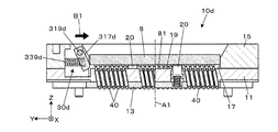
- FIG. 1 is an external view showing a configuration example of the inspection socket 1 of the present embodiment.
- the inspection socket 1 includes a socket body 10, a lid 50, and a pressurizing mechanism 70 as a pressing member.
- the socket body 10 can be taken in and out of the IC package 8 to be inspected, and is attached to the inspection device 9.
- the lid 50 supports the pressurizing mechanism 70 above the socket body 10.
- the pressurizing mechanism 70 is for pressing the inspection target IC package 8 in the lower socket body 10 from above, and applies a load to the inspection target IC package 8.
- the lid 50 is provided with a pair of hooks 60.
- hooks 60 are provided on both the left and right sides.
- the hook 60 is swingably supported by a hook swing shaft 61 along the X-axis direction.
- the hook 60 is a hook swing shaft 61 due to a spring 63.
- the hook 60 on the right side of FIG. 1 is viewed clockwise from the negative X-axis direction, and the hook 60 on the left side of FIG. 1 is viewed from the negative direction of the X-axis. It is urged counterclockwise.
- the hook 60 maintains a state in which the lid 50 covers the upper part of the socket body 10 by engaging the engaging claw 65 with the socket body 10.
- the hook 60 is removed, and the lid 50 is removed from the socket body 10, the inside of the socket body 10 is exposed and the IC package 8 to be inspected can be taken in and out.
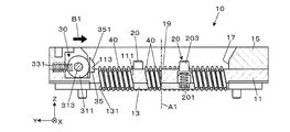
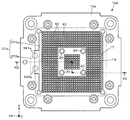
- FIG. 2 is a top view showing a configuration example of the socket body 10.
- FIG. 3 is a cross-sectional view showing a section III-III of FIG.
- FIG. 2 shows the structure of the internal pressing portion 30 by cutting out a part of the guide member 15 (the portion on the left side when facing FIG. 2).
- the socket body 10 includes a pin block 11, a pin plate 13 mounted on the lower surface of the pin block 11, a frame-shaped guide member 15, a pressing portion 30, and an intervening portion.
- the taper member 35 of the above is provided.
- the guide member 15 is placed on the outer peripheral portion of the pin block 11 on the upper surface of the pin block 11.
- the taper member 35 is arranged inside the side portion (left portion in FIG. 2 and the like) of the guide member 15 on the inclined direction side (Y-axis positive direction), which will be described later.
- the pin block 11, the guide member 15, and the taper member 35 form an accommodating recess 17 for accommodating the IC package 8 to be inspected (not shown in FIGS. 2 and 3).
- the IC package 8 to be inspected placed in the storage recess 17 is pushed down from above by the pressurizing mechanism 70, and is housed in a predetermined position of the storage recess 17.
- the pressing portion 30 is for pushing the inspection target IC package 8 accommodated in the accommodating recess 17 in the pressing direction B1.
- the pressing direction B1 is a direction parallel to the negative direction of the Y axis.
- the taper member 35 is interposed between the pressing member 31 and the inspection target IC package 8 when the inspection target IC package 8 is accommodated in the accommodation recess 17.
- the bottom surface of the accommodating recess 17 is a central portion of the upper surface of the pin block 11 and is a portion surrounded by the guide member 15.
- the side wall of the accommodating recess 17 is formed by a guide member 15 and a tapered member 35. Of the side walls of the accommodating recess 17, the three side walls formed by the guide member 15 are fixed, and one side wall formed by the taper member 35 is movable along the Y-axis direction.
- the pin block 11 supports the contact probe 40 on the bottom surface of the accommodating recess 17.
- the contact probe 40 is for conducting the electrode terminal 81 of the IC package 8 to be inspected shown in FIG. 4 or the like with the inspection device 9.
- the electrode terminal 81 is gold, but may be solder.
- the contact probe 40 includes a conductive tube, terminal-side plungers and substrate-side plungers provided at both ends thereof, and a spring provided in the tube. The spring in the tube urges the terminal-side plunger and the substrate-side plunger in a direction away from each other, and the terminal-side plunger and the substrate-side plunger project from both ends of the tube.
- the pin block 11 supports a plurality of contact probes 40 by arranging them along the XY plane so as to correspond to the arrangement of the electrode terminals 81 in the IC package 8 to be inspected. Then, the pin block 11 exposes the upper tip (terminal side plunger) of the contact probe 40 from the exposed surface 19 with the upper surface corresponding to the bottom surface of the accommodating recess 17 as the exposed surface 19.
- the pin block 11 is made of metal.
- the pin block 11 may be made of an insulating resin.
- the pin block 11 has a Z in the central portion thereof in the vertical direction of the exposed surface 19 (the direction parallel to the central axis A1 of the socket body 10 shown by the alternate long and short dash line in FIG. 3). It has a plurality of block-side through holes 111 inclined in a predetermined direction with respect to (axial direction).
- the block-side through hole 111 is a stepped hole having a narrow opening on the upper side (exposed surface 19 side) in order to prevent the contact probe 40 from coming off. Then, by inserting the contact probe 40 into each of the block-side through holes 111, each contact probe 40 is supported in a posture inclined in the above-mentioned predetermined direction (hereinafter, also referred to as “inclination direction”).
- each contact probe 40 The inclination direction of each contact probe 40 is the same.
- a resin material interposed between the pin block 11 and the contact probe 40 is arranged in the vicinity of the opening portion on the upper side (exposed surface 19 side) of the block side through hole 111. With this resin material, the pin block 11 and the contact probe 40 can be brought into a non-contact state.
- the pin block 11 has a plurality of package support portions 20.
- the four package support portions 20 are arranged in the central portion of the pin block 11 so as to avoid the arrangement of the contact probes 40.
- the arrangement position of the package support portion 20 is not limited to the central portion.
- the package support portion 20 includes a spring 201 installed inside the pin block 11 and a spring cap 203 that is placed on the upper portion of the spring 201 and urged upward by the spring 201.
- the pin block 11 is set at a height at which its head (upper end portion of the spring cap 203) protrudes from the exposed surface 19.
- the height of the upper end portion of the spring cap 203 is defined as a height exceeding the tip of the contact probe 40 exposed on the exposed surface 19.
- the pin plate 13 has a plurality of plate-side through holes 131 inclined in the inclination direction at the same inclination angle as the block-side through holes 111 of the pin block 11.
- the plate-side through hole 131 is a stepped hole having a narrow opening on the lower side in order to prevent the contact probe 40 from coming off.
- Each plate-side through-hole 131 corresponds to each of the block-side through-holes 111, and is formed at a position communicating with the corresponding block-side through-hole 111.
- the pin plate 13 penetrates the contact probe 40 inserted into each block-side through-hole 111 through these plate-side through-holes 131, and holds the lower tip (board-side plunger) exposed to the inspection device 9 side. do.
- the pin plate 13 is made of an insulating resin.
- a part of the upper surface of the guide member 15 is a tapered surface inclined toward the accommodating recess 17. Since the guide member 15 has a tapered surface, the IC package 8 to be inspected can be easily taken in and out of the socket body 10.
- the inclination angle of the tapered surface of the guide member 15 can be appropriately set, but it is preferable to set the inclination angle to be the same as that of the tapered surface 351 of the taper member 35.
- the accommodating recess 17 is surrounded by an inclined surface having the same inclination angle, and the IC package 8 to be inspected can be more easily taken in and out of the socket body 10.
- the pressing portion 30 is for pushing the inspection target IC package 8 accommodated in the accommodating recess 17.
- the pressing portion 30 pushes the IC package 8 to be inspected from the side of the accommodating recess 17 in a predetermined pressing direction including a directional component that opposes the inclination direction of the contact probe 40.
- the contact probe 40 is tilted in the positive direction of the Y axis (counterclockwise when viewed from the negative direction of the X axis) with respect to the central axis A1 of the socket body 10. That is, the contact probe 40 is inclined so as to go in the negative direction of the Y axis as it goes in the negative direction of the Z axis. There are a plurality of contact probes 40, all of which are inclined in the same direction.
- the negative direction of the Y-axis, which is opposite to the inclination direction, is defined as the pressing direction B1. Therefore, the pressing portion 30 is installed as a mechanism for pushing the inspection target IC package 8 accommodated in the accommodating recess 17 in the negative direction of the Y axis, which is the pressing direction B1.
- the pressing portion 30 has a pressing member 31 and an elastic member 33 that urges the pressing member 31 in the pressing direction B1.
- the elastic member 33 is elastically deformed by the movement of the pressing member 31 when the IC package 8 to be inspected is accommodated in the accommodating recess 17, and the pressing portion 30 pushes the IC package 8 to be inspected in the pressing direction B1 by the elastic force of the elastic deformation. push.
- the pressing portion 30 pushes the IC package 8 to be inspected in the pressing direction B1 via the taper member 35.
- the pressing member 31 has a roller portion 311 and a support shaft 313 that rotatably supports the roller portion 311.
- the elastic member 33 has a pair of springs 331 and 333 provided at both ends of the support shaft 313 with the inner wall portion of the installation space. Then, the peripheral surface of the roller portion 311 comes into contact with the taper member 35.
- the taper member 35 is a plate body arranged inside the guide member 15 along the side portion on the inclined direction side.
- the tapered member 35 has a tapered surface 351 whose entire upper surface is lowered toward the central portion of the accommodating recess 17. It is sufficient that the accommodation recess 17 has an inclined tapered surface, and a part of the upper surface may be a tapered surface.
- the length of the taper member 35 in the longitudinal direction may exceed the length of the corresponding accommodating recess 17 along the X-axis direction.
- a groove 113 matching the dimensions of the tapered member 35 is formed on the upper surface of the pin block 11.
- the length of the groove portion 113 in the Y-axis direction is wider than the length of the taper member 35 in the Y-axis direction by the movable range C1 pushed and moved by the roller portion 311. Then, the taper member 35 is fitted into the groove portion 113 and is arranged so as to be movable in the Y-axis direction.
- the taper member 35 is provided with a pull-out prevention mechanism (not shown) in order to prevent the taper member 35 from coming off the groove 113 when the IC package 8 to be inspected is attached or detached.
- the taper member 35 is allowed to move along the Y-axis direction between the position in contact with the step in the standard state and the position retracted by the movable range C1 from the position. Therefore, when the IC package 8 to be inspected is put into the socket body 10 and pushed down from above, the taper member 35 moves in the positive direction of the Y axis (the direction opposite to the pressing direction B1), and the IC package 8 to be inspected is accommodated in the recess 17 Is housed in. Then, the IC package 8 to be inspected is in a state of being pushed in the pressing direction B1 from the side in the inclination direction side.
- FIG. 4 and 5 are diagrams for explaining the position change of the pressing portion 30 and the taper member 35 when the IC package 8 to be inspected is accommodated in the accommodating recess 17.
- FIG. 4 shows a cross section III-III of FIG. 2 when the IC package 8 to be inspected is inserted in the socket body 10.
- FIG. 5 shows a cross section III-III of FIG. 2 when the IC package 8 to be inspected is pushed down from above and accommodated in the accommodating recess 17.
- the inspection target IC package 8 is placed on the socket body 10, the inspection target IC package 8 is guided above the accommodating recess 17 by the tapered surface of the guide member 15 and the tapered surface 351 of the taper member 35. Then, it is in a state of being elastically supported by the package support portion 20. Further, in this state, the taper member 35 is pushed by the roller portion 311 by the urging force of the springs 331 and 333 in the pressing direction B1 and is pressed against the step of the groove portion 113.
- the IC package 8 to be inspected receives the elastic force of the springs 331 and 333 in the negative direction of the Y axis via the taper member 35, and is pushed by the pressing portion 30 in the pressing direction B1.
- the end surface (side surface on the negative direction side of the Y axis; the right surface in FIGS. 4 and 5) opposite to the side pressed by the pressing portion 30 of the IC package 8 to be inspected is in contact with the guide member 15. Therefore, the position of the inspection target IC package 8 in the left-right direction (XY plane) is determined, and thereafter, the inspection target IC package 8 only changes its position in the negative direction of the Z axis.
- each contact probe 40 When the IC package 8 to be inspected is further pushed down, the tip (terminal side plunger) of each contact probe 40 exposed from the exposed surface 19 starts to come into contact with the corresponding electrode terminal 81.
- the contact probe 40 can be expanded and contracted in the axial direction (longitudinal direction). Therefore, when the IC package 8 to be inspected is pushed down and the electrode terminal 81 is pressed against the contact probe 40, the contact probe 40 that comes into contact begins to contract.
- the contact probe 40 is arranged so as to be inclined with respect to the direction perpendicular to the exposed surface 19 (Z-axis direction). Further, the position of the IC package 8 to be inspected in the left-right direction (XY plane) is in a fixed state.
- the contact position where the tip of the contact probe 40 is in contact with the electrode terminal 81 of the IC package 8 to be inspected gradually changes according to the descent of the IC package 8 to be inspected (position change in the negative direction of the Z axis).
- the scrubbing operation is performed by scratching the terminal surface.
- a plurality of contact probes 40 can be tilted and supported in a predetermined tilting direction.
- the pressing portion 30 pushes the IC package 8 to be inspected housed in the accommodating recess 17 in the pressing direction B1 including a direction component that opposes the tilting direction of the contact probe 40.
- the tilting direction is a direction tilted in the Y-axis positive direction with respect to the direction perpendicular to the exposed surface 19 (Z-axis direction)
- the pressing direction B1 is the Y-axis which is a directional component against the tilting direction. It was in the negative direction.
- the contact position where the tip of the contact probe 40 is in contact with the electrode terminal 81 of the IC package 8 to be inspected moves in the pressing direction of the IC package 8 to be inspected (position change in the negative Z-axis direction). It changes gradually accordingly.
- FIG. 6 is a diagram showing a configuration example of the socket body 10b in the first modification.
- FIG. 7 is a cross-sectional view showing a cross section of VII-VII of FIG. 6, showing a state in which the IC package 8 to be inspected is pushed down from above and accommodated in the accommodating recess 17.
- FIGS. 6 and 7 the same configurations as those in the above embodiment are designated by the same reference numerals.
- the socket body 10b of the modified example 1 includes a pin block 11, a pin plate 13, a guide member 15, and a pressing portion 30.
- the configuration of the pressing portion 30 is the same as that of the above embodiment, and the roller portion 311 is urged by the springs 331 and 333 in the pressing direction B1 via the support shaft 313.
- the socket body 10b does not include the taper member 35 of the above embodiment.
- the IC package 8 to be inspected When the IC package 8 to be inspected is placed on the socket body 10b and a load is applied to the IC package 8 to be inspected by the pressurizing mechanism 70, the IC package 8 to be inspected is pushed down, the spring 201 contracts, and the package support portion. The support position by 20 is lowered. Then, the roller portion 311 abuts on the side end of the IC package 8 to be inspected and is pushed so as to retract in the positive direction of the Y axis, and the springs 331 and 333 contract. The IC package 8 to be inspected receives the elastic force of the springs 331 and 333 in the negative direction of the Y axis via the roller portion 311 and is pushed by the pressing portion 30 in the pressing direction B1.
- the end surface (side surface on the negative direction side of the Y axis; the right surface in FIGS. 6 and 7) opposite to the side pressed by the pressing portion 30 of the IC package 8 to be inspected is in contact with the guide member 15. Therefore, the position of the inspection target IC package 8 in the left-right direction (XY plane) is determined, and thereafter, the inspection target IC package 8 only changes its position in the negative direction of the Z axis.
- each contact probe 40 When the IC package 8 to be inspected is further pushed down, the tip (terminal side plunger) of each contact probe 40 exposed from the exposed surface 19 starts to come into contact with the corresponding electrode terminal 81.
- the contact probe 40 can be expanded and contracted in the axial direction (longitudinal direction). Therefore, when the IC package 8 to be inspected is pushed down and the electrode terminal 81 is pressed against the contact probe 40, the contact probe 40 that comes into contact begins to contract.
- the contact probe 40 is arranged so as to be inclined with respect to the direction perpendicular to the exposed surface 19 (Z-axis direction). Further, the position of the IC package 8 to be inspected in the left-right direction (XY plane) is in a fixed state.
- the contact position where the tip of the contact probe 40 is in contact with the electrode terminal 81 of the IC package 8 to be inspected gradually changes according to the descent of the IC package 8 to be inspected (position change in the negative direction of the Z axis).
- the scrubbing operation is performed by scratching the terminal surface.
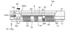
- FIG. 8 is a diagram showing a configuration example of the socket body 10c in the modified example 2.
- FIG. 9 is a cross-sectional view showing the IX-IX cross section of FIG. 8, showing a state in which the IC package 8 to be inspected is pushed down from above and housed in the storage recess 17.
- FIGS. 8 and 9 the same configurations as those in the above embodiment are designated by the same reference numerals.
- the socket body 10c of the modified example 2 includes a pin block 11, a pin plate 13, a guide member 15, and a pressing portion 30c.
- the pressing portion 30c has a tapered member 32c as a pressing member instead of the roller portion 311 of the first modification.
- the pressing portion 30c has a pair of springs 335c and 337c provided between the tapered member 32c and the inner wall portion of the installation space thereof as an elastic member for urging the tapered member 32c in the pressing direction B1.
- the taper member 32c has a long plate-shaped portion 321c as a whole along the X-axis direction.
- the central portion of the plate-shaped portion 321c in the longitudinal direction has a wide shape.
- the plate-shaped portion 321c forms a part of the side wall of the accommodating recess 17.
- the tapered member 32c has a tapered surface 323c in which a part of the upper surface of the plate-shaped portion 321c is lowered toward the central portion of the accommodating recess 17. It should be noted that the entire upper surface may be a tapered surface.
- the IC package 8 to be inspected When the IC package 8 to be inspected is placed in the socket body 10c and a load is applied to the IC package 8 to be inspected by the pressurizing mechanism 70, the IC package 8 to be inspected is pushed down, the spring 201 contracts, and the package support portion. The support position by 20 is lowered. Then, the plate-shaped portion 321c of the taper member 32c abuts on the side end of the IC package 8 to be inspected and is pushed so as to retract in the positive direction of the Y axis, and the springs 335c and 337c are contracted by the retracting taper member 32c.
- the IC package 8 to be inspected receives the elastic force of the springs 335c and 337c in the negative direction of the Y axis, and is pushed by the pressing portion 30c in the pressing direction B1.
- the end surface (side surface on the negative direction side of the Y axis; right side surface in FIGS. 8 and 9) opposite to the side pressed by the pressing portion 30c of the IC package 8 to be inspected is in contact with the guide member 15. Therefore, the position of the inspection target IC package 8 in the left-right direction (XY plane) is determined, and thereafter, the inspection target IC package 8 only changes its position in the negative direction of the Z axis.
- each contact probe 40 When the IC package 8 to be inspected is further pushed down, the tip (terminal side plunger) of each contact probe 40 exposed from the exposed surface 19 starts to come into contact with the corresponding electrode terminal 81.
- the contact probe 40 can be expanded and contracted in the axial direction (longitudinal direction). Therefore, when the IC package 8 to be inspected is pushed down and the electrode terminal 81 is pressed against the contact probe 40, the contact probe 40 that comes into contact begins to contract.
- the contact probe 40 is arranged so as to be inclined with respect to the direction perpendicular to the exposed surface 19 (Z-axis direction). Further, the position of the IC package 8 to be inspected in the left-right direction (XY plane) is in a fixed state.
- the contact position where the tip of the contact probe 40 is in contact with the electrode terminal 81 of the IC package 8 to be inspected gradually changes according to the descent of the IC package 8 to be inspected (position change in the negative direction of the Z axis).
- the scrubbing operation is performed by scratching the terminal surface.
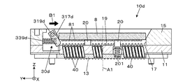
- FIGS. 10 and 11 are vertical cross-sectional views showing a configuration example of the socket body 10d in the modified example 3, and show a change in the pressing portion 30d when the IC package 8 to be inspected is housed in the housing recess 17.
- FIG. 10 shows a state in which the IC package 8 to be inspected is inserted in the socket body 10d.
- FIG. 11 shows a state in which the IC package 8 to be inspected is pushed down from above and housed in the storage recess 17.
- FIGS. 10 and 11 the same reference numerals are given to the same configurations as those in the above embodiment.
- the socket body 10d of the modified example 3 includes a pin block 11, a pin plate 13, a guide member 15, and a pressing portion 30d.
- the pressing portion 30d has a rocking body 317d that is swingably supported by a rocking shaft 319d along the X-axis direction as a pressing member. Further, the pressing portion 30d has a spring 339d as an elastic member that urges the rocking body 317d in the pressing direction B1.
- the spring 339d is arranged in a movable space of the rocking body 317d provided in the side wall of the accommodating recess 17 in a posture of urging the rocking body 317d in the pressing direction B1.
- the rocking body 317d is arranged in a posture inclined at an angle similar to the tapered surface of the guide member 15 in a natural state in which the IC package 8 to be inspected is not placed.
- the IC package 8 to be inspected When the IC package 8 to be inspected is placed on the socket body 10d, the IC package 8 to be inspected is guided above the accommodating recess 17 by the tapered surface of the guide member 15 and the inclined surface of the rocking body 317d, and is elastic by the package support portion 20. It will be in a supported state (state in FIG. 10).
- the IC package 8 to be inspected is pushed down, the spring 201 contracts, and the support position by the package support portion 20 is lowered. Then, the rocking body 317d comes into contact with the side end of the IC package 8 to be inspected, rotates clockwise with respect to the swinging shaft 319d in the negative direction of the X axis, and contracts the spring 339d.
- the IC package 8 to be inspected receives the elastic force of the contracted spring 339d in the negative direction of the Y axis, and is pushed by the pressing portion 30d in the pressing direction B1.
- the end surface (side surface on the negative direction side of the Y axis; right side surface in FIGS. 10 and 11) opposite to the side pressed by the pressing portion 30d of the IC package 8 to be inspected is in contact with the guide member 15. Therefore, the position of the inspection target IC package 8 in the left-right direction (XY plane) is determined, and thereafter, the inspection target IC package 8 only changes its position in the negative direction of the Z axis.
- each contact probe 40 When the IC package 8 to be inspected is further pushed down, the tip (terminal side plunger) of each contact probe 40 exposed from the exposed surface 19 starts to come into contact with the corresponding electrode terminal 81.
- the contact probe 40 can be expanded and contracted in the axial direction (longitudinal direction). Therefore, when the IC package 8 to be inspected is pushed down and the electrode terminal 81 is pressed against the contact probe 40, the contact probe 40 that comes into contact begins to contract.
- the contact probe 40 is arranged so as to be inclined with respect to the direction perpendicular to the exposed surface 19 (Z-axis direction). Further, the position of the IC package 8 to be inspected in the left-right direction (XY plane) is in a fixed state.
- the contact position where the tip of the contact probe 40 is in contact with the electrode terminal 81 of the IC package 8 to be inspected gradually changes according to the descent of the IC package 8 to be inspected (position change in the negative direction of the Z axis).
- the scrubbing operation is performed by scratching the terminal surface.
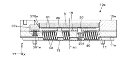
- FIG. 12 is a diagram showing a configuration example of the socket body 10e in the modified example 4.
- 13 and 14 are cross-sectional views showing a cross section of XIII-XIII of FIG.
- FIG. 13 shows a state in which the IC package 8 to be inspected is inserted in the socket body 10e.
- FIG. 14 shows a state in which the IC package 8 to be inspected is pushed down from above and housed in the storage recess 17.
- the same configurations as those in the above embodiment are designated by the same reference numerals.
- the socket body 10e of the modified example 4 is an elastic member that urges the pin block 11e, the pin plate 13, the guide member 15e, the taper member 37e, and the taper member 37e upward.
- a pair of springs 391e and 393e are provided.
- the taper member 37e has a long plate-shaped portion 371e as a whole along the X-axis direction.
- the central portion of the plate-shaped portion 371e in the longitudinal direction has a wide shape.
- the plate-shaped portion 371e forms a part of the side wall of the accommodating recess 17.
- the taper member 37e is supported so as to be displaceable in the vertical direction by two springs 391e and 393e that urge the taper member 37e upward.
- the taper member 37e has a tapered surface 375e in which a part of the upper surface of the plate-shaped portion 371e is lowered toward the bottom surface of the accommodating recess 17.
- One end of the springs 391e and 393e is installed inside the wide portion 373e, and the other end is installed inside the pin block 11e below it.
- the IC package 8 to be inspected When the IC package 8 to be inspected is placed on the socket body 10e, the IC package 8 to be inspected is guided above the accommodating recess 17 by the tapered surface of the guide member 15e and the tapered surface 375e of the tapered member 37e, and is guided by the package support portion 20. It is in an elastically supported state (the state shown in FIG. 13).
- the IC package 8 to be inspected is pushed down, the spring 201 contracts, and the support position by the package support portion 20 is lowered. Then, the IC package 8 to be inspected moves along the tapered surface 375e of the tapered member 37e. Therefore, the IC package 8 to be inspected tends to move in the negative Z-axis direction and the negative Y-axis along the inclined surface of the tapered surface 375e.
- the end surface side surface on the negative direction side of the Y axis; the right surface in FIGS.
- the position of the inspection target IC package 8 in the left-right direction (XY plane) is determined, and thereafter, the inspection target IC package 8 only changes its position in the negative direction of the Z axis.
- each contact probe 40 When the IC package 8 to be inspected is further pushed down, the tip (terminal side plunger) of each contact probe 40 exposed from the exposed surface 19 starts to come into contact with the corresponding electrode terminal 81.
- the contact probe 40 can be expanded and contracted in the axial direction (longitudinal direction). Therefore, when the IC package 8 to be inspected is pushed down and the electrode terminal 81 is pressed against the contact probe 40, the contact probe 40 that comes into contact begins to contract.
- the contact probe 40 is arranged so as to be inclined with respect to the direction perpendicular to the exposed surface 19 (Z-axis direction). Further, the position of the IC package 8 to be inspected in the left-right direction (XY plane) is in a fixed state.
- the contact position where the tip of the contact probe 40 is in contact with the electrode terminal 81 of the IC package 8 to be inspected gradually changes according to the descent of the IC package 8 to be inspected (position change in the negative direction of the Z axis).
- the scrubbing operation is performed by scratching the terminal surface.
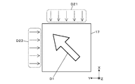
- Modification 5 In the above-described embodiment and each modification, a configuration in which the IC package to be inspected is pushed in one direction is illustrated. On the other hand, depending on the tilting direction of the contact probe, the IC package to be inspected may be pushed in a plurality of directions.
- FIG. 15 is a schematic view showing the relationship between the tilting direction of the contact probe supported at the bottom of the accommodating recess 17 and the pushing direction of the IC package to be inspected.
- FIG. 15 is a top view of the accommodating recess 17 as in FIGS. 2, 6, 8 and 12.
- the X-axis direction, Y-axis direction, and Z-axis direction are the same as the directions shown in other drawings.
- the inclination direction of the contact probe was the left direction (Y-axis positive direction) with respect to the drawing, but in the present modification 5, as shown by the arrow D1, the contact probe is oriented toward FIG. It is diagonally upward to the left (X-axis positive direction and Y-axis positive direction).
- the IC package to be inspected is pushed in the direction D21 (X-axis negative direction) and the direction D23 (Y-axis negative direction), which are the directions including the direction component opposite to the inclination direction D1.
- any of the pressing portions 30, 30c, and 30d shown in the above-described embodiment and the modified examples 1 to 3 is installed on the X-axis positive direction side and the Y-axis positive direction side.
- the types of pressing portions installed on the positive direction side of the X axis and the positive direction side of the Y axis may be different.
- the IC package 8 to be inspected is pushed in the direction D21 (negative X-axis direction) and in the direction D23 (negative Y-axis).
- the taper members 37e and the springs 391e and 393e of the modified example 4 may be installed on the X-axis positive direction side and the Y-axis positive direction side, and the IC package to be inspected may be pushed in the directions D21 and D23.
- An aspect of the present disclosure is an inspection in which a pin block that exposes the tip of a contact probe from an exposed surface and supports the contact probe by inclining it in a predetermined direction with respect to a direction perpendicular to the exposed surface, and contacting the contact probe.
- An inspection socket including a pressing portion for pushing the target IC package.
- the pin block can support the contact probe by inclining it in a predetermined direction.
- the IC package to be inspected can be pushed by the pressing portion. Since the pin block is tilted in a predetermined direction, when the contact probe comes into contact with the electrode terminal of the IC package to be inspected, the IC package to be inspected moves based on the tilt direction of the contact probe, and scrubbing operation is unlikely to occur. May occur. However, since the IC package to be inspected is pushed by the pressing portion, such a situation can be suppressed, and a stable scrub operation can be performed when the contact probe and the electrode terminal of the IC package to be inspected come into contact with each other.
- each contact probe since the inclination direction of each contact probe may be the same, it is not necessary to increase the size of the pin block, and complicated processing is not required for the pin block that supports the contact probe. Further, since the IC package to be inspected is pushed by the pressing portion, the positioning accuracy of the IC package to be inspected can be improved as compared with the case where there is no pressing portion.
- the pressing portion may push the IC package to be inspected in a pressing direction including a directional component that opposes the predetermined direction.
- the pressing direction may be a direction parallel to the plate surface of the IC package to be inspected.
- the IC package to be inspected is pressurized in the direction perpendicular to the plate surface of the IC package to be inspected. Since the pressing direction is parallel to the plate surface of the IC package to be inspected, the pressing direction and the pressing direction can be different directions. Therefore, the IC package itself to be inspected is less likely to be damaged as compared with the case where the pressing direction and the pressing direction are parallel to each other.
- the pressing portion may have a pressing member and an elastic member that urges the pressing member.
- the pressing member may have a roller portion.
- the roller unit can push the IC package to be inspected, and the IC package to be inspected can be prevented from being damaged.
- the urging direction of the elastic member and the pressing direction may be parallel.
- An intervening portion may be provided, and the pressing portion may push the IC package to be inspected through the intervening portion.
- the pressing portion Since the IC package to be inspected can be pushed through the intervening portion, the pressing portion does not directly push the IC package to be inspected, and damage to the IC package to be inspected can be prevented.
- the intervening portion may have a tapered surface.
- the contact probe and the electrode terminal of the IC package to be inspected are brought into contact with each other, the IC package to be inspected can be moved along the tapered surface, so that the IC package to be inspected can be easily replaced.
Landscapes
- Physics & Mathematics (AREA)
- General Physics & Mathematics (AREA)
- Engineering & Computer Science (AREA)
- Computer Hardware Design (AREA)
- Microelectronics & Electronic Packaging (AREA)
- Condensed Matter Physics & Semiconductors (AREA)
- Power Engineering (AREA)
- Testing Of Individual Semiconductor Devices (AREA)
- Measuring Leads Or Probes (AREA)
- Connecting Device With Holders (AREA)
Abstract
コンタクトプローブ(40)の先端を露出面(19)から露出させ、前記コンタクトプローブ(40)を前記露出面に垂直な方向に対して所定方向に傾斜させて支持するピンブロック(11)と、前記コンタクトプローブ(40)と接触する検査対象ICパッケージ(8)を押す押し付け部(30)と、を備える検査用ソケット(1)である。
Description
本発明は、検査用ソケットに関する。
従来から、性能試験等のICパッケージの検査に用いられる検査用ソケットが知られている。検査用ソケットは、検査対象ICパッケージを検査装置と電気的に接続するためのものであり、当該検査対象ICパッケージの電極端子の配置に対応させて配列した複数のコンタクトプローブを備えている。
この種の検査用ソケットとして、電極端子に対して斜めに接触するようにコンタクトプローブを傾斜させたものも知られている(特許文献1を参照)。特許文献1では、複数のコンタクトプローブの配列が対称となるように、当該配列の中心を境に各コンタクトプローブの傾斜方向を逆向きにしている。これは、電極端子にコンタクトプローブを接触させる際、検査対象ICパッケージが電極端子の配置と平行な方向に移動せずに、端子表面を引っかくスクラブ動作を確実に行わせるためである。スクラブ動作を行わせることで、端子表面に酸化膜や汚れ等があってもその下の電極端子に確実にコンタクトプローブの先端を接触させることができ、両者の導通を確保することができる。
しかし、特許文献1の構成では、各コンタクトプローブを支持する支持部において、コンタクトプローブの支持孔(段付き孔)を異なる方向に傾斜させて形成する必要が生じる。このことは、検査用ソケットの大型化や、支持部の加工の複雑化を招き、コスト増となる。また、検査対象ICパッケージにおける電極端子の配置や数によっては、コンタクトプローブを対称に配列するのが困難な場合もある。
本発明の目的の一例は、コンタクトプローブと検査対象ICパッケージの電極端子との接触時に安定してスクラブ動作を行わせることである。
本発明の態様は、コンタクトプローブの先端を露出面から露出させ、前記コンタクトプローブを前記露出面に垂直な方向に対して所定方向に傾斜させて支持するピンブロックと、前記コンタクトプローブと接触する検査対象ICパッケージを押す押し付け部と、を備える検査用ソケットである。
この態様によれば、ピンブロックは、コンタクトプローブを所定方向に傾斜させて支持することができる。また、検査対象ICパッケージを、押し付け部により押すことができる。ピンブロックが所定方向に傾斜しているので、コンタクトプローブと検査対象ICパッケージの電極端子との接触時に、コンタクトプローブの傾斜方向に基づいて検査対象ICパッケージが移動し、スクラブ動作が発生し難い事態が生じる可能性がある。しかし、検査対象ICパッケージが押し付け部により押されているので、このような事態を抑制し、コンタクトプローブと検査対象ICパッケージの電極端子との接触時に安定してスクラブ動作を行うことができる。また、各コンタクトプローブの傾斜の方向は同じでよいので、ピンブロックを大型化する必要は無く、コンタクトプローブを支持するピンブロックに対して複雑な加工が不要となる。また、押し付け部により検査対象ICパッケージを押すので、押し付け部が無い場合に比べて、検査対象ICパッケージの位置決め精度を上げることができる。
以下、本発明の好適な実施形態の例を説明するが、本発明を適用可能な形態は以下の実施形態に限定されない。本実施形態の説明において、検査用ソケット1の上下方向は、蓋体50を閉じる方向を下方向とし、蓋体50を開ける方向を上方向とする。検査用ソケット1は、下方向を、重力による鉛直下向きの方向に向けて使用される。このため、検査対象ICパッケージ8が検査用ソケット1内に置かれると、後述する通り、その自重により検査用ソケット1内のパッケージ支持部20上に載置された状態となる。各図においては、上下方向をZ軸方向とし、これに垂直なX軸方向およびY軸方向を共通に定めた右手系の直交三軸を、共通する方向として示す。Z軸正方向が上方向、Z軸負方向が下方向である。図1の紙面に向かって手前から奥に向かう方向がX軸正方向、奥から手前に向かう方向がX軸負方向である。X軸方向とZ軸方向に直交する図1の左右方向の右から左へ向かう方向がY軸正方向、左から右へ向かう方向がY軸負方向である。
図1は、本実施形態の検査用ソケット1の構成例を示す外観図である。図1に示すように、検査用ソケット1は、ソケット本体10と、蓋体50と、押さえ部材としての加圧機構70とを備える。
ソケット本体10は、検査対象ICパッケージ8の出し入れが可能であり、検査装置9に装着される。蓋体50は、ソケット本体10の上方において加圧機構70を支持する。加圧機構70は、下方のソケット本体10内の検査対象ICパッケージ8を上方から押さえるためのものであり、当該検査対象ICパッケージ8に対して荷重を付与する。
蓋体50には、一対のフック60が設けられている。図1の例では、左右両側にそれぞれフック60が設けられている。フック60は、X軸方向に沿ったフック揺動軸61で揺動可能に支持される。フック60は、スプリング63によって、フック揺動軸61で、図1の右側のフック60はX軸負方向から見て時計回り方向へ、図1の左側のフック60はX軸負方向から見て反時計回り方向へ付勢されている。
フック60は、係合爪65がソケット本体10と係合することで、蓋体50がソケット本体10の上方を覆う状態を維持する。スプリング63による付勢状態を解除してフック60を外し、蓋体50をソケット本体10から取り外すと、ソケット本体10の内部が露出されて、検査対象ICパッケージ8の出し入れが可能となる。
図2は、ソケット本体10の構成例を示す上面図である。図3は、図2のIII-III断面を示す断面図である。図2では、ガイド部材15の一部(図2に向かって左側部)を切り欠いて、内部の押し付け部30の構造を示している。
図2および図3に示すように、ソケット本体10は、ピンブロック11と、ピンブロック11の下面に装着されたピンプレート13と、枠状のガイド部材15と、押し付け部30と、介在部としてのテーパー部材35とを備える。ガイド部材15は、ピンブロック11の上面においてピンブロック11の外周部分に載置されている。テーパー部材35は、ガイド部材15の後述する傾斜方向側(Y軸正方向)の側部(図2等では左側部)の内側に配置されている。ピンブロック11と、ガイド部材15と、テーパー部材35とが検査対象ICパッケージ8(図2および図3では不図示)を収容する収容凹部17を形成する。この収容凹部17に載置された検査対象ICパッケージ8は、加圧機構70によって上方から押し下げられることで、収容凹部17の所定位置に収容される。押し付け部30は、収容凹部17に収容される検査対象ICパッケージ8を押し付け方向B1に押すためのものである。押し付け方向B1は、Y軸負方向に平行な方向である。テーパー部材35は、収容凹部17への検査対象ICパッケージ8の収容時において、押圧部材31と検査対象ICパッケージ8との間に介在する。
収容凹部17の底面は、ピンブロック11の上面の中央部分であって、ガイド部材15によって囲まれる部分である。収容凹部17の側壁は、ガイド部材15とテーパー部材35とによって形成される。そして、収容凹部17の側壁のうち、ガイド部材15によって形成される三方の側壁は固定とされ、テーパー部材35によって形成される一方の側壁はY軸方向に沿って移動可能となっている。
ピンブロック11は、収容凹部17の底面においてコンタクトプローブ40を支持する。コンタクトプローブ40は、図4等に示す検査対象ICパッケージ8の電極端子81を検査装置9と導通させるためのものである。電極端子81は金であるが、半田であってもよい。コンタクトプローブ40は、導電性のチューブと、その両端にそれぞれ設けられる端子側プランジャおよび基板側プランジャと、チューブ内に設けられるスプリングとを具備して構成される。チューブ内のスプリングは端子側プランジャと基板側プランジャとを互いに離間する方向へと付勢し、端子側プランジャおよび基板側プランジャは、チューブの両端からそれぞれ突出している。
ピンブロック11の説明に戻る。本実施形態では、ピンブロック11は、検査対象ICパッケージ8における電極端子81の配置に対応するように、複数のコンタクトプローブ40をXY平面に沿って配列して支持する。そして、ピンブロック11は、収容凹部17の底面に相当する上面を露出面19として、当該露出面19からコンタクトプローブ40の上側の先端(端子側プランジャ)を露出させる。このピンブロック11は、金属で作られる。ピンブロック11は、絶縁性の樹脂で作られてもよい。
より詳細には、ピンブロック11は、図3に示すように、その中央部分において、露出面19の垂直方向(図3中に一点鎖線で示すソケット本体10の中心軸A1に平行な方向、Z軸方向)に対して所定方向に傾斜した複数のブロック側貫通孔111を有する。ブロック側貫通孔111は、コンタクトプローブ40の抜け防止のため、上側(露出面19側)の開口部分が細い段付き孔である。そして、各ブロック側貫通孔111のそれぞれにコンタクトプローブ40が挿入されることで、前述の所定方向(以下「傾斜方向」ともいう)に傾斜させた姿勢で各コンタクトプローブ40を支持する。各コンタクトプローブ40の傾斜方向は同じである。ピンブロック11が金属製の場合には、ブロック側貫通孔111の上側(露出面19側)の開口部分近傍において、ピンブロック11とコンタクトプローブ40との間に介在する樹脂材が配置される。この樹脂材により、ピンブロック11とコンタクトプローブ40とを非接触の状態にすることができる。
ピンブロック11は、複数のパッケージ支持部20を有する。本実施形態では、4つのパッケージ支持部20が、ピンブロック11の中央部分においてコンタクトプローブ40の配列を避けて配置されている。ただし、パッケージ支持部20の配置位置は、中央部分に限定されるものではない。
パッケージ支持部20は、ピンブロック11の内部に設置されたスプリング201と、当該スプリング201の上部に被せられ、当該スプリング201によって上方に付勢されたスプリングキャップ203とを備える。ピンブロック11は、その頭部(スプリングキャップ203の上端部)が露出面19から突出する高さに設定される。具体的には、スプリングキャップ203の上端部の高さは、図3に示すように、露出面19に露出しているコンタクトプローブ40の先端を超える高さに規定される。ソケット本体10に入れられた検査対象ICパッケージ8を、コンタクトプローブ40の上方において端子側プランジャとは非接触の状態で保持することができる(図4を参照)。
ピンプレート13は、ピンブロック11のブロック側貫通孔111と同じ傾斜角度で傾斜方向に傾斜した複数のプレート側貫通孔131を有する。プレート側貫通孔131は、コンタクトプローブ40の抜け防止のため、下側の開口部分が細い段付き孔である。各プレート側貫通孔131は、各ブロック側貫通孔111のそれぞれと対応しており、対応するブロック側貫通孔111と連通する位置に形成される。ピンプレート13は、これらプレート側貫通孔131によって各ブロック側貫通孔111に挿入されたコンタクトプローブ40を貫通させ、その下側の先端(基板側プランジャ)を検査装置9側へと露出させて保持する。ピンプレート13は、絶縁性の樹脂で作られる。
ガイド部材15は、上面の一部が、収容凹部17側に傾斜したテーパー面とされている。ガイド部材15がテーパー面を有しているため、ソケット本体10への検査対象ICパッケージ8の出し入れが行いやすくなる。ガイド部材15のテーパー面の傾斜角度は適宜設定することができるが、テーパー部材35のテーパー面351と同じ傾斜角度に設定すると好適である。これにより、収容凹部17は、同じ傾斜角度の傾斜面で取り囲まれるようになり、ソケット本体10への検査対象ICパッケージ8の出し入れがより行いやすくなる。
押し付け部30は、収容凹部17に収容される検査対象ICパッケージ8を押すためのものである。押し付け部30は、収容凹部17の側方から、コンタクトプローブ40の傾斜方向に逆らう方向成分を含む所定の押し付け方向へと検査対象ICパッケージ8を押す。
コンタクトプローブ40は、ソケット本体10の中心軸A1に対して、上面視においてY軸正方向(X軸負方向から見て反時計回り)に傾斜している。すなわち、コンタクトプローブ40は、Z軸負方向に向かうに連れてY軸負方向に向かうような傾斜をしている。コンタクトプローブ40は複数あり、全て同じ方向に傾斜している。この傾斜方向と逆らう逆向きのY軸負方向を、押し付け方向B1としている。そのため、押し付け部30は、収容凹部17に収容される検査対象ICパッケージ8を、押し付け方向B1であるY軸負方向へと押す機構として設置される。
押し付け部30は、押圧部材31と、当該押圧部材31を押し付け方向B1に付勢する弾性部材33とを有する。検査対象ICパッケージ8の収容凹部17への収容時に押圧部材31が移動することで弾性部材33が弾性変形し、当該弾性変形の弾性力によって押し付け部30が検査対象ICパッケージ8を押し付け方向B1に押す。押し付け部30は、テーパー部材35を介して検査対象ICパッケージ8を押し付け方向B1に押す。
押圧部材31は、ローラー部311と、ローラー部311を回動可能に支持する支持軸313とを有する。弾性部材33は、支持軸313の両端部において設置空間の内壁部との間に設けられた一対のスプリング331,333を有する。そして、ローラー部311の周面が、テーパー部材35と当接する。
テーパー部材35は、ガイド部材15の傾斜方向側の側部に沿ってその内側に配置された板体である。テーパー部材35は、上面の全部が収容凹部17の中央部分に向けて低下するテーパー面351とされている。なお、収容凹部17側に傾斜したテーパー面を有していればよく、上面の一部がテーパー面とされた構成でもよい。テーパー部材35の長手方向の長さ(X軸方向に沿った長さ)は、対応する収容凹部17のX軸方向に沿った長さを超える長さであってもよい。一方で、ピンブロック11の上面には、テーパー部材35の寸法に合わせた溝部113が形成されている。溝部113のY軸方向の長さは、テーパー部材35のY軸方向の長さよりも、ローラー部311によって押されて移動する可動範囲C1の分だけ広い。そして、テーパー部材35は、この溝部113に嵌め込まれて、Y軸方向に移動自在に配置される。なお、テーパー部材35は、検査対象ICパッケージ8の脱着時等に溝部113から外れるのを防止するため、不図示の抜け防止機構を備えている。
したがって、収容凹部17に検査対象ICパッケージ8が収容されていないときには、テーパー部材35は、スプリング331,333による支持軸313に対する押し付け方向B1への付勢力によってローラー部311に押され、その下端が溝部113の段差に当接する。この状態が標準状態である。図2および図3では、この押し付け部30およびテーパー部材35の標準状態を示しており、収容凹部17に検査対象ICパッケージ8が収容されていないときの状態を示している。一方で、テーパー部材35は、当該標準状態における段差に当接した位置と、そこから可動範囲C1の分後退した位置との間でY軸方向に沿った移動が許容される。よって、検査対象ICパッケージ8がソケット本体10に入れられて上方から押し下げられたときには、テーパー部材35がY軸正方向(押し付け方向B1の逆方向)に動いて検査対象ICパッケージ8が収容凹部17に収容される。そして、検査対象ICパッケージ8は、傾斜方向側の側方から押し付け方向B1に押された状態となる。
図4および図5は、検査対象ICパッケージ8が収容凹部17へと収容される際の押し付け部30およびテーパー部材35の位置変化を説明するための図である。図4は、ソケット本体10に検査対象ICパッケージ8が入れられたときの図2のIII-III断面を示す。図5は、当該検査対象ICパッケージ8が上方から押し下げられて収容凹部17に収容されたときの図2のIII-III断面を示している。
図4に示すように、ソケット本体10に検査対象ICパッケージ8が置かれると、検査対象ICパッケージ8は、ガイド部材15のテーパー面やテーパー部材35のテーパー面351によって収容凹部17の上方に導かれ、パッケージ支持部20によって弾性支持された状態となる。また、この状態では、テーパー部材35は、スプリング331,333による押し付け方向B1への付勢力によってローラー部311に押され、溝部113の段差に押し付けられている。
その後、加圧機構70によって検査対象ICパッケージ8に荷重が付与されると、図5に示すように、検査対象ICパッケージ8が押し下げられ、スプリング201が収縮してパッケージ支持部20による支持位置が降下する。すると、テーパー部材35が検査対象ICパッケージ8の側端に当接して、テーパー部材35がY軸正方向に後退するように押される。後退するテーパー部材35によって押されたローラー部311がY軸正方向に後退するように移動し、スプリング331,333が収縮する。検査対象ICパッケージ8は、テーパー部材35を介してスプリング331,333の弾性力をY軸負方向に受け、押し付け部30によって押し付け方向B1に押された状態となる。検査対象ICパッケージ8の押し付け部30によって押される側とは反対側の端面(Y軸負方向側の側面;図4,5において右側面)は、ガイド部材15に当接した状態となる。したがって、検査対象ICパッケージ8の左右方向(XY平面)の位置が決まった状態となり、これ以降、検査対象ICパッケージ8はZ軸負方向へ位置変化するだけとなる。
検査対象ICパッケージ8が更に押し下げられると、露出面19から露出している各コンタクトプローブ40の先端(端子側プランジャ)がそれぞれ対応する電極端子81と接触し始める。コンタクトプローブ40は、軸方向(長手方向)に伸縮可能である。そのため、検査対象ICパッケージ8が押し下げられて、電極端子81がコンタクトプローブ40に押し当てられると、接触したコンタクトプローブ40が収縮し始める。但し、コンタクトプローブ40は、露出面19に垂直な方向(Z軸方向)に対して傾斜して配置されている。また、検査対象ICパッケージ8の左右方向(XY平面)の位置は決まった状態である。したがって、コンタクトプローブ40の先端が検査対象ICパッケージ8の電極端子81に接触している接触位置は、検査対象ICパッケージ8の降下(Z軸負方向への位置変化)に応じて徐々に変化し、端子表面を引っかくスクラブ動作が行われる。
以上説明したように、本実施形態の検査用ソケット1によれば、複数のコンタクトプローブ40を所定の傾斜方向へと傾斜させて支持することができる。また、押し付け部30が、収容凹部17に収容される検査対象ICパッケージ8を、コンタクトプローブ40の傾斜方向に逆らう方向成分を含む押し付け方向B1に押す。本実施形態では、傾斜方向を、露出面19に垂直な方向(Z軸方向)に対してY軸正方向に傾けた方向とし、押し付け方向B1は、その傾斜方向に逆らう方向成分であるY軸負方向とした。全てのコンタクトプローブ40の傾斜方向を同じとしたため、検査対象ICパッケージ8をコンタクトプローブ40に押し当てる際には、検査対象ICパッケージ8に対して、その傾斜方向に沿った方向(本実施形態ではY軸正方向)に移動させようとする力が働き、Y軸正方向に動きかねない。しかし、傾斜方向に逆らう方向成分を含む押し付け方向B1から、検査対象ICパッケージ8に押し付け力が加わっているため、Y軸正方向への動きが抑止される。この結果、コンタクトプローブ40の先端が検査対象ICパッケージ8の電極端子81に接触している接触位置が、検査対象ICパッケージ8の押し当て方向への移動(Z軸負方向への位置変化)に応じて徐々に変化する。
したがって、コンタクトプローブ40を電極端子81に押し当てる際の検査対象ICパッケージ8の押し当て方向(本実施形態ではZ軸負方向)以外への移動を防止でき、安定したスクラブ動作を行わせることが可能となる。
なお、本発明を適用可能な形態は上記した実施形態に限定されるものではなく、適宜構成要素の追加・省略・変更を施すことができる。
(変形例1)
例えば、上記実施形態では、テーパー部材35を介して収容凹部に収容される検査対象ICパッケージ8を押す構成について説明した。これに対し、押し付け部30が直接検査対象ICパッケージ8を押す構成としてもよい。図6は、変形例1におけるソケット本体10bの構成例を示す図である。図7は、図6のVII-VII断面を示す断面図であり、検査対象ICパッケージ8が上方から押し下げられて収容凹部17に収容された状態を示している。図6および図7では、上記実施形態と同様の構成には同一の符号を付して示している。
例えば、上記実施形態では、テーパー部材35を介して収容凹部に収容される検査対象ICパッケージ8を押す構成について説明した。これに対し、押し付け部30が直接検査対象ICパッケージ8を押す構成としてもよい。図6は、変形例1におけるソケット本体10bの構成例を示す図である。図7は、図6のVII-VII断面を示す断面図であり、検査対象ICパッケージ8が上方から押し下げられて収容凹部17に収容された状態を示している。図6および図7では、上記実施形態と同様の構成には同一の符号を付して示している。
図6および図7に示すように、変形例1のソケット本体10bは、ピンブロック11と、ピンプレート13と、ガイド部材15と、押し付け部30とを備える。押し付け部30の構成は上記実施形態と同様であり、ローラー部311は、スプリング331,333によって支持軸313を介して押し付け方向B1に付勢される。ソケット本体10bは、上記実施形態のテーパー部材35を備えていない。
検査対象ICパッケージ8がソケット本体10bに置かれ、加圧機構70によって当該検査対象ICパッケージ8に荷重が付与されると、検査対象ICパッケージ8が押し下げられ、スプリング201が収縮してパッケージ支持部20による支持位置が降下する。すると、ローラー部311が検査対象ICパッケージ8の側端に当接してY軸正方向に後退するように押されて、スプリング331,333が収縮する。検査対象ICパッケージ8は、ローラー部311を介してスプリング331,333の弾性力をY軸負方向に受け、押し付け部30によって押し付け方向B1に押された状態となる。検査対象ICパッケージ8の押し付け部30によって押される側とは反対側の端面(Y軸負方向側の側面;図6,7において右側面)は、ガイド部材15に当接した状態となる。したがって、検査対象ICパッケージ8の左右方向(XY平面)の位置が決まった状態となり、これ以降、検査対象ICパッケージ8はZ軸負方向へ位置変化するだけとなる。
検査対象ICパッケージ8が更に押し下げられると、露出面19から露出している各コンタクトプローブ40の先端(端子側プランジャ)がそれぞれ対応する電極端子81と接触し始める。コンタクトプローブ40は、軸方向(長手方向)に伸縮可能である。そのため、検査対象ICパッケージ8が押し下げられて、電極端子81がコンタクトプローブ40に押し当てられると、接触したコンタクトプローブ40が収縮し始める。但し、コンタクトプローブ40は、露出面19に垂直な方向(Z軸方向)に対して傾斜して配置されている。また、検査対象ICパッケージ8の左右方向(XY平面)の位置は決まった状態である。したがって、コンタクトプローブ40の先端が検査対象ICパッケージ8の電極端子81に接触している接触位置は、検査対象ICパッケージ8の降下(Z軸負方向への位置変化)に応じて徐々に変化し、端子表面を引っかくスクラブ動作が行われる。
本変形例1においても、上記実施形態と同様の効果を奏することができる。
(変形例2)
また、上記実施形態では、ローラー部311と支持軸313とを有する押圧部材31を備えた押し付け部30の構成例を示したが、押し付け部の構成はこれに限定されるものではない。図8は、変形例2におけるソケット本体10cの構成例を示す図である。図9は、図8のIX-IX断面を示す断面図であり、検査対象ICパッケージ8が上方から押し下げられて収容凹部17に収容された状態を示している。図8および図9では、上記実施形態と同様の構成には同一の符号を付して示している。
また、上記実施形態では、ローラー部311と支持軸313とを有する押圧部材31を備えた押し付け部30の構成例を示したが、押し付け部の構成はこれに限定されるものではない。図8は、変形例2におけるソケット本体10cの構成例を示す図である。図9は、図8のIX-IX断面を示す断面図であり、検査対象ICパッケージ8が上方から押し下げられて収容凹部17に収容された状態を示している。図8および図9では、上記実施形態と同様の構成には同一の符号を付して示している。
図8および図9に示すように、変形例2のソケット本体10cは、ピンブロック11と、ピンプレート13と、ガイド部材15と、押し付け部30cとを備える。押し付け部30cは、押圧部材として、変形例1のローラー部311に代えて、テーパー部材32cを有する。押し付け部30cは、テーパー部材32cを押し付け方向B1に付勢する弾性部材として、テーパー部材32cとその設置空間の内壁部との間に設けられた一対のスプリング335c,337cを有する。
テーパー部材32cは、全体がX軸方向に沿って長尺な板状部321cを有する。板状部321cの長手方向中央部分は、幅広な形状とされている。板状部321cは、収容凹部17の側壁の一部を形成している。テーパー部材32cは、板状部321cの上面の一部が収容凹部17の中央部に向けて低下するテーパー面323cとされている。なお、上面の全部がテーパー面とされた構成でもよい。
検査対象ICパッケージ8がソケット本体10cに置かれ、加圧機構70によって当該検査対象ICパッケージ8に荷重が付与されると、検査対象ICパッケージ8が押し下げられ、スプリング201が収縮してパッケージ支持部20による支持位置が降下する。すると、テーパー部材32cの板状部321cが検査対象ICパッケージ8の側端に当接してY軸正方向に後退するように押され、後退するテーパー部材32cによってスプリング335c,337cが収縮する。検査対象ICパッケージ8は、スプリング335c,337cの弾性力をY軸負方向に受け、押し付け部30cによって押し付け方向B1に押された状態となる。検査対象ICパッケージ8の押し付け部30cによって押される側とは反対側の端面(Y軸負方向側の側面;図8,9において右側面)は、ガイド部材15に当接した状態となる。したがって、検査対象ICパッケージ8の左右方向(XY平面)の位置が決まった状態となり、これ以降、検査対象ICパッケージ8はZ軸負方向へ位置変化するだけとなる。
検査対象ICパッケージ8が更に押し下げられると、露出面19から露出している各コンタクトプローブ40の先端(端子側プランジャ)がそれぞれ対応する電極端子81と接触し始める。コンタクトプローブ40は、軸方向(長手方向)に伸縮可能である。そのため、検査対象ICパッケージ8が押し下げられて、電極端子81がコンタクトプローブ40に押し当てられると、接触したコンタクトプローブ40が収縮し始める。但し、コンタクトプローブ40は、露出面19に垂直な方向(Z軸方向)に対して傾斜して配置されている。また、検査対象ICパッケージ8の左右方向(XY平面)の位置は決まった状態である。したがって、コンタクトプローブ40の先端が検査対象ICパッケージ8の電極端子81に接触している接触位置は、検査対象ICパッケージ8の降下(Z軸負方向への位置変化)に応じて徐々に変化し、端子表面を引っかくスクラブ動作が行われる。
本変形例2においても、上記実施形態と同様の効果を奏することができる。
(変形例3)
押し付け部の構成は、他にも考えられる。図10および図11は、変形例3におけるソケット本体10dの構成例を示す縦断面図であり、収容凹部17に検査対象ICパッケージ8が収容される際の押し付け部30dの変化を示している。具体的には、図10は、ソケット本体10dに検査対象ICパッケージ8が入れられた状態を示す。図11は、当該検査対象ICパッケージ8が上方から押し下げられて収容凹部17に収容された状態を示す。図10および図11には、上記実施形態と同様の構成に同一の符号を付している。
押し付け部の構成は、他にも考えられる。図10および図11は、変形例3におけるソケット本体10dの構成例を示す縦断面図であり、収容凹部17に検査対象ICパッケージ8が収容される際の押し付け部30dの変化を示している。具体的には、図10は、ソケット本体10dに検査対象ICパッケージ8が入れられた状態を示す。図11は、当該検査対象ICパッケージ8が上方から押し下げられて収容凹部17に収容された状態を示す。図10および図11には、上記実施形態と同様の構成に同一の符号を付している。
図10および図11に示すように、変形例3のソケット本体10dは、ピンブロック11と、ピンプレート13と、ガイド部材15と、押し付け部30dとを備える。押し付け部30dは、押圧部材として、X軸方向に沿った揺動軸319dで揺動可能に支持された揺動体317dを有する。また、押し付け部30dは、揺動体317dを押し付け方向B1に付勢する弾性部材としてスプリング339dを有する。
スプリング339dは、収容凹部17の側壁内に設けられた揺動体317dの可動空間内に、揺動体317dを押し付け方向B1に付勢する姿勢で配置される。揺動体317dは、検査対象ICパッケージ8が載置されていない自然状態において、ガイド部材15のテーパー面と同様の角度に傾斜した姿勢で配置される。
ソケット本体10dに検査対象ICパッケージ8が置かれると、検査対象ICパッケージ8は、ガイド部材15のテーパー面や揺動体317dの傾斜面によって収容凹部17の上方に導かれ、パッケージ支持部20によって弾性支持された状態(図10の状態)となる。
その後、加圧機構70によって検査対象ICパッケージ8に荷重が付与されると、検査対象ICパッケージ8が押し下げられ、スプリング201が収縮してパッケージ支持部20による支持位置が降下する。すると、揺動体317dが検査対象ICパッケージ8の側端に当接し、揺動軸319dを軸中心にしてX軸負方向から見て時計回り方向に回動し、スプリング339dを収縮させる。検査対象ICパッケージ8は、収縮したスプリング339dの弾性力をY軸負方向に受け、押し付け部30dによって押し付け方向B1に押された状態となる。検査対象ICパッケージ8の押し付け部30dによって押される側とは反対側の端面(Y軸負方向側の側面;図10,11において右側面)は、ガイド部材15に当接した状態となる。したがって、検査対象ICパッケージ8の左右方向(XY平面)の位置が決まった状態となり、これ以降、検査対象ICパッケージ8はZ軸負方向へ位置変化するだけとなる。
検査対象ICパッケージ8が更に押し下げられると、露出面19から露出している各コンタクトプローブ40の先端(端子側プランジャ)がそれぞれ対応する電極端子81と接触し始める。コンタクトプローブ40は、軸方向(長手方向)に伸縮可能である。そのため、検査対象ICパッケージ8が押し下げられて、電極端子81がコンタクトプローブ40に押し当てられると、接触したコンタクトプローブ40が収縮し始める。但し、コンタクトプローブ40は、露出面19に垂直な方向(Z軸方向)に対して傾斜して配置されている。また、検査対象ICパッケージ8の左右方向(XY平面)の位置は決まった状態である。したがって、コンタクトプローブ40の先端が検査対象ICパッケージ8の電極端子81に接触している接触位置は、検査対象ICパッケージ8の降下(Z軸負方向への位置変化)に応じて徐々に変化し、端子表面を引っかくスクラブ動作が行われる。
本変形例3においても、上記実施形態と同様の効果を奏することができる。
(変形例4)
上記実施形態や変形例1~3に示したような押し付け部30,30c,30dとは別の構成で、コンタクトプローブと電極端子との接触時における傾斜方向への検査対象ICパッケージの移動を防止することもできる。図12は、変形例4におけるソケット本体10eの構成例を示す図である。また、図13および図14は、図12のXIII-XIII断面を示す断面図である。図13は、ソケット本体10eに検査対象ICパッケージ8が入れられた状態を示す。図14は、当該検査対象ICパッケージ8が上方から押し下げられて収容凹部17に収容された状態を示す。図12~図14では、上記実施形態と同様の構成には同一の符号を付して示している。
上記実施形態や変形例1~3に示したような押し付け部30,30c,30dとは別の構成で、コンタクトプローブと電極端子との接触時における傾斜方向への検査対象ICパッケージの移動を防止することもできる。図12は、変形例4におけるソケット本体10eの構成例を示す図である。また、図13および図14は、図12のXIII-XIII断面を示す断面図である。図13は、ソケット本体10eに検査対象ICパッケージ8が入れられた状態を示す。図14は、当該検査対象ICパッケージ8が上方から押し下げられて収容凹部17に収容された状態を示す。図12~図14では、上記実施形態と同様の構成には同一の符号を付して示している。
図12~図14に示すように、変形例4のソケット本体10eは、ピンブロック11eと、ピンプレート13と、ガイド部材15eと、テーパー部材37eと、テーパー部材37eを上方に付勢する弾性部材としての一対のスプリング391e,393eとを備える。
テーパー部材37eは、全体がX軸方向に沿って長尺な板状部371eを有する。板状部371eの長手方向の中央部分は、幅広な形状とされている。板状部371eは、収容凹部17の側壁の一部を形成している。テーパー部材37eは、当該テーパー部材37eを上方に付勢する2つのスプリング391e,393eによって、上下方向に変位可能に支持されている。テーパー部材37eは、板状部371eの上面の一部が収容凹部17の底面に向けて低下するテーパー面375eとされている。
スプリング391e,393eは、一端が幅広部373eの内部に設置され、他端がその下方においてピンブロック11eの内部に設置される。
ソケット本体10eに検査対象ICパッケージ8が置かれると、検査対象ICパッケージ8は、ガイド部材15eのテーパー面やテーパー部材37eのテーパー面375eによって収容凹部17の上方に導かれ、パッケージ支持部20によって弾性支持された状態(図13の状態)となる。
その後、加圧機構70によって検査対象ICパッケージ8に荷重が付与されると、検査対象ICパッケージ8が押し下げられ、スプリング201が収縮してパッケージ支持部20による支持位置が降下する。すると、検査対象ICパッケージ8は、テーパー部材37eのテーパー面375eに沿って移動する。したがって、検査対象ICパッケージ8は、テーパー面375eの傾斜面に沿ったZ軸負方向およびY軸負方向に移動しようとする。しかし、検査対象ICパッケージ8のテーパー面375eに当接している側とは反対側の端面(Y軸負方向側の側面;図12~図14において右側面)は、ガイド部材15eに当接し、これ以上はY軸負方向に移動できない。したがって、検査対象ICパッケージ8の左右方向(XY平面)の位置が決まった状態となり、これ以降、検査対象ICパッケージ8はZ軸負方向へ位置変化するだけとなる。
検査対象ICパッケージ8が更に押し下げられると、露出面19から露出している各コンタクトプローブ40の先端(端子側プランジャ)がそれぞれ対応する電極端子81と接触し始める。コンタクトプローブ40は、軸方向(長手方向)に伸縮可能である。そのため、検査対象ICパッケージ8が押し下げられて、電極端子81がコンタクトプローブ40に押し当てられると、接触したコンタクトプローブ40が収縮し始める。但し、コンタクトプローブ40は、露出面19に垂直な方向(Z軸方向)に対して傾斜して配置されている。また、検査対象ICパッケージ8の左右方向(XY平面)の位置は決まった状態である。したがって、コンタクトプローブ40の先端が検査対象ICパッケージ8の電極端子81に接触している接触位置は、検査対象ICパッケージ8の降下(Z軸負方向への位置変化)に応じて徐々に変化し、端子表面を引っかくスクラブ動作が行われる。
よって、本変形例4においても、上記実施形態等と同様に、コンタクトプローブ40と電極端子81との接触時における傾斜方向への検査対象ICパッケージ8の移動を防止でき、安定してスクラブ動作を行わせることが可能となる。
(変形例5)
上記実施形態や各変形例では、検査対象ICパッケージを1方向に押す構成を例示した。これに対し、コンタクトプローブの傾斜方向によっては、検査対象ICパッケージを複数の方向に押す構成としてもよい。
上記実施形態や各変形例では、検査対象ICパッケージを1方向に押す構成を例示した。これに対し、コンタクトプローブの傾斜方向によっては、検査対象ICパッケージを複数の方向に押す構成としてもよい。
図15は、収容凹部17の底部において支持されるコンタクトプローブの傾斜方向と、検査対象ICパッケージの押す方向との関係を示す模式図である。図15は、図2,6,8,12と同様に、収容凹部17を上面視した図である。X軸方向、Y軸方向、Z軸方向は、他の図面に示した方向と同じである。図2,6,8,12では、コンタクトプローブの傾斜方向は図面に向かって左方向(Y軸正方向)であったが、本変形例5では、矢印D1で示すように図15に向かって左斜め上方向(X軸正方向且つY軸正方向)である。したがって、本変形例5では、傾斜方向D1に逆らう方向成分を含む方向である、方向D21(X軸負方向)と方向D23(Y軸負方向)とに検査対象ICパッケージを押すようにする。具体的には、上記実施形態や変形例1~3に示した押し付け部30,30c,30dの何れかを、X軸正方向側とY軸正方向側とに設置する。X軸正方向側とY軸正方向側に設置する押し付け部の種類が異なっていてもよい。検査対象ICパッケージ8を方向D21の向き(X軸負方向)に押すとともに、方向D23の向き(Y軸負方向)に押すようにする。或いは、X軸正方向側とY軸正方向側とに変形例4のテーパー部材37eおよびスプリング391e,393eを設置し、検査対象ICパッケージを方向D21,D23に押すとしてもよい。
幾つかの実施形態およびその変形例について説明した。これらの開示は、次のように概括することができる。
本開示の態様は、コンタクトプローブの先端を露出面から露出させ、前記コンタクトプローブを前記露出面に垂直な方向に対して所定方向に傾斜させて支持するピンブロックと、前記コンタクトプローブと接触する検査対象ICパッケージを押す押し付け部と、を備える検査用ソケットである。
本開示の態様によれば、ピンブロックは、コンタクトプローブを所定方向に傾斜させて支持することができる。また、検査対象ICパッケージを、押し付け部により押すことができる。ピンブロックが所定方向に傾斜しているので、コンタクトプローブと検査対象ICパッケージの電極端子との接触時に、コンタクトプローブの傾斜方向に基づいて検査対象ICパッケージが移動し、スクラブ動作が発生し難い事態が生じる可能性がある。しかし、検査対象ICパッケージが押し付け部により押されているので、このような事態を抑制し、コンタクトプローブと検査対象ICパッケージの電極端子との接触時に安定してスクラブ動作を行うことができる。また、各コンタクトプローブの傾斜の方向は同じでよいので、ピンブロックを大型化する必要は無く、コンタクトプローブを支持するピンブロックに対して複雑な加工が不要となる。また、押し付け部により検査対象ICパッケージを押すので、押し付け部が無い場合に比べて、検査対象ICパッケージの位置決め精度を上げることができる。
前記押し付け部は、前記所定方向に逆らう方向成分を含む押し付け方向に前記検査対象ICパッケージを押す、としてもよい。
コンタクトプローブと検査対象ICパッケージの電極端子との接触時にコンタクトプローブの傾斜方向に基づいて検査対象ICパッケージに力が働いたとしても、その力に抗って安定してスクラブ動作を行わせることが可能となる。
前記押し付け方向は、前記検査対象ICパッケージの板面に平行な方向である、としてもよい。
コンタクトプローブと検査対象ICパッケージの電極端子とを接触させる場合に、検査対象ICパッケージの板面に垂直な方向に検査対象ICパッケージを加圧する。押し付け方向は検査対象ICパッケージの板面に平行な方向であるので、加圧の方向と押し付け方向とを異なる方向とすることができる。このため、加圧の方向と押し付け方向を平行にする場合に比べて、検査対象ICパッケージ自体を破損し難くなる。
前記押し付け部は、押圧部材と、前記押圧部材を付勢する弾性部材と、を有する、としてもよい。
弾性部材を用いることで、検査対象ICパッケージの交換が容易になる。
前記押圧部材は、ローラー部を有する、としてもよい。
ローラー部によって検査対象ICパッケージを押すことができ、検査対象ICパッケージの破損を防ぐことができる。
前記弾性部材の付勢方向と前記押し付け方向とは平行である、としてもよい。
押圧部材を付勢する弾性部材の付勢方向と、押し付け方向とが平行なので、押し付け部の機構の設計が容易になる。
介在部、を備え、前記押し付け部は、前記介在部を介して前記検査対象ICパッケージを押す、としてもよい。
介在部を介在させて検査対象ICパッケージを押すことができるので、押し付け部が検査対象ICパッケージを直接押すことが無く、検査対象ICパッケージの破損を防ぐことができる。
前記介在部は、テーパー面を有する、としてもよい。
コンタクトプローブと検査対象ICパッケージの電極端子とを接触させる際に、検査対象ICパッケージをテーパー面に沿って移動させることができるので、検査対象ICパッケージの交換が行いやすくなる。
1…検査用ソケット
10,10b,10c,10d,10e…ソケット本体
11…ピンブロック
111…ブロック側貫通孔
113…溝部
13…ピンプレート
131…プレート側貫通孔
15…ガイド部材
17…収容凹部
19…露出面
20…パッケージ支持部
30,30c,30d…押し付け部
31…押圧部材
311…ローラー部
313…支持軸
317d…揺動体
32c…テーパー部材
33…弾性部材
331,333,335c,337c,339d…スプリング
35,37e…テーパー部材
391e,393e…スプリング
40…コンタクトプローブ
50…蓋体
70…加圧機構
8…検査対象ICパッケージ
81…電極端子
9…検査装置
B1…押し付け方向
Claims (8)
- コンタクトプローブの先端を露出面から露出させ、前記コンタクトプローブを前記露出面に垂直な方向に対して所定方向に傾斜させて支持するピンブロックと、
前記コンタクトプローブと接触する検査対象ICパッケージを押す押し付け部と、
を備える検査用ソケット。 - 前記押し付け部は、前記所定方向に逆らう方向成分を含む押し付け方向に前記検査対象ICパッケージを押す、
請求項1に記載の検査用ソケット。 - 前記押し付け方向は、前記検査対象ICパッケージの板面に平行な方向である、
請求項2に記載の検査用ソケット。 - 前記押し付け部は、
押圧部材と、
前記押圧部材を付勢する弾性部材と、
を有する、
請求項2又は3に記載の検査用ソケット。 - 前記押圧部材は、ローラー部を有する、
請求項4に記載の検査用ソケット。 - 前記弾性部材の付勢方向と前記押し付け方向とは平行である、
請求項4又は5に記載の検査用ソケット。 - 介在部、
を備え、
前記押し付け部は、前記介在部を介して前記検査対象ICパッケージを押す、
請求項1~6の何れか一項に記載の検査用ソケット。 - 前記介在部は、テーパー面を有する、
請求項7に記載の検査用ソケット。
Priority Applications (2)
| Application Number | Priority Date | Filing Date | Title |
|---|---|---|---|
| US17/792,146 US20230050000A1 (en) | 2020-01-30 | 2020-12-16 | Inspection socket |
| CN202080094969.3A CN115023865A (zh) | 2020-01-30 | 2020-12-16 | 检查用插座 |
Applications Claiming Priority (2)
| Application Number | Priority Date | Filing Date | Title |
|---|---|---|---|
| JP2020013689A JP2021120924A (ja) | 2020-01-30 | 2020-01-30 | 検査用ソケット |
| JP2020-013689 | 2020-01-30 |
Publications (1)
| Publication Number | Publication Date |
|---|---|
| WO2021153061A1 true WO2021153061A1 (ja) | 2021-08-05 |
Family
ID=77078884
Family Applications (1)
| Application Number | Title | Priority Date | Filing Date |
|---|---|---|---|
| PCT/JP2020/046951 WO2021153061A1 (ja) | 2020-01-30 | 2020-12-16 | 検査用ソケット |
Country Status (5)
| Country | Link |
|---|---|
| US (1) | US20230050000A1 (ja) |
| JP (1) | JP2021120924A (ja) |
| CN (1) | CN115023865A (ja) |
| TW (1) | TW202129292A (ja) |
| WO (1) | WO2021153061A1 (ja) |
Citations (4)
| Publication number | Priority date | Publication date | Assignee | Title |
|---|---|---|---|---|
| US20050095906A1 (en) * | 2003-10-31 | 2005-05-05 | Hon Hai Precision Ind. Co., Ltd. | Socket connector with reliable retaining means |
| JP2008034173A (ja) * | 2006-07-27 | 2008-02-14 | Yokowo Co Ltd | 検査用ソケット |
| US20100159732A1 (en) * | 2008-12-22 | 2010-06-24 | Hon Hai Precision Industry Co., Ltd. | Socket connector having metallic positioning member securing electronic device therein |
| US20180172730A1 (en) * | 2006-12-21 | 2018-06-21 | Essai, Inc. | Contactor with angled depressible probes |
Family Cites Families (6)
| Publication number | Priority date | Publication date | Assignee | Title |
|---|---|---|---|---|
| US5476211A (en) * | 1993-11-16 | 1995-12-19 | Form Factor, Inc. | Method of manufacturing electrical contacts, using a sacrificial member |
| US6917525B2 (en) * | 2001-11-27 | 2005-07-12 | Nanonexus, Inc. | Construction structures and manufacturing processes for probe card assemblies and packages having wafer level springs |
| US7247035B2 (en) * | 2000-06-20 | 2007-07-24 | Nanonexus, Inc. | Enhanced stress metal spring contactor |
| US7479794B2 (en) * | 2007-02-28 | 2009-01-20 | Sv Probe Pte Ltd | Spring loaded probe pin assembly |
| JP5636908B2 (ja) * | 2010-11-24 | 2014-12-10 | 富士通株式会社 | ソケットおよび電子装置 |
| JP5991823B2 (ja) * | 2012-02-14 | 2016-09-14 | 株式会社日本マイクロニクス | 電気的接続装置及びその組立方法 |
-
2020
- 2020-01-30 JP JP2020013689A patent/JP2021120924A/ja active Pending
- 2020-12-16 CN CN202080094969.3A patent/CN115023865A/zh active Pending
- 2020-12-16 WO PCT/JP2020/046951 patent/WO2021153061A1/ja active Application Filing
- 2020-12-16 US US17/792,146 patent/US20230050000A1/en active Pending
- 2020-12-22 TW TW109145500A patent/TW202129292A/zh unknown
Patent Citations (4)
| Publication number | Priority date | Publication date | Assignee | Title |
|---|---|---|---|---|
| US20050095906A1 (en) * | 2003-10-31 | 2005-05-05 | Hon Hai Precision Ind. Co., Ltd. | Socket connector with reliable retaining means |
| JP2008034173A (ja) * | 2006-07-27 | 2008-02-14 | Yokowo Co Ltd | 検査用ソケット |
| US20180172730A1 (en) * | 2006-12-21 | 2018-06-21 | Essai, Inc. | Contactor with angled depressible probes |
| US20100159732A1 (en) * | 2008-12-22 | 2010-06-24 | Hon Hai Precision Industry Co., Ltd. | Socket connector having metallic positioning member securing electronic device therein |
Also Published As
| Publication number | Publication date |
|---|---|
| TW202129292A (zh) | 2021-08-01 |
| CN115023865A (zh) | 2022-09-06 |
| JP2021120924A (ja) | 2021-08-19 |
| US20230050000A1 (en) | 2023-02-16 |
Similar Documents
| Publication | Publication Date | Title |
|---|---|---|
| KR102001351B1 (ko) | 인터페이스 장치, 인터페이스 유닛, 프로브 장치 및 접속 방법 | |
| KR101245837B1 (ko) | 반도체 패키지 테스트용 소켓장치 | |
| CN109073679B (zh) | 探针以及利用该探针的电子设备 | |
| CN109406835B (zh) | 电连接装置 | |
| JP2001116791A (ja) | 電子部品試験装置及び電気接続体 | |
| JP2003167001A (ja) | 電子部品用ソケットのコンタクトプローブ及びこれを用いた電子部品用ソケット | |
| WO2021153061A1 (ja) | 検査用ソケット | |
| JP5673366B2 (ja) | 半導体素子用ソケット | |
| JP2019114481A (ja) | 電気部品用ソケット | |
| KR102183498B1 (ko) | 스프링을 이용한 도전성 핀과, 이를 이용한 테스트 소켓 및 인터포저 | |
| KR101212945B1 (ko) | 수직형 프로브를 갖는 검사용 소켓 | |
| KR102038968B1 (ko) | 반도체 디바이스 검사용 인서트, 베이스 및 테스트 소켓 | |
| KR101041219B1 (ko) | 검사용 컨택모듈 | |
| KR101778608B1 (ko) | 전기 신호 연결용 마이크로 컨택터 | |
| KR100522753B1 (ko) | 모듈형 ic 소켓 | |
| KR20090064868A (ko) | 반도체 패키지용 캐리어 | |
| TWI689735B (zh) | 測試載具及其應用之測試設備 | |
| JP4786414B2 (ja) | 電気部品用ソケット | |
| TW201830786A (zh) | 電氣接觸件以及電氣零件用插座 | |
| JP2010281675A (ja) | 電子部品検査装置及び電子部品検査方法 | |
| KR200177290Y1 (ko) | 반도체 패키지용 테스트장치 | |
| WO2021095261A1 (ja) | ソケット | |
| JP5398448B2 (ja) | 電気部品用ソケット | |
| JP2019078598A (ja) | ソケット | |
| JP2006029943A (ja) | 押圧機構を備えた半導体検査用ソケット |
Legal Events
| Date | Code | Title | Description |
|---|---|---|---|
| 121 | Ep: the epo has been informed by wipo that ep was designated in this application |
Ref document number: 20916562 Country of ref document: EP Kind code of ref document: A1 |
|
| NENP | Non-entry into the national phase |
Ref country code: DE |
|
| 122 | Ep: pct application non-entry in european phase |
Ref document number: 20916562 Country of ref document: EP Kind code of ref document: A1 |