WO2021132389A1 - 導電性基板の製造方法、導電性基板、タッチセンサー、アンテナ、電磁波シールド材料 - Google Patents
導電性基板の製造方法、導電性基板、タッチセンサー、アンテナ、電磁波シールド材料 Download PDFInfo
- Publication number
- WO2021132389A1 WO2021132389A1 PCT/JP2020/048269 JP2020048269W WO2021132389A1 WO 2021132389 A1 WO2021132389 A1 WO 2021132389A1 JP 2020048269 W JP2020048269 W JP 2020048269W WO 2021132389 A1 WO2021132389 A1 WO 2021132389A1
- Authority
- WO
- WIPO (PCT)
- Prior art keywords
- group
- photosensitive resin
- conductive
- resin layer
- substrate
- Prior art date
- Legal status (The legal status is an assumption and is not a legal conclusion. Google has not performed a legal analysis and makes no representation as to the accuracy of the status listed.)
- Ceased
Links
Images





Classifications
-
- G—PHYSICS
- G03—PHOTOGRAPHY; CINEMATOGRAPHY; ANALOGOUS TECHNIQUES USING WAVES OTHER THAN OPTICAL WAVES; ELECTROGRAPHY; HOLOGRAPHY
- G03F—PHOTOMECHANICAL PRODUCTION OF TEXTURED OR PATTERNED SURFACES, e.g. FOR PRINTING, FOR PROCESSING OF SEMICONDUCTOR DEVICES; MATERIALS THEREFOR; ORIGINALS THEREFOR; APPARATUS SPECIALLY ADAPTED THEREFOR
- G03F7/00—Photomechanical, e.g. photolithographic, production of textured or patterned surfaces, e.g. printing surfaces; Materials therefor, e.g. comprising photoresists; Apparatus specially adapted therefor
- G03F7/004—Photosensitive materials
- G03F7/039—Macromolecular compounds which are photodegradable, e.g. positive electron resists
- G03F7/0392—Macromolecular compounds which are photodegradable, e.g. positive electron resists the macromolecular compound being present in a chemically amplified positive photoresist composition
-
- G—PHYSICS
- G03—PHOTOGRAPHY; CINEMATOGRAPHY; ANALOGOUS TECHNIQUES USING WAVES OTHER THAN OPTICAL WAVES; ELECTROGRAPHY; HOLOGRAPHY
- G03F—PHOTOMECHANICAL PRODUCTION OF TEXTURED OR PATTERNED SURFACES, e.g. FOR PRINTING, FOR PROCESSING OF SEMICONDUCTOR DEVICES; MATERIALS THEREFOR; ORIGINALS THEREFOR; APPARATUS SPECIALLY ADAPTED THEREFOR
- G03F7/00—Photomechanical, e.g. photolithographic, production of textured or patterned surfaces, e.g. printing surfaces; Materials therefor, e.g. comprising photoresists; Apparatus specially adapted therefor
- G03F7/004—Photosensitive materials
-
- G—PHYSICS
- G03—PHOTOGRAPHY; CINEMATOGRAPHY; ANALOGOUS TECHNIQUES USING WAVES OTHER THAN OPTICAL WAVES; ELECTROGRAPHY; HOLOGRAPHY
- G03F—PHOTOMECHANICAL PRODUCTION OF TEXTURED OR PATTERNED SURFACES, e.g. FOR PRINTING, FOR PROCESSING OF SEMICONDUCTOR DEVICES; MATERIALS THEREFOR; ORIGINALS THEREFOR; APPARATUS SPECIALLY ADAPTED THEREFOR
- G03F7/00—Photomechanical, e.g. photolithographic, production of textured or patterned surfaces, e.g. printing surfaces; Materials therefor, e.g. comprising photoresists; Apparatus specially adapted therefor
- G03F7/004—Photosensitive materials
- G03F7/0045—Photosensitive materials with organic non-macromolecular light-sensitive compounds not otherwise provided for, e.g. dissolution inhibitors
-
- G—PHYSICS
- G03—PHOTOGRAPHY; CINEMATOGRAPHY; ANALOGOUS TECHNIQUES USING WAVES OTHER THAN OPTICAL WAVES; ELECTROGRAPHY; HOLOGRAPHY
- G03F—PHOTOMECHANICAL PRODUCTION OF TEXTURED OR PATTERNED SURFACES, e.g. FOR PRINTING, FOR PROCESSING OF SEMICONDUCTOR DEVICES; MATERIALS THEREFOR; ORIGINALS THEREFOR; APPARATUS SPECIALLY ADAPTED THEREFOR
- G03F7/00—Photomechanical, e.g. photolithographic, production of textured or patterned surfaces, e.g. printing surfaces; Materials therefor, e.g. comprising photoresists; Apparatus specially adapted therefor
- G03F7/004—Photosensitive materials
- G03F7/039—Macromolecular compounds which are photodegradable, e.g. positive electron resists
- G03F7/0392—Macromolecular compounds which are photodegradable, e.g. positive electron resists the macromolecular compound being present in a chemically amplified positive photoresist composition
- G03F7/0395—Macromolecular compounds which are photodegradable, e.g. positive electron resists the macromolecular compound being present in a chemically amplified positive photoresist composition the macromolecular compound having a backbone with alicyclic moieties
-
- G—PHYSICS
- G03—PHOTOGRAPHY; CINEMATOGRAPHY; ANALOGOUS TECHNIQUES USING WAVES OTHER THAN OPTICAL WAVES; ELECTROGRAPHY; HOLOGRAPHY
- G03F—PHOTOMECHANICAL PRODUCTION OF TEXTURED OR PATTERNED SURFACES, e.g. FOR PRINTING, FOR PROCESSING OF SEMICONDUCTOR DEVICES; MATERIALS THEREFOR; ORIGINALS THEREFOR; APPARATUS SPECIALLY ADAPTED THEREFOR
- G03F7/00—Photomechanical, e.g. photolithographic, production of textured or patterned surfaces, e.g. printing surfaces; Materials therefor, e.g. comprising photoresists; Apparatus specially adapted therefor
- G03F7/004—Photosensitive materials
- G03F7/039—Macromolecular compounds which are photodegradable, e.g. positive electron resists
- G03F7/0392—Macromolecular compounds which are photodegradable, e.g. positive electron resists the macromolecular compound being present in a chemically amplified positive photoresist composition
- G03F7/0397—Macromolecular compounds which are photodegradable, e.g. positive electron resists the macromolecular compound being present in a chemically amplified positive photoresist composition the macromolecular compound having an alicyclic moiety in a side chain
-
- G—PHYSICS
- G03—PHOTOGRAPHY; CINEMATOGRAPHY; ANALOGOUS TECHNIQUES USING WAVES OTHER THAN OPTICAL WAVES; ELECTROGRAPHY; HOLOGRAPHY
- G03F—PHOTOMECHANICAL PRODUCTION OF TEXTURED OR PATTERNED SURFACES, e.g. FOR PRINTING, FOR PROCESSING OF SEMICONDUCTOR DEVICES; MATERIALS THEREFOR; ORIGINALS THEREFOR; APPARATUS SPECIALLY ADAPTED THEREFOR
- G03F7/00—Photomechanical, e.g. photolithographic, production of textured or patterned surfaces, e.g. printing surfaces; Materials therefor, e.g. comprising photoresists; Apparatus specially adapted therefor
- G03F7/20—Exposure; Apparatus therefor
- G03F7/2002—Exposure; Apparatus therefor with visible light or UV light, through an original having an opaque pattern on a transparent support, e.g. film printing, projection printing; by reflection of visible or UV light from an original such as a printed image
- G03F7/2004—Exposure; Apparatus therefor with visible light or UV light, through an original having an opaque pattern on a transparent support, e.g. film printing, projection printing; by reflection of visible or UV light from an original such as a printed image characterised by the use of a particular light source, e.g. fluorescent lamps or deep UV light
-
- G—PHYSICS
- G03—PHOTOGRAPHY; CINEMATOGRAPHY; ANALOGOUS TECHNIQUES USING WAVES OTHER THAN OPTICAL WAVES; ELECTROGRAPHY; HOLOGRAPHY
- G03F—PHOTOMECHANICAL PRODUCTION OF TEXTURED OR PATTERNED SURFACES, e.g. FOR PRINTING, FOR PROCESSING OF SEMICONDUCTOR DEVICES; MATERIALS THEREFOR; ORIGINALS THEREFOR; APPARATUS SPECIALLY ADAPTED THEREFOR
- G03F7/00—Photomechanical, e.g. photolithographic, production of textured or patterned surfaces, e.g. printing surfaces; Materials therefor, e.g. comprising photoresists; Apparatus specially adapted therefor
- G03F7/26—Processing photosensitive materials; Apparatus therefor
- G03F7/30—Imagewise removal using liquid means
- G03F7/32—Liquid compositions therefor, e.g. developers
-
- G—PHYSICS
- G03—PHOTOGRAPHY; CINEMATOGRAPHY; ANALOGOUS TECHNIQUES USING WAVES OTHER THAN OPTICAL WAVES; ELECTROGRAPHY; HOLOGRAPHY
- G03F—PHOTOMECHANICAL PRODUCTION OF TEXTURED OR PATTERNED SURFACES, e.g. FOR PRINTING, FOR PROCESSING OF SEMICONDUCTOR DEVICES; MATERIALS THEREFOR; ORIGINALS THEREFOR; APPARATUS SPECIALLY ADAPTED THEREFOR
- G03F7/00—Photomechanical, e.g. photolithographic, production of textured or patterned surfaces, e.g. printing surfaces; Materials therefor, e.g. comprising photoresists; Apparatus specially adapted therefor
- G03F7/26—Processing photosensitive materials; Apparatus therefor
- G03F7/30—Imagewise removal using liquid means
- G03F7/32—Liquid compositions therefor, e.g. developers
- G03F7/322—Aqueous alkaline compositions
-
- G—PHYSICS
- G03—PHOTOGRAPHY; CINEMATOGRAPHY; ANALOGOUS TECHNIQUES USING WAVES OTHER THAN OPTICAL WAVES; ELECTROGRAPHY; HOLOGRAPHY
- G03F—PHOTOMECHANICAL PRODUCTION OF TEXTURED OR PATTERNED SURFACES, e.g. FOR PRINTING, FOR PROCESSING OF SEMICONDUCTOR DEVICES; MATERIALS THEREFOR; ORIGINALS THEREFOR; APPARATUS SPECIALLY ADAPTED THEREFOR
- G03F7/00—Photomechanical, e.g. photolithographic, production of textured or patterned surfaces, e.g. printing surfaces; Materials therefor, e.g. comprising photoresists; Apparatus specially adapted therefor
- G03F7/26—Processing photosensitive materials; Apparatus therefor
- G03F7/30—Imagewise removal using liquid means
- G03F7/32—Liquid compositions therefor, e.g. developers
- G03F7/325—Non-aqueous compositions
-
- G—PHYSICS
- G03—PHOTOGRAPHY; CINEMATOGRAPHY; ANALOGOUS TECHNIQUES USING WAVES OTHER THAN OPTICAL WAVES; ELECTROGRAPHY; HOLOGRAPHY
- G03F—PHOTOMECHANICAL PRODUCTION OF TEXTURED OR PATTERNED SURFACES, e.g. FOR PRINTING, FOR PROCESSING OF SEMICONDUCTOR DEVICES; MATERIALS THEREFOR; ORIGINALS THEREFOR; APPARATUS SPECIALLY ADAPTED THEREFOR
- G03F7/00—Photomechanical, e.g. photolithographic, production of textured or patterned surfaces, e.g. printing surfaces; Materials therefor, e.g. comprising photoresists; Apparatus specially adapted therefor
- G03F7/26—Processing photosensitive materials; Apparatus therefor
- G03F7/30—Imagewise removal using liquid means
- G03F7/32—Liquid compositions therefor, e.g. developers
- G03F7/325—Non-aqueous compositions
- G03F7/327—Non-aqueous alkaline compositions, e.g. anhydrous quaternary ammonium salts
-
- G—PHYSICS
- G03—PHOTOGRAPHY; CINEMATOGRAPHY; ANALOGOUS TECHNIQUES USING WAVES OTHER THAN OPTICAL WAVES; ELECTROGRAPHY; HOLOGRAPHY
- G03F—PHOTOMECHANICAL PRODUCTION OF TEXTURED OR PATTERNED SURFACES, e.g. FOR PRINTING, FOR PROCESSING OF SEMICONDUCTOR DEVICES; MATERIALS THEREFOR; ORIGINALS THEREFOR; APPARATUS SPECIALLY ADAPTED THEREFOR
- G03F7/00—Photomechanical, e.g. photolithographic, production of textured or patterned surfaces, e.g. printing surfaces; Materials therefor, e.g. comprising photoresists; Apparatus specially adapted therefor
- G03F7/26—Processing photosensitive materials; Apparatus therefor
- G03F7/40—Treatment after imagewise removal, e.g. baking
-
- G—PHYSICS
- G03—PHOTOGRAPHY; CINEMATOGRAPHY; ANALOGOUS TECHNIQUES USING WAVES OTHER THAN OPTICAL WAVES; ELECTROGRAPHY; HOLOGRAPHY
- G03F—PHOTOMECHANICAL PRODUCTION OF TEXTURED OR PATTERNED SURFACES, e.g. FOR PRINTING, FOR PROCESSING OF SEMICONDUCTOR DEVICES; MATERIALS THEREFOR; ORIGINALS THEREFOR; APPARATUS SPECIALLY ADAPTED THEREFOR
- G03F7/00—Photomechanical, e.g. photolithographic, production of textured or patterned surfaces, e.g. printing surfaces; Materials therefor, e.g. comprising photoresists; Apparatus specially adapted therefor
- G03F7/26—Processing photosensitive materials; Apparatus therefor
- G03F7/42—Stripping or agents therefor
- G03F7/422—Stripping or agents therefor using liquids only
-
- G—PHYSICS
- G03—PHOTOGRAPHY; CINEMATOGRAPHY; ANALOGOUS TECHNIQUES USING WAVES OTHER THAN OPTICAL WAVES; ELECTROGRAPHY; HOLOGRAPHY
- G03F—PHOTOMECHANICAL PRODUCTION OF TEXTURED OR PATTERNED SURFACES, e.g. FOR PRINTING, FOR PROCESSING OF SEMICONDUCTOR DEVICES; MATERIALS THEREFOR; ORIGINALS THEREFOR; APPARATUS SPECIALLY ADAPTED THEREFOR
- G03F7/00—Photomechanical, e.g. photolithographic, production of textured or patterned surfaces, e.g. printing surfaces; Materials therefor, e.g. comprising photoresists; Apparatus specially adapted therefor
- G03F7/26—Processing photosensitive materials; Apparatus therefor
- G03F7/42—Stripping or agents therefor
- G03F7/422—Stripping or agents therefor using liquids only
- G03F7/425—Stripping or agents therefor using liquids only containing mineral alkaline compounds; containing organic basic compounds, e.g. quaternary ammonium compounds; containing heterocyclic basic compounds containing nitrogen
-
- G—PHYSICS
- G06—COMPUTING OR CALCULATING; COUNTING
- G06F—ELECTRIC DIGITAL DATA PROCESSING
- G06F3/00—Input arrangements for transferring data to be processed into a form capable of being handled by the computer; Output arrangements for transferring data from processing unit to output unit, e.g. interface arrangements
- G06F3/01—Input arrangements or combined input and output arrangements for interaction between user and computer
- G06F3/03—Arrangements for converting the position or the displacement of a member into a coded form
- G06F3/041—Digitisers, e.g. for touch screens or touch pads, characterised by the transducing means
-
- H—ELECTRICITY
- H05—ELECTRIC TECHNIQUES NOT OTHERWISE PROVIDED FOR
- H05K—PRINTED CIRCUITS; CASINGS OR CONSTRUCTIONAL DETAILS OF ELECTRIC APPARATUS; MANUFACTURE OF ASSEMBLAGES OF ELECTRICAL COMPONENTS
- H05K3/00—Apparatus or processes for manufacturing printed circuits
- H05K3/02—Apparatus or processes for manufacturing printed circuits in which the conductive material is applied to the surface of the insulating support and is thereafter removed from such areas of the surface which are not intended for current conducting or shielding
- H05K3/06—Apparatus or processes for manufacturing printed circuits in which the conductive material is applied to the surface of the insulating support and is thereafter removed from such areas of the surface which are not intended for current conducting or shielding the conductive material being removed chemically or electrolytically, e.g. by photo-etch process
-
- H—ELECTRICITY
- H05—ELECTRIC TECHNIQUES NOT OTHERWISE PROVIDED FOR
- H05K—PRINTED CIRCUITS; CASINGS OR CONSTRUCTIONAL DETAILS OF ELECTRIC APPARATUS; MANUFACTURE OF ASSEMBLAGES OF ELECTRICAL COMPONENTS
- H05K3/00—Apparatus or processes for manufacturing printed circuits
- H05K3/10—Apparatus or processes for manufacturing printed circuits in which conductive material is applied to the insulating support in such a manner as to form the desired conductive pattern
-
- H—ELECTRICITY
- H05—ELECTRIC TECHNIQUES NOT OTHERWISE PROVIDED FOR
- H05K—PRINTED CIRCUITS; CASINGS OR CONSTRUCTIONAL DETAILS OF ELECTRIC APPARATUS; MANUFACTURE OF ASSEMBLAGES OF ELECTRICAL COMPONENTS
- H05K3/00—Apparatus or processes for manufacturing printed circuits
- H05K3/10—Apparatus or processes for manufacturing printed circuits in which conductive material is applied to the insulating support in such a manner as to form the desired conductive pattern
- H05K3/12—Apparatus or processes for manufacturing printed circuits in which conductive material is applied to the insulating support in such a manner as to form the desired conductive pattern using thick film techniques, e.g. printing techniques to apply the conductive material or similar techniques for applying conductive paste or ink patterns
-
- H—ELECTRICITY
- H05—ELECTRIC TECHNIQUES NOT OTHERWISE PROVIDED FOR
- H05K—PRINTED CIRCUITS; CASINGS OR CONSTRUCTIONAL DETAILS OF ELECTRIC APPARATUS; MANUFACTURE OF ASSEMBLAGES OF ELECTRICAL COMPONENTS
- H05K9/00—Screening of apparatus or components against electric or magnetic fields
-
- H—ELECTRICITY
- H05—ELECTRIC TECHNIQUES NOT OTHERWISE PROVIDED FOR
- H05K—PRINTED CIRCUITS; CASINGS OR CONSTRUCTIONAL DETAILS OF ELECTRIC APPARATUS; MANUFACTURE OF ASSEMBLAGES OF ELECTRICAL COMPONENTS
- H05K9/00—Screening of apparatus or components against electric or magnetic fields
- H05K9/0073—Shielding materials
- H05K9/0081—Electromagnetic shielding materials, e.g. EMI, RFI shielding
-
- H—ELECTRICITY
- H10—SEMICONDUCTOR DEVICES; ELECTRIC SOLID-STATE DEVICES NOT OTHERWISE PROVIDED FOR
- H10P—GENERIC PROCESSES OR APPARATUS FOR THE MANUFACTURE OR TREATMENT OF DEVICES COVERED BY CLASS H10
- H10P76/00—Manufacture or treatment of masks on semiconductor bodies, e.g. by lithography or photolithography
-
- G—PHYSICS
- G03—PHOTOGRAPHY; CINEMATOGRAPHY; ANALOGOUS TECHNIQUES USING WAVES OTHER THAN OPTICAL WAVES; ELECTROGRAPHY; HOLOGRAPHY
- G03F—PHOTOMECHANICAL PRODUCTION OF TEXTURED OR PATTERNED SURFACES, e.g. FOR PRINTING, FOR PROCESSING OF SEMICONDUCTOR DEVICES; MATERIALS THEREFOR; ORIGINALS THEREFOR; APPARATUS SPECIALLY ADAPTED THEREFOR
- G03F7/00—Photomechanical, e.g. photolithographic, production of textured or patterned surfaces, e.g. printing surfaces; Materials therefor, e.g. comprising photoresists; Apparatus specially adapted therefor
- G03F7/16—Coating processes; Apparatus therefor
-
- G—PHYSICS
- G06—COMPUTING OR CALCULATING; COUNTING
- G06F—ELECTRIC DIGITAL DATA PROCESSING
- G06F2203/00—Indexing scheme relating to G06F3/00 - G06F3/048
- G06F2203/041—Indexing scheme relating to G06F3/041 - G06F3/045
- G06F2203/04103—Manufacturing, i.e. details related to manufacturing processes specially suited for touch sensitive devices
Definitions
- the present invention relates to a method for manufacturing a conductive substrate, a conductive substrate, a touch sensor, an antenna, and an electromagnetic wave shielding material.
- Patent Document 1 discloses a method using a positive photoresist composition containing a novolak-type phenol resin. Specifically, in Patent Document 1, a positive photoresist layer is formed on a substrate using a positive photoresist composition containing a novolak-type phenol resin, and the positive photoresist layer is exposed and developed.
- a concave pattern is formed in the positive photoresist layer, the positive photoresist layer on which the concave pattern is formed is exposed to the entire surface, and then the concave pattern is filled with a conductive paste.
- a method of forming a conductive layer pattern on a substrate by drying and further eliminating the positive photoresist layer by development is disclosed.
- the present inventor made a prototype of a conductive substrate by referring to the method for forming a conductive layer pattern using a positive photoresist composition containing a novolak type resin described in Patent Document 1, and as a result, found that the conductive substrate was found on the substrate. It was clarified that the formed patterned conductive layer had many defects such as disconnection, peeling from the substrate, short circuit at the opening, and adhesion of foreign matter. That is, it was clarified that improvement is required to further reduce the frequency of the various defects that may occur in the conductive layer.
- a method for manufacturing a conductive substrate having a substrate and a patterned conductive layer arranged on the substrate comprises the following steps X1 to X7 in this order, or the following steps Y1 to Y6 in this order.
- Step X1 A photosensitive resin layer formed from a photosensitive resin composition containing a polymer having a polar group protected by a protective group that is deprotected by the action of an acid and a photoacid generator is formed on the substrate.
- Step X3 A step of developing the exposed photosensitive resin layer with an alkaline developing solution to form an opening penetrating the photosensitive resin layer.
- Step X4 A step of supplying a conductive composition to the opening of the photosensitive resin layer to form a conductive composition layer.
- Step X5 The photosensitive composition layer is formed in the opening.
- Step X6 Step of removing the exposed photosensitive resin layer with a stripping solution
- Step X7 Step of sintering the conductive composition layer on the substrate by heating
- Step Y1 Of acid Step of forming a photosensitive resin layer formed from a photosensitive resin composition containing a polymer having a polar group protected by a protective group that is deprotected by action and a photoacid generator on a substrate
- Step Y2 Above Step of exposing the photosensitive resin layer in a pattern
- Step Y3 Step of developing the exposed photosensitive resin layer with an organic solvent-based developing solution to form a resin layer having an opening penetrating the inside of the layer.
- Step Y4 A step of supplying the conductive composition to the opening of the resin layer to form the conductive composition layer
- Step Y5 A step of removing the resin layer with a stripping solution
- Step Y6 On the substrate by heating The step of sintering the conductive composition layer
- a polymer having a polar group protected by a protecting group that is deprotected by the action of the acid contains a structural unit represented by any of the formulas A1 to A3 described later, [1] or [2]. ]
- the photoacid generator is a photoacid generator having an absorption wavelength at a wavelength of 365 nm.
- the step X1 is a step of forming the photosensitive resin layer on the substrate by using a photosensitive transfer member having the temporary support and the photosensitive resin layer arranged on the temporary support.
- Any of [1] to [4] which is a step of bringing the surface of the photosensitive resin layer on the side opposite to the temporary support side into contact with the substrate and adhering the photosensitive transfer member to the substrate.
- An antenna including the conductive substrate according to [7].
- the present invention it is possible to provide a method for manufacturing a conductive substrate having a low defect rate. Further, according to the present invention, it is possible to provide a conductive substrate obtained by the above-mentioned method for manufacturing a conductive substrate. Further, according to the present invention, it is possible to provide a touch sensor including the conductive substrate, an antenna, and an electromagnetic wave shielding material.
- (meth) acrylic acid is a concept including both acrylic acid and methacrylic acid
- (meth) acrylate is a concept including both acrylate and methacrylate
- ( "Meta) acryloyl group” is a concept that includes both an acryloyl group and a methacryloyl group.
- the term "process” is included in this term not only as an independent process but also as long as the intended purpose of the process is achieved even if it cannot be clearly distinguished from other processes. ..
- the term "exposure” as used herein includes not only exposure using light but also drawing using particle beams such as electron beams and ion beams.
- the light used for exposure is generally the emission line spectrum of a mercury lamp, far ultraviolet rays typified by an excimer laser, extreme ultraviolet rays (EUV (Extreme ultraviolet lithography) light), and active rays such as X-rays (activity). Energy rays).
- the method for manufacturing a conductive substrate of the present invention is A method for manufacturing a conductive substrate having a substrate and a patterned conductive layer arranged on the substrate.
- the following steps X1 to X7 are included in this order, or the following steps Y1 to Y6 are included in this order.
- Step X2 A step of exposing the photosensitive resin layer in a pattern
- Step X3 The exposed photosensitive resin Step of developing the layer with an alkaline developing solution to form an opening penetrating the photosensitive resin layer
- Step X4 A conductive composition layer is supplied by supplying a conductive composition to the opening in the photosensitive resin layer.
- Step X5 A step of exposing the photosensitive resin layer having the conductive composition layer formed in the opening
- Step X6 A step of removing the exposed photosensitive resin layer with a release liquid
- Step X7 Step of sintering the conductive composition layer on the substrate by heating
- Step Y1 Polymer having a polar group (acid-degradable group) protected by a protecting group that is deprotected by the action of acid (acid decomposition)
- Step Y2 A step of exposing the photosensitive resin layer in a pattern
- Step Y3 A step of developing the exposed photosensitive resin layer with an organic solvent-based developing solution to form a resin layer having an opening penetrating the inside of the layer.
- Step Y4 A conductive composition in the opening in the resin layer.
- Step Y5 Step of removing the resin layer with a stripping solution
- a manufacturing method having the following steps X1 to X7 in this order is also referred to as "manufacturing method X".
- a manufacturing method having the following steps Y1 to Y6 in this order is also referred to as “manufacturing method Y”.
- the steps X1 and X2 in the manufacturing method X are the same as the steps Y1 and Y2 in the manufacturing method Y, respectively.
- the main difference between the manufacturing method X and the manufacturing method Y is that the manufacturing method X is developed with an alkaline developer in the step X3, whereas the manufacturing method Y is developed with an organic solvent-based developer in the step Y3. This is the point of development processing.
- the conductive substrate obtained by the method for manufacturing a conductive substrate having the above configuration has a low defect rate. That is, the patterned conductive layer formed on the substrate suppresses the occurrence of various defects such as disconnection, peeling from the substrate, short circuit at the opening, and adhesion of foreign matter.
- various defects described above are caused by the excessive adhesion between the photosensitive resin layer functioning as a mold for supplying the conductive composition and the conductive composition, and are mainly caused by the peeling treatment in step X6. It is presumed that it will occur in.
- the conductive layer formed from the conductive composition and after exposure are formed. It is presumed that adhesion to the photosensitive resin layer is suppressed, and as a result, the defective rate during the peeling process is reduced.
- the manufacturing method X is preferable to the manufacturing method Y in that the effect of the present invention is more excellent.
- the first embodiment of the method X for manufacturing a conductive substrate has the following steps X1A, step X2, step X3, step X4, step X5, step X6, and step X7 in this order.
- Step X1A A photosensitive transfer member having a temporary support and a photosensitive resin layer formed from a photosensitive resin composition containing an acid-degradable resin and a photoacid generator, which is arranged on the temporary support.
- Step X2 Step of exposing the photosensitive resin layer in a pattern
- Step X3 The exposed photosensitive resin layer is developed with an alkaline developing solution, and the above is described.
- Step X4 Step of forming an opening penetrating the photosensitive resin layer
- Step X5 A step of supplying a conductive composition to the opening in the photosensitive resin layer to form a conductive composition layer
- Step X5 In the opening
- Step X6 Step of exposing the exposed photosensitive resin layer on which the conductive composition layer is formed
- Step X7 Step X7: A pattern obtained through the step X6 Step of sintering the conductive layer
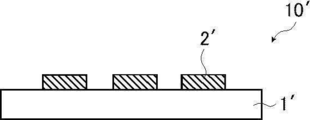
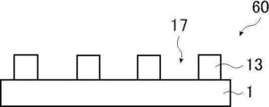
- FIG. 1 is a schematic view of the conductive substrate 10 formed by the first embodiment of the method X for manufacturing a conductive substrate.
- the conductive substrate 10 has a substrate 1 and a patterned conductive layer 2 arranged on the substrate 1.
- the thickness of the patterned conductive layer 2 is preferably 5.0 ⁇ m or less, more preferably 3.0 ⁇ m or less, in that the defective rate of the formed conductive substrate is lower.
- the lower limit is, for example, 0.1 ⁇ m or more, preferably 0.2 ⁇ m or more.
- Step X1A is a photosensitive transfer member having a temporary support and a photosensitive resin layer formed from a photosensitive resin composition containing an acid-degradable resin and a photoacid generator, which is arranged on the temporary support. Is a step of forming a photosensitive resin layer on a substrate using the above. Hereinafter, the procedure will be described after explaining the material used in the step X1A.
- the photosensitive resin composition contains an acid-decomposable resin and a photoacid generator.
- the photosensitive resin composition is preferably a chemically amplified photosensitive resin composition because it is more sensitive to exposure.
- a photoacid generator such as an onium salt and an oxime sulfonate compound described later is used, the acid generated in response to active radiation (hereinafter, also referred to as “active light”) is contained in the acid-degradable resin. It acts as a catalyst in the deprotection reaction of acid-degradable groups.
- the quantum yield exceeds 1, which is a large value such as the power of 10, which is high as a result of so-called chemical amplification. Sensitivity is obtained.
- a quinonediazide compound is used as a photoacid generator that is sensitive to active radiation, a carboxy group is generated by a sequential photochemical reaction, but the quantum yield is always 1 or less, and it does not correspond to the chemically amplified type.
- the photosensitive resin composition contains a polymer (acid-degradable resin) having a polar group (acid-degradable group) protected by a protecting group that is deprotected by the action of an acid.
- the acid-degradable resin is preferably a polymer containing a structural unit having an acid-degradable group (hereinafter, also referred to as “constituent unit A”) (hereinafter, also referred to as “polymer A”).
- consisttituent unit A hereinafter, also referred to as “polymer A”.
- the polymer A contains a structural unit having an acid-degradable group (constituent unit A).
- the acid-degradable group is deprotected by the action of an acid generated by exposure and converted into a polar group. Therefore, the photosensitive resin layer formed of the photosensitive resin composition has increased solubility in an alkaline developer upon exposure.
- the polymer A is preferably an addition polymerization type resin, and more preferably a polymer containing a structural unit derived from (meth) acrylic acid or (meth) acrylic acid ester.
- the polymer A contains a structural unit other than the structural unit derived from (meth) acrylic acid or (meth) acrylic acid ester (for example, a structural unit derived from styrene, a structural unit derived from a vinyl compound, etc.). You may be.
- the structural units that the polymer A may contain will be described.
- Polymer A contains a structural unit having an acid-degradable group.
- the acid-degradable group can be converted to a polar group by the action of an acid, as described above.
- the “polar group” refers to a proton dissociative group having a pKa of 12 or less.
- Examples of the polar group include known acid groups such as a carboxy group and a phenolic hydroxy group.
- the polar group is preferably a carboxy group or a phenolic hydroxy group.
- the protecting group is not particularly limited, and examples thereof include known protecting groups.
- the protecting groups include, for example, a protecting group capable of protecting a polar group in the form of acetal (for example, a tetrahydropyranyl group, a tetrahydrofuranyl group, and an ethoxyethyl group), and a protecting group capable of protecting a polar group in the form of an ester (for example, a protecting group capable of protecting a polar group in the form of an ester (eg, a tetrahydropyranyl group, a tetrahydrofuranyl group, and an ethoxyethyl group).
- a protecting group capable of protecting a polar group in the form of acetal for example, a tetrahydropyranyl group, a tetrahydrofuranyl group, and an ethoxyethyl group
- an ester for example, a protecting group capable of protecting a polar group in
- Examples of the acid-degradable group include acetal-based functional groups such as an ester group, a tetrahydropyranyl ester group, and a tetrahydrofuranyl ester group contained in a structural unit represented by the formula A3 described later, which are relatively easily decomposed by an acid. ), And a group that is relatively difficult to decompose with an acid (for example, a tertiary alkyl ester group such as a tert-butyl ester group and a tertiary alkyl carbonate group such as a tert-butyl carbonate group) can be used.
- a tertiary alkyl ester group such as a tert-butyl ester group
- a tertiary alkyl carbonate group such as a tert-butyl carbonate group
- the acid-degradable group is preferably a group in which a carboxy group or a phenolic hydroxy group is protected in the form of acetal.
- the structural unit A is selected from the group consisting of the structural unit represented by the formula A1, the structural unit represented by the formula A2, and the structural unit represented by the formula A3 in that the sensitivity and the resolution are more excellent. It is preferably a structural unit of more than one kind, and more preferably one or more kinds of structural units selected from the group consisting of the structural unit represented by the formula A1 and the structural unit represented by the formula A3. It is more preferable that the structural unit is one or more selected from the group consisting of the structural unit represented by the formula A1-2 and the structural unit represented by the formula A3-3 described later.
- the structural unit represented by the formula A1 and the structural unit represented by the formula A2 are structural units having an acid-degradable group protected by a protecting group in which the phenolic hydroxy group is deprotected by the action of an acid.
- the structural unit represented by the formula A3 is a structural unit having an acid-degradable group protected by a protecting group in which the carboxy group is deprotected by the action of an acid.
- R 11 and R 12 independently represent a hydrogen atom, an alkyl group, or an aryl group, respectively. However, at least one of R 11 and R 12 represents an alkyl group or an aryl group.
- R 13 represents an alkyl group or an aryl group.
- R 14 represents a hydrogen atom or a methyl group.
- X 1 represents a single bond or a divalent linking group.
- R 15 represents a substituent.
- n represents an integer from 0 to 4.
- one of the linked may form a cyclic ether (R 11 and R 12 form a cyclic ether linked together with R 13 together, R 11 And the other of R 12 may be a hydrogen atom, i.e. the other of R 11 and R 12 may not be an alkyl or aryl group).
- R 21 and R 22 independently represent a hydrogen atom, an alkyl group, or an aryl group, respectively. However, at least one of R 21 and R 22 represents an alkyl group or an aryl group.
- R 23 represents an alkyl group or an aryl group.
- R 24 is independently a hydroxy group, a halogen atom, an alkyl group, an alkoxy group, an alkenyl group, an aryl group, an aralkyl group, an alkoxycarbonyl group, a hydroxyalkyl group, an arylcarbonyl group, an aryloxycarbonyl group, or a cyclo.
- m represents an integer of 0 to 3.
- R 21 or R 22 and R 23 may be linked to each other to form a cyclic ether (when one of R 21 and R 22 is linked to R 23 to form a cyclic ether, R 21 and R
- the other of 22 may be a hydrogen atom, i.e. the other of R 21 and R 22 may not be an alkyl or aryl group).
- R 31 and R 32 each independently represent a hydrogen atom, an alkyl group, or an aryl group. However, at least one of R 31 and R 32 represents an alkyl group or an aryl group.
- R 33 represents an alkyl group or an aryl group.
- R 34 represents a hydrogen atom or a methyl group.
- X 0 represents a single bond or a divalent linking group.
- R 31 or R 32 and R 33 may be connected to each other to form a cyclic ether (when one of R 31 and R 32 is connected to R 33 to form a cyclic ether, R 31 may be formed.
- the other of R 32 may be a hydrogen atom, that is, the other of R 31 and R 32 may not be an alkyl or aryl group).
- the number of carbon atoms of the alkyl group represented by R 11 and R 12 is preferably 1 to 10.
- the aryl group represented by R 11 and R 12 a phenyl group is preferable.
- R 11 and R 12 are preferably a hydrogen atom or an alkyl group having 1 to 4 carbon atoms.
- examples of the alkyl group or aryl group represented by R 13 include those similar to the alkyl group and aryl group represented by R 11 and R 12.
- alkyl and aryl groups in R 11 , R 12 , and R 13 may further have substituents.
- R 11 or R 12 and R 13 are connected to each other to form a cyclic ether.
- the number of ring members of the cyclic ether is preferably 5 or 6, and more preferably 5.
- the alkylene group may be linear, branched, or cyclic, and may further have a substituent.
- the alkylene group preferably has 1 to 10 carbon atoms, and more preferably 1 to 4 carbon atoms.
- the RN represents an alkyl group or a hydrogen atom, and an alkyl group or a hydrogen atom having 1 to 4 carbon atoms is preferable, and a hydrogen atom is more preferable.
- the group represented by -OC (R 11 ) (R 12 ) -OR 13 specified in the formula and X 1 are specified in the formula in terms of steric hindrance of the acid-degradable group. It is preferable that they are bonded to each other at the para position on the benzene ring. That is, the structural unit represented by the formula A1 is preferably the structural unit represented by the following formula A1-1. Incidentally, R 11 in the formula A1-1, R 12, R 13, R 14, R 15, X 1, and n, respectively, R 11 in the formula A1, R 12, R 13, R 14, R 15, X It is synonymous with 1 and n.
- R 15 is preferably an alkyl group or a halogen atom.
- the alkyl group preferably has 1 to 10 carbon atoms, and more preferably 1 to 4 carbon atoms.
- n is preferably 0 or 1, more preferably 0.
- the R 14 in that the glass transition temperature of the polymer A (Tg) may be lower and a hydrogen atom is preferable. More specifically, the content of the structural unit in which R 14 is a hydrogen atom in the formula A1 is preferably 20% by mass or more with respect to the total content of the structural unit A contained in the polymer A. The content of the structural unit in which R 14 in the formula A1 is a hydrogen atom in the structural unit A is confirmed by the intensity ratio of the peak intensity calculated by a conventional method from 13 C-nuclear magnetic resonance spectrum (NMR) measurement. it can.
- NMR 13 C-nuclear magnetic resonance spectrum
- the structural unit represented by the following formula A1-2 is more preferable in that the deformation suppression of the pattern shape is more excellent.
- R B4 represents a hydrogen atom or a methyl group.
- R B5 to R B11 independently represent a hydrogen atom or an alkyl group having 1 to 4 carbon atoms.
- RB12 represents a substituent.
- n represents an integer from 0 to 4.
- R B4 is preferably a hydrogen atom.
- R B5 ⁇ R B11 is preferably a hydrogen atom.
- R B12 is preferably an alkyl group or a halogen atom.
- the alkyl group preferably has 1 to 10 carbon atoms, and more preferably 1 to 4 carbon atoms.
- 0 or 1 is preferable, and 0 is more preferable as n.
- R B4 in the structural unit of the following represents a hydrogen atom or a methyl group.
- the number of carbon atoms of the alkyl group represented by R 21 and R 22 is preferably 1 to 10.
- a phenyl group is preferable.
- examples of the alkyl group or aryl group represented by R 23 include those similar to the alkyl group and aryl group represented by R 21 and R 22.
- R 23 an alkyl group having 1 to 10 carbon atoms is preferable, and an alkyl group having 1 to 6 carbon atoms is more preferable.
- the alkyl and aryl groups in R 21 , R 22 , and R 23 may further have substituents.
- R 24 is preferably an alkyl group having 1 to 10 carbon atoms or an alkoxy group having 1 to 10 carbon atoms independently, and more preferably an alkyl group having 1 to 4 carbon atoms. preferable.
- R 24 may further have a substituent. Examples of the substituent include an alkyl group having 1 to 10 carbon atoms and an alkoxy group having 1 to 10 carbon atoms.
- the number of carbon atoms of the alkyl group represented by R 31 and R 32 is preferably 1 to 10.
- the aryl group represented by R 31 and R 32 a phenyl group is preferable.
- R 31 and R 32 are preferably a hydrogen atom or an alkyl group having 1 to 4 carbon atoms.
- R 33 an alkyl group having 1 to 10 carbon atoms is preferable, and an alkyl group having 1 to 6 carbon atoms is more preferable.
- the alkyl group and aryl group in R 31 to R 33 may further have a substituent.
- R 31 or R 32 and R 33 are connected to each other to form a cyclic ether.
- the number of ring members of the cyclic ether is preferably 5 or 6, and more preferably 5.
- a single bond or an arylene group is preferable, and a single bond is more preferable.
- the arylene group may further have a substituent.
- the glass transition temperature of the polymer A (Tg) may be lower and a hydrogen atom is preferable. More specifically, the content of the structural unit in which R 34 is a hydrogen atom in the formula A3 is 20% by mass or more with respect to the total content of the structural unit represented by the formula A3 contained in the polymer A. Is preferable.
- the content of the structural unit in which R 34 is a hydrogen atom in the structural unit represented by the formula A3 is the peak intensity calculated by a conventional method from the 13 C-nuclear magnetic resonance spectrum (NMR) measurement. It can be confirmed by the strength ratio of.
- the structural unit represented by the following formula A3-3 is more preferable in that the sensitivity at the time of pattern formation is further increased.
- R 34 represents a hydrogen atom or a methyl group.
- R 35 to R 41 independently represent a hydrogen atom or an alkyl group having 1 to 4 carbon atoms.
- R 34 is preferably a hydrogen atom.
- R 35 to R 41 are preferably hydrogen atoms.
- R 34 in the following constitutional unit represents a hydrogen atom or a methyl group.
- the structural unit A contained in the polymer A only one type may be used alone, or two or more types may be used in combination.
- the content of the structural unit A in the polymer A is preferably 20% by mass or more, more preferably 20 to 90% by mass, and 20 to 70% by mass with respect to the total mass of the polymer A. Is more preferable.
- the content of the structural unit A in the polymer A can be confirmed by the intensity ratio of the peak intensity calculated by a conventional method from 13 C-NMR measurement.
- the polymer A preferably contains a structural unit having a polar group (hereinafter, also referred to as “constituent unit B”).
- the polymer A contains the structural unit B, the sensitivity at the time of pattern formation is improved, and the solubility in an alkaline developer is improved in the developing step after pattern exposure.
- the polar group in the structural unit B is a proton dissociative group having a pKa of 12 or less.
- the upper limit of the pKa of the polar group is preferably 10 or less, more preferably 6 or less, in terms of further improving the sensitivity.
- the lower limit is preferably ⁇ 5 or higher.
- Examples of the polar group in the structural unit B include a carboxy group, a sulfonamide group, a phosphonic acid group, a sulfonic acid group, a phenolic hydroxy group, a sulfonylimide group and the like.
- a carboxy group or a phenolic hydroxy group is preferable.
- Examples of the method for introducing the structural unit B into the polymer A include a method of copolymerizing a monomer having a polar group and a method of copolymerizing a monomer having an acid anhydride structure to hydrolyze the acid anhydride.
- Examples of the monomer having a carboxy group as a polar group include acrylic acid, methacrylic acid, itaconic acid, crotonic acid, maleic acid, fumaric acid, 4-carboxystyrene and the like.
- Examples of the monomer having a phenolic hydroxy group as a polar group include p-hydroxystyrene and 4-hydroxyphenylmethacrylate.
- Examples of the monomer having an acid anhydride structure include maleic anhydride and the like.
- the structural unit B is preferably a structural unit derived from a styrene compound having a polar group, or a structural unit derived from a vinyl compound having a polar group, and a structural unit derived from a styrene compound having a phenolic hydroxy group.
- it is more preferably a structural unit derived from a vinyl compound having a carboxy group, further preferably a structural unit derived from a vinyl compound having a carboxy group, and a structural unit derived from (meth) acrylic acid. Is particularly preferable.
- structural unit B only one type may be used alone, or two or more types may be used in combination.
- the content of the structural unit B in the polymer A is preferably 0.1 to 20% by mass, more preferably 0.5 to 15% by mass, based on the total mass of the polymer A. It is more preferably 1 to 10% by mass.
- the content of the structural unit B in the polymer A can be confirmed by the intensity ratio of the peak intensity calculated by a conventional method from 13 C-NMR measurement.
- the polymer A may further contain other structural units (hereinafter, also referred to as “constituent unit C”) in addition to the above-mentioned structural unit A and structural unit B.
- Constituent unit C also referred to as “constituent unit C”
- Various characteristics of the polymer A can be adjusted by adjusting at least one of the type and the content of the structural unit C contained in the polymer A.
- the glass transition temperature (Tg) of the polymer A can be easily adjusted by appropriately using the structural unit C.
- Examples of the monomer forming the structural unit C include styrenes, (meth) acrylic acid alkyl esters, (meth) acrylic acid cyclic alkyl esters, (meth) acrylic acid aryl esters, unsaturated dicarboxylic acid diesters, and bicyclounsaturated compounds. , Maleimide compounds, unsaturated aromatic compounds, conjugated diene compounds, unsaturated monocarboxylic acids, unsaturated dicarboxylic acids, unsaturated dicarboxylic acid anhydrides, unsaturated compounds with an aliphatic cyclic skeleton, and other known unsaturated substances. Saturated compounds and the like can be mentioned.
- Examples of the structural unit C include styrene, tert-butoxystyrene, methylstyrene, ⁇ -methylstyrene, acetoxystyrene, methoxystyrene, and ethoxystyrene.
- Chlorostyrene methyl vinyl benzoate, ethyl vinyl benzoate, methyl (meth) acrylate, ethyl (meth) acrylate, n-propyl (meth) acrylate, isopropyl (meth) acrylate, 2- (meth) acrylate
- Examples thereof include structural units derived from hydroxyethyl, 2-hydroxypropyl (meth) acrylate, benzyl (meth) acrylate, isobornyl (meth) acrylate, acrylonitrile, and ethylene glycol monoacetate acetate mono (meth) acrylate.
- structural unit C a structural unit derived from the compound described in paragraphs 0021 to 0024 of JP2004-246623A can be mentioned.
- the structural unit C is preferably a structural unit having an aromatic ring or a structural unit having an aliphatic cyclic skeleton from the viewpoint of further improving the electrical characteristics.
- the monomer forming the above-mentioned structural unit include styrene, tert-butoxystyrene, methylstyrene, ⁇ -methylstyrene, dicyclopentanyl (meth) acrylate, cyclohexyl (meth) acrylate, isobornyl (meth) acrylate, and Benzyl (meth) acrylate and the like can be mentioned.
- the structural unit C is preferably a structural unit derived from cyclohexyl (meth) acrylate.
- the structural unit C is preferably a (meth) acrylic acid alkyl ester in that it has better adhesion, and has an alkyl group having 4 to 12 carbon atoms. More preferably, it is a (meth) acrylic acid alkyl ester. Specific examples thereof include methyl (meth) acrylate, ethyl (meth) acrylate, propyl (meth) acrylate, n-butyl (meth) acrylate, and 2-ethylhexyl (meth) acrylate.
- the polymer A includes, as the structural unit C, a structural unit having an ester of the polar group in the structural unit B, in terms of further improving the solubility in a developing solution and / or optimizing the physical properties. Is also preferable.
- the polymer A preferably contains a structural unit having a carboxy group as the structural unit B, and further preferably contains a structural unit C containing a carboxylic acid ester group.
- a structural unit derived from (meth) acrylic acid for example, a structural unit derived from (meth) acrylic acid.
- ⁇ contains B and a monomer-derived structural unit C selected from the group consisting of cyclohexyl (meth) acrylate, 2-ethylhexyl (meth) acrylate, and n-butyl (meth) acrylate.
- structural unit C only one type may be used alone, or two or more types may be used in combination.
- the upper limit of the content of the structural unit C in the polymer A is preferably 80% by mass or less, more preferably 75% by mass or less, and 60% by mass, based on the total mass of the polymer A. It is more preferably% or less, and particularly preferably 50% by mass or less.
- the lower limit of the content of the structural unit C in the polymer A may be 0% by mass, preferably 1% by mass or more, and 5% by mass or more, based on all the structural units constituting the polymer A. Is more preferable.
- the polymer A may be used alone or in combination of two or more.
- the content of the polymer A in the photosensitive resin composition is preferably 50 to 99.9% by mass, more preferably 70 to 98% by mass, based on the total solid content of the composition.
- the glass transition temperature (Tg) of the polymer A is preferably 90 ° C. or lower, more preferably 20 to 60 ° C. from the viewpoint of transferability. , 30 to 50 ° C. is particularly preferable.
- the glass transition temperature (Tg) of the polymer A As a method of adjusting the glass transition temperature (Tg) of the polymer A within the above numerical range, for example, examples thereof include a method of adjusting the type and mass fraction of each structural unit contained in the polymer A using the FOX formula as a guideline. By using the FOX formula, the glass transition temperature (Tg) of the polymer A is adjusted from the glass transition temperature (Tg) of the homopolymer of each structural unit contained in the polymer A and the mass fraction of each structural unit. it can. Further, the glass transition temperature (Tg) of the polymer A can be adjusted by adjusting the weight average molecular weight of the polymer A.
- the glass transition temperature of the homopolymer of the first structural unit is Tg1
- the mass fraction of the first structural unit contained in the copolymer is W1
- the glass transition temperature of the homopolymer of the second structural unit Is Tg2, and when the mass fraction of the second constituent unit contained in the copolymer in the copolymer is W2, Tg0 of the copolymer containing the first constituent unit and the second constituent unit is taken as Tg0.
- (Unit: K) is It can be estimated according to the following formula.
- the acid value of polymer A is preferably 0 to 200 mgKOH / g, more preferably 0 to 100 mgKOH / g.
- the acid value of the polymer represents the mass of potassium hydroxide required to neutralize the acidic component per 1 g of the polymer.
- the obtained solution is neutralized and titrated with a 0.1 M aqueous sodium hydroxide solution at 25 ° C.
- the acid value is calculated by the following formula with the inflection point of the titration pH curve as the titration end point.
- the weight average molecular weight of the polymer A is preferably 2,000 to 60,000, more preferably 3,000 to 50,000.
- the weight average molecular weight of the polymer A can be measured by GPC (gel permeation chromatography), and various commercially available devices can be used as the measuring device.
- GPC gel permeation chromatography
- HLC registered trademark
- -8220 GPC manufactured by Tosoh Corporation
- TSKgel registered trademark
- Super HZM-M 4.
- the calibration curve is "Standard sample TSK standard, polystyrene” manufactured by Tosoh Corporation: “F-40", “F-20”, “F-4", “F-1", "A-5000", “A”. It can be prepared using any of 7 samples of "-2500” and "A-1000".
- the ratio (dispersity) of the number average molecular weight of the polymer A to the weight average molecular weight is preferably 1.0 to 5.0, and more preferably 1.05 to 3.5.
- the method for producing polymer A is not particularly limited, but to give an example, a polymerizable monomer for forming the structural unit A and a polymerizable monomer for forming the structural unit B.
- a monomer and, if necessary, a polymerizable monomer for forming the structural unit C can be synthesized by polymerizing in an organic solvent with a polymerization initiator. Further, the polymer A can also be synthesized by a so-called polymer reaction.
- the photosensitive resin composition may further contain a polymer containing no structural unit having an acid-degradable group (hereinafter, also referred to as “other polymer”).
- Examples of other polymers include polyhydroxystyrene and the like.
- Examples of polyhydroxystyrene include SMA 1000P, SMA 2000P, SMA 3000P, SMA 1440F, SMA 17352P, SMA 2625P, and SMA 3840F (all manufactured by Sartmer), ARUFON UC-3000, ARUFON UC-3510, and ARUFON UC-. 3900, ARUFON UC-3910, ARUFON UC-3920, ARUFON UC-3080 (above, manufactured by Toa Synthetic Co., Ltd.), and Joncryl 690, Joncryl 678, Joncryl 67, and Joncryl 586 (above, BASF) Goods can be used.
- the content of the other polymers in the photosensitive resin composition is 50% by mass or less with respect to the total content of the polymer A and the other polymers. It is preferably 30% by mass or less, more preferably 20% by mass or less.
- the photosensitive resin composition contains a photoacid generator.
- the photoacid generator is a compound capable of generating an acid by being irradiated with radiation such as ultraviolet rays, far ultraviolet rays, X-rays, and charged particle beams.
- a compound that is sensitive to active light having a wavelength of 300 nm or more, preferably a wavelength of 300 to 450 nm and generates an acid is preferable.
- a compound having absorption at a wavelength of 365 nm is more preferable in that the spectral sensitivity is more excellent.
- a photoacid generator that is not directly sensitive to active light having a wavelength of 300 nm or more can be used as a sensitizer if it is a compound that is sensitive to active light having a wavelength of 300 nm or more and generates an acid when used in combination with a sensitizer. Can be preferably used in combination.
- the photoacid generator is preferably a photoacid generator that generates an acid having a pKa of 4 or less, more preferably a photoacid generator that generates an acid having a pKa of 3 or less, and a pKa of 2 or less.
- a photoacid generator that generates an acid is particularly preferable.
- the lower limit of the pKa of the acid generated from the photoacid generator is not particularly limited, and is preferably -10 or more, for example.
- the photoacid generator examples include an ionic photoacid generator and a nonionic photoacid generator. Further, the photoacid generator preferably contains one or more compounds selected from the group consisting of an onium salt compound and an oxime sulfonate compound, and more preferably contains an oxime sulfonate compound, because the photoacid generator is more excellent in sensitivity and resolution. preferable.
- Examples of the ionic photoacid generator include onium salt compounds such as diaryliodonium salts and triarylsulfonium salts, and quaternary ammonium salts.
- onium salt compounds are preferable, and diaryliodonium salts or triarylsulfonium salts are more preferable.
- the ionic photoacid generator described in paragraphs 0114 to 0133 of JP-A-2014-85643 can also be preferably used.
- nonionic photoacid generator examples include trichloromethyl-s-triazines, diazomethane compounds, imide sulfonate compounds, oxime sulfonate compounds and the like.
- an oxime sulfonate compound is particularly preferable in that sensitivity, resolution, and adhesion are improved.
- Specific examples of the trichloromethyl-s-triazines and the diazomethane derivative include the compounds described in paragraphs 0083 to 0088 of Japanese Patent Application Laid-Open No. 2011-22149.
- oxime sulfonate compound that is, the compound having an oxime sulfonate structure
- a compound having an oxime sulfonate structure represented by the following formula (B1) is preferable.
- R 21 represents an alkyl group or an aryl group
- * represents a binding site with another atom or another group.
- the compound having an oxime sulfonate structure represented by the formula (B1) may be substituted with any group, and the alkyl group at R 21 may be linear, branched chain, or cyclic. .. Acceptable substituents are described below.
- alkyl group represented by R 21 a linear or branched alkyl group having 1 to 10 carbon atoms is preferable.
- the alkyl group represented by R 21 has an aryl group having 6 to 11 carbon atoms, an alkoxy group having 1 to 10 carbon atoms, a cycloalkyl group (for example, a 7,7-dimethyl-2-oxonorbornyl group and the like). It may be substituted with a bridge-type alicyclic group, preferably a bicycloalkyl group or the like), or a halogen atom.
- aryl group in R 21 an aryl group having 6 to 18 carbon atoms is preferable, and a phenyl group or a naphthyl group is more preferable.
- the aryl group in R 21 may be substituted with one or more groups selected from the group consisting of alkyl groups having 1 to 4 carbon atoms, alkoxy groups, and halogen atoms.
- the compound having an oxime sulfonate structure represented by the formula (B1) is preferably the oxime sulfonate compound described in paragraphs 0078 to 0111 of JP-A-2014-85643.
- the photoacid generator may be used alone or in combination of two or more.
- the content of the photoacid generator in the photosensitive resin composition is preferably 0.1 to 10% by mass, preferably 0.2 to 10% by mass, based on the total mass of the composition, in that the sensitivity and resolution are more excellent. It is more preferably to 5% by mass.
- the photosensitive resin composition may contain a solvent.
- Examples of the solvent include ethylene glycol monoalkyl ethers, ethylene glycol dialkyl ethers, ethylene glycol monoalkyl ether acetates, propylene glycol monoalkyl ethers, propylene glycol dialkyl ethers, propylene glycol monoalkyl ether acetates, and diethylene glycol dialkyl.
- Examples thereof include ethers, diethylene glycol monoalkyl ether acetates, dipropylene glycol monoalkyl ethers, dipropylene glycol dialkyl ethers, dipropylene glycol monoalkyl ether acetates, esters, ketones, amides, lactones and the like. ..
- examples of the solvent include the solvents described in paragraphs 0174 to 0178 of JP-A-2011-22149, and the contents thereof are incorporated in the present disclosure.
- the photosensitive resin composition further comprises benzyl ethyl ether, dihexyl ether, ethylene glycol monophenyl ether acetate, diethylene glycol monomethyl ether, diethylene glycol monoethyl ether, isophorone, caproic acid, as required. It may contain solvents such as caprylic acid, 1-octanol, 1-nonal, benzyl alcohol, anisole, benzyl acetate, ethyl benzoate, diethyl oxalate, diethyl maleate, ethylene carbonate, and propylene carbonate.
- solvents such as caprylic acid, 1-octanol, 1-nonal, benzyl alcohol, anisole, benzyl acetate, ethyl benzoate, diethyl oxalate, diethyl maleate, ethylene carbonate, and propylene carbonate.
- the solvent is preferably a solvent having a boiling point of 130 ° C. or higher and lower than 160 ° C., a solvent having a boiling point of 160 ° C. or higher, or a mixture thereof.
- Examples of the solvent having a boiling point of 130 ° C. or higher and lower than 160 ° C. include propylene glycol monomethyl ether acetate (boiling point 146 ° C.), propylene glycol monoethyl ether acetate (boiling point 158 ° C.), propylene glycol methyl-n-butyl ether (boiling point 155 ° C.). And propylene glycol methyl-n-propyl ether (boiling point 131 ° C.) and the like.
- Examples of the solvent having a boiling point of 160 ° C. or higher include ethyl 3-ethoxypropionate (boiling point 170 ° C.), diethylene glycol methyl ethyl ether (boiling point 176 ° C.), propylene glycol monomethyl ether propionate (boiling point 160 ° C.), and dipropylene glycol methyl.
- Ether acetate (boiling point 213 ° C), 3-methoxybutyl ether acetate (boiling point 171 ° C), diethylene glycol diethyl ether (boiling point 189 ° C), diethylene glycol dimethyl ether (boiling point 162 ° C), propylene glycol diacetate (boiling point 190 ° C), diethylene glycol monoethyl ether Examples thereof include acetate (boiling point 220 ° C.), dipropylene glycol dimethyl ether (boiling point 175 ° C.), and 1,3-butylene glycol diacetate (boiling point 232 ° C.).
- solvent examples include esters, ethers, ketones and the like.
- esters examples include ethyl acetate, propyl acetate, isobutyl acetate, sec-butyl acetate, t-butyl acetate, isopropyl acetate, n-butyl acetate and the like.
- ethers include diisopropyl ether, 1,4-dioxane, 1,2-dimethoxyethane, 1,3-dioxolane, propylene glycol dimethyl ether, propylene glycol monoethyl ether and the like.
- ketones examples include methyl n-butyl ketone, methyl ethyl ketone, methyl isobutyl ketone, diethyl ketone, methyl n-propyl ketone, methyl isopropyl ketone and the like.
- solvent toluene, acetonitrile, isopropanol, 2-butanol, isobutyl alcohol and the like may be used.
- the solvent may be used alone or in combination of two or more.
- the content of the solvent in the photosensitive resin composition is preferably 50 to 1,900 parts by mass, more preferably 100 to 900 parts by mass, based on 100 parts by mass of the total solid content of the composition. ..
- the photosensitive resin composition may further contain other additives, if necessary, in addition to the polymer A and the photoacid generator.
- the photosensitive resin composition preferably contains a basic compound.
- the basic compound include aliphatic amines, aromatic amines, heterocyclic amines, quaternary ammonium hydroxides, and quaternary ammonium salts of carboxylic acids. Specific examples of these include the compounds described in paragraphs 0204 to 0207 of JP-A-2011-22149, the contents of which are incorporated in the present disclosure.
- Examples of the aliphatic amine include trimethylamine, diethylamine, triethylamine, di-n-propylamine, tri-n-propylamine, di-n-pentylamine, tri-n-pentylamine, diethanolamine, triethanolamine and dicyclohexylamine. , And dicyclohexylmethylamine and the like.
- aromatic amines examples include aniline, benzylamine, N, N-dimethylaniline, diphenylamine and the like.
- heterocyclic amine examples include pyridine, 2-methylpyridine, 4-methylpyridine, 2-ethylpyridine, 4-ethylpyridine, 2-phenylpyridine, 4-phenylpyridine, N-methyl-4-phenylpyridine, and the like.
- Examples of the quaternary ammonium hydroxide include tetramethylammonium hydroxide, tetraethylammonium hydroxide, tetra-n-butylammonium hydroxide, and tetra-n-hexylammonium hydroxide.
- Examples of the quaternary ammonium salt of the carboxylic acid include tetramethylammonium acetate, tetramethylammonium benzoate, tetra-n-butylammonium acetate, and tetra-n-butylammonium benzoate.
- the basic compound may be used alone or in combination of two or more.
- the content of the basic compound in the photosensitive resin composition is preferably 0.001 to 5% by mass, more preferably 0.005 to 3% by mass, based on the total mass of the composition. ..
- the photosensitive resin composition preferably contains a liquid repellent from the viewpoint of further improving the uniformity of thickness and further reducing the defective rate of the conductive substrate to be formed.
- a liquid repellent a compound containing at least one of a fluorine atom and a silicon atom is preferable, a fluorine atom-containing compound is more preferable, a fluorine atom-containing surfactant is further preferable, and a fluorine atom-containing nonionic surfactant is particularly preferable.
- a liquid repellent having a polymerizable group hereinafter, also referred to as “polymerizable group-containing liquid repellent” can be used as the polymerizable group. Examples of the polymerizable group include an epoxy group and an ethylenically unsaturated group.
- a compound represented by the general formula (1) of JP2013-209636A can also be used.
- a fluorine atom-containing nonionic surfactant is preferable.
- a preferable example of the fluorine atom-containing nonionic surfactant is measured by gel permeation chromatography containing the structural unit SA and the structural unit SB represented by the following formula I-1 and using tetrahydrofuran (THF) as a solvent.
- THF tetrahydrofuran
- examples thereof include copolymers having a polystyrene-equivalent weight average molecular weight (Mw) of 1,000 to 10,000.
- R 401 and R 403 independently represent a hydrogen atom or a methyl group, respectively.
- R 402 represents a linear alkylene group having 1 to 4 carbon atoms.
- R 404 represents a hydrogen atom or an alkyl group having 1 to 4 carbon atoms.
- L represents an alkylene group having 3 to 6 carbon atoms.
- p and q are mass percentages representing the polymerization ratio.
- p represents a numerical value of 10 to 80% by mass
- q represents a numerical value of 20 to 90% by mass.
- r represents an integer from 1 to 18.
- s represents an integer from 1 to 10. * Represents a binding site with another structure.
- L is preferably a branched alkylene group represented by the following formula I-2.
- R405 in the formula I-2 represents an alkyl group having 1 to 4 carbon atoms, and an alkyl group having 1 to 3 carbon atoms is preferable in terms of compatibility and wettability to the surface to be coated, and the alkyl group has 2 or 3 carbon atoms. Alkyl groups are more preferred.
- the weight average molecular weight (Mw) of the copolymer containing the structural unit SA and the structural unit SB represented by the formula I-1 is preferably 1,500 to 5,000.
- liquid repellent other than the above-mentioned copolymer
- fluorine atom-containing compound examples include perfluoroalkyl sulfonic acid, perfluoroalkylcarboxylic acid, perfluoroalkylalkylene oxide adduct, perfluoroalkyltrialkylammonium salt, oligomer containing perfluoroalkyl group and hydrophilic group, and perfluoro.
- Examples thereof include oligomers containing alkyl and lipophilic groups, oligomers containing perfluoroalkyl groups and hydrophilic groups and lipophilic groups, urethanes containing perfluoroalkyl and hydrophilic groups, perfluoroalkyl esters, perfluoroalkyl phosphate esters and the like. ..
- fluorine atom-containing compounds include "DEFENSAMCF-300”, “DEFENSAMCF-310”, “DEFENSAMCF-312”, “DEFENSAMCF-323”, and "Megafuck RS-72-K” (all manufactured by DIC).
- Fluorine atom-containing surfactant can also be used.
- Florard FC430, FC431, and FC171 all manufactured by Sumitomo 3M Ltd.
- Surflon S-382, SC-101, SC-103, SC-104, SC-105, SC-1068, SC-381, SC-383, S-393, and KH-40 aboveve, manufactured by AGC Inc.
- PolyFox PF636, PF656, PF6320, PF6520, and PF7002 aboveve, manufactured by OMNOVA
- Futergent 710FL, 710FM can also be used.
- 610FM, 601AD, 601ADH2, 602A, 215M, 245F, 251, 212M, 250, 209F, 222F, 208G, 710LA, 710FS, 730LM, 650AC, 681, and 683 are also used. it can.
- a fluorine atom-containing nonionic surfactant such as Futagent 250 manufactured by Neos Co., Ltd. and Futagent 251 can also be used.
- the fluorine atom-containing compound the surfactants described in paragraphs 0017 of Japanese Patent No. 4502784 and paragraphs 0060 to 0071 of Japanese Patent Application Laid-Open No. 2009-237362 can also be used.
- fluorine-based surfactant from the viewpoint of improving environmental suitability, compounds having a linear perfluoroalkyl group having 7 or more carbon atoms, such as perfluorooctanoic acid (PFOA) and perfluorooctanesulfonic acid (PFOS), are used. It is preferably a surfactant derived from an alternative material.
- PFOA perfluorooctanoic acid
- PFOS perfluorooctanesulfonic acid
- silicon atom-containing compounds examples include silicone-based surfactants such as the SILFOAM® series (for example, SD100TS, SD670, SD850, SD860, SD882) manufactured by Wacker Chemie.
- SILFOAM® series for example, SD100TS, SD670, SD850, SD860, SD882 manufactured by Wacker Chemie.
- the liquid repellent may be used alone or in combination of two or more.
- the lower limit of the content of fluorine atoms in the liquid repellent is preferably 1% by mass or more, more preferably 5% by mass or more.
- the upper limit value is preferably 50% by mass or less, more preferably 25% by mass or less.
- the content of the liquid repellent in the photosensitive resin composition is, for example, 0.01 to 10% by mass, preferably 0.05 to 5% by mass, based on the total solid content of the composition.
- the photosensitive resin composition preferably contains a surfactant from the viewpoint of further improving the uniformity of thickness.
- the surfactant referred to here does not include the above-mentioned surfactant-based liquid repellent.
- any of anionic surfactant, cationic surfactant, nonionic (nonionic) surfactant, and amphoteric surfactant can be used. Of these, nonionic surfactants are preferable.
- nonionic surfactants include polyoxyethylene higher alkyl ethers, polyoxyethylene higher alkyl phenyl ethers, and polyoxyethylene glycol higher fatty acid diesters. Specific examples of the nonionic surfactant include the nonionic surfactant described in paragraph 0120 of International Publication No. 2018/179640.
- the surfactant may be used alone or in combination of two or more.
- the content of the surfactant in the photosensitive resin composition is preferably 10% by mass or less, more preferably 0.001 to 10% by mass, and 0. It is more preferably 01 to 3% by mass.
- the photosensitive resin composition may contain a plasticizer for the purpose of improving plasticity.
- the plasticizer is not particularly limited, and a known plasticizer can be applied. Examples of the plasticizer include the plasticizers described in paragraphs 097 to 0103 of International Publication No. 2018/179640.
- the photosensitive resin composition may contain a sensitizer.
- the sensitizer is not particularly limited, and a known sensitizer can be applied. Examples of the sensitizer include the sensitizers described in paragraphs 0104 to 0107 of International Publication No. 2018/179640.
- the photosensitive resin composition may contain a heterocyclic compound.
- the heterocyclic compound is not particularly limited, and known heterocyclic compounds can be applied. Examples of the heterocyclic compound include the heterocyclic compounds described in paragraphs 0111 to 0118 of International Publication No. 2018/179640.
- the photosensitive resin composition may contain an alkoxysilane compound.
- the alkoxysilane compound is not particularly limited, and a known alkoxysilane compound can be applied. Examples of the alkoxysilane compound include the alkoxysilane compound described in paragraph 0119 of International Publication No. 2018/179640.
- Photosensitive resin compositions include metal oxide particles, antioxidants, dispersants, acid growth agents, development accelerators, conductive fibers, colorants, thermal radical polymerization initiators, thermal acid generators, and ultraviolet rays. It may further contain known additives such as absorbents, thickeners, cross-linking agents, and organic or inorganic anti-precipitation agents. Preferred embodiments of the other components are described in paragraphs 0165 to 0184 of JP2014-85643, respectively, and the contents of this publication are incorporated in the present specification.
- Method for preparing composition examples include a method in which the above components and a solvent are mixed at an arbitrary ratio and dissolved by stirring. Further, a photosensitive resin composition can be prepared by dissolving each of the above components in a solvent in advance to prepare a solution, and then mixing the obtained solutions in a predetermined ratio. The prepared photosensitive resin composition may be used after being filtered using a filter having a pore size of 0.2 ⁇ m or the like.
- the photosensitive transfer member has a temporary support and a photosensitive resin layer formed from the above-mentioned photosensitive resin composition arranged on the temporary support. Further, the photosensitive transfer member may have a protective film on the surface of the photosensitive resin layer opposite to the temporary support.
- Examples of the temporary support include a glass base material and a resin film.
- the temporary support may have a single-layer structure consisting of only one layer, or may have a multi-layer structure including two or more layers.
- the thickness of the temporary support is not particularly limited, and is, for example, 6 to 150 ⁇ m, preferably 12 to 50 ⁇ m.
- the photosensitive transfer member has a photosensitive resin layer formed from the above-mentioned photosensitive resin composition on a temporary support.
- the lower limit of the thickness of the photosensitive resin layer is preferably 1.0 ⁇ m or more from the viewpoint of transferability and resolvability.
- the upper limit value is, for example, 30.0 ⁇ m or less, preferably 15.0 ⁇ m or less, more preferably 10.0 ⁇ m or less, and further preferably 5.0 ⁇ m or less.
- Examples of the method for forming the photosensitive resin layer include a method in which a photosensitive resin composition is applied onto a temporary support to form a coating film, and then the coating film is dried.
- Examples of the coating method include known methods such as slit coating, spin coating, curtain coating, and inkjet coating.
- the drying temperature is not particularly limited, and is, for example, 80 to 150 ° C.
- the drying time is not particularly limited, and is, for example, 3 to 60 minutes.
- another layer such as an intermediate layer may be provided on the temporary support. When another layer such as an intermediate layer is arranged on the temporary support, a photosensitive resin layer is formed on the other layer. Examples of other layers include the layers described in paragraphs 0131 to 0134 of International Publication No. 2018/179640.
- the substrate is not particularly limited, but a glass substrate or a resin substrate is preferable, and a resin substrate is more preferable.
- the resin constituting the resin substrate include polycarbonate (PC), acrylonitrile-butadiene-styrene copolymer (ABS), acrylonitrile-styrene copolymer (AS), polypropylene (PP), polyethylene (PE), and polyamide ( PA), polyacetal (POM), polybutylene terephthalate (PBT), polyethylene terephthalate (PET), polyphenylene sulfide (PPS), polyetheretherketone (PEEK), polystyrene (PS), polymethylmethacrylate (PMMA), polyphenylene ether ( Examples thereof include resins such as PPE), polysulfone (PSF), polyethersulfone (PES), polyamideimide (PAI), polyetherimide (PEI), polyimide (PI), and polyvinyl chloride (PVC).
- PC polycarbon
- the surface of the substrate may be subjected to surface treatment such as hydrophilic treatment for the purpose of improving the adhesion to the conductive layer.
- the substrate has a visible region of 400 to 700 nm in that it facilitates exposure of the photosensitive resin layer from the surface of the substrate opposite to the side having the photosensitive resin layer (back surface of the substrate) via the substrate in step X5.
- the light transmittance of the above is preferably 50% or more, and more preferably the light transmittance at 400 to 450 nm is more than 10%.
- the thickness of the substrate is preferably 10 to 200 ⁇ m, more preferably 20 to 150 ⁇ m, and even more preferably 30 to 100 ⁇ m.
- step X1A the substrate and the photosensitive transfer member are bonded to each other by bringing the surface of the photosensitive resin layer on the side opposite to the temporary support side into contact with the substrate.
- the protective film is provided on the surface of the photosensitive resin layer opposite to the temporary support side, the substrate and the photosensitive transfer member are bonded together after removing the protective film from the photosensitive transfer member.
- a known laminator such as a laminator, a vacuum laminator, or an auto-cut laminator capable of further increasing productivity can be used for bonding the substrate and the photosensitive transfer member.
- a laminator such as a laminator, a vacuum laminator, or an auto-cut laminator capable of further increasing productivity
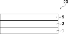
- the laminated body 20 shown in FIG. 2 can be obtained.
- the laminate 20 has a substrate 1, a photosensitive resin layer 3 and a temporary support 5 on the substrate 1.
- the step X2 is a step of exposing the photosensitive resin layer 3 of the laminate 20 obtained through the step X1 in a pattern.
- FIG. 3 schematically shows an example of the exposure process.
- the mask 6 having the opening 6a is arranged so as to be in close contact with the temporary support 5, and the photosensitive resin layer 3 of the laminated body 20 is exposed in a pattern through the temporary support 5.
- step X2 the acid-degradable resin in the exposed portion (position corresponding to the opening 6a) of the photosensitive resin layer 3 is deprotected by the action of the acid and dissolved in the alkaline developer. Increases sex.
- step X2 the exposed portion of the photosensitive resin layer 3 is removed in the subsequent developing step of step X3.
- the position and size of the opening of the mask are not particularly limited.
- the opening is opened from the viewpoint of improving the display quality of the display device and minimizing the area occupied by the take-out wiring.
- the shape is a fine line, and the width thereof is preferably 100 ⁇ m or less, more preferably 70 ⁇ m or less.
- any light source that irradiates the photosensitive resin layer with light in a wavelength range that can be exposed can be appropriately selected.
- Specific examples thereof include an ultra-high pressure mercury lamp, a high pressure mercury lamp, a metal halide lamp, and an LED (Light Emitting Diode).
- an ultra-high pressure mercury lamp for example, 365 nm, 405 nm, etc.
- a high pressure mercury lamp for example, 365 nm, 405 nm, etc.
- LED Light Emitting Diode
- the exposure amount is preferably 5 ⁇ 1000mJ / cm 2, more preferably 70 ⁇ 1000mJ / cm 2, more preferably 70 ⁇ 500mJ / cm 2.
- the exposure treatment may be performed after the temporary support 5 is peeled off from the photosensitive resin layer 3.
- the pattern exposure may be an exposure through a mask or a direct exposure using a laser or the like.
- Step X3 is a step of developing the photosensitive resin layer exposed in the pattern obtained in step X2 with an alkaline developer to form an opening penetrating the photosensitive resin layer.
- the temporary support 5 is peeled off from the laminated body 20.
- the laminate 30 obtained through the development process of step X3 has a substrate 1 and a photosensitive resin layer 3A arranged on the substrate 1 and having an opening 7 penetrating through the layer. Have. That is, the photosensitive resin layer 3A has an opening 7 in which the substrate 1 is exposed. The position of the opening 7 penetrating the photosensitive resin layer 3 coincides with the position of the opening (opening 6a in FIG.
- step X4 which will be described later, the conductive composition is supplied to the opening 7.
- the alkaline aqueous solution-based developer may further contain a water-soluble organic solvent, a surfactant, and the like.
- the alkaline aqueous solution-based developer for example, the developer described in paragraph 0194 of International Publication No. 2015/093271 is preferable.
- the development method is not particularly limited, and any of paddle development, shower development, spin development, dip development, etc. may be used.
- shower development will be described.
- the liquid temperature of the alkaline developer is preferably 20 to 40 ° C.
- Step X3 may further include a post-baking step of heat-treating the developed photosensitive resin layer.
- Post-baking is preferably carried out in an environment of 8.1 to 121.6 kPa, and more preferably carried out in an environment of 50.66 kPa or more. On the other hand, it is more preferably carried out in an environment of 111.46 kPa or less, and further preferably carried out in an environment of 101.3 kPa or less.
- the post-baking temperature is preferably 80 to 250 ° C, more preferably 110 to 170 ° C, and even more preferably 130 to 150 ° C.
- the post-baking time is preferably 1 to 30 minutes, more preferably 2 to 10 minutes, still more preferably 2 to 4 minutes. Post-baking may be performed in an air environment or a nitrogen substitution environment.
- Step X4 is a step of supplying the conductive composition to the opening 7 of the photosensitive resin layer 3A of the laminate 30 shown in FIG.
- FIG. 5 shows the laminated body 40 obtained through the step X4.
- the laminate 40 has a conductive composition layer 8A formed from the conductive composition in the opening 7 of the photosensitive resin layer 3A.
- the conductive composition is in a region other than the opening 7 (for example, the photosensitive resin layer 3A). It may adhere to the upper surface of the). Therefore, as a method of supplying the conductive composition, a method of applying the conductive composition to the entire surface of the photosensitive resin layer 3A may be used.
- the contact angle of the surface of the photosensitive resin layer 3A with respect to the conductive composition is preferably larger than the contact angle of the surface of the substrate 1 with respect to the conductive composition. That is, it is preferable that the conductive composition exhibits better wettability with respect to the surface of the substrate 1 than with respect to the surface of the photosensitive resin layer 3A.
- the contact angle of the surface of the photosensitive resin layer 3A with respect to the conductive composition is smaller than the contact angle of the surface of the substrate 1 with respect to the conductive composition, as shown in FIG.
- the opening 7 of the photosensitive resin layer 3A The conductive composition supplied to the above may easily crawl up the side surface of the photosensitive resin layer 3A and exude to the upper surface of the photosensitive resin layer 3A (see the conductive composition layer 8B in FIG. 6). As a result, defects such as short circuits tend to occur easily in the conductive layer 2 of the conductive substrate to be formed. Therefore, as described above, the contact angle of the surface of the photosensitive resin layer 3A with respect to the conductive composition is preferably larger than the contact angle of the surface of the substrate 1 with respect to the conductive composition.
- the surface of the photosensitive resin layer 3A preferably has a liquid-repellent property (repellent property) with respect to the conductive composition, and the surface of the substrate 1 is liquid-friendly to the conductive composition. It is preferable to have it.
- the liquid repellency and liquid friendship of the conductive composition can be evaluated by the following methods. A droplet of the conductive composition is deposited on the evaluation target, and the evaluation is performed based on the behavior of the droplet. When the surface area of the droplet decreases with respect to the amount of the droplet at the time of landing, the evaluation object has liquid repellency. On the other hand, when the surface area of the droplet increases with respect to the amount of the droplet at the time of drip, the evaluation object has positivity.
- the contact angle of the conductive composition with respect to the surface of the photosensitive resin layer 3A is preferably 30 ° or more, and the conductive composition with respect to the surface of the substrate 1 can be further reduced from the defect rate of the conductive substrate to be formed.
- the contact angle of is preferably less than 30 °.
- step X4 the procedure will be described after explaining the materials used in step X4.
- the conductive composition includes a conductive material.
- the conductive material is intended to include both a material that exhibits conductivity by itself and a material that can form a conductive layer after being sintered.
- the conductive material is a conductive material that exhibits conductivity by itself and can form a conductive layer having a sheet resistivity of less than 10 ⁇ / ⁇ at 23 ° C., or a sheet at 23 ° C. after being sintered.
- a conductive material capable of forming a conductive layer having a resistivity of less than 10 ⁇ / ⁇ is preferable.
- the conductive composition is not particularly limited, but for example, a composition in which a conductive material is dissolved or dispersed in a solvent, or a composition containing a conductive material and a binder polymer is preferable, and the conductive material is dispersed in a solvent.
- a composition hereinafter, also referred to as “composition C1”) or a composition containing a conductive material and a binder polymer (hereinafter, also referred to as “composition C2”) is more preferable, and the conductive material is dispersed in a solvent.
- composition C1 a composition containing a conductive material and a binder polymer
- composition C1 a composition containing a conductive material and a binder polymer
- the prepared composition is more preferable.
- As the conductive composition known conductive pastes and conductive inks, and plating-forming inks described later can also be used.
- the conductive material is not particularly limited, and examples thereof include those shown below, and (a) is preferable.
- Metal oxide particles (c) Conductive organic materials such as conductive polymer particles, and superconductivity Elementary particles (d) Organometallic compounds (e) Other conductive materials other than the above-mentioned (a) to (e)
- metal unit and alloy a metal unit selected from the group consisting of gold, silver, copper, nickel, aluminum, gold, platinum, and palladium, or an alloy composed of two or more of these metals is preferable, and the resistance value, Gold, silver, copper, or alloys thereof are more preferable from the viewpoint of cost, sintering temperature, and the like, and silver is preferable from the viewpoint of sintering temperature and oxidation suppression.
- metal single body or alloy in the shape of particles, clusters, crystals, tubes, fibers, wires, rods, films and the like described above, gold nanoparticles, silver nanoparticles, or copper nanoparticles are preferable, and silver is preferable. Nanoparticles are more preferred.
- the "metal oxide” is a compound that does not substantially contain an unoxidized metal. Specifically, a peak derived from an oxidized metal is detected in a crystal analysis by X-ray diffraction, and the metal. Refers to a compound in which no peak of origin is detected. It is not particularly limited that the unoxidized metal is not substantially contained, but it means that the content of the unoxidized metal is 1% by mass or less with respect to the metal oxide particles.
- the metal oxide in the metal oxide particles include oxides such as copper, silver, nickel, gold, platinum, palladium, indium, and tin.
- the metal oxide species may be one kind or a mixture of two or more kinds.
- an oxide of copper, silver, nickel, or tin is preferable, an oxide of copper or silver is more preferable, and an oxide of copper is further preferable.
- an oxide of copper copper (I) oxide or copper (II) oxide is preferable, and copper (II) oxide is more preferable because it can be obtained at low cost.
- the upper limit of the average particle size of the metal oxide particles is preferably less than 1 ⁇ m, more preferably less than 200 nm. The lower limit is preferably 1 nm or more.
- the average particle size of the metal oxide particles refers to the number average value of the particle size of the primary particles of 100 metal oxide particles randomly selected by observation with a scanning electron microscope (SEM).
- Conductive organic materials such as conductive polymers and superconductors
- conductive organic materials and superconductors include polyaniline, polythiophene, polyphenylene vinylene and the like.
- examples of the conductive organic material include PEDOT (polyethylene dioxythiophene) (PEDOT / PSS) doped with PPS (polystyrene sulfonic acid).
- Organometallic compound refers to a compound in which a metal is precipitated by decomposition by heating.
- organometallic compound examples include chlorotriethylphosphine gold, chlorotrimethylphosphine gold, chlorotriphenylphosphine gold, silver 2,4-pentandionato complex, trimethylphosphine (hexafluoroacetylacetonate) silver complex, and copper hexafluoropentaneo. Examples thereof include a natocyclooctadiene complex.
- Examples of the conductive material other than the above-mentioned (a) to (e) include a resist material, an acrylic resin as a linear insulating material, and a silane compound which becomes silicon by heating. These may be dispersed as particles in a solvent or may be dissolved and exist. Examples of the silane compound that becomes silicon by heating include trisilane, pentasilane, cyclotrisilane, and 1,1′-biscyclobutasilane.
- the conductive composition preferably contains a solvent and the main component thereof is water in that the defect rate of the conductive substrate to be formed is further reduced.
- the "main component” refers to the component having the largest amount (mass ratio) of the solvents contained in the conductive composition.
- the content of water is preferably more than 50% by mass, more preferably 55% by mass or more, based on the total mass of the solvent contained in the conductive composition. It is more preferably 60% by mass or more, particularly preferably 80% by mass or more, and most preferably 90% by mass or more.
- the upper limit of the water content is, for example, 100% by mass or less with respect to the total mass of the solvent contained in the composition C1.
- composition C1 preferably contains a conductive material, a solvent, and a dispersant.
- the composition C1 may further contain other components such as a polymerizable compound having an ethylene unsaturated group and a polymerization initiator.
- the conductive material contained in the composition C1 include the conductive materials described above.
- the composition C1 preferably has a viscosity of 1 to 20 mPa ⁇ s.
- the composition C1 is preferably a colloidal liquid in which a conductive material is dispersed in a dispersion medium.
- conductive particles are preferable, and silver nanoparticles are more preferable.
- the average particle size of the conductive particles is preferably 0.1 to 50 nm, more preferably 1 to 20 nm, from the viewpoint of stability and fusion temperature.
- the average particle size of the conductive particles refers to the number average value of the particle sizes of the primary particles of 100 conductive particles randomly selected.
- the content of the conductive material in the composition C1 is that the dispersion stability and the metal film forming property in the step of sintering the conductive composition layer in the step X7 (step Y6) described later are more excellent. , 10 to 95% by mass, more preferably 30 to 80% by mass, based on the total mass of the composition.
- the composition C1 preferably contains silver colloidal particles in which silver nanoparticles form a colloidal state, in that the conductive layer to be formed is less likely to be oxidized and the volume resistance value is less likely to decrease.
- the form of the silver colloidal particles is not particularly limited, and for example, a form in which a dispersant is attached to the surface of silver nanoparticles, a form in which silver nanoparticles are used as a core and the surface thereof is coated with a dispersant, and a form in which the surface is coated with a dispersant, and Examples thereof include a form in which silver particles and a dispersant are uniformly mixed, and among them, a form in which silver nanoparticles are used as a core and the surface thereof is coated with a dispersant, or silver particles and a dispersant. Is preferably a form in which is uniformly mixed.
- the silver colloidal particles having each of the above-mentioned forms can be appropriately prepared by a known method.
- the average particle size of the silver colloidal particles is preferably 1 to 400 nm because the dispersibility in the composition with time is more excellent and / or the resistance value of the conductive layer to be formed is further reduced. 1 to 70 nm is more preferable.
- the average particle size of the silver colloidal particles can be measured as a median diameter (D50) with the particle size as the volume standard by using the dynamic light scattering method (Doppler scattered light analysis).
- the composition C1 contains silver nanoparticles
- the composition C1 has a submicron size silver having a larger average particle size (for example, an average particle size of 1 ⁇ m or less) than the silver nanoparticles in addition to the silver nanoparticles. It may contain submicron particles.
- the silver nanoparticles have a melting point drop around the silver submicron particles, so that a good conductive path can be easily obtained.
- the composition C1 contains silver nanoparticles
- the composition C1 contains metal particles other than silver (hereinafter, “other metal particles”) in addition to the silver nanoparticles in that migration of the conductive layer can be suppressed.
- other metal particles metal particles other than silver
- a mixed colloidal solution of silver nanoparticles and other metal particles is more preferable.
- the metal other than silver a metal having an ionization series noble than hydrogen is preferable.
- gold, copper, platinum, palladium, rhodium, iridium, osmium, ruthenium, or renium is preferable, and gold, copper, platinum, or palladium is more preferable.
- composition C1 is a mixed colloidal liquid
- silver and other metals may form alloy colloidal particles, or may form colloidal particles having a structure such as a core-shell structure and a multilayer structure.
- the metal particles other than silver may be nano-sized particles or submicron-sized particles.
- Examples of the solvent contained in the composition C1 include water and an organic solvent, and water is preferable.
- the organic solvent is not particularly limited, and for example, hydrocarbons such as toluene, dodecane, tetradecane, cyclododecene, n-heptane, and n-undecane: saturated aliphatic monohydric alcohols such as ethanol, isopropyl alcohol, and butanol: Alkanediols such as propanediol, butanediol, and pentanediol: alkylene glycols such as ethylene glycol ,: diethylene glycol monoisobutyl ether, ethylene glycol monobutyl ether, ethylene glycol monoisobutyl ether, ethylene glycol isopropyl ether, ethylene glycol monomethyl ether, And glycol monoethers such as diethylene glycol monobutyl ether: glycerin and the like can be mentioned.
- the composition C1 preferably contains a solvent and the main component thereof is water in that the defect rate of the conductive substrate to be formed is further reduced.
- the "main component” refers to the component having the largest amount (mass ratio) of the solvents contained in the composition C1.
- the content of water is preferably more than 50% by mass, more preferably 55% by mass or more, and more preferably 60% by mass, based on the total mass of the solvent contained in the composition C1. % Or more is more preferable, 80% by mass or more is particularly preferable, and 90% by mass or more is most preferable.
- the upper limit of the water content is, for example, 100% by mass or less with respect to the total mass of the solvent contained in the composition C1.
- the content of the solvent is preferably 2 to 98% by mass, preferably 25 to 80% by mass, based on the total mass of the composition, in that the dispersibility stability of the conductive material is more excellent. It is more preferably by mass, more preferably 50 to 80% by mass, and particularly preferably 55 to 80% by mass.
- composition C1 contains water, as a dispersion medium other than water, from the group consisting of diethylene glycol monoisobutyl ether, ethylene glycol monobutyl ether, ethylene glycol monoisobutyl ether, ethylene glycol isopropyl ether, ethylene glycol monomethyl ether, and diethylene glycol monobutyl ether. It is also preferable to use one or more selected solvents in combination. In addition to this, it is also preferable to further use one or more solvents selected from the group consisting of butanol, propanediol, butanediol, pentanediol, ethylene glycol, and glycerin.
- the composition C1 may contain a dispersant as described above.
- the dispersant has a carboxy group and a hydroxyl group in that the dispersion stability of the conductive particles (particularly silver colloidal particles) in the composition is more excellent, and the number of carboxy groups contained in the molecule ⁇ the molecule. Hydroxylic acid or a salt thereof, which is the number of hydroxyl groups contained therein, is preferable.
- Examples of the hydroxy acid or a salt thereof include organic acids such as citric acid, malic acid, tartaric acid, and glycolic acid; trisodium citrate, tripotassium citrate, trilithium citrate, monopotassium citrate, and hydrogen citrate.
- Ionic compounds such as disodium, potassium dihydrogen citrate, disodium malate, disodium tartrate, potassium tartrate, potassium sodium tartrate, potassium hydrogen tartrate, sodium hydrogen tartrate, and sodium glycolate; and hydrates thereof. And so on.
- trisodium citrate, tripotassium citrate, trilithium citrate, disodium malate, disodium tartrate, or hydrates thereof are preferable. Only one type of dispersant may be used alone, or two or more types may be used in combination.
- the point that the storage stability of the conductive particles is more excellent with respect to the total mass of the composition and the resistance value of the conductive layer to be formed are more.
- 0.5 to 30% by mass is preferable, 1 to 20% by mass is more preferable, and 1 to 10% by mass is further preferable.
- the composition C1 may contain a polymerizable compound having an ethylene unsaturated group (hereinafter, also referred to as “ethylene unsaturated polymerizable compound”).
- ethylene unsaturated polymerizable compound is preferably a compound containing two or more ethylene unsaturated groups in the molecule (polyfunctional ethylenically unsaturated compound) in that it is more excellent in curability and strength, and is preferable in the molecule. More preferably, it is a compound containing 3 or more ethylene unsaturated groups.
- a (meth) acrylate compound As the ethylene unsaturated polymerizable compound, a (meth) acrylate compound, a vinylbenzene compound, a bismaleimide compound and the like are preferable, and a polyvalent (meth) acrylate compound is more preferable.
- the polyvalent (meth) acrylate compound include an ester compound of a polyhydric alcohol and acrylic acid or methacrylic acid.
- Examples of the polyfunctional (meth) acrylate compound include a polyfunctional (meth) acrylate compound having 3 to 6 (meth) acryloyloxy groups in the molecule.
- Examples of the polyfunctional (meth) acrylate compound having three or more (meth) acryloyloxy groups in the molecule include trimethylpropantri (meth) acrylate, ditrimethylolpropanetetra (meth) acrylate, and pentaerythritol tri (meth) acrylate.
- Pentaerythritol tetra (meth) acrylate dipentaerythritol penta (meth) acrylate
- polyol poly (meth) acrylates such as dipentaerythritol hexa (meth) acrylate
- polyisocyanate and hydroxyethyl (meth) acrylate examples thereof include urethane (meth) acrylate obtained by the reaction of the hydroxyl group-containing (meth) acrylate.
- the content of the ethylene unsaturated polymerizable compound in the composition C1 is preferably 5 to 80% by mass, more preferably 10 to 50% by mass, based on the total solid content of the composition.
- the composition C1 may contain a polymerization initiator.
- the polymerization initiator may be either a thermal polymerization initiator or a photopolymerization initiator.
- thermal polymerization initiator include thermal radical generators. Specific examples thereof include benzoyl peroxide, peroxide initiators such as azobisisobutyronitrile, and azo-based initiators.
- photopolymerization initiator include photoradical generators. Specifically, (a) aromatic ketones, (b) onium salt compounds, (c) organic peroxides, (d) thio compounds, (e) hexaarylbiimidazole compounds, (f) ketooxime ester compounds. , (G) borate compound, (h) azinium compound, (i) active ester compound, (j) compound having a carbon halogen bond, (k) pyridium compound and the like.
- the content of the polymerization initiator in the composition C1 is preferably 0.1 to 50% by mass, more preferably 1.0 to 30.0% by mass, based on the total solid content of the composition.
- composition C1 may further contain a high-viscosity substance in order to suppress fluidity.
- the composition C1 may further contain a reducing agent.
- a reducing agent for example, tannic acid or hydroxy acid is preferable.
- the tannic acid also includes, for example, gallotannin acid, rhus chinensis tannin and the like.
- the reducing agent may be used alone or in combination of two or more.
- the content of the reducing agent is preferably 0.01 to 6 g, preferably 0.02 to 1.5 g, with respect to 1 g of the conductive particles.
- composition C2 preferably contains a conductive material and a binder polymer.
- the conductive material contained in the composition C2 include the conductive materials described above.
- conductive particles are preferable, and silver nanoparticles are more preferable.
- the above-mentioned conductive particles and silver nanoparticles that can be contained in the composition C2 include the same conductive particles and silver nanoparticles that can be contained in the composition C1.
- the binder polymer contained in the composition C2 is not particularly limited, and a known binder polymer can be used.
- the binder polymer include thermoplastic resins such as polyester resin, (meth) acrylic resin, polyethylene resin, polystyrene resin, and polyamide resin. Further, it may be a thermosetting resin such as an epoxy resin, an amino resin, a polyimide resin, and a (meth) acrylic resin.
- the compounding ratio (mass ratio) of the conductive material and the binder polymer in the composition C2 is not particularly limited, and is, for example, 10/90 to 90/10, preferably 20/80 to 80/20.
- the composition C2 may further contain a solvent for the purpose of adjusting the viscosity.
- the solvent is not particularly limited as long as it can dissolve the components of the composition C2, but it is preferable that the main component is water in terms of further reducing the defect rate of the conductive substrate to be formed.
- the "main component” refers to the component having the largest amount (mass ratio) of the solvents contained in the composition C2.
- the content of water is preferably more than 50% by mass, more preferably 55% by mass or more, and more preferably 60% by mass, based on the total mass of the solvent contained in the composition C2. % Or more is more preferable, 80% by mass or more is particularly preferable, and 90% by mass or more is most preferable.
- the upper limit of the water content is, for example, 100% by mass or less with respect to the total mass of the solvent contained in the composition C1.
- a plating-forming ink may be used as the conductive composition.
- the plating-forming ink is an ink composed of a composition for forming a layer to be plated and a plating solution, and a metal layer (conductive layer) is formed by electroless plating on the layer to be plated formed from the composition for forming a layer to be plated. Is intended as an ink capable of forming.
- the composition for forming a layer to be plated contains an electroless plating catalyst or a precursor thereof, or is electroless, in order to enable electroless plating on the layer to be plated formed from the composition for forming a layer to be plated.
- the composition for forming a layer to be plated preferably contains a compound having an interacting group and a solvent.
- the composition for forming the layer to be plated preferably further contains a polymerization initiator and a polymerizable compound.
- the description of publicly known documents such as the pamphlet of International Publication No. 2016/159136 can be referred to.
- the method of supplying the conductive composition to the opening 7 of the photosensitive resin layer 3A of the laminate 30 shown in FIG. 4 is not particularly limited, and for example, rotary coating using a spinner, spray coating, inkjet, and roll coating. , Screen printing, offset printing, gravure printing, letterpress printing, flexographic printing, blade coater, die coater, calendar coater, meniscus coater, and various coating methods using a bar coater.
- the conductive composition contains a solvent
- the drying method include heat drying using an oven, an electromagnetic wave ultraviolet lamp, an infrared heater, a halogen heater, and the like, vacuum drying, and the like.
- the drying temperature is preferably 40 to 150 ° C., more preferably 50 ° C. or higher and lower than 120 ° C.
- the drying time is preferably 1 minute to several hours.
- the thickness (dry thickness) of the conductive composition layer obtained through step X4 is such that the defective rate of the conductive substrate to be formed is lower, for example, 5.0 ⁇ m or less and 3.0 ⁇ m or less. Is preferable, and 2.5 ⁇ m or less is more preferable.
- the lower limit is, for example, 0.1 ⁇ m or more, preferably 0.2 ⁇ m or more.
- the thickness (dry thickness) of the conductive composition layer) is preferably 3.0 or more because the defective rate of the conductive substrate to be formed is lower.
- the upper limit is not particularly limited, but is, for example, 15.0 or less, more preferably 12.0 or less.
- Step X5 is a step of exposing the photosensitive resin layer 3A (the photosensitive resin layer obtained in the above step X4) to which the conductive composition is supplied to the opening 7. As shown in FIG. 7, in the step X5, the exposure (preferably the entire surface) is performed from the surface of the substrate 1 opposite to the photosensitive resin layer 3A (the back surface of the substrate 1). By carrying out step X5, the acid-degradable groups in the acid-degradable resin in the exposed photosensitive resin layer 3A are deprotected by the action of the acid, and the solubility in the alkaline stripping solution is increased. By carrying out the step X5, the exposed photosensitive resin layer 3A is easily peeled off in the peeling step of the subsequent step X6.
- the light source used for exposure can be appropriately selected as long as it irradiates the photosensitive resin layer 3A with light in a wavelength range that can be exposed (for example, 365 nm, 405 nm, etc.).
- a wavelength range that can be exposed for example, 365 nm, 405 nm, etc.
- Specific examples thereof include ultra-high pressure mercury lamps, high pressure mercury lamps, metal halide lamps, and LEDs (Light Emitting Diodes).
- the exposure amount is preferably 5 ⁇ 1000mJ / cm 2, more preferably 100 ⁇ 1000mJ / cm 2, more preferably 300 ⁇ 800mJ / cm 2.
- the exposure process may be performed from the surface of the substrate 1 opposite to the photosensitive resin layer 3A (the back surface of the substrate 1) via the substrate 1, or the surface of the substrate 1 on the photosensitive resin layer 3A side.
- the exposure may be performed from (the surface of the substrate 1).
- Step X6 is a step of performing step X5 to remove the exposed photosensitive resin layer with a stripping solution.
- FIG. 8 shows the laminated body 50 obtained through the step X6.
- the laminate 50 has a substrate 1 and a patterned conductive composition layer 8A on the substrate 1.
- the stripping solution preferably contains water as a main component.
- the "main component” refers to the component having the largest amount (mass ratio) among the components contained in the stripping solution.
- the content of water in the stripping liquid is preferably more than 50% by mass, more preferably 55% by mass or more, and further preferably 60% by mass or more with respect to the total mass of the stripping liquid. , 80% by mass or more is particularly preferable, and 90% by mass or more is most preferable.
- the upper limit of the water content is, for example, 100% by mass or less, preferably 95% by mass or less, based on the total mass of the solvent contained in the stripping solution.
- the stripping liquid preferably further contains organic amines for the purpose of promoting stripping.
- the organic amines are not particularly limited, but for example, 1st to 3rd grade alkylamines or alkanolamines are preferable, and for example, diethylamine (boiling point: 55.5 ° C.), triethylamine (boiling point: 89 ° C.), monoethanolamine (boiling point). : 170 ° C.), diethanolamine (boiling point: 280 ° C.), N-methyl-ethanolamine (boiling point: 155 ° C.) and the like.
- the boiling point of the organic amines is, for example, 300 ° C. or lower, and 250 ° C. in order to facilitate volatilization without inhibiting the sintering of the conductive material during sintering of the conductive composition layer in step X7.
- the following is preferable, and 180 ° C. or lower is more preferable.
- the lower limit of the boiling point of the organic amines is not particularly limited, but is, for example, 30 ° C.
- organic amines 1st to 3rd grade alkylamines or alkanolamines having a boiling point of 180 ° C. or lower are preferable, and diethylamine (boiling point: 55.5 ° C.), triethylamine (boiling point: 89 ° C.), or monoethanolamine. (Boiling point: 170 ° C.) is more preferable.
- the upper limit of the content of the organic amine in the stripping liquid is preferably less than 50% by mass, more preferably 40% by mass or less, still more preferably 30% by mass or less, based on the total mass of the stripping liquid.
- the lower limit of the content of the organic amine in the stripping liquid is preferably 1% by mass or more, more preferably 3% by mass or more, still more preferably 5% by mass or more, based on the total mass of the stripping liquid.
- the stripping liquid may further contain a water-soluble organic solvent, a surfactant, and the like.
- the peeling method is not particularly limited, and the same method as the development method in step X3 described above can be applied.
- the temperature of the stripping liquid is preferably less than 50 ° C., more preferably 45 ° C. or lower, still more preferably 40 ° C. or lower, in that the defective rate of the conductive substrate to be formed is further reduced.
- the lower limit is preferably 5 ° C. or higher.
- the step X7 is a step of sintering the patterned conductive composition layer 8A obtained through the step X6.
- heat sintering or photosintering is preferable in that the resistance value of the conductive layer is further reduced and the production efficiency is more excellent.
- the heating temperature is such that the heat resistance of the base material is more excellent and the resistance value of the conductive layer in the formed conductive substrate is further reduced.
- it is 90 ° C. or higher, preferably 100 ° C. or higher, more preferably 120 ° C. or higher, still more preferably 130 ° C. or higher.
- the upper limit thereof is, for example, 200 ° C. or lower, preferably 180 ° C. or lower, and more preferably 160 ° C. or lower.
- the heating method is not particularly limited, and examples thereof include a method using a conventionally known gear oven or the like.
- the heating time is preferably 0.5 to 120 minutes, preferably 1 to 80 minutes, because the production efficiency is more excellent and the resistance value of the conductive layer in the conductive substrate to be formed is further reduced. It is more preferably 1 to 60 minutes, further preferably 10 to 60 minutes, and particularly preferably 10 to 30 minutes.
- the type of light rays to be irradiated is not particularly limited as long as the conductive layer can be sintered, but light containing ultraviolet rays is preferable.
- the irradiation energy is preferably from 10 ⁇ 10000mJ / cm 2, more preferably from 20 ⁇ 6000mJ / cm 2, even more preferably 30 ⁇ 5000mJ / cm 2.
- the irradiation time also depends on the irradiation energy, but is not particularly limited, and may be a normal exposure or a flash exposure. When performing flash exposure, the irradiation time is preferably 0.1 to 10 ms (milliseconds), more preferably 0.2 to 5 ms, and even more preferably 0.5 to 4 ms.
- the sintering treatment of the patterned conductive composition layer 8A is preferably carried out at a temperature higher than the boiling point of the organic amines contained in the stripping solution in that the resistance value of the conductive layer is further reduced.
- the conductive composition layer 8A is sintered, and the conductive substrate 10 shown in FIG. 1 is obtained.
- the thickness of the patterned conductive layer 2 obtained through the step X7 is as described above.
- the sheet resistance value of the patterned conductive layer 2 obtained through the step X7 is preferably less than 10 ⁇ / ⁇ , more preferably less than 5 ⁇ / ⁇ , and less than 2 ⁇ / ⁇ at 23 ° C. Is more preferable.
- the lower limit is not particularly limited, but is, for example, 10-2 ⁇ / ⁇ or more.
- Step X1B A step of applying a photosensitive resin composition containing an acid-degradable resin and a photoacid generator on a substrate to form a photosensitive resin layer. It is the same as the first embodiment of the above-described conductive substrate manufacturing method X except that the step X1B is carried out instead of the step X1A.
- the substrate and the photosensitive resin composition used in the step X1B are the same as the substrate and the photosensitive resin composition used in the step X1A.
- the conductive substrate 10 shown in FIG. 1 is formed.
- the step X1B is preferably a step of forming a coating film of the photosensitive resin composition on the substrate by coating and drying the obtained coating film to form a photosensitive resin layer.
- the lower limit of the thickness of the photosensitive resin layer is preferably 1.0 ⁇ m or more from the viewpoint of transferability and resolution.
- the upper limit value is, for example, 30.0 ⁇ m or less, preferably 15.0 ⁇ m or less, more preferably 10.0 ⁇ m or less, and further preferably 5.0 ⁇ m or less.
- the coating method examples include known methods such as slit coating, spin coating, curtain coating, and inkjet coating.
- the drying temperature is not particularly limited, and is, for example, 80 to 150 ° C.
- the drying time is not particularly limited, and is, for example, 1 to 60 minutes.
- the first embodiment of the method Y for manufacturing a conductive substrate has the following steps Y1A, step Y2, step Y3, step Y4, step Y5, and step Y6 in this order.
- Step Y1A A photosensitive transfer member having a temporary support and a photosensitive resin layer formed from a photosensitive resin composition containing an acid-degradable resin and a photoacid generator, which is arranged on the temporary support.
- Step Y2 Step of exposing the photosensitive resin layer in a pattern
- Step Y3 Develop the exposed photosensitive resin layer with an organic solvent-based developing solution.
- Step Y4 A step of supplying a conductive composition to the opening of the resin layer to form a conductive composition layer
- Step Y5 A step of forming a resin layer having an opening penetrating the inside of the layer. Step of removing the layer with a stripping solution
- Step Y6 Step of sintering the conductive composition layer on the substrate by heating.
- the steps Y1A and Y2 in the manufacturing method Y are the same as the steps X1A and X2 in the manufacturing method X, respectively, and the description thereof will be omitted.
- the main difference between the manufacturing method X and the manufacturing method Y is that the manufacturing method X is developed with an alkaline developer in the step X3, whereas the manufacturing method Y is an organic solvent in the step Y3. The point is that it is developed with a system developer.
- FIG. 9 is a schematic view of the conductive substrate 10'formed by the first embodiment of the method Y for manufacturing a conductive substrate.
- the conductive substrate 10' has a substrate 1 and a patterned conductive layer 2'arranged on the substrate 1.
- the materials used in each of the steps Y3 to Y6 and the procedure thereof will be described in detail with reference to the drawings.
- Step Y3 is a step of developing the photosensitive resin layer exposed in the pattern obtained in step Y2 with an organic solvent-based developer to form a resin layer having an opening penetrating the inside of the layer.
- the step Y2 is the same as the step X2 in the first embodiment of the method X for manufacturing the conductive substrate (see FIG. 3).
- step X2 step X2
- the acid-degradable group in the exposed portion of the photosensitive resin layer 3 is deprotected by the action of the acid, and the solubility in the alkaline developer is increased. That is, the acid-degradable resin in the exposed portion of the photosensitive resin layer 3 has reduced solubility in an organic solvent-based developer.
- step Y3 a resin layer formed by the deprotection reaction of the acid-degradable resin is formed at a position corresponding to the exposed portion of the photosensitive resin layer 3. Further, in the organic solvent-based development in step Y3, the unexposed portion of the photosensitive resin layer 3 is removed. Before carrying out step Y3, the temporary support 5 is peeled off from the laminated body 20.
- the laminate 60 obtained through the development process of step Y3 has a substrate 1 and a resin layer 13 arranged on the substrate 1 and having an opening 17 penetrating the inside of the layer. That is, the resin layer 13 has an opening 17 in which the substrate 1 is exposed.
- the position of the opening 17 penetrating the resin layer 13 coincides with the position of the non-opening portion (non-opening portion 6b in FIG. 3) of the mask pattern used during the exposure treatment in step Y2 (step X2). That is, the resin layer 13 has an opening 17 at a position corresponding to the non-opening 6b of the mask used in the exposure process of the step Y2 (step X2).
- step Y4 which will be described later, the conductive composition is supplied to the opening 17.
- the position and size of the non-opening portion of the mask are not particularly limited.
- a non-opening portion is used from the viewpoint of improving the display quality of the display device and minimizing the area occupied by the take-out wiring.
- the shape of the above is a fine line, and the width thereof is preferably 100 ⁇ m or less, more preferably 70 ⁇ m or less.
- organic solvent-based developer examples include 1,1,1-trichloroethane, N-methylpyrrolidone, N, N-dimethylformamide, cyclohexanone, methyl isobutyl ketone, and ⁇ -butyrolactone.
- the organic solvent-based developer preferably contains water in the range of 1 to 20% by mass in order to prevent ignition.
- the above-mentioned developer may be used in combination of two or more, if necessary.
- Examples of the development method include a dip method, a battle method, a spray method, brushing, and slapping. Of these, it is preferable to use the high-pressure spray method from the viewpoint of improving the resolution.
- step Y3 After performing step Y3, if necessary, heating at 60 to 250 ° C. or exposure with an exposure amount of 0.2 to 10 J / cm 2 may be carried out to further cure the resin layer 17.
- Step Y4 is a step of supplying the conductive composition to the opening 17 of the resin layer 13 of the laminate 60 shown in FIG. 10 to form the conductive composition layer 18.
- the laminate 70 obtained through the step Y4 has a conductive composition layer 18 formed from the conductive composition in the opening 17 of the resin layer 13.
- the contact angle of the surface of the resin layer 13 with respect to the conductive composition is preferably larger than the contact angle of the surface of the substrate 1 with respect to the conductive composition. That is, it is preferable that the conductive composition exhibits better wettability with respect to the surface of the substrate 1 than with respect to the surface of the resin layer 13.
- the conductive composition supplied to the resin layer 13 presses the side surface of the resin layer 13. It may crawl up and easily seep out onto the upper surface of the resin layer 13. As a result, defects such as short circuits tend to occur easily in the conductive layer of the finally formed conductive substrate.
- the contact angle of the surface of the resin layer 13 with respect to the conductive composition is preferably larger than the contact angle of the surface of the substrate 1 with respect to the conductive composition. Further, when the wettability of the conductive composition with respect to the substrate 1 is good, uneven distribution of the conductive composition in the opening 17 is suppressed, and the film thickness uniformity of the conductive layer obtained through the firing step of step Y6 described later is performed. Is better.
- the surface of the resin layer 13 preferably has a liquid-repellent property (repellent property) with respect to the conductive composition, and the surface of the substrate 1 has a liquid-friendly property with respect to the conductive composition. Is preferable.
- a method of increasing the liquid repellency of the conductive composition with respect to the surface of the resin layer 13 and lowering the wettability a method of blending a liquid repellent agent in the photosensitive resin composition can be mentioned.
- step Y4 The materials and procedures used in step Y4 are the same as the materials and procedures used in step X4, and the description thereof will be omitted.
- Step Y5 is a step of removing the resin layer 13 with a stripping liquid.
- FIG. 12 shows the laminated body 80 obtained through the step Y4.
- the laminate 80 has a substrate 1 and a patterned conductive composition layer 18 formed from the conductive composition on the substrate 1.
- step Y5 The materials and procedures used in step Y5 are the same as the materials and procedures used in step X6, and the description thereof will be omitted.
- the step Y6 is a step of sintering the patterned conductive composition layer obtained through the step Y5.
- the materials and procedures used in step Y6 are the same as those used in step X7, and description thereof will be omitted.
- the conductive substrate 10'shown in FIG. 9 can be obtained.
- the preferred ranges of the thickness of the patterned conductive layer 2'and the sheet resistance value obtained through the step Y6 are the thickness of the patterned conductive layer 2 formed in the conductive substrate 10 of FIG. 1 and the sheet, respectively. It is the same as the preferable range of the resistance value.
- the second embodiment of the method Y for manufacturing a conductive substrate has the following steps Y1B, the above steps Y2, the above steps Y3, the above steps Y4, the above steps Y5, and the above steps Y6 in this order.
- Step Y1B A step of directly forming a photosensitive resin composition containing an acid-decomposable resin and a photoacid generator on a substrate.
- a second embodiment of the method Y for manufacturing a conductive substrate is a step Y1B instead of the step Y1A. It is the same as the first embodiment of the above-described method Y for manufacturing a conductive substrate, except that it is carried out.
- the materials and procedures used in step Y1B are the same as the materials and procedures used in step X1B.
- the conductive substrate obtained by the above-mentioned method for manufacturing a conductive substrate can be applied to various uses.
- Applications of the conductive substrate include, for example, a touch panel (touch sensor), an antenna, an electromagnetic wave shielding material, a semiconductor chip, various electric wiring boards, FPC (Flexible printed circuits), COF (Chip on Film), and TAB (Tape Automated Bonding). , Multilayer wiring boards, and motherboards, preferably used as touch sensors, antennas, or electromagnetic shielding materials.
- the patterned conductive layer of the conductive substrate functions as a detection electrode or a lead-out wiring in the touch sensor.
- the touch panel is not particularly limited as long as it has the above-mentioned touch sensor.
- the above-mentioned touch sensor is combined with various display devices (for example, a liquid crystal display device and an organic EL (electro-luminescence) display device).
- display devices for example, a liquid crystal display device and an organic EL (electro-luminescence) display device.
- Equipment is mentioned.
- Examples of the detection method in the touch sensor and the touch panel include known methods such as a resistive film method, a capacitance method, an ultrasonic method, an electromagnetic induction method, and an optical method. Of these, a capacitive touch sensor and a touch panel are preferable.
- the touch panel type includes a so-called in-cell type (for example, those shown in FIGS. 5, 6, 7, and 8 of Japanese Patent Application Laid-Open No. 2012-517501), and a so-called on-cell type (for example, Japanese Patent Application Laid-Open No. 2013-168125).
- the ones shown in FIG. 19 and those shown in FIGS. 1 and 5 of JP2012-081020A eg, Japanese Patent Application Laid-Open No. 2012
- OGS One Glass Solution
- TOR Touch-on-Lens
- Examples of the touch panel include those described in paragraph 0229 of JP2017-120345A.
- the method for manufacturing the touch panel is not particularly limited, and a known method for manufacturing the touch panel may be referred to except that the touch sensor having the conductive substrate is used.
- AA Acrylic acid (manufactured by Tokyo Chemical Industry Co., Ltd.)
- ATH 2-tetrahydrofuranyl acrylate (synthetic product)
- CHA Cyclohexyl acrylate (manufactured by Tokyo Chemical Industry Co., Ltd.)
- EA Ethyl acrylate (manufactured by Tokyo Chemical Industry Co., Ltd.)
- MAA Methacrylic acid (manufactured by Tokyo Chemical Industry Co., Ltd.)
- PMEA Propylene glycol monomethyl ether acetate (manufactured by Showa Denko KK)
- TA tert-butyl acrylate (manufactured by Fujifilm Wako Pure Chemical Industries, Ltd.)
- BMA Benzyl methacrylate (manufactured by Fujifilm Wako Pure Chemical Industries, Ltd.)
- PMPMA 1,2,2,6,6-pentamethyl-4-piperidyl methacrylate
- -Acid-degradable resin polymer 1 below: 9.64 parts-Photoacid generator (compound A-1 below): 0.25 parts Surfactant (surfactant C below): 0.01 parts- Additives (compound D (basic compound) below): 0.1 parts, PGMEA: 90.00 parts
- the numerical value described for each structural unit is intended to be mass%.
- the weight average molecular weight of the polymer 1 is 25,000.
- the glass transition temperature of the polymer 1 is 25 ° C.
- composition 1 for the intermediate layer was prepared according to the following formulation.
- -Cellulose resin Methanol (registered trademark) 60SH-03, manufactured by Shin-Etsu Chemical Industry Co., Ltd.): 3.5 parts-Surfactant (Megafuck (registered trademark) F444, manufactured by DIC Corporation): 0.1 parts-Pure Water: 33.7 parts, Methanol: 62.7 parts
- the intermediate layer composition 1 is dried on a temporary support 1 (polyethylene terephthalate film having a thickness of 12 ⁇ m, Lumirror 12QS62, manufactured by Toray Industries, Inc., haze value 0.43%) using a slit-shaped nozzle.
- An intermediate layer was formed by applying in an amount of 0 ⁇ m and then drying.
- the above-mentioned photosensitive resin composition 1 is applied onto the intermediate layer so as to have the dry thickness shown in Table 1 (see the “Dry thickness ( ⁇ m)” column of the photosensitive resin layer in Table 1). To form a coating film.
- the photosensitive resin layer 1 was formed by drying the coating film with warm air at 90 ° C.
- a polyethylene film (OSM-N manufactured by Tredegar Co., Ltd.) was pressure-bonded onto the obtained photosensitive resin layer 1 as a protective film to prepare a photosensitive transfer member 1.
- the photosensitive transfer member 2 was produced by the same production method as the above-mentioned photosensitive transfer member 1 except that the following photosensitive resin composition 2 was used instead of the photosensitive resin composition 1.
- ⁇ Preparation of Photosensitive Resin Composition 2> The following components were mixed to obtain a mixed solution. Next, the photosensitive resin composition 2 was obtained by filtering the above mixture using a filter made of polytetrafluoroethylene having a pore size of 0.2 ⁇ m. Further, the surfactant C functions as a liquid repellent.
- Compound E 1,2,3-benzotriazole (manufactured by Tokyo Chemical Industry Co., Ltd.)
- Photosensitive Transfer Member 3 Same as the above-mentioned photosensitive transfer member 1 except that the temporary support 2 (polyethylene terephthalate film with a thickness of 16 ⁇ m, Lumirror 16QS62, manufactured by Toray Industries, Inc., haze value 0.46%) was used instead of the temporary support 1.
- the photosensitive transfer member 3 was produced by the production method of.
- Step X1A Step of forming a photosensitive resin layer on a substrate
- a photosensitive transfer member Laminated by laminating the above-mentioned photosensitive transfer member on a PET film (Cosmoshine A4300 (polyethylene terephthalate film, thickness 38 ⁇ m) manufactured by Toyobo Co., Ltd.) as a substrate while peeling off the protective film. Formed a body.
- a vacuum laminator manufactured by MCK Co., Ltd. was used, and the substrate temperature was 60 ° C., the roller temperature was 120 ° C., the linear pressure was 0.8 MPa, and the linear velocity was 1.0 m / min.
- the surface of the photosensitive resin layer exposed by peeling the protective film from the photosensitive transfer member was brought into contact with the surface of the PET film which is a substrate.
- the light transmittance of the PET film in the visible region of 400 to 700 nm was 92.3%.
- Step X2 Step of exposing the photosensitive resin layer in a pattern
- step X2 was carried out according to the following procedure.
- an ultrahigh pressure mercury lamp (wavelength 365 nm) is used.
- the photosensitive resin layer was pattern-exposed via an exposure mask and a temporary support (exposure step). Table 1 shows the exposure amount (mJ / cm 2 ).
- Step X3 A step of forming the exposed photosensitive resin layer by alkaline development to form an opening penetrating the photosensitive resin layer] Then, after the temporary support was peeled off, a shower development was carried out for 30 seconds using a 1.0 mass% sodium carbonate aqueous solution (corresponding to an alkaline aqueous solution) at 25 ° C.
- step X1A a photosensitive resin layer having an opening penetrating the inside of the layer was formed on the substrate.
- step X4 which will be described later, conductive ink is supplied to the opening to form a conductive layer.
- Step X4 to Step X7 Manufacturing of Conductive Substrate
- Step X4 Supply step of conductive composition>
- the conductive composition shown in Table 1 (see the “Types of Conductive Composition” column in Table 1) is shown in Table 1 on a substrate having a photosensitive resin layer having an opening penetrating the inside of the layer.
- a coating film was formed by applying with a bar coater so as to have a dry thickness (see the column of “Dry thickness ( ⁇ m) of the conductive composition layer” in Table 1). Then, the coating film was dried in an oven controlled to the temperature shown in Table 1 (see the column “Drying temperature (° C.) of the conductive composition layer” in Table 1) for 10 minutes.
- the conductive compositions A to C shown in Table 1 are as follows.
- the exposure methods A to C shown in Table 1 are as follows.
- Step X7 The laminate obtained through step X6 was subjected to a sintering step by the sintering method shown in Table 1 (see the “Sintering method” column in Table 1) to obtain a conductive substrate.
- the sintering methods A and B shown in Table 1 are as follows. A: It was heated for 60 minutes using a drying oven at 150 ° C. B: Heated in a drying oven at 90 ° C. for 60 minutes.
- Kyoward 200 filter material, aluminum hydroxide powder, manufactured by Kyowa Chemical Industry Co., Ltd.
- Kyoward 1000 filter material, hydrotalcite powder, manufactured by Kyowa Chemical Industry Co., Ltd.
- MEHQ Hydroquinone monomethyl ether
- HAF tetrahydrofuran-2-yl acrylate
- the content (mass%: ATH / AA / EA / MMA / CHA) of each structural unit in the polymer 2 is 40/2/20/22/16.
- ATHF corresponds to a structural unit containing an acid-degradable group
- AA corresponds to a structural unit containing an acid group.
- the weight average molecular weight of the polymer 2 is 25,000.
- the glass transition temperature (Tg) of the polymer 2 is 34 ° C., and the acid value is 15.6 mgKOH / g.
- Steps X2 to X7 were carried out according to the procedure shown in Table 1 in the same manner as above, except that step X1B was carried out by the following procedure using the above-mentioned photosensitive resin composition 3.
- a PET film Cosmoshine A4300 (polyethylene terephthalate film, thickness 38 ⁇ m) manufactured by Toyobo Co., Ltd.
- Table 1 ry thickness of photosensitive resin layer ( ⁇ m)” in Table 1 )
- the photosensitive resin composition 3 was applied to form a coating film.
- the coating film was dried with warm air at 90 ° C. to form a laminate having a photosensitive resin layer on the substrate.
- the light transmittance of the PET film in the visible region of 400 to 700 nm was 92.3%.
- -Acid-degradable resin polymer 2: 100 parts-Photoacid generator (Compound A-1): 3 parts-Additives (Compound D (basic compound)): 1.6 parts-Surfactant Agent (Surfactant C): 0.1 parts-Additive (Compound E below): 4.5 parts-PGMEA: Amount (parts) at which the solid content concentration is 10% by mass
- Steps X2 to X7 were carried out according to the procedure shown in Table 1 in the same manner as above, except that the step X1B was carried out by the following procedure using the above-mentioned photosensitive resin composition 4.
- Step X1B Step of forming a photosensitive resin layer on the substrate>
- a PET film Cosmoshine A4300 (polyethylene terephthalate film, thickness 38 ⁇ m) manufactured by Toyobo Co., Ltd.
- Table 1 ry thickness of photosensitive resin layer ( ⁇ m)” in Table 1 )
- the photosensitive resin composition 4 was applied to form a coating film.
- the coating film was dried with warm air at 90 ° C. to form a laminate having a photosensitive resin layer on the substrate.
- the light transmittance of the PET film in the visible region of 400 to 700 nm was 92.3%.
- the content (mass%: TBA / PMPMA / AA / MMA / BMA / EA / CHA) of each structural unit in the polymer 3 is 30/1/3/26/5/25/10.
- TBA corresponds to a structural unit containing an acid-degradable group
- AA corresponds to a structural unit containing an acid group.
- the weight average molecular weight of the polymer 3 is 25,000.
- the glass transition temperature (Tg) of the polymer 3 is 28 ° C.
- ⁇ Preparation of Photosensitive Resin Composition 5> The following components were mixed to obtain a mixture having a solid content concentration of 10% by mass. Then, the above mixture was filtered using a filter made of polytetrafluoroethylene having a pore size of 0.2 ⁇ m to obtain a photosensitive resin composition 5.
- the surfactant W-2 functions as a liquid repellent.
- W-2 Megafuck R08 (manufactured by Dainippon Ink and Chemicals Co., Ltd.) (fluorine and silicon type)
- steps X2 to X7 were carried out according to the procedure shown in Table 1, except that step X1B was carried out by the following procedure using the above-mentioned photosensitive resin composition 5.
- Step X1B Step of forming a photosensitive resin layer on the substrate>
- a PET film Cosmoshine A4300 (polyethylene terephthalate film, thickness 38 ⁇ m) manufactured by Toyobo Co., Ltd.
- Table 1 ry thickness of photosensitive resin layer ( ⁇ m)” in Table 1 )
- the photosensitive resin composition 5 was applied to form a coating film.
- the coating film was dried with warm air at 90 ° C. to form a laminate having a photosensitive resin layer on the substrate.
- the light transmittance of the PET film in the visible region of 400 to 700 nm was 92.3%.
- a photosensitive resin composition R1 [Manufacturing of Conductive Substrate of Comparative Example 1] The following components were mixed to prepare a photosensitive resin composition R1.
- the novolak type phenol resin shown below does not correspond to an acid-decomposable resin.
- Steps X2 to X7 were carried out according to the procedure shown in Table 1 in the same manner as above, except that the step X1B was carried out by the following procedure using the above-mentioned photosensitive resin composition R1.
- Step X1B Step of forming a photosensitive resin layer on the substrate>
- a PET film Cosmoshine A4300 (polyethylene terephthalate film, thickness 38 ⁇ m) manufactured by Toyobo Co., Ltd.
- Table 1 ry thickness of photosensitive resin layer ( ⁇ m)” in Table 1 )
- the photosensitive resin composition R1 was applied to form a coating film.
- the coating film was dried with warm air at 90 ° C. to form a laminate having a photosensitive resin layer on the substrate.
- the light transmittance of the PET film in the visible region of 400 to 700 nm was 92.3%.
- photosensitive transfer member R2 [Preparation of photosensitive transfer member R2] [Preparation of photosensitive transfer member R2] The photosensitive transfer member R2 was produced by the same production method as the above-mentioned photosensitive transfer member 1 except that the photosensitive resin composition R2 was used instead of the photosensitive resin composition 1.
- the content (mass%: MAA / St / MMA) of each structural unit in the polymer 4 is 29/52/19.
- MAA corresponds to a structural unit containing an acid group.
- the weight average molecular weight of the polymer 4 is 70,000.
- the glass transition temperature (Tg) of the polymer 4 is 131 ° C., and the acid value is 189 mgKOH / g.
- the photosensitive resin composition R2 was prepared by mixing the following components.
- Polymer 4 solid content concentration 30.0% by mass: 21.87 parts Aronix M270 (manufactured by Toa Synthetic Co., Ltd.): 0.51 parts NK ester BPE-500 (manufactured by Shin-Nakamura Chemical Industry Co., Ltd.): 4.85 Part B-CIM (photoradical generator (photopolymerization initiator), manufactured by Hampford, 2- (2-chlorophenyl) -4,5-diphenylimidazole dimer): 0.89 part NBCA (sensitizer, 10) -Butyl-2-chloroacridone, manufactured by Kurokin Kasei Co., Ltd.): 0.05 parts N-phenylcarbamoylmethyl-N-carboxymethylaniline (manufactured by Fujifilm Wako Pure Chemical Industries, Ltd.): 0.02 parts phenoxazine (
- photosensitive transfer member R3 [Preparation of photosensitive transfer member R3] [Preparation of photosensitive transfer member R3] The photosensitive transfer member R3 was produced by the same production method as the above-mentioned photosensitive transfer member 1 except that the following photosensitive resin composition R3 was used instead of the photosensitive resin composition 1.
- the photosensitive resin composition R3 was prepared by mixing the following components.
- Polymer 4 solid content concentration 30.0% by mass: 21.87 parts Aronix M270 (manufactured by Toa Synthetic Co., Ltd.): 0.51 parts NK ester BPE-500 (manufactured by Shin-Nakamura Chemical Industry Co., Ltd.): 4.85 Part B-CIM (photoradical generator (photopolymerization initiator), manufactured by Hampford, 2- (2-chlorophenyl) -4,5-diphenylimidazole dimer): 0.89 part NBCA (sensitizer, 10) -Butyl-2-chloroacridone, manufactured by Kurokin Kasei Co., Ltd.): 0.05 parts N-phenylcarbamoylmethyl-N-carboxymethylaniline (manufactured by Fujifilm Wako Pure Chemical Industries, Ltd.): 0.02 parts phenoxazine (
- the defective rate of the conductive layer is reduced according to the method for manufacturing the conductive substrate of the example. Further, from the comparison between Examples 1 to 3 and Example 6, it can be confirmed that when the acid-degradable group in the acid-degradable resin is an acetal group, the defective rate of the conductive layer is further reduced. Further, from the comparison of Examples 1 to 3 and the comparison of Examples 4 and 5, it can be confirmed that the defective rate of the conductive layer is further reduced when the temperature of the stripping solution in step X6 is 40 ° C. or lower.
- step X6 If the temperature of the stripping solution in step X6 is too high, (1) a sintering reaction of the conductive composition layer occurs, and the conductive composition layer and the photosensitive resin layer after exposure are fixed to each other, resulting in reduced peelability. (2) The conductive composition adhered to the surface of the photosensitive resin layer after exposure is fixed to the conductive composition layer arranged at the opening, and a short circuit occurs between the lines. 3) Abnormalities such as reattachment of the peeled material to the conductive composition layer may occur). Further, from the comparison of Examples 4 and 5, it can be confirmed that when the thickness of the conductive composition layer formed in the step X4 is 3.0 ⁇ m or less, the defective rate of the conductive layer is further reduced (step). If the thickness of the conductive composition layer formed in X4 is too large, the above-mentioned abnormalities (1) to (3) and the like may occur).
Landscapes
- Physics & Mathematics (AREA)
- Engineering & Computer Science (AREA)
- General Physics & Mathematics (AREA)
- Spectroscopy & Molecular Physics (AREA)
- Microelectronics & Electronic Packaging (AREA)
- General Engineering & Computer Science (AREA)
- Theoretical Computer Science (AREA)
- Manufacturing & Machinery (AREA)
- Human Computer Interaction (AREA)
- Electromagnetism (AREA)
- Materials For Photolithography (AREA)
Priority Applications (4)
| Application Number | Priority Date | Filing Date | Title |
|---|---|---|---|
| CN202080090308.3A CN114930990A (zh) | 2019-12-25 | 2020-12-23 | 导电性基板的制造方法、导电性基板、触摸传感器、天线、电磁波屏蔽材料 |
| KR1020227021231A KR20220107003A (ko) | 2019-12-25 | 2020-12-23 | 도전성 기판의 제조 방법, 도전성 기판, 터치 센서, 안테나, 전자파 실드 재료 |
| JP2021567574A JPWO2021132389A1 (https=) | 2019-12-25 | 2020-12-23 | |
| US17/849,124 US20220342303A1 (en) | 2019-12-25 | 2022-06-24 | Method of manufacturing conductive substrate, conductive substrate, touch sensor, antenna, electromagnetic wave shielding material |
Applications Claiming Priority (2)
| Application Number | Priority Date | Filing Date | Title |
|---|---|---|---|
| JP2019-235023 | 2019-12-25 | ||
| JP2019235023 | 2019-12-25 |
Related Child Applications (1)
| Application Number | Title | Priority Date | Filing Date |
|---|---|---|---|
| US17/849,124 Continuation US20220342303A1 (en) | 2019-12-25 | 2022-06-24 | Method of manufacturing conductive substrate, conductive substrate, touch sensor, antenna, electromagnetic wave shielding material |
Publications (1)
| Publication Number | Publication Date |
|---|---|
| WO2021132389A1 true WO2021132389A1 (ja) | 2021-07-01 |
Family
ID=76574298
Family Applications (1)
| Application Number | Title | Priority Date | Filing Date |
|---|---|---|---|
| PCT/JP2020/048269 Ceased WO2021132389A1 (ja) | 2019-12-25 | 2020-12-23 | 導電性基板の製造方法、導電性基板、タッチセンサー、アンテナ、電磁波シールド材料 |
Country Status (6)
| Country | Link |
|---|---|
| US (1) | US20220342303A1 (https=) |
| JP (1) | JPWO2021132389A1 (https=) |
| KR (1) | KR20220107003A (https=) |
| CN (1) | CN114930990A (https=) |
| TW (1) | TWI881009B (https=) |
| WO (1) | WO2021132389A1 (https=) |
Families Citing this family (1)
| Publication number | Priority date | Publication date | Assignee | Title |
|---|---|---|---|---|
| CN114038984B (zh) * | 2021-12-02 | 2023-03-31 | 业成科技(成都)有限公司 | 微发光二极体显示器和其形成方法 |
Citations (5)
| Publication number | Priority date | Publication date | Assignee | Title |
|---|---|---|---|---|
| JP2005116999A (ja) * | 2003-09-19 | 2005-04-28 | Jsr Corp | 造形物の製造方法 |
| JP2010040625A (ja) * | 2008-08-01 | 2010-02-18 | Shinko Electric Ind Co Ltd | 配線基板及びその製造方法 |
| JP2011114286A (ja) * | 2009-11-30 | 2011-06-09 | Asahi Glass Co Ltd | 導電性パターン付き基板の製造方法 |
| JP2013111692A (ja) * | 2011-11-28 | 2013-06-10 | Nihon Univ | 微細金属構造体およびその製造方法 |
| WO2019065113A1 (ja) * | 2017-09-29 | 2019-04-04 | 富士フイルム株式会社 | 回路配線の製造方法及びタッチパネルの製造方法 |
Family Cites Families (7)
| Publication number | Priority date | Publication date | Assignee | Title |
|---|---|---|---|---|
| JPH05273408A (ja) * | 1992-03-30 | 1993-10-22 | Toray Ind Inc | 液晶表示素子用カラ−フィルタの遮光層の作製法 |
| JPH0794848A (ja) | 1993-09-27 | 1995-04-07 | Sumitomo Kinzoku Ceramics:Kk | 導体層パターンの形成方法 |
| JP6284849B2 (ja) * | 2013-08-23 | 2018-02-28 | 富士フイルム株式会社 | 積層体 |
| JP6995873B2 (ja) * | 2017-10-19 | 2022-01-17 | 富士フイルム株式会社 | 回路基板の製造方法及びタッチパネルの製造方法 |
| CN111684359A (zh) * | 2018-02-05 | 2020-09-18 | 富士胶片株式会社 | 感光性转印材料、电路布线的制造方法及触摸面板的制造方法 |
| JP6985974B2 (ja) * | 2018-04-27 | 2021-12-22 | 富士フイルム株式会社 | 感光性転写材料、レジストパターンの製造方法、回路配線の製造方法 |
| JPWO2019225363A1 (ja) * | 2018-05-22 | 2021-04-22 | 富士フイルム株式会社 | 感光性転写材料、樹脂パターンの製造方法、回路配線の製造方法、及び、タッチパネルの製造方法 |
-
2020
- 2020-12-23 WO PCT/JP2020/048269 patent/WO2021132389A1/ja not_active Ceased
- 2020-12-23 KR KR1020227021231A patent/KR20220107003A/ko not_active Ceased
- 2020-12-23 JP JP2021567574A patent/JPWO2021132389A1/ja active Pending
- 2020-12-23 CN CN202080090308.3A patent/CN114930990A/zh active Pending
- 2020-12-24 TW TW109146047A patent/TWI881009B/zh active
-
2022
- 2022-06-24 US US17/849,124 patent/US20220342303A1/en active Pending
Patent Citations (5)
| Publication number | Priority date | Publication date | Assignee | Title |
|---|---|---|---|---|
| JP2005116999A (ja) * | 2003-09-19 | 2005-04-28 | Jsr Corp | 造形物の製造方法 |
| JP2010040625A (ja) * | 2008-08-01 | 2010-02-18 | Shinko Electric Ind Co Ltd | 配線基板及びその製造方法 |
| JP2011114286A (ja) * | 2009-11-30 | 2011-06-09 | Asahi Glass Co Ltd | 導電性パターン付き基板の製造方法 |
| JP2013111692A (ja) * | 2011-11-28 | 2013-06-10 | Nihon Univ | 微細金属構造体およびその製造方法 |
| WO2019065113A1 (ja) * | 2017-09-29 | 2019-04-04 | 富士フイルム株式会社 | 回路配線の製造方法及びタッチパネルの製造方法 |
Also Published As
| Publication number | Publication date |
|---|---|
| TWI881009B (zh) | 2025-04-21 |
| TW202142956A (zh) | 2021-11-16 |
| KR20220107003A (ko) | 2022-08-01 |
| JPWO2021132389A1 (https=) | 2021-07-01 |
| US20220342303A1 (en) | 2022-10-27 |
| CN114930990A (zh) | 2022-08-19 |
Similar Documents
| Publication | Publication Date | Title |
|---|---|---|
| CN104136548B (zh) | 银离子扩散抑制层形成用组成物、银离子扩散抑制层用膜及其应用 | |
| JPWO2019074112A1 (ja) | 回路配線の製造方法、タッチパネルの製造方法及びパターン付き基材の製造方法 | |
| WO2019102771A1 (ja) | 感光性転写材料、樹脂パターン製造方法、及び、配線製造方法 | |
| JP2013140329A (ja) | 透明導電膜用感光性組成物 | |
| TW202024150A (zh) | 附圖案的基材的製造方法、電路基板的製造方法及觸控面板的製造方法 | |
| US20220334492A1 (en) | Method for manufacturing conductive substrate, conductive substrate, touch sensor, antenna, and electromagnetic wave shielding material | |
| JP6992097B2 (ja) | レジストパターンの製造方法、回路基板の製造方法及びタッチパネルの製造方法 | |
| JP6968273B2 (ja) | 感光性転写材料、樹脂パターンの製造方法、回路配線の製造方法、及び、タッチパネルの製造方法 | |
| TWI881009B (zh) | 導電性基板之製造方法、導電性基板、觸控感測器、天線、電磁波屏蔽材料 | |
| CN113316743A (zh) | 导电性转印材料、附有图案的基板的制造方法、电路基板的制造方法、层叠体及触控面板 | |
| CN111684359A (zh) | 感光性转印材料、电路布线的制造方法及触摸面板的制造方法 | |
| KR20220139367A (ko) | 전사 필름, 감광성 재료, 패턴 형성 방법, 회로 기판의 제조 방법, 터치 패널의 제조 방법 | |
| KR20220143718A (ko) | 감광성 재료, 전사 필름, 회로 배선의 제조 방법, 터치 패널의 제조 방법, 패턴 형성 방법 | |
| WO2020194948A1 (ja) | 導電性転写材料、導電パターンの製造方法、積層体、タッチパネル、及び液晶表示装置 | |
| JP2020197693A (ja) | パターン形成方法、回路基板の製造方法、電子デバイス、転写材料、及び積層体 | |
| JP7389071B2 (ja) | 導電性パターンの形成方法、メタルメッシュセンサーの製造方法、及び、構造体の製造方法 | |
| TW202003594A (zh) | 感光性轉印材料、樹脂圖案之製造方法、電路配線之製造方法及觸控面板之製造方法 | |
| WO2019077924A1 (ja) | 回路基板の製造方法及びタッチパネルの製造方法 | |
| JP2023076385A (ja) | 樹脂パターンの製造方法、導電性パターンの製造方法及び積層体 | |
| CN113474728A (zh) | 带图案的基板的制造方法、电路基板的制造方法、触控面板的制造方法及层叠体 | |
| JPWO2020116068A1 (ja) | 転写材料、樹脂パターンの製造方法、回路配線の製造方法、及びタッチパネルの製造方法 | |
| WO2019021622A1 (ja) | 感光性樹脂組成物、感光性転写材料、回路配線の製造方法、及び、タッチパネルの製造方法 | |
| WO2023090253A1 (ja) | 積層体及びその製造方法、並びに電子デバイス | |
| CN114207525A (zh) | 感光性转印部件、树脂图案的制造方法、电路配线的制造方法、触摸面板的制造方法 | |
| JP2023076242A (ja) | 樹脂パターンの製造方法、導電性パターンの製造方法及び積層体 |
Legal Events
| Date | Code | Title | Description |
|---|---|---|---|
| 121 | Ep: the epo has been informed by wipo that ep was designated in this application |
Ref document number: 20907778 Country of ref document: EP Kind code of ref document: A1 |
|
| ENP | Entry into the national phase |
Ref document number: 2021567574 Country of ref document: JP Kind code of ref document: A |
|
| ENP | Entry into the national phase |
Ref document number: 20227021231 Country of ref document: KR Kind code of ref document: A |
|
| NENP | Non-entry into the national phase |
Ref country code: DE |
|
| 122 | Ep: pct application non-entry in european phase |
Ref document number: 20907778 Country of ref document: EP Kind code of ref document: A1 |
|
| WWR | Wipo information: refused in national office |
Ref document number: 1020227021231 Country of ref document: KR |