WO2021117222A1 - ドハティ増幅器及び通信装置 - Google Patents
ドハティ増幅器及び通信装置 Download PDFInfo
- Publication number
- WO2021117222A1 WO2021117222A1 PCT/JP2019/048944 JP2019048944W WO2021117222A1 WO 2021117222 A1 WO2021117222 A1 WO 2021117222A1 JP 2019048944 W JP2019048944 W JP 2019048944W WO 2021117222 A1 WO2021117222 A1 WO 2021117222A1
- Authority
- WO
- WIPO (PCT)
- Prior art keywords
- amplifier
- signal
- input
- transmission line
- peak amplifier
- Prior art date
- Legal status (The legal status is an assumption and is not a legal conclusion. Google has not performed a legal analysis and makes no representation as to the accuracy of the status listed.)
- Ceased
Links
Images



Classifications
-
- H—ELECTRICITY
- H03—ELECTRONIC CIRCUITRY
- H03F—AMPLIFIERS
- H03F1/00—Details of amplifiers with only discharge tubes, only semiconductor devices or only unspecified devices as amplifying elements
- H03F1/02—Modifications of amplifiers to raise the efficiency, e.g. gliding Class A stages, use of an auxiliary oscillation
- H03F1/0205—Modifications of amplifiers to raise the efficiency, e.g. gliding Class A stages, use of an auxiliary oscillation in transistor amplifiers
- H03F1/0288—Modifications of amplifiers to raise the efficiency, e.g. gliding Class A stages, use of an auxiliary oscillation in transistor amplifiers using a main and one or several auxiliary peaking amplifiers whereby the load is connected to the main amplifier using an impedance inverter, e.g. Doherty amplifiers
-
- H—ELECTRICITY
- H03—ELECTRONIC CIRCUITRY
- H03F—AMPLIFIERS
- H03F1/00—Details of amplifiers with only discharge tubes, only semiconductor devices or only unspecified devices as amplifying elements
- H03F1/56—Modifications of input or output impedances, not otherwise provided for
-
- H—ELECTRICITY
- H03—ELECTRONIC CIRCUITRY
- H03F—AMPLIFIERS
- H03F3/00—Amplifiers with only discharge tubes or only semiconductor devices as amplifying elements
- H03F3/20—Power amplifiers, e.g. Class B amplifiers, Class C amplifiers
- H03F3/21—Power amplifiers, e.g. Class B amplifiers, Class C amplifiers with semiconductor devices only
- H03F3/211—Power amplifiers, e.g. Class B amplifiers, Class C amplifiers with semiconductor devices only using a combination of several amplifiers
-
- H—ELECTRICITY
- H03—ELECTRONIC CIRCUITRY
- H03F—AMPLIFIERS
- H03F3/00—Amplifiers with only discharge tubes or only semiconductor devices as amplifying elements
- H03F3/60—Amplifiers in which coupling networks have distributed constants, e.g. with waveguide resonators
- H03F3/602—Combinations of several amplifiers
-
- H—ELECTRICITY
- H01—ELECTRIC ELEMENTS
- H01P—WAVEGUIDES; RESONATORS, LINES, OR OTHER DEVICES OF THE WAVEGUIDE TYPE
- H01P5/00—Coupling devices of the waveguide type
- H01P5/12—Coupling devices having more than two ports
- H01P5/16—Conjugate devices, i.e. devices having at least one port decoupled from one other port
-
- H—ELECTRICITY
- H03—ELECTRONIC CIRCUITRY
- H03F—AMPLIFIERS
- H03F2200/00—Indexing scheme relating to amplifiers
- H03F2200/423—Amplifier output adaptation especially for transmission line coupling purposes, e.g. impedance adaptation
-
- H—ELECTRICITY
- H03—ELECTRONIC CIRCUITRY
- H03F—AMPLIFIERS
- H03F2200/00—Indexing scheme relating to amplifiers
- H03F2200/451—Indexing scheme relating to amplifiers the amplifier being a radio frequency amplifier
Definitions
- This disclosure relates to Doherty amplifiers and communication devices.
- an isolation resistance variable distributor that divides an input signal into two and outputs the two signals after distribution, and two signals output from the isolation resistance variable distributor are described.
- a Doherty amplifier including a carrier amplifier circuit that amplifies one signal and a peak amplifier circuit that amplifies the other signal of the two signals is disclosed. Further, the Doherty amplifier converts the power of the input signal into a voltage and outputs the voltage as an input power level, and the isolation resistance variable distribution according to the input power level output from the detection circuit. It is provided with a control circuit that changes the distribution ratio of the input signal in the isolation resistance variable type distributor by controlling the resistance value of the variable resistor of the device.
- the Doherty amplifier includes a detection circuit and a control circuit, it is possible to prevent a decrease in gain of the signal after amplification due to distribution loss in the isolation resistance variable distributor. That is, the Doherty amplifier can prevent a decrease in the gain of the combined signal of the signal output from the carrier amplifier circuit and the signal output from the peak amplifier circuit from the backoff time to the saturation operation. Further, the Doherty amplifier is provided with a delay circuit that delays the input signal by the time required from the input of the input signal to the detection circuit to the end of the variable distribution ratio by the control circuit.
- the Doherty amplifier disclosed in Patent Document 1 includes a delay circuit that delays an input signal. Therefore, the Doherty amplifier has a problem that the amplified signal cannot be output from the time when the input signal is input to the delay circuit until the delay time of the delay circuit elapses.
- An object of the present invention is to obtain a Doherty amplifier capable of preventing a decrease in the gain of a combined signal of the signal and the signal output from the peak amplifier.
- the Doherty amplifier according to the present disclosure includes a first transmission line in which one end is connected to an input terminal into which a signal to be amplified is input, a second transmission line in which one end is connected to an input terminal, and a first transmission line.
- the resistance connected between the other end of the transmission line and the other end of the second transmission line and the signal output from the other end of the first transmission line are amplified, and the amplified signal is output-combined.
- a carrier amplifier that outputs to a point and a peak amplifier that amplifies the signal output from the other end of the second transmission line and outputs the amplified signal to the output synthesis point are provided, and the characteristic impedance of the first transmission line is provided.
- the ratio of the characteristic impedance of the second transmission line to is the power distribution ratio of the signal to be amplified with respect to the carrier amplifier and the peak amplifier when both the carrier amplifier and the peak amplifier are saturated. It is a value obtained by multiplying the sum of the input impedance of the carrier amplifier when the carrier amplifier is saturated and the input impedance of the peak amplifier when the peak amplifier is saturated by a proportional coefficient of 0 or more, which is smaller than 1. ..
- the ratio of the characteristic impedance of the second transmission line to the characteristic impedance of the first transmission line is the object to be amplified with respect to the carrier amplifier and the peak amplifier when both the carrier amplifier and the peak amplifier are saturated. It is the power distribution ratio of the signal, and the resistance value of the resistance is 0, which is less than 1 in the sum of the input impedance of the carrier amplifier when the carrier amplifier is saturated and the input impedance of the peak amplifier when the peak amplifier is saturated.
- the Doherty amplifier was configured so as to be a value obtained by multiplying the above proportional coefficients.
- the Doherty amplifier according to the present disclosure includes the signal output from the carrier amplifier and the signal output from the peak amplifier from the time of backoff to the time of saturation operation without providing a delay circuit for delaying the signal to be amplified. It is possible to prevent a decrease in the gain of the combined signal of.
- FIG. It is a block diagram which shows the Doherty amplifier 10 which concerns on Embodiment 1.
- FIG. It is a block diagram which shows the inside of a carrier amplifier 18.
- 6 is a Smith chart showing the input reflection of the peak amplifier 19 from the linear operation to the saturation operation of the Doherty amplifier shown in FIG. 1.
- 6 is a Smith chart showing the input reflection of the peak amplifier 19 from the linear operation to the saturation operation of the Doherty amplifier shown in FIG. 1.
- FIG. 1 It is explanatory drawing which shows the gain with respect to the output power in the Doherty amplifier 10 which satisfies the phase condition of the reflection coefficient ⁇ pin which can realize the ideal operation, and the proportional coefficient w is less than 1 and is 0 or more.
- FIG. It is a block diagram which shows the Wilkinson distributor 11 of the Doherty amplifier 10 which concerns on Embodiment 2.
- FIG. It is a block diagram which shows the communication apparatus which includes the Doherty amplifier 10 shown in FIG.
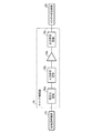
- FIG. 1 is a configuration diagram showing a Doherty amplifier 10 according to the first embodiment.
- the input terminal 1 is a terminal for inputting a signal to be amplified from the outside of the Doherty amplifier 10.
- the load 2 is an external load of the Doherty amplifier 10. One end of the load 2 is connected to the other end of the output matching circuit 22 described later of the Doherty amplifier 10, and the other end of the load 2 is grounded.
- the Doherty amplifier 10 amplifies the signal input from the input terminal 1 and outputs the amplified signal to the load 2.
- the power of the signal input from the input terminal 1 is P 1 .
- the Wilkinson distributor 11 includes a first transmission line 12, a second transmission line 13, and a resistor 14.
- Wilkinson divider 11 distributes the power P 1 of the input signal from the input terminal 1 into two.
- the Wilkinson distributor 11 outputs the first signal as one signal after distribution from the output terminal 11a to the phase adjustment line 15 described later, and the second signal from the output terminal 11b as the other signal after distribution.
- the signal is output to the coefficient adjusting line 16 described later.
- the first transmission line 12 has an electric length of a quarter wavelength (hereinafter, referred to as “ ⁇ / 4”) at the frequency of the signal input from the input terminal 1.
- the electric length of ⁇ / 4 is 90 degrees.
- the characteristic impedance of the first transmission line 12 is Z 2 .
- One end of the second transmission line 13 is connected to the input terminal 1, and the other end of the second transmission line 13 is connected to the other end of the resistor 14 and the output terminal 11b, respectively.
- the second transmission line 13 has an electrical length of ⁇ / 4 at the frequency of the signal input from the input terminal 1.
- the characteristic impedance of the second transmission line 13 is Z 3 .
- the ratio Z 3 / Z 2 of the characteristic impedance Z 3 of the second transmission line 13 to the characteristic impedance Z 2 of the first transmission line 12 is when both the carrier amplifier 18 and the peak amplifier 19 described later are saturated.
- P 2 is the power of the signal output from the output terminal 11a when the carrier amplifier 18 is saturated.
- P 3 is the power of the signal output from the output terminal 11b when the peak amplifier 19 is saturated.
- the resistor 14 is connected between the other end of the first transmission line 12 and the other end of the second transmission line 13.
- Resistance R iso resistor 14, the input impedance Z cin0 of the carrier amplifier 18 when the carrier amplifier 18 is saturated, the sum of the input impedance Z PIN0 of the peak amplifier 19 when the peak amplifier 19 is saturated, from 1 Is also a value multiplied by a proportional coefficient w of 0 or more, which is small.
- the input impedance Z sin0 of the carrier amplifier 18 when the carrier amplifier 18 is saturated may be referred to as an input impedance during the saturation operation of the carrier amplifier 18.
- the input impedance Z pin0 of the peak amplifier 19 when the peak amplifier 19 is saturated may be referred to as the input impedance during the saturation operation of the peak amplifier 19.
- the amplification operation of the carrier amplifier 18 with respect to the first signal is saturated, and when the peak amplifier 19 is saturated, the amplification operation of the peak amplifier 19 with respect to the second signal is performed. It is a time when it is saturated.
- phase adjustment line 15 is connected to each of the other end of the first transmission line 12 and one end of the resistor 14 via the output terminal 11a, and the other end of the phase adjustment line 15 is the carrier amplifier 18. It is connected to the input side.
- the phase adjusting line 15 has the same electric length as that of the coefficient adjusting line 16. The same electric length here is not limited to those having exactly the same electric length, but is a concept including those having different electric lengths within a range where there is no practical problem.
- the characteristic impedance of the phase adjustment line 15 is the same as the input impedance Z sin 0 of the carrier amplifier 18.
- the same here is not limited to the one in which the characteristic impedance of the phase adjustment line 15 and the input impedance Z sin0 of the carrier amplifier 18 are exactly the same, and also include those which are different within a range where there is no practical problem. Is a concept.
- the coefficient adjusting line 16 is connected to the other end of the second transmission line 13 and the other end of the resistor 14 via the output terminal 11b, and the other end of the coefficient adjusting line 16 has a phase described later. It is connected to one end of the adjustment line 17.
- the coefficient adjusting line 16 is a line for adjusting the reflection coefficient ⁇ pin of the second signal in the peak amplifier 19 when the peak amplifier 19 is viewed from the other end of the second transmission line 13.
- One end of the phase adjustment line 17 is connected to the other end of the coefficient adjustment line 16, and the other end of the phase adjustment line 17 is connected to the input side of the peak amplifier 19.
- the phase adjusting line 17 has an electric length of ⁇ / 4 at the frequency of the signal input from the input terminal 1.
- Each of the characteristic impedance of the coefficient adjusting line 16 and the characteristic impedance of the phase adjusting line 17 is the same as the input impedance Z pin 0 at the time of saturation operation of the peak amplifier 19.
- the same here is not limited to those having exactly the same impedance, but is a concept that includes impedances having different impedances within a range where there is no practical problem.
- the input side of the carrier amplifier 18 is connected to the other end of the phase adjustment line 15, and the output side of the carrier amplifier 18 is connected to one end of the quarter wavelength line 20 described later.
- the carrier amplifier 18 amplifies the first signal that has passed through the phase adjustment line 15 after being output from the other end of the first transmission line 12, and a quarter wavelength of the amplified first signal. It is output to the output synthesis point 21 via the line 20. Since the carrier amplifier 18 is biased to class AB, the input impedance Z sin0 of the carrier amplifier 18 does not change from the linear operation to the saturation operation. During the linear operation, the carrier amplifier 18 starts the amplification operation for the first signal, and during the linear operation, the peak amplifier 19 does not start the amplification operation for the second signal.
- the saturation operation of the carrier amplifier 18 and the saturation operation of the peak amplifier 19 occur at the same time. Simultaneous here is not limited to those in which the occurrence times during the saturation operation are exactly the same, but is a concept that includes those in which the saturation operations are different within a range where there is no practical problem.
- FIG. 2 is a configuration diagram showing the inside of the carrier amplifier 18.
- the carrier amplifier 18 is connected to an input matching circuit 18b connected to the input side of the transistor 18a and an output side of the transistor 18a in addition to the transistor 18a that amplifies the first signal. It is provided with an output matching circuit 18c.
- the carrier amplifier 18 blocks the passage of frequency components other than the desired frequency component contained in the first signal, and provides a stabilizing circuit 18d for passing the desired frequency component.
- the stabilizing circuit 18d is connected between the phase adjusting line 15 and the input matching circuit 18b, and is realized by, for example, a low-pass filter, a band-pass filter, or a high-pass filter.
- the stabilization circuit 18d is connected between the phase adjustment line 15 and the input matching circuit 18b.
- the stabilizing circuit 18d is used between the input matching circuit 18b and the transistor 18a, between the transistor 18a and the output matching circuit 18c, or between the output matching circuit 18c and the quarter wavelength line. It may be connected to 20.
- the input side of the peak amplifier 19 is connected to the other end of the phase adjustment line 17, and the output side of the peak amplifier 19 is connected to the output synthesis point 21.
- the peak amplifier 19 amplifies the second signal that has been output from the other end of the second transmission line 13 and then has passed through each of the coefficient adjustment line 16 and the phase adjustment line 17, and the second signal after amplification is amplified. Is output to the output synthesis point 21. Since the peak amplifier 19 is biased to class C, the input impedance Z pin0 of the peak amplifier 19 changes significantly from the linear operation to the saturation operation.
- FIG. 3 is a configuration diagram showing the inside of the peak amplifier 19.
- the peak amplifier 19 is connected to the input matching circuit 19b connected to the input side of the transistor 19a and the output side of the transistor 19a, in addition to the transistor 19a that amplifies the second signal. It is provided with an output matching circuit 19c.
- the peak amplifier 19 blocks the passage of frequency components other than the desired frequency component contained in the second signal, and provides a stabilizing circuit 19d that allows the desired frequency component to pass through. I have.
- the stabilizing circuit 19d is connected between the phase adjusting line 17 and the input matching circuit 19b, and is realized by, for example, a low-pass filter, a band-pass filter, or a high-pass filter.
- the stabilization circuit 19d is connected between the phase adjustment line 17 and the input matching circuit 19b.
- the stabilizing circuit 19d is used between the input matching circuit 19b and the transistor 19a, between the transistor 19a and the output matching circuit 19c, or between the output matching circuit 19c and the output synthesis point 21. It may be connected in between.
- the quarter wavelength line 20 is connected to the output side of the carrier amplifier 18, and the other end of the quarter wavelength line 20 is connected to the output synthesis point 21.
- the quarter wavelength line 20 has an electrical length of ⁇ / 4 at the frequency of the signal input from the input terminal 1.
- the quarter wavelength line 20 is connected between the carrier amplifier 18 and the output synthesis point 21 in order to modulate the impedance at the time of backoff.
- the output side of the peak amplifier 19 and the other end of the quarter wavelength line 20 are connected to the output synthesis point 21.
- the first signal after amplification that has passed through the quarter wavelength line 20 after being output from the carrier amplifier 18 and the second signal after amplification that has been output from the peak amplifier 19 are the output synthesis points 21. Is synthesized in phase.
- One end of the output matching circuit 22 is connected to the output synthesis point 21, and the other end of the output matching circuit 22 is connected to the load 2.
- the output matching circuit 22 is provided to match the impedance on the output side of the Doherty amplifier 10 with the impedance of the load 2.
- the input impedance Z sin0 of the carrier amplifier 18 does not change from the linear operation to the saturation operation.
- the characteristic impedance of the phase adjustment line 15 is the same as the input impedance Z sin 0 of the carrier amplifier 18 from the linear operation to the saturation operation of the carrier amplifier 18. Therefore, the absolute value of the input reflection when the carrier amplifier 18 is viewed from the output terminal 11a of the Wilkinson distributor 11 is 0 from the linear operation to the saturation operation of the carrier amplifier 18.
- Each of the characteristic impedance of the coefficient adjusting line 16 and the characteristic impedance of the phase adjusting line 17 is the same as the input impedance Z pin 0 at the time of saturation operation in the peak amplifier 19.
- the peak amplifier 19 is biased to class C, so that the input impedance Z pin0 of the peak amplifier 19 changes significantly from the linear operation to the saturation operation. Therefore, the characteristic impedance of the coefficient adjusting line 16 and the characteristic impedance of the phase adjusting line 17 are different from the input impedance Z pin 0 of the peak amplifier 19 except when the operation of the peak amplifier 19 is saturated.
- FIG. 4 is a Smith chart showing the input reflection of the peak amplifier 19 from the operation of the Doherty amplifier 10 shown in FIG. 1 from the linear operation to the saturation operation.
- the input reflection of the peak amplifier 19 shown in FIG. 4 is a view of the peak amplifier 19 from the input side of the coefficient adjusting line 16.
- the impedance at the center of the Smith chart shown in FIG. 4 is the input impedance Z pin 0 when the operation of the peak amplifier 19 is the saturated operation.
- the impedance at the center of the Smith chart shown in FIG. 4 is expressed as 1.0 because the operation of the peak amplifier 19 is standardized by the input impedance Z pin0 when the operation is saturated.
- the absolute value of the input reflection of the peak amplifier 19 is 0 as shown in FIG.
- the absolute value of the input reflection of the peak amplifier 19 is not 0 but a value close to 1 as shown in FIG.
- FIG. 5 is a Smith chart showing the input reflection of the peak amplifier 19 from the operation of the Doherty amplifier 10 shown in FIG. 1 from the linear operation to the saturation operation.
- FIG. 5 illustrates the input reflection of the peak amplifier 19 when the electrical lengths of the coefficient adjusting line 16 are 0 degrees, 30 degrees, 60 degrees, 90 degrees, 120 degrees and 150 degrees.
- the input reflection of the peak amplifier 19 when the electric length of the coefficient adjusting line 16 is 0 degrees is the same as the input reflection of the peak amplifier 19 shown in FIG. Since each of the characteristic impedance of the coefficient adjustment line 16 and the characteristic impedance of the phase adjustment line 17 is the same as the input impedance Z pin 0 during the saturation operation of the peak amplifier 19 even if the electrical length of the coefficient adjustment line 16 changes.
- the phase of the input reflection during the linear operation of the peak amplifier 19 changes. Therefore, as shown in FIG. 5, the input reflection of the peak amplifier 19 when the peak amplifier 19 is viewed from the input side of the coefficient adjustment line 16 rotates on the Smith chart according to the electric length of the coefficient adjustment line 16.
- the phase of the input reflection of the peak amplifier 19 changes depending on the type of the transistor 19a included in the peak amplifier 19 or the types of the input matching circuit 19b and the output matching circuit 19c.
- the ideal operation is an operation that satisfies the following two conditions.
- Condition (1) After the carrier amplifier 18 starts the signal amplification operation before the peak amplifier 19, the peak amplifier 19 suddenly starts the signal amplification operation from the back-off operation between the linear operation and the saturation operation. ..
- Condition (2) The saturation operation of the carrier amplifier 18 and the saturation operation of the peak amplifier 19 occur at the same time.
- the range 30 of the input reflection phase shown in FIG. 5 is the input reflection phase when the peak amplifier 19 is viewed from the output terminal 11b of the Wilkinson distributor 11, which is necessary for realizing the ideal operation of the Doherty amplifier 10 shown in FIG. It is in the range of, and is already a value at the time of designing the Doherty amplifier 10 shown in FIG.
- the range 30 of the input reflection phase when the peak amplifier 19 is viewed from the output terminal 11b shown in FIG. 1 is in the range of 135 degrees to 220 degrees.
- the phase of the input reflection of the peak amplifier 19 is 120 degrees, the phase of the input reflection of the peak amplifier 19 is included in the range 30 of the input reflection phase of the Doherty amplifier 10.
- the input reflection phase of the peak amplifier 19 is included in the input reflection phase range 30 at the time of designing the Doherty amplifier 10 or the like.
- the electrical length of the coefficient adjusting line 16 is set.
- the resistance value Riso of the resistor 14 is set when the operation of the carrier amplifier 18 is saturated.
- the input impedance Z cin0, input impedance to the sum of the Z PIN0, small 0 or more proportional coefficient w than 1 is in the multiplied value when operation of the peak amplifier 19 is at saturation operation.
- the Wilkinson distributor 11 distributes the power P 1 of the input signal into two.
- the Wilkinson distributor 11 outputs a first signal from the output terminal 11a as one signal after distribution to the carrier amplifier 18 via the phase adjustment line 15. Further, the Wilkinson distributor 11 outputs a second signal from the output terminal 11b as the other signal after distribution to the peak amplifier 19 via the coefficient adjusting line 16 and the phase adjusting line 17. Details of the operation of the Wilkinson distributor 11 will be described later.
- the carrier amplifier 18 amplifies the first signal that has passed through the phase adjustment line 15 after being output from the output terminal 11a of the Wilkinson distributor 11.
- the carrier amplifier 18 outputs the first signal after amplification to the output synthesis point 21 via the quarter wavelength line 20.
- the peak amplifier 19 amplifies the second signal that has been output from the output terminal 11b of the Wilkinson distributor 11 and then has passed through each of the coefficient adjusting line 16 and the phase adjusting line 17.
- the peak amplifier 19 amplifies the second signal and outputs the amplified second signal to the output synthesis point 21.
- the first signal after amplification that has passed through the quarter wavelength line 20 after being output from the carrier amplifier 18 and the second signal after amplification that has been output from the peak amplifier 19 are synthesized in phase.
- the combined signal at the output synthesis point 21 (hereinafter referred to as “combined signal”) is output to the load 2 via the output matching circuit 22.
- FIG. 6 is a configuration diagram showing details of the Wilkinson distributor 11.
- I 1 is the current of the signal input from the input terminal 1
- V 1 is the voltage of the signal input from the input terminal 1.
- Z in is the input impedance of the Doherty amplifier 10 shown in FIG. 1
- ⁇ in is the reflection coefficient of the input signal in the Doherty amplifier 10 when the inside of the Doherty amplifier 10 is viewed from the input terminal 1.
- I 2 ( ⁇ / 4) is the current of the signal input to the first transmission line 12
- V 2 ( ⁇ / 4) is the voltage of the signal input to the first transmission line 12.
- I 2 (0) is the current of the signal output from the first transmission line 12, and V 2 (0) is the voltage of the signal output from the first transmission line 12.
- I 3 ( ⁇ / 4) is the current of the signal input to the second transmission line 13, and V 3 ( ⁇ / 4) is the voltage of the signal input to the second transmission line 13.
- I 3 (0) is the current of the signal output from the second transmission line 13, and V 3 (0) is the voltage of the signal output from the second transmission line 13.
- I iso is the current flowing through the resistor 14
- I 2 (0) -I iso is the current of the signal output from the output terminal 11a to the phase adjustment line 15
- I 3 (0) + I iso is the coefficient from the output terminal 11b. This is the current of the signal output to the adjustment line 16.
- Z cin is the impedance when the carrier amplifier 18 is seen from the output terminal 11a
- ⁇ cin is the reflection coefficient of the first signal in the carrier amplifier 18 when the carrier amplifier 18 is seen from the output terminal 11a.
- the Z pin is the impedance when the peak amplifier 19 is viewed from the output terminal 11b
- the ⁇ pin is the reflection coefficient of the second signal in the peak amplifier 19 when the peak amplifier 19 is viewed from the output terminal 11b.
- the ratio Z 3 / Z 2 of the characteristic impedance Z 3 of the second transmission line 13 to the characteristic impedance Z 2 of the first transmission line 12 and the carrier amplifier 18 and the ratio Z pin0 / Z cin0 of the input impedance Z PIN0 of the peak amplifier 19 to the input impedance Z cin0 of the relationship between the power distribution ratio P 2 / P 3 can be expressed as the following equation (3).
- the input impedance Z in of the Doherty amplifier 10 and the input impedance Z sin 0 at the time of saturation operation in the carrier amplifier 18 are already values. Therefore, the characteristic impedance Z 2 of the first transmission line 12 can be obtained by substituting the input impedance Z in and the input impedance Z sin 0 into the following equation (4).
- the characteristic impedance Z 3 of the second transmission line 13 can be obtained by substituting the characteristic impedance Z 2 of the first transmission line 12 into the following equation (5).
- resistance R iso a resistor 14, as shown in the following equation (6), if consistent with the sum of the input impedance Z cin0 and the input impedance Z PIN0, no current flows through resistor 14, output terminal The 11a and the output terminal 11b are isolated.
- the power distribution ratio P 2 / P 3 changes when the operation of the Doherty amplifier 10 shown in FIG. 1 is other than the saturation operation.
- the power distribution ratio P 2 / P 3 is unchanged, the desired power distribution ratio 1 / Consistent with K 2.
- the power distribution ratio P 2 / P 3 from the linear operation to the saturated operation of the Doherty amplifier 10 is expressed by the following equation (8). As shown in the equation (8), the power distribution ratio P 2 / P 3 from the linear operation to the saturation operation of the Doherty amplifier 10 changes depending on the proportional coefficient w.
- FIG. 7 shows 0.2 from 0.2 to 1.8 when the phase of the reflection coefficient ⁇ pin when the peak amplifier 19 is viewed from the output terminal 11b of the Wilkinson distributor 11 is 180 degrees.
- the horizontal axis is the absolute value of the input reflection of the peak amplifier 19, and when the absolute value of the input reflection is 0, the peak amplifier 19 is saturated. During linear operation of the peak amplifier 19, the absolute value of the input reflection is close to 1.
- the vertical axis is the normalized power distribution ratio in the range from the linear operation to the saturation operation of the Doherty amplifier 10.
- the standardized power distribution ratio is a power distribution ratio P 2 / P 3 standardized by 1 / K 2. Therefore, when the standardized power distribution ratio is 1, the power distribution ratio P 2 / P 3 is 1 / K 2 .
- the proportional coefficient w is 1 or more, as shown in FIG. 7, the normalized power distribution ratio is always 1 or more regardless of the absolute value of the input reflection of the peak amplifier 19, and the operation of the Doherty amplifier 10 is linear operation. From time to saturation operation, more power is distributed to the carrier amplifier 18 than to the peak amplifier 19. Therefore, when the proportional coefficient w is 1 or more, it is difficult to suddenly start the operation of the peak amplifier 19 at the time of backoff. Therefore, the carrier amplifier 18 may be saturated before the peak amplifier 19, and it is difficult to realize an ideal operation in which the carrier amplifier 18 and the peak amplifier 19 are saturated at the same time.
- the proportional coefficient w is smaller than 1, as shown in FIG. 7, there is an absolute value of the input reflection of the peak amplifier 19 in which the normalized power distribution ratio is smaller than 1.
- the proportional coefficient w is 0.4, as shown in FIG. 7, the normalized power distribution is in the range where the absolute value of the input reflection of the peak amplifier 19 is larger than 0 and smaller than about 0.72. The ratio is less than 1.
- the proportional coefficient w is 0.4, the absolute value of the input reflection of the peak amplifier 19 is smaller than 1, and when it is in the range of about 0.72 or more, the carrier amplifier 18 has more power than the peak amplifier 19. Is distributed. That is, from the linear operation to the back-off operation of the Doherty amplifier 10, more power is distributed to the carrier amplifier 18 than to the peak amplifier 19.
- the carrier amplifier 18 can start the signal amplification operation before the peak amplifier 19, and then the peak amplifier 19 can suddenly start the signal amplification operation.
- the power distribution ratio P 2 / P 3 becomes a desired power distribution ratio 1 / K 2 . That is, when the absolute value of the input reflection of the peak amplifier 19 is 0, both the carrier amplifier 18 and the peak amplifier 19 are saturated.
- FIG. 8 shows standardization when the proportional coefficient w is 0.4 and the phase of the reflection coefficient ⁇ pin of the second signal is changed in steps of 22.5 degrees from 0 degrees to 180 degrees. It is explanatory drawing which shows the power distribution ratio.
- the horizontal axis is the absolute value of the input reflection of the peak amplifier 19, and the vertical axis is the normalized power distribution ratio in the range from the linear operation to the saturation operation of the Doherty amplifier 10.
- the standardized power distribution ratio is a power distribution ratio P 2 / P 3 standardized by 1 / K 2.
- the reflection coefficient ⁇ pin There is an absolute value of the input reflection of the peak amplifier 19 that makes the standardized power distribution ratio less than 1 even when the phase of is in the range of 180 degrees to 225 degrees.
- the phase of the reflection coefficient ⁇ pin of the second signal is in the range of 270 degrees to 360 degrees, the normalized power distribution ratio becomes smaller than 1, and there is no absolute value of the input reflection of the peak amplifier 19. .. From the above, there is a phase condition of the reflection coefficient ⁇ pin that can realize the ideal operation of the Doherty amplifier 10.
- FIG. 9 is an explanatory diagram showing the gain with respect to the output power of the Doherty amplifier 10 that satisfies the phase condition of the reflection coefficient ⁇ pin that can realize the ideal operation and has the proportional coefficient w smaller than 1 and 0 or more.
- the Doherty amplifier described in Patent Document 1 since the peak amplifier cannot suddenly start the signal amplification operation at the time of backoff, the gain sharply decreases from the time of backoff to the saturation operation, and the gain characteristic. Becomes non-linear.
- the peak amplifier 19 can suddenly start the signal amplification operation at the time of backoff, the flatness of the gain from the backoff time to the saturation operation can be maintained. Further, in the Doherty amplifier 10 shown in FIG. 1, since the carrier amplifier 18 and the peak amplifier 19 can be saturated at the same time, the saturated output power is increased as compared with the Doherty amplifier described in Patent Document 1.
- the Doherty amplifier 10 shown in FIG. 1 does not include a control circuit as described in Patent Document 1, but prevents a decrease in the gain of the combined signal, and provides a delay circuit as described in Patent Document 1. You don't have to prepare. Therefore, the Doherty amplifier 10 shown in FIG. 1 does not have a problem that the amplified signal cannot be output from the time when the input signal is input to the delay circuit until the delay time of the delay circuit elapses.
- the Doherty amplifier 10 shown in FIG. 1 is smaller than the Doherty amplifier described in Patent Document 1 because it does not have a detection circuit, a control circuit, and a delay circuit as described in Patent Document 1. And simplification can be realized, and power consumption can be reduced.
- the ratio Z 3 / Z 2 of the characteristic impedance Z 3 of the second transmission line 13 to the characteristic impedance Z 2 of the first transmission line 12 determines both the carrier amplifier 18 and the peak amplifier 19.
- the power distribution ratio P 2 / P 3 of the signal to be amplified with respect to the carrier amplifier 18 and the peak amplifier 19 at the time of saturation, and the resistance value Riso of the resistor 14 is the carrier amplifier 18 when the carrier amplifier 18 is saturated.
- the Doherty amplifier 10 does not include a delay circuit that delays the signal to be amplified, and the signal output from the carrier amplifier 18 and the signal output from the peak amplifier 19 from the backoff time to the saturation operation. It is possible to prevent a decrease in the gain of the combined signal.
- the Wilkinson distributor 11 describes a Doherty amplifier 10 including capacitors 41 and 42 connected in series with the resistor 40.
- FIG. 10 is a configuration diagram showing a Wilkinson distributor 11 of the Doherty amplifier 10 according to the second embodiment.
- the resistor 40 has a parasitic inductance 40b in addition to the resistor 40a having a resistance value of Riso.
- One end of the capacitor 41 is connected to the other end of the first transmission line 12 and each of the output terminals 11a, and the other end of the capacitor 41 is connected to one end of the resistor 40.
- One end of the capacitor 42 is connected to the other end of the second transmission line 13 and each of the output terminals 11b, and the other end of the capacitor 42 is connected to the other end of the resistor 40.
- Each of the capacitor 41 and the capacitor 42 is provided to compensate for the phase rotation in the first signal and the second signal due to the resistance 40 having the parasitic inductance 40b. Since the Wilkinson distributor 11 includes capacitors 41 and 42 connected in series with the resistor 40, even if the resistor 40 has a parasitic inductance 40b, it is synthesized in the same manner as the Doherty amplifier 10 shown in FIG. It is possible to prevent a decrease in signal gain.
- FIG. 11 is a configuration diagram showing a communication device including the Doherty amplifier 10 shown in FIG.
- the Doherty amplifier shown in FIG. 1 does not include a delay circuit as described in Patent Document 1. Therefore, the communication device shown in FIG. 11 can amplify the communication signal without delaying the communication signal corresponding to the delay time of the delay circuit.
- the communication device shown in FIG. 11 includes the Doherty amplifier 10 shown in FIG. 1, but may include the Doherty amplifier 10 including the Wilkinson distributor 11 shown in FIG.
- This disclosure is suitable for Doherty amplifiers and communication devices.
Landscapes
- Engineering & Computer Science (AREA)
- Power Engineering (AREA)
- Amplifiers (AREA)
- Microwave Amplifiers (AREA)
Priority Applications (5)
| Application Number | Priority Date | Filing Date | Title |
|---|---|---|---|
| JP2021560365A JP7019882B2 (ja) | 2019-12-13 | 2019-12-13 | ドハティ増幅器及び通信装置 |
| CN201980102771.2A CN114747136B (zh) | 2019-12-13 | 2019-12-13 | 多尔蒂放大器和通信装置 |
| PCT/JP2019/048944 WO2021117222A1 (ja) | 2019-12-13 | 2019-12-13 | ドハティ増幅器及び通信装置 |
| EP19955647.3A EP4064557B1 (en) | 2019-12-13 | 2019-12-13 | Doherty amplifier and communication device |
| US17/722,839 US12328100B2 (en) | 2019-12-13 | 2022-04-18 | Doherty amplifier and communication device |
Applications Claiming Priority (1)
| Application Number | Priority Date | Filing Date | Title |
|---|---|---|---|
| PCT/JP2019/048944 WO2021117222A1 (ja) | 2019-12-13 | 2019-12-13 | ドハティ増幅器及び通信装置 |
Related Child Applications (1)
| Application Number | Title | Priority Date | Filing Date |
|---|---|---|---|
| US17/722,839 Continuation US12328100B2 (en) | 2019-12-13 | 2022-04-18 | Doherty amplifier and communication device |
Publications (1)
| Publication Number | Publication Date |
|---|---|
| WO2021117222A1 true WO2021117222A1 (ja) | 2021-06-17 |
Family
ID=76330098
Family Applications (1)
| Application Number | Title | Priority Date | Filing Date |
|---|---|---|---|
| PCT/JP2019/048944 Ceased WO2021117222A1 (ja) | 2019-12-13 | 2019-12-13 | ドハティ増幅器及び通信装置 |
Country Status (5)
| Country | Link |
|---|---|
| US (1) | US12328100B2 (https=) |
| EP (1) | EP4064557B1 (https=) |
| JP (1) | JP7019882B2 (https=) |
| CN (1) | CN114747136B (https=) |
| WO (1) | WO2021117222A1 (https=) |
Cited By (1)
| Publication number | Priority date | Publication date | Assignee | Title |
|---|---|---|---|---|
| WO2025177977A1 (ja) * | 2024-02-19 | 2025-08-28 | ヌヴォトンテクノロジージャパン株式会社 | ドハティ増幅器 |
Families Citing this family (2)
| Publication number | Priority date | Publication date | Assignee | Title |
|---|---|---|---|---|
| US12587140B2 (en) | 2022-02-01 | 2026-03-24 | Qorvo Us, Inc. | Barely Doherty et using et VCC modulation for bias control |
| US12587138B2 (en) * | 2022-05-12 | 2026-03-24 | Qorvo Us, Inc. | Asymmetrical power amplifier circuit |
Citations (8)
| Publication number | Priority date | Publication date | Assignee | Title |
|---|---|---|---|---|
| JPS55132104A (en) * | 1979-03-30 | 1980-10-14 | Nec Corp | Wilkinson type 90-degree hybrid |
| JPH07263981A (ja) * | 1994-03-17 | 1995-10-13 | Fujitsu Ltd | 電力増幅器 |
| JPH09321509A (ja) * | 1996-03-26 | 1997-12-12 | Matsushita Electric Ind Co Ltd | 分配器/合成器 |
| JP2006339981A (ja) * | 2005-06-01 | 2006-12-14 | Toshiba Corp | ドハティ増幅器 |
| JP2008125044A (ja) | 2006-10-17 | 2008-05-29 | Hitachi Kokusai Electric Inc | 増幅器 |
| JP2011211679A (ja) * | 2010-03-10 | 2011-10-20 | Toyama Univ | 信号分配回路の設計方法、信号分配器の設計方法、信号分配回路の設計プログラム、及び信号分配器の設計プログラム |
| JP2017534228A (ja) * | 2014-11-05 | 2017-11-16 | クゥアルコム・インコーポレイテッドQualcomm Incorporated | 動的電力ディバイダ回路および方法 |
| JP2018186370A (ja) * | 2017-04-25 | 2018-11-22 | 日本アンテナ株式会社 | ウィルキンソン回路 |
Family Cites Families (6)
| Publication number | Priority date | Publication date | Assignee | Title |
|---|---|---|---|---|
| JP5217182B2 (ja) * | 2007-02-22 | 2013-06-19 | 富士通株式会社 | 高周波増幅回路 |
| CN101836357A (zh) * | 2007-11-21 | 2010-09-15 | 富士通株式会社 | 功率放大器 |
| JP2009182635A (ja) * | 2008-01-30 | 2009-08-13 | Toshiba Corp | ドハティ増幅器 |
| WO2009151973A2 (en) * | 2008-05-28 | 2009-12-17 | Rayspan Corporation | Power amplifier architectures |
| CN111313841B (zh) * | 2014-12-18 | 2023-09-12 | 株式会社东芝 | 多尔蒂型放大器 |
| JP2020184749A (ja) * | 2019-04-05 | 2020-11-12 | 住友電工デバイス・イノベーション株式会社 | 集積ドハティ増幅器 |
-
2019
- 2019-12-13 JP JP2021560365A patent/JP7019882B2/ja active Active
- 2019-12-13 CN CN201980102771.2A patent/CN114747136B/zh active Active
- 2019-12-13 EP EP19955647.3A patent/EP4064557B1/en active Active
- 2019-12-13 WO PCT/JP2019/048944 patent/WO2021117222A1/ja not_active Ceased
-
2022
- 2022-04-18 US US17/722,839 patent/US12328100B2/en active Active
Patent Citations (8)
| Publication number | Priority date | Publication date | Assignee | Title |
|---|---|---|---|---|
| JPS55132104A (en) * | 1979-03-30 | 1980-10-14 | Nec Corp | Wilkinson type 90-degree hybrid |
| JPH07263981A (ja) * | 1994-03-17 | 1995-10-13 | Fujitsu Ltd | 電力増幅器 |
| JPH09321509A (ja) * | 1996-03-26 | 1997-12-12 | Matsushita Electric Ind Co Ltd | 分配器/合成器 |
| JP2006339981A (ja) * | 2005-06-01 | 2006-12-14 | Toshiba Corp | ドハティ増幅器 |
| JP2008125044A (ja) | 2006-10-17 | 2008-05-29 | Hitachi Kokusai Electric Inc | 増幅器 |
| JP2011211679A (ja) * | 2010-03-10 | 2011-10-20 | Toyama Univ | 信号分配回路の設計方法、信号分配器の設計方法、信号分配回路の設計プログラム、及び信号分配器の設計プログラム |
| JP2017534228A (ja) * | 2014-11-05 | 2017-11-16 | クゥアルコム・インコーポレイテッドQualcomm Incorporated | 動的電力ディバイダ回路および方法 |
| JP2018186370A (ja) * | 2017-04-25 | 2018-11-22 | 日本アンテナ株式会社 | ウィルキンソン回路 |
Non-Patent Citations (1)
| Title |
|---|
| See also references of EP4064557A4 |
Cited By (1)
| Publication number | Priority date | Publication date | Assignee | Title |
|---|---|---|---|---|
| WO2025177977A1 (ja) * | 2024-02-19 | 2025-08-28 | ヌヴォトンテクノロジージャパン株式会社 | ドハティ増幅器 |
Also Published As
| Publication number | Publication date |
|---|---|
| EP4064557B1 (en) | 2024-05-08 |
| CN114747136A (zh) | 2022-07-12 |
| EP4064557A1 (en) | 2022-09-28 |
| JP7019882B2 (ja) | 2022-02-15 |
| CN114747136B (zh) | 2025-04-15 |
| US20220239259A1 (en) | 2022-07-28 |
| JPWO2021117222A1 (https=) | 2021-06-17 |
| US12328100B2 (en) | 2025-06-10 |
| EP4064557A4 (en) | 2022-11-09 |
Similar Documents
| Publication | Publication Date | Title |
|---|---|---|
| CN108259008B (zh) | 具有无源相位补偿电路的多尔蒂放大器 | |
| JP7019882B2 (ja) | ドハティ増幅器及び通信装置 | |
| US10608594B2 (en) | Doherty amplifier | |
| RU2617508C2 (ru) | Система управления усилителем мощности | |
| JP6513225B2 (ja) | ドハティ増幅器 | |
| JP2004173231A (ja) | ドハティ増幅器を用いた信号増幅装置 | |
| JP2008167434A (ja) | 調整可能な振幅および形状を備えたプリディストーション線形化装置 | |
| JP2006173722A (ja) | 高周波用のドハティ型の高効率増幅器、およびその信号処理方法 | |
| KR20130123305A (ko) | 도허티 증폭기 | |
| JP4627457B2 (ja) | 増幅器 | |
| US7183843B1 (en) | Electronically tuned power amplifier | |
| US6646504B2 (en) | Broadband amplifier system having improved linearity and minimum loss | |
| JP5152512B2 (ja) | プローブ | |
| JP2016063291A (ja) | 広帯域増幅器 | |
| WO2019207700A1 (ja) | 増幅器 | |
| CN115804007A (zh) | 多尔蒂放大器 | |
| CN113875150A (zh) | 多赫蒂放大器和通信装置 | |
| JP2007288545A (ja) | 前置歪補償回路 | |
| JP2007129426A (ja) | 高周波電力増幅器 | |
| JP5251285B2 (ja) | 半導体集積回路装置及びオフセットキャンセル設定システム | |
| US7518468B2 (en) | Power divider-combiner circuit | |
| JP2007124038A (ja) | 高周波増幅器 | |
| JP2005151185A (ja) | 高出力広帯域信号を合成する方法及び増幅器 | |
| JP2018142766A (ja) | 増幅回路 | |
| JP2002111395A (ja) | 高周波増幅装置 |
Legal Events
| Date | Code | Title | Description |
|---|---|---|---|
| 121 | Ep: the epo has been informed by wipo that ep was designated in this application |
Ref document number: 19955647 Country of ref document: EP Kind code of ref document: A1 |
|
| ENP | Entry into the national phase |
Ref document number: 2021560365 Country of ref document: JP Kind code of ref document: A |
|
| ENP | Entry into the national phase |
Ref document number: 2019955647 Country of ref document: EP Effective date: 20220624 |
|
| NENP | Non-entry into the national phase |
Ref country code: DE |
|
| WWG | Wipo information: grant in national office |
Ref document number: 201980102771.2 Country of ref document: CN |