WO2021100798A1 - 樹脂パネル及び赤外線センサー - Google Patents
樹脂パネル及び赤外線センサー Download PDFInfo
- Publication number
- WO2021100798A1 WO2021100798A1 PCT/JP2020/043155 JP2020043155W WO2021100798A1 WO 2021100798 A1 WO2021100798 A1 WO 2021100798A1 JP 2020043155 W JP2020043155 W JP 2020043155W WO 2021100798 A1 WO2021100798 A1 WO 2021100798A1
- Authority
- WO
- WIPO (PCT)
- Prior art keywords
- layer
- resin
- resin panel
- refractive index
- core layer
- Prior art date
- Legal status (The legal status is an assumption and is not a legal conclusion. Google has not performed a legal analysis and makes no representation as to the accuracy of the status listed.)
- Ceased
Links
Images


Classifications
-
- G—PHYSICS
- G01—MEASURING; TESTING
- G01J—MEASUREMENT OF INTENSITY, VELOCITY, SPECTRAL CONTENT, POLARISATION, PHASE OR PULSE CHARACTERISTICS OF INFRARED, VISIBLE OR ULTRAVIOLET LIGHT; COLORIMETRY; RADIATION PYROMETRY
- G01J3/00—Spectrometry; Spectrophotometry; Monochromators; Measuring colours
- G01J3/02—Details
- G01J3/10—Arrangements of light sources specially adapted for spectrometry or colorimetry
- G01J3/108—Arrangements of light sources specially adapted for spectrometry or colorimetry for measurement in the infrared range
-
- G—PHYSICS
- G01—MEASURING; TESTING
- G01J—MEASUREMENT OF INTENSITY, VELOCITY, SPECTRAL CONTENT, POLARISATION, PHASE OR PULSE CHARACTERISTICS OF INFRARED, VISIBLE OR ULTRAVIOLET LIGHT; COLORIMETRY; RADIATION PYROMETRY
- G01J5/00—Radiation pyrometry, e.g. infrared or optical thermometry
- G01J5/02—Constructional details
- G01J5/04—Casings
- G01J5/048—Protective parts
-
- B—PERFORMING OPERATIONS; TRANSPORTING
- B32—LAYERED PRODUCTS
- B32B—LAYERED PRODUCTS, i.e. PRODUCTS BUILT-UP OF STRATA OF FLAT OR NON-FLAT, e.g. CELLULAR OR HONEYCOMB, FORM
- B32B27/00—Layered products comprising a layer of synthetic resin
- B32B27/14—Layered products comprising a layer of synthetic resin next to a particulate layer
-
- B—PERFORMING OPERATIONS; TRANSPORTING
- B32—LAYERED PRODUCTS
- B32B—LAYERED PRODUCTS, i.e. PRODUCTS BUILT-UP OF STRATA OF FLAT OR NON-FLAT, e.g. CELLULAR OR HONEYCOMB, FORM
- B32B7/00—Layered products characterised by the relation between layers; Layered products characterised by the relative orientation of features between layers, or by the relative values of a measurable parameter between layers, i.e. products comprising layers having different physical, chemical or physicochemical properties; Layered products characterised by the interconnection of layers
- B32B7/02—Physical, chemical or physicochemical properties
- B32B7/023—Optical properties
-
- G—PHYSICS
- G01—MEASURING; TESTING
- G01J—MEASUREMENT OF INTENSITY, VELOCITY, SPECTRAL CONTENT, POLARISATION, PHASE OR PULSE CHARACTERISTICS OF INFRARED, VISIBLE OR ULTRAVIOLET LIGHT; COLORIMETRY; RADIATION PYROMETRY
- G01J5/00—Radiation pyrometry, e.g. infrared or optical thermometry
- G01J5/02—Constructional details
- G01J5/08—Optical arrangements
- G01J5/0875—Windows; Arrangements for fastening thereof
-
- G—PHYSICS
- G01—MEASURING; TESTING
- G01S—RADIO DIRECTION-FINDING; RADIO NAVIGATION; DETERMINING DISTANCE OR VELOCITY BY USE OF RADIO WAVES; LOCATING OR PRESENCE-DETECTING BY USE OF THE REFLECTION OR RERADIATION OF RADIO WAVES; ANALOGOUS ARRANGEMENTS USING OTHER WAVES
- G01S17/00—Systems using the reflection or reradiation of electromagnetic waves other than radio waves, e.g. lidar systems
- G01S17/88—Lidar systems specially adapted for specific applications
- G01S17/93—Lidar systems specially adapted for specific applications for anti-collision purposes
- G01S17/931—Lidar systems specially adapted for specific applications for anti-collision purposes of land vehicles
-
- G—PHYSICS
- G01—MEASURING; TESTING
- G01S—RADIO DIRECTION-FINDING; RADIO NAVIGATION; DETERMINING DISTANCE OR VELOCITY BY USE OF RADIO WAVES; LOCATING OR PRESENCE-DETECTING BY USE OF THE REFLECTION OR RERADIATION OF RADIO WAVES; ANALOGOUS ARRANGEMENTS USING OTHER WAVES
- G01S7/00—Details of systems according to groups G01S13/00, G01S15/00, G01S17/00
- G01S7/48—Details of systems according to groups G01S13/00, G01S15/00, G01S17/00 of systems according to group G01S17/00
- G01S7/481—Constructional features, e.g. arrangements of optical elements
-
- G—PHYSICS
- G02—OPTICS
- G02B—OPTICAL ELEMENTS, SYSTEMS OR APPARATUS
- G02B1/00—Optical elements characterised by the material of which they are made; Optical coatings for optical elements
- G02B1/10—Optical coatings produced by application to, or surface treatment of, optical elements
- G02B1/11—Anti-reflection coatings
- G02B1/111—Anti-reflection coatings using layers comprising organic materials
-
- G—PHYSICS
- G02—OPTICS
- G02B—OPTICAL ELEMENTS, SYSTEMS OR APPARATUS
- G02B5/00—Optical elements other than lenses
- G02B5/20—Filters
- G02B5/208—Filters for use with infrared or ultraviolet radiation, e.g. for separating visible light from infrared and/or ultraviolet radiation
-
- G—PHYSICS
- G02—OPTICS
- G02B—OPTICAL ELEMENTS, SYSTEMS OR APPARATUS
- G02B5/00—Optical elements other than lenses
- G02B5/20—Filters
- G02B5/22—Absorbing filters
- G02B5/223—Absorbing filters containing organic substances, e.g. dyes, inks or pigments
-
- G—PHYSICS
- G01—MEASURING; TESTING
- G01S—RADIO DIRECTION-FINDING; RADIO NAVIGATION; DETERMINING DISTANCE OR VELOCITY BY USE OF RADIO WAVES; LOCATING OR PRESENCE-DETECTING BY USE OF THE REFLECTION OR RERADIATION OF RADIO WAVES; ANALOGOUS ARRANGEMENTS USING OTHER WAVES
- G01S7/00—Details of systems according to groups G01S13/00, G01S15/00, G01S17/00
- G01S7/48—Details of systems according to groups G01S13/00, G01S15/00, G01S17/00 of systems according to group G01S17/00
- G01S7/481—Constructional features, e.g. arrangements of optical elements
- G01S7/4811—Constructional features, e.g. arrangements of optical elements common to transmitter and receiver
Definitions
- the present invention relates to a resin panel and an infrared sensor.
- a protective cover may be arranged in front of the light emitting element and the light receiving element.
- the protective cover of the optical sensor is formed, for example, to protect the light emitting element and the light receiving element from flying stones, sunlight, wind and rain, and the like. Therefore, it is preferable that the protective cover has excellent impact resistance and weather resistance.
- Patent Document 1 proposes arranging an optical element made of polycarbonate as a protective cover.
- Some light emitting elements of an optical sensor use light in the infrared region as an emission wavelength in order to suppress the influence on the human eye.
- many of the light emitting elements of optical sensors mainly LiDAR
- many of the light emitting elements of optical sensors (mainly LiDAR) mounted on automobiles use light in the infrared region as the light emitting wavelength.
- an optical element made of polycarbonate disclosed in Patent Document 1 is applied as a protective cover for an optical sensor (infrared sensor) whose emission wavelength is light in the infrared region, the infrared sensor often does not function sufficiently. ..
- a design layer is applied to the protective cover in order to enhance the design, there is a tendency that the infrared sensor does not function sufficiently in many cases.
- An object of the present invention is to provide a resin panel capable of fully functioning the infrared sensor when applied as a protective cover for the infrared sensor, and an infrared sensor having the resin panel.
- the present invention provides the following [1] to [2].
- [1] A resin panel having at least a core layer, wherein the resin panel has a light transmittance of 85% or more and a visible light transmittance of 20% or less at a wavelength of 905 nm.
- An infrared sensor having an infrared light emitting element, an infrared light receiving element, and a protective cover arranged in front of the infrared light emitting element and the infrared light receiving element, wherein the protective cover is the resin of the above [1].
- An infrared sensor that is a panel.
- the resin panel of the present invention can fully function the infrared sensor when applied as a protective cover for the infrared sensor.
- the infrared sensor of the present invention having the resin panel can fully function the infrared sensor.
- the resin panel of the present invention is a resin panel having at least a core layer, and the resin panel has a light transmittance of 85% or more and a visible light transmittance of 20% or less at a wavelength of 905 nm.
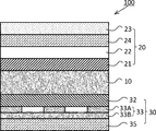
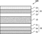
- FIGS. 1 to 6 are cross-sectional views showing an embodiment of the resin panel of the present invention.
- Each of the resin panels (100) shown in FIGS. 1 to 6 has a core layer (10).
- the resin panels (100) of FIGS. 1 to 6 have an inner layer (20) in addition to the core layer (10), and have an antireflection layer (23) and the like as the inner layer (20). doing.
- the resin panels (100) of FIGS. 1 to 5 have an outer layer (30) in addition to the core layer (10), and the hard coat layer B (35) or the like is used as the outer layer (30).
- the resin panels (100) of FIGS. 1 to 5 have an outer layer (30) in addition to the core layer (10), and the hard coat layer B (35) or the like is used as the outer layer (30).
- the "inner layer” means a layer located on the infrared emitting element and the infrared receiving element side with respect to the core layer when the resin panel is applied as a protective cover for the infrared sensor.
- the “outer layer” is a layer located on the opposite side of the infrared light emitting element and the infrared light receiving element with respect to the core layer when the resin panel is applied as a protective cover for the infrared sensor. Means that.
- the resin panel of the present invention is required to have a light transmittance of 85% or more at a wavelength of 905 nm and a visible light transmittance of 20% or less. It is necessary to satisfy the above-mentioned numerical values regardless of which of the front and back surfaces of the resin panel is used as the light incident surface.
- the detection function of an infrared sensor whose emission wavelength is infrared rays having a wavelength of 905 nm cannot be sufficiently applied. Further, even if the light transmittance at a wavelength of 905 nm is 85% or more, if the visible light transmittance exceeds 20%, a malfunction based on visible light such as sunlight may occur, and the infrared sensor may malfunction. The function cannot work sufficiently. Further, by setting the visible light transmittance to 20% or less, the infrared light emitting element and the infrared light receiving element arranged inside the infrared sensor can be easily invisible.
- the light transmittance of the resin panel at a wavelength of 905 nm is preferably 86% or more, and more preferably 88% or more.
- the upper limit of the light transmittance of the resin panel at a wavelength of 905 nm is not particularly limited, but is usually 97% or less.
- the resin panel In order to increase the light transmittance of the resin panel at a wavelength of 905 nm, it is preferable to have a low-reflection layer described later, and it is more preferable to set the refractive index and thickness of the low-reflection layer within the range described later.
- the light transmittance of the resin panel at a wavelength of 905 nm and the visible light transmittance described later are the average values of the measured values at 20 points.
- the visible light transmittance of the resin panel is preferably 15% or less, more preferably 13% or less, and further preferably 11% or less.
- Carbon black is usually used to reduce the visible light transmittance. However, since carbon black absorbs light in the infrared region, it lowers the light transmittance at a wavelength of 905 nm. Therefore, in order to reduce the visible light transmittance of the resin panel, it is preferable to use one or more compounds selected from the azomethine azo compound and the perylene compound described later.
- the visible light transmittance of the resin panel is preferably 1% or more, and more preferably 2% or more.
- the "visible light transmittance" means the average value of the spectral transmittances having a wavelength of 380 to 780 nm.
- the measurement wavelength interval is 1 nm.
- the core layer preferably contains resin or glass as a main component, and more preferably contains resin as a main component from the viewpoint of moldability.
- the main component means 50% by mass or more of the total solid content constituting the core layer, preferably 70% by mass or more, and more preferably 90% by mass or more.
- thermoplastic resin is preferable from the viewpoint of ease of injection molding such as insert molding and in-mold molding.
- the thermoplastic resins include polystyrene-based resins, polyolefin-based resins, ABS resins, AS resins, AN resins, polyphenylene oxide-based resins, polycarbonate-based resins, polyacetal-based resins, acrylic-based resins, polyethylene terephthalate-based resins, and polybutylene tephthalate-based resins. Examples thereof include one or a mixture selected from resins, polysulfone-based resins, and polyphenylene sulfide-based resins. Among these, polycarbonate-based resins and acrylic-based resins are preferable, and polycarbonate-based resins having excellent impact resistance are more preferable.
- the core layer preferably contains one or more compounds selected from azomethine azo compounds and perylene compounds.
- Azomethine Azo-based compounds and perylene-based compounds are black pigments and have a property of transmitting light in the infrared region while absorbing light in the visible light region. Therefore, by containing one or more compounds selected from the azomethine azo compound and the perylene compound in the core layer, it is easy to maintain the light transmittance at a wavelength of 905 nm in a high range while lowering the visible light transmittance of the resin panel. it can.
- the azo compound is an azo compound having an azomethine group.
- the azo compound having an azomethine group include a compound having an azo group having a structural unit represented by the following general formula (1) in the molecule.
- the azomethine azo compound can be produced, for example, by the method described in JP-A-63-91283 and JP-A-62-32149.
- examples of the azomethine azo compound include a compound having a diazonium group which is a reaction compound of tetrachlorophthalimide and aminoaniline.
- Ar is a residue of an aromatic compound or a heterocyclic compound
- X is a hydrogen atom or a halogen atom
- m is one or more due to the substitution position of Ar. Is an integer of.
- M is preferably an integer of 1 to 4.
- the perylene-based compound is a compound having a structure in which two oxygen atoms constituting the six-membered ring of perylenetetracarboxylic dianhydride are removed, and examples thereof include perylene black.
- the content of one or more compounds selected from the azomethine azo compound and the perylene compound in the core layer varies depending on the thickness of the core layer, the composition of the design layer described later, and the like.
- the total solid content is preferably 45% by mass or less, and more preferably 5 to 30% by mass.
- the core layer may contain additives such as an ultraviolet absorber, a light stabilizer, an antioxidant and a flame retardant, if necessary.
- the thickness of the core layer is not particularly limited, but is usually 1 mm or more, preferably 1 to 10 mm.
- the thickness of each layer (core layer, design layer, etc.) constituting the resin panel is calculated as an average value of 20 arbitrary points when the vertical cross section of the resin panel is observed with an electron microscope or the like. ..
- the resin panel of the present invention preferably has an antireflection layer arranged on the surface on at least one side.
- the antireflection layer is preferably arranged on at least the surface on the inner layer side of the resin panel, and may be arranged on both surfaces of the resin panel. Considering that excellent scratch resistance is required on the outer layer side of the resin panel, it is also preferable to arrange the antireflection layer only on the surface on the inner layer side of the resin panel.
- the general antireflection layer is designed so that the reflectance in the vicinity of 550 nm, which is the central wavelength of the visible light region, is the lowest.
- the antireflection layer of the present embodiment preferably has the lowest reflectance in the vicinity of a wavelength of 905 nm.
- the antireflection layer examples include a single-layer structure of a low refractive index layer and a two-layer structure of a high refractive index layer and a low refractive index layer, and an antireflection layer may be further formed by three or more layers.
- the total thickness of the antireflection layer may be adjusted so that the reflectance in the vicinity of the wavelength of 905 nm is low for each configuration of the antireflection layer (single layer, two layers, three layers or more).
- the total thickness of the antireflection layer is, for example, about 120 to 550 nm, preferably about 170 to 450 nm.
- the refractive index of the low refractive index layer is preferably 1.28 to 1.40, more preferably 1.30 to 1.38, and even more preferably 1.32 to 1.37.
- the thickness of the low refractive index layer is preferably 120 to 250 nm, more preferably 120 to 200 nm, further preferably 150 to 200 nm, and even more preferably 160 to 190 nm.
- the method for forming the low refractive index layer can be roughly divided into a wet method and a dry method.
- a wet method a method of forming by a sol-gel method using a metal alkoxide or the like, a method of coating a resin having a low refractive index such as a fluororesin to form the resin, and a low refractive index particles contained in the resin composition.
- a method of forming by applying a coating liquid for forming a refractive index layer can be mentioned.
- the dry method include a method of selecting particles having a desired refractive index from low refractive index particles described later and forming them by a physical vapor deposition method or a chemical vapor deposition method.
- the wet method is excellent in terms of production efficiency, and among the wet methods, it is preferably formed by a coating liquid for forming a low refractive index layer in which low refractive index particles are contained in the binder resin composition.
- the low refractive index particles can be used without limitation whether they are particles made of an inorganic compound such as silica or magnesium fluoride or particles made of an organic compound, but from the viewpoint of improving the antireflection property by lowering the refractive index. Therefore, particles having a structure having voids are preferably used. Particles having a structure having voids have fine voids inside, and are filled with a gas such as air having a refractive index of 1.0, so that the particles themselves have a low refractive index. There is. Examples of the particles having such voids include inorganic or organic porous particles and hollow particles. For example, porous polymer particles using porous silica, hollow silica particles, acrylic resin and the like. And hollow polymer particles. The average particle size of the primary particles of the low refractive index particles is preferably 5 to 200 nm, more preferably 5 to 100 nm, still more preferably 10 to 80 nm.
- the content of the low refractive index particles is preferably 50 to 200 parts by mass, and more preferably 70 to 150 parts by mass with respect to 100 parts by mass of the binder component.
- the binder resin composition is preferably a curable resin composition.
- the curable resin composition becomes a cured product in the antireflection layer and becomes a binder component.
- the curable resin composition include a thermosetting resin composition and an ionizing radiation curable resin composition, and among these, an ionizing radiation curable resin composition is preferable.
- the thermosetting resin composition is a composition containing at least a thermosetting resin, and is a resin composition that is cured by heating.
- the thermosetting resin include acrylic resin, urethane resin, phenol resin, urea melamine resin, epoxy resin, unsaturated polyester resin, and silicone resin.
- a curing agent such as an isocyanate-based curing agent is added to these curable resins, if necessary.
- the ionizing radiation curable resin composition is a composition containing a compound having an ionizing radiation curable functional group (hereinafter, also referred to as “ionizing radiation curable compound”).
- a compound having an ionizing radiation curable functional group include an ethylenically unsaturated group such as a (meth) acryloyl group, a vinyl group and an allyl group, and an epoxy group and an oxetanyl group.
- a compound having an ethylenically unsaturated bond group is preferable.
- thermosetting resin a compound having two or more ethylenically unsaturated bonding groups is more preferable, and among them, ethylenically unsaturated.
- a polyfunctional (meth) acrylate compound having two or more saturated bond groups is more preferable.
- the polyfunctional (meth) acrylate compound either a monomer or an oligomer can be used.
- ionizing radiation means electromagnetic waves or charged particle beams that have energy quanta capable of polymerizing or cross-linking molecules, and usually ultraviolet rays (UV) or electron beams (EB) are used. Electromagnetic waves such as X-rays and ⁇ -rays, and charged particle beams such as ⁇ -rays and ion rays can also be used.
- the bifunctional (meth) acrylate-based monomers include ethylene glycol di (meth) acrylate, bisphenol A tetraethoxydiacrylate, bisphenol A tetrapropoxydiacrylate, and 1,6-hexane. Examples thereof include diol diacrylate.
- the trifunctional or higher functional (meth) acrylate-based monomer include trimethylolpropane tri (meth) acrylate, pentaerythritol tri (meth) acrylate, pentaerythritol tetra (meth) acrylate, dipentaerythritol hexa (meth) acrylate, and di.
- Examples thereof include pentaerythritol tetra (meth) acrylate and isocyanuric acid-modified tri (meth) acrylate.
- the (meth) acrylate-based monomer may be one in which a part of the molecular skeleton is modified, and is modified with ethylene oxide, propylene oxide, caprolactone, isocyanuric acid, alkyl, cyclic alkyl, aromatic, bisphenol and the like. Can also be used.
- polyfunctional (meth) acrylate-based oligomer examples include acrylate-based polymers such as urethane (meth) acrylate, epoxy (meth) acrylate, polyester (meth) acrylate, and polyether (meth) acrylate.
- Urethane (meth) acrylate is obtained, for example, by reacting a polyhydric alcohol or an organic diisocyanate with a hydroxy (meth) acrylate.
- the preferable epoxy (meth) acrylate is a (meth) acrylate obtained by reacting a (meth) acrylic acid with a trifunctional or higher functional aromatic epoxy resin, an alicyclic epoxy resin, an aliphatic epoxy resin or the like, and a bifunctional epoxy resin.
- (Meta) acrylate obtained by reacting the above aromatic epoxy resin, alicyclic epoxy resin, aliphatic epoxy resin, etc. with polybasic acid and (meth) acrylic acid, and bifunctional or higher functional aromatic epoxy resin, It is a (meth) acrylate obtained by reacting an alicyclic epoxy resin, an aliphatic epoxy resin or the like with phenols and (meth) acrylic acid.
- the ionizing radiation curable resin may be used alone or in combination of two or more.
- the coating liquid for forming the resin layer preferably contains an additive such as a photopolymerization initiator or a photopolymerization accelerator.
- a photopolymerization initiator include one or more selected from acetophenone, benzophenone, ⁇ -hydroxyalkylphenone, Michler ketone, benzoin, benzyl dimethyl ketal, benzoyl benzoate, ⁇ -acyl oxime ester, thioxanthones and the like.
- the photopolymerization accelerator can reduce the polymerization inhibition by air at the time of curing and accelerate the curing rate. For example, from p-dimethylaminobenzoic acid isoamyl ester, p-dimethylaminobenzoic acid ethyl ester and the like. One or more selected species can be mentioned.
- the low refractive index layer preferably contains a water repellent. Since the low refractive index layer contains a water repellent, dew condensation on the inside of the resin panel can be suppressed, and deterioration of the function of the infrared sensor due to dew condensation can be suppressed.
- the water repellent include fluorine compounds.
- the content of the water repellent is preferably 1 to 30% by mass, more preferably 3 to 20% by mass, based on the total solid content of the low refractive index layer.
- the antireflection layer may further have a high refractive index layer.
- the high refractive index layer in addition to the low refractive index layer, the wavelength region having low reflectance is widened, and the applicable range of the wavelength of the infrared laser can be widened. Further, the peak of the reflectance near 905 nm can be sharpened, and by increasing the reflectance of other wavelengths, it becomes possible to cut other wavelengths that become noise.
- the high refractive index layer is arranged closer to the core layer than the low refractive index layer.
- the high refractive index layer preferably has a refractive index of 1.55 to 1.85, more preferably 1.56 to 1.70.
- the thickness of the high refractive index layer is preferably 300 nm or less, more preferably 20 to 250 nm.
- the high refractive index layer can be formed from, for example, a binder resin composition and a high refractive index layer coating liquid containing high refractive index particles.
- a binder resin composition for example, the curable resin composition exemplified in the low refractive index layer can be used.
- high refractive index particles examples include antimony pentoxide (1.79), zinc oxide (1.90), titanium oxide (2.3 to 2.7), cerium oxide (1.95), and tin-doped indium oxide (1. 95-2.00), antimony-doped tin oxide (1.75-1.85), yttrium oxide (1.87), zirconium oxide (2.10) and the like.
- the average particle size of the primary particles of the high refractive index particles is preferably 5 to 200 nm, more preferably 5 to 100 nm, still more preferably 10 to 80 nm.
- the water contact angle on the surface of the antireflection layer is preferably 100 degrees or more, and more preferably 105 degrees or more. By setting the contact angle within this range, dew condensation inside the resin panel can be suppressed, and deterioration of the function of the infrared sensor due to dew condensation can be suppressed.
- the "water contact angle” means that 1.5 ⁇ L of pure water is dropped and the static contact angle 2 seconds after the drip is measured according to the ⁇ / 2 method.
- the core layer and the antireflection layer may be in direct contact with each other, but it is preferable that the core layer and the antireflection layer are in close contact with each other via another layer.
- the layer located between the core layer and the antireflection layer include a base material A, an adhesive layer A, and a hard coat layer A.
- another layer such as a design layer and a primer layer exemplified as an outer layer may be provided between the core layer and the antireflection layer.
- the adhesive layer A (21) is provided between the antireflection layer (23) and the core layer (10) ( ⁇ the inner layer (20) is provided with the adhesive layer A (21).
- a base material A (22) a transfer sheet
- a transfer sheet a transfer sheet having a transfer layer (inner layer) including an antireflection layer and an adhesive layer A on a release base material. It is preferable that the core layer (10) and the inner layer (20) are brought into close contact with each other by molding.
- the base material A examples include polyolefin resins such as polyethylene and polypropylene, polyvinyl chloride, polyvinylidene chloride, polyvinyl alcohol, ethylene / vinyl acetate copolymers, vinyl resins such as ethylene / vinyl alcohol copolymers, polyethylene terephthalates, and the like.
- polyester resins such as polyethylene naphthalate and polybutylene terephthalate, acrylic resins such as methyl poly (meth) acrylate and ethyl poly (meth) acrylate, styrene resins such as polystyrene, nylon 6 or nylon 66, etc.
- plastic films made of a resin such as a polyamide resin.
- plastic films biaxially stretched polyester film is preferable from the viewpoint of heat resistance and dimensional stability, and acrylic film, polycarbonate film, or acrylic and polycarbonate are used from the viewpoint of moldability such as insert molding and weather resistance.
- the co-extruded product of is preferable.
- the thickness of the base material A is preferably 28 to 250 ⁇ m, more preferably 38 to 200 ⁇ m, from the viewpoint of moldability, handleability, and the like.
- the adhesive layer A is preferably arranged at a position in contact with the core layer.
- the adhesive layer A may be a pressure-sensitive adhesive layer (so-called “adhesive layer”) or a heat-sensitive adhesive layer (so-called “heat seal layer”).
- a pressure-sensitive adhesive layer is preferable, and when performing the above-mentioned in-mold molding, a heat-sensitive adhesive layer (heat seal layer) is preferable.
- a heat-sensitive or pressure-sensitive resin suitable for the material of the core layer for the adhesive layer A is preferable to use a heat-sensitive or pressure-sensitive resin suitable for the material of the core layer for the adhesive layer A.
- the material of the core layer is an acrylic resin
- the material of the core layer is a polyphenylene oxide-based resin, a polycarbonate-based resin, or a styrene-based resin
- the material of the core layer is polypropylene resin
- the thickness of the adhesive layer A is preferably 0.1 to 50 ⁇ m, more preferably 0.5 to 30 ⁇ m.
- the hard coat layer A is preferably arranged on the core layer side of the antireflection layer and at a position in contact with the antireflection layer.
- the hard coat layer A preferably contains a cured product of the curable resin composition as a main component.
- the main component means 50% by mass or more of the total solid content constituting the hard coat layer A, preferably 70% by mass or more, and more preferably 80% by mass or more.
- Examples of the curable resin composition of the hard coat layer A include a thermosetting resin composition and an ionizing radiation curable resin composition, and an ionizing radiation curable resin composition is preferable.
- Examples of the thermosetting resin composition and the ionizing radiation curable resin composition of the hard coat layer A include the same as the thermosetting resin composition and the ionizing radiation curable resin composition of the low refractive index layer.
- the hard coat layer A may contain inorganic particles in order to increase the hardness.
- examples of the inorganic particles include silica, alumina, zirconia, titania and the like, and silica is preferable.
- the average particle size of the inorganic particles is preferably 10 nm to 6 ⁇ m, more preferably 30 nm to 5 ⁇ m.
- the average particle size is measured as a mass average value d50 in the particle size distribution measurement by the laser light diffraction method.
- the content of the inorganic particles in the hard coat layer A is preferably 0.1 to 30 parts by mass and 1 to 20 parts by mass with respect to 100 parts by mass of the cured product of the curable resin composition. More preferable.
- the thickness of the hard coat layer A is preferably 1 to 20 ⁇ m, more preferably 2 to 10 ⁇ m, and even more preferably 3 to 5 ⁇ m.
- the resin panel of the present invention may have a design layer.
- the design layer is preferably located between the antireflection layer and the core layer or on the side opposite to the antireflection layer of the core layer, and above all, the antireflection of the core layer. More preferably, it is located on the opposite side of the layer. That is, in the embodiment having the antireflection layer and the design layer, the resin panel has the design layer, the core layer, and the antireflection layer in this order, and the antireflection layer is arranged on the surface of the resin panel. preferable.
- the design layer preferably contains a binder resin and a colorant.
- the binder resin for the design layer include a thermoplastic resin, a cured product of a thermosetting resin composition, and a cured product of an ionizing radiation curable resin composition, and adjacent layers (for example, base material B, primer layer, and hard material) are used. From the viewpoint of improving the adhesion with the coat layer B), it is preferable to appropriately select the layer according to the composition of the adjacent layer. For example, it is preferable to include a thermoplastic resin as the binder resin because it is easy to improve the adhesion with various layers.
- the binder resin of the design layer is preferably formed from the thermosetting resin composition (the adjacent layer is a cured product of the thermosetting resin composition).
- the binder resin of the design layer preferably contains a cured product of the thermosetting resin composition).
- the thermoplastic resin and the thermosetting resin composition as the binder resin of the design layer are the same as those exemplified as the thermoplastic resin of the core layer and the thermosetting resin composition of the low refractive index layer. Can be mentioned.
- the colorant for the design layer is preferably one or more compounds selected from azomethine azo compounds and perylene compounds from the viewpoint of maintaining the light transmittance at a wavelength of 905 nm in a high range. That is, the design layer preferably contains one or more compounds selected from the azomethine azo compound and the perylene compound.
- the content of one or more compounds selected from the azomethine azo compound and the perylene compound in the design layer varies depending on the thickness of the design layer, the composition of the core layer described above, and the like.
- the total solid content is preferably 5 to 50% by mass, more preferably 10 to 40% by mass.
- the design layer may have a single-layer structure, but it is preferable to have a first unique design layer formed of halftone dots or meshes and a second design layer that is solid on the entire surface.
- the design property is imparted by the halftone dots or mesh of the first unique design layer
- the visible light concealment property is imparted by the solid printing on the entire surface of the second design layer
- the design property and the visible light concealment property are provided.
- both the first unique design layer and the second design layer contain one or more compounds selected from the azomethine azo compound and the perylene compound, the wavelength is achieved while achieving both design and visible light hiding. It is possible to easily maintain the light transmittance of 905 nm in a high range.
- the halftone dots of the first unique craft layer have individual diameters of 5 to 100 ⁇ m and the distance between the centers of the halftone dots is 20 to 200 ⁇ m.
- the mesh of the first unique design layer preferably has a line width of 20 to 100 ⁇ m and a distance between the centers of the lines of 20 to 200 ⁇ m.
- the thickness of the design layer (when the design layer has the first unique design layer and the second design layer, the total thickness of the first unique design layer and the second design layer) is preferably 0.5 to 10 ⁇ m. It is more preferably about 7 ⁇ m, and even more preferably 3 to 5 ⁇ m.
- the ratio of the thickness of the first unique design layer to the thickness of the second design layer is preferably 2: 8 to 8: 2. It is more preferably ⁇ 6: 4.
- the design layer is preferably located on the opposite side of the core layer from the antireflection layer.
- a layer other than the design layer may be provided on the side of the core layer opposite to the antireflection layer.
- a design layer may be provided but another layer may be provided (for example, FIGS. 2 and 5).
- the core layer may not have a layer on the opposite side of the antireflection layer, and the core layer may be exposed (for example, FIG. 6).
- Examples of the layer other than the design layer located on the opposite side of the core layer from the antireflection layer include a base material B, an adhesive layer B, a primer layer, and a hard coat layer B.
- the core layer is formed by in-mold molding using a material B (31)) and a transfer sheet (a transfer sheet having a transfer layer (outer layer) including an adhesive layer B or the like on a release base material). It is preferable that (10) and the outer layer (30) are brought into close contact with each other, and then the release base material is peeled off. Further, although not shown, when the adhesive layer B and the base material B are provided on the opposite side of the core layer from the antireflection layer ( ⁇ when the adhesive layer B and the base material B are provided as the outer layer), the core layer is It is preferable to laminate the outer layer so that the core layer and the outer layer are in close contact with each other.
- the base material B examples include the plastic film exemplified in the base material A.
- plastic films biaxially stretched polyester film is preferable from the viewpoint of heat resistance and dimensional stability, and acrylic film, polycarbonate film, or acrylic and polycarbonate from the viewpoint of moldability such as insert molding and weather resistance.
- a co-extruded film is preferred.
- the thickness of the base material B is preferably 28 to 300 ⁇ m, more preferably 75 to 250 ⁇ m, from the viewpoints of moldability, handleability, and resistance to flying stones.
- the adhesive layer B may be a pressure-sensitive adhesive layer (so-called “adhesive layer”) or a heat-sensitive adhesive layer (so-called “heat seal layer”).
- a pressure-sensitive adhesive layer is preferable, and when performing the above-mentioned in-mold molding, a heat-sensitive adhesive layer (heat seal layer) is preferable.
- a heat-sensitive or pressure-sensitive resin suitable for the material of the core layer for the adhesive layer B.
- the preferred embodiment of the adhesive layer B according to the material of the core layer is the same as the preferred embodiment of the adhesive layer A.
- the thickness of the adhesive layer B is preferably 0.1 to 50 ⁇ m, more preferably 0.5 to 30 ⁇ m.
- the hard coat layer B is preferably arranged on the outermost surface of the layer located on the opposite side of the core layer from the antireflection layer. That is, the hard coat layer B is preferably arranged on the surface side of the outer layer (the side farthest from the core layer of the outer layer).
- the hard coat layer B preferably contains a cured product of the curable resin composition as a main component.
- the main component means 50% by mass or more of the total solid content constituting the hard coat layer B, preferably 70% by mass or more, and more preferably 80% by mass or more.
- Examples of the curable resin composition of the hard coat layer B include a thermosetting resin composition and an ionizing radiation curable resin composition, and an ionizing radiation curable resin composition is preferable.
- Examples of the thermosetting resin composition and the ionizing radiation curable resin composition of the hard coat layer B include the same as the thermosetting resin composition and the ionizing radiation curable resin composition of the low refractive index layer.
- the hard coat layer B may contain inorganic particles in order to increase the hardness.
- the embodiment of the inorganic particles of the hard coat layer B (particle type, average particle size, content) is the same as that of the inorganic particles of the hard coat layer A.
- the hard coat layer B is located on the outside, it is preferable to contain a weather resistant agent.
- the weather resistant agent include general-purpose ultraviolet absorbers and light stabilizers.
- the content of the weathering agent is preferably 0.1 to 15 parts by mass, and more preferably 0.5 to 10 parts by mass with respect to 100 parts by mass of the cured product of the curable resin composition.
- the thickness of the hard coat layer B is preferably 1 to 20 ⁇ m, more preferably 2 to 10 ⁇ m, and even more preferably 3 to 5 ⁇ m.
- the primer layer is a layer arranged between the layers as needed in order to enhance the interlayer adhesion.
- the position of the primer layer is not particularly limited, and for example, it can be arranged between the hard coat layer B and the design layer.
- the primer layer preferably contains a resin component as a main component.
- the resin component of the primer layer include a cured product of a thermoplastic resin and a curable resin composition, and a cured product of the curable resin composition is preferable, and a cured product of the thermosetting resin composition is more preferable.
- the thermosetting resin composition used as the resin component of the primer include the same thermosetting resin compositions exemplified in the low refractive index layer.
- the thickness of the primer layer is preferably 1 to 20 ⁇ m, more preferably 2 to 10 ⁇ m, and even more preferably 3 to 5 ⁇ m.
- the resin panel of the present invention may contain one or more infrared absorbers selected from ATO and ITO in any of the outer layers.
- ATO and ITO have a property of transmitting most of the near infrared rays having a wavelength of more than 905 nm while transmitting light having a wavelength of 905 nm at a predetermined ratio. Therefore, by including one or more infrared absorbers selected from ATO and ITO in any of the outer layers, the light transmittance at a wavelength of 905 nm is maintained at a high level, while near infrared rays having a wavelength exceeding 905 nm are maintained. By cutting the infrared sensor, it is possible to suppress the temperature rise inside the infrared sensor and make it easier to fully demonstrate the function of the infrared sensor.
- one or more infrared absorbers selected from ATO and ITO are contained in any one or more layers selected from the adhesive layer B, the hard coat layer B, and the primer layer.
- the content of one or more infrared absorbers selected from ATO and ITO may be appropriately adjusted within a range in which the light transmittance of the resin panel at a wavelength of 905 nm can be maintained at 85% or more.
- tungsten cesium oxide and lanthanum hexaboride which are typical examples of infrared absorbers, it is difficult to maintain a high level of light transmittance at a wavelength of 905 nm.
- the resin panel of the present invention can be manufactured, for example, by laminating, insert molding, in-mold molding, or the like. Hereinafter, examples of manufacturing the resin panels of FIGS. 1 to 6 will be described.
- the resin panel of FIG. 1 can be manufactured, for example, by a process including the following 1-1 to 1-5.
- 1-2. Transfer for in-mold molding for forming the outer layer (30), which has the release base material B (not shown), the hard coat layer B (35), the design layer (33), and the adhesive layer B (32) in this order.
- the transfer sheet B of 1-2 is arranged in the in-mold molding mold (the transfer sheet B is arranged in the mold so that the adhesive layer B (32) faces the inside of the mold).
- the resin panel of FIG. 2 can be manufactured, for example, by a process including the following 2-1 to 2-5.
- the molding sheet A obtained in 2-3 above is placed on one side of a pair of injection molding (insert and in-mold batch molding) molds, and the molding sheet A obtained in 2-3 above is placed on the other side of the mold.
- the transfer sheet B is arranged, and then the core layer forming composition is injection-injected into the base material A (22) of the molded sheet A, the core layer (10), and the adhesive layer B (32) of the transfer sheet B.
- the resin panel of FIG. 3 can be manufactured, for example, by a process including the following 3-1 to 3-4.
- 3-1 For in-mold molding for forming the inner layer (20), which has the release base material A (not shown), the antireflection layer (23), the hard coat layer A (24), and the adhesive layer A (21) in this order.
- a step of preparing the transfer sheet A. 3-2. Transfer for in-mold molding for forming the outer layer (30), which has the release base material B (not shown), the hard coat layer B (35), the design layer (33), and the adhesive layer B (32) in this order.
- the process of preparing sheet B. 3-3 The transfer sheet A of 3-1 is arranged on one side of the pair of in-mold molding dies, and the transfer sheet B of 3-2 is arranged on the other side of the mold (transfer sheet).
- a and the transfer sheet B are arranged in the mold so that the adhesive layer A (21) and the adhesive layer B (32) face the inside of the mold, respectively, and the adhesive layer A and the adhesive layer B face each other.)
- the composition for forming the core layer is injection-injected, and the adhesive layer A (21) of the transfer sheet A, the core layer (10), and the adhesive layer B (32) of the transfer sheet B are brought into close contact with each other.
- the process of obtaining. 3-4. A step of opening the mold and peeling the release base material A and the release base material B from the laminate obtained in 3-3.
- the resin panel of FIG. 4 can be manufactured, for example, by a process including the following 4-1 to 4-5.
- the molding sheet obtained in 4-3 above is inserted into an injection molding die, the composition for forming a core layer is injection-injected, and a laminate in which the core layer (10) and the molding sheet (outer layer) are in close contact with each other is formed.
- the process of obtaining. 4-5. A step of bonding the adhesive layer A (21) side of the laminate film of 4-1 to the surface side where the core layer of the laminate obtained in 4-4 is exposed.
- the resin panel of FIG. 5 can be manufactured, for example, by a process including the following 5-1 to 5-5.
- 5-3. A step of arranging the insert molding film A of 5-1 above in a vacuum forming mold, vacuum forming (offline preforming), and trimming an excess portion as necessary to obtain a forming sheet A. 5-4.
- the molding sheet A obtained in 5-3 above was placed on one side of the pair of insert molding dies, and the molding sheet B obtained in 5-4 above was placed on the other side of the mold.
- the composition for forming the core layer is injected and injected to obtain a laminate in which the molding sheet A (inner layer), the core layer (10), and the molding sheet B (outer layer) are in close contact with each other.
- the resin panel of FIG. 6 can be manufactured, for example, by a process including the following 6-1 to 6-3.
- 6-1 A step of preparing a laminate film for forming an inner layer (20), which has an adhesive layer A (21), a base material A (22), and an antireflection layer (23) in this order.
- 6-2 A step of preparing a molded core layer (10).
- 6-3 A step of bonding the adhesive layer A (21) side of the above-mentioned 6-1 laminate film to the core layer.
- the infrared sensor of the present invention includes an infrared light emitting element, an infrared light receiving element, and a protective cover arranged in front of the infrared light emitting element and the infrared light receiving element, and the protective cover is the above-described invention of the present invention. It is a resin panel of.
- the infrared light emitting element can be used without particular limitation as long as it emits an infrared laser.
- the wavelength of the infrared laser is preferably 905 nm.
- the infrared light receiving element can be used without particular limitation as long as it can receive the infrared laser.
- the infrared light emitting element and the infrared light receiving element are preferably arranged in the housing.
- the housing has a window portion and can irradiate and receive infrared rays through the window portion. Further, it is preferable to install a protective cover on the window portion.
- the protective cover is arranged in front of the infrared light emitting element and the infrared light receiving element.
- the infrared sensor of the present invention needs to use the resin panel of the present invention described above as a protective cover.
- the resin panel of the present invention described above By using the resin panel of the present invention described above as the protective cover, the infrared sensor is less likely to malfunction, and the infrared sensor can function sufficiently.
- the resin panel has an antireflection layer, it is preferable to arrange the resin panel so that the side having the antireflection layer faces the infrared light emitting element and the infrared light receiving element side.
- the infrared sensor is useful as a distance sensor (LiDAR), and can be used, for example, as a sensor for driving a car.
- LiDAR distance sensor
- the light transmittance (infrared transmittance) at a wavelength of 905 nm and the visible light transmittance of the resin panel were measured using an ultraviolet-visible spectrophotometer equipped with the following functions and specifications. Regarding Examples 1 to 4 and Comparative Example 3, the measurement was performed both when the inner surface (the surface having the antireflection layer) was the light incident surface and when the outer surface was the light incident surface. Carried out.
- coating liquid The following coating liquid was prepared. In addition, “part” and “%” are based on mass.
- ⁇ Coating liquid 2 for hard coat layer (electron beam curing type)> -Urethane acrylate-based UV curable resin composition 100 parts (solid content 35%, toluene / ethyl acetate mixed solvent) ⁇ 5 parts of silica particles (average particle size: 3 ⁇ m) -Weather resistant 3 parts (manufactured by BASF, product number: Tinuvin479)
- ⁇ Laminated body 1 for forming an adhesive layer (adhesive layer)> -A laminate manufactured by Panac Co., Ltd., trade name: Panaclean PD-S1 having separators on both sides of a transparent adhesive layer having a thickness of 25 ⁇ m was prepared.
- Binder resin 100 parts by mass (acrylic urethane resin) 20 parts by mass of azomethine azo compound (black pigment, manufactured by Dainichiseika Kogyo, trade name: Chromofine Black A1103) ⁇ Appropriate amount of diluting solvent
- Binder resin 100 parts by mass (acrylic urethane resin) 40 parts by mass of azomethine azo compound (black pigment, manufactured by Dainichiseika Kogyo, trade name: Chromofine Black A1103) ⁇ Appropriate amount of diluting solvent
- Laminate film A hard coat layer A was formed by applying, drying, and irradiating ultraviolet rays on a polyethylene terephthalate film having a thickness of 50 ⁇ m so that the thickness of the hard coat coating liquid 1 after drying was 4 ⁇ m.
- the coating liquid 1 for the low refractive index layer 1 is coated, dried, and irradiated with ultraviolet rays on the hard coat layer A so that the thickness after drying is 175 nm to form a single antireflection layer of the low refractive index layer. Formed.
- one separator of the laminated body 1 is peeled off and bonded to the surface of the polyethylene terephthalate film opposite to the hard coat layer, and then the other separator of the laminated body 1 is peeled off to form an adhesive layer A (adhesive layer).
- the base material A polyethylene terephthalate film
- the hard coat layer A and the antireflection layer (single layer of the low refractive index layer) in this order.
- the refractive index of the low refractive index layer coating liquid 1 to the low refractive index layer was 1.36.
- Insert molding film An insert molding film was obtained in the same manner as in 3-1 except that the polyethylene terephthalate film having a thickness of 50 ⁇ m was changed to an acrylic film having a thickness of 125 ⁇ m and the adhesive layer A (adhesive layer) was not formed. ..
- the insert molding film has a base material A (acrylic film), a hard coat layer A, and an antireflection layer (a single layer of a low refractive index layer) in this order.
- Transfer sheet for in-mold molding 1 On a polyethylene terephthalate film (release base material A) having a releasability of 50 ⁇ m, the coating liquid 1 for a low refractive index layer was applied, dried, and irradiated with ultraviolet rays so that the thickness after drying was 175 nm. A single antireflection layer of a low refractive index layer was formed. Next, the hard coat layer A was formed by applying, drying, and irradiating ultraviolet rays on the low refractive index layer so that the thickness of the hard coat coating liquid 1 after drying was 4 ⁇ m.
- the coating liquid 2 for the adhesive layer (heat seal layer) is applied and dried on the hard coat layer A so that the thickness after drying is 2 ⁇ m to form an adhesive layer A having a heat seal property.
- a transfer sheet 1 for in-mold molding was obtained.
- the transfer sheet 1 has a release base material A, an antireflection layer (single layer of a low refractive index layer), a hard coat layer A, and an adhesive layer A (heat seal layer) in this order.
- the coating liquid 1 for the design layer was applied solidly on the first unique design layer and dried to form a second design layer having a thickness of 2 ⁇ m.
- the coating liquid 2 for the adhesive layer (heat seal layer) is applied and dried on the second design layer so that the thickness after drying is 2 ⁇ m to form an adhesive layer B having a heat seal property.
- a transfer sheet 2 for in-mold molding was obtained.
- the transfer sheet 2 has a release base material B, a hard coat layer B, a design layer, and an adhesive layer B (heat seal layer) in this order.
- Transfer sheet for in-mold molding 3 A transfer sheet 3 for in-mold molding was obtained in the same manner as in 3-4 except that the design layer was not formed.
- the transfer sheet 3 has a release base material B, a hard coat layer B, and an adhesive layer B (heat seal layer) in this order.
- Transfer sheet for in-mold molding 4 In-mold in the same manner as in 3-4, except that the coating liquid 1 for the design layer was changed to the coating liquid 2 for the design layer, and the thicknesses of the first unique design layer and the second design layer were changed from 2 ⁇ m to 3 ⁇ m. A transfer sheet 4 for molding was obtained.
- the transfer sheet 4 has a release base material B, a hard coat layer B, a design layer, and an adhesive layer B (heat seal layer) in this order.
- the resin panel of Example 1 has the layer structure shown in FIG.
- Example 2 The insert molding film of 2-1 was placed in the vacuum forming mold, vacuum formed (offline preforming), and the excess portion was trimmed to obtain a forming sheet 1.
- the molding sheet 1 is arranged on one side of a pair of injection molding (insert and in-mold batch molding) molds, and the transfer sheet 3 of 3-5 is placed on the other side of the mold.
- the transfer sheet 3 was arranged in the mold so that the adhesive layer B faces the inside of the mold).
- the mold is closed, and a composition for forming a core layer in the mold (a composition containing 30 parts by mass of an azomethine azo compound with respect to 100 parts by mass of a polycarbonate resin.
- Example 3 The transfer sheet 1 of 3-3 was arranged on one side of a pair of upper and lower in-mold molding dies, and the transfer sheet 4 of 3-6 was arranged on the other side of the mold (transfer).
- the sheet 1 and the transfer sheet 4 are arranged in the mold so that the adhesive layer A and the adhesive layer B face the inside of the mold, respectively, and the adhesive layer A and the adhesive layer B face each other.
- the mold is closed, and the composition for forming the core layer (transparent polycarbonate resin) is injected into the mold to form the adhesive layer A of the transfer sheet 1 and the core layer (transparent core layer, thickness 4.0 mm).
- a laminated body in which the adhesive layer B of the transfer sheet 4 was in close contact was obtained.
- the release base material A and the release base material B were peeled off from the laminate to obtain a resin panel of Example 3.
- the resin panel of Example 3 has the layer structure shown in FIG.
- Example 4 A composition containing 30 parts by mass of an azomethine azo compound (trade name "Makrolon AX2675ST, color number: 978001" manufactured by Covestro Co., Ltd.) with respect to 100 parts by mass of a polycarbonate resin is formed into a plate having a thickness of 4.0 mm.
- the core layer was prepared.
- the adhesive layer A side of the laminate film of 3-1 was bonded to the core layer to obtain a resin panel of Example 4.
- the resin panel of Example 4 has the layer structure shown in FIG.
- Comparative Example 1 As the resin panel of Comparative Example 1, a composition containing 30 parts by mass of an azomethine azo compound (trade name "Makrolon AX2675ST, color number: 978001" manufactured by Covestro Co., Ltd.) with respect to 100 parts by mass of a polycarbonate resin was applied with a thickness of 4.0 mm. A plate-shaped product was prepared.
- an azomethine azo compound trade name "Makrolon AX2675ST, color number: 978001” manufactured by Covestro Co., Ltd.
- Comparative Example 2 As the resin panel of Comparative Example 2, a transparent polycarbonate resin plate having a thickness of 4.0 mm was prepared.
- Comparative Example 3 A resin panel of Comparative Example 3 was obtained in the same manner as in Example 2 except that the azomethine azo compound was removed from the composition for forming the core layer.
- the resin panel of Comparative Example 3 is the same as the resin panel of Example 2 except that the core layer does not contain an azomethine azo compound and is transparent.
- the resin panel of the example can maintain the infrared transmittance at a high level while suppressing the visible light transmittance at a low level, and when applied as a protective cover for an infrared sensor. In addition, it can be confirmed that the infrared sensor can function sufficiently.
Landscapes
- Physics & Mathematics (AREA)
- General Physics & Mathematics (AREA)
- Spectroscopy & Molecular Physics (AREA)
- Engineering & Computer Science (AREA)
- Optics & Photonics (AREA)
- Computer Networks & Wireless Communication (AREA)
- Radar, Positioning & Navigation (AREA)
- Remote Sensing (AREA)
- Toxicology (AREA)
- Health & Medical Sciences (AREA)
- Electromagnetism (AREA)
- Laminated Bodies (AREA)
- Photometry And Measurement Of Optical Pulse Characteristics (AREA)
- Optical Filters (AREA)
- Surface Treatment Of Optical Elements (AREA)
Priority Applications (3)
| Application Number | Priority Date | Filing Date | Title |
|---|---|---|---|
| US17/777,577 US20220404199A1 (en) | 2019-11-19 | 2020-11-19 | Resin panel and infrared sensor |
| CN202080084704.5A CN114761838B (zh) | 2019-11-19 | 2020-11-19 | 树脂面板和红外线传感器 |
| EP20890174.4A EP4063197A4 (en) | 2019-11-19 | 2020-11-19 | RESIN PLATE AND INFRARED SENSOR |
Applications Claiming Priority (2)
| Application Number | Priority Date | Filing Date | Title |
|---|---|---|---|
| JP2019-209127 | 2019-11-19 | ||
| JP2019209127A JP7524530B2 (ja) | 2019-11-19 | 2019-11-19 | 赤外線センサー |
Publications (1)
| Publication Number | Publication Date |
|---|---|
| WO2021100798A1 true WO2021100798A1 (ja) | 2021-05-27 |
Family
ID=75965048
Family Applications (1)
| Application Number | Title | Priority Date | Filing Date |
|---|---|---|---|
| PCT/JP2020/043155 Ceased WO2021100798A1 (ja) | 2019-11-19 | 2020-11-19 | 樹脂パネル及び赤外線センサー |
Country Status (5)
| Country | Link |
|---|---|
| US (1) | US20220404199A1 (https=) |
| EP (1) | EP4063197A4 (https=) |
| JP (1) | JP7524530B2 (https=) |
| CN (1) | CN114761838B (https=) |
| WO (1) | WO2021100798A1 (https=) |
Families Citing this family (5)
| Publication number | Priority date | Publication date | Assignee | Title |
|---|---|---|---|---|
| JP7230830B2 (ja) * | 2020-01-16 | 2023-03-01 | 豊田合成株式会社 | 近赤外線センサカバー |
| US20250052620A1 (en) * | 2022-03-24 | 2025-02-13 | Dai Nippon Printing Co., Ltd. | Resin panel for infrared sensor, and infrared sensor and article employing said resin panel |
| CN121925344A (zh) | 2023-09-27 | 2026-04-24 | 三菱瓦斯化学株式会社 | 多层体和平视显示器用防尘罩 |
| WO2025070510A1 (ja) | 2023-09-27 | 2025-04-03 | 三菱瓦斯化学株式会社 | 多層体、および、ヘッドアップディスプレイ用防塵カバー |
| WO2025070511A1 (ja) | 2023-09-27 | 2025-04-03 | 三菱瓦斯化学株式会社 | 多層体、および、ヘッドアップディスプレイ用防塵カバー |
Citations (8)
| Publication number | Priority date | Publication date | Assignee | Title |
|---|---|---|---|---|
| JPS6232148A (ja) | 1985-08-06 | 1987-02-12 | Mitsubishi Chem Ind Ltd | モノアゾ染料 |
| JPS6391283A (ja) | 1986-10-07 | 1988-04-21 | Dainichi Color & Chem Mfg Co Ltd | 印刷物およびその製造方法 |
| JP2003098470A (ja) * | 2001-09-21 | 2003-04-03 | Asahi Glass Co Ltd | ヘッドアップディスプレイ装置 |
| WO2016098810A1 (ja) * | 2014-12-19 | 2016-06-23 | 旭硝子株式会社 | 光学フィルタ及びこれを用いた装置 |
| JP2018044991A (ja) * | 2016-09-12 | 2018-03-22 | 大日本印刷株式会社 | 赤外線透過デバイス及び光学ユニット |
| JP2019032351A (ja) * | 2015-12-25 | 2019-02-28 | Agc株式会社 | 光学フィルタおよび光学装置 |
| JP2019032505A (ja) | 2017-05-17 | 2019-02-28 | ヴァレオ システム デシュヤージュValeo Systemes D’Essuyage | 光センサを保護するための装置及び関連する運転支援システム |
| JP2019038195A (ja) * | 2017-08-25 | 2019-03-14 | 大日本印刷株式会社 | 暗色絵柄化粧シート及びこれを用いた化粧部材 |
Family Cites Families (14)
| Publication number | Priority date | Publication date | Assignee | Title |
|---|---|---|---|---|
| JPH09197102A (ja) * | 1996-01-18 | 1997-07-31 | Toyo Metallizing Co Ltd | 多層反射防止膜を有するプラスティック製光学物品 |
| JP5242883B2 (ja) * | 2005-01-20 | 2013-07-24 | リンテック株式会社 | 反射防止フィルム |
| JP3112437U (ja) | 2005-01-27 | 2005-08-11 | アイ・エム・エス科研株式会社 | プラスチック光学フィルタ |
| JP4618550B2 (ja) * | 2005-03-29 | 2011-01-26 | 東レフィルム加工株式会社 | 光学フィルムおよびプラズマディスプレイパネル用光学フィルター |
| US7537828B2 (en) * | 2006-06-13 | 2009-05-26 | 3M Innovative Properties Company | Low refractive index composition comprising fluoropolyether urethane compound |
| JP2008012834A (ja) * | 2006-07-07 | 2008-01-24 | Toray Ind Inc | 光学フィルム |
| JP2009092746A (ja) | 2007-10-04 | 2009-04-30 | Canon Inc | 反射防止膜 |
| TWI477615B (zh) * | 2009-06-05 | 2015-03-21 | 住友化學股份有限公司 | Production method of inorganic particle composite |
| KR20120044286A (ko) * | 2009-07-29 | 2012-05-07 | 니폰 가야꾸 가부시끼가이샤 | 감광성 수지 조성물, 그것을 사용한 반사방지 필름 및 반사방지 하드코트 필름 |
| HK1206044A1 (en) * | 2012-07-24 | 2015-12-31 | 日本化药株式会社 | Photosensitive resin composition and antireflection film |
| JP2017146367A (ja) | 2016-02-15 | 2017-08-24 | 富士フイルム株式会社 | 位相差フィルム |
| JP6654515B2 (ja) * | 2016-06-15 | 2020-02-26 | 日本化薬株式会社 | 赤外線遮蔽シート、赤外線遮蔽合わせガラス用中間膜並びに赤外線遮蔽合わせガラス及びその製造方法 |
| EP3605507B1 (en) * | 2017-03-31 | 2023-02-22 | Yupo Corporation | Label for in-mold molding and labeled resin molded article |
| JP6812936B2 (ja) * | 2017-09-22 | 2021-01-13 | 豊田合成株式会社 | 近赤外線センサ用カバー装置 |
-
2019
- 2019-11-19 JP JP2019209127A patent/JP7524530B2/ja active Active
-
2020
- 2020-11-19 US US17/777,577 patent/US20220404199A1/en active Pending
- 2020-11-19 WO PCT/JP2020/043155 patent/WO2021100798A1/ja not_active Ceased
- 2020-11-19 CN CN202080084704.5A patent/CN114761838B/zh active Active
- 2020-11-19 EP EP20890174.4A patent/EP4063197A4/en active Pending
Patent Citations (8)
| Publication number | Priority date | Publication date | Assignee | Title |
|---|---|---|---|---|
| JPS6232148A (ja) | 1985-08-06 | 1987-02-12 | Mitsubishi Chem Ind Ltd | モノアゾ染料 |
| JPS6391283A (ja) | 1986-10-07 | 1988-04-21 | Dainichi Color & Chem Mfg Co Ltd | 印刷物およびその製造方法 |
| JP2003098470A (ja) * | 2001-09-21 | 2003-04-03 | Asahi Glass Co Ltd | ヘッドアップディスプレイ装置 |
| WO2016098810A1 (ja) * | 2014-12-19 | 2016-06-23 | 旭硝子株式会社 | 光学フィルタ及びこれを用いた装置 |
| JP2019032351A (ja) * | 2015-12-25 | 2019-02-28 | Agc株式会社 | 光学フィルタおよび光学装置 |
| JP2018044991A (ja) * | 2016-09-12 | 2018-03-22 | 大日本印刷株式会社 | 赤外線透過デバイス及び光学ユニット |
| JP2019032505A (ja) | 2017-05-17 | 2019-02-28 | ヴァレオ システム デシュヤージュValeo Systemes D’Essuyage | 光センサを保護するための装置及び関連する運転支援システム |
| JP2019038195A (ja) * | 2017-08-25 | 2019-03-14 | 大日本印刷株式会社 | 暗色絵柄化粧シート及びこれを用いた化粧部材 |
Non-Patent Citations (1)
| Title |
|---|
| See also references of EP4063197A4 |
Also Published As
| Publication number | Publication date |
|---|---|
| CN114761838A (zh) | 2022-07-15 |
| US20220404199A1 (en) | 2022-12-22 |
| EP4063197A4 (en) | 2023-12-06 |
| JP7524530B2 (ja) | 2024-07-30 |
| EP4063197A1 (en) | 2022-09-28 |
| JP2021081596A (ja) | 2021-05-27 |
| CN114761838B (zh) | 2025-02-25 |
Similar Documents
| Publication | Publication Date | Title |
|---|---|---|
| WO2021100798A1 (ja) | 樹脂パネル及び赤外線センサー | |
| JP6892002B2 (ja) | 樹脂パネル及び赤外線センサー | |
| CN111315575B (zh) | 装饰片及使用其的装饰材料 | |
| JP5709707B2 (ja) | 熱線遮蔽材 | |
| US20100053101A1 (en) | Optical film, laminate and touch panel | |
| CN111344145B (zh) | 装饰片及使用其的装饰材料 | |
| CN109963710B (zh) | 用于热管理的透明多层体 | |
| US6191884B1 (en) | Infrared-blocking transparent film | |
| JPWO2015198762A1 (ja) | 光学反射フィルム、光学反射フィルムの製造方法、およびそれを用いる光学反射体 | |
| KR101552920B1 (ko) | 적외선 차단 조성물 및 이를 포함하는 적외선 차단 필름 | |
| JP2005047179A (ja) | 熱線遮蔽樹脂シート | |
| AU2010251358A1 (en) | Transparent, weather-resistant barrier foil, production thereof by means of lamination, extrusion lamination or extrusion coating | |
| JP2020062879A (ja) | 化粧板及び該化粧板の製造方法 | |
| JP7718269B2 (ja) | 表面保護板、並びにそれを用いた積層部材及び画像表示装置、並びに表面保護板の製造方法 | |
| JP5865412B2 (ja) | 窓貼用赤外線遮断フイルム | |
| JP2018106054A (ja) | ガラス用フィルム、及びガラス | |
| JPWO2007111076A1 (ja) | 透明バリア性シートおよび透明バリア性シートの製造方法 | |
| JP2021160289A (ja) | 成形体、転写シート及び成形体の製造方法 | |
| WO2020067565A1 (ja) | 化粧シート | |
| JP2015125168A (ja) | 誘電体多層膜フィルム | |
| CN100585434C (zh) | 光学薄膜及使用该光学薄膜的图像显示器用面板 | |
| KR101758295B1 (ko) | 자외선 차단기능을 갖는 비산방지필름 | |
| JP2015212736A (ja) | 積層反射フィルムおよびその製造方法、ならびにこれを含む光学反射体 | |
| JP2021133680A (ja) | 転写シート及び積層体、積層体の製造方法、画像表示装置 | |
| WO2016068211A1 (ja) | 光学制御フィルムおよびこれを用いた光制御体 |
Legal Events
| Date | Code | Title | Description |
|---|---|---|---|
| 121 | Ep: the epo has been informed by wipo that ep was designated in this application |
Ref document number: 20890174 Country of ref document: EP Kind code of ref document: A1 |
|
| NENP | Non-entry into the national phase |
Ref country code: DE |
|
| ENP | Entry into the national phase |
Ref document number: 2020890174 Country of ref document: EP Effective date: 20220620 |
|
| WWG | Wipo information: grant in national office |
Ref document number: 202080084704.5 Country of ref document: CN |