WO2021100747A1 - 電力用半導体装置およびその製造方法、ならびに電力変換装置 - Google Patents
電力用半導体装置およびその製造方法、ならびに電力変換装置 Download PDFInfo
- Publication number
- WO2021100747A1 WO2021100747A1 PCT/JP2020/042948 JP2020042948W WO2021100747A1 WO 2021100747 A1 WO2021100747 A1 WO 2021100747A1 JP 2020042948 W JP2020042948 W JP 2020042948W WO 2021100747 A1 WO2021100747 A1 WO 2021100747A1
- Authority
- WO
- WIPO (PCT)
- Prior art keywords
- circuit board
- printed circuit
- conductor layer
- semiconductor device
- metal
- Prior art date
- Legal status (The legal status is an assumption and is not a legal conclusion. Google has not performed a legal analysis and makes no representation as to the accuracy of the status listed.)
- Ceased
Links
Images


Classifications
-
- H—ELECTRICITY
- H10—SEMICONDUCTOR DEVICES; ELECTRIC SOLID-STATE DEVICES NOT OTHERWISE PROVIDED FOR
- H10W—GENERIC PACKAGES, INTERCONNECTIONS, CONNECTORS OR OTHER CONSTRUCTIONAL DETAILS OF DEVICES COVERED BY CLASS H10
- H10W74/00—Encapsulations, e.g. protective coatings
- H10W74/10—Encapsulations, e.g. protective coatings characterised by their shape or disposition
- H10W74/111—Encapsulations, e.g. protective coatings characterised by their shape or disposition the semiconductor body being completely enclosed
-
- H—ELECTRICITY
- H10—SEMICONDUCTOR DEVICES; ELECTRIC SOLID-STATE DEVICES NOT OTHERWISE PROVIDED FOR
- H10W—GENERIC PACKAGES, INTERCONNECTIONS, CONNECTORS OR OTHER CONSTRUCTIONAL DETAILS OF DEVICES COVERED BY CLASS H10
- H10W76/00—Containers; Fillings or auxiliary members therefor; Seals
- H10W76/10—Containers or parts thereof
- H10W76/12—Containers or parts thereof characterised by their shape
- H10W76/15—Containers comprising an insulating or insulated base
-
- H—ELECTRICITY
- H10—SEMICONDUCTOR DEVICES; ELECTRIC SOLID-STATE DEVICES NOT OTHERWISE PROVIDED FOR
- H10W—GENERIC PACKAGES, INTERCONNECTIONS, CONNECTORS OR OTHER CONSTRUCTIONAL DETAILS OF DEVICES COVERED BY CLASS H10
- H10W70/00—Package substrates; Interposers; Redistribution layers [RDL]
- H10W70/60—Insulating or insulated package substrates; Interposers; Redistribution layers
- H10W70/62—Insulating or insulated package substrates; Interposers; Redistribution layers characterised by their interconnections
- H10W70/65—Shapes or dispositions of interconnections
- H10W70/658—Shapes or dispositions of interconnections for devices provided for in groups H10D8/00 - H10D48/00
-
- H—ELECTRICITY
- H10—SEMICONDUCTOR DEVICES; ELECTRIC SOLID-STATE DEVICES NOT OTHERWISE PROVIDED FOR
- H10W—GENERIC PACKAGES, INTERCONNECTIONS, CONNECTORS OR OTHER CONSTRUCTIONAL DETAILS OF DEVICES COVERED BY CLASS H10
- H10W72/00—Interconnections or connectors in packages
-
- H—ELECTRICITY
- H10—SEMICONDUCTOR DEVICES; ELECTRIC SOLID-STATE DEVICES NOT OTHERWISE PROVIDED FOR
- H10W—GENERIC PACKAGES, INTERCONNECTIONS, CONNECTORS OR OTHER CONSTRUCTIONAL DETAILS OF DEVICES COVERED BY CLASS H10
- H10W76/00—Containers; Fillings or auxiliary members therefor; Seals
- H10W76/40—Fillings or auxiliary members in containers, e.g. centering rings
- H10W76/42—Fillings
- H10W76/47—Solid or gel fillings
-
- H—ELECTRICITY
- H10—SEMICONDUCTOR DEVICES; ELECTRIC SOLID-STATE DEVICES NOT OTHERWISE PROVIDED FOR
- H10W—GENERIC PACKAGES, INTERCONNECTIONS, CONNECTORS OR OTHER CONSTRUCTIONAL DETAILS OF DEVICES COVERED BY CLASS H10
- H10W90/00—Package configurations
-
- H—ELECTRICITY
- H10—SEMICONDUCTOR DEVICES; ELECTRIC SOLID-STATE DEVICES NOT OTHERWISE PROVIDED FOR
- H10W—GENERIC PACKAGES, INTERCONNECTIONS, CONNECTORS OR OTHER CONSTRUCTIONAL DETAILS OF DEVICES COVERED BY CLASS H10
- H10W70/00—Package substrates; Interposers; Redistribution layers [RDL]
- H10W70/60—Insulating or insulated package substrates; Interposers; Redistribution layers
- H10W70/611—Insulating or insulated package substrates; Interposers; Redistribution layers for connecting multiple chips together
-
- H—ELECTRICITY
- H10—SEMICONDUCTOR DEVICES; ELECTRIC SOLID-STATE DEVICES NOT OTHERWISE PROVIDED FOR
- H10W—GENERIC PACKAGES, INTERCONNECTIONS, CONNECTORS OR OTHER CONSTRUCTIONAL DETAILS OF DEVICES COVERED BY CLASS H10
- H10W72/00—Interconnections or connectors in packages
- H10W72/071—Connecting or disconnecting
- H10W72/073—Connecting or disconnecting of die-attach connectors
- H10W72/07331—Connecting techniques
- H10W72/07336—Soldering or alloying
-
- H—ELECTRICITY
- H10—SEMICONDUCTOR DEVICES; ELECTRIC SOLID-STATE DEVICES NOT OTHERWISE PROVIDED FOR
- H10W—GENERIC PACKAGES, INTERCONNECTIONS, CONNECTORS OR OTHER CONSTRUCTIONAL DETAILS OF DEVICES COVERED BY CLASS H10
- H10W72/00—Interconnections or connectors in packages
- H10W72/071—Connecting or disconnecting
- H10W72/073—Connecting or disconnecting of die-attach connectors
- H10W72/07351—Connecting or disconnecting of die-attach connectors characterised by changes in properties of the die-attach connectors during connecting
- H10W72/07354—Connecting or disconnecting of die-attach connectors characterised by changes in properties of the die-attach connectors during connecting changes in dispositions
-
- H—ELECTRICITY
- H10—SEMICONDUCTOR DEVICES; ELECTRIC SOLID-STATE DEVICES NOT OTHERWISE PROVIDED FOR
- H10W—GENERIC PACKAGES, INTERCONNECTIONS, CONNECTORS OR OTHER CONSTRUCTIONAL DETAILS OF DEVICES COVERED BY CLASS H10
- H10W72/00—Interconnections or connectors in packages
- H10W72/071—Connecting or disconnecting
- H10W72/075—Connecting or disconnecting of bond wires
- H10W72/07531—Techniques
- H10W72/07532—Compression bonding, e.g. thermocompression bonding
- H10W72/07533—Ultrasonic bonding, e.g. thermosonic bonding
-
- H—ELECTRICITY
- H10—SEMICONDUCTOR DEVICES; ELECTRIC SOLID-STATE DEVICES NOT OTHERWISE PROVIDED FOR
- H10W—GENERIC PACKAGES, INTERCONNECTIONS, CONNECTORS OR OTHER CONSTRUCTIONAL DETAILS OF DEVICES COVERED BY CLASS H10
- H10W72/00—Interconnections or connectors in packages
- H10W72/30—Die-attach connectors
- H10W72/341—Dispositions of die-attach connectors, e.g. layouts
- H10W72/347—Dispositions of multiple die-attach connectors
-
- H—ELECTRICITY
- H10—SEMICONDUCTOR DEVICES; ELECTRIC SOLID-STATE DEVICES NOT OTHERWISE PROVIDED FOR
- H10W—GENERIC PACKAGES, INTERCONNECTIONS, CONNECTORS OR OTHER CONSTRUCTIONAL DETAILS OF DEVICES COVERED BY CLASS H10
- H10W72/00—Interconnections or connectors in packages
- H10W72/50—Bond wires
- H10W72/551—Materials of bond wires
- H10W72/552—Materials of bond wires comprising metals or metalloids, e.g. silver
-
- H—ELECTRICITY
- H10—SEMICONDUCTOR DEVICES; ELECTRIC SOLID-STATE DEVICES NOT OTHERWISE PROVIDED FOR
- H10W—GENERIC PACKAGES, INTERCONNECTIONS, CONNECTORS OR OTHER CONSTRUCTIONAL DETAILS OF DEVICES COVERED BY CLASS H10
- H10W72/00—Interconnections or connectors in packages
- H10W72/50—Bond wires
- H10W72/59—Bond pads specially adapted therefor
-
- H—ELECTRICITY
- H10—SEMICONDUCTOR DEVICES; ELECTRIC SOLID-STATE DEVICES NOT OTHERWISE PROVIDED FOR
- H10W—GENERIC PACKAGES, INTERCONNECTIONS, CONNECTORS OR OTHER CONSTRUCTIONAL DETAILS OF DEVICES COVERED BY CLASS H10
- H10W72/00—Interconnections or connectors in packages
- H10W72/851—Dispositions of multiple connectors or interconnections
- H10W72/874—On different surfaces
- H10W72/884—Die-attach connectors and bond wires
-
- H—ELECTRICITY
- H10—SEMICONDUCTOR DEVICES; ELECTRIC SOLID-STATE DEVICES NOT OTHERWISE PROVIDED FOR
- H10W—GENERIC PACKAGES, INTERCONNECTIONS, CONNECTORS OR OTHER CONSTRUCTIONAL DETAILS OF DEVICES COVERED BY CLASS H10
- H10W72/00—Interconnections or connectors in packages
- H10W72/90—Bond pads, in general
- H10W72/921—Structures or relative sizes of bond pads
- H10W72/926—Multiple bond pads having different sizes
-
- H—ELECTRICITY
- H10—SEMICONDUCTOR DEVICES; ELECTRIC SOLID-STATE DEVICES NOT OTHERWISE PROVIDED FOR
- H10W—GENERIC PACKAGES, INTERCONNECTIONS, CONNECTORS OR OTHER CONSTRUCTIONAL DETAILS OF DEVICES COVERED BY CLASS H10
- H10W74/00—Encapsulations, e.g. protective coatings
-
- H—ELECTRICITY
- H10—SEMICONDUCTOR DEVICES; ELECTRIC SOLID-STATE DEVICES NOT OTHERWISE PROVIDED FOR
- H10W—GENERIC PACKAGES, INTERCONNECTIONS, CONNECTORS OR OTHER CONSTRUCTIONAL DETAILS OF DEVICES COVERED BY CLASS H10
- H10W90/00—Package configurations
- H10W90/401—Package configurations characterised by multiple insulating or insulated package substrates, interposers or RDLs
-
- H—ELECTRICITY
- H10—SEMICONDUCTOR DEVICES; ELECTRIC SOLID-STATE DEVICES NOT OTHERWISE PROVIDED FOR
- H10W—GENERIC PACKAGES, INTERCONNECTIONS, CONNECTORS OR OTHER CONSTRUCTIONAL DETAILS OF DEVICES COVERED BY CLASS H10
- H10W90/00—Package configurations
- H10W90/701—Package configurations characterised by the relative positions of pads or connectors relative to package parts
- H10W90/731—Package configurations characterised by the relative positions of pads or connectors relative to package parts of die-attach connectors
- H10W90/734—Package configurations characterised by the relative positions of pads or connectors relative to package parts of die-attach connectors between a chip and a stacked insulating package substrate, interposer or RDL
-
- H—ELECTRICITY
- H10—SEMICONDUCTOR DEVICES; ELECTRIC SOLID-STATE DEVICES NOT OTHERWISE PROVIDED FOR
- H10W—GENERIC PACKAGES, INTERCONNECTIONS, CONNECTORS OR OTHER CONSTRUCTIONAL DETAILS OF DEVICES COVERED BY CLASS H10
- H10W90/00—Package configurations
- H10W90/701—Package configurations characterised by the relative positions of pads or connectors relative to package parts
- H10W90/751—Package configurations characterised by the relative positions of pads or connectors relative to package parts of bond wires
- H10W90/754—Package configurations characterised by the relative positions of pads or connectors relative to package parts of bond wires between a chip and a stacked insulating package substrate, interposer or RDL
Definitions
- This disclosure relates to a semiconductor device for electric power and a method for manufacturing the same.
- Power semiconductor devices are used to control the main power of equipment in a wide range of fields such as industrial equipment, electric railways, and home appliances.
- power semiconductor devices mounted on industrial equipment are required to be compact, have high heat dissipation, and have high reliability.
- power semiconductor elements such as IGBTs (Insulated Gate Bipolar Transistors) and FWDs (Free Wheeling Diodes) are mounted on an insulating substrate with high heat dissipation. Wiring is connected to the surface electrodes of the power semiconductor element mounted on the insulating substrate. As a result, a circuit of a power semiconductor device is formed.
- Patent Document 1 Japanese Patent Application Laid-Open No. 2014-199955
- a semiconductor element bonded on an insulating substrate and a metal foil formed on a printed circuit board arranged so as to face the semiconductor element are formed on the printed circuit board. It is connected by the formed post electrodes. Since the printed circuit boards are arranged so as to overlap each other on the insulating substrate, it is considered that the area of the insulating substrate is kept small.
- the post electrode is connected directly above the emitter electrode of the semiconductor element.
- the emitter electrode has a very small area in a plan view. Therefore, it is difficult to align the emitter electrode and the post electrode so that the post electrode overlaps directly above the emitter electrode. Therefore, the position of the emitter electrode and the post electrode may be displaced, and a connection failure may occur between the two.
- An object of the present invention is to provide a power semiconductor device capable of reducing the size of an insulating substrate and suppressing connection failure, a method for manufacturing the same, and a power conversion device including the power conversion device.
- the power semiconductor device includes an insulating substrate, a semiconductor element, and a printed circuit board.
- the semiconductor element is bonded to one main surface of the insulating substrate.
- the printed circuit board is joined so as to face the semiconductor element.
- a main electrode and a signal electrode are formed on the semiconductor element.
- the printed circuit board is formed on the core material, the first conductor layer formed on the first main surface of the core material on the semiconductor element side, and the second main surface opposite to the first main surface of the core material. Includes a second conductor layer that has been made.
- the second conductor layer has a bonding pad.
- the printed circuit board is formed with a missing portion in which the first conductor layer is partially missing.
- a metal pillar portion that is inserted through the missing portion to reach the insulating substrate and is connected to the printed circuit board by the first conductive member is further provided.
- the signal electrode and the bonding pad are connected by a metal wire.
- the metal column portion and the insulating substrate are joined by a second conductive member.
- an insulating substrate in which a semiconductor element on which a signal electrode is formed is bonded on one main surface is prepared.
- a printed circuit board is prepared in which a missing portion is formed in which the first conductor layer is partially missing.
- a metal column portion that is inserted through the missing portion and extends to the outside of the missing portion is joined to the missing portion by a first conductive member.
- the printed circuit board is arranged so as to face the semiconductor element, and the metal column portion and the insulating substrate are joined by a second conductive member.
- the signal electrode and the bonding pad included in the second conductor layer are connected by a metal wire.
- a power semiconductor device capable of reducing the size of an insulating substrate and suppressing connection failure, a method for manufacturing the same, and a power conversion device including the power conversion device.
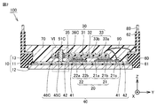
- FIG. 5 is a schematic cross-sectional view of a portion of the power semiconductor device according to the first embodiment of the first embodiment along the line II-II of FIG.
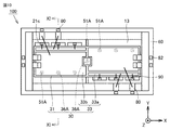
- FIG. 5 is a schematic plan view of a portion of the power semiconductor device of FIG. 1 in which semiconductor elements are arranged. It is a schematic plan view which shows the mode of the core material of the printed circuit board and the conductor layer which is lower side in the Z direction, among the semiconductor devices for electric power of FIG.
- FIG. 5 is a schematic enlarged cross-sectional view of a partial VI surrounded by a dotted line in FIG. 2 in the first example of the first embodiment. It is a schematic plan view which shows the aspect which viewed the whole of the semiconductor device for electric power of 2nd Example of Embodiment 1 in a plan view.
- FIG. 5 is a schematic cross-sectional view of a portion of the power semiconductor device of the second example of the first embodiment along the line VIII-VIII of FIG. FIG.
- FIG. 5 is a schematic enlarged cross-sectional view of a portion IX surrounded by a dotted line in FIG. 8 in the third example of the first embodiment.
- FIG. 5 is a schematic plan view showing a plan view of the entire power semiconductor device of the third example of the first embodiment.
- FIG. 5 is a schematic cross-sectional view of a portion of the power semiconductor device of the third example of the first embodiment along the XI-XI line of FIG.
- FIG. 5 is a schematic enlarged cross-sectional view of a portion XII surrounded by a dotted line in FIG. 11 in the third example of the first embodiment. It is the schematic sectional drawing of the part along the line II-II of FIG.
- FIG. 5 is a schematic cross-sectional view of a portion along line II-II of FIG. 1, showing a first step of the method for manufacturing a power semiconductor device according to a third example of the first embodiment.
- FIG. 5 is a schematic cross-sectional view of a portion along line II-II of FIG. 1, showing a second step of the method for manufacturing a power semiconductor device according to a third example of the first embodiment.
- It is schematic cross-sectional view of the part along the line II-II of FIG. 1, which shows the 2nd step of the manufacturing method of the electric power semiconductor device of 1st Example of Embodiment 1.
- FIG. 5 is a schematic cross-sectional view of a portion along line II-II of FIG. 1, showing a fourth step of the method for manufacturing a power semiconductor device according to a first embodiment of the first embodiment. It is a schematic plan view which shows the aspect which viewed the whole of the electric power semiconductor device of Embodiment 2 in a plan view.
- FIG. 5 is a schematic cross-sectional view of a portion of the power semiconductor device according to the second embodiment along the line XX-XX of FIG.
- FIG. 9 is a schematic plan view of a portion of the power semiconductor device of FIG. 19 in which semiconductor elements are arranged.
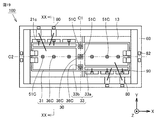
- 9 is a schematic plan view showing an aspect of a core material of a printed circuit board and a conductor layer on the lower side in the Z direction of the power semiconductor device of FIG. 9 is a schematic plan view showing an aspect of a core material of a printed circuit board and a conductor layer on the upper side in the Z direction of the power semiconductor device of FIG.
- It is a schematic plan view which shows the aspect which viewed the whole of the electric power semiconductor device of Embodiment 3 in a plan view.
- FIG. 6 is a schematic plan view of a portion of the power semiconductor device of FIG. 24 in which semiconductor elements are arranged.
- FIG. 5 is a schematic cross-sectional view of a portion of the power semiconductor device according to the fourth embodiment along the XXIX-XXIX line of FIG. 28.
- FIG. 5 is a schematic enlarged cross-sectional view of a portion XXX surrounded by a dotted line in FIG. 29 in the fourth embodiment.
- FIG. 5 is a schematic plan view of a portion of the power semiconductor device of FIG. 28 in which semiconductor elements are arranged. It is a schematic plan view which shows the mode of the core material of the printed circuit board, and the conductor layer which is lower side in the Z direction, among the semiconductor devices for electric power of FIG. 28.
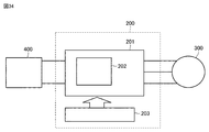
- FIG. 5 is a schematic cross-sectional view of a portion of the power semiconductor device according to the fourth embodiment along the line XXXIII-XXXIII of FIG. 28. It is a block diagram which shows the structure of the power conversion system to which the power conversion apparatus which concerns on Embodiment 5 is applied.
- FIG. 1 is a schematic plan view showing a plan view of the entire power semiconductor device of the first example of the first embodiment.
- FIG. 2 is a schematic cross-sectional view of a portion of the power semiconductor device of the first example of the first embodiment along the line II-II of FIG.
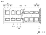
- FIG. 3 is a schematic plan view of a portion of the power semiconductor device of FIG. 1 in which a semiconductor element is arranged.
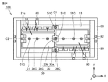
- FIG. 4 is a schematic plan view showing aspects of the core material of the printed circuit board and the conductor layer on the lower side in the Z direction of the power semiconductor device of FIG.
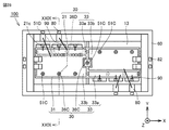
- FIG. 5 is a schematic plan view showing aspects of the core material of the printed circuit board and the conductor layer on the upper side in the Z direction of the power semiconductor device of FIG.
- FIG. 6 is a schematic enlarged cross-sectional view of a portion VI surrounded by a dotted line in FIG. 2 in the first example of the first embodiment.
- the lower side in the Z direction that is, the negative side in the Z direction
- the upper side in the Z direction that is, the positive side in the Z direction
- the positive side or the negative side in the X and Y directions extending in the horizontal direction in the figure will be simply referred to as the left side and the right side.
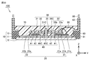
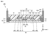
- the power semiconductor device 100 of the first example of the present embodiment includes an insulating substrate 10, a semiconductor chip 20, a printed circuit board 30, a conductive member 40, and a metal column portion. It mainly includes a 51C, a case 60, a sealing resin 70, an external electrode terminal 80, and a metal wire 90.
- the insulating substrate 10 is a flat plate-shaped member having, for example, a rectangular shape in a plan view.
- the insulating substrate 10 has an insulating layer 11, a fourth conductor layer 12, and a third conductor layer 13.
- the insulating layer 11 has a thickness of, for example, 0.125 mm.
- the insulating layer 11 is, for example, a resin insulating sheet.
- the insulating layer 11 is not limited to this, and may be formed of any ceramic material selected from the group consisting of, for example, AlN (aluminum nitride), alumina, and SiN (silicon nitride).
- the fourth conductor layer 12 is joined to the lower surface of the insulating layer 11.
- the fourth conductor layer 12 has, for example, a thickness of 2 mm.
- the third conductor layer 13 is arranged so as to be joined on the upper surface of the insulating layer 11, that is, on the surface of the insulating substrate 10 on the printed circuit board 30 side, which is the upper side.
- the third conductor layer 13 has, for example, a thickness of 0.5 mm.
- the fourth conductor layer 12 and the third conductor layer 13 are formed of, for example, copper.
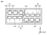
- the third conductor layer 13 has, for example, a rectangular shape in a plan view, and is arranged so as to be arranged at intervals in the X direction.
- two third conductor layers 13 are arranged at intervals in the X direction, but the number and mode of arrangement of the third conductor layers 13 are arbitrary.
- the third conductor layer 13 on the right side of the two may be a region on the left side thereof and may partially project to the left side from the other regions in the central portion of the insulating substrate 10.
- the third conductor layer 13 on the left side of the two may be a region on the right side thereof and may be partially recessed to the left side of the other regions in the central portion of the insulating substrate 10.
- the portion where the third conductor layer 13 on the right side protrudes is inserted into the portion where the third conductor layer 13 on the left side is recessed.
- the fourth conductor layer 12 may or may not have the same planar shape as the third conductor layer 13.
- the semiconductor chip 20 has, for example, an IGBT as a semiconductor element 21 and a diode 22 as another element different from the semiconductor element 21.
- These semiconductor chips 20, that is, the semiconductor element 21 and the diode 22 are bonded to one main surface of the insulating substrate 10, that is, the upper main surface. More specifically, the semiconductor element 21 and the diode 22 are bonded to the upper surface of the third conductor layer 13 at intervals in the X and Y directions.
- FWD is preferably used.
- the IGBT is mentioned as an example of the semiconductor element 21.
- a MOSFET Metal Oxide Semiconductor Field Effect Transistor
- FIG. 3 three semiconductor elements 21 and three diodes 22 are bonded in a row on each of the two third conductor layers 13 of the insulating substrate 10. That is, in FIG. 3, the semiconductor element 21 and the diode 22 are arranged in a pair, so-called 1in1.
- the number and arrangement of the semiconductor elements 21 and the diodes 22 are arbitrary.
- the semiconductor element 21 and the diode 22 may be arranged so as to form two pairs of 2in1 or six pairs of 6in1.
- a power semiconductor element serving as a converter, and a power semiconductor element serving as a brake may be mounted.
- the semiconductor element 21 is schematically shown so as to have one main electrode 21b and one signal electrode 21c on the chip main body 21a. That is, the semiconductor element 21 is formed with a main electrode 21b and a signal electrode 21c.
- the main electrode 21b is, for example, an emitter electrode
- the signal electrode 21c is, for example, a gate electrode.
- the diode 22 is schematically shown with one electrode 22b on the chip main body 22a.
- the semiconductor element 21 has a chip body 21a having, for example, a length of 8 mm, a width of 8 mm, and a thickness of 0.08 mm.
- the diode 22 has a chip body 22a having a length of 6 mm, a width of 8 mm, and a thickness of 0.08 mm.
- a gate electrode as a signal electrode 21c having a length of 1 mm and a width of 2 mm is formed.
- the number and arrangement of the main electrode 21b, the signal electrode 21c, and the electrode 22b of the diode 22 are arbitrary.
- the main electrode 21b, the signal electrode 21c, and the electrode 22b are all metal thin films formed of, for example, gold.
- a source electrode is arranged as a main electrode 21b and a gate electrode is arranged as a signal electrode 21c on the chip body.
- the printed circuit board 30 is a flat plate-shaped member having, for example, a rectangular shape in a plan view.
- the printed circuit board 30 is bonded to the semiconductor element 21 which is an IGBT and the diode 22 on the upper side thereof so as to face the diode 22.
- a solder layer 41 is arranged on the lower surface of the semiconductor element 21 and the diode 22, and a third conductive member 42, which is a solder layer, is arranged on the upper surface.
- the semiconductor element 21 and the diode 22 are joined to the third conductor layer 13 of the insulating substrate 10 on the lower side by the solder layer 41.
- the semiconductor element 21 and the diode 22 are joined by a third conductive member 42 to the first conductor layer 32 of the printed circuit board 30 on the upper side thereof, which will be described later.
- the main electrode 21b and the printed circuit board 30 are connected via a third conductive member 42.
- Both the solder layer 41 and the third conductive member 42 are included in the conductive member 40 described above.
- the thickness of the solder layer 41 is about 0.1 mm.
- the third conductive member 42 has a thickness of about 0.4 mm.
- the solder layer 41 and the third conductive member 42 are made of, for example, a Sn—Ag—Cu based solder material. However, here, not only Sn—Ag—Cu type solder but also other types of solder may be used for at least one of the solder layer 41 and the third conductive member 42. Alternatively, a conductive material other than solder may be used for the third conductive member 42. Further, instead of the solder layer 41, a conductive material other than solder may be used.
- a conductive adhesive in which a silver filler is dispersed in an epoxy resin, silver nanopowder or copper nanopowder in which nanoparticles are fired at a low temperature, or the like can be used. It may be used. Even when the conductive member is made of these materials, it has the same bonding effect as when the solder layer 41 and the third conductive member 42 are made of the solder layer 41.
- the insulating substrate 10 is bonded to the lower side of the semiconductor chip 20. Therefore, the insulating substrate 10 enables electrical connection with an electrode (not shown) on the lower surface of the semiconductor chip 20. A more detailed description of the conductive member 40 will be described later.
- the maximum area of the rectangle in the plan view of the printed circuit board 30 may be smaller than the maximum area of the rectangle in the plan view of the insulating substrate 10.
- the maximum flat area may be larger for the printed circuit board 30 than for the insulating substrate 10, or both may be substantially the same.
- the printed circuit board 30 is arranged so that the center point of the rectangular planar shape thereof substantially coincides with the central point of the rectangular planar shape of the insulating substrate 10.
- the center point of the planar shape of the printed circuit board 30 and the center point of the planar shape of the insulating substrate 10 do not have to coincide with each other.
- the distance between the two center points in the X direction may be 5% or less or more than 5% of the maximum dimension of the printed circuit board 30 in the X direction.
- the Y direction is the same as the X direction.
- the center point of the insulating substrate 10 means a place where rectangular diagonal lines intersect in a plan view of the insulating substrate 10.
- the center point of the insulating substrate 10 means the position of the center of gravity thereof.
- the printed circuit board 30 has a core material 31, a first conductor layer 32, and a second conductor layer 33.
- the first conductor layer 32 is formed on the semiconductor element 21 side of the core material 31, that is, on the lower first main surface of the core material 31 close to the semiconductor chip 20.
- the second conductor layer 33 is formed on the side opposite to the first main surface of the core material 31, that is, on the upper second main surface of the core material 31 far from the semiconductor chip 20.
- the first conductor layer 32 is joined to the semiconductor element 21 and the diode 22 via the third conductive member 42. Therefore, the printed circuit board 30 is arranged along the main surface of the semiconductor chip 20 so as to face the upper side of the semiconductor element 21 mounted on the insulating substrate 10.
- the core material 31 has, for example, a thickness of 0.5 mm.
- the core material 31 is, for example, an insulating material whose material is called FR-4 (Flame Retardant Type 4).
- Both the first conductor layer 32 and the second conductor layer 33 have a thickness of, for example, 0.4 mm, and are formed of, for example, copper.
- two first conductor layers 32 are arranged at intervals in the X direction, for example, having a relatively large flat area. These two first conductor layers 32 are line-symmetrical with each other with respect to a center line (not shown) extending in the vertical direction of the figure, that is, in the depth direction, at the center in the X direction.
- the one on the left side of FIG. 4 has the rightmost side, that is, the outer edge, recessed on the left side of FIG. 4 near the center of the printed circuit board 30.
- the one on the right side of FIG. 4 has the leftmost side, that is, the outer edge, recessed on the right side of FIG. 4 near the center of the printed circuit board 30.
- the recessed portions of each of these two first conductor layers 32 surround the central portion of the printed circuit board 30 in a plan view while facing each other in the X direction.
- Each side of these two first conductor layers 32 is formed in a rectangular shape except for the above-mentioned recessed portion.
- the upper and lower outer edges of the two first conductor layers 32 in FIG. 4 may be formed so as to overlap the outer edges of the printed circuit board 30.
- the upper and lower outer edges of the two first conductor layers 32 in FIG. 4 may be formed inside the printed circuit board 30 so as not to overlap the outer edges of the printed circuit board 30.
- One rectangular or square pattern of the first conductor layer 32 is formed in the central portion of the printed circuit board 30 in a plan view.
- the central first conductor layer 32 has a smaller flat area than the two first conductor layers 32 described above.
- the first conductor layer 32 in the central portion is formed as the same layer as each of the above two first conductor layers 32.
- planar shapes and arrangements of the three first conductor layers 32 shown in FIG. 4 are line-symmetrical with respect to the central line passing through the central portion in the X direction of FIG. 4, for example. Further, the planar shapes of the three first conductor layers 32 are line-symmetrical with respect to the central line passing through the central portion in the Y direction of FIG. 4 in the lateral direction. Further, the planar shapes and arrangements of the three first conductor layers 32 are point-symmetrical with respect to the central point in FIG. 4, for example.
- two second conductor layers 33 are formed, for example, at intervals in the X direction. However, each of these two is further divided into two at a distance from each other in the Y direction. That is, in the left half region of FIG. 5, a non-bonding pad 33b having a relatively large flat area and a bonding pad 33a are arranged as the second conductor layer 33. That is, the second conductor layer 33 has a bonding pad 33a as a part thereof.
- the bonding pad 33a is arranged on the upper side of the non-bonding pad 33b in the left region of FIG. 5, that is, on the inner side in the depth direction.
- the bonding pad 33a has a narrower width in the Y direction than the non-bonding pad 33b.
- the bonding pad 33a has a rectangular shape extending in the X direction.
- a non-bonding pad 33b having a relatively large flat area and a bonding pad 33a are arranged as the second conductor layer 33. That is, the second conductor layer 33 has a bonding pad 33a as a part thereof.
- the bonding pad 33a is arranged on the lower side of the non-bonding pad 33b in the right region of FIG. 5, that is, on the front side in the depth direction.
- the bonding pad 33a has a narrower width in the Y direction than the non-bonding pad 33b.
- the bonding pad 33a has a rectangular shape extending in the X direction.
- the two non-bonding pads 33b and the bonding pads 33a constituting the second conductor layer 33 have a center line in the X direction extending in the vertical direction, that is, in the depth direction of the drawing, with respect to a center line (not shown). They are line symmetric with each other.
- the rightmost side, that is, the outer edge of these two non-bonding pads 33b is recessed on the left side of FIG. 5 near the center of the printed circuit board 30.
- the one on the right side in FIG. 5 has the leftmost side, that is, the outer edge, recessed on the right side in FIG. 5 near the center of the printed circuit board 30.
- the recessed portions of each of these two non-bonding pads 33b surround the central portion of the printed circuit board 30 in a plan view while facing each other in the X direction.
- Each side of these two non-bonding pads 33b is formed in a rectangular shape except for the above-mentioned recessed portion.
- the uppermost and lowermost outer edges of the second conductor layer 33 in FIG. 5 may be formed inside the printed circuit board 30 so as not to overlap the outer edges of the printed circuit board 30.
- the upper and lower outer edges of the second conductor layer 33 in FIG. 5 may be formed so as to overlap the outer edges of the printed circuit board 30.
- One rectangular or square pattern of the second conductor layer 33 is formed in the central portion of the printed circuit board 30 in a plan view.
- the second conductor layer 33 in the central portion is a non-bonding pad 33b having a smaller flat area than the non-bonding pad 33b of the two second conductor layers 33 described above.
- the central non-bonding pad 33b is formed as the same layer as each of the above two large non-bonding pads 33b and the two bonding pads 33a.
- planar shapes and arrangements of the second conductor layers 33 divided into a total of five shown in FIG. 5 are line-symmetrical with respect to the central line passing through the central portion in the X direction of FIG. 5, for example. is there. Further, the planar shapes of the five second conductor layers 33 are line-symmetrical with respect to the central line passing through the central portion in the Y direction of FIG. 5 in the lateral direction. Further, the planar shapes and arrangements of the five second conductor layers 33 are point-symmetrical with respect to the central point in FIG. 5, for example.
- At least a part of the emitter electrode and the like, which is the main electrode 21b to which the third conductive member 42 of the semiconductor element 21 is attached, is arranged at a position where the bonding pad 33a and the bonding pad 33a are planarly overlapped with each other. Is preferable.
- the entire main electrode 21b to which the third conductive member 42 of the semiconductor element 21 is attached may be arranged at a position where it overlaps with the bonding pad 33a in a plane.
- connection portion between the semiconductor chip 20 and the printed circuit board 30 has the following features.
- the signal electrode 21c such as the gate electrode of the IGBT and the bonding pad 33a are electrically connected by a metal wire 90.
- At least a part of the joining portion of the metal wire 90 joined to the bonding pad 33a connects the main electrode 21b of the semiconductor element 21 and the first conductor layer 32. It is arranged at a position facing the third conductive member 42 in the Z direction. That is, at least a part of the position where the metal wire 90 is bonded on the bonding pad 33a is arranged at a position where it planely overlaps with the third conductive member 42 of the semiconductor element 21.
- the entire position where the metal wire 90 is bonded on the bonding pad 33a may be arranged at a position where the entire position where the metal wire 90 is bonded overlaps the third conductive member 42 of the semiconductor element 21 in a plane.
- the position of the joint portion of the metal wire 90 is not limited to the position facing the third conductive member 42 as long as it is on the bonding pad 33a, and is arbitrary.
- the printed circuit board 30 is partially missing the core material 31, the first conductor layer 32, and the second conductor layer 33.
- This partially missing portion is the penetration portion 36C.
- the penetrating portion 36C penetrates the core material 31 from the first main surface to the second main surface in the Z direction, and further overlaps the core material 31 in a plane with the first conductor layer 32 and the second conductor layer. It penetrates 33 in the Z direction. That is, the penetrating portion 36C penetrates the second conductor layer 33 from the uppermost surface to the lowermost surface of the first conductor layer 32 so as to extend along the Z direction.
- a conductor layer may be formed on the inner wall surface of the penetrating portion 36C. More specifically, a conductor layer joint portion 35 that conducts the first conductor layer 32 and the second conductor layer 33 may be formed on the inner wall surface of the penetrating portion 36C. That is, in FIG. 2, the first conductor layer 32 and the second conductor layer 33 are conducted by the conductor layer joint portion 35 on the inner wall surface of the penetrating portion 36C.
- the conductor layer joining portion 35 is formed of a conductor thin film such as copper that electrically and mechanically joins the first conductor layer 32 and the second conductor layer 33 on the inner wall surface of the penetrating portion 36C.
- the conductor layer joint portion 35 is, for example, a copper plating film formed on the inner wall surface of the penetration portion 36C independently of the first conductor layer 32 and the second conductor layer 33.
- the conductor layer joint portion 35 is not formed in the penetrating portion 36C, and the surface of the metal column portion 51C may come into direct contact with the inner wall surface of the penetrating portion 36C.
- the metal pillar portion 51C is inserted so as to extend in the penetrating portion 36C along the Z direction.
- the metal column portion 51C is connected to the printed circuit board 30 by the first conductive member 46C. That is, both the first conductive member 46C as the conductive member 40 and the metal column portion 51C are arranged in the penetrating portion 36C. In other words, the inside of the penetrating portion 36C is filled with the metal column portion 51C and the first conductive member 46C.
- the first conductive member 46C is made of, for example, solder, and fills a region from the side surface of the metal column portion 51C to the inner wall surface of the penetrating portion 36C.
- the metal pillar portion 51C and the penetrating portion 36C in other words, the metal pillar portion 51C and the first conductor layer 32 and the second conductor layer 33 of the printed circuit board 30 are electrically connected by the first conductive member 46. Will be done.
- the metal column portion 51C penetrates through the penetrating portion 36C from the uppermost surface of the third conductor layer 13 as one main surface of the insulating substrate 10 and exceeds the uppermost surface of the penetrating portion 36C on the opposite side of the insulating substrate 10. It extends to the side opposite to the insulating substrate 10 of the printed circuit board 30. That is, the metal column portion 51C extends along the Z direction to the outside, that is, the upper side of the penetration portion 36C.
- the side of the printed circuit board 30 opposite to the insulating substrate 10 is the upper side of the second conductor layer 33.
- the metal column portion 51C penetrates the core material 31, the first conductor layer 32, and the second conductor layer 33 of the printed circuit board 30 so as to extend in the Z direction.
- the metal column portion 51C is preferably formed of copper in consideration of electrical conductivity, thermal conductivity, and bondability with solder.
- the metal column portion 51C also has a cylindrical shape.
- the penetrating portion 36C and the metal column portion 51C may have a polygonal column shape.
- the metal column portion 51C has a cylindrical shape.
- the metal pillar portion 51C may have a portion made of a metal material extending in a tubular shape and a hollow central portion in a plan view.
- the metal pillar portion 51C may be entirely made of a metal material, and the entire metal pillar portion 51C including the central portion in a plan view may be filled with the metal material.
- a conductor layer joint 35 is formed on the inner wall surface of the penetrating portion 36C, and the conductor layer joint 35 is sandwiched between the first conductive member 46C and the penetrating portion 36C.
- the metal column portion 51C is connected to the printed circuit board 30 in the penetrating portion 36C.
- the metal column portion 51C is joined or in contact with the printed circuit board 30 in the through portion 36C.
- the lower side of the metal column portion 51C reaches the uppermost surface of the insulating substrate 10. That is, the lowermost portion of the metal column portion 51C contacts the uppermost surface of the third conductor layer 13.
- the metal column portion 51C and the uppermost surface of the insulating substrate 10 are joined by a second conductive member 45C.
- the second conductive member 45C as the conductive member 40 is also made of, for example, solder like the others.
- a plurality of penetrating portions 36C and metal pillar portions 51C inside the penetrating portion 36C are arranged. It is preferable that the plurality of metal column portions 51C are arranged at positions that are point-symmetrical with respect to the center of the insulating substrate 10 in a plan view. Specifically, the metal column portion 51C and the penetrating portion 36C are provided at the Y-direction ends of the two large non-bonding pads 33b, which are opposite to the bonding pad 33a adjacent to them in the Y direction. Three are formed at intervals in the X direction.
- the metal column portion 51C and the penetrating portion 36C are formed so as to include one in the small non-bonding pad 33b at the center in the plan view, for example, the center point in the plan view of the printed circuit board 30. That is, one of the plurality of metal column portions 51C is arranged at the center of the printed circuit board 30 in a plan view.
- the penetrating portion 36C, the metal column portion 51C, the diode 22, and the semiconductor element 21 are arranged in this order with a gap from each other.
- the penetrating portion 36C, the metal column portion 51C, the diode 22, and the semiconductor element 21 are arranged in this order from the negative side to the positive side in the Y direction.
- the semiconductor element 21, the diode 22, the penetrating portion 36C, and the metal column portion 51C are arranged in this order from the negative side to the positive side in the Y direction.
- each of the plurality of metal column portions 51C and the penetrating portion 36C is arranged at positions that are point-symmetrical with respect to the center point of the insulating substrate 10 in a plan view. Further, it is preferable that these are arranged at positions that are point-symmetrical with respect to the center point of the printed circuit board 30 in a plan view.
- the other plurality of metal column portions 51C except for one metal column portion 51C are arranged at the center of the printed circuit board 30, that is, at positions symmetrical with respect to, for example, the center point. preferable.
- the current capacity can be calculated by the product of the cross-sectional area and the current density intersecting the extending direction of the metal column portion 51C. For example, consider the case where a metal column portion 51C having a circular cross section with a diameter of 2.0 mm is made of copper. In this case, the current capacity per metal column portion 51C is about 200A.
- the metal column portion 51C has a diameter of 2.0 mm, three or more may be arranged.
- the three metal column portions 51C connected to the first conductor layer 32 and the second conductor layer 33 having a large flat area in FIG. 4 correspond to the U phase, the V phase, and the W phase, respectively.
- the main electrode 21b of the semiconductor element 21 and the surface electrode (not shown) of the diode 22 are connected by a conductive member 40. If the main electrode 21b such as the emitter electrode and the surface electrode (not shown) of the diode 22 are connected by the metal column portion 51C, a large current flows through the metal column portion 51C. Therefore, it is necessary to disperse the current by arranging a plurality of metal column portions 51C. When arranging a plurality of metal column portions 51C, it is necessary to form a very large number of through portions 36C on the printed circuit board 30 at a narrow pitch. However, it is difficult to process a large number of penetrating portions 36C at such a narrow pitch, and it may not be possible to form the required number. Therefore, by connecting the main electrode 21b and the surface electrode of the diode 22 with the conductive member 40 as described above, the volume required for passing a large current can be easily supplied by the conductive member 40.
- the main electrode 21b and the surface electrode of the diode 22 are arranged so as to overlap the printed circuit board 30 in a plane and be covered by the printed circuit board 30 from above.
- the signal electrode 21c is arranged so as not to be covered with the printed circuit board 30.
- the distance between the signal electrode 21c and the end portion, that is, the outer edge of the printed circuit board 30 is avoided in order to avoid interference between the bonding tool and the printed circuit board 30. It is necessary to provide 1 mm or more.
- the metal column portion 51C functions as a conductor that electrically connects the third conductor layer 13 and the first conductor layer 32 and the second conductor layer 33 of the printed circuit board 30 facing the third conductor layer 13. That is, the third conductor layer 13 of the insulating substrate 10 and the first conductor layer 32 and the second conductor layer 33 of the printed circuit board 30 facing the third conductor layer 13 form the second conductive member 45, the metal column portion 51C, and the metal pillar portion 51C. It is electrically connected via the first conductive member 46 (as well as the conductor layer joint 35).
- the metal column portion 51C is controlled so that the gap (distance in the Z direction) between the third conductor layer 13 and the first conductor layer 32 becomes a constant value.
- the dimensions of the plurality of metal column portions 51C in the Z direction are almost the same.
- the distance between the two is preferably 0.3 mm or more.
- the length H2 extending upward in the Z direction of the metal column portion 51C is larger than the length H1 extending downward in the Z direction on the outside of the printed circuit board 30. ..
- the length H1 is 0.5 mm or even shorter. H1 may be slightly increased from 0.5 mm.
- the length H2 is preferably at least 0.5 mm or more.
- the length H2 is, for example, about 1 mm or more and 3 mm or less, and more preferably 1.5 mm or more and 2 mm or less.
- the case 60 is arranged so as to surround the outer edge portion of the insulating substrate 10 in a plan view and to accommodate the semiconductor element 21, the diode 22, the printed circuit board 30, and the like on the outer edge portion. That is, a container-shaped member is formed by the insulating substrate 10 and the case 60, the semiconductor element 21, the diode 22, the printed circuit board 30, and the like are housed in the container-shaped member, and the inside of the container-shaped member is made of the sealing resin 70. It is in a filled mode.
- the sealing resin 70 is made of, for example, an epoxy resin.
- a part of the insulating substrate 10, specifically, for example, the lower region of the fourth conductor layer 12 may be exposed outward from the container-shaped member.
- the case 60 is adhered to the region of the main surface of the insulating substrate 10 adjacent to the end faces of the insulating layer 11 and the fourth conductor layer 12 and the end faces of the fourth conductor layer 12 by a silicone adhesive (not shown).
- the case 60 is, for example, a member containing PPS (polyphenylene sulfide) as a main component.
- PPS polyphenylene sulfide
- the case 60 may be formed by using LCP (liquid crystal polymer) having higher heat resistance than PPS.
- the case 60 has a region having a relatively wide width in the X direction (and a Y direction not shown) below the case 60 and a region having a relatively narrow width in the X direction (and the Y direction) above the case 60. have.
- the case 60 has a groove extending horizontally from the case inner surface 61 of the wide region, bending from the wide region, and extending in the Z direction along the case inner surface 62 of the narrow region. It is formed.
- the external electrode terminal 80 and the external main electrode terminal 82 are arranged so as to fit in the groove.
- the external electrode terminal 80 is electrically connected to the bonding pad 33a of the printed circuit board 30 via the metal wire 90. Therefore, the external electrode terminal 80 is electrically connected to the signal electrode 21c.
- the external main electrode terminal 82 is electrically connected to the bonding pad 33a of the printed circuit board 30 via the metal wire 90. Therefore, the external main electrode terminal 82 is electrically connected to the signal electrode 21c. Further, the external electrode terminal 80 is electrically connected to the main electrode 21b and the signal electrode 21c via a metal wire 90.
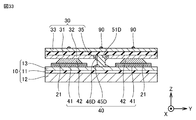
- FIG. 7 is a schematic plan view showing a plan view of the entire power semiconductor device of the second example of the first embodiment.
- FIG. 8 is a schematic cross-sectional view of a portion of the power semiconductor device of the second example of the first embodiment along the line VIII-VIII of FIG.
- FIG. 9 is a schematic enlarged cross-sectional view of a portion IX surrounded by a dotted line in FIG. 8 in the third example of the first embodiment.
- the power semiconductor device 100 of the second example of the present embodiment has basically the same configuration as the power semiconductor device 100 of the first example of the present embodiment. have. Therefore, the same components are designated by the same reference numerals, and the description of matters common to the first example will not be repeated. Further, even if the reference numerals are different, the content of not repeating the following description is basically the same as that of the first example.
- the portion where the core material 31, the first conductor layer 32, and the second conductor layer 33 constituting the printed circuit board 30 are partially missing is the penetration portion 36B. ..
- the penetrating portion 36B has the same shape, mode, position, and the like as the penetrating portion 36C.
- a metal pillar portion 51B is inserted into the penetrating portion 36B instead of the metal pillar portion 51C.
- the metal column portion 51B is connected to the printed circuit board 30 by a first conductive member 46B in the penetrating portion 36B.
- the lowermost portion of the metal column portion 51B is connected to the third conductor layer 13 of the insulating substrate 10 by the second conductive member 45B.
- the symbols are different, the materials, arrangement, and the like of the first conductive member 46B and the second conductive member 45B are the same as those of the first conductive member 46C and the second conductive member 45C.
- the metal pillar portion 51B is inserted so as to extend in the penetrating portion 36B along the Z direction, similarly to the metal pillar portion 51C of the first example.
- the metal column portion 51B extends upward along the Z direction from the inside of the penetrating portion 36B, beyond the uppermost surface of the second conductor layer 33 of the printed circuit board 30, to the outside of the penetrating portion 36B.
- the shape, material, etc. of the metal pillar portion 51B are basically the same as those of the metal pillar portion 51C.
- the metal pillar portion 51B has a head portion 51B1 and a columnar portion 51B2.
- the head portion 51B1 is a portion of the metal column portion 51B that is arranged outside the penetrating portion 36B and extends in the XY directions along one main surface of the insulating substrate 10.
- the head portion 51B1 is a region of the metal column portion 51B extending above the second conductor layer 33 in FIG. 9 along the left-right direction, that is, the Y direction in the figure.
- the head portion 51B1 is a region in which the columnar portion 51B2 extending upward in the Z direction extends beyond the third main surface of the printed circuit board 30 in the Z direction and is arranged outside the penetrating portion 36B.
- the columnar portion 51B2 is a region of the metal pillar portion 51B other than the head portion 51B1.
- the columnar portion 51B2 is a region extending from (the lowermost surface) of the head 51B1 along the penetrating portion 36B so as to include an internal region of the penetrating portion 36B.
- the columnar portion 51B2 has, for example, a cylindrical shape, but is not limited to this.
- the columnar portion 51B may have a polygonal prism shape.
- the columnar portion 51B2 may have a portion made of a metal material extending in a tubular shape and a hollow central portion in a plan view.
- the columnar portion 51B2 may be entirely made of a metal material, and the entire columnar portion 51B2 including the central portion in a plan view may be filled with the metal material. Therefore, the head 51B1 is arranged outside the penetrating portion 36B so as to be connected to one end (uppermost portion) of the columnar portion 51B2 in the extending direction.
- the metal column portion 51B is different from the metal column portion 51C in the cross-sectional shape of the uppermost portion in the Z direction, particularly the upper region of the third conductor layer 13 of the insulating substrate 10.
- FIG. 10 is a schematic plan view showing a plan view of the entire power semiconductor device of the third example of the first embodiment.
- FIG. 11 is a schematic cross-sectional view of a portion of the power semiconductor device of the third example of the first embodiment along the XI-XI line of FIG.
- FIG. 12 is a schematic enlarged cross-sectional view of a portion XII surrounded by a dotted line in FIG. 11 in the third example of the first embodiment.
- the power semiconductor device 100 of the third example of the present embodiment has basically the same configuration as the power semiconductor device 100 of the first example of the present embodiment. have. Therefore, the same components are designated by the same reference numerals, and the description of matters common to the first example will not be repeated. Further, even if the reference numerals are different, the content of not repeating the following description is basically the same as that of the first example.
- the portion of the printed circuit board 30 in which the first conductor layer 32 is partially missing is the missing portion 36A.
- the missing portion 36A is formed at the same position as the penetrating portions 36B and 36C. However, the missing portion 36A is formed so as to expose the first main surface of the core material 31 directly below the missing portion 36A by penetrating the first conductor layer 32 in the formed region.
- the missing portion 36A is not formed so as to miss the core material 31 and the second conductor layer 33.
- the missing portion 36A penetrates only a part in the Z direction connecting the first main surface and the second main surface of the printed circuit board 30. Therefore, the missing portion 36A does not penetrate the printed circuit board 30.
- the penetrating portions 36B and 36C as the missing portions penetrate all of the first conductor layer 32, the core material 31, and the second conductor layer 33 by penetrating the entire printed circuit board 30 in the Z direction.
- the third example is different from the first and second examples.
- a metal pillar portion 51A is inserted in the missing portion 36A instead of the metal pillar portion 51C.
- the metal pillar portion 51A is connected to the printed circuit board 30 by a first conductive member 46A in the missing portion 36A.
- the lowermost portion of the metal column portion 51A is connected to the third conductor layer 13 of the insulating substrate 10 by the second conductive member 45A.
- the materials of the first conductive member 46A and the second conductive member 45A are the same as those of the first conductive member 46C and the second conductive member 45C.
- the metal pillar portion 51A is inserted so as to extend in the missing portion 36A along the Z direction.
- the metal column portion 51A extends downward along the Z direction from the inside of the missing portion 36A to the uppermost surface of the third conductor layer 13 of the insulating substrate 10.
- the material of the metal pillar portion 51A is basically the same as that of the metal pillar portion 51C.
- the metal pillar portion 51A may have a portion made of a metal material extending in a tubular shape and a hollow central portion in a plan view.
- the metal pillar portion 51A may be entirely made of a metal material, and the entire metal pillar portion 51A including the central portion in a plan view may be filled with the metal material.
- the metal pillar portion 51A does not penetrate the printed circuit board 30.
- the metal column portion 51A is different from the metal column portion 51B and the metal column portion 51C.
- FIGS. 13 to 18 are all shown as schematic cross-sectional views of the portion along the line II-II of FIG. 1 as in FIG. 2.
- FIGS. 13 to 15 are reversed in the Z direction, that is, upside down.
- the process may be performed without reversing the Z direction as in FIGS. 16 to 18.
- FIG. 13 is a schematic cross-sectional view of a portion along the line II-II of FIG. 1, showing the first step of the method of manufacturing the power semiconductor device of the first example of the first embodiment.
- the core material 31, the first conductor layer 32 formed on the first main surface of the core material 31, and the core material are used.
- a printed circuit board 30 including a second conductor layer 33 formed on a second main surface opposite to the first main surface of 31 is prepared.
- a missing portion is formed in which the first conductor layer 32 is partially missing.
- FIG. 13 is a schematic cross-sectional view of a portion along the line II-II of FIG. 1, showing the first step of the method of manufacturing the power semiconductor device of the first example of the first embodiment.
- the missing portion penetrates not only the first conductor layer 32 but also the entire direction connecting the first main surface and the second main surface of the printed circuit board 30.
- the printed circuit board 30 in which the penetrating portion 36C penetrating all of the first conductor layer 32, the core material 31, and the second conductor layer 33 is formed is prepared.
- the metal pillar portion 51C is inserted into the penetrating portion 36C.
- the positions of the printed circuit board 30 and the metal pillar portion 51C are determined by fixing them with a jig. That is, the positional relationship between the penetrating portion 36C and the metal pillar portion 51C in the X and Y directions and the position of the metal pillar portion 51C in the Z direction are determined by fixing a jig (not shown).
- the metal pillar portion 51C that is inserted through the penetration portion 36C and extends to the outside of the penetration portion 36C is fixed to the printed circuit board 30.
- the inside of the penetrating portion 36C that is, the space portion surrounded by the inner wall surface of the penetrating portion 36B (or the surface of the conductor layer joint portion 35 whose inner wall surface is plated with copper, for example) and the metal column portion 51C
- the molten solder for forming the conductive member 46C of 1 is supplied.
- the supplied molten solder is instantly solidified by natural air cooling. As a result, the molten solder becomes the first conductive member 46C.
- the metal column portion 51C is joined into the penetrating portion 36C by the first conductive member 46C.
- the molten solder for forming the first conductive member 46C is supplied as heated thread-like solder by a soldering iron, a soldering robot, or the like.
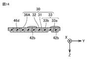
- FIG. 14 is a schematic cross-sectional view of a portion along the line II-II of FIG. 1, showing the first step of the method for manufacturing the power semiconductor device of the third example of the first embodiment.
- FIG. 15 is a schematic cross-sectional view of a portion along line II-II of FIG. 1, showing a second step of the method for manufacturing a power semiconductor device according to a third example of the first embodiment.
- the core material 31, the first conductor layer 32, and the second conductor layer 33 are the same as in FIG.
- the printed circuit board 30 including the above is prepared.
- a missing portion 36A in which the first conductor layer 32 is partially missing is formed.
- the missing portion penetrates only the first conductor layer 32 so as to be partially missing.
- the penetrating portions 36B, 36C or the missing portion 36A may be formed after purchasing the printed circuit board 30.
- the printed circuit board 30 on which the through portion 36B, 36C or the missing portion 36A is already formed may be purchased.
- a molten solder 46d for forming the first conductive member 46A is supplied into the missing portion 36A.
- the thread-like solder is supplied as heated by a soldering iron or a soldering robot.
- the metal column portion 51A is inserted into the missing portion 36A and extends to the outside of the missing portion 36A as shown in FIG. 15 before the solder 46d is supplied. It is preferable that the solder 46d is supplied after the arrangement. In this way, as shown in FIG. 15, the inserted metal column portion 51A is joined to the missing portion 36A by the first conductive member 46A.
- paste-like solder may be injected instead of molten solder.
- the paste-like solder 46d is injected into the missing portion 36A.
- a reflow step is performed on the printed circuit board 30 described above.
- the paste-like solder 46d solidifies as the first conductive member 46A. Therefore, the metal column portion 51A is fixed and joined to the missing portion 36A via the first conductive member 46A so as to extend from the inside of the missing portion 36A to the outside thereof.
- bump-shaped solder 42b is formed on the surface of the first conductor layer 32 that should be the lowermost surface facing the main electrode 21b and the diode 22.
- the bump-shaped solder 42b may be supplied with paste-like solder by printing or a dispenser on the surface to be the lowermost surface of the first conductor layer 32.
- the bump-shaped solder 42b may be supplied as solid solder on the surface to be the lowermost surface of the first conductor layer 32.
- the supplied solder may be formed as a solid bump-shaped solder 42b by a reflow step to the printed circuit board 30.
- the step of forming the bump-shaped solder 42b may be performed before the step of joining the metal column portion to the missing portion or the penetrating portion.
- FIG. 16 is a schematic cross-sectional view of a portion along the line II-II of FIG. 1, showing the second step of the method for manufacturing the power semiconductor device of the first example of the first embodiment.
- the insulating substrate 10 includes an insulating layer 11, a fourth conductor layer 12 formed on a lower surface thereof, and a third conductor layer 13 formed on an upper surface thereof. Is prepared.
- a semiconductor element 21 in which, for example, a signal electrode 21c as a gate electrode is formed is bonded onto one main surface of the insulating substrate 10, that is, on the third conductor layer 13. In the step of preparing the insulating substrate 10, the semiconductor element 21 may be bonded after purchasing the insulating substrate 10.
- the insulating substrate 10 to which the semiconductor element 21 is already bonded may be purchased.
- a diode 22 is bonded to the third conductor layer 13 at intervals from the semiconductor element 21.
- the semiconductor element 21 as the semiconductor chip 20 and the diode 22 are bonded to the third conductor layer 13 of the insulating substrate 10 by the solder layer 41 as the conductive member 40. That is, in a state where the semiconductor element 21 and the diode 22 are mounted on the third conductor layer 13 with the paste-like solder as the solder layer 41 sandwiched between them, the semiconductor chip 20 is formed by the solidified solder layer 41 after the reflow process is performed once. Is fixed and joined.
- a paste-like solder 42d for forming a third conductive member 42 (see FIG. 2) is supplied on the main electrode 21b of the semiconductor element 21 by printing or a dispenser or the like. Ru.
- a paste-like solder 45d for forming the second conductive member 45C is supplied on the third conductor layer 13 of the insulating substrate 10.
- the process of FIG. 16 may be performed after the process of FIGS. 13 to 15, but may be performed before the process of FIGS. 13 to 15.
- FIG. 17 is a schematic cross-sectional view of a portion along line II-II of FIG. 1, showing a third step of the method for manufacturing a semiconductor device for electric power according to the first example of the first embodiment.
- the printed circuit board 30 inverted upside down with respect to FIGS. 13 to 15 is arranged so as to face the upper side of the insulating substrate 10.
- the steps of FIGS. 13 to 15 are performed without being inverted as described above, the printed circuit board 30 is not inverted in FIG. 17 and is processed as it is.
- the paste-like solder 45d adheres to the lowermost portion of the metal column portion 51C.
- the bump-shaped solder 42b and the paste-shaped solder 42d adhere to each other.
- the paste-like solder 42d on the semiconductor chip 20 adheres to the lowermost portion of the first conductor layer 32.
- the reflow process is performed in this state. As a result, the bump-shaped solder 42b and the paste-shaped solder 42d are fixed as the third conductive member 42, and the semiconductor chip 20 and the first conductor layer 32 are joined.
- the paste-like solder 45d is fixed as the second conductive member 45C, and the metal column portion 51C and the third conductor layer 13 are joined via the second conductive member 45C. That is, the metal column portion 51C and the insulating substrate 10 are joined by the second conductive member 45C.
- the metal column portion 51C penetrates through the penetrating portion 36C from above the third conductor layer 13 which is one main surface of the insulating substrate 10, and is on the opposite side of the penetrating portion 36C from the insulating substrate 10. It is arranged so as to extend to a certain upper side.
- both the bump-shaped solder 42b and the paste-shaped solder 42d are formed in order to form the third conductive member 42 is as follows.
- the deformable paste-like solder 42d can absorb variations in the thickness of the already solidified bump-like solder 42b in the Z direction.
- the third conductive member 42 is formed to have a more uniform thickness, and the bonding between the semiconductor chip 20 and the printed circuit board 30 can be made of higher quality.
- both the bump-shaped solder 42b and the paste-shaped solder 42d are formed.
- the bump-shaped solder 42b may be formed on the insulating substrate 10 and the paste-shaped solder 42d may be formed on the printed circuit board 30.
- FIG. 18 is a schematic cross-sectional view of a portion along line II-II of FIG. 1, showing a fourth step of the method for manufacturing a semiconductor device for electric power according to the first example of the first embodiment.
- the case 60 is arranged on the insulating substrate 10. That is, the groove formed in the lower part of the case 60 is in a mode in which the edges of the insulating substrate 10, particularly the insulating layer 11 and the fourth conductor layer 12, enter and come into contact with each other.
- the case 60 and the insulating substrate 10 are fixed by a thermosetting adhesive (not shown).
- the signal electrode 21c and the bonding pad 33a are connected by a metal wire 90. This connection is made by a generally known wire bonding process.
- the bonding pad 33a and the external electrode terminal 80 are wired by the metal wire 90.
- the region in which the semiconductor element 21, the metal column 51C, the printed circuit board 30, and the like in the container-shaped member composed of the case 60 and the insulating substrate 10 are housed is filled with the thermosetting sealing resin 70. Will be done.
- the sealing resin 70 is heat-cured. By this heat curing, the sealing resin 70 seals the inside of the container-shaped member. As a result, the power semiconductor device 100 according to the aspect shown in FIG. 2 is formed.
- the power semiconductor device 100 includes an insulating substrate 10, a semiconductor element 21, and a printed circuit board 30.
- the semiconductor element 21 is bonded to one main surface of the insulating substrate 10.
- the printed circuit board 30 is joined so as to face the semiconductor element 21.
- a main electrode 21b and a signal electrode 21c are formed on the semiconductor element 21.
- the printed circuit board 30 has a core material 31, a first conductor layer 32 formed on the first main surface of the core material 31 on the semiconductor element 21 side, and a first surface of the core material 31 opposite to the first main surface.
- the second conductor layer 33 has a bonding pad 33a.
- the printed circuit board 30 is formed with missing portions 36A, 36B, and 36C in which the first conductor layer 32 is partially missing.
- Metal column portions 51A, 51B, 51C are further provided, which are inserted through the missing portions 36A, 36B, 36C to reach the insulating substrate 10 and are connected to the printed circuit board 30 by the first conductive members 46A, 46B, 46C.
- the signal electrode 21c and the bonding pad 33a are connected by a metal wire 90.
- the metal column portions 51A, 51B, 51C and the insulating substrate 10 are joined by the second conductive members 45A, 45B, 45C.
- an insulating substrate 10 in which a semiconductor element 21 on which a signal electrode 21c is formed is bonded on one main surface is prepared.
- a printed circuit board 30 is prepared in which the missing portions 36A, 36B, and 36C in which the first conductor layer 32 is partially missing are formed, including the conductor layer 33 of the above.
- the metal column portions 51A, 51B, 51C that are inserted through the missing portions 36A, 36B, 36C and extend to the outside of the missing portions 36A, 36B, 36C are the first conductive members 46A, 46B, 46C, and the missing portions 36A, 36B, 36C. Is joined to.
- the printed circuit board 30 is arranged so as to face the semiconductor element 21, and the metal column portions 51A, 51B, 51C and the insulating substrate 10 are joined by the second conductive members 45A, 45B, 45C.
- the signal electrode 21c and the bonding pad 33a included in the second conductor layer 33 are connected by a metal wire 90.
- the productivity is improved as compared with the case where the printed substrate 30 is directly electrically connected to the signal electrode 21c having a small area by a metal column or the like, for example. .. It is difficult to align the metal column portion or the conductive member 40 so as to overlap the signal electrode 21c having a very small flat area, and stable production may not be possible. According to the present disclosure, such a difficult work can be eliminated, and the occurrence of poor connection between the two due to the difficult work can be avoided. This is because according to the wire bonding step, the metal wire 90 can be stably bonded on the signal electrode 21c having a small area.
- the metal column portions 51A to 51C and the insulating substrate 10 are joined by the second conductive members 45A to 45C.
- the signal electrode 21c it is easier to join the metal column portion to the position on the insulating substrate 10 with the second conductive members 45A to 45C. This is because the signal electrode 21c has a plane size of 1 mm ⁇ 2 mm or less, whereas on the insulating substrate 10, the position where the metal column portion can be joined can be secured at least 2 mm ⁇ 2 mm or more.
- the missing portion is formed by penetrating the entire Z direction connecting the first main surface and the second main surface of the printed circuit board 30 to form the first conductor layer 32 and the core material 31.
- Penetrating portions 36B and 36C penetrating all of the second conductor layer 33.
- the metal column portions 51B and 51C penetrate from one main surface of the insulating substrate 10 through the penetrating portions 36B and 36C and extend to the opposite side of the penetrating portions 36B and 36C from the insulating substrate 10. Such a configuration may be used.
- the missing portion is formed with the first conductor layer 32 by penetrating the entire Z direction connecting the first main surface and the second main surface of the printed circuit board 30. Penetrating portions 36B and 36C penetrating all of the core material 31 and the second conductor layer 33.
- the metal column portions 51A to 51C penetrate through the missing portions 36A to 36C from one main surface of the insulating substrate 10 and the missing portions 36A to 36C. It is arranged so as to extend to the side opposite to the insulating substrate 10 of the above. Such a method may be used.
- the inclination of the printed circuit board 30 can be suppressed. Therefore, the bonding strength of the metal wire 90 on the printed circuit board 30 is stable, and reliability and productivity are improved.
- the main electrode 21b and the printed circuit board 30 are connected by a third conductive member 42. Such a configuration may be used. As a result, the main electrode 21b and the printed circuit board 30 can be electrically bonded more reliably.
- At least a part of the main electrode 21b to which the third conductive member 42 of the semiconductor element 21 is attached is arranged at a position where it planely overlaps with the bonding pad 33a. Such a configuration may be used.
- the main electrode 21b of the semiconductor element 21 is arranged directly below the bonding pad 33a to which the metal wire 90 can be bonded, and the main electrode 21b is solder-bonded by the third conductive member 42 directly above the main electrode 21b.
- the third conductive member 42 directly below the joint of the metal wire 90 suppresses the deformation of the printed circuit board 30 in the Z direction due to the load generated during the wire bonding process, and the ultrasonic energy is stably transmitted to the joint. .. Therefore, the joint strength of the joint portion of the metal wire 90 and the shape of the joint portion are stable. Therefore, the metal wire 90 can be stably bonded by the wire bonding process.
- At least a part of the position where the metal wire 90 is connected on the bonding pad 33a is arranged at a position where it planely overlaps with the third conductive member 42 of the semiconductor element 21.
- Such a configuration may be used. By doing so, the deflection of the printed circuit board 30 due to the load during the wire bonding step is further suppressed. Therefore, the bondability of the metal wire 90 on the bonding pad 33a is further stabilized, and its reliability and productivity are further improved.
- a plurality of metal column portions 51A to 51C are arranged.
- One of the plurality of metal column portions 51A to 51C is arranged at the center of the printed circuit board in a plan view.
- the other plurality of metal column portions 51A to 51C except for one metal column portion 51A to 51C among the plurality of metal column portions 51A to 51C are arranged at positions symmetrical with respect to the center of the printed circuit board 30. Such a configuration may be used.
- the inclination of the printed circuit board 30 with respect to the insulating substrate 10 can be suppressed. Therefore, by stabilizing the bonding strength of the metal wire 90 to the bonding pad 33a, the reliability and productivity of the temperature cycle during heating can be improved.
- the plurality of metal column portions 51A to 51C are fixed to the penetrating portions 36B and 36C and the insulating substrate 10 by the first conductive members 46A to 46C and the second conductive members 45A to 45C.
- the metal column portions 51A to 51C are arranged in the penetrating portions 36B and 36C. Therefore, the inner wall surfaces of the penetrating portions 36B and 36C constrain the positions of the metal pillar portions 51A to 51C inside the penetrating portions 36B and 36C. As a result, the arrangement positions of the metal column portions 51A to 51C in the X direction and the Y direction are determined with high accuracy.
- the length H2 shown in FIG. 6, that is, in the first example, the length at which the plurality of metal column portions 51C project from the penetrating portion 36C to the upper side of the second conductor layer 33 is defined. It is preferable that they are all the same. However, the same here includes the case where there is an error of about 0.05 mm.
- the positions of the plurality of metal column portions 51C in the Z direction are determined by a jig (not shown). However, at least, for example, only the metal column portion 51C passing through the through portion 36C of the small non-bonding pad 33b in the center has a different length H2 from the other plurality of metal column portions 51C, and other plurality of other metal columns.
- the parts 51C may all have the same length H2.
- a plurality of metal column portions 51C are arranged so as to have the same position coordinates in the Z direction. As a result, it functions as a jig for supporting the printed circuit board 30. It is possible to improve the parallelism of the printed circuit board 30 with respect to the insulating substrate 10 in the horizontal direction, that is, in the direction along the XY plane.
- the bonding tool for applying a load for bonding while propagating ultrasonic vibrations to the metal wire 90 and the bonding pad 33a, which is the object to be bonded are substantially perpendicular to each other. Will be installed in. If not installed in this way, the relationship between the vibration of the propagating ultrasonic waves and the applied load becomes unstable. Therefore, the joining strength of the metal wire 90 is lowered. If the bonding strength becomes unstable due to the inclination of the printed circuit board 30, it may cause a decrease in temperature cycle reliability during heating of the power semiconductor device 100, or it may become a defective product during manufacturing. Therefore, the inclination of the printed circuit board 30 can be reduced by making the lengths H2 between the plurality of pieces substantially the same as described above.
- the bonding strength of the metal wire 90 to the bonding pad 33a can be stabilized, and the temperature cycle reliability and productivity during heating of the power semiconductor device 100 can be improved.
- the error in the Z-direction dimensions of the plurality of metal column portions 51C itself is preferably 1% or less, more preferably 0.5% or less of the dimensional average.
- FIG. 19 is a schematic plan view showing a plan view of the entire power semiconductor device of the second embodiment.
- FIG. 20 is a schematic cross-sectional view of a portion of the power semiconductor device according to the second embodiment along the line XX-XX of FIG.
- FIG. 21 is a schematic plan view of a portion of the power semiconductor device of FIG. 19 in which a semiconductor element is arranged.
- FIG. 22 is a schematic plan view showing aspects of the core material of the printed circuit board and the conductor layer on the lower side in the Z direction of the power semiconductor device of FIG. FIG.
- FIGS. 19 to 23 are schematic plan view showing aspects of the core material of the printed circuit board and the conductor layer on the upper side in the Z direction of the power semiconductor device of FIG. Note that FIGS. 19 to 23 correspond to FIGS. 1 to 5 of the first example of the first embodiment.
- the power semiconductor device 100 of the present embodiment has basically the same configuration as the power semiconductor device 100 of the first example of the first embodiment. Therefore, the same components are designated by the same reference numerals, and the description of matters common to the first example of the first embodiment will not be repeated. Further, even if the reference numerals are different, the content of not repeating the following description is basically the same as that of the first example of the first embodiment.
- a part of the other plurality of metal column portions 51C except for one metal column portion 51C arranged at the center of the printed circuit board 30 in a plan view is They are arranged so as to line up on the first center line C1 passing through the center of the printed circuit board 30 in the X direction, which is the first direction. That is, for example, on the first center line C1, a total of three penetrating portions 36C and a metal pillar portion 51C inside the metal pillar portion 51C in the center of the printed circuit board 30 are arranged at intervals in the Y direction. .. In other words, the three metal column portions 51C are arranged in a straight line at intervals in the Y direction.
- a total of three metal column portions 51C (the center, that is, the central one may be excluded) pass through the center in the Y direction, which is the second direction orthogonal to the X direction in the plan view of the printed circuit board 30. It is arranged at a position that is line-symmetrical with respect to the center line C2.
- the two metal column portions 51C except the central one out of the total of the above three are arranged at positions that are line-symmetric with respect to the second center line C2. Therefore, among the three metal column portions 51C arranged on the first center line C1, those adjacent to each other have the same spacing in the Y direction.
- All of these three metal column portions 51C are arranged at positions overlapping with the pattern of the non-bonding pad 33b having a small flat area and the pattern of the first conductor layer 32, similarly to the metal column portion 51C in the central portion. Therefore, in FIGS. 22 and 23, the first conductor layer 32 and the non-bonding pad 33b having a small flat area similar to those in FIGS. 4 and 5 are arranged in the central portion in the X direction at intervals in the Y direction. It is formed one by one.
- the power semiconductor device 100 three semiconductor elements 21 and three diodes 22 are arranged in a row on each of the two third conductor layers 13 of the insulating substrate 10, as in FIG. They are joined so that they line up.
- the arrangement mode of the plurality of penetrating portions 36C formed in each of the two large non-bonding pads 33b and the plurality of metal column portions 51C penetrating the inside thereof is different from that of FIG. Specifically, as shown in FIGS. 20 and 21, the metal column portion 51C and the penetration portion 36C are spaced in the X direction in the central region of the two large non-bonding pads 33b in the Y direction in the plan view. It is formed three by three.
- the diode 22, the penetrating portion 36C, the metal column portion 51C, and the semiconductor element 21 are arranged in this order with a gap from each other.
- the penetration portion 36C and the metal column portion 51C are arranged between the semiconductor element 21 and the diode 22.
- the diode 22, the penetrating portion 36C, the metal column portion 51C, and the semiconductor element 21 are arranged in this order from the negative side to the positive side in the Y direction.
- the semiconductor element 21, the penetrating portion 36C, the metal column portion 51C, and the diode 22 are arranged in this order from the negative side to the positive side in the Y direction.
- a total of six penetration portions 36C and metal column portions 51C are arranged in the portions of the two large non-bonding pads 33b. All of these six metal column portions 51C are arranged on the second center line C2 at intervals in the X direction. In other words, the six metal column portions 51C are arranged in a straight line at intervals in the X direction.
- These six metal column portions 51C are arranged at positions that are line-symmetrical with respect to the first center line C1 passing through the center in the X direction in the plan view of the printed circuit board 30.
- the six metal column portions 51C excluding the central one out of the total of the above three are arranged at positions that are line-symmetric with respect to the first center line C1. Therefore, of the six metal column portions 51C arranged on the second center line C2, the three on the left side and the three on the right side of the second center line C2 have the same distance in the X direction from the first center line C1. ing.
- a plurality of metal column portions 51C for example, a total of nine metal column portions 51C, are arranged at positions that are point-symmetrical with respect to the center of the insulating substrate 10 in a plan view.
- the other plurality of metal column portions 51C except for one metal column portion 51C located at the center (including the center point) of the printed circuit board 30 and the insulating substrate 10 are the center of the printed circuit board 30, that is, For example, it is preferable that they are arranged at positions that are point-symmetrical with respect to the center point.
- the other plurality of metal column portions 51C are point-symmetrical with respect to the center of the printed substrate 30, that is, for example, the center point, in the present embodiment as well as in the first example of the first embodiment, for example.
- the penetrating portion 36C, the metal column portion 51C, the diode 22, and the semiconductor element 21 may be arranged in this order.
- the penetrating portion 36B and the metal pillar portion 51B may be used instead of the penetrating portion 36C and the metal pillar portion 51C, or the missing portion 36A and the metal pillar portion 51A may be used. ..
- one of a plurality of metal column portions 51A to 51C is arranged in the center of the printed circuit board 30 in a plan view.
- the plurality of metal column portions 51A to 51C other than the one in the center of the plurality of metal column portions 51A to 51C are arranged at positions symmetrical with respect to the center of the printed circuit board 30. It is preferable to assume the above.
- some of the plurality of metal column portions 51A to 51C among the plurality of other metal column portions 51A to 51C except the central one are the first in the plan view of the printed circuit board 30. It is arranged so as to line up on the first center line C1 passing through the center in the X direction, which is the direction.
- the plurality of metal column portions 51A to 51C are line-symmetrical with respect to the second center line C2 passing through the center in the Y direction, which is the second direction orthogonal to the X direction in the plan view of the printed circuit board 30. It is arranged in the position of. Such a configuration may be used.
- the inclination of the printed circuit board 30 with respect to the insulating substrate 10 can be suppressed. Therefore, by stabilizing the bonding strength of the metal wire 90 to the bonding pad 33a, the reliability and productivity of the temperature cycle can be improved.
- a plurality of metal column portions 51A to 51C are arranged on the first center line C1 so as to be line-symmetric with respect to the second center line C2.
- FIG. 24 is a schematic plan view showing a plan view of the entire power semiconductor device of the third embodiment.
- FIG. 25 is a schematic plan view of a portion of the power semiconductor device of FIG. 24 in which semiconductor elements are arranged.
- FIG. 26 is a schematic plan view showing aspects of the core material of the printed circuit board and the conductor layer on the lower side in the Z direction of the power semiconductor device of FIG. 24.
- FIG. 27 is a schematic plan view showing aspects of the core material of the printed circuit board and the conductor layer on the upper side in the Z direction of the power semiconductor device of FIG. 24. 24, 25, 26, and 27 correspond to FIGS. 1, 3, 4, and 5 of the first example of the first embodiment.
- the power semiconductor device 100 of the present embodiment has basically the same configuration as the power semiconductor device 100 of the second embodiment. Therefore, the same components are designated by the same reference numerals, and the description of matters common to those in the second embodiment will not be repeated. Further, even if the reference numerals are different, the content of not repeating the following description is basically the same as that of the second embodiment.
- the printed circuit board 30 includes a pair of protrusions 34.
- the protruding portion 34 is a portion in the central portion of the printed circuit board 30 in the X direction that includes the first center line C1 and whose outer edge in a plan view protrudes in the Y direction with respect to a region other than the central portion. That is, as shown in FIGS. 24, 26, and 27, in the protrusion 34, the outer edge of the rectangular core material 31 on the negative side in the Y direction protrudes to the negative side in the Y direction, that is, to the lower side in FIG. 24. .. Further, in the protrusion 34, the outer edge of the rectangular core material 31 on the positive side in the Y direction projects to the positive side in the Y direction, that is, to the upper side in FIG. 24.
- a part of the metal column portion 51C other than the central portion in the plan view of the printed circuit board 30 is arranged in each of the pair of protrusions 34. That is, for example, on the first center line C1 in the second embodiment, the two metal column portions 51C and the penetrating portion 36C except for the center of the printed circuit board 30 are arranged so as to overlap each of the pair of protrusions 34. There is. Therefore, a pattern of the first conductor layer 32 having a small flat area and a pattern of the non-bonding pad 33b are formed on the surface of the core material 31 in each of the pair of protrusions 34.
- the protrusions 34, the patterns having a small flat area and the metal pillars 51C that overlap the protrusions 34, and the exposed signal electrodes 21c that do not overlap the printed circuit board 30 are arranged so as to be substantially linear in the X direction. ..
- the first conductor layer 32, the second conductor layer 33, and the metal pillar portion 51C formed on the protrusion 24 are formed to support the printed circuit board 30. Therefore, the first conductor layer 32, the second conductor layer 33, and the metal column portion 51C formed on the protrusion 24 are independent of the circuit of the power conversion system (so-called power circuit) described later.
- the power semiconductor device 100 is premised on the second embodiment.
- the printed circuit board 30 includes the first center line C1 in the central portion in the X direction, which is the first direction, and is viewed in a plan view with respect to a region other than the central portion in the X direction. Includes a pair of protrusions 34 whose outer edge is projected in the Y direction, which is the second direction.
- the other plurality of metal column portions 51A to 51C except the central one some of the plurality of metal column portions 51A to 51C are arranged on each of the pair of protrusions 34. Such a configuration may be used.
- the area where the first conductor layer 32 and the second conductor layer 33, which are responsible for the circuit of the power conversion system (so-called power circuit) described later, can be arranged can be expanded by the area of the protrusion 34. Therefore, the wiring density can be further increased.
- FIG. 28 is a schematic plan view showing a plan view of the entire power semiconductor device of the fourth embodiment.
- FIG. 29 is a schematic cross-sectional view of a portion of the power semiconductor device of the fourth embodiment along the XXIX-XXIX line of FIG. 28.
- FIG. 30 is a schematic enlarged cross-sectional view of a portion XXX surrounded by a dotted line in FIG. 29 in the fourth embodiment.
- FIG. 31 is a schematic plan view of a portion of the power semiconductor device of FIG. 28 in which a semiconductor element is arranged.
- FIG. 32 is a schematic plan view showing aspects of the core material of the printed circuit board and the conductor layer on the lower side in the Z direction of the power semiconductor device of FIG. 28.
- FIG. 33 is a schematic cross-sectional view of a portion of the power semiconductor device of the fourth embodiment along the line XXXIII-XXXIII of FIG. 28. 28, 29, 30, 31, and 32 correspond to FIGS. 1, 2, 2, 3, and 4 of the first example of the first embodiment.
- the power semiconductor device 100 of the present embodiment has basically the same configuration as the power semiconductor device 100 of the first example of the first embodiment. Therefore, the same components are designated by the same reference numerals, and the description of matters common to the first example of the first embodiment will not be repeated. Further, even if the reference numerals are different, the content of not repeating the following description is basically the same as that of the first example of the first embodiment.
- the missing portion 36D is formed in addition to the penetrating portion 36C as the missing portion of the printed circuit board 30.
- a plurality of missing portions 36D are formed at positions that overlap with the bonding pad 33a in a plane.
- the missing portion 36D does not penetrate the printed circuit board 30, but penetrates only a part of the printed circuit board 30 in the Z direction connecting the first main surface and the second main surface.
- the missing portion 36D is formed so as to expose the first main surface of the core material 31 directly below the missing portion 36D by penetrating the first conductor layer 32 in the formed region.
- a metal pillar portion 51D is inserted into the missing portion 36D so as to extend along the Z direction in the same manner as the metal pillar portion 51A.
- the metal column portion 51D does not penetrate the printed circuit board 30.
- the metal pillar portion 51D is connected to the printed circuit board 30 by a first conductive member 46D in the missing portion 36D.
- the lowermost portion of the metal column portion 51D is connected to the third conductor layer 13 of the insulating substrate 10 by the second conductive member 45D.
- the materials of the metal column portion 51D, the first conductive member 46D, and the second conductive member 45D are the same as those of the metal column portion 51C, the first conductive member 46C, and the second conductive member 45C.
- the power semiconductor device 100 has a plurality of, for example, eight metal column portions 51D.
- the eight missing portions 36D and the eight metal column portions 51D through which the missing portions 36D are inserted are on a straight line extending in the X direction so as to be alternately arranged with the emitter electrode 21b which is the main electrode of the semiconductor element 21 at intervals in the X direction. It is located in.
- the eight missing portions 36D and the eight metal pillar portions 51D through which the missing portions 36D are inserted are arranged so as to sandwich the semiconductor element 21 (emitter electrode 21b) in the X direction. As shown in FIG.
- a total of eight missing portions 36D and metal column portions 51D are arranged so as to sandwich each of the three semiconductor elements 21 arranged in a row on the upper side and the lower side in the Y direction in the X direction. Has been done.
- the number of metal column portions 51D arranged linearly so as to sandwich the semiconductor element 21 in the X direction is arbitrary.
- the metal column portion 51D and the third conductive member 42 on the main electrode 21b of the semiconductor element 21 are arranged so as to be alternately arranged at intervals in the X direction. ing.
- At least a part of the plurality of positions (plurality of joints) to which the metal wires 90 on the bonding pad 33a are connected is planar with the plurality of metal column portions 51D. It is placed in an overlapping position. In other words, in the Z direction, the joint portion of the metal wire 90 and the metal pillar portion 51D are arranged in this order from the upper side to the lower side of FIG. 33.
- the part here includes both the meaning of a part of the whole area and the meaning of a part (at least one) of the plurality.
- the signal electrode 21c and the bonding pad 33a are connected by the metal wire 90. At least a part of the plurality of joints to which the metal wire 90 is bonded to the bonding pad 33a is arranged at a position where the metal wire 90 is planarly overlapped with the third conductive member 42. In other words, in the Z direction, the joint portion of the metal wire 90, the third conductive member 42, and the semiconductor element 21 are arranged in this order from the upper side to the lower side in FIG. 33. Some definitions here are similar to the above.
- each of the plurality of metal wires 90 overlaps with either the third conductive member 42 or the metal column portion 51D in a plane.
- Each of the plurality of metal wires 90 is wired so as not to interfere with each other.
- a plurality of missing portions 36D are formed at positions that overlap with the bonding pad 33a in a plane.
- the plurality of missing portions 36D and the metal pillar portions 51D in the plurality of missing portions 36D at positions that overlap with the bonding pad 33a in a plane are arranged in a straight line so as to be alternately arranged with the emitter electrode 21b which is the main electrode of the semiconductor element 21. Be placed.
- the bonding pad 33a is supported by the metal column portion 51D from below, for example, in the Z direction. Therefore, the deflection of the printed circuit board 30 due to the load during the wire bonding step is further suppressed. Therefore, the bondability of the metal wire 90 on the bonding pad 33a is further stabilized, and its reliability and productivity are further improved.
- At least a part of the position on the bonding pad 33a to which the metal wire 90 is connected is arranged at a position where the metal column portion 51D at a position where the metal wire 90 overlaps the bonding pad 33a in a plane. You may. As a result, the deflection of the printed circuit board 30 at the position (joint portion) where the metal wire 90 is connected on the bonding pad 33a is further suppressed. Therefore, the bondability of the metal wire 90 on the bonding pad 33a is further stabilized, and its reliability and productivity are further improved.
- Embodiment 5 the semiconductor devices according to the above-described first to fourth embodiments are applied to a power conversion device.
- the present disclosure is not limited to a certain type of power conversion device, the case where the present disclosure is applied to a three-phase inverter will be described below as the fifth embodiment.
- FIG. 34 is a block diagram showing a configuration of a power conversion system to which the power conversion device according to the fifth embodiment is applied.
- the power conversion system shown in FIG. 34 includes a power supply 400, a power conversion device 200, and a load 300.
- the power supply 400 is a DC power supply, and supplies DC power to the power converter 200.
- the power supply 400 is not particularly limited, but may be composed of, for example, a DC system, a solar cell, a storage battery, or may be composed of a rectifier circuit or an AC / DC converter connected to an AC system.
- the power supply 400 may be configured by a DC / DC converter that converts the DC power output from the DC system into the intended power.
- the power conversion device 200 is a three-phase inverter connected between the power supply 400 and the load 300, converts the DC power supplied from the power supply 400 into AC power, and supplies the AC power to the load 300. As shown in FIG. 34, the power conversion device 200 converts the input DC power into AC power and outputs the main conversion circuit 201, and outputs a control signal for controlling the main conversion circuit 201 to the main conversion circuit 201. It includes a control circuit 203.
- the load 300 is a three-phase electric motor driven by AC power supplied from the power converter 200.
- the load 300 is not limited to one application, but is an electric motor mounted on various electric devices.
- the load 300 is used, for example, as an electric motor for a hybrid vehicle, an electric vehicle, a railroad vehicle, an elevator, or an air conditioner.
- the main conversion circuit 201 includes a switching element and a freewheeling diode (not shown). By switching the voltage supplied from the power supply 400 by the switching element, the main conversion circuit 201 converts the DC power supplied from the power supply 400 into AC power and supplies it to the load 300.
- the main conversion circuit 201 is a two-level three-phase full bridge circuit, and has six switching elements and each switching element. It may consist of six anti-parallel freewheeling diodes.
- At least one of each switching element and each freewheeling diode of the main conversion circuit 201 is a semiconductor element 21 and a diode 22 included in the power semiconductor device 100 according to any one of the above-described embodiments 1 to 4.
- the power semiconductor module 202 constituting the main conversion circuit 201 the power semiconductor device 100 according to any one of the above-described embodiments 1 to 4 can be applied.
- the six switching elements are connected in series for each of the two switching elements to form an upper and lower arm, and each upper and lower arm constitutes each phase (U phase, V phase, W phase) of the full bridge circuit. Then, the output terminals of the upper and lower arms, that is, the three output terminals of the main conversion circuit 201 are connected to the load 300.
- the main conversion circuit 201 includes a drive circuit (not shown) for driving each switching element.
- the drive circuit may be built in the power semiconductor module 202, or may be configured to include a drive circuit separately from the power semiconductor module 202.
- the drive circuit generates a drive signal for driving the switching element of the main conversion circuit 201, and supplies the drive signal to the control electrode of the switching element of the main conversion circuit 201.
- a drive signal for turning on the switching element and a drive signal for turning off the switching element are output to the control electrodes of each switching element.
- the drive signal When the switching element is kept on, the drive signal is a voltage signal (on signal) equal to or higher than the threshold voltage of the switching element, and when the switching element is kept off, the drive signal is a voltage equal to or lower than the threshold voltage of the switching element. It becomes a signal (off signal).
- the control circuit 203 controls the switching element of the main conversion circuit 201 so that the desired power is supplied to the load 300. Specifically, the time (on time) at which each switching element of the main conversion circuit 201 should be in the on state is calculated based on the power to be supplied to the load 300.
- the main conversion circuit 201 can be controlled by PWM control that modulates the on-time of the switching element according to the voltage to be output. Then, a control command (control signal) is output to the drive circuit included in the main conversion circuit 201 so that an on signal is output to the switching element that should be turned on at each time point and an off signal is output to the switching element that should be turned off. Is output.
- the drive circuit outputs an on signal or an off signal as a drive signal to the control electrode of each switching element according to this control signal.
- the power semiconductor device 100 according to any one of the first to fourth embodiments is applied as the power semiconductor module 202 constituting the main conversion circuit 201. Therefore, the power conversion device 200 according to the present embodiment can reduce the size of the insulating substrate 10 and suppress poor connection, as in each of the above-described embodiments.
- the present disclosure is not limited to this, and can be applied to various power conversion devices.
- a two-level power conversion device is used, but a three-level power conversion device may be used.
- it may be a multi-level power converter. If the power converter supplies power to a single-phase load, the disclosure may apply to single-phase inverters. When the power converter supplies power to a DC load or the like, the present disclosure may be applied to a DC / DC converter or an AC / DC converter.
- the power conversion device to which the present disclosure is applied is not limited to the case where the load is an electric motor, for example, a power supply device of an electric discharge machine or a laser machine, or an induction heating cooker or a non-contactor power supply system. Can be incorporated into a power supply.
- the power conversion device to which the present disclosure is applied can be used as a power conditioner for a photovoltaic power generation system, a power storage system, or the like.
Landscapes
- Structure Of Printed Boards (AREA)
- Inverter Devices (AREA)
Priority Applications (3)
| Application Number | Priority Date | Filing Date | Title |
|---|---|---|---|
| JP2021558417A JP7170908B2 (ja) | 2019-11-20 | 2020-11-18 | 電力用半導体装置およびその製造方法、ならびに電力変換装置 |
| CN202080079105.4A CN114730758B (zh) | 2019-11-20 | 2020-11-18 | 电力用半导体装置及其制造方法以及电力变换装置 |
| US17/771,206 US12125758B2 (en) | 2019-11-20 | 2020-11-18 | Power semiconductor device and method of manufacturing the same, and power conversion device |
Applications Claiming Priority (2)
| Application Number | Priority Date | Filing Date | Title |
|---|---|---|---|
| JP2019-209605 | 2019-11-20 | ||
| JP2019209605 | 2019-11-20 |
Publications (1)
| Publication Number | Publication Date |
|---|---|
| WO2021100747A1 true WO2021100747A1 (ja) | 2021-05-27 |
Family
ID=75980525
Family Applications (1)
| Application Number | Title | Priority Date | Filing Date |
|---|---|---|---|
| PCT/JP2020/042948 Ceased WO2021100747A1 (ja) | 2019-11-20 | 2020-11-18 | 電力用半導体装置およびその製造方法、ならびに電力変換装置 |
Country Status (4)
| Country | Link |
|---|---|
| US (1) | US12125758B2 (https=) |
| JP (1) | JP7170908B2 (https=) |
| CN (1) | CN114730758B (https=) |
| WO (1) | WO2021100747A1 (https=) |
Cited By (1)
| Publication number | Priority date | Publication date | Assignee | Title |
|---|---|---|---|---|
| US20210307225A1 (en) * | 2018-08-22 | 2021-09-30 | Pragmatic Printing Ltd. | Profiled thermode |
Citations (5)
| Publication number | Priority date | Publication date | Assignee | Title |
|---|---|---|---|---|
| WO2013146212A1 (ja) * | 2012-03-28 | 2013-10-03 | 富士電機株式会社 | 半導体装置及び半導体装置の製造方法 |
| WO2014185050A1 (ja) * | 2013-05-16 | 2014-11-20 | 富士電機株式会社 | 半導体装置 |
| JP2017199809A (ja) * | 2016-04-27 | 2017-11-02 | 三菱電機株式会社 | 電力用半導体装置 |
| JP2019087700A (ja) * | 2017-11-10 | 2019-06-06 | 三菱電機株式会社 | 電力用半導体装置、電力用半導体装置の製造方法および電力変換装置 |
| JP2019153607A (ja) * | 2018-02-28 | 2019-09-12 | 三菱電機株式会社 | 電力用半導体装置およびその製造方法、ならびに電力変換装置 |
Family Cites Families (9)
| Publication number | Priority date | Publication date | Assignee | Title |
|---|---|---|---|---|
| JP5245485B2 (ja) | 2008-03-25 | 2013-07-24 | 富士電機株式会社 | 半導体装置の製造方法 |
| JP6206494B2 (ja) * | 2013-06-19 | 2017-10-04 | 富士電機株式会社 | 半導体装置 |
| JP6054345B2 (ja) | 2014-07-28 | 2016-12-27 | 株式会社オクテック | 半導体装置及び半導体装置の製造方法 |
| JP2017054855A (ja) * | 2015-09-07 | 2017-03-16 | 株式会社東芝 | 半導体装置、及び半導体パッケージ |
| JP6707634B2 (ja) * | 2016-06-01 | 2020-06-10 | 三菱電機株式会社 | 半導体装置 |
| JP6907670B2 (ja) * | 2017-04-17 | 2021-07-21 | 三菱電機株式会社 | 半導体装置および半導体装置の製造方法 |
| WO2020039986A1 (ja) | 2018-08-21 | 2020-02-27 | 三菱電機株式会社 | 電力用半導体装置およびその製造方法、ならびに電力変換装置 |
| CN109219233B (zh) * | 2018-09-04 | 2021-01-22 | 合肥巨一动力系统有限公司 | Pcb板与igbt模块压接结构及压接方法 |
| JP7279324B2 (ja) * | 2018-09-14 | 2023-05-23 | 富士電機株式会社 | 半導体モジュール |
-
2020
- 2020-11-18 WO PCT/JP2020/042948 patent/WO2021100747A1/ja not_active Ceased
- 2020-11-18 JP JP2021558417A patent/JP7170908B2/ja active Active
- 2020-11-18 US US17/771,206 patent/US12125758B2/en active Active
- 2020-11-18 CN CN202080079105.4A patent/CN114730758B/zh active Active
Patent Citations (5)
| Publication number | Priority date | Publication date | Assignee | Title |
|---|---|---|---|---|
| WO2013146212A1 (ja) * | 2012-03-28 | 2013-10-03 | 富士電機株式会社 | 半導体装置及び半導体装置の製造方法 |
| WO2014185050A1 (ja) * | 2013-05-16 | 2014-11-20 | 富士電機株式会社 | 半導体装置 |
| JP2017199809A (ja) * | 2016-04-27 | 2017-11-02 | 三菱電機株式会社 | 電力用半導体装置 |
| JP2019087700A (ja) * | 2017-11-10 | 2019-06-06 | 三菱電機株式会社 | 電力用半導体装置、電力用半導体装置の製造方法および電力変換装置 |
| JP2019153607A (ja) * | 2018-02-28 | 2019-09-12 | 三菱電機株式会社 | 電力用半導体装置およびその製造方法、ならびに電力変換装置 |
Cited By (2)
| Publication number | Priority date | Publication date | Assignee | Title |
|---|---|---|---|---|
| US20210307225A1 (en) * | 2018-08-22 | 2021-09-30 | Pragmatic Printing Ltd. | Profiled thermode |
| US11910533B2 (en) * | 2018-08-22 | 2024-02-20 | Pragmatic Printing Ltd. | Profiled thermode |
Also Published As
| Publication number | Publication date |
|---|---|
| CN114730758A (zh) | 2022-07-08 |
| CN114730758B (zh) | 2025-06-17 |
| US12125758B2 (en) | 2024-10-22 |
| JP7170908B2 (ja) | 2022-11-14 |
| US20220415738A1 (en) | 2022-12-29 |
| JPWO2021100747A1 (https=) | 2021-05-27 |
Similar Documents
| Publication | Publication Date | Title |
|---|---|---|
| JP5076440B2 (ja) | 半導体装置及び半導体装置の製造方法 | |
| JP6797285B2 (ja) | 半導体装置およびその製造方法、ならびに電力変換装置 | |
| JP4438489B2 (ja) | 半導体装置 | |
| CN101714545B (zh) | 半导体装置 | |
| JP6783327B2 (ja) | 半導体装置および電力変換装置 | |
| JP7042651B2 (ja) | 電力用半導体装置および電力変換装置 | |
| JP6667737B1 (ja) | 半導体モジュールおよび電力変換装置 | |
| JP6685470B2 (ja) | 半導体装置およびその製造方法、ならびに電力変換装置 | |
| JP4973059B2 (ja) | 半導体装置及び電力変換装置 | |
| CN112771665B (zh) | 封装结构、电动车辆和电子装置 | |
| JP6870249B2 (ja) | 半導体装置および半導体装置の製造方法 | |
| JP2016144377A (ja) | パワーモジュールの直流側配線基板及びその製造方法 | |
| JP7170908B2 (ja) | 電力用半導体装置およびその製造方法、ならびに電力変換装置 | |
| JP7062071B2 (ja) | 電力用半導体装置およびその製造方法、ならびに電力変換装置 | |
| JP6787118B2 (ja) | 半導体装置、電力変換装置、リードフレーム、および半導体装置の製造方法 | |
| JP5188602B2 (ja) | インバータ | |
| US12300588B2 (en) | Semiconductor module and method for fabricating the same | |
| JP7584668B2 (ja) | パワーモジュールおよび電力変換装置 | |
| JP7693094B2 (ja) | パワーモジュール半導体パッケージおよび半導体装置 | |
| JP5062029B2 (ja) | 半導体装置 | |
| JP2019087700A (ja) | 電力用半導体装置、電力用半導体装置の製造方法および電力変換装置 | |
| JP2011249636A (ja) | 半導体装置及び半導体装置の製造方法 | |
| JP3255011U (ja) | 半導体モジュール | |
| KR20210041425A (ko) | 다층 접합 전력 모듈 및 그 제조 방법 |
Legal Events
| Date | Code | Title | Description |
|---|---|---|---|
| 121 | Ep: the epo has been informed by wipo that ep was designated in this application |
Ref document number: 20889389 Country of ref document: EP Kind code of ref document: A1 |
|
| ENP | Entry into the national phase |
Ref document number: 2021558417 Country of ref document: JP Kind code of ref document: A |
|
| NENP | Non-entry into the national phase |
Ref country code: DE |
|
| 122 | Ep: pct application non-entry in european phase |
Ref document number: 20889389 Country of ref document: EP Kind code of ref document: A1 |
|
| WWG | Wipo information: grant in national office |
Ref document number: 202080079105.4 Country of ref document: CN |