WO2021075540A1 - 半導体集積回路装置 - Google Patents
半導体集積回路装置 Download PDFInfo
- Publication number
- WO2021075540A1 WO2021075540A1 PCT/JP2020/039062 JP2020039062W WO2021075540A1 WO 2021075540 A1 WO2021075540 A1 WO 2021075540A1 JP 2020039062 W JP2020039062 W JP 2020039062W WO 2021075540 A1 WO2021075540 A1 WO 2021075540A1
- Authority
- WO
- WIPO (PCT)
- Prior art keywords
- nanosheet
- type region
- gate
- gate wiring
- wiring
- Prior art date
- Legal status (The legal status is an assumption and is not a legal conclusion. Google has not performed a legal analysis and makes no representation as to the accuracy of the status listed.)
- Ceased
Links
Images




Classifications
-
- H—ELECTRICITY
- H10—SEMICONDUCTOR DEVICES; ELECTRIC SOLID-STATE DEVICES NOT OTHERWISE PROVIDED FOR
- H10D—INORGANIC ELECTRIC SEMICONDUCTOR DEVICES
- H10D30/00—Field-effect transistors [FET]
- H10D30/40—FETs having zero-dimensional [0D], one-dimensional [1D] or two-dimensional [2D] charge carrier gas channels
- H10D30/43—FETs having zero-dimensional [0D], one-dimensional [1D] or two-dimensional [2D] charge carrier gas channels having one-dimensional [1D] charge carrier gas channels, e.g. quantum wire FETs or transistors having 1D quantum-confined channels
-
- H—ELECTRICITY
- H10—SEMICONDUCTOR DEVICES; ELECTRIC SOLID-STATE DEVICES NOT OTHERWISE PROVIDED FOR
- H10D—INORGANIC ELECTRIC SEMICONDUCTOR DEVICES
- H10D30/00—Field-effect transistors [FET]
- H10D30/60—Insulated-gate field-effect transistors [IGFET]
- H10D30/67—Thin-film transistors [TFT]
- H10D30/6729—Thin-film transistors [TFT] characterised by the electrodes
- H10D30/673—Thin-film transistors [TFT] characterised by the electrodes characterised by the shapes, relative sizes or dispositions of the gate electrodes
- H10D30/6735—Thin-film transistors [TFT] characterised by the electrodes characterised by the shapes, relative sizes or dispositions of the gate electrodes having gates fully surrounding the channels, e.g. gate-all-around
-
- H—ELECTRICITY
- H10—SEMICONDUCTOR DEVICES; ELECTRIC SOLID-STATE DEVICES NOT OTHERWISE PROVIDED FOR
- H10D—INORGANIC ELECTRIC SEMICONDUCTOR DEVICES
- H10D30/00—Field-effect transistors [FET]
- H10D30/60—Insulated-gate field-effect transistors [IGFET]
- H10D30/67—Thin-film transistors [TFT]
- H10D30/6757—Thin-film transistors [TFT] characterised by the structure of the channel, e.g. transverse or longitudinal shape or doping profile
-
- H—ELECTRICITY
- H10—SEMICONDUCTOR DEVICES; ELECTRIC SOLID-STATE DEVICES NOT OTHERWISE PROVIDED FOR
- H10D—INORGANIC ELECTRIC SEMICONDUCTOR DEVICES
- H10D62/00—Semiconductor bodies, or regions thereof, of devices having potential barriers
- H10D62/10—Shapes, relative sizes or dispositions of the regions of the semiconductor bodies; Shapes of the semiconductor bodies
- H10D62/117—Shapes of semiconductor bodies
- H10D62/118—Nanostructure semiconductor bodies
-
- H—ELECTRICITY
- H10—SEMICONDUCTOR DEVICES; ELECTRIC SOLID-STATE DEVICES NOT OTHERWISE PROVIDED FOR
- H10D—INORGANIC ELECTRIC SEMICONDUCTOR DEVICES
- H10D62/00—Semiconductor bodies, or regions thereof, of devices having potential barriers
- H10D62/10—Shapes, relative sizes or dispositions of the regions of the semiconductor bodies; Shapes of the semiconductor bodies
- H10D62/117—Shapes of semiconductor bodies
- H10D62/118—Nanostructure semiconductor bodies
- H10D62/119—Nanowire, nanosheet or nanotube semiconductor bodies
- H10D62/121—Nanowire, nanosheet or nanotube semiconductor bodies oriented parallel to substrates
-
- H—ELECTRICITY
- H10—SEMICONDUCTOR DEVICES; ELECTRIC SOLID-STATE DEVICES NOT OTHERWISE PROVIDED FOR
- H10D—INORGANIC ELECTRIC SEMICONDUCTOR DEVICES
- H10D84/00—Integrated devices formed in or on semiconductor substrates that comprise only semiconducting layers, e.g. on Si wafers or on GaAs-on-Si wafers
- H10D84/01—Manufacture or treatment
- H10D84/0123—Integrating together multiple components covered by H10D12/00 or H10D30/00, e.g. integrating multiple IGBTs
- H10D84/0126—Integrating together multiple components covered by H10D12/00 or H10D30/00, e.g. integrating multiple IGBTs the components including insulated gates, e.g. IGFETs
- H10D84/0165—Integrating together multiple components covered by H10D12/00 or H10D30/00, e.g. integrating multiple IGBTs the components including insulated gates, e.g. IGFETs the components including complementary IGFETs, e.g. CMOS devices
- H10D84/0186—Manufacturing their interconnections or electrodes, e.g. source or drain electrodes
-
- H—ELECTRICITY
- H10—SEMICONDUCTOR DEVICES; ELECTRIC SOLID-STATE DEVICES NOT OTHERWISE PROVIDED FOR
- H10D—INORGANIC ELECTRIC SEMICONDUCTOR DEVICES
- H10D84/00—Integrated devices formed in or on semiconductor substrates that comprise only semiconducting layers, e.g. on Si wafers or on GaAs-on-Si wafers
- H10D84/01—Manufacture or treatment
- H10D84/02—Manufacture or treatment characterised by using material-based technologies
- H10D84/03—Manufacture or treatment characterised by using material-based technologies using Group IV technology, e.g. silicon technology or silicon-carbide [SiC] technology
- H10D84/038—Manufacture or treatment characterised by using material-based technologies using Group IV technology, e.g. silicon technology or silicon-carbide [SiC] technology using silicon technology, e.g. SiGe
-
- H—ELECTRICITY
- H10—SEMICONDUCTOR DEVICES; ELECTRIC SOLID-STATE DEVICES NOT OTHERWISE PROVIDED FOR
- H10D—INORGANIC ELECTRIC SEMICONDUCTOR DEVICES
- H10D84/00—Integrated devices formed in or on semiconductor substrates that comprise only semiconducting layers, e.g. on Si wafers or on GaAs-on-Si wafers
- H10D84/80—Integrated devices formed in or on semiconductor substrates that comprise only semiconducting layers, e.g. on Si wafers or on GaAs-on-Si wafers characterised by the integration of at least one component covered by groups H10D12/00 or H10D30/00, e.g. integration of IGFETs
- H10D84/82—Integrated devices formed in or on semiconductor substrates that comprise only semiconducting layers, e.g. on Si wafers or on GaAs-on-Si wafers characterised by the integration of at least one component covered by groups H10D12/00 or H10D30/00, e.g. integration of IGFETs of only field-effect components
- H10D84/83—Integrated devices formed in or on semiconductor substrates that comprise only semiconducting layers, e.g. on Si wafers or on GaAs-on-Si wafers characterised by the integration of at least one component covered by groups H10D12/00 or H10D30/00, e.g. integration of IGFETs of only field-effect components of only insulated-gate FETs [IGFET]
- H10D84/85—Complementary IGFETs, e.g. CMOS
-
- H—ELECTRICITY
- H10—SEMICONDUCTOR DEVICES; ELECTRIC SOLID-STATE DEVICES NOT OTHERWISE PROVIDED FOR
- H10D—INORGANIC ELECTRIC SEMICONDUCTOR DEVICES
- H10D89/00—Aspects of integrated devices not covered by groups H10D84/00 - H10D88/00
- H10D89/10—Integrated device layouts
-
- H—ELECTRICITY
- H10—SEMICONDUCTOR DEVICES; ELECTRIC SOLID-STATE DEVICES NOT OTHERWISE PROVIDED FOR
- H10D—INORGANIC ELECTRIC SEMICONDUCTOR DEVICES
- H10D84/00—Integrated devices formed in or on semiconductor substrates that comprise only semiconducting layers, e.g. on Si wafers or on GaAs-on-Si wafers
- H10D84/01—Manufacture or treatment
- H10D84/0123—Integrating together multiple components covered by H10D12/00 or H10D30/00, e.g. integrating multiple IGBTs
- H10D84/0126—Integrating together multiple components covered by H10D12/00 or H10D30/00, e.g. integrating multiple IGBTs the components including insulated gates, e.g. IGFETs
- H10D84/0165—Integrating together multiple components covered by H10D12/00 or H10D30/00, e.g. integrating multiple IGBTs the components including insulated gates, e.g. IGFETs the components including complementary IGFETs, e.g. CMOS devices
- H10D84/0172—Manufacturing their gate conductors
-
- H—ELECTRICITY
- H10—SEMICONDUCTOR DEVICES; ELECTRIC SOLID-STATE DEVICES NOT OTHERWISE PROVIDED FOR
- H10D—INORGANIC ELECTRIC SEMICONDUCTOR DEVICES
- H10D84/00—Integrated devices formed in or on semiconductor substrates that comprise only semiconducting layers, e.g. on Si wafers or on GaAs-on-Si wafers
- H10D84/01—Manufacture or treatment
- H10D84/0123—Integrating together multiple components covered by H10D12/00 or H10D30/00, e.g. integrating multiple IGBTs
- H10D84/0126—Integrating together multiple components covered by H10D12/00 or H10D30/00, e.g. integrating multiple IGBTs the components including insulated gates, e.g. IGFETs
- H10D84/0165—Integrating together multiple components covered by H10D12/00 or H10D30/00, e.g. integrating multiple IGBTs the components including insulated gates, e.g. IGFETs the components including complementary IGFETs, e.g. CMOS devices
- H10D84/0188—Manufacturing their isolation regions
Definitions
- the present disclosure relates to a semiconductor integrated circuit device provided with a nanosheet (nanowire) FET (Field Effect Transistor).
- nanosheet nanowire
- FET Field Effect Transistor
- the standard cell method is known as a method for forming a semiconductor integrated circuit on a semiconductor substrate.
- a basic unit having a specific logical function for example, an inverter, a latch, a flip-flop, a full adder, etc.
- a plurality of standard cells are arranged on a semiconductor substrate. Then, it is a method of designing an LSI chip by connecting these standard cells with wiring.
- the transistor which is a basic component of the LSI, has realized an improvement in the degree of integration, a reduction in the operating voltage, and an improvement in the operating speed by reducing (scaling) the gate length.
- off-current due to excessive scaling and a significant increase in power consumption due to the off-current have become problems.
- three-dimensional structure transistors in which the transistor structure is changed from the conventional two-dimensional type to the three-dimensional type are being actively studied. As one of them, nanosheet (nanowire) FETs are attracting attention.
- Non-Patent Document 1 discloses a layout of a SRAM memory cell using a nanosheet FET having a fork-shaped gate electrode.
- a nanosheet FET having a fork-shaped gate electrode is referred to as a forksheet FET, following the description in Non-Patent Document 1.
- An object of the present disclosure is to provide a layout structure of a semiconductor integrated circuit device using a fork sheet FET with a small area.
- the standard cell in a semiconductor integrated circuit apparatus including standard cells arranged side by side in the first direction, has a P-type region in which a P-type transistor is formed and an N in which an N-type transistor is formed.
- Two or more mold regions are formed adjacent to each other in a second direction perpendicular to the first direction, extend in each of the first directions in the P-shaped region, and are lined up in the second direction.
- the first nanosheet group consisting of the above nanosheets
- the second nanosheet group consisting of two or more nanosheets extending in the first direction and lining up in the second direction in the N-type region
- the second nanosheet group in a semiconductor integrated circuit apparatus including standard cells arranged side by side in the first direction
- the standard cell has a P-type region in which a P-type transistor is formed and an N in which an N-type transistor is formed.
- Two or more mold regions are formed adjacent to each other in a second direction perpendicular to the first direction, extend in each of the first directions in the P-shaped
- the first gate wiring extending in the direction and surrounding the outer periphery in the second direction of each nanosheet of the first nanosheet group and the third direction perpendicular to the first and second directions.
- the first nanosheet group includes a second gate wiring that extends in the second direction and is formed so as to surround the outer periphery of each nanosheet in the second nanosheet group in the second direction and the third direction.
- the surface opposite to the N-type region in the second direction is exposed from the first gate wiring, and the second nanosheet closest to the N-type region.
- the surface on the N-type region side in the second direction is exposed from the first gate wiring, and in the second nanosheet group, the third nanosheet farthest from the P-type region is the second nanosheet.
- the surface opposite to the P-type region in the direction is exposed from the second gate wiring, and the fourth nanosheet closest to the P-type region has a surface on the P-type region side in the second direction. It is exposed from the second gate wiring.
- the surface of the first nanosheet farthest from the N-type region on the side opposite to the N-type region in the second direction is exposed from the first gate wiring.
- the surface of the third nanosheet farthest from the P-type region on the side opposite to the P-type region in the second direction is exposed from the second gate wiring. That is, the first gate wiring does not overlap the first nanosheet group toward the outside of the standard cell, and the second gate wiring overlaps the second nanosheet group toward the outside of the standard cell. Not.
- the surface of the second nanosheet closest to the N-type region on the N-type region side in the second direction is exposed from the first gate wiring.
- the surface of the fourth nanosheet closest to the P-type region on the P-type region side in the second direction is exposed from the second gate wiring. That is, the first gate wiring does not overlap the first nanosheet group toward the second nanosheet group, and the second gate wiring overlaps the second nanosheet group toward the first nanosheet group. Not wrapped. Therefore, the size of the standard cell in the second direction can be reduced, so that a layout structure having a small area can be realized.
- the semiconductor integrated circuit device extends in the first direction and supplies the first power supply wiring, and extends in the first direction and supplies the second power supply voltage.
- a P-type region in which a P-type transistor is formed and an N-type region in which an N-type transistor is formed are formed between the first power supply wiring and the second power supply wiring. It is formed adjacent to each other in a second direction perpendicular to the first direction, and further extends in the first direction in the P-shaped region, and is composed of two or more nanosheets arranged in the second direction.
- the first nanosheet group and the second nanosheet group consisting of two or more nanosheets extending in the first direction and lining up in the second direction in the N-type region and extending in the second direction.
- the first gate wiring formed so as to surround the outer periphery in the second direction of each nanosheet of the first nanosheet group and the third direction perpendicular to the first and second directions, and the second direction.
- the N-shaped region includes a second gate wiring that extends and is formed so as to surround the outer periphery of each nanosheet of the second nanosheet group in the second direction and the third direction.
- the surface of the first nanosheet farthest from the N-type region is exposed from the first gate wiring in the second direction, and the second nanosheet closest to the N-type region is the second nanosheet.
- the surface on the N-type region side in the direction is exposed from the first gate wiring, and in the second nanosheet group, the third nanosheet farthest from the P-type region is the P-type region in the second direction.
- the surface opposite to the second gate wiring is exposed from the second gate wiring, and in the fourth nanosheet closest to the P-type region, the surface on the P-type region side in the second direction is from the second gate wiring. It is exposed.
- the surface of the first nanosheet farthest from the N-type region on the side opposite to the N-type region in the second direction is exposed from the first gate wiring.
- the surface of the third nanosheet farthest from the P-type region on the side opposite to the P-type region in the second direction is exposed from the second gate wiring. That is, the first gate wiring does not overlap the first nanosheet group toward the power supply wiring side, and the second gate wiring overlaps the second nanosheet group toward the power supply wiring side. Not.
- the surface of the second nanosheet closest to the N-type region on the N-type region side in the second direction is exposed from the first gate wiring.
- the surface of the fourth nanosheet closest to the P-type region on the P-type region side in the second direction is exposed from the second gate wiring. That is, the first gate wiring does not overlap the first nanosheet group toward the second nanosheet group, and the second gate wiring overlaps the second nanosheet group toward the first nanosheet group. Not wrapped. Therefore, the size of the semiconductor integrated circuit device in the second direction can be reduced, so that a layout structure having a small area can be realized.
- a layout structure having a small area can be realized for a semiconductor integrated circuit device using a fork sheet FET.
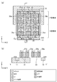
- FIG. 4 It is a figure which shows the example of the basic structure of the standard cell which has a fork sheet FET which concerns on embodiment,
- (a) is a plan view
- (b) is a sectional view.
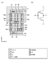
- (A) is a plan view showing a layout structure of a 2-input NAND cell
- (b) is a circuit diagram of a 2-input NAND.
- (A) and (b) are cross-sectional views of the two-input NAND cell of FIG. 2 (a).
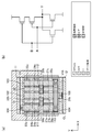
- A) is a plan view showing the layout structure of the tri-state inverter cell
- (b) is a circuit diagram of the tri-state inverter.
- (A) and (b) are cross-sectional views of the tri-state inverter cell of FIG. 4 (a).
- (A) is a plan view showing the layout structure of the inverter cell, and (b) is a circuit diagram of the inverter.
- (A) is a plan view showing a layout structure of a 2-input NOR cell, and (b) is a circuit diagram of a 2-input NOR.
- It is a figure which shows the basic structure of a fork sheet FET (a) is a plan view, (b) is a sectional view.
- the semiconductor integrated circuit apparatus includes a plurality of standard cells (in the present specification, as appropriate, simply referred to as cells), and at least a part of the plurality of standard cells is a nanosheet FET (Field). Effect Transistor) shall be provided.
- the nanosheet FET is an FET using a thin sheet (nanosheet) through which an electric current flows. Nanosheets are made of, for example, silicon. Then, in the semiconductor integrated circuit device, a part of the nanosheet FET is a fork sheet FET having a fork-shaped gate electrode.
- the semiconductor layer portion formed at both ends of the nanosheet and forming the terminal serving as the source or drain of the nanosheet FET is referred to as a "pad".
- the horizontal direction of the drawing is the X direction (corresponding to the first direction)
- the vertical direction of the drawing is the Y direction (corresponding to the second direction)
- the direction perpendicular to the substrate surface is defined. It is in the Z direction (corresponding to the third direction).
- FIG. 10A and 10B are views showing the basic structure of the fork sheet FET, where FIG. 10A is a plan view and FIG. 10B is a cross-sectional view taken along the line YY'of FIG. 10A.
- FIG. 10A is a plan view
- FIG. 10B is a cross-sectional view taken along the line YY'of FIG. 10A.
- two transistors TR1 and TR2 are arranged side by side with an interval S in the Y direction.
- the gate wiring 531 that serves as the gate of the transistor TR1 and the gate wiring 532 that serves as the gate of the transistor TR2 both extend in the Y direction and are arranged at the same position in the X direction.
- the channel portion 521 which is the channel region of the transistor TR1 and the channel portion 526 which is the channel region of the transistor TR2 are composed of nanosheets.
- each of the channel portions 521 and 526 is composed of nanosheets having a three-sheet structure that overlaps in a plan view.
- Pads 522a and 522b serving as a source region or a drain region of the transistor TR1 are formed on both sides of the channel portion 521 in the X direction.
- Pads 527a and 527b serving as a source region or a drain region of the transistor TR2 are formed on both sides of the channel portion 526 in the X direction.
- the pads 522a and 522b are formed by epitaxial growth from the nanosheets constituting the channel portion 521.
- the pads 527a and 527b are formed by epitaxial growth from the nanosheets constituting the channel portion 526.
- the gate wiring 531 surrounds the outer periphery of the channel portion 521 made of nanosheets in the Y direction and the Z direction via a gate insulating film (not shown). However, in the nanosheet constituting the channel portion 521, the surface on the side of the transistor TR2 in the Y direction is not covered by the gate wiring 531 and is exposed from the gate wiring 531. That is, in the cross-sectional view of FIG. 10B, the gate wiring 531 does not cover the right side of the drawing of the nanosheet constituting the channel portion 521, but covers the upper side, the left side, and the lower side of the drawing. The gate wiring 531 overlaps the nanosheet constituting the channel portion 521 on the opposite side of the transistor TR2 in the Y direction by the length OL.
- the gate wiring 532 surrounds the outer periphery of the channel portion 526 made of nanosheets in the Y and Z directions via a gate insulating film (not shown). However, in the nanosheet constituting the channel portion 526, the surface on the side of the transistor TR1 in the Y direction is not covered by the gate wiring 532 and is exposed from the gate wiring 532. That is, in the cross-sectional view of FIG. 10B, the gate wiring 532 does not cover the left side of the drawing of the nanosheet constituting the channel portion 526, but covers the upper side, the right side, and the lower side of the drawing. The gate wiring 532 overlaps the nanosheet constituting the channel portion 526 on the opposite side of the transistor TR1 in the Y direction by the length OL.
- the effective gate width Weff 2 ⁇ W + H Will be. Since the channel portions 521 and 526 of the transistors TR1 and TR2 are composed of three nanosheets, the gate effective width of the transistors TR1 and TR2 is determined. 3x (2xW + H) Will be.
- the gate wiring 531 does not overlap the nanosheet constituting the channel portion 521 on the side of the transistor TR2 in the Y direction. Further, the gate wiring 532 does not overlap with the nanosheet constituting the channel portion 526 on the side of the transistor TR1 in the Y direction. As a result, the transistors TR1 and TR2 can be brought closer to each other, and the area can be reduced.
- the number of nanosheets constituting the channel portion of the transistor is not limited to three. That is, the nanosheet may have a single sheet structure, or may have a plurality of overlapping sheet structures in a plan view. Further, in FIG. 10B, the cross-sectional shape of the nanosheet is shown as a rectangle, but the cross-sectional shape of the nanosheet is not limited to this, and the cross-sectional shape of the nanosheet may be, for example, a square, a circle, an ellipse, or the like. ..
- the fork sheet FET and the nano sheet FET in which the gate wiring surrounds the entire circumference of the nano sheet may be mixed in the semiconductor integrated circuit device.
- VDD and VVSS indicate the power supply voltage or the power supply itself.
- expressions such as “same wiring width” that mean that the widths and the like are the same include a range of manufacturing variation.
- FIG. 1A and 1B are views showing an example of a basic structure of a standard cell having a fork sheet FET according to an embodiment, in which FIG. 1A is a plan view and FIG. 1B is a cross-sectional view taken along the line YY'of FIG. is there.
- FIG. 1A shows the cell frame CL of the standard cell. The same applies to the subsequent plan views.
- the standard cell of FIG. 1 is arranged side by side in the X direction in contact with the cell frame CL together with other standard cells to form a cell row. Further, the plurality of cell rows are arranged side by side in the Y direction in contact with the cell frame CL. However, the plurality of cell columns are flipped upside down every other column.
- power supply wirings 11 and 12 extending in the X direction are provided at both ends of the standard cell in the Y direction, respectively.
- Both the power supply wirings 11 and 12 are embedded power supply wirings (BPR: Buried Power Rail) formed in the embedded wiring layer.
- the power supply wiring 11 supplies the power supply voltage VDD
- the power supply wiring 12 supplies the power supply voltage VSS.
- the power supply wirings 11 and 12 are shared with other cells arranged side by side in the X direction to form a power supply wiring arranged between the cell rows.
- P-type transistors P11, P12, P21, and P22 are formed in the P-type region on the N well.
- N-type transistors N11, N12, N21, and N22 are formed in the N-type region on the P-type substrate.
- the transistors P11, P12, N11, and N12 are arranged in a row in the Y direction.
- the transistors P21, P22, N21, and N22 are arranged in a row in the Y direction.
- the transistors P11, P12, P21, and P22 each have nanosheets 21a, 23a, 21b, and 23b composed of three sheets as channel portions. That is, the transistors P11, P12, P21, and P22 are nanosheet FETs.
- a pad 22a composed of a semiconductor layer having an integral structure connected to three sheets, 22b and 22c are formed, respectively.
- the pads 22a and 22b serve as a source region and a drain region of the transistor P11.
- the pads 22b and 22c serve as a source region and a drain region of the transistor P21.
- Pads 24a, 24b, 24c made of a semiconductor layer having an integral structure connected to three sheets are formed on the left side of the drawing of the nanosheet 23a, between the nanosheets 23a and 23b, and on the right side of the drawing of the nanosheet 23b, respectively.
- the pads 24a and 24b serve as a source region and a drain region of the transistor P12.
- the pads 24b and 24c serve as a source region and a drain region of the transistor P22.
- the transistors N11, N12, N21, and N22 each have nanosheets 26a, 28a, 26b, and 28b composed of three sheets as channel portions. That is, the transistors N11, N12, N21, and N22 are nanosheet FETs.
- a pad 27a composed of a semiconductor layer having an integral structure connected to three sheets, 27b and 27c are formed, respectively.
- the pads 27a and 27b serve as a source region and a drain region of the transistor N11.
- the pads 27b and 27c serve as a source region and a drain region of the transistor N21.
- Pads 29a, 29b, 29c made of a semiconductor layer having an integral structure connected to three sheets are formed on the left side of the drawing of the nanosheet 28a, between the nanosheets 28a and 28b, and on the right side of the drawing of the nanosheet 28b, respectively.
- the pads 29a and 29b serve as a source region and a drain region of the transistor N12.
- the pads 29b and 29c serve as a source region and a drain region of the transistor N22.
- Gate wirings 31 and 32 extending in parallel in the Y direction are formed in the P-shaped region.
- Dummy gate wirings 35a and 35b are formed on the cell frame CLs on both sides of the gate wirings 31 and 32 in the X direction.
- the gate wirings 31 and 32 and the dummy gate wirings 35a and 35b are formed with the same width and are arranged at the same pitch.
- Gate wirings 33 and 34 extending in parallel in the Y direction are formed in the N-type region.
- Dummy gate wirings 35c and 35d are formed on the cell frame CLs on both sides of the gate wirings 33 and 34 in the X direction.
- the gate wirings 33 and 34 and the dummy gate wirings 35c and 35d are formed with the same width and are arranged at the same pitch.
- the gate wiring 31 surrounds the nanosheet 21a of the transistor P11 and the outer periphery of the nanosheet 23a of the transistor P12 in the Y and Z directions via a gate insulating film (not shown).
- the gate wiring 31 serves as a gate for the transistors P11 and P12.
- the gate wiring 32 surrounds the nanosheet 21b of the transistor P21 and the outer periphery of the nanosheet 23b of the transistor P22 in the Y direction and the Z direction via a gate insulating film (not shown).
- the gate wiring 32 serves as a gate for the transistors P21 and P22.
- the gate wiring 33 surrounds the nanosheet 26a of the transistor N11 and the outer periphery of the nanosheet 28a of the transistor N12 in the Y and Z directions via a gate insulating film (not shown).
- the gate wiring 33 serves as a gate for the transistors N11 and N12.
- the gate wiring 34 surrounds the nanosheet 26b of the transistor N21 and the outer periphery of the nanosheet 28b of the transistor N22 in the Y direction and the Z direction via a gate insulating film (not shown).
- the gate wiring 34 serves as a gate for the transistors N21 and N22.
- the surface on the side opposite to the N-shaped region in the Y direction (the surface on the side close to the power supply wiring 11) is not covered by the gate wirings 31 and 32, and from the gate wirings 31 and 32. It is exposed.
- the surface on the N-shaped region side in the Y direction is not covered by the gate wirings 31 and 32, but is exposed from the gate wirings 31 and 32.
- the nanosheets 21a and 23a constitute the first nanosheet group
- the nanosheet 21a corresponds to the first nanosheet farthest from the N-type region in the first nanosheet group
- the nanosheet 23a corresponds to the first nanosheet group. It corresponds to the second nanosheet closest to the N-type region.
- the surface on the P-shaped region side in the Y direction is not covered by the gate wirings 33 and 34, and is exposed from the gate wirings 33 and 34.
- the surface opposite to the P-shaped region in the Y direction (the surface closer to the power supply wiring 12) is not covered by the gate wirings 33 and 34, and is exposed from the gate wirings 33 and 34.
- the nanosheets 26a and 28a constitute the second nanosheet group
- the nanosheet 28a corresponds to the third nanosheet farthest from the P-type region in the second nanosheet group
- the nanosheet 26a is in the second nanosheet group. It corresponds to the 4th nanosheet closest to the P-type region.
- the power supply wirings 11 and 12 are embedded power supply wirings, the present invention is not limited to this, and for example, the power supply wirings may be formed in the upper metal wiring layer.
- transistors are arranged in the X direction, but the present invention is not limited to this.
- only one transistor may be arranged in the X direction, or three or more transistors may be arranged in the X direction. You may be.
- FIG. 2 (a) is a plan view showing the layout structure of the 2-input NAND cell
- FIG. 2 (b) is a circuit diagram of the 2-input NAND
- FIG. 3 (a) is a cross section of line Y1-Y1'of FIG. 2 (a).
- FIG. 3 (b) is a cross-sectional view taken along the line Y2-Y2'of FIG. 2 (a).
- local wirings 41, 42, 43, 44, 45 extending in the Y direction are formed.
- the local wiring 41 is connected to the pads 22a and 24a.
- the local wiring 42 is connected to the pads 22b and 24b, and is also connected to the power supply wiring 11 via vias.
- the local wiring 43 is connected to the pads 22c, 24c, 27c, 29c.
- the local wiring 44 is connected to the pads 27a and 29a, and is also connected to the power supply wiring 12 via vias.
- the local wiring 45 is connected to the pads 27b and 29b.
- the gate wirings 31 and 33 arranged in the Y direction are connected via a bridge portion 36a formed between the gate wiring 31 and the gate wiring 33.
- the gate wirings 32 and 34 arranged in the Y direction are connected via a bridge portion 36b formed between the gate wiring 32 and the gate wiring 34.
- the bridge portions 36a and 36b are examples of gate connection portions.
- metal wirings 51, 52, 53 extending in the X direction are formed.
- the metal wiring 51 is connected to the local wirings 41 and 43 via vias.
- the metal wiring 52 is connected to the gate wirings 32 and 34 via vias.
- the metal wiring 53 is connected to the gate wirings 31 and 33 via vias.
- the metal wirings 51, 52, and 53 correspond to the outputs Y and the inputs A and B of the 2-input NAND, respectively.
- FIG. 4 (a) is a plan view showing the layout structure of the tri-state inverter cell
- FIG. 4 (b) is a circuit diagram of the tri-state inverter
- FIG. 5 (a) is a cross section of line Y1-Y1'of FIG. 4 (a).
- FIG. 4 (b) is a cross-sectional view taken along the line Y2-Y2'of FIG. 4 (a).
- local wirings 61, 62, 63, 64, 65 extending in the Y direction are formed.
- the local wiring 61 is connected to the pads 22a and 24a, and is connected to the power supply wiring 11 via vias.
- the local wiring 62 is connected to the pads 22b and 24b.
- the local wiring 63 is connected to the pads 22c, 24c, 27c, 29c.
- the local wiring 64 is connected to the pads 27a and 29a, and is also connected to the power supply wiring 12 via vias.
- the local wiring 65 is connected to the pads 27b and 29b.
- the gate wirings 31 and 33 arranged in the Y direction are connected via a bridge portion 37 formed between the gate wiring 31 and the gate wiring 33.
- the gate wires 32, 34 lined up in the Y direction are not connected and remain separated.
- metal wirings 71, 72, 73, 74 extending in the X direction are formed.
- the metal wiring 71 is connected to the gate wiring 32 via vias.
- the metal wiring 72 is connected to the gate wirings 31 and 33 via vias.
- the metal wiring 73 is connected to the gate wiring 34 via vias.
- the metal wiring 74 is connected to the local wiring 63 via a via.
- the metal wirings 71, 72, 73, and 74 correspond to the inputs NE, A, E, and the output Y of the tri-state inverter, respectively.
- FIG. 6A is a plan view showing the layout structure of the inverter cell
- FIG. 6B is a circuit diagram of the inverter.
- This inverter cell is based on a basic structure in which only one transistor is arranged in the X direction. In this basic structure, it is assumed that only the transistors P11, P12, N11, and N12 of FIG. 1 are formed.
- local wirings 81, 82, 83 extending in the Y direction are formed.
- the local wiring 81 is connected to the pads 22a and 24a, and is also connected to the power supply wiring 11 via vias.
- the local wiring 82 is connected to the pads 22b, 24b, 27b, 29b.
- the local wiring 83 is connected to the pads 27a and 29a, and is also connected to the power supply wiring 12 via vias.
- the gate wirings 31 and 33 arranged in the Y direction are connected via a bridge portion 38 formed between the gate wiring 31 and the gate wiring 33.
- metal wirings 91 and 92 extending in the X direction are formed.
- the metal wiring 91 is connected to the gate wirings 31 and 33 via vias.
- the metal wiring 92 is connected to the local wiring 82 via a via.
- the metal wirings 91 and 92 correspond to the input A and the output Y of the inverter, respectively.
- FIG. 7A is a plan view showing the layout structure of the 2-input NOR cell
- FIG. 7B is a circuit diagram of the 2-input NOR.
- local wirings 101, 102, 103, 104, 105 extending in the Y direction are formed.
- the local wiring 101 is connected to the pads 22a and 24a, and is also connected to the power supply wiring 11 via vias.
- the local wiring 102 is connected to the pads 22b and 24b.
- the local wiring 103 is connected to the pads 22c, 24c, 27c, 29c.
- the local wiring 104 is connected to the pads 27a and 29a.
- the local wiring 105 is connected to the pads 27b and 29b, and is also connected to the power supply wiring 12 via via vias.
- the gate wirings 31 and 33 arranged in the Y direction are connected via a bridge portion 39a formed between the gate wiring 31 and the gate wiring 33.
- the gate wirings 32 and 34 arranged in the Y direction are connected via a bridge portion 39b formed between the gate wiring 32 and the gate wiring 34.
- metal wirings 111, 112, 113 extending in the X direction are formed.
- the metal wiring 111 is connected to the gate wirings 31 and 33 via vias.
- the metal wiring 112 is connected to the gate wirings 32 and 34 via vias.
- the metal wiring 113 is connected to the local wirings 103 and 104 via vias.
- the metal wirings 111, 112, and 113 correspond to inputs B, A, and output Y of the two-input NOR, respectively.
- the surfaces of the nanosheets 21a and 21b on the side far from the N-type region in the Y direction are exposed from the gate wirings 31 and 32.
- the gate wirings 31 and 32 do not overlap from the nanosheets 21a and 21b to the power supply wiring 11 side.
- the surface on the side far from the P-shaped region in the Y direction is exposed from the gate wirings 33 and 34.
- the gate wirings 33 and 34 do not overlap from the nanosheets 28a and 28b to the power supply wiring 12 side. Therefore, at the boundary between adjacent cells in the Y direction, the space required between the nanosheets of one cell and the nanosheets of the other cell becomes smaller.
- the surface on the N-shaped region side in the Y direction is exposed from the gate wirings 31 and 32.
- the gate wirings 31 and 32 do not overlap from the nanosheets 23a and 23b to the N-type region side.
- the surface on the P-shaped region side in the Y direction is exposed from the gate wirings 33 and 34.
- the gate wirings 33 and 34 do not overlap from the nanosheets 26a and 26b to the P-type region side. Therefore, at the boundary between the P-type region and the N-type region, the space required between the nanosheet in the P-type region and the nanosheet in the N-type region becomes smaller.
- the size of the semiconductor integrated circuit device having the fork sheet FET in the Y direction can be effectively reduced.
- FIG. 8 is a diagram showing a basic structure of a standard cell having a fork sheet FET according to a modified example, (a) is a plan view, and (b) is a cross-sectional view taken along the line YY'of (a).
- the transistors are arranged in three rows in the Y direction in the P-type region on the N-well, and the transistors are arranged in three rows in the Y direction in the N-type region on the P-type substrate. That is, P-type transistors P11, P12, P13, P21, P22, and P23 are formed in the P-type region. N-type transistors N11, N12, N13, N21, N22, and N23 are formed in the N-type region. The transistors P11, P12, P13, N11, N12, and N13 are arranged in a row in the Y direction. The transistors P21, P22, P23, N21, N22, and N23 are arranged in a row in the Y direction.
- the transistors P11, P12, P13, P21, P22, and P23 have nanosheets 121a, 122a, 123a, 121b, 122b, and 123b, which are composed of three sheets, as channel portions, respectively.
- the transistors N11, N12, N13, N21, N22, and N23 have nanosheets 124a, 125a, 126a, 124b, 125b, and 126b, which are composed of three sheets, as channel portions, respectively.
- Gate wirings 131 and 132 extending in parallel in the Y direction are formed in the P-shaped region.
- the gate wiring 131 surrounds the nanosheet 121a of the transistor P11, the nanosheet 122a of the transistor P12, and the outer periphery of the nanosheet 123a of the transistor P13 in the Y and Z directions via a gate insulating film (not shown).
- the gate wiring 131 serves as a gate for the transistors P11, P12, and P13.
- the gate wiring 132 surrounds the nanosheet 121b of the transistor P21, the nanosheet 122b of the transistor P22, and the outer periphery of the nanosheet 123b of the transistor P23 in the Y and Z directions via a gate insulating film (not shown).
- the gate wiring 132 serves as a gate for the transistors P21, P22, and P23.
- Gate wiring 133, 134 extending in parallel in the Y direction is formed in the N-type region.
- the gate wiring 133 surrounds the nanosheet 124a of the transistor N11, the nanosheet 125a of the transistor N12, and the outer periphery of the nanosheet 126a of the transistor N13 in the Y and Z directions via a gate insulating film (not shown).
- the gate wiring 133 serves as a gate for the transistors N11, N12, and N13.
- the gate wiring 134 surrounds the nanosheet 124b of the transistor N21, the nanosheet 125b of the transistor N22, and the outer periphery of the nanosheet 126b of the transistor N23 in the Y and Z directions via a gate insulating film (not shown).
- the gate wiring 134 serves as a gate for the transistors N21, N22, and N23.
- the surface opposite to the N-shaped region in the Y direction is not covered by the gate wirings 131 and 132, and the nanosheets 121a and 121b are formed from the gate wirings 131 and 132. It is exposed.
- the surface on the N-shaped region side in the Y direction is not covered by the gate wirings 131 and 132, but is exposed from the gate wirings 131 and 132.
- the nanosheets 121a, 122a, 123a constitute the first nanosheet group
- the nanosheet 121a corresponds to the first nanosheet farthest from the N-type region in the first nanosheet group
- the nanosheet 123a is the first nanosheet. It corresponds to the second nanosheet closest to the N-type region in the group.
- the surface on the P-shaped region side in the Y direction is not covered by the gate wirings 133 and 134, but is exposed from the gate wirings 133 and 134.
- the surface opposite to the P-shaped region in the Y direction (the surface closer to the power supply wiring 12) is not covered by the gate wiring 133 and 134, and is exposed from the gate wiring 133 and 134.
- the nanosheets 124a, 125a, 126a constitute the second nanosheet group
- the nanosheet 126a corresponds to the third nanosheet farthest from the P-type region in the second nanosheet group
- the nanosheet 124a is the second nanosheet group.
- the nanosheets 122a and 122b are surrounded by gate wirings 131 and 132 all around in the Y direction.
- the entire circumference of the nanosheets 125a and 125b in the Y direction is surrounded by gate wiring 133 and 134.
- the same action and effect as those in the above-described embodiment can be obtained. That is, at the boundary between adjacent cells in the Y direction, the space required between the nanosheets of one cell and the nanosheets of the other cell becomes smaller. Further, at the boundary portion between the P-type region and the N-type region, the space required between the nanosheet in the P-type region and the nanosheet in the N-type region becomes smaller. Therefore, the size of the semiconductor integrated circuit device having the fork sheet FET in the Y direction can be effectively reduced.
- Modification 2 9A and 9B are views showing the basic structure of a standard cell having a fork sheet FET according to a modified example, FIG. 9A is a plan view, and FIG. 9B is a sectional view taken along line YY'of FIG. 9A.
- the transistors are arranged in four rows in the Y direction in the P-type region on the N-well, and the transistors are arranged in four rows in the Y direction in the N-type region on the P-type substrate. That is, P-type transistors P11, P12, P13, P14, P21, P22, P23, and P24 are formed in the P-type region. N-type transistors N11, N12, N13, N14, N21, N22, N23, and N24 are formed in the N-type region. The transistors P11, P12, P13, P14, N11, N12, N13, and N14 are arranged in a row in the Y direction. The transistors P21, P22, P23, P24, N21, N22, N23, and N24 are arranged in a row in the Y direction.
- Transistors P11, P12, P13, P14, P21, P22, P23, P24 have nanosheets 221a, 222a, 223a, 224a, 221b, 222b, 223b, 224b, respectively, as channel portions.
- the transistors N11, N12, N13, N14, N21, N22, N23, and N24 have nanosheets 225a, 226a, 227a, 228a, 225b, 226b, 227b, and 228b, respectively, as channel portions.
- Gate wirings 231 and 232 extending in parallel in the Y direction are formed in the P-shaped region.
- the gate wiring 231 surrounds the nanosheet 221a of the transistor P11 and the outer periphery of the nanosheet 222a of the transistor P12 in the Y and Z directions via a gate insulating film (not shown).
- the gate wiring 231 serves as a gate for the transistors P11 and P12.
- the gate wiring 232 surrounds the nanosheet 221b of the transistor P21 and the outer periphery of the nanosheet 222b of the transistor P22 in the Y direction and the Z direction via a gate insulating film (not shown).
- the gate wiring 232 serves as a gate for the transistors P21 and P22.
- gate wirings 233 and 234 extending in parallel in the Y direction are formed.
- the gate wiring 233 is in the same position as the gate wiring 231 in the X direction, and the gate wiring 234 is in the same position as the gate wiring 232 in the X direction.
- the gate wiring 233 surrounds the nanosheet 223a of the transistor P13 and the outer periphery of the nanosheet 224a of the transistor P14 in the Y and Z directions via a gate insulating film (not shown).
- the gate wiring 233 serves as a gate for the transistors P13 and P14.
- the gate wiring 234 surrounds the nanosheet 223b of the transistor P23 and the outer periphery of the nanosheet 224b of the transistor P24 in the Y direction and the Z direction via a gate insulating film (not shown).
- the gate wiring 234 serves as a gate for the transistors P23 and P24.
- Gate wirings 235 and 236 extending in parallel in the Y direction are formed in the N-shaped region.
- the gate wiring 235 surrounds the nanosheet 225a of the transistor N11 and the outer periphery of the nanosheet 226a of the transistor N12 in the Y and Z directions via a gate insulating film (not shown).
- the gate wiring 235 serves as a gate for the transistors N11 and N12.
- the gate wiring 236 surrounds the nanosheet 225b of the transistor N21 and the outer periphery of the nanosheet 226b of the transistor N22 in the Y direction and the Z direction via a gate insulating film (not shown).
- the gate wiring 236 serves as a gate for the transistors N21 and N22.
- gate wirings 237 and 238 extending in parallel in the Y direction are formed.
- the gate wiring 237 is in the same position as the gate wiring 235 in the X direction, and the gate wiring 238 is in the same position as the gate wiring 236 in the X direction.
- the gate wiring 237 surrounds the nanosheet 227a of the transistor N13 and the outer periphery of the nanosheet 228a of the transistor N14 in the Y and Z directions via a gate insulating film (not shown).
- the gate wiring 237 serves as a gate for the transistors N13 and N14.
- the gate wiring 238 surrounds the nanosheet 227b of the transistor N23 and the outer periphery of the nanosheet 228b of the transistor N24 in the Y direction and the Z direction via a gate insulating film (not shown).
- the gate wiring 238 serves as a gate for the transistors N23 and N24.
- the surface on the side opposite to the N-shaped region in the Y direction (the surface on the side close to the power supply wiring 11) is not covered by the gate wirings 231,232, and the gate wirings 231 and 232 It is exposed.
- the surface on the N-shaped region side in the Y direction is not covered by the gate wirings 233 and 234, but is exposed from the gate wirings 233 and 234.
- the nanosheets 221a, 222a, 223a, 224a constitute the first nanosheet group
- the nanosheet 221a corresponds to the first nanosheet farthest from the N-type region in the first nanosheet group
- the nanosheet 224a is the first nanosheet group. It corresponds to the second nanosheet closest to the N-type region in one nanosheet group.
- the gate wirings 231 and 233 correspond to the first gate wiring.
- the first gate wiring is separated between the nanosheet 222a and the nanosheet 223a.
- nanosheets 225a and 225b the surface on the P-shaped region side in the Y direction is not covered by the gate wirings 235 and 236, and is exposed from the gate wirings 235 and 236.
- the surface opposite to the P-shaped region in the Y direction (the surface closer to the power supply wiring 12) is not covered by the gate wirings 237 and 238, and is exposed from the gate wirings 237 and 238.
- nanosheets 225a, 226a, 227a, 228a constitute the second nanosheet group
- nanosheet 228a corresponds to the third nanosheet farthest from the P-type region in the second nanosheet group
- nanosheet 225a is the second nanosheet group.
- the gate wirings 235 and 237 correspond to the second gate wiring.
- the second gate wiring is separated between the nanosheet 226a and the nanosheet 227a.
- the same action and effect as those in the above-described embodiment can be obtained. That is, at the boundary between adjacent cells in the Y direction, the space required between the nanosheets of one cell and the nanosheets of the other cell becomes smaller. Further, at the boundary portion between the P-type region and the N-type region, the space required between the nanosheet in the P-type region and the nanosheet in the N-type region becomes smaller. Therefore, the size of the semiconductor integrated circuit device having the fork sheet FET in the Y direction can be effectively reduced.
- the surfaces of the nanosheets 222a and 222b facing the nanosheets 223a and 223b are not covered by the gate wirings 231,232 and are exposed from the gate wirings 231,232.
- the surfaces of the nanosheets 223a and 223b facing the nanosheets 222a and 222b are not covered by the gate wirings 233 and 234 and are exposed from the gate wirings 233 and 234.
- the nanosheets 222a and 223a are located between the first nanosheet and the second nanosheet in the first nanosheet group, and correspond to the fifth and sixth nanosheets adjacent to each other in the Y direction.
- the surfaces of the nanosheets 226a and 226b facing the nanosheets 227a and 227b are not covered by the gate wirings 235 and 236 and are exposed from the gate wirings 235 and 236.
- the surfaces of the nanosheets 227a and 227b facing the nanosheets 226a and 226b are not covered by the gate wirings 237 and 238 and are exposed from the gate wirings 237 and 238.
- the nanosheets 226a and 227a are located between the third nanosheet and the fourth nanosheet in the second nanosheet group, and correspond to the seventh and eighth nanosheets adjacent to each other in the Y direction.
- the gate wiring 231 and the gate wiring 233 are separated, different signals can be given to the gates of the transistors P11 and P12 and the gates of the transistors P13 and P14. Since the gate wiring 232 and the gate wiring 234 are separated, different signals can be given to the gates of the transistors P21 and P22 and the gates of the transistors P23 and P24. Further, since the gate wiring 235 and the gate wiring 237 are separated, different signals can be given to the gates of the transistors N11 and N12 and the gates of the transistors N13 and N14. Since the gate wiring 236 and the gate wiring 238 are separated, different signals can be given to the gates of the transistors N21 and N22 and the gates of the transistors N23 and N24. Therefore, the degree of freedom of the logic circuit that can be configured is improved.
- the space required between the transistors P12 and P22 and the transistors P13 and P23, that is, between the nanosheets 222a and 222b and the nanosheets 223a and 223b can be small.
- the space required between the transistors N12 and N22 and the transistors N13 and N23, that is, between the nanosheets 226a and 226b and the nanosheets 227a and 227b can be small. Therefore, the size of the semiconductor integrated circuit device having the fork sheet FET in the Y direction can be further effectively reduced.
- the gate wiring 231,233, the gate wiring 232, 234, the gate wiring 235, 237, and the gate wiring 236, 238 may be integrally formed without being separated from each other.
- a layout structure having a small area can be realized for a semiconductor integrated circuit device using a fork sheet FET, which is useful for, for example, miniaturization of a semiconductor chip and improvement of the degree of integration.
Landscapes
- Design And Manufacture Of Integrated Circuits (AREA)
- Chemical & Material Sciences (AREA)
- Engineering & Computer Science (AREA)
- Crystallography & Structural Chemistry (AREA)
- Nanotechnology (AREA)
Priority Applications (2)
| Application Number | Priority Date | Filing Date | Title |
|---|---|---|---|
| JP2021552462A JP7640861B2 (ja) | 2019-10-18 | 2020-10-16 | 半導体集積回路装置 |
| US17/706,177 US12249637B2 (en) | 2019-10-18 | 2022-03-28 | Semiconductor integrated circuit device |
Applications Claiming Priority (2)
| Application Number | Priority Date | Filing Date | Title |
|---|---|---|---|
| JP2019191324 | 2019-10-18 | ||
| JP2019-191324 | 2019-10-18 |
Related Child Applications (1)
| Application Number | Title | Priority Date | Filing Date |
|---|---|---|---|
| US17/706,177 Continuation US12249637B2 (en) | 2019-10-18 | 2022-03-28 | Semiconductor integrated circuit device |
Publications (1)
| Publication Number | Publication Date |
|---|---|
| WO2021075540A1 true WO2021075540A1 (ja) | 2021-04-22 |
Family
ID=75538092
Family Applications (1)
| Application Number | Title | Priority Date | Filing Date |
|---|---|---|---|
| PCT/JP2020/039062 Ceased WO2021075540A1 (ja) | 2019-10-18 | 2020-10-16 | 半導体集積回路装置 |
Country Status (3)
| Country | Link |
|---|---|
| US (1) | US12249637B2 (https=) |
| JP (1) | JP7640861B2 (https=) |
| WO (1) | WO2021075540A1 (https=) |
Cited By (6)
| Publication number | Priority date | Publication date | Assignee | Title |
|---|---|---|---|---|
| US20220216319A1 (en) * | 2019-10-18 | 2022-07-07 | Socionext Inc. | Semiconductor integrated circuit device |
| WO2023066793A1 (en) * | 2021-10-19 | 2023-04-27 | International Business Machines Corporation | Semiconductor device having hybrid middle of line contacts |
| WO2023209971A1 (ja) * | 2022-04-28 | 2023-11-02 | 株式会社ソシオネクスト | 半導体集積回路装置 |
| WO2025126579A1 (ja) * | 2023-12-14 | 2025-06-19 | 株式会社ソシオネクスト | 半導体集積回路装置 |
| WO2025126580A1 (ja) * | 2023-12-14 | 2025-06-19 | 株式会社ソシオネクスト | 半導体集積回路装置 |
| US12426338B2 (en) | 2021-10-27 | 2025-09-23 | International Business Machines Corporation | Buried power rail with robust connection to a wrap around contact |
Families Citing this family (1)
| Publication number | Priority date | Publication date | Assignee | Title |
|---|---|---|---|---|
| EP4199052B1 (en) * | 2021-12-17 | 2024-08-21 | IMEC vzw | Metallization scheme for an integrated circuit |
Citations (1)
| Publication number | Priority date | Publication date | Assignee | Title |
|---|---|---|---|---|
| WO2018030107A1 (ja) * | 2016-08-08 | 2018-02-15 | 株式会社ソシオネクスト | 半導体集積回路装置 |
Family Cites Families (58)
| Publication number | Priority date | Publication date | Assignee | Title |
|---|---|---|---|---|
| US8653596B2 (en) * | 2012-01-06 | 2014-02-18 | International Business Machines Corporation | Integrated circuit including DRAM and SRAM/logic |
| KR101937851B1 (ko) * | 2012-06-27 | 2019-04-10 | 삼성전자 주식회사 | 반도체 집적 회로, 그 설계 방법 및 제조방법 |
| US8836040B2 (en) * | 2012-11-07 | 2014-09-16 | Qualcomm Incorporated | Shared-diffusion standard cell architecture |
| US9614056B2 (en) | 2014-10-28 | 2017-04-04 | Globalfoundries Inc. | Methods of forming a tri-gate FinFET device |
| JP6003961B2 (ja) * | 2014-11-04 | 2016-10-05 | トヨタ自動車株式会社 | 半導体装置 |
| KR102366975B1 (ko) | 2015-07-30 | 2022-02-25 | 삼성전자주식회사 | 반도체 장치 |
| CN109314080B (zh) * | 2016-07-01 | 2022-09-30 | 株式会社索思未来 | 半导体集成电路装置 |
| US10453850B2 (en) * | 2016-07-19 | 2019-10-22 | Tokyo Electron Limited | Three-dimensional semiconductor device including integrated circuit, transistors and transistor components and method of fabrication |
| JP6974743B2 (ja) * | 2016-08-01 | 2021-12-01 | 株式会社ソシオネクスト | 半導体集積回路装置 |
| WO2018042986A1 (ja) * | 2016-08-29 | 2018-03-08 | 株式会社ソシオネクスト | 半導体集積回路装置 |
| JP7032668B2 (ja) * | 2018-01-12 | 2022-03-09 | 株式会社ソシオネクスト | 半導体集積回路装置 |
| JP7125628B2 (ja) * | 2018-03-01 | 2022-08-25 | 株式会社ソシオネクスト | 半導体装置 |
| US10748901B2 (en) * | 2018-10-22 | 2020-08-18 | International Business Machines Corporation | Interlayer via contacts for monolithic three-dimensional semiconductor integrated circuit devices |
| US10985161B2 (en) * | 2019-05-31 | 2021-04-20 | International Business Machines Corporation | Single diffusion break isolation for gate-all-around field-effect transistor devices |
| US10950610B2 (en) * | 2019-07-18 | 2021-03-16 | Globalfoundries U.S. Inc. | Asymmetric gate cut isolation for SRAM |
| US11114345B2 (en) * | 2019-08-22 | 2021-09-07 | Taiwan Semiconductor Manufacturing Co., Ltd. | IC including standard cells and SRAM cells |
| US11393815B2 (en) * | 2019-08-30 | 2022-07-19 | Taiwan Semiconductor Manufacturing Co., Ltd. | Transistors with varying width nanosheet |
| WO2021048995A1 (ja) | 2019-09-13 | 2021-03-18 | 株式会社日立ハイテク | 半導体装置の製造方法及びプラズマ処理装置 |
| CN114467175B (zh) * | 2019-10-02 | 2025-04-29 | 株式会社索思未来 | 半导体集成电路装置及半导体集成电路装置的制造方法 |
| JP7610128B2 (ja) * | 2019-10-18 | 2025-01-08 | 株式会社ソシオネクスト | 半導体集積回路装置 |
| WO2021075353A1 (ja) * | 2019-10-18 | 2021-04-22 | 株式会社ソシオネクスト | 半導体集積回路装置 |
| JP7640861B2 (ja) * | 2019-10-18 | 2025-03-06 | 株式会社ソシオネクスト | 半導体集積回路装置 |
| WO2021125094A1 (ja) * | 2019-12-19 | 2021-06-24 | 株式会社ソシオネクスト | 半導体記憶装置 |
| CN114868242B (zh) * | 2019-12-20 | 2024-11-12 | 株式会社索思未来 | 半导体存储装置 |
| JP7730024B2 (ja) * | 2020-01-27 | 2025-08-27 | 株式会社ソシオネクスト | 半導体記憶装置 |
| CN115066752B (zh) * | 2020-02-19 | 2025-06-03 | 株式会社索思未来 | 半导体存储装置 |
| CN115136296B (zh) * | 2020-02-25 | 2025-07-08 | 株式会社索思未来 | 半导体集成电路装置 |
| JP7667464B2 (ja) * | 2020-03-11 | 2025-04-23 | 株式会社ソシオネクスト | 半導体集積回路装置 |
| CN115552604A (zh) * | 2020-05-14 | 2022-12-30 | 株式会社索思未来 | 半导体装置及其制造方法 |
| US11398480B2 (en) * | 2020-05-15 | 2022-07-26 | International Business Machines Corporation | Transistor having forked nanosheets with wraparound contacts |
| JP7799195B2 (ja) * | 2020-12-25 | 2026-01-15 | 株式会社ソシオネクスト | 半導体集積回路装置 |
| JP7600701B2 (ja) * | 2021-01-19 | 2024-12-17 | 株式会社ソシオネクスト | 半導体装置 |
| JP7635557B2 (ja) * | 2021-01-19 | 2025-02-26 | 株式会社ソシオネクスト | 半導体装置 |
| CN116830257A (zh) * | 2021-02-15 | 2023-09-29 | 株式会社索思未来 | 半导体集成电路装置 |
| WO2022186012A1 (ja) * | 2021-03-05 | 2022-09-09 | 株式会社ソシオネクスト | 半導体集積回路装置 |
| US12464812B2 (en) * | 2021-04-08 | 2025-11-04 | Taiwan Semiconductor Manufacturing Company, Ltd. | Semiconductor device structure including forksheet transistors and methods of forming the same |
| WO2022224847A1 (ja) * | 2021-04-22 | 2022-10-27 | 株式会社ソシオネクスト | 出力回路 |
| WO2022239681A1 (ja) * | 2021-05-12 | 2022-11-17 | 株式会社ソシオネクスト | 半導体集積回路装置 |
| US12170322B2 (en) * | 2021-05-14 | 2024-12-17 | Samsung Electronics Co., Ltd. | Devices including stacked nanosheet transistors |
| EP4338208A1 (en) * | 2021-06-08 | 2024-03-20 | Huawei Technologies Co., Ltd. | Semiconductor architecture and method of manufacturing semiconductor architecture |
| US12002808B2 (en) * | 2021-08-09 | 2024-06-04 | International Business Machines Corporation | Dual dielectric pillar fork sheet device |
| US11855078B2 (en) * | 2021-08-27 | 2023-12-26 | Taiwan Semiconductor Manufacturing Company, Ltd. | Semiconductor device structure including forksheet transistors and methods of forming the same |
| US12324234B2 (en) * | 2021-09-17 | 2025-06-03 | International Business Machines Corporation | Fork sheet device with better electrostatic control |
| JPWO2023053203A1 (https=) * | 2021-09-28 | 2023-04-06 | ||
| JPWO2023095616A1 (https=) * | 2021-11-29 | 2023-06-01 | ||
| US12268031B2 (en) * | 2021-12-27 | 2025-04-01 | International Business Machines Corporation | Backside power rails and power distribution network for density scaling |
| US20230207563A1 (en) * | 2021-12-29 | 2023-06-29 | International Business Machines Corporation | Gate all around complementary metal-oxide-semiconductor field effect transistors |
| WO2023132264A1 (ja) * | 2022-01-06 | 2023-07-13 | 株式会社ソシオネクスト | 半導体集積回路装置 |
| JP2023119368A (ja) * | 2022-02-16 | 2023-08-28 | 株式会社ソシオネクスト | 半導体記憶装置 |
| WO2023157724A1 (ja) * | 2022-02-16 | 2023-08-24 | 株式会社ソシオネクスト | 半導体記憶装置 |
| WO2023157754A1 (ja) * | 2022-02-17 | 2023-08-24 | 株式会社ソシオネクスト | 半導体記憶装置 |
| JPWO2023167083A1 (https=) * | 2022-03-02 | 2023-09-07 | ||
| US20240170331A1 (en) * | 2022-11-22 | 2024-05-23 | International Business Machines Corporation | Forksheet field effect transistor including self-aligned gate |
| JPWO2024135324A1 (https=) * | 2022-12-22 | 2024-06-27 | ||
| WO2024162070A1 (ja) * | 2023-01-31 | 2024-08-08 | 株式会社ソシオネクスト | 半導体集積回路装置 |
| WO2024162046A1 (ja) * | 2023-01-31 | 2024-08-08 | 株式会社ソシオネクスト | 半導体集積回路装置 |
| JPWO2024162047A1 (https=) * | 2023-01-31 | 2024-08-08 | ||
| KR20240142209A (ko) * | 2023-03-21 | 2024-09-30 | 삼성전자주식회사 | 적층형 집적회로 소자 |
-
2020
- 2020-10-16 JP JP2021552462A patent/JP7640861B2/ja active Active
- 2020-10-16 WO PCT/JP2020/039062 patent/WO2021075540A1/ja not_active Ceased
-
2022
- 2022-03-28 US US17/706,177 patent/US12249637B2/en active Active
Patent Citations (1)
| Publication number | Priority date | Publication date | Assignee | Title |
|---|---|---|---|---|
| WO2018030107A1 (ja) * | 2016-08-08 | 2018-02-15 | 株式会社ソシオネクスト | 半導体集積回路装置 |
Non-Patent Citations (2)
| Title |
|---|
| WECKX P., GUPTA M., ONIKI Y., RAGNARSSON L.-A., HORIGUCHI N., SPESSOT A., VERKEST D., RYCKAERT J., LITTA E. DENTONI, YAKIMETS D., : "Novel forksheet device architecture as ultimate logic scaling device towards 2nm", IEEE INTERNATIONAL ELECTRON DEVICES MEETINGS (IDEM), 7 December 2019 (2019-12-07), pages 36.5.1 - 36.5.4, XP033714586 * |
| WECKX P., RYCKAERT J., PUTCHA V., DE KEERSGIETER A., BOEMMELS J., SCHUDDINCK P., JANG D., YAKIMETS D., BARDON M. G., RAGNARSSON L.: "Stacked nanosheet fork architecture for SRAM design and device co-optimization toward 3 nm", IEEE INTERNATIONAL ELECTRON DEVICES MEETING (IEDM), 2 December 2017 (2017-12-02), pages 20.5.1 - 20.5.4, XP033306012 * |
Cited By (8)
| Publication number | Priority date | Publication date | Assignee | Title |
|---|---|---|---|---|
| US20220216319A1 (en) * | 2019-10-18 | 2022-07-07 | Socionext Inc. | Semiconductor integrated circuit device |
| US12249637B2 (en) * | 2019-10-18 | 2025-03-11 | Socionext Inc. | Semiconductor integrated circuit device |
| WO2023066793A1 (en) * | 2021-10-19 | 2023-04-27 | International Business Machines Corporation | Semiconductor device having hybrid middle of line contacts |
| US12464813B2 (en) | 2021-10-19 | 2025-11-04 | International Business Machines Corporation | Semiconductor device having hybrid middle of line contacts |
| US12426338B2 (en) | 2021-10-27 | 2025-09-23 | International Business Machines Corporation | Buried power rail with robust connection to a wrap around contact |
| WO2023209971A1 (ja) * | 2022-04-28 | 2023-11-02 | 株式会社ソシオネクスト | 半導体集積回路装置 |
| WO2025126579A1 (ja) * | 2023-12-14 | 2025-06-19 | 株式会社ソシオネクスト | 半導体集積回路装置 |
| WO2025126580A1 (ja) * | 2023-12-14 | 2025-06-19 | 株式会社ソシオネクスト | 半導体集積回路装置 |
Also Published As
| Publication number | Publication date |
|---|---|
| JP7640861B2 (ja) | 2025-03-06 |
| US12249637B2 (en) | 2025-03-11 |
| US20220216319A1 (en) | 2022-07-07 |
| JPWO2021075540A1 (https=) | 2021-04-22 |
Similar Documents
| Publication | Publication Date | Title |
|---|---|---|
| JP7640861B2 (ja) | 半導体集積回路装置 | |
| US11784188B2 (en) | Semiconductor integrated circuit device | |
| JP7610128B2 (ja) | 半導体集積回路装置 | |
| US20250157929A1 (en) | Semiconductor integrated circuit device | |
| US12119349B2 (en) | Semiconductor integrated circuit device | |
| JP7376805B2 (ja) | 半導体集積回路装置 | |
| CN109564893B (zh) | 半导体芯片 | |
| CN101315928B (zh) | 具有单元金氧半组件的集成电路的布局方法 | |
| WO2021171969A1 (ja) | 半導体集積回路装置 | |
| WO2018003634A1 (ja) | 半導体集積回路装置 | |
| US20230411246A1 (en) | Semiconductor integrated circuit device | |
| JP7041361B2 (ja) | 半導体集積回路装置 | |
| CN111033720B (zh) | 半导体集成电路装置 | |
| CN101261993A (zh) | 半导体器件 | |
| CN111587484A (zh) | 半导体集成电路装置 | |
| WO2024176933A1 (ja) | 半導体集積回路装置 | |
| WO2025141944A1 (ja) | 半導体集積回路装置 | |
| WO2025211237A1 (ja) | 半導体集積回路装置 |
Legal Events
| Date | Code | Title | Description |
|---|---|---|---|
| 121 | Ep: the epo has been informed by wipo that ep was designated in this application |
Ref document number: 20876771 Country of ref document: EP Kind code of ref document: A1 |
|
| ENP | Entry into the national phase |
Ref document number: 2021552462 Country of ref document: JP Kind code of ref document: A |
|
| NENP | Non-entry into the national phase |
Ref country code: DE |
|
| 122 | Ep: pct application non-entry in european phase |
Ref document number: 20876771 Country of ref document: EP Kind code of ref document: A1 |