JP7600701B2 - 半導体装置 - Google Patents
半導体装置 Download PDFInfo
- Publication number
- JP7600701B2 JP7600701B2 JP2021006441A JP2021006441A JP7600701B2 JP 7600701 B2 JP7600701 B2 JP 7600701B2 JP 2021006441 A JP2021006441 A JP 2021006441A JP 2021006441 A JP2021006441 A JP 2021006441A JP 7600701 B2 JP7600701 B2 JP 7600701B2
- Authority
- JP
- Japan
- Prior art keywords
- transistor
- power supply
- power switch
- power
- supply line
- Prior art date
- Legal status (The legal status is an assumption and is not a legal conclusion. Google has not performed a legal analysis and makes no representation as to the accuracy of the status listed.)
- Active
Links
Images


Classifications
-
- H—ELECTRICITY
- H03—ELECTRONIC CIRCUITRY
- H03K—PULSE TECHNIQUE
- H03K19/00—Logic circuits, i.e. having at least two inputs acting on one output; Inverting circuits
- H03K19/0008—Arrangements for reducing power consumption
- H03K19/0016—Arrangements for reducing power consumption by using a control or a clock signal, e.g. in order to apply power supply
-
- H—ELECTRICITY
- H03—ELECTRONIC CIRCUITRY
- H03K—PULSE TECHNIQUE
- H03K17/00—Electronic switching or gating, i.e. not by contact-making and –breaking
- H03K17/16—Modifications for eliminating interference voltages or currents
- H03K17/161—Modifications for eliminating interference voltages or currents in field-effect transistor switches
-
- H—ELECTRICITY
- H10—SEMICONDUCTOR DEVICES; ELECTRIC SOLID-STATE DEVICES NOT OTHERWISE PROVIDED FOR
- H10D—INORGANIC ELECTRIC SEMICONDUCTOR DEVICES
- H10D89/00—Aspects of integrated devices not covered by groups H10D84/00 - H10D88/00
- H10D89/10—Integrated device layouts
-
- H—ELECTRICITY
- H01—ELECTRIC ELEMENTS
- H01L—SEMICONDUCTOR DEVICES NOT COVERED BY CLASS H10
- H01L23/00—Details of semiconductor or other solid state devices
- H01L23/52—Arrangements for conducting electric current within the device in operation from one component to another, i.e. interconnections, e.g. wires, lead frames
- H01L23/522—Arrangements for conducting electric current within the device in operation from one component to another, i.e. interconnections, e.g. wires, lead frames including external interconnections consisting of a multilayer structure of conductive and insulating layers inseparably formed on the semiconductor body
- H01L23/528—Layout of the interconnection structure
- H01L23/5286—Arrangements of power or ground buses
-
- H—ELECTRICITY
- H03—ELECTRONIC CIRCUITRY
- H03K—PULSE TECHNIQUE
- H03K17/00—Electronic switching or gating, i.e. not by contact-making and –breaking
- H03K17/51—Electronic switching or gating, i.e. not by contact-making and –breaking characterised by the components used
- H03K17/56—Electronic switching or gating, i.e. not by contact-making and –breaking characterised by the components used by the use, as active elements, of semiconductor devices
- H03K17/687—Electronic switching or gating, i.e. not by contact-making and –breaking characterised by the components used by the use, as active elements, of semiconductor devices the devices being field-effect transistors
- H03K17/6871—Electronic switching or gating, i.e. not by contact-making and –breaking characterised by the components used by the use, as active elements, of semiconductor devices the devices being field-effect transistors the output circuit comprising more than one controlled field-effect transistor
-
- H—ELECTRICITY
- H03—ELECTRONIC CIRCUITRY
- H03K—PULSE TECHNIQUE
- H03K19/00—Logic circuits, i.e. having at least two inputs acting on one output; Inverting circuits
- H03K19/0008—Arrangements for reducing power consumption
-
- H—ELECTRICITY
- H03—ELECTRONIC CIRCUITRY
- H03K—PULSE TECHNIQUE
- H03K19/00—Logic circuits, i.e. having at least two inputs acting on one output; Inverting circuits
- H03K19/0008—Arrangements for reducing power consumption
- H03K19/0013—Arrangements for reducing power consumption in field effect transistor circuits
-
- H—ELECTRICITY
- H10—SEMICONDUCTOR DEVICES; ELECTRIC SOLID-STATE DEVICES NOT OTHERWISE PROVIDED FOR
- H10D—INORGANIC ELECTRIC SEMICONDUCTOR DEVICES
- H10D84/00—Integrated devices formed in or on semiconductor substrates that comprise only semiconducting layers, e.g. on Si wafers or on GaAs-on-Si wafers
- H10D84/80—Integrated devices formed in or on semiconductor substrates that comprise only semiconducting layers, e.g. on Si wafers or on GaAs-on-Si wafers characterised by the integration of at least one component covered by groups H10D12/00 or H10D30/00, e.g. integration of IGFETs
- H10D84/82—Integrated devices formed in or on semiconductor substrates that comprise only semiconducting layers, e.g. on Si wafers or on GaAs-on-Si wafers characterised by the integration of at least one component covered by groups H10D12/00 or H10D30/00, e.g. integration of IGFETs of only field-effect components
- H10D84/83—Integrated devices formed in or on semiconductor substrates that comprise only semiconducting layers, e.g. on Si wafers or on GaAs-on-Si wafers characterised by the integration of at least one component covered by groups H10D12/00 or H10D30/00, e.g. integration of IGFETs of only field-effect components of only insulated-gate FETs [IGFET]
- H10D84/834—Integrated devices formed in or on semiconductor substrates that comprise only semiconducting layers, e.g. on Si wafers or on GaAs-on-Si wafers characterised by the integration of at least one component covered by groups H10D12/00 or H10D30/00, e.g. integration of IGFETs of only field-effect components of only insulated-gate FETs [IGFET] comprising FinFETs
Landscapes
- Physics & Mathematics (AREA)
- Engineering & Computer Science (AREA)
- Computer Hardware Design (AREA)
- Computing Systems (AREA)
- General Engineering & Computer Science (AREA)
- Mathematical Physics (AREA)
- Geometry (AREA)
- Condensed Matter Physics & Semiconductors (AREA)
- General Physics & Mathematics (AREA)
- Microelectronics & Electronic Packaging (AREA)
- Power Engineering (AREA)
- Semiconductor Integrated Circuits (AREA)
- Design And Manufacture Of Integrated Circuits (AREA)
- Insulated Gate Type Field-Effect Transistor (AREA)
- Metal-Oxide And Bipolar Metal-Oxide Semiconductor Integrated Circuits (AREA)
Description
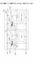
図1は、第1の実施形態における半導体装置のレイアウトの一例を示す。図1に示す半導体装置100は、例えば、少なくとも1つのパワードメインPD1を有する。パワードメインPD1内には、図示しない複数のスタンダードセルが配置されるスタンダードセル領域SCAと、1つまたは複数のRAM(Random Access Memory)が配置される複数の周辺領域PAとが設けられる。スタンダードセル領域SCAは、論理回路が配置される第1領域の一例であり、周辺領域PAは、論理回路とは異なる機能回路が設けられる第2領域の一例である。
図11は、第2の実施形態における半導体装置のレイアウトの一例を示す。図1と同様の要素については、同じ符号を付し、詳細な説明は省略する。図10に示す半導体装置102は、例えば、図1に示したパワードメインPD1におけるX方向の左側に、パワードメインPD2、PD3を有する。
図12は、第3の実施形態における半導体装置のレイアウトの一例を示す。図1と同様の要素については、同じ符号を付し、詳細な説明は省略する。図11に示す半導体装置104は、周辺領域PAにRAMとアナログIPとが配置される。
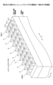
図13は、第4の実施形態における半導体装置のレイアウトの一例を示す。図1と同様の要素については、同じ符号を付し、詳細な説明は省略する。図13に示す半導体装置106は、RAMに隣接する領域に、Y方向にそれぞれ配列される複数の電源スイッチ回路PPSWを含む2つの電源スイッチ回路列が設けられる。すなわち、半導体装置106は、図1の半導体装置100に比べて、電源スイッチ回路PPSWの数が増えている。半導体装置106のその他の構成は、図1の半導体装置100の構成と同様である。
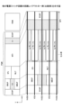
図14は、第5の実施形態における半導体装置のレイアウトの一例を示す。図1と同様の要素については、同じ符号を付し、詳細な説明は省略する。図14に示す半導体装置108は、スタンダードセル領域SCAの周囲に設けられる電源スイッチ領域に配置される複数種の電源スイッチ回路PPSW(PPSWa、PPSWb、PPSWc)を有する。スタンダードセル領域SCAには、図1に示した電源スイッチ回路SPSWが配置されない。このため、スタンダードセル領域SCAに配置される回路の動作電源である電源VVDDは、図示しない上層の配線層を介して電源スイッチ回路PPSWから供給される。
図15は、第6の実施形態における半導体装置のレイアウトの一例を示す。図1および図14と同様の要素については、同じ符号を付し、詳細な説明は省略する。図15に示す半導体装置110は、スタンダードセル領域SCAのY方向の一方に隣接して設けられる電源スイッチ領域に配置される複数種の電源スイッチ回路PPSW(PPSWb、PPSWc、PPSWd、PPSWe)を有する。図14と同様に、スタンダードセル領域SCAには、図1に示した電源スイッチ回路SPSWが配置されない。このため、スタンダードセル領域SCAに配置される回路の動作電源である電源VVDDは、図示しない上層の配線層を介して電源スイッチ回路PPSWから供給される。
ATr1、ATr2 付加トランジスタ
D ドレイン領域
E1、E2 領域
ECAP エンドキャップ
G ゲート電極
MBUF メインバッファ部
MTr メイントランジスタ
PA 周辺領域
PCNT 電源制御信号
PCNT1、PCNT2 電源スイッチ制御回路
PD、PD1、PD2、PD3、PD4 パワードメイン
PPSW、PPSWa、PPSWb 電源スイッチ回路
PPSWc、PPSWd、PPSWe 電源スイッチ回路
PT1、PT2 pチャネルトランジスタ
S ソース領域
SBUF サブバッファ部
SCA スタンダードセル領域
SIG 信号線
SP1 間隔
SPSW 電源スイッチ回路
STr サブトランジスタ
VDD 電源線
VSS 電源線(接地線)
VVDD 仮想電源線
WLT ウェルタップ
Claims (9)
- 論理回路が配置される第1領域と、
前記論理回路とは異なる機能回路が配置される第2領域と、
前記第2領域に隣接して設けられ、第1電源線を前記論理回路および前記機能回路に電源を供給する第2電源線に接続する第1電源スイッチ回路と、
を有し、
前記第1電源スイッチ回路は、
前記論理回路に使用されるトランジスタのサイズより大きいサイズを有し、前記第1電源線を前記第2電源線に接続する第1トランジスタと、
前記機能回路に隣接する領域に設けられたエンドキャップと、
前記第1トランジスタが配置される領域と前記エンドキャップとの間に設けられ、前記論理回路に使用されるトランジスタと同じサイズを有し、前記第1電源線を前記第2電源線に接続する第2トランジスタと、
を有する半導体装置。 - 前記第1領域内に設けられ、前記第1電源線を前記第2電源線に接続する第2電源スイッチ回路を有し、
前記第2電源スイッチ回路は、
前記論理回路に使用されるトランジスタのサイズより大きいサイズを有し、前記第1電源線を前記第2電源線に接続する第3トランジスタと、
前記第3トランジスタにおいて前記第3トランジスタのゲート電極の配列方向の端に隣接して設けられ、前記論理回路に使用されるトランジスタと同じサイズを有し、前記第1電源線を前記第2電源線に接続する第4トランジスタと、
を有し、
前記第4トランジスタが配置される領域の大きさは、前記第1電源スイッチ回路の前記第2トランジスタが配置される領域の大きさと同じである
請求項1に記載の半導体装置。 - 前記第1電源スイッチ回路は、前記第2トランジスタと同じサイズを有し、前記第1電源線を前記第2電源線に接続する第5トランジスタを有する
請求項1または請求項2に記載の半導体装置。 - 前記第1トランジスタおよび前記第2トランジスタの各々は、第1方向に配列される複数のゲート電極を有し、
前記第1トランジスタ、前記第2トランジスタおよび前記エンドキャップは、前記第1方向に沿って配置される
請求項1ないし請求項3のいずれか1項に記載の半導体装置。 - 前記機能回路は、メモリIP、ハードマクロIPまたはアナログIPである
請求項1ないし請求項4のいずれか1項に記載の半導体装置。 - 論理回路が配置される第1領域と、
前記第1領域に隣接して設けられ、第1電源線を前記論理回路に電源を供給する第2電源線に接続する複数種の電源スイッチ回路が配置される電源スイッチ領域と、
を有し、
前記複数種の電源スイッチ回路は、前記論理回路に使用されるトランジスタのサイズより大きいサイズを有し、前記第1電源線を前記第2電源線に接続する第1トランジスタを有し、
前記複数種の電源スイッチ回路の少なくとも1種は、さらに、
前記第1トランジスタが配置される領域において前記第1トランジスタのゲート電極の配列方向である第1方向の端に隣接して設けられ、前記論理回路に使用されるトランジスタと同じサイズを有し、前記第1電源線を前記第2電源線に接続する第2トランジスタと、
前記第2トランジスタが配置される領域において前記第1トランジスタと反対側に隣接して設けられるエンドキャップと、
を有する半導体装置。 - 前記電源スイッチ領域は、前記第1領域の周囲に環状に設けられ、
前記第1領域において前記第1方向の両端に隣接して配置される前記第2トランジスタおよび前記エンドキャップを含む前記電源スイッチ回路は、前記第1トランジスタにおける前記第1方向の両側に設けられた前記第2トランジスタと前記エンドキャップとを有する
請求項6に記載の半導体装置。 - 前記電源スイッチ領域は、前記第1領域において前記第1方向と直交する第2方向に隣接して設けられ、
前記電源スイッチ領域において前記第1方向の両端に配置される前記電源スイッチ回路は、前記第1方向に沿って配置される前記第2トランジスタおよび前記エンドキャップを含み、
前記電源スイッチ領域において前記第1方向の両端に配置される前記電源スイッチ回路を除く前記電源スイッチ回路は、前記第1方向に沿って配置される前記第2トランジスタおよび前記エンドキャップを含まない
請求項6に記載の半導体装置。 - 前記第1トランジスタおよび前記第2トランジスタは、finFETである
請求項1ないし請求項8のいずれか1項に記載の半導体装置。
Priority Applications (5)
| Application Number | Priority Date | Filing Date | Title |
|---|---|---|---|
| JP2021006441A JP7600701B2 (ja) | 2021-01-19 | 2021-01-19 | 半導体装置 |
| CN202210053158.XA CN114823658B (zh) | 2021-01-19 | 2022-01-18 | 半导体装置 |
| US17/577,701 US11563432B2 (en) | 2021-01-19 | 2022-01-18 | Semiconductor device |
| US18/069,084 US11799471B2 (en) | 2021-01-19 | 2022-12-20 | Semiconductor device |
| JP2024206233A JP7736152B2 (ja) | 2021-01-19 | 2024-11-27 | 半導体装置 |
Applications Claiming Priority (1)
| Application Number | Priority Date | Filing Date | Title |
|---|---|---|---|
| JP2021006441A JP7600701B2 (ja) | 2021-01-19 | 2021-01-19 | 半導体装置 |
Related Child Applications (1)
| Application Number | Title | Priority Date | Filing Date |
|---|---|---|---|
| JP2024206233A Division JP7736152B2 (ja) | 2021-01-19 | 2024-11-27 | 半導体装置 |
Publications (2)
| Publication Number | Publication Date |
|---|---|
| JP2022110807A JP2022110807A (ja) | 2022-07-29 |
| JP7600701B2 true JP7600701B2 (ja) | 2024-12-17 |
Family
ID=82405420
Family Applications (2)
| Application Number | Title | Priority Date | Filing Date |
|---|---|---|---|
| JP2021006441A Active JP7600701B2 (ja) | 2021-01-19 | 2021-01-19 | 半導体装置 |
| JP2024206233A Active JP7736152B2 (ja) | 2021-01-19 | 2024-11-27 | 半導体装置 |
Family Applications After (1)
| Application Number | Title | Priority Date | Filing Date |
|---|---|---|---|
| JP2024206233A Active JP7736152B2 (ja) | 2021-01-19 | 2024-11-27 | 半導体装置 |
Country Status (3)
| Country | Link |
|---|---|
| US (2) | US11563432B2 (ja) |
| JP (2) | JP7600701B2 (ja) |
| CN (1) | CN114823658B (ja) |
Families Citing this family (3)
| Publication number | Priority date | Publication date | Assignee | Title |
|---|---|---|---|---|
| CN113767466B (zh) * | 2019-04-25 | 2024-08-02 | 株式会社索思未来 | 半导体装置 |
| WO2021075540A1 (ja) * | 2019-10-18 | 2021-04-22 | 株式会社ソシオネクスト | 半導体集積回路装置 |
| JP7635557B2 (ja) * | 2021-01-19 | 2025-02-26 | 株式会社ソシオネクスト | 半導体装置 |
Citations (5)
| Publication number | Priority date | Publication date | Assignee | Title |
|---|---|---|---|---|
| JP2008103569A (ja) | 2006-10-19 | 2008-05-01 | Nec Electronics Corp | 半導体装置 |
| JP2008251835A (ja) | 2007-03-30 | 2008-10-16 | Renesas Technology Corp | 半導体装置 |
| JP2009289797A (ja) | 2008-05-27 | 2009-12-10 | Nec Electronics Corp | 半導体装置 |
| US20160189759A1 (en) | 2014-12-24 | 2016-06-30 | Samsung Electronics Co., Ltd. | Semiconductor device for reducing an instantaneous voltage drop |
| JP2020004763A (ja) | 2018-06-25 | 2020-01-09 | 株式会社ソシオネクスト | 半導体装置 |
Family Cites Families (13)
| Publication number | Priority date | Publication date | Assignee | Title |
|---|---|---|---|---|
| JP4872264B2 (ja) * | 2005-08-04 | 2012-02-08 | ソニー株式会社 | 半導体集積回路、電源スイッチセル、および、電源スイッチ付き回路セル |
| US20080211568A1 (en) * | 2007-03-01 | 2008-09-04 | Infineon Technologies Ag | MuGFET POWER SWITCH |
| US20090033155A1 (en) * | 2007-06-08 | 2009-02-05 | Renesas Technology Corp. | Semiconductor integrated circuits |
| JP5142686B2 (ja) * | 2007-11-30 | 2013-02-13 | ルネサスエレクトロニクス株式会社 | 半導体集積回路 |
| JP2010225768A (ja) | 2009-03-23 | 2010-10-07 | Toshiba Corp | 半導体装置 |
| JP2012216590A (ja) * | 2011-03-31 | 2012-11-08 | Elpida Memory Inc | 半導体装置 |
| US9070551B2 (en) * | 2013-06-18 | 2015-06-30 | Qualcomm Incorporated | Method and apparatus for a diffusion bridged cell library |
| US9786685B2 (en) | 2015-08-26 | 2017-10-10 | Samsung Electronics Co., Ltd. | Power gate switching system |
| JP6898570B2 (ja) | 2016-06-01 | 2021-07-07 | 株式会社ソシオネクスト | 半導体集積回路装置 |
| JP6825476B2 (ja) * | 2017-04-28 | 2021-02-03 | 株式会社ソシオネクスト | 半導体装置 |
| US10163884B1 (en) * | 2017-08-02 | 2018-12-25 | Qualcomm Incorporated | Cell architecture with intrinsic decoupling capacitor |
| KR102439700B1 (ko) | 2018-01-11 | 2022-09-02 | 삼성전자주식회사 | 반도체 장치, 반도체 장치의 레이아웃 설계 방법 및 반도체 장치의 제조 방법 |
| US11380618B2 (en) | 2018-02-02 | 2022-07-05 | Arm Limited | Power distribution circuitry |
-
2021
- 2021-01-19 JP JP2021006441A patent/JP7600701B2/ja active Active
-
2022
- 2022-01-18 US US17/577,701 patent/US11563432B2/en active Active
- 2022-01-18 CN CN202210053158.XA patent/CN114823658B/zh active Active
- 2022-12-20 US US18/069,084 patent/US11799471B2/en active Active
-
2024
- 2024-11-27 JP JP2024206233A patent/JP7736152B2/ja active Active
Patent Citations (5)
| Publication number | Priority date | Publication date | Assignee | Title |
|---|---|---|---|---|
| JP2008103569A (ja) | 2006-10-19 | 2008-05-01 | Nec Electronics Corp | 半導体装置 |
| JP2008251835A (ja) | 2007-03-30 | 2008-10-16 | Renesas Technology Corp | 半導体装置 |
| JP2009289797A (ja) | 2008-05-27 | 2009-12-10 | Nec Electronics Corp | 半導体装置 |
| US20160189759A1 (en) | 2014-12-24 | 2016-06-30 | Samsung Electronics Co., Ltd. | Semiconductor device for reducing an instantaneous voltage drop |
| JP2020004763A (ja) | 2018-06-25 | 2020-01-09 | 株式会社ソシオネクスト | 半導体装置 |
Also Published As
| Publication number | Publication date |
|---|---|
| CN114823658B (zh) | 2025-08-26 |
| US20220231681A1 (en) | 2022-07-21 |
| US11563432B2 (en) | 2023-01-24 |
| JP7736152B2 (ja) | 2025-09-09 |
| US20230120959A1 (en) | 2023-04-20 |
| JP2022110807A (ja) | 2022-07-29 |
| JP2025019283A (ja) | 2025-02-06 |
| US11799471B2 (en) | 2023-10-24 |
| CN114823658A (zh) | 2022-07-29 |
Similar Documents
| Publication | Publication Date | Title |
|---|---|---|
| JP7736152B2 (ja) | 半導体装置 | |
| US11784188B2 (en) | Semiconductor integrated circuit device | |
| US7989846B2 (en) | Semiconductor device with three-dimensional field effect transistor structure | |
| JP7529121B2 (ja) | 半導体装置 | |
| US20210305278A1 (en) | Semiconductor integrated circuit device | |
| KR100665850B1 (ko) | 고집적 반도체 메모리 소자용 모오스 트랜지스터들의배치구조 및 그에 따른 배치방법 | |
| JP7761168B2 (ja) | 半導体装置 | |
| JPWO2017212644A1 (ja) | 半導体装置 | |
| WO2021075540A1 (ja) | 半導体集積回路装置 | |
| WO2016117288A1 (ja) | 半導体集積回路装置 | |
| JP2004071903A (ja) | 半導体装置 | |
| US6690073B2 (en) | Semiconductor integrated circuit making use of standard cells | |
| JP6970357B2 (ja) | 半導体集積回路装置 | |
| JP2011199034A (ja) | 半導体装置 | |
| JP2024027795A (ja) | 半導体装置 | |
| US20150249052A1 (en) | Semiconductor device | |
| WO2024252660A1 (ja) | 半導体装置 | |
| KR20230041877A (ko) | 반도체 장치 및 그의 제조 방법 | |
| KR20070023458A (ko) | 풀 씨모스형 에스램 셀 |
Legal Events
| Date | Code | Title | Description |
|---|---|---|---|
| A621 | Written request for application examination |
Free format text: JAPANESE INTERMEDIATE CODE: A621 Effective date: 20231222 |
|
| A977 | Report on retrieval |
Free format text: JAPANESE INTERMEDIATE CODE: A971007 Effective date: 20240930 |
|
| TRDD | Decision of grant or rejection written | ||
| A01 | Written decision to grant a patent or to grant a registration (utility model) |
Free format text: JAPANESE INTERMEDIATE CODE: A01 Effective date: 20241105 |
|
| A61 | First payment of annual fees (during grant procedure) |
Free format text: JAPANESE INTERMEDIATE CODE: A61 Effective date: 20241118 |
|
| R150 | Certificate of patent or registration of utility model |
Ref document number: 7600701 Country of ref document: JP Free format text: JAPANESE INTERMEDIATE CODE: R150 |