JP7635557B2 - 半導体装置 - Google Patents
半導体装置 Download PDFInfo
- Publication number
- JP7635557B2 JP7635557B2 JP2021006440A JP2021006440A JP7635557B2 JP 7635557 B2 JP7635557 B2 JP 7635557B2 JP 2021006440 A JP2021006440 A JP 2021006440A JP 2021006440 A JP2021006440 A JP 2021006440A JP 7635557 B2 JP7635557 B2 JP 7635557B2
- Authority
- JP
- Japan
- Prior art keywords
- power supply
- supply line
- power
- wiring
- layer
- Prior art date
- Legal status (The legal status is an assumption and is not a legal conclusion. Google has not performed a legal analysis and makes no representation as to the accuracy of the status listed.)
- Active
Links
- 239000004065 semiconductor Substances 0.000 title claims description 49
- 239000010410 layer Substances 0.000 description 151
- 238000010586 diagram Methods 0.000 description 10
- 102100027582 Nuclear pore complex protein Nup85 Human genes 0.000 description 9
- 101150031080 nup85 gene Proteins 0.000 description 9
- 239000000758 substrate Substances 0.000 description 9
- 239000002184 metal Substances 0.000 description 7
- 230000002093 peripheral effect Effects 0.000 description 7
- 101100325756 Arabidopsis thaliana BAM5 gene Proteins 0.000 description 6
- 101150046378 RAM1 gene Proteins 0.000 description 6
- 101100476489 Rattus norvegicus Slc20a2 gene Proteins 0.000 description 6
- 101001117010 Homo sapiens Pericentrin Proteins 0.000 description 5
- 102100024315 Pericentrin Human genes 0.000 description 5
- 230000000694 effects Effects 0.000 description 5
- 102100031584 Cell division cycle-associated 7-like protein Human genes 0.000 description 4
- 101000777638 Homo sapiens Cell division cycle-associated 7-like protein Proteins 0.000 description 4
- 239000011229 interlayer Substances 0.000 description 3
- 238000002955 isolation Methods 0.000 description 3
- 229910003460 diamond Inorganic materials 0.000 description 2
- 239000010432 diamond Substances 0.000 description 2
- 238000000034 method Methods 0.000 description 2
- 239000002070 nanowire Substances 0.000 description 2
- 230000003071 parasitic effect Effects 0.000 description 2
- 230000000295 complement effect Effects 0.000 description 1
- 238000000605 extraction Methods 0.000 description 1
- 239000002135 nanosheet Substances 0.000 description 1
Images


Classifications
-
- H—ELECTRICITY
- H01—ELECTRIC ELEMENTS
- H01L—SEMICONDUCTOR DEVICES NOT COVERED BY CLASS H10
- H01L23/00—Details of semiconductor or other solid state devices
- H01L23/52—Arrangements for conducting electric current within the device in operation from one component to another, i.e. interconnections, e.g. wires, lead frames
- H01L23/522—Arrangements for conducting electric current within the device in operation from one component to another, i.e. interconnections, e.g. wires, lead frames including external interconnections consisting of a multilayer structure of conductive and insulating layers inseparably formed on the semiconductor body
- H01L23/5226—Via connections in a multilevel interconnection structure
-
- H—ELECTRICITY
- H01—ELECTRIC ELEMENTS
- H01L—SEMICONDUCTOR DEVICES NOT COVERED BY CLASS H10
- H01L23/00—Details of semiconductor or other solid state devices
- H01L23/52—Arrangements for conducting electric current within the device in operation from one component to another, i.e. interconnections, e.g. wires, lead frames
- H01L23/522—Arrangements for conducting electric current within the device in operation from one component to another, i.e. interconnections, e.g. wires, lead frames including external interconnections consisting of a multilayer structure of conductive and insulating layers inseparably formed on the semiconductor body
- H01L23/528—Layout of the interconnection structure
- H01L23/5286—Arrangements of power or ground buses
-
- H—ELECTRICITY
- H10—SEMICONDUCTOR DEVICES; ELECTRIC SOLID-STATE DEVICES NOT OTHERWISE PROVIDED FOR
- H10D—INORGANIC ELECTRIC SEMICONDUCTOR DEVICES
- H10D84/00—Integrated devices formed in or on semiconductor substrates that comprise only semiconducting layers, e.g. on Si wafers or on GaAs-on-Si wafers
- H10D84/90—Masterslice integrated circuits
- H10D84/903—Masterslice integrated circuits comprising field effect technology
- H10D84/907—CMOS gate arrays
-
- H—ELECTRICITY
- H10—SEMICONDUCTOR DEVICES; ELECTRIC SOLID-STATE DEVICES NOT OTHERWISE PROVIDED FOR
- H10D—INORGANIC ELECTRIC SEMICONDUCTOR DEVICES
- H10D89/00—Aspects of integrated devices not covered by groups H10D84/00 - H10D88/00
- H10D89/10—Integrated device layouts
-
- H—ELECTRICITY
- H10—SEMICONDUCTOR DEVICES; ELECTRIC SOLID-STATE DEVICES NOT OTHERWISE PROVIDED FOR
- H10D—INORGANIC ELECTRIC SEMICONDUCTOR DEVICES
- H10D84/00—Integrated devices formed in or on semiconductor substrates that comprise only semiconducting layers, e.g. on Si wafers or on GaAs-on-Si wafers
- H10D84/90—Masterslice integrated circuits
- H10D84/903—Masterslice integrated circuits comprising field effect technology
- H10D84/907—CMOS gate arrays
- H10D84/968—Macro-architecture
- H10D84/974—Layout specifications, i.e. inner core regions
- H10D84/981—Power supply lines
Landscapes
- Physics & Mathematics (AREA)
- Engineering & Computer Science (AREA)
- Microelectronics & Electronic Packaging (AREA)
- General Physics & Mathematics (AREA)
- Condensed Matter Physics & Semiconductors (AREA)
- Computer Hardware Design (AREA)
- Power Engineering (AREA)
- Geometry (AREA)
- Semiconductor Integrated Circuits (AREA)
- Design And Manufacture Of Integrated Circuits (AREA)
- Internal Circuitry In Semiconductor Integrated Circuit Devices (AREA)
- Metal-Oxide And Bipolar Metal-Oxide Semiconductor Integrated Circuits (AREA)
- General Engineering & Computer Science (AREA)
Description
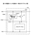
図1は、第1の実施形態における半導体装置のレイアウトの一例を示す。図1に示す半導体装置100は、例えば、少なくとも1つのパワードメインPDを有する。パワードメインPD内には、図示しない複数のスタンダードセルが配置されるスタンダードセル領域SCAが設けられる。特に限定されないが、半導体装置100に搭載されるトランジスタは、finFETである。finFETについては、図5で説明する。スタンダードセル領域SCAは、論理回路を配置可能な第1領域の一例である。
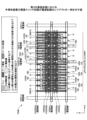
図7は、第2の実施形態における半導体装置の電源スイッチ回路のレイアウトの一例を示す。図3と同様の要素については、同じ符号を付し、詳細な説明は省略する。図7に示す電源スイッチ回路PSW1を有する半導体装置のレイアウトは、図1の半導体装置100のレイアウトと同様である。すなわち、図7に示す電源スイッチ回路PSW1を有する半導体装置は、パワードメインPD内に複数のスタンダードセルが配置されるスタンダードセル領域SCAを有し、電源スイッチ回路PSW1は、スタンダードセル領域SCA内に配置される。
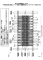
図8は、第3の実施形態における半導体装置の電源スイッチ回路のレイアウトの一例を示す。図3および図7と同様の要素については、同じ符号を付し、詳細な説明は省略する。図8に示す電源スイッチ回路PSW1を有する半導体装置のレイアウトは、図1の半導体装置100のレイアウトと同様である。すなわち、図8に示す電源スイッチ回路PSW1を有する半導体装置は、パワードメインPD内に複数のスタンダードセルが配置されるスタンダードセル領域SCAを有し、電源スイッチ回路PSW1は、スタンダードセル領域SCA内に配置される。
図9は、第4の実施形態における半導体装置の電源スイッチ回路のレイアウトの一例を示す。図3、図7および図8と同様の要素については、同じ符号を付し、詳細な説明は省略する。図9に示す電源スイッチ回路PSW1を有する半導体装置のレイアウトは、図1の半導体装置100のレイアウトと同様である。すなわち、図9に示す電源スイッチ回路PSW1を有する半導体装置は、パワードメインPD内に複数のスタンダードセルが配置されるスタンダードセル領域SCAを有し、電源スイッチ回路PSW1は、スタンダードセル領域SCA内に配置される。
図10は、第5の実施形態における半導体装置のレイアウトの一例を示す。図1と同様の要素については、同じ符号を付し、詳細な説明は省略する。図10に示す半導体装置102は、パワードメインPD内において、スタンダードセル領域SCAを囲むエンドキャップECAPの周囲にサイズの大きいRAM(Random Access Memory)1とサイズが小さいRAM2とがそれぞれ配置される複数の周辺領域PAを有する。RAM1およびRAM2は、所定の機能を有する機能回路の一例である。周辺領域PAは、第2領域の一例である。
図11は、第6の実施形態における半導体装置のレイアウトの一例を示す。図1および図10と同様の要素については、同じ符号を付し、詳細な説明は省略する。図11に示す半導体装置104は、パワードメインPD内において、X方向のRAM2側の端に、レイアウトサイズが電源スイッチ回路PSW1より小さい複数の電源スイッチ回路PSW2が配置される。電源スイッチ回路PSW2を除く構成は、図10と同様である。電源スイッチ回路PSW2は、第2電源スイッチ回路の一例である。
D ドレイン領域
ECAP エンドキャップ
G ゲート電極
H1 間隔
PA 周辺領域
PCNT 電源制御信号
PCNT1 電源スイッチ制御回路
PD パワードメイン
PSW1、PSW2 電源スイッチ回路
PT pチャネルトランジスタ
S ソース領域
SCA スタンダードセル領域
SIG 信号線
VDD 電源線
VSS 電源線(接地線)
VVDD 仮想電源線
W1 間隔
Claims (10)
- 第1配線層に形成され、平面視で第1方向に延在し、第1の電圧が供給される第1電源線と、
前記第1配線層に形成され、前記第1方向に延在し、第2の電圧が供給される第2電源線と、
前記第1配線層の1つ上の配線層である第2配線層に形成され、平面視で前記第1方向とは異なる第2方向に延在し、前記第1電源線と接続し、前記第1の電圧が供給される第3電源線と、
前記第2配線層に形成され、前記第2方向に延在し、前記第2電源線と接続し、前記第2の電圧が供給される第4電源線と、
前記第1配線層に形成され、第3の電圧が供給される第5電源線と、
前記第1電源線と前記第5電源線との間に設けられたトランジスタを有する第1電源スイッチ回路とを有し、
前記トランジスタは、前記第3電源線または前記第4電源線の少なくともいずれかと平面視で重なって位置し、
前記第1電源スイッチ回路は、
前記第2配線層に形成され、前記トランジスタのソース領域および前記第5電源線に電気的に接続し、前記第2方向に延在し、前記トランジスタ上であって平面視で前記第3電源線および前記第4電源線と重ならず、前記第3の電圧が供給される第1配線と、
前記第2配線層に形成され、前記トランジスタのドレイン領域および前記第3電源線に電気的に接続し、前記第2方向に延在し、前記トランジスタ上であって平面視で前記第3電源線および前記第4電源線と重ならず、前記第1の電圧が供給される第2配線と、
を有する半導体装置。 - 前記第1電源スイッチ回路は、前記トランジスタ上で前記第1方向に延在し、前記ドレイン領域および前記第2配線と電気的に接続する第3配線を有し、
前記トランジスタ上で、前記第3電源線と前記第3配線がビアを介して接続される
請求項1に記載の半導体装置。 - 前記第4電源線は、前記トランジスタ上でビアを介して前記第2電源線に接続される
請求項1または請求項2に記載の半導体装置。 - 前記第3電源線および前記第4電源線をそれぞれ複数有し、
前記第1電源スイッチ回路を複数有し、
前記第3電源線および前記第4電源線は、前記第1方向において第1のピッチで繰り返し配置され、
前記複数の第1電源スイッチ回路は、前記第3電源線および前記第4電源線の少なくともいずれかと平面視で重なる前記トランジスタの位置が互いに同じである
請求項1ないし請求項3のいずれか1項に記載の半導体装置。 - 前記第1電源線、前記第2電源線、前記第3電源線、前記第4電源線および前記第1電源スイッチ回路を有し、論理回路が配置された第1領域を有し、
前記第1領域内において、前記第1電源スイッチ回路の配置頻度が、他の部分と比べて前記第1電源スイッチ回路の配置頻度の高い部分を有する
請求項1ないし請求項4のいずれか1項に記載の半導体装置。 - 前記第1領域と隣接して、前記論理回路と異なる機能回路を有する第2領域を有し、
前記配置頻度の高い部分は、前記第2領域と隣接する
請求項5に記載の半導体装置。 - 前記第1領域に配置され、前記第3電源線および前記第4電源線が平面視で重ならないトランジスタを含む第2電源スイッチ回路を有する
請求項5または請求項6に記載の半導体装置。 - 前記トランジスタは、finFETである
請求項1ないし請求項7のいずれか1項に記載の半導体装置。 - 前記トランジスタは、前記第1方向に配列される複数の前記ソース領域と、前記第1方向に配列される複数の前記ドレイン領域と、を有し、
複数の前記ソース領域にそれぞれ対応して設けられる複数の前記第1配線と、
複数の前記ドレイン領域にそれぞれ対応して設けられる複数の前記第2配線と、を有する
請求項1ないし請求項8のいずれか1項に記載の半導体装置。 - 前記トランジスタと重なる前記第3電源線または前記第4電源線の少なくともいずれかは、前記第1方向で、交互に配置された前記第1配線と前記第2配線の複数の群の間に位置する
請求項9に記載の半導体装置。
Priority Applications (5)
| Application Number | Priority Date | Filing Date | Title |
|---|---|---|---|
| JP2021006440A JP7635557B2 (ja) | 2021-01-19 | 2021-01-19 | 半導体装置 |
| CN202210054003.8A CN114823659B (zh) | 2021-01-19 | 2022-01-18 | 半导体装置 |
| US17/577,994 US12283542B2 (en) | 2021-01-19 | 2022-01-18 | Power supply line arrangement having power switch circuit |
| JP2025016202A JP7761168B2 (ja) | 2021-01-19 | 2025-02-03 | 半導体装置 |
| US19/088,339 US20250246539A1 (en) | 2021-01-19 | 2025-03-24 | Power supply line arrangement having power switch circuit |
Applications Claiming Priority (1)
| Application Number | Priority Date | Filing Date | Title |
|---|---|---|---|
| JP2021006440A JP7635557B2 (ja) | 2021-01-19 | 2021-01-19 | 半導体装置 |
Related Child Applications (1)
| Application Number | Title | Priority Date | Filing Date |
|---|---|---|---|
| JP2025016202A Division JP7761168B2 (ja) | 2021-01-19 | 2025-02-03 | 半導体装置 |
Publications (2)
| Publication Number | Publication Date |
|---|---|
| JP2022110806A JP2022110806A (ja) | 2022-07-29 |
| JP7635557B2 true JP7635557B2 (ja) | 2025-02-26 |
Family
ID=82405392
Family Applications (2)
| Application Number | Title | Priority Date | Filing Date |
|---|---|---|---|
| JP2021006440A Active JP7635557B2 (ja) | 2021-01-19 | 2021-01-19 | 半導体装置 |
| JP2025016202A Active JP7761168B2 (ja) | 2021-01-19 | 2025-02-03 | 半導体装置 |
Family Applications After (1)
| Application Number | Title | Priority Date | Filing Date |
|---|---|---|---|
| JP2025016202A Active JP7761168B2 (ja) | 2021-01-19 | 2025-02-03 | 半導体装置 |
Country Status (3)
| Country | Link |
|---|---|
| US (2) | US12283542B2 (ja) |
| JP (2) | JP7635557B2 (ja) |
| CN (1) | CN114823659B (ja) |
Families Citing this family (4)
| Publication number | Priority date | Publication date | Assignee | Title |
|---|---|---|---|---|
| WO2020217396A1 (ja) * | 2019-04-25 | 2020-10-29 | 株式会社ソシオネクスト | 半導体装置 |
| JP7640861B2 (ja) * | 2019-10-18 | 2025-03-06 | 株式会社ソシオネクスト | 半導体集積回路装置 |
| US12438078B2 (en) * | 2022-04-19 | 2025-10-07 | Globalfoundries U.S. Inc. | Local interconnect power rails and upper power rails |
| CN117688889A (zh) * | 2022-09-02 | 2024-03-12 | 长鑫存储技术有限公司 | 版图结构、半导体结构以及存储器 |
Citations (3)
| Publication number | Priority date | Publication date | Assignee | Title |
|---|---|---|---|---|
| JP2020004763A (ja) | 2018-06-25 | 2020-01-09 | 株式会社ソシオネクスト | 半導体装置 |
| US20200042668A1 (en) | 2018-07-31 | 2020-02-06 | Taiwan Semiconductor Manufacturing Company Ltd. | Power structure with power pick-up cell connecting to buried power rail |
| JP2020155505A (ja) | 2019-03-19 | 2020-09-24 | 株式会社東芝 | 半導体装置 |
Family Cites Families (10)
| Publication number | Priority date | Publication date | Assignee | Title |
|---|---|---|---|---|
| JP4200926B2 (ja) * | 2004-03-10 | 2008-12-24 | ソニー株式会社 | 半導体集積回路 |
| JP4535136B2 (ja) * | 2008-01-17 | 2010-09-01 | ソニー株式会社 | 半導体集積回路、および、スイッチの配置配線方法 |
| JP2014067811A (ja) * | 2012-09-25 | 2014-04-17 | Ps4 Luxco S A R L | 半導体装置 |
| US9786685B2 (en) | 2015-08-26 | 2017-10-10 | Samsung Electronics Co., Ltd. | Power gate switching system |
| EP3229270A1 (en) * | 2016-04-06 | 2017-10-11 | IMEC vzw | Integrated circuit power distribution network |
| CN109155284B (zh) | 2016-06-01 | 2022-09-23 | 株式会社索思未来 | 半导体集成电路装置 |
| JP6825476B2 (ja) | 2017-04-28 | 2021-02-03 | 株式会社ソシオネクスト | 半導体装置 |
| KR102439700B1 (ko) | 2018-01-11 | 2022-09-02 | 삼성전자주식회사 | 반도체 장치, 반도체 장치의 레이아웃 설계 방법 및 반도체 장치의 제조 방법 |
| US11380618B2 (en) | 2018-02-02 | 2022-07-05 | Arm Limited | Power distribution circuitry |
| JP7600701B2 (ja) * | 2021-01-19 | 2024-12-17 | 株式会社ソシオネクスト | 半導体装置 |
-
2021
- 2021-01-19 JP JP2021006440A patent/JP7635557B2/ja active Active
-
2022
- 2022-01-18 US US17/577,994 patent/US12283542B2/en active Active
- 2022-01-18 CN CN202210054003.8A patent/CN114823659B/zh active Active
-
2025
- 2025-02-03 JP JP2025016202A patent/JP7761168B2/ja active Active
- 2025-03-24 US US19/088,339 patent/US20250246539A1/en active Pending
Patent Citations (3)
| Publication number | Priority date | Publication date | Assignee | Title |
|---|---|---|---|---|
| JP2020004763A (ja) | 2018-06-25 | 2020-01-09 | 株式会社ソシオネクスト | 半導体装置 |
| US20200042668A1 (en) | 2018-07-31 | 2020-02-06 | Taiwan Semiconductor Manufacturing Company Ltd. | Power structure with power pick-up cell connecting to buried power rail |
| JP2020155505A (ja) | 2019-03-19 | 2020-09-24 | 株式会社東芝 | 半導体装置 |
Also Published As
| Publication number | Publication date |
|---|---|
| US20220231053A1 (en) | 2022-07-21 |
| JP7761168B2 (ja) | 2025-10-28 |
| JP2025066168A (ja) | 2025-04-22 |
| CN114823659A (zh) | 2022-07-29 |
| CN114823659B (zh) | 2025-05-13 |
| US20250246539A1 (en) | 2025-07-31 |
| US12283542B2 (en) | 2025-04-22 |
| JP2022110806A (ja) | 2022-07-29 |
Similar Documents
| Publication | Publication Date | Title |
|---|---|---|
| JP7635557B2 (ja) | 半導体装置 | |
| US8975712B2 (en) | Densely packed standard cells for integrated circuit products, and methods of making same | |
| US10217742B2 (en) | Semiconductor device having dummy active fin patterns | |
| US12310103B2 (en) | Semiconductor integrated circuit device having standard cells including three dimensional transistors | |
| JP7736152B2 (ja) | 半導体装置 | |
| US20020003270A1 (en) | Semiconductor device | |
| WO2018042986A1 (ja) | 半導体集積回路装置 | |
| CN101315928B (zh) | 具有单元金氧半组件的集成电路的布局方法 | |
| CN113327910A (zh) | 用于栅极绑定关断的新颖标准单元架构 | |
| WO2018003634A1 (ja) | 半導体集積回路装置 | |
| WO2021075540A1 (ja) | 半導体集積回路装置 | |
| US6690073B2 (en) | Semiconductor integrated circuit making use of standard cells | |
| US20250120174A1 (en) | Wiring in diffusion breaks in an integrated circuit | |
| JPH0558582B2 (ja) | ||
| JP2011199034A (ja) | 半導体装置 | |
| JP4872264B2 (ja) | 半導体集積回路、電源スイッチセル、および、電源スイッチ付き回路セル | |
| US20150249052A1 (en) | Semiconductor device | |
| KR20230041877A (ko) | 반도체 장치 및 그의 제조 방법 |
Legal Events
| Date | Code | Title | Description |
|---|---|---|---|
| A621 | Written request for application examination |
Free format text: JAPANESE INTERMEDIATE CODE: A621 Effective date: 20231222 |
|
| A977 | Report on retrieval |
Free format text: JAPANESE INTERMEDIATE CODE: A971007 Effective date: 20240930 |
|
| A131 | Notification of reasons for refusal |
Free format text: JAPANESE INTERMEDIATE CODE: A131 Effective date: 20241105 |
|
| A521 | Request for written amendment filed |
Free format text: JAPANESE INTERMEDIATE CODE: A523 Effective date: 20241224 |
|
| TRDD | Decision of grant or rejection written | ||
| A01 | Written decision to grant a patent or to grant a registration (utility model) |
Free format text: JAPANESE INTERMEDIATE CODE: A01 Effective date: 20250114 |
|
| A61 | First payment of annual fees (during grant procedure) |
Free format text: JAPANESE INTERMEDIATE CODE: A61 Effective date: 20250127 |
|
| R150 | Certificate of patent or registration of utility model |
Ref document number: 7635557 Country of ref document: JP Free format text: JAPANESE INTERMEDIATE CODE: R150 |