WO2022224847A1 - 出力回路 - Google Patents
出力回路 Download PDFInfo
- Publication number
- WO2022224847A1 WO2022224847A1 PCT/JP2022/017394 JP2022017394W WO2022224847A1 WO 2022224847 A1 WO2022224847 A1 WO 2022224847A1 JP 2022017394 W JP2022017394 W JP 2022017394W WO 2022224847 A1 WO2022224847 A1 WO 2022224847A1
- Authority
- WO
- WIPO (PCT)
- Prior art keywords
- wiring
- power supply
- output
- extending
- semiconductor chip
- Prior art date
Links
- 239000004065 semiconductor Substances 0.000 claims abstract description 155
- 239000010410 layer Substances 0.000 description 161
- 238000010586 diagram Methods 0.000 description 20
- 239000000758 substrate Substances 0.000 description 13
- 238000012986 modification Methods 0.000 description 11
- 230000004048 modification Effects 0.000 description 11
- 239000002184 metal Substances 0.000 description 6
- 101150071403 INP1 gene Proteins 0.000 description 5
- 101150016601 INP2 gene Proteins 0.000 description 5
- 101100396986 Saccharomyces cerevisiae (strain ATCC 204508 / S288c) INN1 gene Proteins 0.000 description 5
- 230000000694 effects Effects 0.000 description 5
- 230000005669 field effect Effects 0.000 description 4
- 230000002093 peripheral effect Effects 0.000 description 2
- 230000010354 integration Effects 0.000 description 1
- 238000000034 method Methods 0.000 description 1
- 239000002135 nanosheet Substances 0.000 description 1
- 229910052710 silicon Inorganic materials 0.000 description 1
- 239000010703 silicon Substances 0.000 description 1
- 239000002356 single layer Substances 0.000 description 1
Images


Classifications
-
- H—ELECTRICITY
- H01—ELECTRIC ELEMENTS
- H01L—SEMICONDUCTOR DEVICES NOT COVERED BY CLASS H10
- H01L27/00—Devices consisting of a plurality of semiconductor or other solid-state components formed in or on a common substrate
- H01L27/02—Devices consisting of a plurality of semiconductor or other solid-state components formed in or on a common substrate including semiconductor components specially adapted for rectifying, oscillating, amplifying or switching and having at least one potential-jump barrier or surface barrier; including integrated passive circuit elements with at least one potential-jump barrier or surface barrier
- H01L27/0203—Particular design considerations for integrated circuits
- H01L27/0207—Geometrical layout of the components, e.g. computer aided design; custom LSI, semi-custom LSI, standard cell technique
-
- H—ELECTRICITY
- H01—ELECTRIC ELEMENTS
- H01L—SEMICONDUCTOR DEVICES NOT COVERED BY CLASS H10
- H01L27/00—Devices consisting of a plurality of semiconductor or other solid-state components formed in or on a common substrate
- H01L27/02—Devices consisting of a plurality of semiconductor or other solid-state components formed in or on a common substrate including semiconductor components specially adapted for rectifying, oscillating, amplifying or switching and having at least one potential-jump barrier or surface barrier; including integrated passive circuit elements with at least one potential-jump barrier or surface barrier
- H01L27/04—Devices consisting of a plurality of semiconductor or other solid-state components formed in or on a common substrate including semiconductor components specially adapted for rectifying, oscillating, amplifying or switching and having at least one potential-jump barrier or surface barrier; including integrated passive circuit elements with at least one potential-jump barrier or surface barrier the substrate being a semiconductor body
- H01L27/10—Devices consisting of a plurality of semiconductor or other solid-state components formed in or on a common substrate including semiconductor components specially adapted for rectifying, oscillating, amplifying or switching and having at least one potential-jump barrier or surface barrier; including integrated passive circuit elements with at least one potential-jump barrier or surface barrier the substrate being a semiconductor body including a plurality of individual components in a repetitive configuration
- H01L27/118—Masterslice integrated circuits
- H01L27/11803—Masterslice integrated circuits using field effect technology
- H01L27/11807—CMOS gate arrays
-
- H—ELECTRICITY
- H01—ELECTRIC ELEMENTS
- H01L—SEMICONDUCTOR DEVICES NOT COVERED BY CLASS H10
- H01L21/00—Processes or apparatus adapted for the manufacture or treatment of semiconductor or solid state devices or of parts thereof
- H01L21/70—Manufacture or treatment of devices consisting of a plurality of solid state components formed in or on a common substrate or of parts thereof; Manufacture of integrated circuit devices or of parts thereof
- H01L21/77—Manufacture or treatment of devices consisting of a plurality of solid state components or integrated circuits formed in, or on, a common substrate
- H01L21/78—Manufacture or treatment of devices consisting of a plurality of solid state components or integrated circuits formed in, or on, a common substrate with subsequent division of the substrate into plural individual devices
- H01L21/82—Manufacture or treatment of devices consisting of a plurality of solid state components or integrated circuits formed in, or on, a common substrate with subsequent division of the substrate into plural individual devices to produce devices, e.g. integrated circuits, each consisting of a plurality of components
-
- H—ELECTRICITY
- H01—ELECTRIC ELEMENTS
- H01L—SEMICONDUCTOR DEVICES NOT COVERED BY CLASS H10
- H01L25/00—Assemblies consisting of a plurality of individual semiconductor or other solid state devices ; Multistep manufacturing processes thereof
- H01L25/03—Assemblies consisting of a plurality of individual semiconductor or other solid state devices ; Multistep manufacturing processes thereof all the devices being of a type provided for in the same subgroup of groups H01L27/00 - H01L33/00, or in a single subclass of H10K, H10N, e.g. assemblies of rectifier diodes
- H01L25/04—Assemblies consisting of a plurality of individual semiconductor or other solid state devices ; Multistep manufacturing processes thereof all the devices being of a type provided for in the same subgroup of groups H01L27/00 - H01L33/00, or in a single subclass of H10K, H10N, e.g. assemblies of rectifier diodes the devices not having separate containers
- H01L25/065—Assemblies consisting of a plurality of individual semiconductor or other solid state devices ; Multistep manufacturing processes thereof all the devices being of a type provided for in the same subgroup of groups H01L27/00 - H01L33/00, or in a single subclass of H10K, H10N, e.g. assemblies of rectifier diodes the devices not having separate containers the devices being of a type provided for in group H01L27/00
-
- H—ELECTRICITY
- H01—ELECTRIC ELEMENTS
- H01L—SEMICONDUCTOR DEVICES NOT COVERED BY CLASS H10
- H01L25/00—Assemblies consisting of a plurality of individual semiconductor or other solid state devices ; Multistep manufacturing processes thereof
- H01L25/03—Assemblies consisting of a plurality of individual semiconductor or other solid state devices ; Multistep manufacturing processes thereof all the devices being of a type provided for in the same subgroup of groups H01L27/00 - H01L33/00, or in a single subclass of H10K, H10N, e.g. assemblies of rectifier diodes
- H01L25/04—Assemblies consisting of a plurality of individual semiconductor or other solid state devices ; Multistep manufacturing processes thereof all the devices being of a type provided for in the same subgroup of groups H01L27/00 - H01L33/00, or in a single subclass of H10K, H10N, e.g. assemblies of rectifier diodes the devices not having separate containers
- H01L25/07—Assemblies consisting of a plurality of individual semiconductor or other solid state devices ; Multistep manufacturing processes thereof all the devices being of a type provided for in the same subgroup of groups H01L27/00 - H01L33/00, or in a single subclass of H10K, H10N, e.g. assemblies of rectifier diodes the devices not having separate containers the devices being of a type provided for in group H01L29/00
-
- H—ELECTRICITY
- H01—ELECTRIC ELEMENTS
- H01L—SEMICONDUCTOR DEVICES NOT COVERED BY CLASS H10
- H01L25/00—Assemblies consisting of a plurality of individual semiconductor or other solid state devices ; Multistep manufacturing processes thereof
- H01L25/18—Assemblies consisting of a plurality of individual semiconductor or other solid state devices ; Multistep manufacturing processes thereof the devices being of types provided for in two or more different subgroups of the same main group of groups H01L27/00 - H01L33/00, or in a single subclass of H10K, H10N
-
- H—ELECTRICITY
- H01—ELECTRIC ELEMENTS
- H01L—SEMICONDUCTOR DEVICES NOT COVERED BY CLASS H10
- H01L27/00—Devices consisting of a plurality of semiconductor or other solid-state components formed in or on a common substrate
- H01L27/02—Devices consisting of a plurality of semiconductor or other solid-state components formed in or on a common substrate including semiconductor components specially adapted for rectifying, oscillating, amplifying or switching and having at least one potential-jump barrier or surface barrier; including integrated passive circuit elements with at least one potential-jump barrier or surface barrier
- H01L27/04—Devices consisting of a plurality of semiconductor or other solid-state components formed in or on a common substrate including semiconductor components specially adapted for rectifying, oscillating, amplifying or switching and having at least one potential-jump barrier or surface barrier; including integrated passive circuit elements with at least one potential-jump barrier or surface barrier the substrate being a semiconductor body
- H01L27/10—Devices consisting of a plurality of semiconductor or other solid-state components formed in or on a common substrate including semiconductor components specially adapted for rectifying, oscillating, amplifying or switching and having at least one potential-jump barrier or surface barrier; including integrated passive circuit elements with at least one potential-jump barrier or surface barrier the substrate being a semiconductor body including a plurality of individual components in a repetitive configuration
- H01L27/118—Masterslice integrated circuits
- H01L27/11803—Masterslice integrated circuits using field effect technology
- H01L27/11807—CMOS gate arrays
- H01L2027/11868—Macro-architecture
- H01L2027/11874—Layout specification, i.e. inner core region
- H01L2027/11881—Power supply lines
Definitions
- the present disclosure relates to a semiconductor integrated circuit device having a buried power supply wiring (BPR: Buried Power Rail), and particularly to a layout structure of an output circuit.
- BPR Buried Power Rail
- a semiconductor integrated circuit device includes an input/output circuit that inputs and outputs signals to and from the outside through an input/output pad.
- the output circuit in the input/output circuit due attention must be paid to its layout structure in order to allow a large current to flow.
- power supply wiring is provided in a buried wiring (Buried Interconnect) layer embedded in the substrate, instead of the conventional power supply wiring provided in the metal wiring layer formed above the transistor. It has been proposed to use a buried power supply wiring (BPR) with metal wiring.
- BPR buried power supply wiring
- Patent Documents 1 and 2 disclose a technique of using a BPR in a diode portion of an input/output circuit in a semiconductor integrated circuit device.
- Patent Documents 1 and 2 do not disclose a specific layout structure regarding a circuit that allows a large current to flow, such as an output circuit in an input/output circuit.
- An object of the present disclosure is to realize an output circuit capable of allowing a large current to flow through an output terminal in a semiconductor integrated circuit device including a BPR.
- an output circuit for outputting a signal from a semiconductor integrated circuit includes a first conductivity type first power supply connected between a first power supply that supplies a first power supply voltage and an output terminal.
- a transistor a first power supply wiring formed in an embedded wiring layer and extending in a first direction to supply the first power supply voltage, and a first wiring layer above the embedded wiring layer.
- a second power supply wiring extending in the first direction to supply the first power supply voltage, and a second wiring layer above the first wiring layer and perpendicular to the first direction.
- a third power wiring extending in the second direction and connected to the second power wiring; and a third power wiring formed in the first wiring layer, extending in the first direction and connected to the output terminal. and a second output wiring formed in the second wiring layer, extending in the second direction, and connected to the first output wiring.
- the output circuit comprises a first transistor of a first conductivity type connected between a first power supply supplying a first power supply voltage and the output terminal.
- a power supply wiring for supplying a first power supply voltage is formed in the embedded wiring layer and the first and second wiring layers thereabove. Therefore, the resistance value of the supply path of the first power supply is lowered, so that the output wiring of the first and second wiring layers can be thickened while suppressing an increase in the area of the output circuit. Therefore, a large current can flow through the output terminal.
- an output circuit for outputting a signal from a semiconductor integrated circuit includes a first conductivity type first power supply connected between a first power supply that supplies a first power supply voltage and an output terminal.
- a transistor a first power supply wiring formed in an embedded wiring layer and extending in a first direction to supply the first power supply voltage, and a first wiring layer above the embedded wiring layer.
- a third power wiring extending in the first direction and connected to the second power wiring; and a third power wiring formed in the first wiring layer, extending in the second direction and connected to the output terminal. and a second output wiring formed in the second wiring layer, extending in the first direction, and connected to the first output wiring.
- the output circuit comprises a first transistor of a first conductivity type connected between a first power supply supplying a first power supply voltage and the output terminal.
- a power supply wiring for supplying a first power supply voltage is formed in the embedded wiring layer and the first and second wiring layers thereabove. Therefore, since the resistance value of the supply path of the first power supply is reduced, the output wiring of the second wiring layer can be thickened while suppressing an increase in the area of the output circuit. Therefore, a large current can flow through the output terminal.
- a third aspect of the present disclosure includes a first semiconductor chip and a second semiconductor chip stacked on the first semiconductor chip, wherein the rear surface of the first semiconductor chip and the main surface of the second semiconductor chip
- the output circuit configured in the semiconductor integrated circuit device opposite to the first semiconductor chip is a first conductivity type first power supply connected between a first power supply for supplying a first power supply voltage and an output terminal in the first semiconductor chip.
- a first output wiring extending in the first direction and connected to the output terminal; and a second wiring layer above the first wiring layer and perpendicular to the first direction.
- a second output wiring extending in a second direction and connected to the first output wiring, wherein in the second semiconductor chip, the second output wiring extends in the second direction and is viewed from above the second output wiring;
- a second power supply wiring having an overlap is provided, and the second power supply wiring is connected to the first power supply wiring via vias formed on the back surface side of the first semiconductor chip.
- the output circuit includes the first transistor of the first conductivity type connected between the first power supply for supplying the first power supply voltage and the output terminal in the first semiconductor chip.
- a power supply wiring for supplying the first power supply voltage is formed in the embedded wiring layer of the first semiconductor chip and the second semiconductor chip.
- a fourth aspect of the present disclosure includes a first semiconductor chip and a second semiconductor chip stacked on the first semiconductor chip, wherein the back surface of the first semiconductor chip and the main surface of the second semiconductor chip
- the output circuit configured in the semiconductor integrated circuit device opposite to the first semiconductor chip is a first conductivity type first power supply connected between a first power supply for supplying a first power supply voltage and an output terminal in the first semiconductor chip. 1 transistor, a first power supply wiring formed in an embedded wiring layer and extending in a first direction to supply the first power supply voltage, and a first wiring layer formed in a layer above the embedded wiring layer.
- the output circuit includes the first transistor of the first conductivity type connected between the first power supply for supplying the first power supply voltage and the output terminal in the first semiconductor chip.
- a power supply wiring for supplying the first power supply voltage is formed in the embedded wiring layer of the first semiconductor chip and the second semiconductor chip.
- the resistance value of the supply path of the first power supply can be reduced without providing the power supply wiring in the second wiring layer of the first semiconductor chip. Therefore, in the first semiconductor chip, the output wiring of the second wiring layer can be thickened, so that a large current can flow through the output terminal.
- the power supply wiring formed on the second semiconductor chip also overlaps with the output wiring in a plan view, so that it can be made thicker.
- FIG. 2 is a plan view showing the layout of IO cells in the first embodiment; 5 is a plan view showing some layers of FIG. 4; FIG. 5 is a plan view showing some layers of FIG. 4; FIG. (a) to (c) are cross-sectional structures of the layout in FIG. FIG.
- FIG. 2 is a plan view showing the layout of IO cells in the first embodiment; Circuit diagram of the output circuit in the modified example A plan view showing a layout of an IO cell in a modified example A plan view showing a layout of an IO cell in a modified example Overall configuration of a semiconductor integrated circuit device according to the second embodiment A plan view showing the layout of IO cells in the second embodiment.
- a plan view showing some layers of FIG. 13 A plan view showing some layers of FIG. 13 A plan view showing some layers of FIG. 13 (a) to (c) are cross-sectional structures of the layout of FIG.
- FIG. 4 is a plan view showing the layout of IO cells in Configuration Example 1 of the third embodiment; 20 is a plan view showing some layers of FIG.
- FIG. 11 is a plan view showing the layout of IO cells in configuration example 2 of the third embodiment
- 24 is a plan view showing some layers of FIG. 23
- FIG. 23 Modification of the configuration of FIG. FIG. 11 is a plan view showing the layout of IO cells in configuration example 2 of the third embodiment
- Modification of the configuration of FIG. FIG. 11 is a plan view showing the layout of IO cells in Configuration Example 3 of the third embodiment
- FIG. 11 is a plan view showing the layout of IO cells in Configuration Example 3 of the third embodiment;
- VSS and VDDIO refer to both the power supply itself or the power supply voltage.
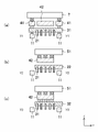
- FIG. 1 is a plan view schematically showing the overall configuration of a semiconductor integrated circuit device (semiconductor chip) according to an embodiment.
- the horizontal direction of the drawing is the X direction
- the vertical direction of the drawing is the Y direction (the same applies to subsequent figures).
- a semiconductor integrated circuit device 1 shown in FIG. 1 includes a core region 2 in which an internal core circuit is formed, and an IO region 3 provided around the core region 2 and in which an interface circuit (IO circuit) is formed.
- An IO cell row 5 is provided in the IO region 3 so as to surround the core region 2 in the peripheral portion of the semiconductor integrated circuit device 1 .
- the IO cell column 5 includes a plurality of IO cells 10 forming an interface circuit.
- the IO cell 10 includes a signal IO cell for inputting, outputting or inputting/outputting a signal, a power supply IO cell for supplying a ground potential (power supply voltage VSS), and a power supply (power supply voltage VSS) mainly for the IO area 3.
- VDDIO is 1.8V.
- an IO cell 10A for signal input/output is arranged on the upper side of the core region 2 in the drawing, and an IO cell 10B for signal input/output is arranged on the left side of the core region 2 in the drawing.
- the IO area 3 is provided with power supply wirings 6 and 7 extending in the direction in which the IO cells 10 are arranged.
- the power supply wirings 6 and 7 are formed in a ring shape on the periphery of the semiconductor integrated circuit device 1 (also called ring power supply wiring).
- the power wiring 6 supplies VDDIO
- the power wiring 7 supplies VSS.
- the semiconductor integrated circuit device 1 is provided with a plurality of external connection pads.
- FIG. 2 is a simplified configuration diagram of the IO cells 10A and 10B.
- the IO cell 10A has power supply wirings 6 and 7 extending in the X direction.
- an N conductivity type output transistor section 101 is provided under the power supply line 7 and a P conductivity type output transistor section 102 is provided under the power supply line 6 .
- the N-conductivity type output transistor section 101 and the P-conductivity type output transistor section 102 are provided outside the chip in the IO cell 10A.
- power supply wirings 6 and 7 extending in the Y direction are arranged in the IO cell 10B.
- an N conductivity type output transistor section 103 is provided under the power supply line 7 and a P conductivity type output transistor section 104 is provided under the power supply line 6 .
- the N-conductivity type output transistor section 103 and the P-conductivity type output transistor section 104 are provided outside the chip in the IO cell 10B.
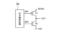
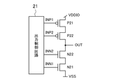
- FIG. 3 is a circuit diagram of the output circuit in this embodiment.
- a P-conductivity type (hereinafter referred to as P-type) transistor P1 is provided between a power supply VDDIO and an output terminal (which outputs an output signal OUT).
- a transistor N1 of N-conductivity type (hereinafter referred to as N-type as appropriate) is provided between it and the signal line.
- the output control circuit 20 outputs output control signals INP and INN.
- the transistor P1 receives an output control signal INP at its gate, and the transistor N1 receives an output control signal INN at its gate.
- An output signal OUT is supplied to an external connection pad.
- the output control signals INP and INN are at low level, the output signal OUT is at high level (VDDIO), and when the output control signals INP and INN are at high level, the output signal OUT is at low level (VSS).
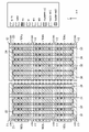
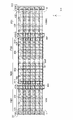
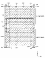
- FIG. 4 is a plan view showing the layout of the output transistor section in the IO cell 10B shown in FIG. 2(b) in this embodiment.
- 5 and 6 are plan views showing FIG. 4 divided into layers, FIG. 5 showing the configuration of the local wiring and lower layers, and FIG. 6 showing the configuration of the local wiring and higher layers.
- show. 7A and 7B are cross-sectional views showing the cross-sectional structure of the layout of FIG. The cross-sectional structure of Y3' is shown.
- the left portion of the drawing corresponds to the N conductivity type output transistor section 103 forming the transistor N1, and the right portion of the drawing corresponds to the P conductivity type output transistor section 104 forming the transistor P1.
- Fin FETs Field Effect Transistors
- the power wirings 6 and 7 shown in FIG. 2B are formed in the M2 wiring layer.
- the power supply wiring 7 for supplying VSS is provided on the N-conductivity type output transistor section 103
- the power supply wiring 6 for supplying VDDIO is provided on the P-conductivity type output transistor section 104 .
- the N conductivity type output transistor section 103 has three sections 103a, 103b, and 103c each having five fins 21 extending in parallel in the X direction.
- Embedded power supply wirings 11 extending in the X direction are arranged above and below the portions 103a, 103b, and 103c.
- the embedded power supply wiring 11 supplies VSS.
- a gate line 22 extending in the Y direction is arranged over portions 103a, 103b and 103c.
- a FinFET is formed by the Fin 21 and the gate wiring 22 .
- a local wiring 31 extending in the Y direction is commonly connected to the terminals of the fins 21 serving as the sources of the FinFETs.
- the local wiring 31 is connected to the embedded power supply wiring 11 through vias, and supplies VSS to the source of the FinFET.
- a local wiring 32 extending in the Y direction is commonly connected to terminals of the fins 21 serving as drains of the FinFETs.
- the local wiring 31 is connected via vias to the M1 wiring 41 extending in the X direction.
- the M1 wiring 41 is arranged at a position overlapping the embedded power supply wiring 11 in plan view.
- the M1 wiring 41 is connected via a via to the power supply wiring 7 formed in the M2 wiring layer.
- the local wiring 32 is connected via a via to the M1 wiring 42 extending in the X direction.
- the M1 wiring 42 is connected to the M2 wiring 51 via vias.
- the M1 wiring 42 and the M2 wiring 51 correspond to output wirings.
- the M2 wiring 51 is connected to an upper layer pad electrode (not shown).
- the configuration of the P-conductivity type output transistor section 104 is also substantially the same as that of the N-conductivity type output transistor section 103 .
- the P conductivity type output transistor section 104 has three sections 104a, 104b and 104c each having five fins 23 extending in parallel in the Y direction.
- Embedded power supply wirings 12 extending in the X direction are arranged above and below the portions 104a, 104b, and 104c in the drawing.
- the embedded power wiring 12 supplies VDDIO.
- a gate line 24 extending in the Y direction is arranged across portions 104a, 104b and 104c.
- a FinFET is formed by the Fin 23 and the gate wiring 24 .
- a local wiring 33 extending in the Y direction is commonly connected to the terminals of the fins 23 serving as the sources of the FinFETs.
- the local wiring 33 is connected to the embedded power supply wiring 12 via vias and supplies VDDIO to the source of the FinFET.
- a local wiring 34 extending in the Y direction is commonly connected to terminals of the fins 23 serving as drains of the FinFETs.
- the local wiring 33 is connected via vias to the M1 wiring 43 extending in the X direction.
- the M1 wiring 43 is arranged at a position overlapping the embedded power supply wiring 12 in plan view.
- the M1 wiring 43 is connected via a via to the power supply wiring 6 formed in the M2 wiring layer.
- the local wiring 34 is connected to the M1 wiring 42 extending in the X direction via vias.
- the power supply wiring for supplying VSS the power supply wiring 11 is formed in the embedded wiring layer, the power supply wiring 41 is formed in the M1 wiring layer, and the power supply wiring 7 is formed in the M2 wiring layer. .
- the resistance value of the VSS supply path is lowered, so that the power supply wirings 7 and 41 can be thinned.
- the power supply wirings for supplying VDDIO the power supply wiring 12 is formed in the embedded wiring layer, the power supply wiring 43 is formed in the M1 wiring layer, and the power supply wiring 6 is formed in the M2 wiring layer.
- the resistance value of the VDDIO supply path is lowered, so that the power supply wirings 6 and 43 can be thinned.
- the output wiring 42 of the M1 wiring layer and the output wiring 51 of the M2 wiring layer can be thickened while suppressing an increase in the area of the output circuit. Therefore, a large current can flow through the output terminal.
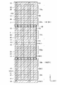
- FIG. 8 is a plan view showing the layout of the output transistor section in the IO cell 10A shown in FIG. 2(a). Note that the cross-sectional structure can be easily analogized from FIG. 7, and the illustration is omitted here.
- the upper portion of the drawing corresponds to the N conductivity type output transistor section 101 forming the transistor N1, and the lower portion of the drawing corresponds to the P conductivity type output transistor section 102 forming the transistor P1.
- Fin FETs are formed in the N conductivity type output transistor section 101 and the P conductivity type output transistor section 102 .
- the power wirings 6 and 7 shown in FIG. 2A are formed in the M1 wiring layer.
- the power supply wiring 7 for supplying VSS is provided on the N-conductivity type output transistor section 101
- the power supply wiring 6 for supplying VDDIO is provided on the P-conductivity type output transistor section 102 .
- the N conductivity type output transistor section 101 has three sections 101a, 101b, and 101c each having five fins 21 extending in parallel in the X direction.
- Embedded power supply wirings 13 extending in the X direction are arranged above and below the portions 101a, 101b, and 101c.
- the embedded power supply wiring 13 supplies VSS.
- a gate line 22 extending in the Y direction is arranged over portions 101a, 101b and 101c.
- a FinFET is formed by the Fin 21 and the gate wiring 22 .
- a local wiring 35 extending in the Y direction is commonly connected to the terminal of the fin 21 serving as the source of the FinFET.
- the local wiring 35 is connected to the embedded power supply wiring 13 through vias, and supplies VSS to the source of the FinFET.
- the local wiring 35 corresponds to power supply wiring.
- the local wiring 35 is connected via a via to the power supply wiring 7 formed in the M1 wiring layer.
- the P-conductivity type output transistor section 102 has three sections 102a, 102b, and 102c in which five fins 23 extending in parallel in the X direction are arranged.
- Embedded power supply wirings 14 extending in the X direction are arranged above and below the portions 102a, 102b, and 102c.
- the embedded power supply wiring 14 supplies VDDIO.
- a gate line 24 extending in the Y direction is arranged across portions 102a, 102b and 102c.
- a FinFET is formed by the Fin 23 and the gate wiring 24 .
- a local wiring 37 extending in the Y direction is commonly connected to the terminals of the fins 23 serving as the sources of the FinFETs.
- the local wiring 37 is connected to the embedded power supply wiring 14 via vias and supplies VDDIO to the source of the FinFET.
- the local wiring 37 corresponds to power supply wiring.
- the local wiring 37 is connected via vias to the power supply wiring 6 formed in the M1 wiring layer.
- a terminal of the fin 21 serving as the drain of the FinFET in the N-conductivity output transistor section 101 and a terminal of the fin 23 serving as the drain of the FinFET in the P-conductivity output transistor section 102 share a local wiring 36 extending in the Y direction. It is connected to the.
- the local wiring 36 is connected to the M1 wiring 45 via vias. Local wiring 36 and M1 wiring 45 correspond to output wiring.
- the M1 wiring 45 is connected to an upper layer pad electrode (not shown).
- the power supply wiring 13 is formed in the embedded wiring layer, the local wiring 35 is formed, and the power supply wiring 7 is formed in the M1 wiring layer as the power supply wiring for supplying VSS.
- the resistance value of the VSS supply path is lowered, so that the power supply wiring 7 can be thinned.
- the power supply wiring 14 is formed in the embedded wiring layer, the local wiring 37 is formed, and the power supply wiring 6 is formed in the M1 wiring layer.
- the resistance value of the VDDIO supply path is reduced, so that the power supply wiring 6 can be thinned.
- the output wiring 45 of the M1 wiring layer can be thickened while suppressing an increase in the area of the output circuit. Therefore, a large current can flow through the output terminal.
- an embedded power supply wiring 13 supplying VSS and an embedded power supply wiring 14 supplying VDDIO are formed between the transistor N1 and the transistor P1. Since the embedded power supply wiring is formed by embedding metal wiring in grooves provided in the substrate, wells in the substrate, STI, etc., it has the effect of reducing noise propagation through the substrate and the like. Therefore, by providing a buried power supply wiring between transistors N1 and P1, latch-up resistance can be improved.
- FIG. 9 is a circuit diagram of an output circuit in a modification.
- P-type transistors P21 and P22 are provided in series between the power supply VDDIO and the output signal line, and N-type transistors N21 and P22 are provided between the power supply VSS and the output signal line. N22 are arranged in series.
- the output control circuit 21 outputs output control signals INP1, INP2, INN1 and INN2.
- Transistor P21 receives output control signal INP1 at its gate, and transistor P22 receives output control signal INP2 at its gate.
- Transistor N21 receives output control signal INN1 at its gate, and transistor N22 receives output control signal INN2 at its gate.
- the output signal OUT is then supplied to an external connection pad.
- the output control signals INP1, INP2, INN1 and INN2 are at low level, the output signal OUT is at high level (VDDIO), and when the output control signals INP1, INP2, INN1 and INN2 are at high level, the output signal OUT is at low level. (VSS).
- One of the output control signals INP1 and INP2 may be at the fixed potential (VSS) and one of the output control signals INN1 and INN2 may be at the fixed potential (VDDIO).
- FIG. 10 is a plan view showing the layout of the output transistor section in the IO cell 10B shown in FIG. 2(b) according to this modification.
- the left portion of the drawing corresponds to the N conductivity type output transistor section 103 that constitutes the transistors N21 and N22
- the right portion of the drawing corresponds to the P conductivity type output transistor section 104 that constitutes the transistors P21 and P22. do.
- Fin FETs are formed in the N conductivity type output transistor section 103 and the P conductivity type output transistor section 104 .
- the power wirings 6 and 7 shown in FIG. 2B are formed in the M2 wiring layer.
- the power supply wiring 7 for supplying VSS is provided on the N-conductivity type output transistor section 103
- the power supply wiring 6 for supplying VDDIO is provided on the P-conductivity type output transistor section 104 .
- the layout of FIG. 10 has a longer fin length because the transistors are arranged in series in two stages, and two gate wirings are arranged between the local wirings.
- the basic configuration is the same as that of the above-described embodiment, and detailed description will be omitted.
- the M1 wiring 44 is connected to the M2 wiring 52, and the M2 wiring 52 is connected to an upper layer pad electrode (not shown).
- FIG. 11 is a plan view showing the layout of the output transistor section in the IO cell 10A shown in FIG. 2(a) in this modification.
- the upper portion of the drawing corresponds to the N conductivity type output transistor section 101 forming the transistors N21 and N22
- the lower portion of the drawing corresponds to the P conductivity type output transistor section 102 forming the transistors P21 and P22.
- Fin FETs are formed in the N conductivity type output transistor section 101 and the P conductivity type output transistor section 102 .
- the power wirings 6 and 7 shown in FIG. 2B are formed in the M1 wiring layer.
- the power supply wiring 7 for supplying VSS is provided on the N-conductivity type output transistor section 101
- the power supply wiring 6 for supplying VDDIO is provided on the P-conductivity type output transistor section 102 .
- the layout of FIG. 11 has two tiers of transistors in series, so the length of the fin is longer, and two gate wirings are arranged between the local wirings.
- the basic configuration is the same as that of the above-described embodiment, and detailed description will be omitted.
- the M1 wiring 46 is connected to an upper layer pad electrode (not shown).
- the same effects as those of the above-described embodiment can be obtained. That is, in the layout of FIG. 10, the output wiring 44 of the M1 wiring layer and the output wiring 52 of the M2 wiring layer can be thickened while suppressing an increase in the area of the output circuit. Therefore, a large current can flow through the output terminal. In the layout of FIG. 11, the output wiring 46 of the M1 wiring layer can be thickened while suppressing an increase in the area of the output circuit. Therefore, a large current can flow through the output terminal.
- an embedded power supply wiring for supplying VSS and an embedded power supply wiring for supplying VDDIO are formed between the transistor N1 and the transistor P1. Since the embedded power supply wiring is formed by embedding metal wiring in grooves provided in the substrate, wells in the substrate, STI, etc., it has the effect of reducing noise propagation through the substrate and the like. Therefore, by providing a buried power supply wiring between transistors N1 and P1, latch-up resistance can be improved.
- FIG. 12 is a diagram showing the overall configuration of a semiconductor integrated circuit device according to the second embodiment.
- a semiconductor integrated circuit device 200 is configured by stacking a first semiconductor chip 201 (chip A) and a second semiconductor chip 202 (chip B). In the stacked portion, the back surface of the first semiconductor chip 201 and the main surface of the second semiconductor chip 202 face each other.
- the first semiconductor chip 201 is formed with a circuit including a transistor that constitutes an output buffer, and is also formed with an embedded power supply wiring.
- the second semiconductor chip 202 has power supply wirings connected to embedded power supply wirings formed in the first semiconductor chip 201 .
- the embedded power wiring formed in the first semiconductor chip 201 and the power wiring formed in the second semiconductor chip 202 are connected via a through silicon via (TSV).
- TSV through silicon via
- the plan view of the semiconductor integrated circuit device 200 shown in FIG. 12 is the same as in FIG. That is, the first semiconductor chip 201 includes a core region 2 in which an internal core circuit is formed, and an IO region 3 provided around the core region 2 and in which an interface circuit (IO circuit) is formed.
- An IO cell array 5 is provided in the IO region 3 so as to surround the core region 2 in the peripheral portion of the semiconductor integrated circuit device 200 .
- a plurality of IO cells 10 forming an interface circuit are arranged in the IO cell column 5 .
- the power wirings 6 and 7 extending in the direction in which the IO cells 10 are arranged are formed on the second semiconductor chip 202 .
- the simple configuration of the IO cells 10A and 10B is the same as in FIG. 2, and the circuit diagram of the output circuit is the same as in FIG.
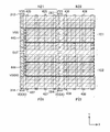
- FIG. 13 is a plan view showing the layout of the output transistor section in the IO cell 10B shown in FIG. 2(b) in this embodiment.
- the layout of FIG. 13 corresponds to the circuit diagram of FIG. 14 to 16 are plan views showing FIG. 13 divided into layers.
- 14 shows the configuration of the power supply wiring of the second semiconductor chip 202 and the embedded power supply wiring and fins of the first semiconductor chip 201
- FIG. FIG. 16 shows the configuration of the local wiring of the first semiconductor chip 201 and the upper layers.
- 17A and 17B are cross-sectional views showing the cross-sectional structure of the layout of FIG. The cross-sectional structure of Y3' is shown.
- the left portion of the drawing corresponds to the N conductivity type output transistor portion 103 forming the transistor N1, and the right portion of the drawing corresponds to the P conductivity type output transistor portion 104 forming the transistor P1.
- Fin FETs Field Effect Transistors
- the power wirings 6 and 7 shown in FIG. 2B are formed on the second semiconductor chip 202 .
- the power supply wiring 7 for supplying VSS is provided at a position overlapping with the N-conductivity type output transistor section 103 in plan view
- the power supply wiring 6 for supplying VDDIO is provided at a position overlapping with the P-conductivity type output transistor section 104 in plan view. It is
- the N conductivity type output transistor section 103 has three sections 103a, 103b, and 103c each having five fins 21 extending in parallel in the X direction.
- Embedded power supply wirings 11 extending in the X direction are arranged above and below the portions 103a, 103b, and 103c in the drawing.
- the embedded power supply wiring 11 supplies VSS.
- the embedded power supply wiring 11 is connected to the power supply wiring 7 of the second semiconductor chip 202 via the TSV.
- a gate wiring 22 extending in the Y direction is arranged over the portions 103a, 103b, and 103c.
- a FinFET is formed by the Fin 21 and the gate wiring 22 .
- a local wiring 31 extending in the Y direction is commonly connected to the terminal of the fin 21 serving as the source of the FinFET.
- the local wiring 31 is connected to the embedded power supply wiring 11 through vias, and supplies VSS to the source of the FinFET.
- a local wiring 32 extending in the Y direction is commonly connected to terminals of the fins 21 serving as drains of the FinFETs.
- the local wiring 32 is connected via a via to the M1 wiring 242 extending in the X direction.
- the M1 wiring 242 is connected to the M2 wiring 251 through vias 261 .
- the M1 wiring 242 and the M2 wiring 251 correspond to output wirings.
- the M2 wiring 251 is connected to an upper layer pad electrode (not shown).
- the P-conductivity type output transistor section 104 has three sections 104a, 104b, and 104c each having five fins 23 extending in parallel in the X direction.
- Embedded power supply wirings 12 extending in the X direction are arranged above and below the portions 104a, 104b, and 104c in the drawing.
- the embedded power wiring 12 supplies VDDIO.
- the embedded power wiring 12 is connected to the power wiring 6 of the second semiconductor chip 202 via the TSV.
- a gate wiring 24 extending in the Y direction is arranged over the portions 104a, 104b, and 104c.
- a FinFET is formed by the Fin 23 and the gate wiring 24 .
- a local wiring 33 extending in the Y direction is commonly connected to the terminals of the fins 23 serving as the sources of the FinFETs.
- the local wiring 33 is connected to the embedded power supply wiring 12 via vias and supplies VDDIO to the source of the FinFET.
- a local wiring 34 extending in the Y direction is commonly connected to terminals of the fins 23 serving as drains of the FinFETs.
- the local wiring 34 is connected via a via to the M1 wiring 242 extending in the X direction.
- the power wirings 6 and 7 of the second semiconductor chip 202 overlap the M2 wirings 251 of the first semiconductor chip 201 in plan view. Also, the arrangement position of the via 261 connecting the M1 wiring 242 and the M2 wiring 251 overlaps with the power supply wirings 6 and 7 of the second semiconductor chip 202 in plan view.
- the power wiring 11 formed in the embedded wiring layer of the first semiconductor chip 201 and the power wiring 7 formed in the second semiconductor chip 202 are formed as power wiring for supplying VSS. ing.
- the resistance value of the VSS supply path can be reduced without providing the power wiring in the M1 wiring layer of the first semiconductor chip 201 .
- power supply wirings for supplying VDDIO power supply wirings 12 formed in the embedded wiring layer of the first semiconductor chip 201 and power supply wirings 6 formed in the second semiconductor chip 202 are formed.
- the resistance value of the VDDIO supply path can be reduced without providing the power wiring in the M1 wiring layer of the first semiconductor chip 201 .
- the output wiring 242 of the M1 wiring layer and the output wiring 251 of the M2 wiring layer can be thickened, and the number of vias 261 connecting them can be increased.
- a large current can flow through the
- the power supply wirings 6 and 7 formed on the second semiconductor chip 202 also overlap the output wiring 251 in a plan view, and can be made thicker.
- FIG. 18 is a plan view showing the layout of the output transistor section in the IO cell 10A shown in FIG. 2(a) in this embodiment. Note that the cross-sectional structure can be easily analogized from FIG. 17, and the illustration is omitted here.
- the upper portion of the drawing corresponds to the N conductivity type output transistor section 101 forming the transistor N1, and the lower portion of the drawing corresponds to the P conductivity type output transistor section 102 forming the transistor P1.
- Fin FETs are formed in the N conductivity type output transistor section 101 and the P conductivity type output transistor section 102 .
- the power wirings 6 and 7 shown in FIG. 2A are formed on the second semiconductor chip 202 .
- the power wiring 7 for supplying VSS is provided at a position overlapping with the N-conductivity type output transistor section 101 in plan view
- the power wiring 6 for supplying VDDIO is provided at a position overlapping with the P-conductivity type output transistor section 102 in plan view. It is
- the N conductivity type output transistor section 101 has three sections 101a, 101b, and 101c each having five fins 21 extending in parallel in the X direction.
- Embedded power supply wirings 13 extending in the X direction are arranged above and below the portions 101a, 101b, and 101c in the drawing.
- the embedded power supply wiring 13 supplies VSS.
- the embedded power supply wiring 13 is connected to the power supply wiring 7 of the second semiconductor chip 202 via the TSV.
- a gate wiring 22 extending in the Y direction is arranged over the portions 101a, 101b, and 101c.
- a FinFET is formed by the Fin 21 and the gate wiring 22 .
- a local wiring 35 extending in the Y direction is commonly connected to the terminals of the fins 21 serving as the sources of the FinFETs.
- the local wiring 35 is connected to the embedded power supply wiring 13 through vias, and supplies VSS to the source of the FinFET.
- the P-conductivity type output transistor section 102 has three sections 102a, 102b, and 102c in which five fins 23 extending in parallel in the X direction are arranged.
- Embedded power supply wirings 14 extending in the X direction are arranged above and below the portions 102a, 102b, and 102c in the drawing.
- the embedded power supply wiring 14 supplies VDDIO.
- the embedded power supply wiring 14 is connected to the power supply wiring 6 of the second semiconductor chip 202 via the TSV.
- a gate wiring 24 extending in the Y direction is arranged over the portions 102a, 102b, and 102c.
- a FinFET is formed by the Fin 23 and the gate wiring 24 .
- a local wiring 37 extending in the Y direction is commonly connected to the terminals of the fins 23 serving as the sources of the FinFETs.
- the local wiring 37 is connected to the embedded power supply wiring 14 via vias and supplies VDDIO to the source of the FinFET.
- a terminal of the fin 21 serving as the drain of the FinFET in the N-conductivity output transistor section 101 and a terminal of the fin 23 serving as the drain of the FinFET in the P-conductivity output transistor section 102 share a local wiring 36 extending in the Y direction. It is connected to the. Local wiring 36 is connected to M1 wiring 245 via via 262 . Local wiring 36 and M1 wiring 245 correspond to output wiring. The M1 wiring 245 is connected to an upper layer pad electrode (not shown).
- the power wirings 6 and 7 of the second semiconductor chip 202 overlap the M1 wirings 245 of the first semiconductor chip 201 in plan view. Also, the arrangement position of the via 262 connecting the local wiring 36 and the M1 wiring 245 overlaps with the power supply wirings 6 and 7 of the second semiconductor chip 202 in plan view.
- the power wiring 13 formed in the embedded wiring layer of the first semiconductor chip 201 and the power wiring 7 formed in the second semiconductor chip 202 are formed as the power wiring for supplying VSS. ing.
- the resistance value of the VSS supply path can be lowered without providing the power wiring in the M1 wiring layer of the first semiconductor chip 201 .
- the power supply wirings 14 formed in the embedded wiring layer of the first semiconductor chip 201 and the power supply wirings 6 formed in the second semiconductor chip 202 are formed.
- the resistance value of the VDDIO supply path can be reduced without providing the power wiring in the M1 wiring layer of the first semiconductor chip 201 .
- the output wiring 245 of the M1 wiring layer can be thickened, and the number of vias 262 for connecting to the local wiring 36 can be increased, so that a large current can flow to the output terminal. can flow.
- the power supply wirings 6 and 7 formed on the second semiconductor chip 202 also overlap the output wiring 245 in a plan view, and can be made thicker.
- the power supply wirings 6 and 7 formed on the second semiconductor chip 202 may be of a single layer or may be of multiple layers.
- the wiring direction is not limited to the one shown here.
- each layer may be extended in a direction perpendicular to each other to form a mesh-like power wiring. This makes it possible to further strengthen the power supply.
- both the VSS power supply wiring and the VDDIO power supply wiring are formed on the second semiconductor chip 202, but only one of the power supply wirings may be formed on the second semiconductor chip 202. .
- the output transistor has a two-stage configuration, it can be similarly configured.
- the BPR that is, the power supply wiring formed in the embedded wiring layer extends in the X direction.
- the BPR extends in the Y direction.
- Configuration example 1 corresponds to the first embodiment.
- the circuit configuration of the output circuit is as shown in the circuit diagram of FIG.
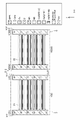
- FIG. 19 is a plan view showing the layout of the output transistor section in the IO cell 10B shown in FIG. 2(b) in this configuration example.
- 20 and 21 are plan views showing FIG. 19 divided into layers, FIG. 20 showing the configuration of the local wiring and lower layers, and FIG. 21 showing the configuration of the local wiring and higher layers.
- show. 19 to 21 are diagrams corresponding to FIGS. 4 to 6 shown in the first embodiment, and explanations of configurations that can be easily guessed from the description of the first embodiment may be omitted.
- the left portion of the drawing corresponds to the N conductivity type output transistor portion 103 forming the transistor N1, and the right portion of the drawing corresponds to the P conductivity type output transistor portion 104 forming the transistor P1.
- Fin FETs Field Effect Transistors
- the power wirings 6 and 7 shown in FIG. 2B are formed in the M2 wiring layer.
- the power supply wiring 7 for supplying VSS is provided on the N-conductivity type output transistor section 103
- the power supply wiring 6 for supplying VDDIO is provided on the P-conductivity type output transistor section 104 .
- an output wiring 51 is formed in the M2 wiring layer.
- the M2 wiring 51 is connected to an upper layer pad electrode (not shown).
- the N conductivity type output transistor section 103 has ten fins 21 extending in parallel in the X direction.
- Embedded power supply wirings 311 extending in the Y direction are arranged on the left and right sides of the fin 21 in the drawing, respectively.
- the embedded power supply wiring 311 supplies VSS.
- a gate wiring 22 extending in the Y direction over ten fins 21 is arranged.
- a FinFET is formed by the Fin 21 and the gate wiring 22 .
- a local wiring 330 extending in the Y direction is formed in a layer above the embedded power supply wiring 311 so as to overlap the embedded power supply wiring 311 in a plan view.
- the local wiring 330 is connected to the underlying embedded power supply wiring 311 via vias.
- a local wiring 331 extending in the Y direction is commonly connected to the terminal of the fin 21 serving as the source of the FinFET.
- the local wiring 331 is connected to the local wiring 330 via five M1 wirings 341 extending in parallel in the X direction, and supplies VSS to the source of the FinFET.
- the M1 wiring 341 is connected via vias to the power supply wiring 7 formed in the M2 wiring layer.
- a local wiring 332 extending in the Y direction is commonly connected to the terminals of the fins 21 serving as the drains of the finFETs.
- the local wiring 332 is connected via a via to the M1 wiring 342 extending in parallel in the X direction.
- the M1 wiring 342 is connected to the M2 wiring 51 via vias.
- the configuration of the P-conductivity type output transistor section 104 is also substantially the same as that of the N-conductivity type output transistor section 103 .
- Ten fins 23 extending in parallel in the X direction are arranged in the P conductivity type output transistor section 104 .
- Embedded power supply wirings 312 extending in the Y direction are arranged on the left and right sides of the fin 23 in the drawing, respectively.
- the embedded power wiring 312 supplies VDDIO.
- a gate wiring 24 extending in the Y direction over ten fins 23 is arranged.
- a FinFET is formed by the Fin 23 and the gate wiring 24 .
- a local wiring 335 extending in the Y direction is formed on the upper layer of the embedded power supply wiring 312 so as to overlap with the embedded power supply wiring 312 in plan view.
- the local wiring 335 is connected to the underlying embedded power supply wiring 312 via vias.
- a local wiring 333 extending in the Y direction is commonly connected to the terminals of the fins 23 serving as the sources of the FinFETs.
- the local wiring 333 is connected to the local wiring 335 via five M1 wirings 343 extending in parallel in the X direction, and supplies VDDIO to the source of the FinFET.
- the M1 wiring 343 is connected via a via to the power supply wiring 6 formed in the M2 wiring layer.
- a local wiring 334 extending in the Y direction is commonly connected to the terminals of the fins 23 serving as the drains of the finFETs. Similar to the local wiring 332, the local wiring 334 is connected via vias to five M1 wirings 342 extending in parallel in the X direction.
- the power supply wiring for supplying VSS the power supply wiring 311 is formed in the embedded wiring layer, the local wiring 330 is formed, the power supply wiring 341 is formed in the M1 wiring layer, and the power supply wiring is formed in the M2 wiring layer.
- a wiring 7 is formed.
- the resistance value of the VSS supply path is lowered, so that the power supply wiring 7 can be thinned.
- a power supply wiring 312 is formed in the embedded wiring layer, a local wiring 335 is formed, a power supply wiring 343 is formed in the M1 wiring layer, and a power supply wiring 6 is formed in the M2 wiring layer.
- the resistance value of the VDDIO supply path is reduced, so that the power supply wiring 6 can be thinned.
- the output wiring 51 of the M2 wiring layer can be thickened while suppressing an increase in the area of the output circuit. Therefore, a large current can flow through the output terminal.
- an embedded power supply wiring 311 supplying VSS and an embedded power supply wiring 312 supplying VDDIO are formed between the transistor N1 and the transistor P1. Since the embedded power supply wiring is formed by embedding metal wiring in grooves provided in the substrate, wells in the substrate, STI, etc., it has the effect of reducing noise propagation through the substrate and the like. Therefore, by providing embedded power supply wirings 311 and 312 between transistors N1 and P1, latch-up resistance can be improved.
- FIG. 22 is a plan view showing the layout of the output transistor section in the IO cell 10A shown in FIG. 2(a) in this configuration example.
- FIG. 22 is a diagram corresponding to FIG. 8 shown in the first embodiment, and the description of the configuration that can be easily guessed from the description of the first embodiment may be omitted.
- the upper portion of the drawing corresponds to the N conductivity type output transistor section 101 forming the transistor N1, and the lower portion of the drawing corresponds to the P conductivity type output transistor section 102 forming the transistor P1.
- Fin FETs are formed in the N conductivity type output transistor section 101 and the P conductivity type output transistor section 102 .
- the power wirings 6 and 7 shown in FIG. 2A are formed in the M1 wiring layer.
- the power supply wiring 7 for supplying VSS is provided on the N-conductivity type output transistor section 101
- the power supply wiring 6 for supplying VDDIO is provided on the P-conductivity type output transistor section 102 .
- the N conductivity type output transistor section 101 has ten fins 21 extending in parallel in the X direction.
- Embedded power supply wirings 313 extending in the Y direction are arranged on the left and right sides of the fin 21 in the drawing, respectively.
- the embedded power supply wiring 313 supplies VSS.
- a gate wiring 22 extending in the Y direction over ten fins 21 is arranged.
- a FinFET is formed by the Fin 21 and the gate wiring 22 .
- a local wiring 336 extending in the Y direction is formed on the upper layer of the embedded power supply wiring 313 so as to overlap with the embedded power supply wiring 313 in plan view.
- the local wiring 336 is connected to the underlying embedded power supply wiring 313 via vias. Also, the local wiring 336 is connected to the power supply wiring 7 formed in the upper M1 wiring layer through vias.
- a local wiring 337 extending in the Y direction is commonly connected to the terminal of the fin 21 serving as the source of the FinFET.
- the local wiring 337 is connected to the power supply wiring 7 formed in the M1 wiring layer via vias, and supplies VSS to the source of the FinFET.
- the P-type output transistor section 102 has ten fins 23 extending in parallel in the X direction.
- Embedded power supply wirings 314 extending in the Y direction are arranged on the left and right sides of the fin 23 in the drawing, respectively.
- the embedded power wiring 314 supplies VDDIO.
- a gate wiring 24 extending in the Y direction over ten fins 23 is arranged.
- a FinFET is formed by the Fin 23 and the gate wiring 24 .
- a local wiring 340 extending in the Y direction is formed in a layer above the embedded power supply wiring 314 so as to overlap the embedded power supply wiring 314 in a plan view.
- the local wiring 340 is connected to the underlying embedded power supply wiring 314 via vias. Also, the local wiring 340 is connected to the power supply wiring 6 formed in the upper M1 wiring layer through vias.
- a local wiring 338 extending in the Y direction is commonly connected to the terminals of the fins 23 serving as the sources of the FinFETs.
- the local wiring 338 is connected to the power supply wiring 6 formed in the M1 wiring layer via vias, and supplies VDDIO to the source of the FinFET.
- a local wiring 339 extending in the Y direction is common to the terminal of the fin 21 serving as the drain of the FinFET in the N-conductivity output transistor section 101 and the terminal of the fin 23 serving as the drain of the FinFET in the P-conductivity output transistor section 102 . It is connected to the.
- the local wiring 339 is connected via a via to the output wiring 45 formed in the M1 wiring layer.
- the M1 wiring 45 is connected to an upper layer pad electrode (not shown).
- the power supply wiring for supplying VSS the power supply wiring 313 is formed in the embedded wiring layer, the local wirings 336 and 337 are formed, and the power supply wiring 7 is formed in the M1 wiring layer.
- the resistance value of the VSS supply path is lowered, so that the power supply wiring 7 can be thinned.
- a power supply wiring 314 is formed in the embedded wiring layer, local wirings 338 and 340 are formed, and a power supply wiring 6 is formed in the M1 wiring layer.
- the resistance value of the VDDIO supply path is reduced, so that the power supply wiring 6 can be thinned.
- the output wiring 45 of the M1 wiring layer can be thickened while suppressing an increase in the area of the output circuit. Therefore, a large current can flow through the output terminal.
- Configuration example 2 corresponds to the circuit diagram of FIG. 9 according to the modification of the first embodiment
- Configuration example 2 corresponds to a modification of the first embodiment.
- the circuit configuration of the output circuit is as shown in the circuit diagram of FIG.
- FIG. 23 is a plan view showing the layout of the output transistor section in the IO cell 10B shown in FIG. 2(b) in this configuration example.
- 24 and 25 are plan views showing FIG. 23 divided into layers, FIG. 24 showing the configuration of the local wiring and lower layers, and FIG. 25 showing the configuration of the local wiring and higher layers.
- show. 23 to 25 are diagrams corresponding to FIG. 10 shown in the modified example of the first embodiment, and the description of the configuration that can be easily guessed from the description of the modified example of the first embodiment may be omitted. be.
- the left portion of the drawing corresponds to the N conductivity type output transistor portion 103 forming the transistors N21 and N22, and the right portion of the drawing corresponds to the P conductivity type output transistor portion forming the transistors P21 and P22.
- Fin FETs are formed in the N conductivity type output transistor section 103 and the P conductivity type output transistor section 104 .
- the power wirings 6 and 7 shown in FIG. 2B are formed in the M2 wiring layer.
- the power supply wiring 7 for supplying VSS is provided on the N-conductivity type output transistor section 103
- the power supply wiring 6 for supplying VDDIO is provided on the P-conductivity type output transistor section 104 .
- an output wiring 52 is formed in the M2 wiring layer.
- the M2 wiring 52 is connected to an upper layer pad electrode (not shown).
- the layouts of FIGS. 23 to 25 have longer fins because the transistors are arranged in series in two stages, and two gate wirings are provided between the local wirings. are placed.
- the basic configuration is the same as that of configuration example 1 described above, and detailed description thereof will be omitted.
- the output wiring 52 of the M2 wiring layer can be thickened while suppressing an increase in the area of the output circuit. Therefore, a large current can flow through the output terminal.
- FIG. 26 is a modified example of the configuration of FIG.
- the series-connected transistors N21 and N22 are configured by a single fin, and the serially-connected transistors P21 and P22 are configured by a single fin.
- the fins forming the transistor N21 and the fins forming the transistor N22 are separated, and the fins forming the transistor P21 and the fin forming the transistor P22 are separated. ing. That is, the transistor N21 and the transistor N22 are configured independently of each other, and the structures forming the channel, gate, source and drain are separated from each other. Further, the transistor P21 and the transistor P22 are configured independently of each other, and the structures forming the channel, gate, source and drain are separated from each other.
- an embedded power supply wiring 311 is formed between the transistor N21 and the transistor N22.
- a local wiring 431 connected to a terminal serving as the drain of the fin of the transistor N21 and a local wiring 432 connected to a terminal serving as the source of the fin of the transistor N22 are connected to each other. are connected via an M1 wiring 441 extending in the direction.
- an embedded power supply wiring 312 is formed between the transistor P21 and the transistor P22.
- a local wiring 433 connected to a terminal serving as the drain of the fin of the transistor P21 and a local wiring 434 connected to a terminal serving as the source of the fin of the transistor P22 are connected to each other. are connected via an M1 wiring 442 extending in the direction.
- the transistors N21 and N22 are formed by fins separated from each other, and the transistors P21 and P22 are formed by fins separated from each other. Thereby, the ESD resistance of the semiconductor integrated circuit device can be improved.
- FIG. 27 is a plan view showing the layout of the output transistor section in the IO cell 10A shown in FIG. 2(a) in this configuration example.
- FIG. 27 is a diagram corresponding to FIG. 11 showing the modified example of the first embodiment, and the description of the configuration that can be easily guessed from the description of the first embodiment may be omitted.
- the upper portion of the drawing corresponds to the N conductivity type output transistor section 101 forming the transistors N21 and N22
- the lower portion of the drawing corresponds to the P conductivity type output transistor section 102 forming the transistors P21 and P22.
- Fin FETs are formed in the N conductivity type output transistor section 101 and the P conductivity type output transistor section 102 .
- the power wirings 6 and 7 shown in FIG. 2B are formed in the M1 wiring layer.
- the power supply wiring 7 for supplying VSS is provided on the N-conductivity type output transistor section 101
- the power supply wiring 6 for supplying VDDIO is provided on the P-conductivity type output transistor section 102 .
- an output wiring 45 is formed in the M1 wiring layer.
- the output wiring 45 of the M1 wiring layer can be thickened while suppressing an increase in the area of the output circuit. Therefore, a large current can flow through the output terminal.
- FIG. 28 is a modified example of the configuration of FIG.
- the series-connected transistors N21 and N22 are configured by a series of fins
- the series-connected transistors P21 and P22 are configured by a series of fins.
- the fins forming the transistor N21 and the fins forming the transistor N22 are separated, and the fins forming the transistor P21 and the fin forming the transistor P22 are separated. ing. That is, the transistor N21 and the transistor N22 are configured independently of each other, and the structures forming the channel, gate, source and drain are separated from each other.
- the transistor P21 and the transistor P22 are configured independently of each other. The structures that make up the channel, gate, source and drain are isolated from each other.
- an embedded power supply wiring 313 is formed between the transistor N21 and the transistor N22.
- a local wiring 435 connected to a terminal serving as the drain of the fin of the transistor N21 and a local wiring 436 connected to a terminal serving as the source of the fin of the transistor N22 are connected to each other. are connected via an M1 wiring 443 extending in the direction.
- an embedded power supply wiring 314 is formed between the transistor P21 and the transistor P22. Then, a local wiring 437 connected to a terminal serving as the drain of the fin of the transistor P21 and a local wiring 438 connected to a terminal serving as the source of the fin of the transistor P22 are connected to each other. are connected via an M1 wiring 444 extending in the direction.
- the transistors N21 and N22 are formed by fins separated from each other, and the transistors P21 and P22 are formed by fins separated from each other. Thereby, the ESD resistance of the semiconductor integrated circuit device can be improved.
- Configuration example 3 corresponds to the above-described second embodiment.
- the overall configuration of the semiconductor integrated circuit device is as shown in FIG. 12, and the circuit configuration of the output circuit is as shown in the circuit diagram of FIG.
- FIG. 29 is a plan view showing the layout of the output transistor section in the IO cell 10B shown in FIG. 2(b) in the third configuration example.
- the layout of FIG. 29 corresponds to the circuit diagram of FIG. 30 to 32 are plan views showing FIG. 29 divided into layers.
- 30 shows the configuration of the power supply wiring of the second semiconductor chip 202 and the embedded power supply wiring and fins of the first semiconductor chip 201
- FIG. FIG. 32 shows the configuration of the local wiring of the first semiconductor chip 201 and the upper layers.
- 29 to 32 are diagrams corresponding to FIGS. 13 to 16 shown in the second embodiment, and explanations of configurations that can be easily guessed from the description of the second embodiment may be omitted.
- the left portion of the drawing corresponds to the N conductivity type output transistor portion 103 forming the transistor N1
- the right portion of the drawing corresponds to the P conductivity type output transistor portion 104 forming the transistor P1.
- Fin FETs Field Effect Transistors
- the power wirings 6 and 7 shown in FIG. 2B are formed on the second semiconductor chip 202 .
- the power supply wiring 7 for supplying VSS is provided at a position overlapping with the N-conductivity type output transistor section 103 in plan view, and the power supply wiring 6 for supplying VDDIO is provided at a position overlapping with the P-conductivity type output transistor section 104 in plan view. It is
- the N conductivity type output transistor section 103 has ten fins 21 extending in parallel in the X direction.
- Embedded power supply wirings 511 extending in the Y direction are arranged on the left and right sides of the fin 21 in the drawing.
- An embedded power supply wiring 511 supplies VSS.
- the embedded power wiring 511 is connected to the power wiring 7 of the second semiconductor chip 202 via the TSV.
- a gate wiring 22 extending in the Y direction over ten fins 21 is arranged.
- a FinFET is formed by the Fin 21 and the gate wiring 22 .
- a local wiring 530 extending in the Y direction is formed on the upper layer of the embedded power supply wiring 511 so as to overlap with the embedded power supply wiring 511 in plan view.
- the local wiring 530 is connected to the underlying embedded power supply wiring 511 via vias.
- a local wiring 531 extending in the Y direction is commonly connected to the terminals of the fins 21 serving as the sources of the FinFETs.
- the local wiring 531 is connected to the local wiring 530 via the M1 wiring 541 extending in the X direction, and supplies VSS to the source of the FinFET.
- a local wiring 532 extending in the Y direction is commonly connected to the terminals of the fins 21 serving as the drains of the finFETs.
- the local wiring 532 is connected via a via to the M1 wiring 542 extending in the X direction.
- the M1 wiring 542 is connected to the M2 wiring 551 through vias 561 .
- the M1 wiring 542 and the M2 wiring 551 correspond to output wirings.
- the M2 wiring 551 is connected to an upper layer pad electrode (not shown).
- the P-conductivity type output transistor section 104 has ten fins 23 extending in parallel in the X direction.
- Embedded power supply wirings 512 extending in the Y direction are arranged on the left and right sides of the fin 23 in the drawing.
- the embedded power supply wiring 512 supplies VDDIO.
- the embedded power supply wiring 512 is connected to the power supply wiring 6 of the second semiconductor chip 202 via the TSV.
- a gate wiring 24 extending in the Y direction over ten fins 23 is arranged.
- a FinFET is formed by the Fin 23 and the gate wiring 24 .
- a local wiring 535 extending in the Y direction is formed in a layer above the embedded power supply wiring 512 so as to overlap the embedded power supply wiring 512 in plan view.
- the local wiring 535 is connected to the underlying embedded power supply wiring 512 via vias.
- a local wiring 533 extending in the Y direction is commonly connected to the terminal of the fin 23 serving as the source of the FinFET.
- the local wiring 533 is connected to the local wiring 535 via the M1 wiring 543 extending in the X direction, and supplies VDDIO to the source of the FinFET.
- a local wiring 534 extending in the Y direction is commonly connected to the terminals of the fins 23 serving as the drains of the finFETs.
- the local wiring 534 is connected via a via to the M1 wiring 542 extending in the X direction.
- the power wirings 6 and 7 of the second semiconductor chip 202 overlap the M2 wirings 551 of the first semiconductor chip 201 in plan view. Also, the arrangement position of the via 561 connecting the M1 wiring 542 and the M2 wiring 551 overlaps with the power supply wirings 6 and 7 of the second semiconductor chip 202 in plan view.
- the power wiring 511 formed in the embedded wiring layer of the first semiconductor chip 201 and the power wiring 7 formed in the second semiconductor chip 202 are formed as the power wiring for supplying VSS. ing.
- the resistance value of the VSS supply path can be reduced even if the number of power supply wirings in the M1 wiring layer of the first semiconductor chip 201 is reduced.
- power supply wirings for supplying VDDIO power supply wirings 512 formed in the embedded wiring layer of the first semiconductor chip 201 and power supply wirings 6 formed in the second semiconductor chip 202 are formed.
- the resistance value of the VDDIO supply path can be reduced even if the power wiring of the M1 wiring layer of the first semiconductor chip 201 is reduced.
- the output wiring 542 of the M1 wiring layer and the output wiring 551 of the M2 wiring layer can be thickened, and the number of vias 561 connecting them can be increased.
- a large current can flow through the
- the power supply wirings 6 and 7 formed on the second semiconductor chip 202 also overlap the output wiring 551 in a plan view, and can be made thicker.
- an embedded power supply wiring 511 supplying VSS and an embedded power supply wiring 512 supplying VDDIO are formed between the transistor N1 and the transistor P1. Since the embedded power supply wiring is formed by embedding metal wiring in grooves provided in the substrate, wells in the substrate, STI, etc., it has the effect of reducing noise propagation through the substrate and the like. Therefore, by providing a buried power supply wiring between transistors N1 and P1, latch-up resistance can be improved.
- FIG. 33 is a plan view showing the layout of the output transistor section in the IO cell 10A shown in FIG. 2(a) in the third configuration example.
- FIG. 33 is a diagram corresponding to FIG. 18 shown in the second embodiment, and the description of the configuration that can be easily guessed from the description of the second embodiment may be omitted.
- the upper portion of the drawing corresponds to the N conductivity type output transistor section 101 forming the transistor N1, and the lower portion of the drawing corresponds to the P conductivity type output transistor section 102 forming the transistor P1.
- Fin FETs are formed in the N conductivity type output transistor section 101 and the P conductivity type output transistor section 102 .
- the power wirings 6 and 7 shown in FIG. 2A are formed on the second semiconductor chip 202 .
- the power wiring 7 for supplying VSS is provided at a position overlapping with the N-conductivity type output transistor section 101 in plan view
- the power wiring 6 for supplying VDDIO is provided at a position overlapping with the P-conductivity type output transistor section 102 in plan view. It is
- the N conductivity type output transistor section 101 has ten fins 21 extending in parallel in the X direction.
- Embedded power supply wirings 513 extending in the Y direction are arranged on the left and right sides of the fin 21 in the drawing.
- the embedded power supply wiring 513 supplies VSS.
- the embedded power supply wiring 513 is connected to the power supply wiring 7 of the second semiconductor chip 202 via the TSV.
- a gate wiring 22 extending in the Y direction over ten fins 21 is arranged.
- a FinFET is formed by the Fin 21 and the gate wiring 22 .
- a local wiring 536 extending in the Y direction is formed on the upper layer of the embedded power supply wiring 513 so as to overlap with the embedded power supply wiring 513 in plan view.
- the local wiring 536 is connected to the buried power supply wiring 513 in the lower layer through vias.
- a local wiring 537 extending in the Y direction is commonly connected to the terminals of the fins 21 serving as the sources of the FinFETs.
- the local wiring 537 is connected to the local wiring 536 via the M1 wiring 545 extending in the X direction, and supplies VSS to the source of the FinFET.
- the P-type output transistor section 102 has ten fins 23 extending in parallel in the X direction.
- Embedded power supply wirings 514 extending in the Y direction are arranged on the left and right sides of the fin 23 in the drawing.
- An embedded power supply wiring 514 supplies VDDIO.
- the embedded power supply wiring 514 is connected to the power supply wiring 6 of the second semiconductor chip 202 via the TSV.
- a gate wiring 24 extending in the Y direction over ten fins 23 is arranged.
- a FinFET is formed by the Fin 23 and the gate wiring 24 .
- a local wiring 540 extending in the Y direction is formed in a layer above the embedded power supply wiring 514 so as to overlap the embedded power supply wiring 514 in plan view.
- the local wiring 540 is connected to the underlying embedded power supply wiring 514 via vias.
- a local wiring 538 extending in the Y direction is commonly connected to the terminals of the fins 23 serving as the sources of the FinFETs.
- Local wiring 538 is connected to local wiring 540 via M1 wiring 546 extending in the X direction to supply VDDIO to the source of the FinFET.
- a local wiring 539 extending in the Y direction is common to the terminal of the fin 21 serving as the drain of the FinFET in the N-conductivity output transistor section 101 and the terminal of the fin 23 serving as the drain of the FinFET in the P-conductivity output transistor section 102 . It is connected to the. Local wire 539 is connected to M1 wire 547 via via 562 . Local wiring 539 and M1 wiring 547 correspond to output wirings. The M1 wiring 547 is connected to an upper layer pad electrode (not shown).
- the power wirings 6 and 7 of the second semiconductor chip 202 overlap the M1 wirings 547 of the first semiconductor chip 201 in plan view. Also, the arrangement position of the via 562 connecting the local wiring 539 and the M1 wiring 547 overlaps with the power supply wirings 6 and 7 of the second semiconductor chip 202 in plan view.
- the power supply wiring 513 formed in the embedded wiring layer of the first semiconductor chip 201 and the power supply wiring 7 formed in the second semiconductor chip 202 are formed as power supply wirings for supplying VSS. ing.
- the resistance value of the VSS supply path can be reduced without providing the power wiring in the M1 wiring layer of the first semiconductor chip 201 .
- power supply wirings for supplying VDDIO power supply wirings 514 formed in the embedded wiring layer of the first semiconductor chip 201 and power supply wirings 6 formed in the second semiconductor chip 202 are formed.
- the resistance value of the VDDIO supply path can be reduced without providing the power wiring in the M1 wiring layer of the first semiconductor chip 201 .
- the output wiring 547 of the M1 wiring layer can be thickened, and the number of vias 562 for connecting to the local wiring 539 can be increased, so that a large current can flow to the output terminal. can flow.
- the power supply wirings 6 and 7 formed on the second semiconductor chip 202 overlap with the output wiring 547 in plan view, and can be made thicker.
- the FinFET is formed in the transistor portion, but the transistor formed in the transistor portion is not limited to the FinFET, and may be, for example, a nanosheet FET. good too.
Abstract
半導体集積回路装置において、出力回路は、VSSと出力端子(OUT)との間に接続されたトランジスタ(N1)を備える。埋め込み配線層に、VSSを供給する電源配線(11)が形成され、その上層のM1配線層に、VSSを供給する電源配線(41)が形成され、M2配線層に、電源配線(41)と接続された電源配線(7)が形成されている。M1配線層に出力配線(42)が形成され、M2配線層に出力配線(42)と接続された出力配線(51)が形成されている。
Description
本開示は、埋め込み電源配線(BPR:Buried Power Rail)を備える半導体集積回路装置に関するものであり、特に、出力回路のレイアウト構造に関する。
半導体集積回路装置は、入出力パッドを介して外部との信号の入出力を行う入出力回路を備える。入出力回路における出力回路については、大電流を流すために、そのレイアウト構造に十分な注意が必要である。
半導体集積回路装置の高集積化のために、従来のようなトランジスタの上層に形成された金属配線層に設けられた電源配線ではなく、基板に埋め込まれる埋め込み配線(Buried Interconnect)層に設けられた金属配線による埋め込み電源配線(BPR)を用いることが提案されている。
特許文献1,2では、半導体集積回路装置における入出力回路のダイオード部分にBPRを用いる技術が開示されている。
しかしながら、特許文献1,2には、入出力回路における出力回路のように大電流を流す回路に関する具体的なレイアウト構造の開示はない。
本開示は、BPRを備える半導体集積回路装置において、出力端子に大電流を流すことができる出力回路を実現することを目的とする。
本開示の第1態様では、半導体集積回路から信号を出力するための出力回路は、第1電源電圧を供給する第1電源と、出力端子との間に接続された第1導電型の第1トランジスタと、埋め込み配線層に形成されており、第1方向に延びており、前記第1電源電圧を供給する第1電源配線と、前記埋め込み配線層より上層の第1配線層に形成されており、前記第1方向に延びており、前記第1電源電圧を供給する第2電源配線と、前記第1配線層より上層の第2配線層に形成されており、前記第1方向と垂直をなす第2方向に延びており、前記第2電源配線に接続された第3電源配線と、前記第1配線層に形成されており、前記第1方向に延びており、前記出力端子に接続される第1出力配線と、前記第2配線層に形成されており、前記第2方向に延びており、前記第1出力配線に接続された第2出力配線とを備える。
この態様によると、出力回路は、第1電源電圧を供給する第1電源と出力端子との間に接続された第1導電型の第1トランジスタを備える。そして、第1電源電圧を供給する電源配線が、埋め込み配線層とその上層の第1および第2配線層に形成されている。このため、第1電源の供給経路の抵抗値が下がるので、出力回路の面積増大を抑制しつつ、第1および第2配線層の出力配線を太くすることができる。したがって、出力端子に大電流を流すことができる。
本開示の第2態様では、半導体集積回路から信号を出力するための出力回路は、第1電源電圧を供給する第1電源と、出力端子との間に接続された第1導電型の第1トランジスタと、埋め込み配線層に形成されており、第1方向に延びており、前記第1電源電圧を供給する第1電源配線と、前記埋め込み配線層より上層の第1配線層に形成されており、前記第1方向と垂直をなす第2方向に延びており、前記第1電源電圧を供給する第2電源配線と、前記第1配線層より上層の第2配線層に形成されており、前記第1方向に延びており、前記第2電源配線に接続された第3電源配線と、前記第1配線層に形成されており、前記第2方向に延びており、前記出力端子に接続される第1出力配線と、前記第2配線層に形成されており、前記第1方向に延びており、前記第1出力配線に接続された第2出力配線とを備える。
この態様によると、出力回路は、第1電源電圧を供給する第1電源と出力端子との間に接続された第1導電型の第1トランジスタを備える。そして、第1電源電圧を供給する電源配線が、埋め込み配線層とその上層の第1および第2配線層に形成されている。このため、第1電源の供給経路の抵抗値を下がるので、出力回路の面積増大を抑制しつつ、第2配線層の出力配線を太くすることができる。したがって、出力端子に大電流を流すことができる。
本開示の第3態様では、第1半導体チップと、前記第1半導体チップに積層された第2半導体チップとを備えており、前記第1半導体チップの裏面と前記第2半導体チップの主面とが対向する半導体集積回路装置に、構成される出力回路は、前記第1半導体チップにおいて、第1電源電圧を供給する第1電源と、出力端子との間に接続された第1導電型の第1トランジスタと、埋め込み配線層に形成されており、第1方向に延びており、前記第1電源電圧を供給する第1電源配線と、前記埋め込み配線層より上層の第1配線層に形成されており、前記第1方向に延びており、前記出力端子に接続される第1出力配線と、前記第1配線層より上層の第2配線層に形成されており、前記第1方向と垂直をなす第2方向に延びており、前記第1出力配線に接続された第2出力配線とを備え、前記第2半導体チップにおいて、前記第2方向に延びており、前記第2出力配線と平面視で重なりを有する第2電源配線を備え、前記第2電源配線は、前記第1半導体チップの裏面側に形成されたビアを介して、前記第1電源配線と接続されている。
この態様によると、出力回路は、第1半導体チップに、第1電源電圧を供給する第1電源と出力端子との間に接続された第1導電型の第1トランジスタを備える。そして、第1電源電圧を供給する電源配線が、第1半導体チップの埋め込み配線層と、第2半導体チップとに形成されている。これにより、第1半導体チップの第1および第2配線層に電源配線を設けなくても、第1電源の供給経路の抵抗値を下げることができる。したがって、第1半導体チップにおいて、第1および第2配線層の出力配線を太くすることができるので、出力端子に大電流を流すことができる。また、第2半導体チップに形成された電源配線についても、出力配線と平面視で重なりを有しているため、太くすることができる。
本開示の第4態様では、第1半導体チップと、前記第1半導体チップに積層された第2半導体チップとを備えており、前記第1半導体チップの裏面と前記第2半導体チップの主面とが対向する半導体集積回路装置に、構成される出力回路は、前記第1半導体チップにおいて、第1電源電圧を供給する第1電源と、出力端子との間に接続された第1導電型の第1トランジスタと、埋め込み配線層に形成されており、第1方向に延びており、前記第1電源電圧を供給する第1電源配線と、前記埋め込み配線層より上層の第1配線層に形成されており、前記第1方向と垂直をなす第2方向に延びており、前記出力端子に接続される第1出力配線と、前記第1配線層より上層の第2配線層に形成されており、前記第1方向に延びており、前記第1出力配線に接続された第2出力配線とを備え、前記第2半導体チップにおいて、前記第1方向に延びており、前記第2出力配線と平面視で重なりを有する第2電源配線を備え、前記第2電源配線は、前記第1半導体チップの裏面側に形成されたビアを介して、前記第1電源配線と接続されている。
この態様によると、出力回路は、第1半導体チップに、第1電源電圧を供給する第1電源と出力端子との間に接続された第1導電型の第1トランジスタを備える。そして、第1電源電圧を供給する電源配線が、第1半導体チップの埋め込み配線層と、第2半導体チップとに形成されている。これにより、第1半導体チップの第2配線層に電源配線を設けなくても、第1電源の供給経路の抵抗値を下げることができる。したがって、第1半導体チップにおいて、第2配線層の出力配線を太くすることができるので、出力端子に大電流を流すことができる。また、第2半導体チップに形成された電源配線についても、出力配線と平面視で重なりを有しているため、太くすることできる。
本開示によると、BPRを備える半導体集積回路装置において、出力端子に大電流を流すことができる出力回路を実現することができる。
以下、実施の形態について、図面を参照して説明する。以下の説明では、「VSS」「VDDIO」は、電源自体、または電源電圧の両方を示すものとする。
(第1実施形態)
図1は実施形態に係る半導体集積回路装置(半導体チップ)の全体構成を模式的に示す平面図である。図1では、図面横方向をX方向とし、図面縦方向をY方向としている(以降の図も同様)。図1に示す半導体集積回路装置1は、内部コア回路が形成されたコア領域2と、コア領域2の周囲に設けられ、インターフェース回路(IO回路)が形成されたIO領域3とを備えている。IO領域3には、半導体集積回路装置1の周辺部においてコア領域2を囲むように、IOセル列5が設けられている。図1では図示を簡略化しているが、IOセル列5には、インターフェース回路を構成する複数のIOセル10が並んでいる。
図1は実施形態に係る半導体集積回路装置(半導体チップ)の全体構成を模式的に示す平面図である。図1では、図面横方向をX方向とし、図面縦方向をY方向としている(以降の図も同様)。図1に示す半導体集積回路装置1は、内部コア回路が形成されたコア領域2と、コア領域2の周囲に設けられ、インターフェース回路(IO回路)が形成されたIO領域3とを備えている。IO領域3には、半導体集積回路装置1の周辺部においてコア領域2を囲むように、IOセル列5が設けられている。図1では図示を簡略化しているが、IOセル列5には、インターフェース回路を構成する複数のIOセル10が並んでいる。
ここで、IOセル10は、信号の入力、出力または入出力を行う信号IOセル、接地電位(電源電圧VSS)を供給するための電源IOセル、主にIO領域3に向けて電源(電源電圧VDDIO)を供給するための電源IOセルを含む。例えば、VDDIOは1.8Vである。図1では、コア領域2の図面上側に、信号入出力用のIOセル10Aが配置されており、コア領域2の図面左側に、信号入出力用のIOセル10Bが配置されている。
IO領域3には、IOセル10が並ぶ方向に延びる電源配線6,7が設けられている。電源配線6,7は、半導体集積回路装置1の周辺部にリング状に形成されている(リング電源配線ともいう)。電源配線6は、VDDIOを供給し、電源配線7はVSSを供給する。図1では図示を省略しているが、半導体集積回路装置1には、複数の外部接続パッドが配置されている。
図2はIOセル10A,10Bの簡易構成図である。図2(a)に示すように、IOセル10Aには、X方向に延びる電源配線6,7が配置されている。そしてIOセル10Aにおいて、電源配線7の下にN導電型出力トランジスタ部101が設けられ、電源配線6の下にP導電型出力トランジスタ部102が設けられている。N導電型出力トランジスタ部101、P導電型出力トランジスタ部102は、IOセル10Aにおいて、チップ外側よりの位置に設けられている。また、図2(b)に示すように、IOセル10Bには、Y方向に延びる電源配線6,7が配置されている。そしてIOセル10Bにおいて、電源配線7の下にN導電型出力トランジスタ部103が設けられ、電源配線6の下にP導電型出力トランジスタ部104が設けられている。N導電型出力トランジスタ部103,P導電型出力トランジスタ部104は、IOセル10Bにおいて、チップ外側よりの位置に設けられている。
図3は本実施形態における出力回路の回路図である。図3の出力回路では、電源VDDIOと出力端子(出力信号OUTを出力する)との間に、P導電型(以下、適宜、P型という)のトランジスタP1が設けられており、電源VSSと出力信号線との間に、N導電型(以下、適宜、N型という)のトランジスタN1が設けられている。出力制御回路20は出力制御信号INP,INNを出力する。トランジスタP1はゲートに出力制御信号INPを受け、トランジスタN1はゲートに出力制御信号INNを受ける。出力信号OUTは、外部接続パッドに供給される。出力制御信号INP,INNがローレベルのとき、出力信号OUTはハイレベル(VDDIO)になり、出力制御信号INP,INNがハイレベルのとき、出力信号OUTはローレベル(VSS)になる。
図4は本実施形態における、図2(b)に示すIOセル10Bにおける出力トランジスタ部のレイアウトを示す平面図である。図5および図6は図4を層別に分けて示した平面図であり、図5はローカル配線およびそれよりも下層部分の構成を示し、図6はローカル配線およびそれよりも上層部分の構成を示す。図7は図4のレイアウトの断面構造を示す断面図であり、(a)は線Y1-Y1’の断面構造、(b)は線Y2-Y2’の断面構造、(c)は線Y3-Y3’の断面構造を示す。
図4~図6において、図面左側の部分が、トランジスタN1を構成するN導電型出力トランジスタ部103に相当し、図面右側の部分が、トランジスタP1を構成するP導電型出力トランジスタ部104に相当する。N導電型出力トランジスタ部103およびP導電型出力トランジスタ部104には、フィンFET(Field Effect Transistor)が形成されている。また、M2配線層に、図2(b)に示す電源配線6,7が形成されている。VSSを供給する電源配線7はN導電型出力トランジスタ部103の上に設けられており、VDDIOを供給する電源配線6はP導電型出力トランジスタ部104の上に設けられている。
N導電型出力トランジスタ部103には、X方向に並列に延びる5本のフィン21がそれぞれ配置された3つの部分103a,103b,103cがある。部分103a,103b,103cの図面上下に、X方向に延びる埋め込み電源配線11がそれぞれ配置されている。埋め込み電源配線11はVSSを供給する。部分103a,103b,103cにわたってY方向に延びるゲート配線22が配置されている。フィン21とゲート配線22によって、フィンFETが形成される。
フィンFETのソースとなるフィン21の端子に、Y方向に延びるローカル配線31が共通に接続されている。ローカル配線31はビアを介して埋め込み電源配線11に接続されており、フィンFETのソースにVSSを供給する。フィンFETのドレインとなるフィン21の端子に、Y方向に延びるローカル配線32が共通に接続されている。
ローカル配線31は、X方向に延びるM1配線41にビアを介して接続されている。ここでは、M1配線41は埋め込み電源配線11に平面視で重なる位置に配置されている。M1配線41は、M2配線層に形成された電源配線7にビアを介して接続されている。
ローカル配線32は、X方向に延びるM1配線42にビアを介して接続されている。M1配線42は、M2配線51にビアを介して接続されている。M1配線42およびM2配線51は、出力配線に相当する。M2配線51は、図示しない上層のパッド電極に接続される。
P導電型出力トランジスタ部104の構成も、N導電型出力トランジスタ部103とほぼ同様である。P導電型出力トランジスタ部104には、Y方向に並列に延びる5本のフィン23がそれぞれ配置された3つの部分104a,104b,104cがある。部分104a,104b,104cの図面上下に、X方向に延びる埋め込み電源配線12がそれぞれ配置されている。埋め込み電源配線12はVDDIOを供給する。部分104a,104b,104cにわたってY方向に延びるゲート配線24が配置されている。フィン23とゲート配線24によって、フィンFETが形成される。
フィンFETのソースとなるフィン23の端子に、Y方向に延びるローカル配線33が共通に接続されている。ローカル配線33はビアを介して埋め込み電源配線12に接続されており、フィンFETのソースにVDDIOを供給する。フィンFETのドレインとなるフィン23の端子に、Y方向に延びるローカル配線34が共通に接続されている。
ローカル配線33は、X方向に延びるM1配線43にビアを介して接続されている。ここでは、M1配線43は埋め込み電源配線12に平面視で重なる位置に配置されている。M1配線43は、M2配線層に形成された電源配線6にビアを介して接続されている。
ローカル配線34は、ローカル配線32と同様に、X方向に延びるM1配線42にビアを介して接続されている。
以上のような構成によると、VSSを供給する電源配線として、埋め込み配線層に電源配線11が形成され、M1配線層に電源配線41が形成され、M2配線層に電源配線7が形成されている。このため、VSS供給経路の抵抗値が下がるので、電源配線7,41を細くすることができる。また、VDDIOを供給する電源配線として、埋め込み配線層に電源配線12が形成され、M1配線層に電源配線43が形成され、M2配線層に電源配線6が形成されている。このため、VDDIO供給経路の抵抗値が下がるので、電源配線6,43を細くすることができる。これにより、出力回路の面積増大を抑制しつつ、M1配線層の出力配線42およびM2配線層の出力配線51を太くすることができる。したがって、出力端子に大電流を流すことができる。
図8は図2(a)に示すIOセル10Aにおける出力トランジスタ部のレイアウトを示す平面図である。なお、断面構造は、図7から容易に類推可能であり、ここでは図示を省略する。
図8において、図面上側の部分が、トランジスタN1を構成するN導電型出力トランジスタ部101に相当し、図面下側の部分が、トランジスタP1を構成するP導電型出力トランジスタ部102に相当する。N導電型出力トランジスタ部101およびP導電型出力トランジスタ部102には、フィンFETが形成されている。また、M1配線層に、図2(a)に示す電源配線6,7が形成されている。VSSを供給する電源配線7はN導電型出力トランジスタ部101の上に設けられており、VDDIOを供給する電源配線6はP導電型出力トランジスタ部102の上に設けられている。
N導電型出力トランジスタ部101には、X方向に並列に延びる5本のフィン21がそれぞれ配置された3つの部分101a,101b,101cがある。部分101a,101b,101cの図面上下に、X方向に延びる埋め込み電源配線13がそれぞれ配置されている。埋め込み電源配線13はVSSを供給する。部分101a,101b,101cにわたってY方向に延びるゲート配線22が配置されている。フィン21とゲート配線22によって、フィンFETが形成される。
フィンFETのソースとなるフィン21の端子に、Y方向に延びるローカル配線35が共通に接続されている。ローカル配線35はビアを介して埋め込み電源配線13に接続されており、フィンFETのソースにVSSを供給する。ローカル配線35は、電源配線に相当する。ローカル配線35は、M1配線層に形成された電源配線7にビアを介して接続されている。
P導電型出力トランジスタ部102には、X方向に並列に延びる5本のフィン23がそれぞれ配置された3つの部分102a,102b,102cがある。部分102a,102b,102cの図面上下に、X方向に延びる埋め込み電源配線14がそれぞれ配置されている。埋め込み電源配線14はVDDIOを供給する。部分102a,102b,102cにわたってY方向に延びるゲート配線24が配置されている。フィン23とゲート配線24によって、フィンFETが形成される。
フィンFETのソースとなるフィン23の端子に、Y方向に延びるローカル配線37が共通に接続されている。ローカル配線37はビアを介して埋め込み電源配線14に接続されており、フィンFETのソースにVDDIOを供給する。ローカル配線37は、電源配線に相当する。ローカル配線37は、M1配線層に形成された電源配線6にビアを介して接続されている。
N導電型出力トランジスタ部101におけるフィンFETのドレインとなるフィン21の端子、および、P導電型出力トランジスタ部102におけるフィンFETのドレインとなるフィン23の端子に、Y方向に延びるローカル配線36が共通に接続されている。ローカル配線36は、M1配線45にビアを介して接続されている。ローカル配線36およびM1配線45は、出力配線に相当する。M1配線45は、図示しない上層のパッド電極に接続される。
以上のような構成によると、VSSを供給する電源配線として、埋め込み配線層に電源配線13が形成され、ローカル配線35が形成され、M1配線層に電源配線7が形成されている。このため、VSS供給経路の抵抗値が下がるので、電源配線7を細くすることができる。また、VDDIOを供給する電源配線として、埋め込み配線層に電源配線14が形成され、ローカル配線37が形成され、M1配線層に電源配線6が形成されている。このため、VDDIO供給経路の抵抗値が下がるので、電源配線6を細くすることができる。これにより、出力回路の面積増大を抑制しつつ、M1配線層の出力配線45を太くすることができる。したがって、出力端子に大電流を流すことができる。
加えて、平面視で、トランジスタN1とトランジスタP1との間に、VSSを供給する埋込電源配線13、および、VDDIOを供給する埋込電源配線14が形成されている。埋込電源配線は、基板、基板内のウェル、STI等に設けられた溝に金属配線を埋め込むことによって形成されるため、基板等を介したノイズの伝搬を低減する効果がある。したがって、トランジスタN1,P1の間に埋込電源配線を設けることによって、ラッチアップ耐性を向上させることができる。
<変形例>
図9は変形例における出力回路の回路図である。図9の出力回路では、電源VDDIOと出力信号線との間に、P型のトランジスタP21,P22が直列に設けられており、電源VSSと出力信号線との間に、N型のトランジスタN21,N22が直列に配置されている。出力制御回路21は出力制御信号INP1,INP2,INN1,INN2を出力する。トランジスタP21はゲートに出力制御信号INP1を受け、トランジスタP22はゲートに出力制御信号INP2を受ける。トランジスタN21はゲートに出力制御信号INN1を受け、トランジスタN22はゲートに出力制御信号INN2を受ける。そして、出力信号OUTは、外部接続パッドに供給される。出力制御信号INP1,INP2,INN1,INN2がローレベルのとき、出力信号OUTはハイレベル(VDDIO)になり、出力制御信号INP1,INP2,INN1,INN2がハイレベルのとき、出力信号OUTはローレベル(VSS)になる。なお、出力制御信号INP1,INP2の一方が固定電位(VSS)であり、出力制御信号INN1,INN2の一方が固定電位(VDDIO)であってもよい。
図9は変形例における出力回路の回路図である。図9の出力回路では、電源VDDIOと出力信号線との間に、P型のトランジスタP21,P22が直列に設けられており、電源VSSと出力信号線との間に、N型のトランジスタN21,N22が直列に配置されている。出力制御回路21は出力制御信号INP1,INP2,INN1,INN2を出力する。トランジスタP21はゲートに出力制御信号INP1を受け、トランジスタP22はゲートに出力制御信号INP2を受ける。トランジスタN21はゲートに出力制御信号INN1を受け、トランジスタN22はゲートに出力制御信号INN2を受ける。そして、出力信号OUTは、外部接続パッドに供給される。出力制御信号INP1,INP2,INN1,INN2がローレベルのとき、出力信号OUTはハイレベル(VDDIO)になり、出力制御信号INP1,INP2,INN1,INN2がハイレベルのとき、出力信号OUTはローレベル(VSS)になる。なお、出力制御信号INP1,INP2の一方が固定電位(VSS)であり、出力制御信号INN1,INN2の一方が固定電位(VDDIO)であってもよい。
図10は本変形例に係る、図2(b)に示すIOセル10Bにおける出力トランジスタ部のレイアウトを示す平面図である。図10において、図面左側の部分が、トランジスタN21,N22を構成するN導電型出力トランジスタ部103に相当し、図面右側の部分が、トランジスタP21,P22を構成するP導電型出力トランジスタ部104に相当する。N導電型出力トランジスタ部103およびP導電型出力トランジスタ部104には、フィンFETが形成されている。また、M2配線層に、図2(b)に示す電源配線6,7が形成されている。VSSを供給する電源配線7はN導電型出力トランジスタ部103の上に設けられており、VDDIOを供給する電源配線6はP導電型出力トランジスタ部104の上に設けられている。
図10のレイアウトは、図4のレイアウトと比較すると、トランジスタが2段直列になったため、フィンの長さが長くなっており、ローカル配線同士の間に2本のゲート配線が配置されている。ただし、基本的な構成は上述した実施形態と同様であり、詳細な説明は省略する。M1配線44はM2配線52に接続されており、M2配線52は、図示しない上層のパッド電極に接続される。
図11は本変形例における、図2(a)に示すIOセル10Aにおける出力トランジスタ部のレイアウトを示す平面図である。図11において、図面上側の部分が、トランジスタN21,N22を構成するN導電型出力トランジスタ部101に相当し、図面下側の部分が、トランジスタP21,P22を構成するP導電型出力トランジスタ部102に相当する。N導電型出力トランジスタ部101およびP導電型出力トランジスタ部102には、フィンFETが形成されている。また、M1配線層に、図2(b)に示す電源配線6,7が形成されている。VSSを供給する電源配線7はN導電型出力トランジスタ部101の上に設けられており、VDDIOを供給する電源配線6はP導電型出力トランジスタ部102の上に設けられている。
図11のレイアウトは、図8のレイアウトと比較すると、トランジスタが2段直列になったため、フィンの長さが長くなっており、ローカル配線同士の間に2本のゲート配線が配置されている。ただし、基本的な構成は上述した実施形態と同様であり、詳細な説明は省略する。M1配線46は、図示しない上層のパッド電極に接続される。
本変形例においても、上述の実施形態と同様の作用効果が得られる。すなわち、図10のレイアウトでは、出力回路の面積増大を抑制しつつ、M1配線層の出力配線44およびM2配線層の出力配線52を太くすることができる。したがって、出力端子に大電流を流すことができる。図11のレイアウトでは、出力回路の面積増大を抑制しつつ、M1配線層の出力配線46を太くすることができる。したがって、出力端子に大電流を流すことができる。
加えて、平面視で、トランジスタN1とトランジスタP1との間に、VSSを供給する埋込電源配線、および、VDDIOを供給する埋込電源配線が形成されている。埋込電源配線は、基板、基板内のウェル、STI等に設けられた溝に金属配線を埋め込むことによって形成されるため、基板等を介したノイズの伝搬を低減する効果がある。したがって、トランジスタN1,P1の間に埋込電源配線を設けることによって、ラッチアップ耐性を向上させることができる。
(第2実施形態)
図12は第2実施形態に係る半導体集積回路装置の全体構成を示す図である。図12に示すように、半導体集積回路装置200は、第1半導体チップ201(チップA)と、第2半導体チップ202(チップB)とが、積層されることによって構成されている。積層された部分では、第1半導体チップ201の裏面と第2半導体チップ202の主面とが対向している。第1半導体チップ201は、出力バッファを構成するトランジスタを含む回路が形成されており、また、埋め込み電源配線も形成されている。第2半導体チップ202は、第1半導体チップ201に形成された埋め込み電源配線に接続される電源配線を備えている。第1半導体チップ201に形成された埋め込み電源配線と、第2半導体チップ202に形成された電源配線とは、シリコン貫通ビア(TSV:Through Silicon Via)を介して接続される。
図12は第2実施形態に係る半導体集積回路装置の全体構成を示す図である。図12に示すように、半導体集積回路装置200は、第1半導体チップ201(チップA)と、第2半導体チップ202(チップB)とが、積層されることによって構成されている。積層された部分では、第1半導体チップ201の裏面と第2半導体チップ202の主面とが対向している。第1半導体チップ201は、出力バッファを構成するトランジスタを含む回路が形成されており、また、埋め込み電源配線も形成されている。第2半導体チップ202は、第1半導体チップ201に形成された埋め込み電源配線に接続される電源配線を備えている。第1半導体チップ201に形成された埋め込み電源配線と、第2半導体チップ202に形成された電源配線とは、シリコン貫通ビア(TSV:Through Silicon Via)を介して接続される。
図12に示す半導体集積回路装置200の平面図は、図1と同様である。すなわち、第1半導体チップ201は、内部コア回路が形成されたコア領域2と、コア領域2の周囲に設けられ、インターフェース回路(IO回路)が形成されたIO領域3とを備えている。IO領域3には、半導体集積回路装置200の周辺部においてコア領域2を囲むように、IOセル列5が設けられている。IOセル列5には、インターフェース回路を構成する複数のIOセル10が並んでいる。
本実施形態では、IOセル10が並ぶ方向に延びる電源配線6,7は、第2半導体チップ202に形成されている。
本実施形態において、IOセル10A,10Bの簡易構成は図2と同様であり、出力回路の回路図は図3と同様である。
図13は本実施形態における、図2(b)に示すIOセル10Bにおける出力トランジスタ部のレイアウトを示す平面図である。図13のレイアウトは図3の回路図に対応している。図14~図16は図13を層別に分けて示した平面図である。図14は第2半導体チップ202の電源配線と第1半導体チップ201の埋め込み電源配線およびフィンの構成を示し、図15は第1半導体チップ201のM1配線およびそれよりも下層部分の構成を示し、図16は第1半導体チップ201のローカル配線およびそれよりも上層部分の構成を示す。図17は図13のレイアウトの断面構造を示す断面図であり、(a)は線Y1-Y1’の断面構造、(b)は線Y2-Y2’の断面構造、(c)は線Y3-Y3’の断面構造を示す。
図13~図16において、図面左側の部分が、トランジスタN1を構成するN導電型出力トランジスタ部103に相当し、図面右側の部分が、トランジスタP1を構成するP導電型出力トランジスタ部104に相当する。N導電型出力トランジスタ部103およびP導電型出力トランジスタ部104には、フィンFET(Field Effect Transistor)が形成されている。また、第2半導体チップ202に、図2(b)に示す電源配線6,7が形成されている。VSSを供給する電源配線7はN導電型出力トランジスタ部103と平面視で重なる位置に設けられており、VDDIOを供給する電源配線6はP導電型出力トランジスタ部104と平面視で重なる位置に設けられている。
N導電型出力トランジスタ部103には、X方向に並列に延びる5本のフィン21がそれぞれ配置された3つの部分103a,103b,103cがある。部分103a,103b,103cの図面上下に、X方向に延びる埋め込み電源配線11が配置されている。埋め込み電源配線11はVSSを供給する。埋め込み電源配線11は、TSVを介して、第2半導体チップ202の電源配線7に接続されている。
部分103a,103b,103cにわたってY方向に延びるゲート配線22が配置されている。フィン21とゲート配線22によって、フィンFETが形成される。フィンFETのソースとなるフィン21の端子に、Y方向に延びるローカル配線31が共通に接続されている。ローカル配線31はビアを介して埋め込み電源配線11に接続されており、フィンFETのソースにVSSを供給する。フィンFETのドレインとなるフィン21の端子に、Y方向に延びるローカル配線32が共通に接続されている。
ローカル配線32は、X方向に延びるM1配線242にビアを介して接続されている。M1配線242は、M2配線251にビア261を介して接続されている。M1配線242およびM2配線251は、出力配線に相当する。M2配線251は、図示しない上層のパッド電極に接続される。
P導電型出力トランジスタ部104には、X方向に並列に延びる5本のフィン23がそれぞれ配置された3つの部分104a,104b,104cがある。部分104a,104b,104cの図面上下に、X方向に延びる埋め込み電源配線12が配置されている。埋め込み電源配線12はVDDIOを供給する。埋め込み電源配線12は、TSVを介して、第2半導体チップ202の電源配線6に接続されている。
部分104a,104b,104cにわたってY方向に延びるゲート配線24が配置されている。フィン23とゲート配線24によって、フィンFETが形成される。フィンFETのソースとなるフィン23の端子に、Y方向に延びるローカル配線33が共通に接続されている。ローカル配線33はビアを介して埋め込み電源配線12に接続されており、フィンFETのソースにVDDIOを供給する。フィンFETのドレインとなるフィン23の端子に、Y方向に延びるローカル配線34が共通に接続されている。
ローカル配線34は、X方向に延びるM1配線242にビアを介して接続されている。
第2半導体チップ202の電源配線6,7は、平面視で、第1半導体チップ201のM2配線251と重なりを有している。また、M1配線242とM2配線251を接続するビア261の配置位置は、第2半導体チップ202の電源配線6,7と平面視で重なっている。
以上のような構成によると、VSSを供給する電源配線として、第1半導体チップ201の埋め込み配線層に形成された電源配線11と、第2半導体チップ202に形成された電源配線7とが形成されている。これにより、第1半導体チップ201のM1配線層に電源配線を設けなくても、VSS供給経路の抵抗値を下げることができる。また、VDDIOを供給する電源配線として、第1半導体チップ201の埋め込み配線層に形成された電源配線12と、第2半導体チップ202に形成された電源配線6とが形成されている。これにより、第1半導体チップ201のM1配線層に電源配線を設けなくても、VDDIO供給経路の抵抗値を下げることができる。したがって、第1半導体チップ201において、M1配線層の出力配線242およびM2配線層の出力配線251を太くすることができ、かつ、これらを接続するビア261の個数を増やすことができるので、出力端子に大電流を流すことができる。また、第2半導体チップ202に形成された電源配線6,7についても、出力配線251と平面視で重なりを有しており、太くすることができる。
図18は本実施形態における、図2(a)に示すIOセル10Aにおける出力トランジスタ部のレイアウトを示す平面図である。なお、断面構造は、図17から容易に類推可能であり、ここでは図示を省略する。
図18において、図面上側の部分が、トランジスタN1を構成するN導電型出力トランジスタ部101に相当し、図面下側の部分が、トランジスタP1を構成するP導電型出力トランジスタ部102に相当する。N導電型出力トランジスタ部101およびP導電型出力トランジスタ部102には、フィンFETが形成されている。また、第2半導体チップ202に、図2(a)に示す電源配線6,7が形成されている。VSSを供給する電源配線7はN導電型出力トランジスタ部101と平面視で重なる位置に設けられており、VDDIOを供給する電源配線6はP導電型出力トランジスタ部102と平面視で重なる位置に設けられている。
N導電型出力トランジスタ部101には、X方向に並列に延びる5本のフィン21がそれぞれ配置された3つの部分101a,101b,101cがある。部分101a,101b,101cの図面上下に、X方向に延びる埋め込み電源配線13が配置されている。埋め込み電源配線13はVSSを供給する。埋め込み電源配線13は、TSVを介して、第2半導体チップ202の電源配線7に接続されている。
部分101a,101b,101cにわたってY方向に延びるゲート配線22が配置されている。フィン21とゲート配線22によって、フィンFETが形成される。フィンFETのソースとなるフィン21の端子に、Y方向に延びるローカル配線35が共通に接続されている。ローカル配線35はビアを介して埋め込み電源配線13に接続されており、フィンFETのソースにVSSを供給する。
P導電型出力トランジスタ部102には、X方向に並列に延びる5本のフィン23がそれぞれ配置された3つの部分102a,102b,102cがある。部分102a,102b,102cの図面上下に、X方向に延びる埋め込み電源配線14が配置されている。埋め込み電源配線14はVDDIOを供給する。埋め込み電源配線14は、TSVを介して、第2半導体チップ202の電源配線6に接続されている。
部分102a,102b,102cにわたってY方向に延びるゲート配線24が配置されている。フィン23とゲート配線24によって、フィンFETが形成される。フィンFETのソースとなるフィン23の端子に、Y方向に延びるローカル配線37が共通に接続されている。ローカル配線37はビアを介して埋め込み電源配線14に接続されており、フィンFETのソースにVDDIOを供給する。
N導電型出力トランジスタ部101におけるフィンFETのドレインとなるフィン21の端子、および、P導電型出力トランジスタ部102におけるフィンFETのドレインとなるフィン23の端子に、Y方向に延びるローカル配線36が共通に接続されている。ローカル配線36は、M1配線245にビア262を介して接続されている。ローカル配線36およびM1配線245は、出力配線に相当する。M1配線245は、図示しない上層のパッド電極に接続される。
第2半導体チップ202の電源配線6,7は、平面視で、第1半導体チップ201のM1配線245と重なりを有している。また、ローカル配線36とM1配線245を接続するビア262の配置位置は、第2半導体チップ202の電源配線6,7と平面視で重なっている。
以上のような構成によると、VSSを供給する電源配線として、第1半導体チップ201の埋め込み配線層に形成された電源配線13と、第2半導体チップ202に形成された電源配線7とが形成されている。これにより、第1半導体チップ201のM1配線層に電源配線を設けなくても、VSS供給経路の抵抗値を下げることができる。また、VDDIOを供給する電源配線として、第1半導体チップ201の埋め込み配線層に形成された電源配線14と、第2半導体チップ202に形成された電源配線6とが形成されている。これにより、第1半導体チップ201のM1配線層に電源配線を設けなくても、VDDIO供給経路の抵抗値を下げることができる。したがって、第1半導体チップ201において、M1配線層の出力配線245を太くすることができ、かつ、ローカル配線36と接続するためのビア262の個数を増やすことができるので、出力端子に大電流を流すことができる。また、第2半導体チップ202に形成された電源配線6,7についても、出力配線245と平面視で重なりを有しており、太くすることができる。
なお、本実施形態において、第2半導体チップ202に形成される電源配線6,7は、単層であってもよいし、複数層であってもよい。また、配線方向はここで示したものに限られるものではない。例えば、層毎に互いに直交する方向に延伸させてメッシュ状の電源配線を形成してもよい。これにより、電源をより強化することができる。
また、本実施形態では、VSS電源配線とVDDIO電源配線の両方を第2半導体チップ202に形成するものとしたが、いずれか一方の電源配線のみを第2半導体チップ202に形成するものとしてもよい。
また、第1実施形態の変形例と同様に、出力トランジスタが2段構成であっても、同様に構成することができる。
(第3実施形態)
上述した実施形態では、BPR、すなわち埋込配線層に形成された電源配線は、X方向に延びるものとしていた。この第3実施形態では、上述の実施形態に対応する構成として、BPRがY方向に延びる構成を示す。
上述した実施形態では、BPR、すなわち埋込配線層に形成された電源配線は、X方向に延びるものとしていた。この第3実施形態では、上述の実施形態に対応する構成として、BPRがY方向に延びる構成を示す。
(構成例1)
構成例1は、第1実施形態に対応するものである。出力回路の回路構成は、図3の回路図に示すとおりである。
構成例1は、第1実施形態に対応するものである。出力回路の回路構成は、図3の回路図に示すとおりである。
図19は本構成例における、図2(b)に示すIOセル10Bにおける出力トランジスタ部のレイアウトを示す平面図である。図20および図21は図19を層別に分けて示した平面図であり、図20はローカル配線およびそれよりも下層部分の構成を示し、図21はローカル配線およびそれよりも上層部分の構成を示す。図19~図21は、第1実施形態で示した図4~図6に対応する図であり、第1実施形態の記載から容易に類推できる構成に関しては、説明を省略する場合がある。
図19~図21において、図面左側の部分が、トランジスタN1を構成するN導電型出力トランジスタ部103に相当し、図面右側の部分が、トランジスタP1を構成するP導電型出力トランジスタ部104に相当する。N導電型出力トランジスタ部103およびP導電型出力トランジスタ部104には、フィンFET(Field Effect Transistor)が形成されている。また、M2配線層に、図2(b)に示す電源配線6,7が形成されている。VSSを供給する電源配線7はN導電型出力トランジスタ部103の上に設けられており、VDDIOを供給する電源配線6はP導電型出力トランジスタ部104の上に設けられている。また、M2配線層に、出力配線51が形成されている。M2配線51は、図示しない上層のパッド電極に接続される。
N導電型出力トランジスタ部103には、X方向に並列に延びる10本のフィン21が配置されている。フィン21の図面左右に、Y方向に延びる埋め込み電源配線311がそれぞれ配置されている。埋め込み電源配線311はVSSを供給する。10本のフィン21にわたってY方向に延びるゲート配線22が配置されている。フィン21とゲート配線22によって、フィンFETが形成される。
埋込電源配線311の上層に、埋込電源配線311と平面視で重なるように、Y方向に延びるローカル配線330が形成されている。ローカル配線330は、その下層の埋込電源配線311とビアを介して接続されている。
フィンFETのソースとなるフィン21の端子に、Y方向に延びるローカル配線331が共通に接続されている。ローカル配線331は、X方向に並列に延びる5本のM1配線341を介して、ローカル配線330に接続されており、フィンFETのソースにVSSを供給する。M1配線341は、M2配線層に形成された電源配線7にビアを介して接続されている。
フィンFETのドレインとなるフィン21の端子に、Y方向に延びるローカル配線332が共通に接続されている。ローカル配線332は、X方向に並列に延びるM1配線342にビアを介して接続されている。M1配線342は、M2配線51にビアを介して接続されている。
P導電型出力トランジスタ部104の構成も、N導電型出力トランジスタ部103とほぼ同様である。P導電型出力トランジスタ部104には、X方向に並列に延びる10本のフィン23が配置されている。フィン23の図面左右に、Y方向に延びる埋め込み電源配線312がそれぞれ配置されている。埋め込み電源配線312はVDDIOを供給する。10本のフィン23にわたってY方向に延びるゲート配線24が配置されている。フィン23とゲート配線24によって、フィンFETが形成される。
埋込電源配線312の上層に、埋込電源配線312と平面視で重なるように、Y方向に延びるローカル配線335が形成されている。ローカル配線335は、その下層の埋込電源配線312とビアを介して接続されている。
フィンFETのソースとなるフィン23の端子に、Y方向に延びるローカル配線333が共通に接続されている。ローカル配線333は、X方向に並列に延びる5本のM1配線343を介して、ローカル配線335に接続されており、フィンFETのソースにVDDIOを供給する。M1配線343は、M2配線層に形成された電源配線6にビアを介して接続されている。
フィンFETのドレインとなるフィン23の端子に、Y方向に延びるローカル配線334が共通に接続されている。ローカル配線334は、ローカル配線332と同様に、X方向に並列に延びる5本のM1配線342にビアを介して接続されている。
以上のような構成によると、VSSを供給する電源配線として、埋め込み配線層に電源配線311が形成され、ローカル配線330が形成され、M1配線層に電源配線341が形成され、M2配線層に電源配線7が形成されている。このため、VSS供給経路の抵抗値が下がるので、電源配線7を細くすることができる。また、VDDIOを供給する電源配線として、埋め込み配線層に電源配線312が形成され、ローカル配線335が形成され、M1配線層に電源配線343が形成され、M2配線層に電源配線6が形成されている。このため、VDDIO供給経路の抵抗値が下がるので、電源配線6を細くすることができる。これにより、出力回路の面積増大を抑制しつつ、M2配線層の出力配線51を太くすることができる。したがって、出力端子に大電流を流すことができる。
加えて、平面視で、トランジスタN1とトランジスタP1との間に、VSSを供給する埋込電源配線311、および、VDDIOを供給する埋込電源配線312が形成されている。埋込電源配線は、基板、基板内のウェル、STI等に設けられた溝に金属配線を埋め込むことによって形成されるため、基板等を介したノイズの伝搬を低減する効果がある。したがって、トランジスタN1,P1の間に埋込電源配線311,312を設けることによって、ラッチアップ耐性を向上させることができる。
図22は本構成例における、図2(a)に示すIOセル10Aにおける出力トランジスタ部のレイアウトを示す平面図である。図22は、第1実施形態で示した図8に対応する図であり、第1実施形態の記載から容易に類推できる構成に関しては、説明を省略する場合がある。
図22において、図面上側の部分が、トランジスタN1を構成するN導電型出力トランジスタ部101に相当し、図面下側の部分が、トランジスタP1を構成するP導電型出力トランジスタ部102に相当する。N導電型出力トランジスタ部101およびP導電型出力トランジスタ部102には、フィンFETが形成されている。また、M1配線層に、図2(a)に示す電源配線6,7が形成されている。VSSを供給する電源配線7はN導電型出力トランジスタ部101の上に設けられており、VDDIOを供給する電源配線6はP導電型出力トランジスタ部102の上に設けられている。
N導電型出力トランジスタ部101には、X方向に並列に延びる10本のフィン21が配置されている。フィン21の図面左右に、Y方向に延びる埋め込み電源配線313がそれぞれ配置されている。埋め込み電源配線313はVSSを供給する。10本のフィン21にわたってY方向に延びるゲート配線22が配置されている。フィン21とゲート配線22によって、フィンFETが形成される。
埋込電源配線313の上層に、埋込電源配線313と平面視で重なるように、Y方向に延びるローカル配線336が形成されている。ローカル配線336は、その下層の埋込電源配線313とビアを介して接続されている。また、ローカル配線336は、その上層のM1配線層に形成された電源配線7とビアを介して接続されている。
フィンFETのソースとなるフィン21の端子に、Y方向に延びるローカル配線337が共通に接続されている。ローカル配線337は、M1配線層に形成された電源配線7にビアを介して接続されており、フィンFETのソースにVSSを供給する。
P導電型出力トランジスタ部102には、X方向に並列に延びる10本のフィン23が配置されている。フィン23の図面左右に、Y方向に延びる埋め込み電源配線314がそれぞれ配置されている。埋め込み電源配線314はVDDIOを供給する。10本のフィン23にわたってY方向に延びるゲート配線24が配置されている。フィン23とゲート配線24によって、フィンFETが形成される。
埋込電源配線314の上層に、埋込電源配線314と平面視で重なるように、Y方向に延びるローカル配線340が形成されている。ローカル配線340は、その下層の埋込電源配線314とビアを介して接続されている。また、ローカル配線340は、その上層のM1配線層に形成された電源配線6とビアを介して接続されている。
フィンFETのソースとなるフィン23の端子に、Y方向に延びるローカル配線338が共通に接続されている。ローカル配線338は、M1配線層に形成された電源配線6とビアを介して接続されており、フィンFETのソースにVDDIOを供給する。
N導電型出力トランジスタ部101におけるフィンFETのドレインとなるフィン21の端子、および、P導電型出力トランジスタ部102におけるフィンFETのドレインとなるフィン23の端子に、Y方向に延びるローカル配線339が共通に接続されている。ローカル配線339は、M1配線層に形成された出力配線45にビアを介して接続されている。M1配線45は、図示しない上層のパッド電極に接続される。
以上のような構成によると、VSSを供給する電源配線として、埋め込み配線層に電源配線313が形成され、ローカル配線336,337が形成され、M1配線層に電源配線7が形成されている。このため、VSS供給経路の抵抗値が下がるので、電源配線7を細くすることができる。また、VDDIOを供給する電源配線として、埋め込み配線層に電源配線314が形成され、ローカル配線338,340が形成され、M1配線層に電源配線6が形成されている。このため、VDDIO供給経路の抵抗値が下がるので、電源配線6を細くすることができる。これにより、出力回路の面積増大を抑制しつつ、M1配線層の出力配線45を太くすることができる。したがって、出力端子に大電流を流すことができる。
(構成例2:第1実施形態の変形例に係る図9の回路図に対応)
構成例2は、第1実施形態の変形例に対応するものである。出力回路の回路構成は、図9の回路図に示すとおりである。
構成例2は、第1実施形態の変形例に対応するものである。出力回路の回路構成は、図9の回路図に示すとおりである。
図23は本構成例における、図2(b)に示すIOセル10Bにおける出力トランジスタ部のレイアウトを示す平面図である。図24および図25は図23を層別に分けて示した平面図であり、図24はローカル配線およびそれよりも下層部分の構成を示し、図25はローカル配線およびそれよりも上層部分の構成を示す。図23~図25は、第1実施形態の変形例で示した図10に対応する図であり、第1実施形態の変形例の記載から容易に類推できる構成に関しては、説明を省略する場合がある。
図23~図25において、図面左側の部分が、トランジスタN21,N22を構成するN導電型出力トランジスタ部103に相当し、図面右側の部分が、トランジスタP21,P22を構成するP導電型出力トランジスタ部104に相当する。N導電型出力トランジスタ部103およびP導電型出力トランジスタ部104には、フィンFETが形成されている。また、M2配線層に、図2(b)に示す電源配線6,7が形成されている。VSSを供給する電源配線7はN導電型出力トランジスタ部103の上に設けられており、VDDIOを供給する電源配線6はP導電型出力トランジスタ部104の上に設けられている。また、M2配線層に、出力配線52が形成されている。M2配線52は、図示しない上層のパッド電極に接続される。
図23~図25のレイアウトは、図19~図21のレイアウトと比較すると、トランジスタが2段直列になったため、フィンの長さが長くなっており、ローカル配線同士の間に2本のゲート配線が配置されている。ただし、基本的な構成は上述した構成例1と同様であり、詳細な説明は省略する。
図23~図25のレイアウトでは、出力回路の面積増大を抑制しつつ、M2配線層の出力配線52を太くすることができる。したがって、出力端子に大電流を流すことができる。
図26は図23の構成の変形例である。図23の構成では、直列に接続されたトランジスタN21,N22がひとつながりのフィンによって構成されており、直列に接続されたトランジスタP21,P22がひとつながりのフィンによって構成されていた。これに対して、図26の構成では、トランジスタN21を構成するフィンとトランジスタN22を構成するフィンとは、分離されており、トランジスタP21を構成するフィンとトランジスタP22を構成するフィンとは、分離されている。すなわち、トランジスタN21とトランジスタN22とは、互いに独立して構成されており、チャネル、ゲート、ソースおよびドレインを構成する構造が、互いに分離している。また、トランジスタP21とトランジスタP22とは、互いに独立して構成されており、チャネル、ゲート、ソースおよびドレインを構成する構造が、互いに分離されている。
図26の構成では、埋込電源配線311が、トランジスタN21とトランジスタN22との間に形成されている。そして、トランジスタN21を構成するフィンの、トランジスタのドレインとなる端子に接続されたローカル配線431と、トランジスタN22を構成するフィンの、トランジスタのソースとなる端子に接続されたローカル配線432とが、X方向に延びるM1配線441を介して接続されている。
また、埋込電源配線312が、トランジスタP21とトランジスタP22との間に形成されている。そして、トランジスタP21を構成するフィンの、トランジスタのドレインとなる端子に接続されたローカル配線433と、トランジスタP22を構成するフィンの、トランジスタのソースとなる端子に接続されたローカル配線434とが、X方向に延びるM1配線442を介して接続されている。
本変形例によると、トランジスタN21,N22が、互いに分離されたフィンによって形成されており、トランジスタP21,P22が、互いに分離されたフィンによって形成されている。これにより、半導体集積回路装置のESD耐性を向上させることができる。
図27は本構成例における、図2(a)に示すIOセル10Aにおける出力トランジスタ部のレイアウトを示す平面図である。図27は、第1実施形態の変形例で示した図11に対応する図であり、第1実施形態の記載から容易に類推できる構成に関しては、説明を省略する場合がある。
図27において、図面上側の部分が、トランジスタN21,N22を構成するN導電型出力トランジスタ部101に相当し、図面下側の部分が、トランジスタP21,P22を構成するP導電型出力トランジスタ部102に相当する。N導電型出力トランジスタ部101およびP導電型出力トランジスタ部102には、フィンFETが形成されている。また、M1配線層に、図2(b)に示す電源配線6,7が形成されている。VSSを供給する電源配線7はN導電型出力トランジスタ部101の上に設けられており、VDDIOを供給する電源配線6はP導電型出力トランジスタ部102の上に設けられている。また、M1配線層に、出力配線45が形成されている。
図27のレイアウトは、図22のレイアウトと比較すると、トランジスタが2段直列になったため、フィンの長さが長くなっており、ローカル配線同士の間に2本のゲート配線が配置されている。ただし、基本的な構成は上述した実施形態と同様であり、詳細な説明は省略する。
図27のレイアウトでは、出力回路の面積増大を抑制しつつ、M1配線層の出力配線45を太くすることができる。したがって、出力端子に大電流を流すことができる。
図28は図27の構成の変形例である。図27の構成では、直列に接続されたトランジスタN21,N22がひとつながりのフィンによって構成されており、直列に接続されたトランジスタP21,P22がひとつながりのフィンによって構成されていた。これに対して、図28の構成では、トランジスタN21を構成するフィンとトランジスタN22を構成するフィンとは、分離されており、トランジスタP21を構成するフィンとトランジスタP22を構成するフィンとは、分離されている。すなわち、トランジスタN21とトランジスタN22とは、互いに独立して構成されており、チャネル、ゲート、ソースおよびドレインを構成する構造が、互いに分離している。また、トランジスタP21とトランジスタP22とは、互いに独立して構成されている。チャネル、ゲート、ソースおよびドレインを構成する構造が、互いに分離されている。
図28の構成では、埋込電源配線313が、トランジスタN21とトランジスタN22との間に形成されている。そして、トランジスタN21を構成するフィンの、トランジスタのドレインとなる端子に接続されたローカル配線435と、トランジスタN22を構成するフィンの、トランジスタのソースとなる端子に接続されたローカル配線436とが、X方向に延びるM1配線443を介して接続されている。
また、埋込電源配線314が、トランジスタP21とトランジスタP22との間に形成されている。そして、トランジスタP21を構成するフィンの、トランジスタのドレインとなる端子に接続されたローカル配線437と、トランジスタP22を構成するフィンの、トランジスタのソースとなる端子に接続されたローカル配線438とが、X方向に延びるM1配線444を介して接続されている。
本変形例によると、トランジスタN21,N22が、互いに分離されたフィンによって形成されており、トランジスタP21,P22が、互いに分離されたフィンによって形成されている。これにより、半導体集積回路装置のESD耐性を向上させることができる。
(構成例3)
構成例3は、上述の第2実施形態に対応するものである。半導体集積回路装置の全体構成は、図12に示すとおりであり、出力回路の回路構成は、図3の回路図に示すとおりである。
構成例3は、上述の第2実施形態に対応するものである。半導体集積回路装置の全体構成は、図12に示すとおりであり、出力回路の回路構成は、図3の回路図に示すとおりである。
図29は本構成例3における、図2(b)に示すIOセル10Bにおける出力トランジスタ部のレイアウトを示す平面図である。図29のレイアウトは図3の回路図に対応している。図30~図32は図29を層別に分けて示した平面図である。図30は第2半導体チップ202の電源配線と第1半導体チップ201の埋め込み電源配線およびフィンの構成を示し、図31は第1半導体チップ201のM1配線およびそれよりも下層部分の構成を示し、図32は第1半導体チップ201のローカル配線およびそれよりも上層部分の構成を示す。図29~図32は、第2実施形態で示した図13~図16に対応する図であり、第2実施形態の記載から容易に類推できる構成に関しては、説明を省略する場合がある。
図29~図32において、図面左側の部分が、トランジスタN1を構成するN導電型出力トランジスタ部103に相当し、図面右側の部分が、トランジスタP1を構成するP導電型出力トランジスタ部104に相当する。N導電型出力トランジスタ部103およびP導電型出力トランジスタ部104には、フィンFET(Field Effect Transistor)が形成されている。また、第2半導体チップ202に、図2(b)に示す電源配線6,7が形成されている。VSSを供給する電源配線7はN導電型出力トランジスタ部103と平面視で重なる位置に設けられており、VDDIOを供給する電源配線6はP導電型出力トランジスタ部104と平面視で重なる位置に設けられている。
N導電型出力トランジスタ部103には、X方向に並列に延びる10本のフィン21が配置されている。フィン21の図面左右に、Y方向に延びる埋め込み電源配線511が配置されている。埋め込み電源配線511はVSSを供給する。埋め込み電源配線511は、TSVを介して、第2半導体チップ202の電源配線7に接続されている。10本のフィン21にわたってY方向に延びるゲート配線22が配置されている。フィン21とゲート配線22によって、フィンFETが形成される。
埋込電源配線511の上層に、埋込電源配線511と平面視で重なるように、Y方向に延びるローカル配線530が形成されている。ローカル配線530は、その下層の埋込電源配線511とビアを介して接続されている。
フィンFETのソースとなるフィン21の端子に、Y方向に延びるローカル配線531が共通に接続されている。ローカル配線531は、X方向に延びるM1配線541を介して、ローカル配線530に接続されており、フィンFETのソースにVSSを供給する。
フィンFETのドレインとなるフィン21の端子に、Y方向に延びるローカル配線532が共通に接続されている。ローカル配線532は、X方向に延びるM1配線542にビアを介して接続されている。M1配線542は、M2配線551にビア561を介して接続されている。M1配線542およびM2配線551は、出力配線に相当する。M2配線551は、図示しない上層のパッド電極に接続される。
P導電型出力トランジスタ部104には、X方向に並列に延びる10本のフィン23が配置されている。フィン23の図面左右に、Y方向に延びる埋め込み電源配線512が配置されている。埋め込み電源配線512はVDDIOを供給する。埋め込み電源配線512は、TSVを介して、第2半導体チップ202の電源配線6に接続されている。10本のフィン23にわたってY方向に延びるゲート配線24が配置されている。フィン23とゲート配線24によって、フィンFETが形成される。
埋込電源配線512の上層に、埋込電源配線512と平面視で重なるように、Y方向に延びるローカル配線535が形成されている。ローカル配線535は、その下層の埋込電源配線512とビアを介して接続されている。
フィンFETのソースとなるフィン23の端子に、Y方向に延びるローカル配線533が共通に接続されている。ローカル配線533は、X方向に延びるM1配線543を介して、ローカル配線535に接続されており、フィンFETのソースにVDDIOを供給する。
フィンFETのドレインとなるフィン23の端子に、Y方向に延びるローカル配線534が共通に接続されている。ローカル配線534は、X方向に延びるM1配線542にビアを介して接続されている。
第2半導体チップ202の電源配線6,7は、平面視で、第1半導体チップ201のM2配線551と重なりを有している。また、M1配線542とM2配線551を接続するビア561の配置位置は、第2半導体チップ202の電源配線6,7と平面視で重なっている。
以上のような構成によると、VSSを供給する電源配線として、第1半導体チップ201の埋め込み配線層に形成された電源配線511と、第2半導体チップ202に形成された電源配線7とが形成されている。これにより、第1半導体チップ201のM1配線層の電源配線を削減しても、VSS供給経路の抵抗値を下げることができる。また、VDDIOを供給する電源配線として、第1半導体チップ201の埋め込み配線層に形成された電源配線512と、第2半導体チップ202に形成された電源配線6とが形成されている。これにより、第1半導体チップ201のM1配線層の電源配線を削減しても、VDDIO供給経路の抵抗値を下げることができる。したがって、第1半導体チップ201において、M1配線層の出力配線542およびM2配線層の出力配線551を太くすることができ、かつ、これらを接続するビア561の個数を増やすことができるので、出力端子に大電流を流すことができる。また、第2半導体チップ202に形成された電源配線6,7についても、出力配線551と平面視で重なりを有しており、太くすることができる。
加えて、平面視で、トランジスタN1とトランジスタP1との間に、VSSを供給する埋込電源配線511、および、VDDIOを供給する埋込電源配線512が形成されている。埋込電源配線は、基板、基板内のウェル、STI等に設けられた溝に金属配線を埋め込むことによって形成されるため、基板等を介したノイズの伝搬を低減する効果がある。したがって、トランジスタN1,P1の間に埋込電源配線を設けることによって、ラッチアップ耐性を向上させることができる。
図33は本構成例3における、図2(a)に示すIOセル10Aにおける出力トランジスタ部のレイアウトを示す平面図である。図33は、第2実施形態で示した図18に対応する図であり、第2実施形態の記載から容易に類推できる構成に関しては、説明を省略する場合がある。
図33において、図面上側の部分が、トランジスタN1を構成するN導電型出力トランジスタ部101に相当し、図面下側の部分が、トランジスタP1を構成するP導電型出力トランジスタ部102に相当する。N導電型出力トランジスタ部101およびP導電型出力トランジスタ部102には、フィンFETが形成されている。また、第2半導体チップ202に、図2(a)に示す電源配線6,7が形成されている。VSSを供給する電源配線7はN導電型出力トランジスタ部101と平面視で重なる位置に設けられており、VDDIOを供給する電源配線6はP導電型出力トランジスタ部102と平面視で重なる位置に設けられている。
N導電型出力トランジスタ部101には、X方向に並列に延びる10本のフィン21が配置されている。フィン21の図面左右に、Y方向に延びる埋め込み電源配線513が配置されている。埋め込み電源配線513はVSSを供給する。埋め込み電源配線513は、TSVを介して、第2半導体チップ202の電源配線7に接続されている。10本のフィン21にわたってY方向に延びるゲート配線22が配置されている。フィン21とゲート配線22によって、フィンFETが形成される。
埋込電源配線513の上層に、埋込電源配線513と平面視で重なるように、Y方向に延びるローカル配線536が形成されている。ローカル配線536は、その下層の埋込電源配線513とビアを介して接続されている。
フィンFETのソースとなるフィン21の端子に、Y方向に延びるローカル配線537が共通に接続されている。ローカル配線537は、X方向に延びるM1配線545を介して、ローカル配線536に接続されており、フィンFETのソースにVSSを供給する。
P導電型出力トランジスタ部102には、X方向に並列に延びる10本のフィン23が配置されている。フィン23の図面左右に、Y方向に延びる埋め込み電源配線514が配置されている。埋め込み電源配線514はVDDIOを供給する。埋め込み電源配線514は、TSVを介して、第2半導体チップ202の電源配線6に接続されている。10本のフィン23にわたってY方向に延びるゲート配線24が配置されている。フィン23とゲート配線24によって、フィンFETが形成される。
埋込電源配線514の上層に、埋込電源配線514と平面視で重なるように、Y方向に延びるローカル配線540が形成されている。ローカル配線540は、その下層の埋込電源配線514とビアを介して接続されている。
フィンFETのソースとなるフィン23の端子に、Y方向に延びるローカル配線538が共通に接続されている。ローカル配線538は、X方向に延びるM1配線546を介してローカル配線540に接続されており、フィンFETのソースにVDDIOを供給する。
N導電型出力トランジスタ部101におけるフィンFETのドレインとなるフィン21の端子、および、P導電型出力トランジスタ部102におけるフィンFETのドレインとなるフィン23の端子に、Y方向に延びるローカル配線539が共通に接続されている。ローカル配線539は、M1配線547にビア562を介して接続されている。ローカル配線539およびM1配線547は、出力配線に相当する。M1配線547は、図示しない上層のパッド電極に接続される。
第2半導体チップ202の電源配線6,7は、平面視で、第1半導体チップ201のM1配線547と重なりを有している。また、ローカル配線539とM1配線547を接続するビア562の配置位置は、第2半導体チップ202の電源配線6,7と平面視で重なっている。
以上のような構成によると、VSSを供給する電源配線として、第1半導体チップ201の埋め込み配線層に形成された電源配線513と、第2半導体チップ202に形成された電源配線7とが形成されている。これにより、第1半導体チップ201のM1配線層に電源配線を設けなくても、VSS供給経路の抵抗値を下げることができる。また、VDDIOを供給する電源配線として、第1半導体チップ201の埋め込み配線層に形成された電源配線514と、第2半導体チップ202に形成された電源配線6とが形成されている。これにより、第1半導体チップ201のM1配線層に電源配線を設けなくても、VDDIO供給経路の抵抗値を下げることができる。したがって、第1半導体チップ201において、M1配線層の出力配線547を太くすることができ、かつ、ローカル配線539と接続するためのビア562の個数を増やすことができるので、出力端子に大電流を流すことができる。また、第2半導体チップ202に形成された電源配線6,7についても、出力配線547と平面視で重なりを有しており、太くすることができる。
なお、上述の各実施形態における説明では、トランジスタ部にフィンFETが形成されるものとしたが、トランジスタ部に形成されるトランジスタは、フィンFETに限られるものではなく、例えば、ナノシートFETであってもよい。
本開示では、出力パッドを介して大電流を流す出力回路を構成することができるので、例えば半導体チップの性能向上に有用である。
1 半導体集積回路装置
6,7 電源配線
11,12,13,14 埋め込み電源配線
31,33,35,37 ローカル配線
36,38 ローカル配線
41,43 電源配線
42,45,46 出力配線
51,52 出力配線
200 半導体集積回路装置
201,202 半導体チップ
242,245 出力配線
251 出力配線
261,262 ビア
6,7 電源配線
11,12,13,14 埋め込み電源配線
31,33,35,37 ローカル配線
36,38 ローカル配線
41,43 電源配線
42,45,46 出力配線
51,52 出力配線
200 半導体集積回路装置
201,202 半導体チップ
242,245 出力配線
251 出力配線
261,262 ビア
Claims (15)
- 半導体集積回路から信号を出力するための出力回路であって、
第1電源電圧を供給する第1電源と、出力端子との間に接続された第1導電型の第1トランジスタと、
埋め込み配線層に形成されており、第1方向に延びており、前記第1電源電圧を供給する第1電源配線と、
前記埋め込み配線層より上層の第1配線層に形成されており、前記第1方向に延びており、前記第1電源電圧を供給する第2電源配線と、
前記第1配線層より上層の第2配線層に形成されており、前記第1方向と垂直をなす第2方向に延びており、前記第2電源配線に接続された第3電源配線と、
前記第1配線層に形成されており、前記第1方向に延びており、前記出力端子に接続される第1出力配線と、
前記第2配線層に形成されており、前記第2方向に延びており、前記第1出力配線に接続された第2出力配線とを備える
出力回路。 - 請求項1記載の出力回路において、
前記第2電源配線は、前記第1電源配線と平面視で重なっており、かつ、前記第1電源配線とビアを介して接続されている
出力回路。 - 請求項1記載の出力回路において、
前記第1トランジスタは、前記第2方向に並ぶ複数のFETを備え、
ローカル配線層に形成されており、前記第2方向に延びており、前記複数のFETのソースを共通に接続する第1ローカル配線を備え、
前記第1ローカル配線は、前記第1電源配線、および、前記第2電源配線と接続されている
出力回路。 - 請求項1記載の出力回路において、
前記第1トランジスタは、前記第1方向に並ぶ複数のFETを備え、
ローカル配線層に形成されており、前記第1方向に延びており、前記複数のFETのソースを共通に接続する第1ローカル配線を備え、
前記第1ローカル配線は、前記第1電源配線、および、前記第2電源配線と接続されている
出力回路。 - 請求項1記載の出力回路において、
前記第1電源と前記出力端子との間において、前記第1トランジスタと直列に接続された、前記第1導電型の第2トランジスタを備え、
前記第1トランジスタと前記第2トランジスタとは、チャネル、ゲート、ソースおよびドレインを構成する構造が、互いに分離している
出力回路。 - 半導体集積回路から信号を出力するための出力回路であって、
第1電源電圧を供給する第1電源と、出力端子との間に接続された第1導電型の第1トランジスタと、
埋め込み配線層に形成されており、第1方向に延びており、前記第1電源電圧を供給する第1電源配線と、
前記埋め込み配線層より上層の第1配線層に形成されており、前記第1方向と垂直をなす第2方向に延びており、前記第1電源電圧を供給する第2電源配線と、
前記第1配線層より上層の第2配線層に形成されており、前記第1方向に延びており、前記第2電源配線に接続された第3電源配線と、
前記第1配線層に形成されており、前記第2方向に延びており、前記出力端子に接続される第1出力配線と、
前記第2配線層に形成されており、前記第1方向に延びており、前記第1出力配線に接続された第2出力配線とを備える
出力回路。 - 請求項6記載の出力回路において、
前記第1トランジスタは、前記第2方向に並ぶ複数のFETを備え、
前記第2電源配線は、前記複数のFETのソースに共通に接続されている
出力回路。 - 請求項6記載の出力回路において、
第2電源電圧を供給する第2電源と、前記出力端子との間に接続された第2導電型の第2トランジスタを備え、
前記第1電源配線は、平面視で、前記第1トランジスタと前記第2トランジスタとの間に配置されている
出力回路。 - 請求項6記載の出力回路において、
前記第1トランジスタは、前記第1方向に並ぶ複数のFETを備え、
前記第2電源配線は、前記複数のFETのソースに共通に接続されている
出力回路。 - 請求項6記載の出力回路において、
前記第1電源と前記出力端子との間において、前記第1トランジスタと直列に接続された、前記第1導電型の第2トランジスタを備え、
前記第1トランジスタと前記第2トランジスタとは、チャネル、ゲート、ソースおよびドレインを構成する構造が、互いに分離している
出力回路。 - 第1半導体チップと、前記第1半導体チップに積層された第2半導体チップとを備えており、前記第1半導体チップの裏面と前記第2半導体チップの主面とが対向する半導体集積回路装置に、構成される出力回路であって、
前記第1半導体チップにおいて、
第1電源電圧を供給する第1電源と、出力端子との間に接続された第1導電型の第1トランジスタと、
埋め込み配線層に形成されており、第1方向に延びており、前記第1電源電圧を供給する第1電源配線と、
前記埋め込み配線層より上層の第1配線層に形成されており、前記第1方向に延びており、前記出力端子に接続される第1出力配線と、
前記第1配線層より上層の第2配線層に形成されており、前記第1方向と垂直をなす第2方向に延びており、前記第1出力配線に接続された第2出力配線とを備え、
前記第2半導体チップにおいて、
前記第2方向に延びており、前記第2出力配線と平面視で重なりを有する第2電源配線を備え、
前記第2電源配線は、前記第1半導体チップの裏面側に形成されたビアを介して、前記第1電源配線と接続されている
出力回路。 - 請求項11記載の出力回路において、
前記第2出力配線は、前記第1出力配線と平面視で重なりを有しており、かつ、前記第1出力配線と第1ビアを介して接続されており、
前記第1ビアの配置位置は、前記第2電源配線と平面視で重なっている
出力回路。 - 第1半導体チップと、前記第1半導体チップに積層された第2半導体チップとを備えており、前記第1半導体チップの裏面と前記第2半導体チップの主面とが対向する半導体集積回路装置に、構成される出力回路であって、
前記第1半導体チップにおいて、
第1電源電圧を供給する第1電源と、出力端子との間に接続された第1導電型の第1トランジスタと、
埋め込み配線層に形成されており、第1方向に延びており、前記第1電源電圧を供給する第1電源配線と、
前記埋め込み配線層より上層の第1配線層に形成されており、前記第1方向と垂直をなす第2方向に延びており、前記出力端子に接続される第1出力配線と、
前記第1配線層より上層の第2配線層に形成されており、前記第1方向に延びており、前記第1出力配線に接続された第2出力配線とを備え、
前記第2半導体チップにおいて、
前記第1方向に延びており、前記第2出力配線と平面視で重なりを有する第2電源配線を備え、
前記第2電源配線は、前記第1半導体チップの裏面側に形成されたビアを介して、前記第1電源配線と接続されている
出力回路。 - 請求項13記載の出力回路において、
前記第2出力配線は、前記第1出力配線と平面視で重なりを有しており、かつ、前記第1出力配線と第1ビアを介して接続されており、
前記第1ビアの配置位置は、前記第2電源配線と平面視で重なっている
出力回路。 - 請求項13記載の出力回路において、
第2電源電圧を供給する第2電源と、前記出力端子との間に接続された第2導電型の第2トランジスタを備え、
前記第1電源配線は、平面視で、前記第1トランジスタと前記第2トランジスタとの間に配置されている
出力回路。
Priority Applications (2)
| Application Number | Priority Date | Filing Date | Title |
|---|---|---|---|
| JP2023516443A JPWO2022224847A1 (ja) | 2021-04-22 | 2022-04-08 | |
| US18/489,440 US20240072058A1 (en) | 2021-04-22 | 2023-10-18 | Output circuit |
Applications Claiming Priority (2)
| Application Number | Priority Date | Filing Date | Title |
|---|---|---|---|
| JP2021-072819 | 2021-04-22 | ||
| JP2021072819 | 2021-04-22 |
Related Child Applications (1)
| Application Number | Title | Priority Date | Filing Date |
|---|---|---|---|
| US18/489,440 Continuation US20240072058A1 (en) | 2021-04-22 | 2023-10-18 | Output circuit |
Publications (1)
| Publication Number | Publication Date |
|---|---|
| WO2022224847A1 true WO2022224847A1 (ja) | 2022-10-27 |
Family
ID=83722960
Family Applications (1)
| Application Number | Title | Priority Date | Filing Date |
|---|---|---|---|
| PCT/JP2022/017394 WO2022224847A1 (ja) | 2021-04-22 | 2022-04-08 | 出力回路 |
Country Status (3)
| Country | Link |
|---|---|
| US (1) | US20240072058A1 (ja) |
| JP (1) | JPWO2022224847A1 (ja) |
| WO (1) | WO2022224847A1 (ja) |
Citations (7)
| Publication number | Priority date | Publication date | Assignee | Title |
|---|---|---|---|---|
| JPH09293786A (ja) * | 1996-04-25 | 1997-11-11 | Sony Corp | 多層配線を有する半導体装置及びその配線方法 |
| JP2002299342A (ja) * | 2001-03-30 | 2002-10-11 | Fujitsu Quantum Devices Ltd | 高周波半導体装置 |
| JP2004104136A (ja) * | 2003-09-18 | 2004-04-02 | Renesas Technology Corp | 半導体集積回路装置の製造方法およびマスクパターンの生成方法 |
| WO2019130965A1 (ja) * | 2017-12-25 | 2019-07-04 | 株式会社ソシオネクスト | 出力回路 |
| WO2020066797A1 (ja) * | 2018-09-28 | 2020-04-02 | 株式会社ソシオネクスト | 半導体集積回路装置および半導体パッケージ構造 |
| WO2020137746A1 (ja) * | 2018-12-26 | 2020-07-02 | 株式会社ソシオネクスト | 半導体集積回路装置 |
| JP2020202294A (ja) * | 2019-06-10 | 2020-12-17 | ルネサスエレクトロニクス株式会社 | 半導体装置およびその製造方法 |
-
2022
- 2022-04-08 WO PCT/JP2022/017394 patent/WO2022224847A1/ja active Application Filing
- 2022-04-08 JP JP2023516443A patent/JPWO2022224847A1/ja active Pending
-
2023
- 2023-10-18 US US18/489,440 patent/US20240072058A1/en active Pending
Patent Citations (7)
| Publication number | Priority date | Publication date | Assignee | Title |
|---|---|---|---|---|
| JPH09293786A (ja) * | 1996-04-25 | 1997-11-11 | Sony Corp | 多層配線を有する半導体装置及びその配線方法 |
| JP2002299342A (ja) * | 2001-03-30 | 2002-10-11 | Fujitsu Quantum Devices Ltd | 高周波半導体装置 |
| JP2004104136A (ja) * | 2003-09-18 | 2004-04-02 | Renesas Technology Corp | 半導体集積回路装置の製造方法およびマスクパターンの生成方法 |
| WO2019130965A1 (ja) * | 2017-12-25 | 2019-07-04 | 株式会社ソシオネクスト | 出力回路 |
| WO2020066797A1 (ja) * | 2018-09-28 | 2020-04-02 | 株式会社ソシオネクスト | 半導体集積回路装置および半導体パッケージ構造 |
| WO2020137746A1 (ja) * | 2018-12-26 | 2020-07-02 | 株式会社ソシオネクスト | 半導体集積回路装置 |
| JP2020202294A (ja) * | 2019-06-10 | 2020-12-17 | ルネサスエレクトロニクス株式会社 | 半導体装置およびその製造方法 |
Also Published As
| Publication number | Publication date |
|---|---|
| JPWO2022224847A1 (ja) | 2022-10-27 |
| US20240072058A1 (en) | 2024-02-29 |
Similar Documents
| Publication | Publication Date | Title |
|---|---|---|
| US11784188B2 (en) | Semiconductor integrated circuit device | |
| US7989846B2 (en) | Semiconductor device with three-dimensional field effect transistor structure | |
| JP5130596B2 (ja) | 半導体装置 | |
| US11749757B2 (en) | Semiconductor chip | |
| US11824055B2 (en) | Semiconductor integrated circuit device | |
| US11063035B2 (en) | Semiconductor integrated circuit device | |
| JP3074003B2 (ja) | 半導体集積回路装置 | |
| US20220216319A1 (en) | Semiconductor integrated circuit device | |
| US20220336499A1 (en) | Semiconductor integrated circuit device | |
| US10777579B2 (en) | Semiconductor integrated circuit device | |
| US11295987B2 (en) | Output circuit | |
| JP2014131007A (ja) | 半導体集積回路 | |
| US7868359B2 (en) | Semiconductor device | |
| WO2022224847A1 (ja) | 出力回路 | |
| JP4925115B2 (ja) | 半導体装置 | |
| US8994098B2 (en) | Semiconductor device including pillar transistors | |
| JP4017060B2 (ja) | 半導体装置 | |
| JP2000223575A (ja) | 半導体装置の設計方法、半導体装置および半導体装置の製造方法 | |
| US20230411246A1 (en) | Semiconductor integrated circuit device | |
| WO2023132264A1 (ja) | 半導体集積回路装置 | |
| WO2024047820A1 (ja) | 半導体集積回路装置 | |
| WO2023209971A1 (ja) | 半導体集積回路装置 | |
| JP2007027160A (ja) | 半導体集積回路 |
Legal Events
| Date | Code | Title | Description |
|---|---|---|---|
| 121 | Ep: the epo has been informed by wipo that ep was designated in this application |
Ref document number: 22791621 Country of ref document: EP Kind code of ref document: A1 |
|
| WWE | Wipo information: entry into national phase |
Ref document number: 2023516443 Country of ref document: JP |
|
| NENP | Non-entry into the national phase |
Ref country code: DE |
|
| 122 | Ep: pct application non-entry in european phase |
Ref document number: 22791621 Country of ref document: EP Kind code of ref document: A1 |