WO2021070358A1 - 半導体装置、電力変換装置および半導体装置の製造方法 - Google Patents
半導体装置、電力変換装置および半導体装置の製造方法 Download PDFInfo
- Publication number
- WO2021070358A1 WO2021070358A1 PCT/JP2019/040224 JP2019040224W WO2021070358A1 WO 2021070358 A1 WO2021070358 A1 WO 2021070358A1 JP 2019040224 W JP2019040224 W JP 2019040224W WO 2021070358 A1 WO2021070358 A1 WO 2021070358A1
- Authority
- WO
- WIPO (PCT)
- Prior art keywords
- sealing material
- semiconductor device
- wire
- bent portion
- circuit board
- Prior art date
- Legal status (The legal status is an assumption and is not a legal conclusion. Google has not performed a legal analysis and makes no representation as to the accuracy of the status listed.)
- Ceased
Links
Images


Classifications
-
- H—ELECTRICITY
- H10—SEMICONDUCTOR DEVICES; ELECTRIC SOLID-STATE DEVICES NOT OTHERWISE PROVIDED FOR
- H10W—GENERIC PACKAGES, INTERCONNECTIONS, CONNECTORS OR OTHER CONSTRUCTIONAL DETAILS OF DEVICES COVERED BY CLASS H10
- H10W72/00—Interconnections or connectors in packages
-
- H—ELECTRICITY
- H10—SEMICONDUCTOR DEVICES; ELECTRIC SOLID-STATE DEVICES NOT OTHERWISE PROVIDED FOR
- H10W—GENERIC PACKAGES, INTERCONNECTIONS, CONNECTORS OR OTHER CONSTRUCTIONAL DETAILS OF DEVICES COVERED BY CLASS H10
- H10W74/00—Encapsulations, e.g. protective coatings
- H10W74/10—Encapsulations, e.g. protective coatings characterised by their shape or disposition
-
- H—ELECTRICITY
- H10—SEMICONDUCTOR DEVICES; ELECTRIC SOLID-STATE DEVICES NOT OTHERWISE PROVIDED FOR
- H10W—GENERIC PACKAGES, INTERCONNECTIONS, CONNECTORS OR OTHER CONSTRUCTIONAL DETAILS OF DEVICES COVERED BY CLASS H10
- H10W74/00—Encapsulations, e.g. protective coatings
- H10W74/40—Encapsulations, e.g. protective coatings characterised by their materials
-
- H—ELECTRICITY
- H10—SEMICONDUCTOR DEVICES; ELECTRIC SOLID-STATE DEVICES NOT OTHERWISE PROVIDED FOR
- H10W—GENERIC PACKAGES, INTERCONNECTIONS, CONNECTORS OR OTHER CONSTRUCTIONAL DETAILS OF DEVICES COVERED BY CLASS H10
- H10W90/00—Package configurations
-
- H—ELECTRICITY
- H10—SEMICONDUCTOR DEVICES; ELECTRIC SOLID-STATE DEVICES NOT OTHERWISE PROVIDED FOR
- H10W—GENERIC PACKAGES, INTERCONNECTIONS, CONNECTORS OR OTHER CONSTRUCTIONAL DETAILS OF DEVICES COVERED BY CLASS H10
- H10W72/00—Interconnections or connectors in packages
- H10W72/01—Manufacture or treatment
- H10W72/015—Manufacture or treatment of bond wires
- H10W72/01515—Forming coatings
-
- H—ELECTRICITY
- H10—SEMICONDUCTOR DEVICES; ELECTRIC SOLID-STATE DEVICES NOT OTHERWISE PROVIDED FOR
- H10W—GENERIC PACKAGES, INTERCONNECTIONS, CONNECTORS OR OTHER CONSTRUCTIONAL DETAILS OF DEVICES COVERED BY CLASS H10
- H10W72/00—Interconnections or connectors in packages
- H10W72/071—Connecting or disconnecting
- H10W72/075—Connecting or disconnecting of bond wires
-
- H—ELECTRICITY
- H10—SEMICONDUCTOR DEVICES; ELECTRIC SOLID-STATE DEVICES NOT OTHERWISE PROVIDED FOR
- H10W—GENERIC PACKAGES, INTERCONNECTIONS, CONNECTORS OR OTHER CONSTRUCTIONAL DETAILS OF DEVICES COVERED BY CLASS H10
- H10W72/00—Interconnections or connectors in packages
- H10W72/50—Bond wires
- H10W72/531—Shapes of wire connectors
- H10W72/5363—Shapes of wire connectors the connected ends being wedge-shaped
-
- H—ELECTRICITY
- H10—SEMICONDUCTOR DEVICES; ELECTRIC SOLID-STATE DEVICES NOT OTHERWISE PROVIDED FOR
- H10W—GENERIC PACKAGES, INTERCONNECTIONS, CONNECTORS OR OTHER CONSTRUCTIONAL DETAILS OF DEVICES COVERED BY CLASS H10
- H10W72/00—Interconnections or connectors in packages
- H10W72/50—Bond wires
- H10W72/541—Dispositions of bond wires
- H10W72/5453—Dispositions of bond wires connecting between multiple bond pads on a chip, e.g. daisy chain
-
- H—ELECTRICITY
- H10—SEMICONDUCTOR DEVICES; ELECTRIC SOLID-STATE DEVICES NOT OTHERWISE PROVIDED FOR
- H10W—GENERIC PACKAGES, INTERCONNECTIONS, CONNECTORS OR OTHER CONSTRUCTIONAL DETAILS OF DEVICES COVERED BY CLASS H10
- H10W72/00—Interconnections or connectors in packages
- H10W72/851—Dispositions of multiple connectors or interconnections
- H10W72/874—On different surfaces
- H10W72/884—Die-attach connectors and bond wires
-
- H—ELECTRICITY
- H10—SEMICONDUCTOR DEVICES; ELECTRIC SOLID-STATE DEVICES NOT OTHERWISE PROVIDED FOR
- H10W—GENERIC PACKAGES, INTERCONNECTIONS, CONNECTORS OR OTHER CONSTRUCTIONAL DETAILS OF DEVICES COVERED BY CLASS H10
- H10W74/00—Encapsulations, e.g. protective coatings
-
- H—ELECTRICITY
- H10—SEMICONDUCTOR DEVICES; ELECTRIC SOLID-STATE DEVICES NOT OTHERWISE PROVIDED FOR
- H10W—GENERIC PACKAGES, INTERCONNECTIONS, CONNECTORS OR OTHER CONSTRUCTIONAL DETAILS OF DEVICES COVERED BY CLASS H10
- H10W90/00—Package configurations
- H10W90/701—Package configurations characterised by the relative positions of pads or connectors relative to package parts
- H10W90/731—Package configurations characterised by the relative positions of pads or connectors relative to package parts of die-attach connectors
- H10W90/734—Package configurations characterised by the relative positions of pads or connectors relative to package parts of die-attach connectors between a chip and a stacked insulating package substrate, interposer or RDL
-
- H—ELECTRICITY
- H10—SEMICONDUCTOR DEVICES; ELECTRIC SOLID-STATE DEVICES NOT OTHERWISE PROVIDED FOR
- H10W—GENERIC PACKAGES, INTERCONNECTIONS, CONNECTORS OR OTHER CONSTRUCTIONAL DETAILS OF DEVICES COVERED BY CLASS H10
- H10W90/00—Package configurations
- H10W90/701—Package configurations characterised by the relative positions of pads or connectors relative to package parts
- H10W90/751—Package configurations characterised by the relative positions of pads or connectors relative to package parts of bond wires
- H10W90/754—Package configurations characterised by the relative positions of pads or connectors relative to package parts of bond wires between a chip and a stacked insulating package substrate, interposer or RDL
Definitions
- the present invention relates to a semiconductor device, a power conversion device, and a method for manufacturing the semiconductor device.
- a semiconductor device includes a bonding wire for connecting a semiconductor element and a circuit board, and a thermosetting resin for sealing the semiconductor element, the circuit board, and the bonding wire.
- Patent Document 1 Japanese Patent Application Laid-Open No. 8-288426
- the bonding wire includes a first connection portion connected to the semiconductor element, a second connection portion connected to the circuit board, and a first connection portion and a second connection portion. Includes a loop section located between.
- the semiconductor device further includes a sealing material (wire fixing resin) that covers the second connection portion.
- the first connection portion is sealed with a thermosetting resin and the second connection portion is covered with a sealing material, so that the first connection portion and the second connection portion are formed.
- the growth of cracks is suppressed in the portion.
- the temperature of the bonding wire and the thermosetting resin changes due to heat generation of the semiconductor element during the operation of the semiconductor device published in the above publication.
- the bonding wire is sealed with a thermosetting resin having a coefficient of linear expansion different from that of the bonding wire. Therefore, it is prevented that the bonding wire is deformed with a change in temperature. Therefore, thermal stress is generated in the bonding wire. Further, since the loop portion is bent at the bent portion, thermal stress is concentrated on the bent portion. Therefore, cracks may occur at the bent portion and may propagate.
- the present invention has been made in view of the above problems, and an object of the present invention is to suppress the growth of cracks at the first connection portion and the second connection portion of the bonding wire, and also to suppress the growth of cracks at the bending portion. It is to provide a semiconductor device.
- the semiconductor device of the present invention includes a circuit board, a semiconductor element, a bonding wire, a sealing material, and a thermosetting resin.
- the semiconductor element is arranged on the circuit board.
- the bonding wire includes a first connecting portion, a second connecting portion, and a first loop portion.
- the first connection portion is connected to the semiconductor element.
- the second connection portion is connected to either a semiconductor element or a circuit board.
- the first loop portion is located between the first connection portion and the second connection portion.
- the first loop portion has a first bent portion.
- the sealing material covers the first bent portion.
- the thermosetting resin seals a circuit board, a semiconductor element, a bonding wire, and a sealing material.
- the encapsulant has a lower elastic modulus than the thermosetting resin.
- the sealing material covering the first bent portion has a lower elastic modulus than the thermosetting resin. Therefore, the thermal stress generated in the first bent portion can be reduced as compared with the case where the first bent portion is sealed with the thermosetting resin. Therefore, the growth of cracks at the first bent portion can be suppressed. Further, since the first connection portion and the second connection portion are sealed with the thermosetting resin, the growth of cracks in the first connection portion and the second connection portion can be suppressed.
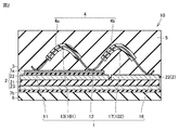
- FIG. 1 is a cross-sectional view schematically showing the configuration of the semiconductor device 10 according to the first embodiment.
- the height direction is used as a term indicating the direction.
- the height direction is a direction perpendicular to the circuit board 2.
- the semiconductor device 10 includes a bonding wire 1, a circuit board 2, a semiconductor element 3, a sealing material 4, a thermosetting resin 5, a base plate 6, and an upper bonding material 7a. And the lower bonding material 7b.
- the semiconductor device 10 is a power semiconductor device for electric power.
- a circuit board 2 is arranged on the base plate 6.
- the circuit board 2 is joined to the upper surface of the base plate 6 by the lower joining material 7.
- the material of the base plate 6 is, for example, copper (Cu) or a silicon carbide particle-reinforced aluminum composite material (AlSiC).
- the heat generated by the semiconductor element 3 is released to the outside by the base plate 6.
- the base plate 6 and the lower bonding material 7b may not be provided. When the base plate 6 and the lower bonding material 7b are not provided, the heat generated in the semiconductor device 10 is released to the outside by the lower conductor pattern 23 described later.
- the material of the upper bonding material 7a and the lower bonding material 7b is, for example, solder or a sinterable silver particle material.
- the circuit board 2 includes an insulating layer 21, an upper conductor pattern 22, and a lower conductor pattern 23.
- the insulating layer 21 is sandwiched between the upper conductor pattern 22 and the lower conductor pattern 23.
- the upper conductor pattern 22, the insulating layer 21, and the lower conductor pattern 23 are laminated in the order of the upper conductor pattern 22, the insulating layer 21, and the lower conductor pattern 23 in the height direction.
- the material of the insulating layer 21 is, for example, alumina (Al 2 O 3 ) or aluminum nitride (Al N). Further, when the base plate 6 and the lower bonding material 7b are not provided, the material of the insulating layer 21 may be a resin having an insulating property.
- the upper conductor pattern 22 is arranged on the upper surface of the insulating layer 21.
- the upper conductor pattern 22 is bonded to the semiconductor element 3 by the upper bonding material 7a.
- the lower conductor pattern 23 is arranged on the lower surface of the insulating layer 21.
- the lower conductor pattern 23 is joined to the upper surface of the base plate 6 by the lower bonding material 7b.
- the material of the upper conductor pattern 22 and the lower conductor pattern 23 is, for example, copper (Cu) or the like.
- Each of the upper conductor pattern 22 and the lower conductor pattern 23 may have a two-layer structure.
- Each of the upper conductor pattern 22 and the lower conductor pattern 23 is, for example, an aluminum (Al) layer formed on the surface of the insulating layer 21 and a copper (Cu) layer formed on the surface of the aluminum (Al) layer. And may be included.
- thermosetting resin 5 is arranged on the upper surface of the upper conductor pattern 22.
- the upper surface of the upper conductor pattern 22 may be provided with irregularities (not shown) by laser processing, a solvent, or the like. Further, the upper surface of the upper conductor pattern 22 may be coated with a coating (not shown) for improving the adhesion with the thermosetting resin 5. The unevenness or coating (not shown) prevents the thermosetting resin 5 from peeling off from the upper surface of the upper conductor pattern 22. Further, the lower surface of the lower conductor pattern 23 may also be provided with irregularities or coatings (not shown).
- the semiconductor element 3 is arranged on the circuit board 2.
- the semiconductor element 3 is bonded to the upper conductor pattern 22 by the upper bonding material 7a.
- the semiconductor element 3 may be, for example, a switching element such as an insulated gate type bipolar transistor (IGBT: Insulated Gate Bipolar Transistor) and a metal oxide semiconductor field effect transistor (MOSFET: Metal Oxide Semiconductor Field Effect Transistor), or a shot. It may be a rectifying element such as a key barrier diode.
- a surface electrode (not shown) is provided on the surface of the semiconductor element 3.
- the material of the surface electrode is, for example, aluminum (Al) or an aluminum alloy in which silicon (Si) is added to aluminum (Al).
- a coating layer (not shown) may be further provided on the surface of the surface electrode (not shown).
- the material of the coating layer (not shown) is, for example, nickel (Ni) or gold (Au).
- the material of the semiconductor element 3 is, for example, silicon (Si).
- the coefficient of linear expansion of the semiconductor element 3 formed of silicon (Si) is, for example, 3 ⁇ 10 -6 / K.
- the elastic modulus of the semiconductor element 3 formed of silicon (Si) is, for example, 70 GPa.
- the material of the semiconductor element 3 may be, for example, a wide bandgap semiconductor material having a bandgap larger than that of silicon (Si).
- the material of the semiconductor element 3 is preferably a wide bandgap semiconductor material. Wide bandgap semiconductor materials include, for example, silicon carbide (SiC), gallium nitride (GaN), diamond, and the like.
- the semiconductor element 3 formed of the wide bandgap semiconductor material has a higher allowable current density than the semiconductor element 3 formed of silicon (Si). Further, the power loss of the semiconductor element 3 formed of the wide bandgap semiconductor material is smaller than that of the semiconductor element 3 formed of silicon (Si). Therefore, by using a wide-gap semiconductor material as the material of the semiconductor element 3, the size of the semiconductor device 10 can be reduced.
- the upper limit of the operating temperature of the semiconductor element 3 formed of the wide bandgap semiconductor material is higher than that of the semiconductor element 3 formed of silicon (Si).
- the temperature of the semiconductor element 3 is high.
- the temperature of the semiconductor element 3 is, for example, 150 ° C. or higher.
- the temperature of the semiconductor element 3 is, for example, 200 ° C. or higher.
- the bonding wire 1 includes a first connecting portion 11, a second connecting portion 12, and a first loop portion 101.
- the first connection portion 11 is connected to the semiconductor element 3.
- the second connection portion 12 is connected to either the semiconductor element 3 or the circuit board 2.
- the first loop portion 101 is located between the first connection portion 11 and the second connection portion 12.
- the first loop portion 101 has a first bent portion 13.
- the second connection portion 12 is connected to the circuit board 2.
- the second connecting portion 12 may be connected to the semiconductor element 3.
- the bonding wire 1 is bonded to the semiconductor element 3 and the circuit board 2 by, for example, ultrasonic bonding.
- the bonding wire 1 electrically connects a surface electrode (not shown) of the semiconductor element 3 and the upper surface of the upper conductor pattern 22 of the circuit board 2.
- the bonding wire 1 is formed in a loop shape by the first loop portion 101.
- the first loop portion of the bonding wire is bent at the first bent portion 13.
- the first loop portion 101 projects upward with respect to the circuit board 2.
- the first loop portion 101 has a first portion 14 and a second portion 15.
- the first portion 14 connects the first connecting portion 11 and the first bent portion 13.
- the second portion 15 connects the second connecting portion 12 and the first bent portion 13.
- the first portion 14 extends in a direction intersecting the second portion 15.
- the first bent portion 13 is connected to the first portion 14 and the second portion 15.
- the first portion 14 and the second portion 15 face each other with the first bent portion 13 interposed therebetween.
- the first portion 14 and the second portion 15 may be exposed from the sealing material 4.
- the bonding wire 1 is sealed with a thermosetting resin 5.
- the bonding wire 1 is bound to the thermosetting resin 5.
- the first connecting portion 11 and the second connecting portion 12 are sealed with the thermosetting resin 5 while being exposed from the sealing material 4.
- the first bent portion 13 is sealed with a thermosetting resin 5 while being covered with a sealing material 4.
- the first bent portion 13 is not in direct contact with the thermosetting resin 5.
- the upper end of the bonding wire 1 is covered with a sealing material 4.
- the lower end of the bonding wire 1 is sealed with a thermosetting resin 5.
- the material of the bonding wire 1 is a conductive metal such as aluminum (Al) or copper (Cu).
- the coefficient of linear expansion of the bonding wire 1 is, for example, 2.3 ⁇ 10-5 / K.
- the elastic modulus of the bonding wire 1 is, for example, 70 GPa.
- the sealing material 4 covers the first bent portion 13 of the first loop portion 101.
- the sealing material 4 has a lower elastic modulus than the thermosetting resin 5.
- the sealing material 4 does not cover the first connecting portion 11 and the second connecting portion 12.
- the sealing material 4 is sealed with a thermosetting resin 5. Since the sealing material 4 has a lower elastic modulus than the thermosetting resin 5 and covers the first bent portion 13, it functions as a cushioning material for the first bent portion 13.
- the sealing material 4 may have a lower elastic modulus than the bonding wire 1.
- the shape of the sealing material 4 may be appropriately determined as long as the first bent portion 13 is covered.
- the sealing material 4 may have a shape along the first bent portion 13 as shown in FIG. 1, or may have a substantially spherical shape as shown in FIG. 7. ..
- the material of the sealing material 4 is different from the material of the thermosetting resin 5.
- the sealing material 4 is softer than the thermosetting resin 5. Inside the sealing material 4, the first bent portion 13 is deformable.
- the material of the sealing material 4 is, for example, polyimide.
- Polyimide generally has a lower elastic modulus than the epoxy resin which is the material of the thermosetting resin 5.
- Polyimide generally has higher strength and higher heat resistance than other polymer compounds.
- Polyimide has electrical insulating properties and is therefore used as an insulating material. From the above, the sealing material 4 has high strength, high heat resistance, and electrical insulation.
- the difference between the linear expansion coefficient of the sealing material 4 and the linear expansion coefficient of the bonding wire 1 may be smaller than the difference between the linear expansion coefficient of the thermosetting resin 5 and the linear expansion coefficient of the bonding wire 1.
- polyimide has a relatively low coefficient of linear expansion among organic substances.
- polyimide has a coefficient of linear expansion that is relatively close to that of metal among organic substances. Therefore, since the thermal strain of the sealing material 4 formed of polyimide and the thermal strain of the bonding wire 1 formed of metal are close to each other, thermal stress is unlikely to occur in the bonding wire 1.
- the sealing material 4 may be a liquid having a constant viscosity in an uncured state and a normal temperature state.
- the material of the sealing material 4 may be appropriately determined according to the bonding wire 1.
- the sealing material 4 includes the first sealing portion 4a and the second sealing portion 4b as shown in FIG. 2, the materials of the first sealing portion 4a and the second sealing portion 4b are different. You may be.
- a material in which a plurality of materials are appropriately combined may be used as the material of the sealing material 4.
- thermosetting resin 5 seals the circuit board 2, the semiconductor element 3, the bonding wire 1, and the sealing material 4. Specifically, the thermosetting resin 5 seals the first connection portion 11 and the second connection portion 12 of the bonding wire 1.
- the thermosetting resin 5 reinforces the first connection portion 11 and the second connection portion 12 by sealing the first connection portion 11 and the second connection portion 12.
- the thermosetting resin 5 sandwiches the sealing material 4 to seal the first bent portion 13.
- the thermosetting resin 5 has a higher elastic modulus than the sealing material 4. The deformation of the bonding wire 1 is suppressed inside the thermosetting resin 5.
- the thermosetting resin 5 has an insulating property.
- the material of the thermosetting resin 5 is, for example, an epoxy resin.
- the elastic modulus of the epoxy resin is, for example, 5 GPa.
- the thermosetting resin 5 has a coefficient of linear expansion different from that of the bonding wire 1.
- the coefficient of linear expansion of the epoxy resin is, for example, 2.0 ⁇ 10-5 / K.
- the temperature of the semiconductor device 10 becomes high during operation, for example, 200 ° C.
- the thermosetting resin 5 is formed of a resin having a low glass transition temperature, the elasticity of the thermosetting resin 5 may decrease due to the softening or deterioration of the thermosetting resin 5 due to the high temperature.
- the reinforcement of the first connection portion 11 and the second connection portion 12 by the thermosetting resin 5 is impaired, so that the reliability of the first connection portion 11 and the second connection portion 12 may decrease. Therefore, the material of the thermosetting resin 5 is preferably a material that is suppressed from deteriorating at a high temperature. In order to prevent the thermosetting resin 5 from deteriorating due to high temperature, it is desirable that the thermosetting resin 5 contains a metal or filler (not shown).
- the bonding wire 1 further includes a third connecting portion 16 and a second loop portion 102.
- the third connection portion 16 is connected to either the semiconductor element 3 or the circuit board 2.
- the second loop portion 102 is located between the second connecting portion 12 and the third connecting portion 16.
- the second loop portion 102 has a second bent portion 17.
- the second connecting portion 12 is connected to the semiconductor element 3, and the third connecting portion 16 is connected to the circuit board 2.
- the sealing material 4 covers each of the first bent portion 13 and the second bent portion 17.
- the sealing material 4 includes a first sealing portion 4a and a second sealing portion 4b.
- the first sealing portion 4a covers the first bent portion 13.
- the second sealing portion 4b covers the second bent portion 17.
- the first sealing portion 4a is separated from the second sealing portion 4b.
- the first sealing portion 4a and the second sealing portion 4b are separate bodies.
- the third connecting portion 16 is exposed from the sealing material 4.
- the heat generated in the semiconductor element 3 is dissipated by the following path shown in FIG. 1, so that the semiconductor device 10 is cooled. That is, the heat generated in the semiconductor element 3 moves in the order of the upper bonding material 7a, the upper conductor pattern 22, the insulating layer 21, the lower conductor pattern 23, the lower bonding material 7b, and the base plate 6, and the semiconductor from the base plate 6 The heat is dissipated to the outside of the device 10. As a result, the temperature of the semiconductor device 10 is lowered. Specifically, the temperature of the semiconductor element 3 drops sharply.
- Deformation occurs in the semiconductor device 10 due to changes in the temperature of the semiconductor device 10. Specifically, when the temperature of the semiconductor device 10 rises, the bonding wire 1, the sealing material 4, and the thermosetting resin 5 thermally expand. Further, when the temperature of the semiconductor device 10 decreases, the bonding wire 1, the sealing material 4, and the thermosetting resin 5 are thermally shrunk. As the temperature change (temperature swing) of the semiconductor device 10 increases, the amount of deformation of the semiconductor device 10 increases.
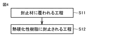
- FIG. 3 is a cross-sectional view showing the configuration of the semiconductor device 10 according to the comparative example.
- the semiconductor device 10 according to the comparative example does not include the sealing material 4. Therefore, the first bent portion 13 of the first loop portion 101 of the bonding wire 1 of the semiconductor device 10 according to the comparative example shown in FIG. 3 is sealed with the thermosetting resin 5. Therefore, in the comparative example, the deformation of the first bent portion 13 is hindered by the thermosetting resin 5.
- the thermal stress of the first portion 14 in the direction along the first portion 14 and the thermal stress of the second portion 15 in the direction along the second portion 15 Is generated in the first bent portion 13. That is, since the first bent portion 13 is bent, thermal stress in two different directions is generated in the first bent portion 13 as the temperature of the semiconductor device 10 changes. Therefore, thermal stress is concentrated on the first bent portion 13.
- the thermal stress generated in the first bent portion 13 is large, cracks may occur in the first bent portion 13.
- the crack can gradually develop by repeating the temperature change of the semiconductor device 10. If the crack grows, the bonding wire 1 can be shredded.
- the first bent portion 13 is a sealing material 4 having a lower elastic modulus than the thermosetting resin 5. It is covered. Therefore, the deformation of the first bent portion 13 is not hindered as compared with the comparative example. Therefore, the concentration of thermal stress on the first bent portion 13 is alleviated. Therefore, cracks are prevented from occurring in the first bent portion 13 and extending.
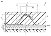
- the method for manufacturing the semiconductor device 10 includes a step S11 of being covered with the sealing material 4 and a step S12 of being sealed with the thermosetting resin 5.
- the step S11 covered with the sealing material 4 the first bent portion 13 of the first loop portion 101 of the bonding wire 1 is covered with the sealing material 4.
- the step S12 of sealing with the thermosetting resin 5 the circuit board 2, the semiconductor element 3, the bonding wire 1, and the sealing material 4 are sealed with the thermosetting resin 5.
- the bonding wire 1, the circuit board 2, the semiconductor element 3, the base plate 6, the upper bonding material 7a and the lower bonding material 7b shown in FIG. 1 are bonded by the following process.
- the upper conductor pattern 22 of the circuit board 2 is joined to the semiconductor element 3 by the upper bonding material 7a.
- the lower conductor pattern 23 of the circuit board 2 is joined to the base plate 6 by the lower bonding material 7b.
- the first connection portion 11 of the bonding wire 1 is bonded to the semiconductor element 3 by ultrasonic bonding.
- the second connecting portion 12 is bonded to the semiconductor element 3 or the circuit board 2 by ultrasonic bonding. In the present embodiment, the second connection portion 12 is joined to the circuit board 2.
- the bonding wire 1 may be bonded to the circuit board 2 and the semiconductor element 3 after the semiconductor element 3 and the base plate 6 are bonded to the circuit board 2.
- the semiconductor element 3 and the base plate 6 may be bonded to the circuit board 2 after the bonding wire 1 is bonded to the circuit board 2 and the semiconductor element 3.
- the sealing material 4 is applied by being dropped onto the bonding wire 1 by, for example, a dispenser or the like. As a result, as shown in FIG. 1, the first bent portion 13 of the first loop portion 101 of the bonding wire 1 is covered with the sealing material 4.
- the method of applying the sealing material 4 to the first bent portion 13 is not limited to a dispenser or the like.
- the sealing material 4 may be applied by immersing the first bent portion 13 in the sealing material 4.
- a container filled with the liquid sealing material 4 may be prepared and installed on a table or the like.
- the circuit board 2 to which the semiconductor element 3, the base plate 6, and the bonding wire 1 are bonded is held so that the bonding wire 1 is located below the circuit board 2. Only the first bent portion 13 of the first loop portion 101 of the bonding wire 1 of the circuit board 2 to which the semiconductor element 3, the base plate 6 and the bonding wire 1 are bonded is immersed in the container filled with the sealing material 4.
- the sealing material 4 is applied. After that, the circuit board 2 to which the semiconductor element 3, the base plate 6, and the bonding wire 1 are bonded is lifted. As a result, the bonding wire 1 in which the sealing material 4 is applied to the first bent portion 13 of the first loop portion 101 is obtained.
- the sealing material 4 is applied to the bonding wire 1 and then sealed in the thermosetting resin 5
- the circuit board 2, the semiconductor element 3, and the bonding wire 1 are as shown in FIG. ,
- the sealing material 4 is sealed in the thermosetting resin 5.
- the sealing material 4 covering the first bent portion 13 of the first loop portion 101 of the bonding wire 1 is made of a thermosetting resin 5. Also has a low elastic modulus. Therefore, the first bent portion 13 is more easily deformed inside the sealing material 4 than when the first bent portion 13 is sealed with the thermosetting resin 5. Therefore, the thermal stress generated in the first bent portion 13 can be reduced as compared with the case where the first bent portion 13 is sealed with the thermosetting resin 5. Therefore, the growth of cracks at the first bent portion 13 can be suppressed.
- the first connection portion 11 and the second connection portion 12 are heated. Stress can occur.
- the semiconductor device 10 of the present embodiment as shown in FIG. 1, the first connection portion 11 and the second connection portion 12 are sealed with a thermosetting resin 5. Thereby, the first connection portion 11 and the second connection portion 12 can be reinforced. Further, since the deformation generated in the first connection portion 11 and the second connection portion 12 is distributed in the thermosetting resin 5, it is possible to prevent the thermal stress from concentrating on the first connection portion 11 and the second connection portion 12. ..
- Wire lift-off means that the bonding wire 1 is separated from the semiconductor element 3 or the circuit board 2 due to the growth of cracks generated by the thermal stress repeatedly applied to the first connection portion 11 or the second connection portion 12 due to the temperature change. It is a phenomenon that occurs.
- the sealing material 4 When the material of the sealing material 4 is polyimide or the like having an insulating property, the sealing material 4 can also insulate the semiconductor device 10 and the outside of the semiconductor device 10 in the same manner as the thermosetting resin 5. Therefore, even when the sealing material 4 covers the bonding wire 1, it is possible to prevent the insulating property from being lowered.
- the respective materials of the sealing material 4 and the thermosetting resin 5 can be appropriately selected.
- the materials of the sealing material 4 and the thermosetting resin 5 can be optimally selected according to the required properties.
- the materials of the sealing material 4 and the thermosetting resin 5 have, for example, the presence or absence of insulation, the elastic modulus, the linear expansion coefficient, the heat dissipation, the shape of the first loop portion 101 of the adhesive strength, the curvature of the first bent portion 13, and the like. You can choose according to your needs.
- the difference between the linear expansion coefficient of the sealing material 4 and the linear expansion coefficient of the bonding wire 1 is smaller than the difference between the linear expansion coefficient of the thermosetting resin 5 and the linear expansion coefficient of the bonding wire 1.
- the materials of the material 4 and the thermosetting resin 5 can be selected. Thereby, the thermal stress generated in the bonding wire 1 can be reduced.
- the first bent portion 13 and the second bent portion 17 are respectively the first sealing portion 4a and the second sealing portion. Since it is covered by each of 4b, the material of the sealing material 4 can be selected according to the first bent portion 13 and the second bent portion 17. Therefore, the sealing material 4 can be optimally selected.
- the first bent portion 13 is covered with a sealing material 4 having an elastic modulus lower than that of the thermosetting resin 5, and then the thermosetting resin 5 is covered. Is sealed in. Therefore, the thermal stress generated in the first bent portion 13 can be reduced. As a result, the growth of cracks at the first bent portion 13 can be suppressed.
- Embodiment 2 Unless otherwise specified, the second embodiment has the same configuration, manufacturing method, and action and effect as those of the first embodiment. Therefore, the same components as those in the first embodiment are designated by the same reference numerals, and the description will not be repeated.
- FIG. 5 is a cross-sectional view schematically showing the configuration of the semiconductor device 10 according to the second embodiment.
- the sealing material 4 is located above the height position H, which is half the height from the first connecting portion 11 of the bonding wire 1 to the upper end of the first loop portion 101.
- the sealing material 4 is not located below the height position H, which is half the height from the first connecting portion 11 to the upper end of the first loop portion 101.
- a part of the sealing material 4 is located above the height of the upper end of the first loop portion 101.
- the first bent portion 13 is located above the height position H, which is half the height from the first connecting portion 11 to the upper end of the first loop portion 101.
- the first connection portion 11 and the second connection portion 12 are located below the height position H, which is half the height from the first connection portion 11 to the upper end of the first loop portion 101.
- At least a part of the upper half of the first loop portion 101 is covered with the sealing material 4.
- the lower half of the first loop portion 101 is not covered with the sealing material 4.
- the first bent portion 13 has a radius of curvature larger than 2 mm.
- the first bent portion 13 may have a first major bent portion 131 and a second major bent portion 132.
- the first major bending portion 131 and the second major bending portion 132 are connected by a third portion 18 of the first loop portion 101.
- the first portion 14, the second portion 15, and the third portion 18 have, for example, a radius of curvature of 2 mm or less.
- the first bent portion 13 has a radius of curvature larger than that of the first portion 14, the second portion 15, and the third portion 18.
- the sealing material 4 has a third sealing portion 4c and a fourth sealing portion 4d.
- the sealing material 4 covers only the portion of the first loop portion 101 having a large radius of curvature. Specifically, the third sealing portion 4c covers the first large bending portion 131.
- the fourth sealing portion 4d covers the second large bending portion 132.
- the sealing material 4 is above the half height position H from the first connecting portion 11 to the upper end of the first loop portion 101. Since it is located at and not below the height position H, the amount of the sealing material 4 contained in the semiconductor device 10 can be reduced. Therefore, the manufacturing cost of the semiconductor device 10 can be reduced.
- the sealing material 4 since the first bent portion 13 has a radius of curvature larger than 2 mm, the sealing material 4 has a radius of curvature smaller than 2 mm. It does not cover the portion of the first loop portion 101. Therefore, the amount of the sealing material 4 contained in the semiconductor device 10 can be further reduced. Therefore, the manufacturing cost of the semiconductor device 10 can be reduced. In addition, in order to obtain the advantageous effect in the present embodiment, it is necessary to appropriately control the amount of the sealing material 4 applied to the first bent portion 13.
- Embodiment 3 Unless otherwise specified, the third embodiment has the same configuration, manufacturing method, and action and effect as those of the first embodiment. Therefore, the same components as those in the first embodiment are designated by the same reference numerals, and the description will not be repeated.
- FIG. 7 is a cross-sectional view schematically showing the configuration of the semiconductor device 10 according to the third embodiment.
- the sealing material 4 fills a region between the first bent portion 13 and at least one of the semiconductor element 3 and the circuit board 2, and is in contact with at least one of the semiconductor element 3 and the circuit board 2.
- the sealing material 4 fills the region between the first bent portion 13 and the semiconductor element 3 and the circuit board 2, and is in contact with both the semiconductor element 3 and the circuit board 2.
- the sealing material 4 integrally covers the first bent portion 13 and at least a part of at least one of the semiconductor element 3 and the circuit board 2.
- the sealing material 4 is adhered to at least one of the semiconductor element 3 and the circuit board 2.
- the material of the sealing material 4 needs to have an insulating property.
- the sealing material 4 may cover the first loop portion 101 except for the vicinity of the first connecting portion 11 and the second connecting portion 12.
- the first bent portion 13 is covered with the sealing material 4. Further, the region between the first bent portion 13 and at least one of the semiconductor element 3 and the circuit board 2 is filled with the sealing material 4. Further, the sealing material 4 is arranged so as to be in contact with at least one of the semiconductor element 3 and the circuit board 2. The sealing material 4 is dropped so as to fill a region between the first bent portion 13 and at least one of the semiconductor element 3 and the circuit board 2.
- the sealing material 4 fills the region between the first bent portion 13 and at least one of the semiconductor element 3 and the circuit board 2. It is arranged so as to be in contact with at least one of the semiconductor element 3 and the circuit board 2. Therefore, the amount of the sealing material 4 is larger than that in the case where the sealing material 4 is applied only to the first bent portion 13. The permissible variation in the amount of the sealing material 4 applied is large. Therefore, the amount of the sealing material 4 applied does not need to be strictly controlled. Therefore, since the manufacturing method of the semiconductor device 10 is simplified, the manufacturing cost of the semiconductor device 10 can be reduced.
- Embodiment 4 Unless otherwise specified, the fourth embodiment has the same configuration, manufacturing method, and action and effect as those of the first embodiment. Therefore, the same components as those in the first embodiment are designated by the same reference numerals, and the description will not be repeated.
- the sealing material 4 integrally covers the first bent portion 13 of the first loop portion 101 and the second bent portion 17 of the second loop portion 102.
- the material of the sealing material 4 has an insulating property.
- the bonding wire 1 includes a plurality of loop portions.
- the bonding wire 1 includes a plurality of wire portions. Specifically, the bonding wire 1 includes a first wire portion 1a and a second wire portion 1b.
- the first bent portion 13 has a first wire portion bent portion 13a and a second wire portion bent portion 13b.
- the first wire portion bent portion 13a is included in the first wire portion 1a.
- the second wire portion bent portion 13b is included in the second wire portion 1b.
- the sealing material 4 integrally covers the first wire portion bent portion 13a and the second wire portion bent portion 13b.
- the first wire portion 1a is electrically connected to the second wire portion 1b.
- the first wire portion 1a has a first wire portion loop portion 101a.
- the second wire portion 1b has a second wire portion loop portion 101b.
- the first connection portion 11 has a first wire portion first connection portion 11a and a second wire portion first connection portion 11b.
- the second connection portion 12 has a first wire portion second connection portion 12a and a second wire portion second connection portion 12b.
- the first wire portion first connection portion 11a and the first wire portion second connection portion 12a are included in the first wire portion 1a.
- the second wire portion first connection portion 11b and the second wire portion second connection portion 12b are included in the second wire portion 1b.
- the first wire portion bent portion 13a is included in the first wire portion loop portion 101a located between the first wire portion first connection portion 11a and the first wire portion second connection portion 12a.
- the second wire portion bent portion 13b is included in the second wire portion loop portion 101b located between the second wire portion first connection portion 11b and the second wire portion second connection portion 12b.
- the sealing material 4 forms the first bent portion 13 of the first loop portion 101 and the second bent portion 17 of the second loop portion 102. Since it is integrally covered, the first bent portion 13 and the second bent portion 17 can be simultaneously covered by the sealing material 4 in the step S11 covered by the sealing material 4. Therefore, the manufacturing process can be simplified as compared with the case where each of the first bent portion 13 and the second bent portion 17 is individually covered. Therefore, even when the bonding wire 1 includes a plurality of loop portions, the manufacturing cost of the semiconductor device 10 can be reduced.
- the bonding wire 1 integrally covers the first wire portion bent portion 13a and the second wire portion bent portion 13b. Therefore, in the step S11 covered by the sealing material 4, the first wire portion bent portion 13a and the second wire portion bent portion 13b can be simultaneously covered by the sealing material 4. Therefore, the manufacturing process can be simplified as compared with the case where each of the first wire portion bent portion 13a and the second wire portion bent portion 13b is individually covered. Therefore, even when the bonding wire 1 has a plurality of wire portions, the manufacturing cost of the semiconductor device 10 can be reduced.
- Embodiment 5 the semiconductor devices according to the above-described first to fourth embodiments are applied to a power conversion device.
- the present invention is not limited to a specific power conversion device, the case where the present invention is applied to a three-phase inverter will be described below as a fifth embodiment.
- FIG. 10 is a block diagram showing a configuration of a power conversion system to which the power conversion device according to the present embodiment is applied.
- the power conversion system shown in FIG. 10 includes a power supply 100, a power conversion device 200, and a load 300.
- the power supply 100 is a DC power supply, and supplies DC power to the power converter 200.
- the power supply 100 can be configured with various things, for example, it can be configured with a DC system, a solar cell, a storage battery, or it can be configured with a rectifier circuit or an AC / DC converter connected to an AC system. May be good.
- the power supply 100 may be configured by a DC / DC converter that converts the DC power output from the DC system into a predetermined power.
- the power conversion device 200 is a three-phase inverter connected between the power supply 100 and the load 300, converts the DC power supplied from the power supply 100 into AC power, and supplies AC power to the load 300. As shown in FIG. 10, the power conversion device 200 has a main conversion circuit 201 that converts DC power into AC power and outputs it, and a control circuit 203 that outputs a control signal for controlling the main conversion circuit 201 to the main conversion circuit 201. And have.
- the load 300 is a three-phase electric motor driven by AC power supplied from the power converter 200.
- the load 300 is not limited to a specific application, and is an electric motor mounted on various electric devices.
- the load 300 is used as an electric motor for a hybrid vehicle, an electric vehicle, a railroad vehicle, an elevator, or an air conditioner.
- the main conversion circuit 201 includes a switching element and a freewheeling diode (not shown), and when the switching element switches, the DC power supplied from the power supply 100 is converted into AC power and supplied to the load 300.
- the main conversion circuit 201 is a two-level three-phase full bridge circuit, and has six switching elements and each switching element. It can consist of six anti-parallel freewheeling diodes.
- Each switching element and each freewheeling diode of the main conversion circuit 201 are configured by a semiconductor module 202 corresponding to any one of the above-described first to fourth embodiments.
- the six switching elements are connected in series for each of the two switching elements to form an upper and lower arm, and each upper and lower arm constitutes each phase (U phase, V phase, W phase) of the full bridge circuit. Then, the output terminals of the upper and lower arms, that is, the three output terminals of the main conversion circuit 201 are connected to the load 300.
- the main conversion circuit 201 includes a drive circuit (not shown) for driving each switching element
- the drive circuit may be built in the semiconductor module 202, or a drive circuit may be provided separately from the semiconductor module 202. It may be provided.
- the drive circuit generates a drive signal for driving the switching element of the main conversion circuit 201 and supplies the drive signal to the control electrode of the switching element of the main conversion circuit 201.
- a drive signal for turning on the switching element and a drive signal for turning off the switching element are output to the control electrodes of each switching element.
- the drive signal When the switching element is kept on, the drive signal is a voltage signal (on signal) equal to or higher than the threshold voltage of the switching element, and when the switching element is kept off, the drive signal is a voltage equal to or lower than the threshold voltage of the switching element. It becomes a signal (off signal).
- the control circuit 203 controls the switching element of the main conversion circuit 201 so that the desired power is supplied to the load 300. Specifically, the time (on time) at which each switching element of the main conversion circuit 201 should be in the on state is calculated based on the power to be supplied to the load 300.
- the main conversion circuit 201 can be controlled by PWM control that modulates the on-time of the switching element according to the voltage to be output. Then, a control command (control signal) is output to the drive circuit included in the main conversion circuit 201 so that an on signal is output to the switching element that should be turned on at each time point and an off signal is output to the switching element that should be turned off. Is output.
- the drive circuit outputs an on signal or an off signal as a drive signal to the control electrode of each switching element according to this control signal.
- the semiconductor module according to the first to fourth embodiments is applied as the switching element of the main conversion circuit 201 and the freewheeling diode, cracks occur at the first bent portion of the bonding wire and cracks occur. The progress can be suppressed.
- the present invention is not limited to this, and can be applied to various power conversion devices.
- a two-level power conversion device is used, but a three-level or multi-level power conversion device may be used. You may apply it.
- the present invention can be applied to a DC / DC converter or an AC / DC converter.
- the power conversion device to which the present invention is applied is not limited to the case where the above-mentioned load is an electric motor, and is, for example, a power supply device for a discharge machine, a laser machine, an induction heating cooker, or a non-contact power supply system. It can also be used as a power conditioner for a photovoltaic power generation system, a power storage system, or the like.
- thermosetting resin 10 semiconductor device, 11 1st connection part, 12 2nd connection part , 13 1st bent part, 13a 1st wire part bent part, 13b 2nd wire part bent part, 16 3rd connection part, 17 2nd bent part, 100 power supply, 101 1st loop part, 102 2nd loop part, 200 power converter, 201 main conversion circuit, 202 semiconductor module, 203 circuit board, 300 load, H height position.
Landscapes
- Structures Or Materials For Encapsulating Or Coating Semiconductor Devices Or Solid State Devices (AREA)
Priority Applications (2)
| Application Number | Priority Date | Filing Date | Title |
|---|---|---|---|
| JP2021551071A JP7229382B2 (ja) | 2019-10-11 | 2019-10-11 | 半導体装置、電力変換装置および半導体装置の製造方法 |
| PCT/JP2019/040224 WO2021070358A1 (ja) | 2019-10-11 | 2019-10-11 | 半導体装置、電力変換装置および半導体装置の製造方法 |
Applications Claiming Priority (1)
| Application Number | Priority Date | Filing Date | Title |
|---|---|---|---|
| PCT/JP2019/040224 WO2021070358A1 (ja) | 2019-10-11 | 2019-10-11 | 半導体装置、電力変換装置および半導体装置の製造方法 |
Publications (1)
| Publication Number | Publication Date |
|---|---|
| WO2021070358A1 true WO2021070358A1 (ja) | 2021-04-15 |
Family
ID=75438129
Family Applications (1)
| Application Number | Title | Priority Date | Filing Date |
|---|---|---|---|
| PCT/JP2019/040224 Ceased WO2021070358A1 (ja) | 2019-10-11 | 2019-10-11 | 半導体装置、電力変換装置および半導体装置の製造方法 |
Country Status (2)
| Country | Link |
|---|---|
| JP (1) | JP7229382B2 (https=) |
| WO (1) | WO2021070358A1 (https=) |
Citations (4)
| Publication number | Priority date | Publication date | Assignee | Title |
|---|---|---|---|---|
| JPH06333970A (ja) * | 1993-05-21 | 1994-12-02 | Seiko Epson Corp | 半導体装置およびその製造方法 |
| JP2013058606A (ja) * | 2011-09-08 | 2013-03-28 | Renesas Electronics Corp | 半導体装置の製造方法 |
| JP2017224778A (ja) * | 2016-06-17 | 2017-12-21 | 三菱電機株式会社 | 半導体装置 |
| WO2018211751A1 (ja) * | 2017-05-18 | 2018-11-22 | 三菱電機株式会社 | 半導体モジュールおよび電力変換装置 |
Family Cites Families (1)
| Publication number | Priority date | Publication date | Assignee | Title |
|---|---|---|---|---|
| JP2000100997A (ja) * | 1998-09-17 | 2000-04-07 | Mitsubishi Electric Corp | 樹脂封止型半導体装置およびその樹脂封止方法 |
-
2019
- 2019-10-11 WO PCT/JP2019/040224 patent/WO2021070358A1/ja not_active Ceased
- 2019-10-11 JP JP2021551071A patent/JP7229382B2/ja active Active
Patent Citations (4)
| Publication number | Priority date | Publication date | Assignee | Title |
|---|---|---|---|---|
| JPH06333970A (ja) * | 1993-05-21 | 1994-12-02 | Seiko Epson Corp | 半導体装置およびその製造方法 |
| JP2013058606A (ja) * | 2011-09-08 | 2013-03-28 | Renesas Electronics Corp | 半導体装置の製造方法 |
| JP2017224778A (ja) * | 2016-06-17 | 2017-12-21 | 三菱電機株式会社 | 半導体装置 |
| WO2018211751A1 (ja) * | 2017-05-18 | 2018-11-22 | 三菱電機株式会社 | 半導体モジュールおよび電力変換装置 |
Also Published As
| Publication number | Publication date |
|---|---|
| JP7229382B2 (ja) | 2023-02-27 |
| JPWO2021070358A1 (https=) | 2021-04-15 |
Similar Documents
| Publication | Publication Date | Title |
|---|---|---|
| JP6927437B1 (ja) | パワーモジュールおよび電力変換装置 | |
| JP6826665B2 (ja) | 半導体装置、半導体装置の製造方法及び電力変換装置 | |
| JPWO2019049400A1 (ja) | パワーモジュール及びその製造方法並びに電力変換装置 | |
| JP2018190930A (ja) | パワー半導体モジュール及びその製造方法並びに電力変換装置 | |
| JP7561677B2 (ja) | 電力半導体装置、電力半導体装置の製造方法及び電力変換装置 | |
| CN113646876A (zh) | 功率半导体模块以及电力变换装置 | |
| WO2020235056A1 (ja) | 半導体装置、電力変換装置および半導体装置の製造方法 | |
| US11450594B2 (en) | Semiconductor device and power converter | |
| WO2021157024A1 (ja) | 半導体モジュール及び電力変換装置 | |
| US11855033B2 (en) | Power semiconductor module and power converter | |
| JP7132340B2 (ja) | 半導体装置および電力変換装置 | |
| JP7287164B2 (ja) | 電力用半導体装置及び電力変換装置 | |
| JP7229382B2 (ja) | 半導体装置、電力変換装置および半導体装置の製造方法 | |
| JP6851559B1 (ja) | 半導体装置および電力変換装置 | |
| JP7334369B1 (ja) | パワーモジュール及び電力変換装置 | |
| JP2022029886A (ja) | 半導体装置、半導体装置の製造方法及び電力変換装置 | |
| JP7088421B1 (ja) | 半導体装置および電力変換装置 | |
| WO2025009015A1 (ja) | パワーモジュール及びその製造方法並びに電力変換装置 | |
| WO2024090278A1 (ja) | 半導体装置、電力変換装置および半導体装置の製造方法 | |
| WO2025099830A1 (ja) | パワー半導体装置、パワーモジュール及び電力変換装置 | |
| JP2022064644A (ja) | 半導体装置および電力変換装置 | |
| WO2022239154A1 (ja) | パワーモジュールおよび電力変換装置 | |
| WO2022064599A1 (ja) | 半導体装置および電力変換装置 | |
| WO2021100199A1 (ja) | 半導体装置およびその製造方法ならびに電力変換装置 | |
| JPWO2021033270A1 (ja) | 半導体装置、電力変換装置及び移動体 |
Legal Events
| Date | Code | Title | Description |
|---|---|---|---|
| 121 | Ep: the epo has been informed by wipo that ep was designated in this application |
Ref document number: 19948858 Country of ref document: EP Kind code of ref document: A1 |
|
| ENP | Entry into the national phase |
Ref document number: 2021551071 Country of ref document: JP Kind code of ref document: A |
|
| NENP | Non-entry into the national phase |
Ref country code: DE |
|
| 122 | Ep: pct application non-entry in european phase |
Ref document number: 19948858 Country of ref document: EP Kind code of ref document: A1 |