WO2021070358A1 - 半導体装置、電力変換装置および半導体装置の製造方法 - Google Patents
半導体装置、電力変換装置および半導体装置の製造方法 Download PDFInfo
- Publication number
- WO2021070358A1 WO2021070358A1 PCT/JP2019/040224 JP2019040224W WO2021070358A1 WO 2021070358 A1 WO2021070358 A1 WO 2021070358A1 JP 2019040224 W JP2019040224 W JP 2019040224W WO 2021070358 A1 WO2021070358 A1 WO 2021070358A1
- Authority
- WO
- WIPO (PCT)
- Prior art keywords
- sealing material
- semiconductor device
- wire
- bent portion
- circuit board
- Prior art date
Links
Images


Classifications
-
- H—ELECTRICITY
- H01—ELECTRIC ELEMENTS
- H01L—SEMICONDUCTOR DEVICES NOT COVERED BY CLASS H10
- H01L23/00—Details of semiconductor or other solid state devices
- H01L23/28—Encapsulations, e.g. encapsulating layers, coatings, e.g. for protection
- H01L23/29—Encapsulations, e.g. encapsulating layers, coatings, e.g. for protection characterised by the material, e.g. carbon
-
- H—ELECTRICITY
- H01—ELECTRIC ELEMENTS
- H01L—SEMICONDUCTOR DEVICES NOT COVERED BY CLASS H10
- H01L23/00—Details of semiconductor or other solid state devices
- H01L23/28—Encapsulations, e.g. encapsulating layers, coatings, e.g. for protection
- H01L23/31—Encapsulations, e.g. encapsulating layers, coatings, e.g. for protection characterised by the arrangement or shape
-
- H—ELECTRICITY
- H01—ELECTRIC ELEMENTS
- H01L—SEMICONDUCTOR DEVICES NOT COVERED BY CLASS H10
- H01L23/00—Details of semiconductor or other solid state devices
- H01L23/48—Arrangements for conducting electric current to or from the solid state body in operation, e.g. leads, terminal arrangements ; Selection of materials therefor
-
- H—ELECTRICITY
- H01—ELECTRIC ELEMENTS
- H01L—SEMICONDUCTOR DEVICES NOT COVERED BY CLASS H10
- H01L25/00—Assemblies consisting of a plurality of individual semiconductor or other solid state devices ; Multistep manufacturing processes thereof
- H01L25/03—Assemblies consisting of a plurality of individual semiconductor or other solid state devices ; Multistep manufacturing processes thereof all the devices being of a type provided for in the same subgroup of groups H01L27/00 - H01L33/00, or in a single subclass of H10K, H10N, e.g. assemblies of rectifier diodes
- H01L25/04—Assemblies consisting of a plurality of individual semiconductor or other solid state devices ; Multistep manufacturing processes thereof all the devices being of a type provided for in the same subgroup of groups H01L27/00 - H01L33/00, or in a single subclass of H10K, H10N, e.g. assemblies of rectifier diodes the devices not having separate containers
- H01L25/07—Assemblies consisting of a plurality of individual semiconductor or other solid state devices ; Multistep manufacturing processes thereof all the devices being of a type provided for in the same subgroup of groups H01L27/00 - H01L33/00, or in a single subclass of H10K, H10N, e.g. assemblies of rectifier diodes the devices not having separate containers the devices being of a type provided for in group H01L29/00
-
- H—ELECTRICITY
- H01—ELECTRIC ELEMENTS
- H01L—SEMICONDUCTOR DEVICES NOT COVERED BY CLASS H10
- H01L25/00—Assemblies consisting of a plurality of individual semiconductor or other solid state devices ; Multistep manufacturing processes thereof
- H01L25/18—Assemblies consisting of a plurality of individual semiconductor or other solid state devices ; Multistep manufacturing processes thereof the devices being of types provided for in two or more different subgroups of the same main group of groups H01L27/00 - H01L33/00, or in a single subclass of H10K, H10N
-
- H—ELECTRICITY
- H01—ELECTRIC ELEMENTS
- H01L—SEMICONDUCTOR DEVICES NOT COVERED BY CLASS H10
- H01L2224/00—Indexing scheme for arrangements for connecting or disconnecting semiconductor or solid-state bodies and methods related thereto as covered by H01L24/00
- H01L2224/01—Means for bonding being attached to, or being formed on, the surface to be connected, e.g. chip-to-package, die-attach, "first-level" interconnects; Manufacturing methods related thereto
- H01L2224/26—Layer connectors, e.g. plate connectors, solder or adhesive layers; Manufacturing methods related thereto
- H01L2224/31—Structure, shape, material or disposition of the layer connectors after the connecting process
- H01L2224/32—Structure, shape, material or disposition of the layer connectors after the connecting process of an individual layer connector
- H01L2224/321—Disposition
- H01L2224/32151—Disposition the layer connector connecting between a semiconductor or solid-state body and an item not being a semiconductor or solid-state body, e.g. chip-to-substrate, chip-to-passive
- H01L2224/32221—Disposition the layer connector connecting between a semiconductor or solid-state body and an item not being a semiconductor or solid-state body, e.g. chip-to-substrate, chip-to-passive the body and the item being stacked
- H01L2224/32225—Disposition the layer connector connecting between a semiconductor or solid-state body and an item not being a semiconductor or solid-state body, e.g. chip-to-substrate, chip-to-passive the body and the item being stacked the item being non-metallic, e.g. insulating substrate with or without metallisation
-
- H—ELECTRICITY
- H01—ELECTRIC ELEMENTS
- H01L—SEMICONDUCTOR DEVICES NOT COVERED BY CLASS H10
- H01L2224/00—Indexing scheme for arrangements for connecting or disconnecting semiconductor or solid-state bodies and methods related thereto as covered by H01L24/00
- H01L2224/01—Means for bonding being attached to, or being formed on, the surface to be connected, e.g. chip-to-package, die-attach, "first-level" interconnects; Manufacturing methods related thereto
- H01L2224/42—Wire connectors; Manufacturing methods related thereto
- H01L2224/47—Structure, shape, material or disposition of the wire connectors after the connecting process
- H01L2224/48—Structure, shape, material or disposition of the wire connectors after the connecting process of an individual wire connector
- H01L2224/481—Disposition
- H01L2224/4813—Connecting within a semiconductor or solid-state body, i.e. fly wire, bridge wire
-
- H—ELECTRICITY
- H01—ELECTRIC ELEMENTS
- H01L—SEMICONDUCTOR DEVICES NOT COVERED BY CLASS H10
- H01L2224/00—Indexing scheme for arrangements for connecting or disconnecting semiconductor or solid-state bodies and methods related thereto as covered by H01L24/00
- H01L2224/01—Means for bonding being attached to, or being formed on, the surface to be connected, e.g. chip-to-package, die-attach, "first-level" interconnects; Manufacturing methods related thereto
- H01L2224/42—Wire connectors; Manufacturing methods related thereto
- H01L2224/47—Structure, shape, material or disposition of the wire connectors after the connecting process
- H01L2224/48—Structure, shape, material or disposition of the wire connectors after the connecting process of an individual wire connector
- H01L2224/481—Disposition
- H01L2224/48151—Connecting between a semiconductor or solid-state body and an item not being a semiconductor or solid-state body, e.g. chip-to-substrate, chip-to-passive
- H01L2224/48221—Connecting between a semiconductor or solid-state body and an item not being a semiconductor or solid-state body, e.g. chip-to-substrate, chip-to-passive the body and the item being stacked
- H01L2224/48225—Connecting between a semiconductor or solid-state body and an item not being a semiconductor or solid-state body, e.g. chip-to-substrate, chip-to-passive the body and the item being stacked the item being non-metallic, e.g. insulating substrate with or without metallisation
- H01L2224/48227—Connecting between a semiconductor or solid-state body and an item not being a semiconductor or solid-state body, e.g. chip-to-substrate, chip-to-passive the body and the item being stacked the item being non-metallic, e.g. insulating substrate with or without metallisation connecting the wire to a bond pad of the item
-
- H—ELECTRICITY
- H01—ELECTRIC ELEMENTS
- H01L—SEMICONDUCTOR DEVICES NOT COVERED BY CLASS H10
- H01L2224/00—Indexing scheme for arrangements for connecting or disconnecting semiconductor or solid-state bodies and methods related thereto as covered by H01L24/00
- H01L2224/01—Means for bonding being attached to, or being formed on, the surface to be connected, e.g. chip-to-package, die-attach, "first-level" interconnects; Manufacturing methods related thereto
- H01L2224/42—Wire connectors; Manufacturing methods related thereto
- H01L2224/47—Structure, shape, material or disposition of the wire connectors after the connecting process
- H01L2224/48—Structure, shape, material or disposition of the wire connectors after the connecting process of an individual wire connector
- H01L2224/484—Connecting portions
- H01L2224/4847—Connecting portions the connecting portion on the bonding area of the semiconductor or solid-state body being a wedge bond
- H01L2224/48472—Connecting portions the connecting portion on the bonding area of the semiconductor or solid-state body being a wedge bond the other connecting portion not on the bonding area also being a wedge bond, i.e. wedge-to-wedge
-
- H—ELECTRICITY
- H01—ELECTRIC ELEMENTS
- H01L—SEMICONDUCTOR DEVICES NOT COVERED BY CLASS H10
- H01L2224/00—Indexing scheme for arrangements for connecting or disconnecting semiconductor or solid-state bodies and methods related thereto as covered by H01L24/00
- H01L2224/73—Means for bonding being of different types provided for in two or more of groups H01L2224/10, H01L2224/18, H01L2224/26, H01L2224/34, H01L2224/42, H01L2224/50, H01L2224/63, H01L2224/71
- H01L2224/732—Location after the connecting process
- H01L2224/73251—Location after the connecting process on different surfaces
- H01L2224/73265—Layer and wire connectors
-
- H—ELECTRICITY
- H01—ELECTRIC ELEMENTS
- H01L—SEMICONDUCTOR DEVICES NOT COVERED BY CLASS H10
- H01L2224/00—Indexing scheme for arrangements for connecting or disconnecting semiconductor or solid-state bodies and methods related thereto as covered by H01L24/00
- H01L2224/80—Methods for connecting semiconductor or other solid state bodies using means for bonding being attached to, or being formed on, the surface to be connected
- H01L2224/85—Methods for connecting semiconductor or other solid state bodies using means for bonding being attached to, or being formed on, the surface to be connected using a wire connector
- H01L2224/85909—Post-treatment of the connector or wire bonding area
- H01L2224/8592—Applying permanent coating, e.g. protective coating
-
- H—ELECTRICITY
- H01—ELECTRIC ELEMENTS
- H01L—SEMICONDUCTOR DEVICES NOT COVERED BY CLASS H10
- H01L2924/00—Indexing scheme for arrangements or methods for connecting or disconnecting semiconductor or solid-state bodies as covered by H01L24/00
- H01L2924/15—Details of package parts other than the semiconductor or other solid state devices to be connected
- H01L2924/181—Encapsulation
Definitions
- the present invention relates to a semiconductor device, a power conversion device, and a method for manufacturing the semiconductor device.
- a semiconductor device includes a bonding wire for connecting a semiconductor element and a circuit board, and a thermosetting resin for sealing the semiconductor element, the circuit board, and the bonding wire.
- Patent Document 1 Japanese Patent Application Laid-Open No. 8-288426
- the bonding wire includes a first connection portion connected to the semiconductor element, a second connection portion connected to the circuit board, and a first connection portion and a second connection portion. Includes a loop section located between.
- the semiconductor device further includes a sealing material (wire fixing resin) that covers the second connection portion.
- the first connection portion is sealed with a thermosetting resin and the second connection portion is covered with a sealing material, so that the first connection portion and the second connection portion are formed.
- the growth of cracks is suppressed in the portion.
- the temperature of the bonding wire and the thermosetting resin changes due to heat generation of the semiconductor element during the operation of the semiconductor device published in the above publication.
- the bonding wire is sealed with a thermosetting resin having a coefficient of linear expansion different from that of the bonding wire. Therefore, it is prevented that the bonding wire is deformed with a change in temperature. Therefore, thermal stress is generated in the bonding wire. Further, since the loop portion is bent at the bent portion, thermal stress is concentrated on the bent portion. Therefore, cracks may occur at the bent portion and may propagate.
- the present invention has been made in view of the above problems, and an object of the present invention is to suppress the growth of cracks at the first connection portion and the second connection portion of the bonding wire, and also to suppress the growth of cracks at the bending portion. It is to provide a semiconductor device.
- the semiconductor device of the present invention includes a circuit board, a semiconductor element, a bonding wire, a sealing material, and a thermosetting resin.
- the semiconductor element is arranged on the circuit board.
- the bonding wire includes a first connecting portion, a second connecting portion, and a first loop portion.
- the first connection portion is connected to the semiconductor element.
- the second connection portion is connected to either a semiconductor element or a circuit board.
- the first loop portion is located between the first connection portion and the second connection portion.
- the first loop portion has a first bent portion.
- the sealing material covers the first bent portion.
- the thermosetting resin seals a circuit board, a semiconductor element, a bonding wire, and a sealing material.
- the encapsulant has a lower elastic modulus than the thermosetting resin.
- the sealing material covering the first bent portion has a lower elastic modulus than the thermosetting resin. Therefore, the thermal stress generated in the first bent portion can be reduced as compared with the case where the first bent portion is sealed with the thermosetting resin. Therefore, the growth of cracks at the first bent portion can be suppressed. Further, since the first connection portion and the second connection portion are sealed with the thermosetting resin, the growth of cracks in the first connection portion and the second connection portion can be suppressed.
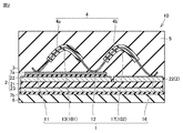
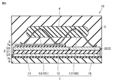
- FIG. 1 is a cross-sectional view schematically showing the configuration of the semiconductor device 10 according to the first embodiment.
- the height direction is used as a term indicating the direction.
- the height direction is a direction perpendicular to the circuit board 2.
- the semiconductor device 10 includes a bonding wire 1, a circuit board 2, a semiconductor element 3, a sealing material 4, a thermosetting resin 5, a base plate 6, and an upper bonding material 7a. And the lower bonding material 7b.
- the semiconductor device 10 is a power semiconductor device for electric power.
- a circuit board 2 is arranged on the base plate 6.
- the circuit board 2 is joined to the upper surface of the base plate 6 by the lower joining material 7.
- the material of the base plate 6 is, for example, copper (Cu) or a silicon carbide particle-reinforced aluminum composite material (AlSiC).
- the heat generated by the semiconductor element 3 is released to the outside by the base plate 6.
- the base plate 6 and the lower bonding material 7b may not be provided. When the base plate 6 and the lower bonding material 7b are not provided, the heat generated in the semiconductor device 10 is released to the outside by the lower conductor pattern 23 described later.
- the material of the upper bonding material 7a and the lower bonding material 7b is, for example, solder or a sinterable silver particle material.
- the circuit board 2 includes an insulating layer 21, an upper conductor pattern 22, and a lower conductor pattern 23.
- the insulating layer 21 is sandwiched between the upper conductor pattern 22 and the lower conductor pattern 23.
- the upper conductor pattern 22, the insulating layer 21, and the lower conductor pattern 23 are laminated in the order of the upper conductor pattern 22, the insulating layer 21, and the lower conductor pattern 23 in the height direction.
- the material of the insulating layer 21 is, for example, alumina (Al 2 O 3 ) or aluminum nitride (Al N). Further, when the base plate 6 and the lower bonding material 7b are not provided, the material of the insulating layer 21 may be a resin having an insulating property.
- the upper conductor pattern 22 is arranged on the upper surface of the insulating layer 21.
- the upper conductor pattern 22 is bonded to the semiconductor element 3 by the upper bonding material 7a.
- the lower conductor pattern 23 is arranged on the lower surface of the insulating layer 21.
- the lower conductor pattern 23 is joined to the upper surface of the base plate 6 by the lower bonding material 7b.
- the material of the upper conductor pattern 22 and the lower conductor pattern 23 is, for example, copper (Cu) or the like.
- Each of the upper conductor pattern 22 and the lower conductor pattern 23 may have a two-layer structure.
- Each of the upper conductor pattern 22 and the lower conductor pattern 23 is, for example, an aluminum (Al) layer formed on the surface of the insulating layer 21 and a copper (Cu) layer formed on the surface of the aluminum (Al) layer. And may be included.
- thermosetting resin 5 is arranged on the upper surface of the upper conductor pattern 22.
- the upper surface of the upper conductor pattern 22 may be provided with irregularities (not shown) by laser processing, a solvent, or the like. Further, the upper surface of the upper conductor pattern 22 may be coated with a coating (not shown) for improving the adhesion with the thermosetting resin 5. The unevenness or coating (not shown) prevents the thermosetting resin 5 from peeling off from the upper surface of the upper conductor pattern 22. Further, the lower surface of the lower conductor pattern 23 may also be provided with irregularities or coatings (not shown).
- the semiconductor element 3 is arranged on the circuit board 2.
- the semiconductor element 3 is bonded to the upper conductor pattern 22 by the upper bonding material 7a.
- the semiconductor element 3 may be, for example, a switching element such as an insulated gate type bipolar transistor (IGBT: Insulated Gate Bipolar Transistor) and a metal oxide semiconductor field effect transistor (MOSFET: Metal Oxide Semiconductor Field Effect Transistor), or a shot. It may be a rectifying element such as a key barrier diode.
- a surface electrode (not shown) is provided on the surface of the semiconductor element 3.
- the material of the surface electrode is, for example, aluminum (Al) or an aluminum alloy in which silicon (Si) is added to aluminum (Al).
- a coating layer (not shown) may be further provided on the surface of the surface electrode (not shown).
- the material of the coating layer (not shown) is, for example, nickel (Ni) or gold (Au).
- the material of the semiconductor element 3 is, for example, silicon (Si).
- the coefficient of linear expansion of the semiconductor element 3 formed of silicon (Si) is, for example, 3 ⁇ 10 -6 / K.
- the elastic modulus of the semiconductor element 3 formed of silicon (Si) is, for example, 70 GPa.
- the material of the semiconductor element 3 may be, for example, a wide bandgap semiconductor material having a bandgap larger than that of silicon (Si).
- the material of the semiconductor element 3 is preferably a wide bandgap semiconductor material. Wide bandgap semiconductor materials include, for example, silicon carbide (SiC), gallium nitride (GaN), diamond, and the like.
- the semiconductor element 3 formed of the wide bandgap semiconductor material has a higher allowable current density than the semiconductor element 3 formed of silicon (Si). Further, the power loss of the semiconductor element 3 formed of the wide bandgap semiconductor material is smaller than that of the semiconductor element 3 formed of silicon (Si). Therefore, by using a wide-gap semiconductor material as the material of the semiconductor element 3, the size of the semiconductor device 10 can be reduced.
- the upper limit of the operating temperature of the semiconductor element 3 formed of the wide bandgap semiconductor material is higher than that of the semiconductor element 3 formed of silicon (Si).
- the temperature of the semiconductor element 3 is high.
- the temperature of the semiconductor element 3 is, for example, 150 ° C. or higher.
- the temperature of the semiconductor element 3 is, for example, 200 ° C. or higher.
- the bonding wire 1 includes a first connecting portion 11, a second connecting portion 12, and a first loop portion 101.
- the first connection portion 11 is connected to the semiconductor element 3.
- the second connection portion 12 is connected to either the semiconductor element 3 or the circuit board 2.
- the first loop portion 101 is located between the first connection portion 11 and the second connection portion 12.
- the first loop portion 101 has a first bent portion 13.
- the second connection portion 12 is connected to the circuit board 2.
- the second connecting portion 12 may be connected to the semiconductor element 3.
- the bonding wire 1 is bonded to the semiconductor element 3 and the circuit board 2 by, for example, ultrasonic bonding.
- the bonding wire 1 electrically connects a surface electrode (not shown) of the semiconductor element 3 and the upper surface of the upper conductor pattern 22 of the circuit board 2.
- the bonding wire 1 is formed in a loop shape by the first loop portion 101.
- the first loop portion of the bonding wire is bent at the first bent portion 13.
- the first loop portion 101 projects upward with respect to the circuit board 2.
- the first loop portion 101 has a first portion 14 and a second portion 15.
- the first portion 14 connects the first connecting portion 11 and the first bent portion 13.
- the second portion 15 connects the second connecting portion 12 and the first bent portion 13.
- the first portion 14 extends in a direction intersecting the second portion 15.
- the first bent portion 13 is connected to the first portion 14 and the second portion 15.
- the first portion 14 and the second portion 15 face each other with the first bent portion 13 interposed therebetween.
- the first portion 14 and the second portion 15 may be exposed from the sealing material 4.
- the bonding wire 1 is sealed with a thermosetting resin 5.
- the bonding wire 1 is bound to the thermosetting resin 5.
- the first connecting portion 11 and the second connecting portion 12 are sealed with the thermosetting resin 5 while being exposed from the sealing material 4.
- the first bent portion 13 is sealed with a thermosetting resin 5 while being covered with a sealing material 4.
- the first bent portion 13 is not in direct contact with the thermosetting resin 5.
- the upper end of the bonding wire 1 is covered with a sealing material 4.
- the lower end of the bonding wire 1 is sealed with a thermosetting resin 5.
- the material of the bonding wire 1 is a conductive metal such as aluminum (Al) or copper (Cu).
- the coefficient of linear expansion of the bonding wire 1 is, for example, 2.3 ⁇ 10-5 / K.
- the elastic modulus of the bonding wire 1 is, for example, 70 GPa.
- the sealing material 4 covers the first bent portion 13 of the first loop portion 101.
- the sealing material 4 has a lower elastic modulus than the thermosetting resin 5.
- the sealing material 4 does not cover the first connecting portion 11 and the second connecting portion 12.
- the sealing material 4 is sealed with a thermosetting resin 5. Since the sealing material 4 has a lower elastic modulus than the thermosetting resin 5 and covers the first bent portion 13, it functions as a cushioning material for the first bent portion 13.
- the sealing material 4 may have a lower elastic modulus than the bonding wire 1.
- the shape of the sealing material 4 may be appropriately determined as long as the first bent portion 13 is covered.
- the sealing material 4 may have a shape along the first bent portion 13 as shown in FIG. 1, or may have a substantially spherical shape as shown in FIG. 7. ..
- the material of the sealing material 4 is different from the material of the thermosetting resin 5.
- the sealing material 4 is softer than the thermosetting resin 5. Inside the sealing material 4, the first bent portion 13 is deformable.
- the material of the sealing material 4 is, for example, polyimide.
- Polyimide generally has a lower elastic modulus than the epoxy resin which is the material of the thermosetting resin 5.
- Polyimide generally has higher strength and higher heat resistance than other polymer compounds.
- Polyimide has electrical insulating properties and is therefore used as an insulating material. From the above, the sealing material 4 has high strength, high heat resistance, and electrical insulation.
- the difference between the linear expansion coefficient of the sealing material 4 and the linear expansion coefficient of the bonding wire 1 may be smaller than the difference between the linear expansion coefficient of the thermosetting resin 5 and the linear expansion coefficient of the bonding wire 1.
- polyimide has a relatively low coefficient of linear expansion among organic substances.
- polyimide has a coefficient of linear expansion that is relatively close to that of metal among organic substances. Therefore, since the thermal strain of the sealing material 4 formed of polyimide and the thermal strain of the bonding wire 1 formed of metal are close to each other, thermal stress is unlikely to occur in the bonding wire 1.
- the sealing material 4 may be a liquid having a constant viscosity in an uncured state and a normal temperature state.
- the material of the sealing material 4 may be appropriately determined according to the bonding wire 1.
- the sealing material 4 includes the first sealing portion 4a and the second sealing portion 4b as shown in FIG. 2, the materials of the first sealing portion 4a and the second sealing portion 4b are different. You may be.
- a material in which a plurality of materials are appropriately combined may be used as the material of the sealing material 4.
- thermosetting resin 5 seals the circuit board 2, the semiconductor element 3, the bonding wire 1, and the sealing material 4. Specifically, the thermosetting resin 5 seals the first connection portion 11 and the second connection portion 12 of the bonding wire 1.
- the thermosetting resin 5 reinforces the first connection portion 11 and the second connection portion 12 by sealing the first connection portion 11 and the second connection portion 12.
- the thermosetting resin 5 sandwiches the sealing material 4 to seal the first bent portion 13.
- the thermosetting resin 5 has a higher elastic modulus than the sealing material 4. The deformation of the bonding wire 1 is suppressed inside the thermosetting resin 5.
- the thermosetting resin 5 has an insulating property.
- the material of the thermosetting resin 5 is, for example, an epoxy resin.
- the elastic modulus of the epoxy resin is, for example, 5 GPa.
- the thermosetting resin 5 has a coefficient of linear expansion different from that of the bonding wire 1.
- the coefficient of linear expansion of the epoxy resin is, for example, 2.0 ⁇ 10-5 / K.
- the temperature of the semiconductor device 10 becomes high during operation, for example, 200 ° C.
- the thermosetting resin 5 is formed of a resin having a low glass transition temperature, the elasticity of the thermosetting resin 5 may decrease due to the softening or deterioration of the thermosetting resin 5 due to the high temperature.
- the reinforcement of the first connection portion 11 and the second connection portion 12 by the thermosetting resin 5 is impaired, so that the reliability of the first connection portion 11 and the second connection portion 12 may decrease. Therefore, the material of the thermosetting resin 5 is preferably a material that is suppressed from deteriorating at a high temperature. In order to prevent the thermosetting resin 5 from deteriorating due to high temperature, it is desirable that the thermosetting resin 5 contains a metal or filler (not shown).
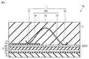
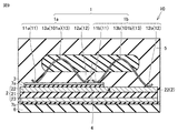
- the bonding wire 1 further includes a third connecting portion 16 and a second loop portion 102.
- the third connection portion 16 is connected to either the semiconductor element 3 or the circuit board 2.
- the second loop portion 102 is located between the second connecting portion 12 and the third connecting portion 16.
- the second loop portion 102 has a second bent portion 17.
- the second connecting portion 12 is connected to the semiconductor element 3, and the third connecting portion 16 is connected to the circuit board 2.
- the sealing material 4 covers each of the first bent portion 13 and the second bent portion 17.
- the sealing material 4 includes a first sealing portion 4a and a second sealing portion 4b.
- the first sealing portion 4a covers the first bent portion 13.
- the second sealing portion 4b covers the second bent portion 17.
- the first sealing portion 4a is separated from the second sealing portion 4b.
- the first sealing portion 4a and the second sealing portion 4b are separate bodies.
- the third connecting portion 16 is exposed from the sealing material 4.
- the heat generated in the semiconductor element 3 is dissipated by the following path shown in FIG. 1, so that the semiconductor device 10 is cooled. That is, the heat generated in the semiconductor element 3 moves in the order of the upper bonding material 7a, the upper conductor pattern 22, the insulating layer 21, the lower conductor pattern 23, the lower bonding material 7b, and the base plate 6, and the semiconductor from the base plate 6 The heat is dissipated to the outside of the device 10. As a result, the temperature of the semiconductor device 10 is lowered. Specifically, the temperature of the semiconductor element 3 drops sharply.
- Deformation occurs in the semiconductor device 10 due to changes in the temperature of the semiconductor device 10. Specifically, when the temperature of the semiconductor device 10 rises, the bonding wire 1, the sealing material 4, and the thermosetting resin 5 thermally expand. Further, when the temperature of the semiconductor device 10 decreases, the bonding wire 1, the sealing material 4, and the thermosetting resin 5 are thermally shrunk. As the temperature change (temperature swing) of the semiconductor device 10 increases, the amount of deformation of the semiconductor device 10 increases.
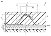
- FIG. 3 is a cross-sectional view showing the configuration of the semiconductor device 10 according to the comparative example.
- the semiconductor device 10 according to the comparative example does not include the sealing material 4. Therefore, the first bent portion 13 of the first loop portion 101 of the bonding wire 1 of the semiconductor device 10 according to the comparative example shown in FIG. 3 is sealed with the thermosetting resin 5. Therefore, in the comparative example, the deformation of the first bent portion 13 is hindered by the thermosetting resin 5.
- the thermal stress of the first portion 14 in the direction along the first portion 14 and the thermal stress of the second portion 15 in the direction along the second portion 15 Is generated in the first bent portion 13. That is, since the first bent portion 13 is bent, thermal stress in two different directions is generated in the first bent portion 13 as the temperature of the semiconductor device 10 changes. Therefore, thermal stress is concentrated on the first bent portion 13.
- the thermal stress generated in the first bent portion 13 is large, cracks may occur in the first bent portion 13.
- the crack can gradually develop by repeating the temperature change of the semiconductor device 10. If the crack grows, the bonding wire 1 can be shredded.
- the first bent portion 13 is a sealing material 4 having a lower elastic modulus than the thermosetting resin 5. It is covered. Therefore, the deformation of the first bent portion 13 is not hindered as compared with the comparative example. Therefore, the concentration of thermal stress on the first bent portion 13 is alleviated. Therefore, cracks are prevented from occurring in the first bent portion 13 and extending.
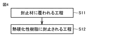
- the method for manufacturing the semiconductor device 10 includes a step S11 of being covered with the sealing material 4 and a step S12 of being sealed with the thermosetting resin 5.
- the step S11 covered with the sealing material 4 the first bent portion 13 of the first loop portion 101 of the bonding wire 1 is covered with the sealing material 4.
- the step S12 of sealing with the thermosetting resin 5 the circuit board 2, the semiconductor element 3, the bonding wire 1, and the sealing material 4 are sealed with the thermosetting resin 5.
- the bonding wire 1, the circuit board 2, the semiconductor element 3, the base plate 6, the upper bonding material 7a and the lower bonding material 7b shown in FIG. 1 are bonded by the following process.
- the upper conductor pattern 22 of the circuit board 2 is joined to the semiconductor element 3 by the upper bonding material 7a.
- the lower conductor pattern 23 of the circuit board 2 is joined to the base plate 6 by the lower bonding material 7b.
- the first connection portion 11 of the bonding wire 1 is bonded to the semiconductor element 3 by ultrasonic bonding.
- the second connecting portion 12 is bonded to the semiconductor element 3 or the circuit board 2 by ultrasonic bonding. In the present embodiment, the second connection portion 12 is joined to the circuit board 2.
- the bonding wire 1 may be bonded to the circuit board 2 and the semiconductor element 3 after the semiconductor element 3 and the base plate 6 are bonded to the circuit board 2.
- the semiconductor element 3 and the base plate 6 may be bonded to the circuit board 2 after the bonding wire 1 is bonded to the circuit board 2 and the semiconductor element 3.
- the sealing material 4 is applied by being dropped onto the bonding wire 1 by, for example, a dispenser or the like. As a result, as shown in FIG. 1, the first bent portion 13 of the first loop portion 101 of the bonding wire 1 is covered with the sealing material 4.
- the method of applying the sealing material 4 to the first bent portion 13 is not limited to a dispenser or the like.
- the sealing material 4 may be applied by immersing the first bent portion 13 in the sealing material 4.
- a container filled with the liquid sealing material 4 may be prepared and installed on a table or the like.
- the circuit board 2 to which the semiconductor element 3, the base plate 6, and the bonding wire 1 are bonded is held so that the bonding wire 1 is located below the circuit board 2. Only the first bent portion 13 of the first loop portion 101 of the bonding wire 1 of the circuit board 2 to which the semiconductor element 3, the base plate 6 and the bonding wire 1 are bonded is immersed in the container filled with the sealing material 4.
- the sealing material 4 is applied. After that, the circuit board 2 to which the semiconductor element 3, the base plate 6, and the bonding wire 1 are bonded is lifted. As a result, the bonding wire 1 in which the sealing material 4 is applied to the first bent portion 13 of the first loop portion 101 is obtained.
- the sealing material 4 is applied to the bonding wire 1 and then sealed in the thermosetting resin 5
- the circuit board 2, the semiconductor element 3, and the bonding wire 1 are as shown in FIG. ,
- the sealing material 4 is sealed in the thermosetting resin 5.
- the sealing material 4 covering the first bent portion 13 of the first loop portion 101 of the bonding wire 1 is made of a thermosetting resin 5. Also has a low elastic modulus. Therefore, the first bent portion 13 is more easily deformed inside the sealing material 4 than when the first bent portion 13 is sealed with the thermosetting resin 5. Therefore, the thermal stress generated in the first bent portion 13 can be reduced as compared with the case where the first bent portion 13 is sealed with the thermosetting resin 5. Therefore, the growth of cracks at the first bent portion 13 can be suppressed.
- the first connection portion 11 and the second connection portion 12 are heated. Stress can occur.
- the semiconductor device 10 of the present embodiment as shown in FIG. 1, the first connection portion 11 and the second connection portion 12 are sealed with a thermosetting resin 5. Thereby, the first connection portion 11 and the second connection portion 12 can be reinforced. Further, since the deformation generated in the first connection portion 11 and the second connection portion 12 is distributed in the thermosetting resin 5, it is possible to prevent the thermal stress from concentrating on the first connection portion 11 and the second connection portion 12. ..
- Wire lift-off means that the bonding wire 1 is separated from the semiconductor element 3 or the circuit board 2 due to the growth of cracks generated by the thermal stress repeatedly applied to the first connection portion 11 or the second connection portion 12 due to the temperature change. It is a phenomenon that occurs.
- the sealing material 4 When the material of the sealing material 4 is polyimide or the like having an insulating property, the sealing material 4 can also insulate the semiconductor device 10 and the outside of the semiconductor device 10 in the same manner as the thermosetting resin 5. Therefore, even when the sealing material 4 covers the bonding wire 1, it is possible to prevent the insulating property from being lowered.
- the respective materials of the sealing material 4 and the thermosetting resin 5 can be appropriately selected.
- the materials of the sealing material 4 and the thermosetting resin 5 can be optimally selected according to the required properties.
- the materials of the sealing material 4 and the thermosetting resin 5 have, for example, the presence or absence of insulation, the elastic modulus, the linear expansion coefficient, the heat dissipation, the shape of the first loop portion 101 of the adhesive strength, the curvature of the first bent portion 13, and the like. You can choose according to your needs.
- the difference between the linear expansion coefficient of the sealing material 4 and the linear expansion coefficient of the bonding wire 1 is smaller than the difference between the linear expansion coefficient of the thermosetting resin 5 and the linear expansion coefficient of the bonding wire 1.
- the materials of the material 4 and the thermosetting resin 5 can be selected. Thereby, the thermal stress generated in the bonding wire 1 can be reduced.
- the first bent portion 13 and the second bent portion 17 are respectively the first sealing portion 4a and the second sealing portion. Since it is covered by each of 4b, the material of the sealing material 4 can be selected according to the first bent portion 13 and the second bent portion 17. Therefore, the sealing material 4 can be optimally selected.
- the first bent portion 13 is covered with a sealing material 4 having an elastic modulus lower than that of the thermosetting resin 5, and then the thermosetting resin 5 is covered. Is sealed in. Therefore, the thermal stress generated in the first bent portion 13 can be reduced. As a result, the growth of cracks at the first bent portion 13 can be suppressed.
- Embodiment 2 Unless otherwise specified, the second embodiment has the same configuration, manufacturing method, and action and effect as those of the first embodiment. Therefore, the same components as those in the first embodiment are designated by the same reference numerals, and the description will not be repeated.
- FIG. 5 is a cross-sectional view schematically showing the configuration of the semiconductor device 10 according to the second embodiment.
- the sealing material 4 is located above the height position H, which is half the height from the first connecting portion 11 of the bonding wire 1 to the upper end of the first loop portion 101.
- the sealing material 4 is not located below the height position H, which is half the height from the first connecting portion 11 to the upper end of the first loop portion 101.
- a part of the sealing material 4 is located above the height of the upper end of the first loop portion 101.
- the first bent portion 13 is located above the height position H, which is half the height from the first connecting portion 11 to the upper end of the first loop portion 101.
- the first connection portion 11 and the second connection portion 12 are located below the height position H, which is half the height from the first connection portion 11 to the upper end of the first loop portion 101.
- At least a part of the upper half of the first loop portion 101 is covered with the sealing material 4.
- the lower half of the first loop portion 101 is not covered with the sealing material 4.
- the first bent portion 13 has a radius of curvature larger than 2 mm.
- the first bent portion 13 may have a first major bent portion 131 and a second major bent portion 132.
- the first major bending portion 131 and the second major bending portion 132 are connected by a third portion 18 of the first loop portion 101.
- the first portion 14, the second portion 15, and the third portion 18 have, for example, a radius of curvature of 2 mm or less.
- the first bent portion 13 has a radius of curvature larger than that of the first portion 14, the second portion 15, and the third portion 18.
- the sealing material 4 has a third sealing portion 4c and a fourth sealing portion 4d.
- the sealing material 4 covers only the portion of the first loop portion 101 having a large radius of curvature. Specifically, the third sealing portion 4c covers the first large bending portion 131.
- the fourth sealing portion 4d covers the second large bending portion 132.
- the sealing material 4 is above the half height position H from the first connecting portion 11 to the upper end of the first loop portion 101. Since it is located at and not below the height position H, the amount of the sealing material 4 contained in the semiconductor device 10 can be reduced. Therefore, the manufacturing cost of the semiconductor device 10 can be reduced.
- the sealing material 4 since the first bent portion 13 has a radius of curvature larger than 2 mm, the sealing material 4 has a radius of curvature smaller than 2 mm. It does not cover the portion of the first loop portion 101. Therefore, the amount of the sealing material 4 contained in the semiconductor device 10 can be further reduced. Therefore, the manufacturing cost of the semiconductor device 10 can be reduced. In addition, in order to obtain the advantageous effect in the present embodiment, it is necessary to appropriately control the amount of the sealing material 4 applied to the first bent portion 13.
- Embodiment 3 Unless otherwise specified, the third embodiment has the same configuration, manufacturing method, and action and effect as those of the first embodiment. Therefore, the same components as those in the first embodiment are designated by the same reference numerals, and the description will not be repeated.
- FIG. 7 is a cross-sectional view schematically showing the configuration of the semiconductor device 10 according to the third embodiment.
- the sealing material 4 fills a region between the first bent portion 13 and at least one of the semiconductor element 3 and the circuit board 2, and is in contact with at least one of the semiconductor element 3 and the circuit board 2.
- the sealing material 4 fills the region between the first bent portion 13 and the semiconductor element 3 and the circuit board 2, and is in contact with both the semiconductor element 3 and the circuit board 2.
- the sealing material 4 integrally covers the first bent portion 13 and at least a part of at least one of the semiconductor element 3 and the circuit board 2.
- the sealing material 4 is adhered to at least one of the semiconductor element 3 and the circuit board 2.
- the material of the sealing material 4 needs to have an insulating property.
- the sealing material 4 may cover the first loop portion 101 except for the vicinity of the first connecting portion 11 and the second connecting portion 12.
- the first bent portion 13 is covered with the sealing material 4. Further, the region between the first bent portion 13 and at least one of the semiconductor element 3 and the circuit board 2 is filled with the sealing material 4. Further, the sealing material 4 is arranged so as to be in contact with at least one of the semiconductor element 3 and the circuit board 2. The sealing material 4 is dropped so as to fill a region between the first bent portion 13 and at least one of the semiconductor element 3 and the circuit board 2.
- the sealing material 4 fills the region between the first bent portion 13 and at least one of the semiconductor element 3 and the circuit board 2. It is arranged so as to be in contact with at least one of the semiconductor element 3 and the circuit board 2. Therefore, the amount of the sealing material 4 is larger than that in the case where the sealing material 4 is applied only to the first bent portion 13. The permissible variation in the amount of the sealing material 4 applied is large. Therefore, the amount of the sealing material 4 applied does not need to be strictly controlled. Therefore, since the manufacturing method of the semiconductor device 10 is simplified, the manufacturing cost of the semiconductor device 10 can be reduced.
- Embodiment 4 Unless otherwise specified, the fourth embodiment has the same configuration, manufacturing method, and action and effect as those of the first embodiment. Therefore, the same components as those in the first embodiment are designated by the same reference numerals, and the description will not be repeated.
- the sealing material 4 integrally covers the first bent portion 13 of the first loop portion 101 and the second bent portion 17 of the second loop portion 102.
- the material of the sealing material 4 has an insulating property.
- the bonding wire 1 includes a plurality of loop portions.
- the bonding wire 1 includes a plurality of wire portions. Specifically, the bonding wire 1 includes a first wire portion 1a and a second wire portion 1b.
- the first bent portion 13 has a first wire portion bent portion 13a and a second wire portion bent portion 13b.
- the first wire portion bent portion 13a is included in the first wire portion 1a.
- the second wire portion bent portion 13b is included in the second wire portion 1b.
- the sealing material 4 integrally covers the first wire portion bent portion 13a and the second wire portion bent portion 13b.
- the first wire portion 1a is electrically connected to the second wire portion 1b.
- the first wire portion 1a has a first wire portion loop portion 101a.
- the second wire portion 1b has a second wire portion loop portion 101b.
- the first connection portion 11 has a first wire portion first connection portion 11a and a second wire portion first connection portion 11b.
- the second connection portion 12 has a first wire portion second connection portion 12a and a second wire portion second connection portion 12b.
- the first wire portion first connection portion 11a and the first wire portion second connection portion 12a are included in the first wire portion 1a.
- the second wire portion first connection portion 11b and the second wire portion second connection portion 12b are included in the second wire portion 1b.
- the first wire portion bent portion 13a is included in the first wire portion loop portion 101a located between the first wire portion first connection portion 11a and the first wire portion second connection portion 12a.
- the second wire portion bent portion 13b is included in the second wire portion loop portion 101b located between the second wire portion first connection portion 11b and the second wire portion second connection portion 12b.
- the sealing material 4 forms the first bent portion 13 of the first loop portion 101 and the second bent portion 17 of the second loop portion 102. Since it is integrally covered, the first bent portion 13 and the second bent portion 17 can be simultaneously covered by the sealing material 4 in the step S11 covered by the sealing material 4. Therefore, the manufacturing process can be simplified as compared with the case where each of the first bent portion 13 and the second bent portion 17 is individually covered. Therefore, even when the bonding wire 1 includes a plurality of loop portions, the manufacturing cost of the semiconductor device 10 can be reduced.
- the bonding wire 1 integrally covers the first wire portion bent portion 13a and the second wire portion bent portion 13b. Therefore, in the step S11 covered by the sealing material 4, the first wire portion bent portion 13a and the second wire portion bent portion 13b can be simultaneously covered by the sealing material 4. Therefore, the manufacturing process can be simplified as compared with the case where each of the first wire portion bent portion 13a and the second wire portion bent portion 13b is individually covered. Therefore, even when the bonding wire 1 has a plurality of wire portions, the manufacturing cost of the semiconductor device 10 can be reduced.
- Embodiment 5 the semiconductor devices according to the above-described first to fourth embodiments are applied to a power conversion device.
- the present invention is not limited to a specific power conversion device, the case where the present invention is applied to a three-phase inverter will be described below as a fifth embodiment.
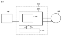
- FIG. 10 is a block diagram showing a configuration of a power conversion system to which the power conversion device according to the present embodiment is applied.
- the power conversion system shown in FIG. 10 includes a power supply 100, a power conversion device 200, and a load 300.
- the power supply 100 is a DC power supply, and supplies DC power to the power converter 200.
- the power supply 100 can be configured with various things, for example, it can be configured with a DC system, a solar cell, a storage battery, or it can be configured with a rectifier circuit or an AC / DC converter connected to an AC system. May be good.
- the power supply 100 may be configured by a DC / DC converter that converts the DC power output from the DC system into a predetermined power.
- the power conversion device 200 is a three-phase inverter connected between the power supply 100 and the load 300, converts the DC power supplied from the power supply 100 into AC power, and supplies AC power to the load 300. As shown in FIG. 10, the power conversion device 200 has a main conversion circuit 201 that converts DC power into AC power and outputs it, and a control circuit 203 that outputs a control signal for controlling the main conversion circuit 201 to the main conversion circuit 201. And have.
- the load 300 is a three-phase electric motor driven by AC power supplied from the power converter 200.
- the load 300 is not limited to a specific application, and is an electric motor mounted on various electric devices.
- the load 300 is used as an electric motor for a hybrid vehicle, an electric vehicle, a railroad vehicle, an elevator, or an air conditioner.
- the main conversion circuit 201 includes a switching element and a freewheeling diode (not shown), and when the switching element switches, the DC power supplied from the power supply 100 is converted into AC power and supplied to the load 300.
- the main conversion circuit 201 is a two-level three-phase full bridge circuit, and has six switching elements and each switching element. It can consist of six anti-parallel freewheeling diodes.
- Each switching element and each freewheeling diode of the main conversion circuit 201 are configured by a semiconductor module 202 corresponding to any one of the above-described first to fourth embodiments.
- the six switching elements are connected in series for each of the two switching elements to form an upper and lower arm, and each upper and lower arm constitutes each phase (U phase, V phase, W phase) of the full bridge circuit. Then, the output terminals of the upper and lower arms, that is, the three output terminals of the main conversion circuit 201 are connected to the load 300.
- the main conversion circuit 201 includes a drive circuit (not shown) for driving each switching element
- the drive circuit may be built in the semiconductor module 202, or a drive circuit may be provided separately from the semiconductor module 202. It may be provided.
- the drive circuit generates a drive signal for driving the switching element of the main conversion circuit 201 and supplies the drive signal to the control electrode of the switching element of the main conversion circuit 201.
- a drive signal for turning on the switching element and a drive signal for turning off the switching element are output to the control electrodes of each switching element.
- the drive signal When the switching element is kept on, the drive signal is a voltage signal (on signal) equal to or higher than the threshold voltage of the switching element, and when the switching element is kept off, the drive signal is a voltage equal to or lower than the threshold voltage of the switching element. It becomes a signal (off signal).
- the control circuit 203 controls the switching element of the main conversion circuit 201 so that the desired power is supplied to the load 300. Specifically, the time (on time) at which each switching element of the main conversion circuit 201 should be in the on state is calculated based on the power to be supplied to the load 300.
- the main conversion circuit 201 can be controlled by PWM control that modulates the on-time of the switching element according to the voltage to be output. Then, a control command (control signal) is output to the drive circuit included in the main conversion circuit 201 so that an on signal is output to the switching element that should be turned on at each time point and an off signal is output to the switching element that should be turned off. Is output.
- the drive circuit outputs an on signal or an off signal as a drive signal to the control electrode of each switching element according to this control signal.
- the semiconductor module according to the first to fourth embodiments is applied as the switching element of the main conversion circuit 201 and the freewheeling diode, cracks occur at the first bent portion of the bonding wire and cracks occur. The progress can be suppressed.
- the present invention is not limited to this, and can be applied to various power conversion devices.
- a two-level power conversion device is used, but a three-level or multi-level power conversion device may be used. You may apply it.
- the present invention can be applied to a DC / DC converter or an AC / DC converter.
- the power conversion device to which the present invention is applied is not limited to the case where the above-mentioned load is an electric motor, and is, for example, a power supply device for a discharge machine, a laser machine, an induction heating cooker, or a non-contact power supply system. It can also be used as a power conditioner for a photovoltaic power generation system, a power storage system, or the like.
- thermosetting resin 10 semiconductor device, 11 1st connection part, 12 2nd connection part , 13 1st bent part, 13a 1st wire part bent part, 13b 2nd wire part bent part, 16 3rd connection part, 17 2nd bent part, 100 power supply, 101 1st loop part, 102 2nd loop part, 200 power converter, 201 main conversion circuit, 202 semiconductor module, 203 circuit board, 300 load, H height position.
Landscapes
- Engineering & Computer Science (AREA)
- Microelectronics & Electronic Packaging (AREA)
- Power Engineering (AREA)
- Physics & Mathematics (AREA)
- Condensed Matter Physics & Semiconductors (AREA)
- General Physics & Mathematics (AREA)
- Computer Hardware Design (AREA)
- Structures Or Materials For Encapsulating Or Coating Semiconductor Devices Or Solid State Devices (AREA)
Abstract
半導体装置(10)は、回路基板(2)と、半導体素子(3)と、ボンディングワイヤ(1)と、封止材(4)と、熱硬化性樹脂(5)とを備えている。半導体素子(3)は、回路基板(4)に配置されている。ボンディングワイヤ(1)は、第1接続部(11)と、第2接続部(12)と、第1ループ部(101)とを含んでいる。第1接続部(11)は、半導体素子(3)と接続されている。第2接続部(12)は、半導体素子(3)および回路基板(4)のいずれかと接続されている。第1ループ部(101)は、第1接続部(11)と第2接続部(12)との間に位置し、第1屈曲部(13)を有している。封止材(4)は、第1屈曲部(14)を覆っている。熱硬化性樹脂(5)は、回路基板(2)と、半導体素子(3)と、ボンディングワイヤ(1)と、封止材(4)とを封止し、かつ熱硬化性樹脂(5)よりも低い弾性率を有している。
Description
本発明は、半導体装置、電力変換装置および半導体装置の製造方法に関するものである。
従来、半導体装置は、半導体素子と回路基板とを接続するためのボンディングワイヤと、半導体素子、回路基板およびボンディングワイヤを封止する熱硬化性樹脂とを備えている。例えば、特開平8-288426号公報(特許文献1)には、半導体素子、回路基板およびボンディングワイヤが熱硬化性樹脂により封止された半導体装置が記載されている。この公報に記載された半導体装置では、ボンディングワイヤは、半導体素子と接続されている第1接続部と、回路基板と接続されている第2接続部と、第1接続部と第2接続部との間に位置するループ部とを含んでいる。また、半導体装置は、第2接続部を覆う封止材(ワイヤ固定樹脂)をさらに備えている。
上記公報に掲載された半導体装置においては、第1接続部が熱硬化性樹脂によって封止され、かつ第2接続部が封止材によって覆われていることにより、第1接続部および第2接続部においてクラックが進展することが抑制されている。一方で、上記公報に掲載された半導体装置の動作中に半導体素子が発熱することにより、ボンディングワイヤおよび熱硬化性樹脂の温度が変化する。ボンディングワイヤは、ボンディングワイヤと異なる線膨張係数を有する熱硬化性樹脂によって封止されている。そのため、ボンディングワイヤが温度変化に伴って変形することが妨げられている。このため、ボンディングワイヤには熱応力が発生する。また、ループ部は屈曲部において屈曲しているため、屈曲部には熱応力が集中して発生する。よって、屈曲部においてクラックが発生し、進展し得る。
本発明は上記課題に鑑みてなされたものであり、その目的は、ボンディングワイヤの第1接続部および第2接続部でのクラックの進展を抑制できるとともに、屈曲部でのクラックの進展を抑制できる半導体装置を提供することである。
本発明の半導体装置は、回路基板と、半導体素子と、ボンディングワイヤと、封止材と、熱硬化性樹脂とを備えている。半導体素子は、回路基板に配置されている。ボンディングワイヤは、第1接続部と、第2接続部と、第1ループ部とを含んでいる。第1接続部は、半導体素子と接続されている。第2接続部は、半導体素子および回路基板のいずれかと接続されている。第1ループ部は、第1接続部と第2接続部との間に位置している。第1ループ部は、第1屈曲部を有している。封止材は、第1屈曲部を覆っている。熱硬化性樹脂は、回路基板と、半導体素子と、ボンディングワイヤと、封止材とを封止している。封止材は、熱硬化性樹脂よりも低い弾性率を有している。
本発明の半導体装置によれば、第1屈曲部を覆う封止材は、熱硬化性樹脂よりも低い弾性率を有している。このため、第1屈曲部が熱硬化性樹脂に封止されている場合よりも第1屈曲部に発生する熱応力を低減させることができる。よって、第1屈曲部でのクラックの進展を抑制できる。また、第1接続部および第2接続部が熱硬化性樹脂に封止されているため、第1接続部および第2接続部でのクラックの進展を抑制できる。
以下、本発明の実施の形態について図に基づいて説明する。なお、以下では、同一または相当する部分に同一の符号を付すものとし、重複する説明は繰り返さない。
実施の形態1.
〈半導体装置10の構成について〉
図1~図3を用いて、実施の形態1に係る半導体装置10の構成を説明する。図1は、本実施の形態1に係る半導体装置10の構成を概略的に示す断面図である。
〈半導体装置10の構成について〉
図1~図3を用いて、実施の形態1に係る半導体装置10の構成を説明する。図1は、本実施の形態1に係る半導体装置10の構成を概略的に示す断面図である。
本願では方向を示す用語として、高さ方向が用いられる。高さ方向とは、回路基板2に対して垂直な方向である。
図1に示されるように、半導体装置10は、ボンディングワイヤ1と、回路基板2と、半導体素子3と、封止材4と、熱硬化性樹脂5と、ベース板6と、上側接合材7aと、下側接合材7bとを含んでいる。半導体装置10は、電力用のパワー半導体装置である。
図1に示されるように、ベース板6には回路基板2が配置されている。回路基板2は、下側接合材7によってベース板6の上面に接合されている。ベース板6の材料は、例えば、銅(Cu)または炭化珪素粒子強化アルミニウム複合材(AlSiC)などである。半導体素子3で発生した熱は、ベース板6によって外部に放出される。なお、ベース板6および下側接合材7bは、設けられていなくてもよい。ベース板6および下側接合材7bが設けられていない場合、半導体装置10で発生した熱は、後述する下側導体パターン23によって外部に放出される。上側接合材7aおよび下側接合材7bの材料は、例えば、はんだまたは焼結性銀粒子材などである。
図1に示されるように、回路基板2は、絶縁層21と、上側導体パターン22と、下側導体パターン23とを含んでいる。絶縁層21は、上側導体パターン22と下側導体パターン23とによって挟み込まれている。上側導体パターン22と、絶縁層21と、下側導体パターン23とは、高さ方向に上側導体パターン22、絶縁層21、下側導体パターン23の順で積層されている。絶縁層21の材料は、例えば、アルミナ(Al2O3)または窒化アルミニウム(AlN)などである。また、ベース板6および下側接合材7bが設けられていない場合、絶縁層21の材料は、絶縁性を有している樹脂であってもよい。
上側導体パターン22は、絶縁層21の上面に配置されている。上側導体パターン22は、上側接合材7aによって半導体素子3と接合されている。下側導体パターン23は、絶縁層21の下面に配置されている。下側導体パターン23は、下側接合材7bによってベース板6の上面と接合されている。上側導体パターン22および下側導体パターン23の材料は、例えば、銅(Cu)などである。上側導体パターン22および下側導体パターン23のそれぞれは、二層構造であってもよい。上側導体パターン22および下側導体パターン23のそれぞれは、例えば、絶縁層21の表面に形成されているアルミニウム(Al)層と、アルミニウム(Al)層の表面に形成されている銅(Cu)層とを含んでいてもよい。
上側導体パターン22の上面には、熱硬化性樹脂5との界面が配置されている。上側導体パターン22の上面には、レーザー加工または溶剤などによって図示されない凹凸が設けられていてもよい。また、上側導体パターン22の上面には、熱硬化性樹脂5との密着性を向上させるための図示されないコーティングが施されていてもよい。図示されない凹凸またはコーティングによって、上側導体パターン22の上面から熱硬化性樹脂5が剥離することが抑制されている。また、下側導体パターン23の下面にも、図示されない凹凸またはコーティングが設けられていてもよい。
図1に示されるように、半導体素子3は、回路基板2に配置されている。半導体素子3は、上側接合材7aによって、上側導体パターン22に接合されている。半導体素子3は、例えば、絶縁ゲート型バイポーラトランジスタ(IGBT:Insulated Gate Bipolar Transistor)および金属酸化物半導体電界効果トランジスタ(MOSFET:Metal Oxide Semiconductor Field Effect Transistor)などのスイッチング素子であってもよいし、ショットキーバリアダイオードなどの整流素子であってもよい。
半導体素子3の表面には、図示されない表面電極が設けられている。表面電極の材料は、例えば、アルミニウム(Al)、またはアルミニウム(Al)に珪素(Si)が添加されたアルミニウム合金などである。図示されない表面電極の表面には、図示されない被覆層がさらに設けられていてもよい。図示されない被覆層の材料は、例えば、ニッケル(Ni)または金(Au)などである。
半導体素子3の材料は、例えば、珪素(Si)である。珪素(Si)によって形成されている半導体素子3の線膨張係数は、例えば、3×10⁻⁶/Kである。珪素(Si)によって形成されている半導体素子3の弾性率は、例えば、70GPaである。半導体素子3の材料は、例えば、珪素(Si)よりも大きいバンドギャップを有しているワイドバンドギャップ半導体材料であってもよい。半導体素子3の材料は、望ましくは、ワイドバンドギャップ半導体材料である。ワイドバンドギャップ半導体材料は、例えば、炭化珪素(SiC)、窒化ガリウム(GaN)またはダイヤモンドなどである。
ワイドバンドギャップ半導体材料によって形成されている半導体素子3は、珪素(Si)によって形成されている半導体素子3よりも、高い許容電流密度を有している。また、ワイドバンドギャップ半導体材料によって形成されている半導体素子3の電力損失は、珪素(Si)によって形成されている半導体素子3よりも小さい。このため、半導体素子3の材料としてワイドギャップ半導体材料が用いられることで、半導体装置10の寸法を小さくすることができる。
ワイドバンドギャップ半導体材料によって形成されている半導体素子3の動作温度の上限は、珪素(Si)によって形成されている半導体素子3よりも高い。例えば、炭化珪素(SiC)によって形成されている半導体素子3を含んでいる半導体装置10が動作する場合、半導体素子3の温度は、高温である。この場合、半導体素子3の温度は、例えば、150℃以上である。この場合、半導体素子3の温度は、例えば、200℃以上である。
図1に示されるように、ボンディングワイヤ1は、第1接続部11と、第2接続部12と、第1ループ部101とを含んでいる。第1接続部11は、半導体素子3と接続されている。第2接続部12は、半導体素子3および回路基板2のいずれかと接続されている。第1ループ部101は、第1接続部11と第2接続部12との間に位置している。第1ループ部101は、第1屈曲部13を有している。本実施の形態においては、第2接続部12は、回路基板2と接続されている。図2に示されるように、第2接続部12は、半導体素子3と接続されていてもよい。
ボンディングワイヤ1は、例えば、超音波接合によって半導体素子3および回路基板2に接合されている。ボンディングワイヤ1は、半導体素子3の図示されない表面電極と、回路基板2の上側導体パターン22の上面とを電気的に接続している。
図1に示されるように、ボンディングワイヤ1は、第1ループ部101によってループ状に形成されている。ボンディングワイヤの第1ループ部は、第1屈曲部13において屈曲している。第1ループ部101は、回路基板2に対して上側に突出している。
図1に示されるように、第1ループ部101は、第1部分14および第2部分15を有している。第1部分14は、第1接続部11と第1屈曲部13とを接続している。第2部分15は、第2接続部12と第1屈曲部13とを接続している。第1部分14は、第2部分15と交差する方向に延伸している。第1屈曲部13は、第1部分14および第2部分15と繋がっている。第1部分14および第2部分15は、第1屈曲部13を挟んで互いに向かい合っている。第1部分14および第2部分15は、封止材4から露出していてもよい。
図1に示されるように、ボンディングワイヤ1は、熱硬化性樹脂5に封止されている。ボンディングワイヤ1は、熱硬化性樹脂5に拘束されている。第1接続部11および第2接続部12は、封止材4から露出しつつ、熱硬化性樹脂5に封止されている。第1屈曲部13は、封止材4に覆われつつ、熱硬化性樹脂5に封止されている。第1屈曲部13は、熱硬化性樹脂5と直接に接触していない。ボンディングワイヤ1の上端は、封止材4に覆われている。ボンディングワイヤ1の下端は、熱硬化性樹脂5に封止されている。
ボンディングワイヤ1の材料は、例えば、アルミニウム(Al)または銅(Cu)などの導電性を有する金属である。ボンディングワイヤ1の材料がアルミニウム(Al)である場合、ボンディングワイヤ1の線膨張係数は、例えば、2.3×10⁻⁵/Kである。ボンディングワイヤ1の材料がアルミニウム(Al)である場合、ボンディングワイヤ1の弾性率は、例えば、70GPaである。
図1に示されるように、封止材4は、第1ループ部101の第1屈曲部13を覆っている。封止材4は、熱硬化性樹脂5よりも低い弾性率を有している。封止材4は、第1接続部11および第2接続部12を覆っていない。封止材4は、熱硬化性樹脂5に封止されている。封止材4は、熱硬化性樹脂5よりも低い弾性率を有しており、かつ第1屈曲部13を覆っているため、第1屈曲部13の緩衝材として機能している。封止材4は、ボンディングワイヤ1よりも低い弾性率を有していてもよい。封止材4の形状は、第1屈曲部13が覆われる限り適宜に決められてもよい。封止材4は、例えば、図1に示されるように第1屈曲部13に沿う形状を有していてもよいし、図7に示されるように略球状の形状を有していてもよい。
封止材4の材料は、熱硬化性樹脂5の材料と異なっている。封止材4は、熱硬化性樹脂5よりも柔らかい。封止材4の内部において、第1屈曲部13は変形可能である。封止材4の材料は、例えば、ポリイミドなどである。ポリイミドは、一般的に、熱硬化性樹脂5の材料であるエポキシ樹脂よりも低い弾性率を有している。ポリイミドは、一般的に、他の高分子化合物よりも高い強度および高い耐熱性を有している。ポリイミドは、電気絶縁性を有しているため、絶縁材料として用いられている。以上より、封止材4は、高い強度、高い耐熱性および電気絶縁性を有している。
封止材4の線膨張係数とボンディングワイヤ1の線膨張係数との差は、熱硬化性樹脂5の線膨張係数とボンディングワイヤ1の線膨張係数との差よりも小さくてもよい。例えば、ポリイミドは、有機物の中では相対的に低い線膨張係数を有している。このため、ポリイミドは、有機物の中では相対的に、金属と近い線膨張係数を有している。よって、ポリイミドによって形成されている封止材4の熱ひずみと金属によって形成されているボンディングワイヤ1の熱ひずみとが近いため、ボンディングワイヤ1に熱応力が生じにくい。
封止材4は、硬化されていない状態かつ常温の状態において、一定の粘度を有している液体であってもよい。これにより、後述される半導体装置10の製造方法において、封止材4がディスペンサなどによってボンディングワイヤ1の第1ループ部101に滴下された際に、第1屈曲部13のみに封止材4が塗布され得る。
封止材4の材料は、ボンディングワイヤ1に応じて適宜に決められてもよい。例えば、図2に示されるように封止材4が第1封止部4aおよび第2封止部4bを含んでいる場合、第1封止部4aおよび第2封止部4bの材料が異なっていてもよい。例えば、複数の材料が適宜に組み合わせられたものが封止材4の材料として用いられてもよい。
図1に示されるように、熱硬化性樹脂5は、回路基板2と、半導体素子3と、ボンディングワイヤ1と、封止材4とを封止している。熱硬化性樹脂5は、具体的には、ボンディングワイヤ1の第1接続部11および第2接続部12を封止している。熱硬化性樹脂5は、第1接続部11および第2接続部12を封止することによって第1接続部11および第2接続部12を補強している。熱硬化性樹脂5は、封止材4を挟み込んで、第1屈曲部13を封止している。
熱硬化性樹脂5は、封止材4よりも高い弾性率を有している。熱硬化性樹脂5の内部において、ボンディングワイヤ1が変形することが抑制されている。熱硬化性樹脂5は、絶縁性を有している。熱硬化性樹脂5の材料は、例えば、エポキシ樹脂などである。エポキシ樹脂の弾性率は、例えば、5GPaである。熱硬化性樹脂5は、ボンディングワイヤ1と異なる線膨張係数を有している。エポキシ樹脂の線膨張係数は、例えば、2.0×10⁻⁵/Kである。
半導体装置10の温度は動作時において、高温になり、例えば、200℃になる。仮に、熱硬化性樹脂5がガラス転移温度の低い樹脂によって形成されている場合、高温によって熱硬化性樹脂5が軟化または劣化をすることで、熱硬化性樹脂5の弾性が低下し得る。これにより、熱硬化性樹脂5による第1接続部11および第2接続部12の補強が損なわれるため、第1接続部11および第2接続部12の信頼性が低下し得る。このため、熱硬化性樹脂5の材料は、望ましくは、高温において劣化することが抑制されている材料である。熱硬化性樹脂5が高温によって劣化することが抑制されるために、熱硬化性樹脂5が図示されない金属またはフィラーなどを含んでいることが望ましい。
次に、図2を用いて、実施の形態1の変形例に係る半導体装置10の構成を説明する。実施の形態1の変形例において、ボンディングワイヤ1は、第3接続部16と、第2ループ部102とをさらに含んでいる。第3接続部16は、半導体素子3および回路基板2のいずれかと接続されている。第2ループ部102は、第2接続部12と第3接続部16との間に位置している。第2ループ部102は、第2屈曲部17を有している。実施の形態1の変形例において、第2接続部12は半導体素子3に接続され、第3接続部16は回路基板2に接続されている。
図2に示されるように、封止材4は、第1屈曲部13および第2屈曲部17のそれぞれを覆っている。封止材4は、第1封止部4aおよび第2封止部4bを含んでいる。第1封止部4aは、第1屈曲部13を覆っている。第2封止部4bは、第2屈曲部17を覆っている。第1封止部4aは、第2封止部4bと分離している。第1封止部4aおよび第2封止部4bは、別体である。第3接続部16は、封止材4から露出している。
〈半導体装置10の温度変化および温度変化に伴う変形および熱応力について〉
半導体装置10が動作している際に、半導体素子3は発熱している。このため、半導体装置10の温度は、上昇する。具体的には、図1に示される、第1接続部11および第2接続部12の近傍の温度は、特に上昇する。
半導体装置10が動作している際に、半導体素子3は発熱している。このため、半導体装置10の温度は、上昇する。具体的には、図1に示される、第1接続部11および第2接続部12の近傍の温度は、特に上昇する。
半導体装置10が動作を停止した後には、半導体素子3において発生した熱が、図1に示される、以下の経路によって放熱されることによって、半導体装置10が冷却される。すなわち、半導体素子3において発生した熱は、上側接合材7a、上側導体パターン22、絶縁層21、下側導体パターン23、下側接合材7b、ベース板6の順に移動し、ベース板6から半導体装置10の外部へと放熱される。これにより、半導体装置10の温度は、低下する。具体的には、半導体素子3の温度は、急激に低下する。
半導体装置10の温度が変化することによって、半導体装置10には変形が発生する。具体的には、半導体装置10の温度が上昇する場合には、ボンディングワイヤ1、封止材4および熱硬化性樹脂5が熱膨張する。また、半導体装置10の温度が低下する場合には、ボンディングワイヤ1、封止材4および熱硬化性樹脂5が熱収縮する。半導体装置10の温度変化(温度スイング)が大きくなるにつれて、半導体装置10の変形量が大きくなる。
図3は、比較例に係る半導体装置10の構成を示す断面図である。比較例に係る半導体装置10は、封止材4を含んでいない。このため、図3に示される比較例に係る半導体装置10のボンディングワイヤ1の第1ループ部101の第1屈曲部13は、熱硬化性樹脂5に封止されている。このため比較例において、第1屈曲部13の変形は、熱硬化性樹脂5によって妨げられている。
図3に示されるように、半導体装置10の温度変化に伴う半導体装置10の部材の変形が妨げられている場合、半導体装置10の部材には熱応力が発生する。具体的には、ボンディングワイヤ1は、ボンディングワイヤ1と異なる線膨張係数を有している熱硬化性樹脂5に封止されているため、半導体装置10の温度が変化した場合において変形することが妨げられている。このため、半導体装置10の温度が変化した場合、ボンディングワイヤ1には熱応力が発生する。
半導体装置10の温度が変化した場合、第1ループ部101において、第1部分14による第1部分14に沿う方向への熱応力および第2部分15による第2部分15に沿う方向への熱応力が第1屈曲部13に発生する。すなわち、第1屈曲部13が屈曲しているため、半導体装置10の温度変化に伴って、第1屈曲部13に2つの異なる方向への熱応力が発生する。よって、第1屈曲部13には、集中して熱応力が発生する。
第1屈曲部13に発生する熱応力が大きい場合、第1屈曲部13にクラックが発生し得る。クラックは、半導体装置10の温度変化が繰り返されることにより、徐々に進展し得る。クラックが進展した場合、ボンディングワイヤ1が寸断され得る。
一方で、図1に示されるように、本実施の形態に係る半導体装置10においては、第1屈曲部13は、熱硬化性樹脂5よりも低い弾性率を有している封止材4に覆われている。このため、第1屈曲部13の変形は、比較例よりも妨げられていない。よって、第1屈曲部13に熱応力が集中することが緩和されている。したがって、第1屈曲部13にクラックが発生し、進展することが抑制されている。
〈半導体装置10の製造方法について〉
次に、図4を参照して本実施の形態に係る半導体装置10の製造方法を説明する。半導体装置10の製造方法は、封止材4に覆われる工程S11と、熱硬化性樹脂5に封止される工程S12とを含んでいる。封止材4に覆われる工程S11において、ボンディングワイヤ1の第1ループ部101の第1屈曲部13が封止材4に覆われる。熱硬化性樹脂5に封止される工程S12において、回路基板2と、半導体素子3と、ボンディングワイヤ1と、封止材4とが、熱硬化性樹脂5に封止される。
次に、図4を参照して本実施の形態に係る半導体装置10の製造方法を説明する。半導体装置10の製造方法は、封止材4に覆われる工程S11と、熱硬化性樹脂5に封止される工程S12とを含んでいる。封止材4に覆われる工程S11において、ボンディングワイヤ1の第1ループ部101の第1屈曲部13が封止材4に覆われる。熱硬化性樹脂5に封止される工程S12において、回路基板2と、半導体素子3と、ボンディングワイヤ1と、封止材4とが、熱硬化性樹脂5に封止される。
図1に示されるボンディングワイヤ1、回路基板2、半導体素子3、ベース板6、上側接合材7aおよび下側接合材7bが、以下の過程によって接合される。回路基板2の上側導体パターン22が、上側接合材7aによって半導体素子3と接合される。回路基板2の下側導体パターン23が、下側接合材7bによってベース板6と接合される。ボンディングワイヤ1の第1接続部11が、超音波接合によって半導体素子3に接合される。第2接続部12が、超音波接合によって半導体素子3または回路基板2と接合される。本実施の形態においては、第2接続部12が回路基板2と接合される。半導体素子3およびベース板6が回路基板2に接合されてから、ボンディングワイヤ1が回路基板2および半導体素子3に接合されてもよい。ボンディングワイヤ1が回路基板2および半導体素子3に接合されてから、半導体素子3およびベース板6が回路基板2に接合されてもよい。
封止材4に覆われる工程S11において、封止材4が、例えば、ディスペンサなどによってボンディングワイヤ1に滴下されることにより、塗布される。これにより、図1に示されるように、ボンディングワイヤ1の第1ループ部101の第1屈曲部13が封止材4に覆われる。
封止材4が第1屈曲部13に塗布される方法は、ディスペンサなどには限られない。第1屈曲部13が封止材4に浸漬されることによって封止材4が塗布されてもよい。例えば、液体状の封止材4が満たされた容器が準備され、台などの上に設置されてもよい。半導体素子3、ベース板6およびボンディングワイヤ1が接合された回路基板2が、ボンディングワイヤ1が回路基板2の下側に位置するように保持される。半導体素子3、ベース板6およびボンディングワイヤ1が接合された回路基板2のボンディングワイヤ1の第1ループ部101の第1屈曲部13のみが、封止材4が満たされた容器に浸され、封止材4が塗布される。その後、半導体素子3、ベース板6およびボンディングワイヤ1が接合された回路基板2が持ち上げられる。これにより、第1ループ部101の第1屈曲部13に封止材4が塗布されたボンディングワイヤ1が得られる。
ボンディングワイヤ1に封止材4が塗布されてから、熱硬化性樹脂5に封止される工程S12において、図1に示されるように、回路基板2と、半導体素子3と、ボンディングワイヤ1と、封止材4とが、熱硬化性樹脂5に封止される。
〈作用効果について〉
本実施の形態に係る半導体装置10によれば、図1に示されるように、ボンディングワイヤ1の第1ループ部101の第1屈曲部13を覆う封止材4は、熱硬化性樹脂5よりも低い弾性率を有している。このため、第1屈曲部13が熱硬化性樹脂5で封止されている場合よりも封止材4の内部で変形しやすい。よって、第1屈曲部13が熱硬化性樹脂5に封止されている場合よりも第1屈曲部13に発生する熱応力を低減させることができる。したがって、第1屈曲部13でのクラックの進展を抑制できる。
本実施の形態に係る半導体装置10によれば、図1に示されるように、ボンディングワイヤ1の第1ループ部101の第1屈曲部13を覆う封止材4は、熱硬化性樹脂5よりも低い弾性率を有している。このため、第1屈曲部13が熱硬化性樹脂5で封止されている場合よりも封止材4の内部で変形しやすい。よって、第1屈曲部13が熱硬化性樹脂5に封止されている場合よりも第1屈曲部13に発生する熱応力を低減させることができる。したがって、第1屈曲部13でのクラックの進展を抑制できる。
温度変化に伴う第1接続部11および第2接続部12の変形量と、半導体素子3および回路基板2の変形量とは異なるため、第1接続部11および第2接続部12には、熱応力が発生し得る。本実施の形態の半導体装置10によれば、図1に示されるように、第1接続部11および第2接続部12は、熱硬化性樹脂5に封止されている。これにより、第1接続部11および第2接続部12を補強できる。また、第1接続部11および第2接続部12に発生する変形が熱硬化性樹脂5に分布することにより、熱応力が第1接続部11および第2接続部12に集中することを抑制できる。このため、第1接続部11および第2接続部12にクラックが発生し、進展することを抑制できる。また、第1接続部11および第2接続部12にクラックが発生することを遅らせることができる。したがって、ワイヤリフトオフが発生することを抑制できる。ワイヤリフトオフとは、温度変化に伴って第1接続部11または第2接続部12に繰り返し負荷された熱応力によって生じたクラックの進展によって、ボンディングワイヤ1が半導体素子3または回路基板2などから分離する現象である。
封止材4の材料が絶縁性を有するポリイミドなどである場合、封止材4も熱硬化性樹脂5と同様に、半導体装置10と半導体装置10の外部とを絶縁することができる。このため、封止材4がボンディングワイヤ1を覆っている場合においても、絶縁性が低下することを抑制できる。
封止材4および熱硬化性樹脂5の材料が異なっているため、封止材4および熱硬化性樹脂5のそれぞれの材料を適宜に選択できる。封止材4および熱硬化性樹脂5の材料を、求められる特性に応じて最適に選択できる。封止材4および熱硬化性樹脂5の材料は、例えば、絶縁性の有無、弾性率、線膨張係数、放熱性、接着強度第1ループ部101の形状または第1屈曲部13の曲率などに応じて、選択できる。
封止材4の線膨張係数とボンディングワイヤ1の線膨張係数との差が、熱硬化性樹脂5の線膨張係数とボンディングワイヤ1の線膨張係数との差よりも小さくなるように、封止材4および熱硬化性樹脂5の材料を選択できる。これにより、ボンディングワイヤ1に発生する熱応力を低減させることができる。
本実施の形態の変形例に係る半導体装置10によれば、図2に示されるように、第1屈曲部13および第2屈曲部17のそれぞれが第1封止部4aおよび第2封止部4bのそれぞれによって覆われているため、封止材4の材料を第1屈曲部13および第2屈曲部17に応じて選択できる。このため、封止材4を最適に選択できる。
本実施の形態に係る半導体装置10の製造方法によれば、第1屈曲部13は、熱硬化性樹脂5よりも低い弾性率を有する封止材4に覆われてから、熱硬化性樹脂5に封止される。このため、第1屈曲部13に発生する熱応力を低減させることができる。これにより、第1屈曲部13でのクラックの進展を抑制できる。
実施の形態2.
実施の形態2は、特に説明しない限り、上記の実施の形態1と同一の構成、製造方法および作用効果を有している。したがって、上記の実施の形態1と同一の構成には同一の符号を付し、説明を繰り返さない。
実施の形態2は、特に説明しない限り、上記の実施の形態1と同一の構成、製造方法および作用効果を有している。したがって、上記の実施の形態1と同一の構成には同一の符号を付し、説明を繰り返さない。
図5を用いて、実施の形態2に係る半導体装置10の構成を説明する。図5は、実施の形態2に係る半導体装置10の構成を概略的に示す断面図である。本実施の形態において、封止材4は、ボンディングワイヤ1の第1接続部11から第1ループ部101の上端までの高さの半分の高さ位置Hよりも上側に位置している。封止材4は、第1接続部11から第1ループ部101の上端までの高さの半分の高さ位置Hよりも下側に位置していない。封止材4の一部は、第1ループ部101の上端の高さよりも上側に位置している。
図5に示されるように、第1屈曲部13は、第1接続部11から第1ループ部101の上端までの高さの半分の高さ位置Hよりも上側に位置している。第1接続部11および第2接続部12は、第1接続部11から第1ループ部101の上端までの高さの半分の高さ位置Hよりも下側に位置している。第1ループ部101の上半分の少なくとも一部は、封止材4に覆われている。第1ループ部101の下半分は、封止材4に覆われていない。
次に、図6を用いて、実施の形態2の変形例に係る半導体装置10の構成を説明する。本実施の形態の変形例において、第1屈曲部13は、2mmよりも大きい曲率半径を有している。図6に示されるように、第1屈曲部13は、第1大屈曲部131および第2大屈曲部132を有していてもよい。第1大屈曲部131と第2大屈曲部132とは、第1ループ部101の第3部分18によって繋がっている。第1部分14、第2部分15および第3部分18は、例えば、2mm以下の曲率半径を有している。第1屈曲部13は、第1部分14、第2部分15および第3部分18よりも大きい曲率半径を有している。
封止材4は、第3封止部4cおよび第4封止部4dを有している。封止材4は、第1ループ部101の大きい曲率半径を有している部分のみを覆っている。具体的には、第3封止部4cは、第1大屈曲部131を覆っている。第4封止部4dは、第2大屈曲部132を覆っている。
〈作用効果について〉
本実施の形態に係る半導体装置10によれば、図5に示されるように、封止材4が第1接続部11から第1ループ部101の上端までの半分の高さ位置Hよりも上側に位置しており、かつ高さ位置Hよりも下側に位置していないため、半導体装置10に含まれている封止材4の量を少なくできる。このため、半導体装置10の製造コストを小さくすることができる。
本実施の形態に係る半導体装置10によれば、図5に示されるように、封止材4が第1接続部11から第1ループ部101の上端までの半分の高さ位置Hよりも上側に位置しており、かつ高さ位置Hよりも下側に位置していないため、半導体装置10に含まれている封止材4の量を少なくできる。このため、半導体装置10の製造コストを小さくすることができる。
本実施の形態の変形例に係る半導体装置10によれば、第1屈曲部13が2mmよりも大きい曲率半径を有しているため、封止材4は2mmよりも小さい曲率半径を有している第1ループ部101の部分を覆っていない。このため、半導体装置10に含まれている封止材4の量をさらに少なくできる。よって、半導体装置10の製造コストを小さくすることができる。なお、本実施の形態における有利な効果が奏されるためには、第1屈曲部13に封止材4が塗布される量が適切に管理される必要がある。
実施の形態3.
実施の形態3は、特に説明しない限り、上記の実施の形態1と同一の構成、製造方法および作用効果を有している。したがって、上記の実施の形態1と同一の構成には同一の符号を付し、説明を繰り返さない。
実施の形態3は、特に説明しない限り、上記の実施の形態1と同一の構成、製造方法および作用効果を有している。したがって、上記の実施の形態1と同一の構成には同一の符号を付し、説明を繰り返さない。
図7を用いて、実施の形態3に係る半導体装置10の構成を説明する。図7は、実施の形態3に係る半導体装置10の構成を概略的に示す断面図である。封止材4は、第1屈曲部13と半導体素子3および回路基板2の少なくともいずれかとの間の領域を埋めて、半導体素子3および回路基板2の少なくともいずれかと接している。本実施の形態において、封止材4は第1屈曲部13と半導体素子3および回路基板2との間の領域を埋めて、半導体素子3および回路基板2の両方と接している。
図7に示されるように、封止材4は、第1屈曲部13と、半導体素子3および回路基板2の少なくともいずれかの少なくとも一部とを一体的に覆っている。封止材4は、半導体素子3および回路基板2の少なくともいずれかと接着している。なお、封止材4が回路基板2の上側導体パターン22を覆っている場合、封止材4の材料は絶縁性を有している必要がある。封止材4は、第1接続部11および第2接続部12の近傍を除いて、第1ループ部101を覆っていてもよい。
本実施の形態に係る封止材4に覆われる工程S11において、第1屈曲部13が封止材4に覆われる。また、第1屈曲部13と半導体素子3および回路基板2の少なくともいずれかとの間の領域が封止材4に埋められる。さらに、半導体素子3および回路基板2の少なくともいずれかと接するように封止材4が配置される。封止材4は、第1屈曲部13と半導体素子3および回路基板2の少なくともいずれかとの間の領域を埋めるように滴下される。
〈作用効果について〉
本実施の形態に係る半導体装置10によれば、図7に示されるように、封止材4が第1屈曲部13と半導体素子3および回路基板2の少なくともいずれかとの間の領域を埋め、半導体素子3および回路基板2の少なくともいずれかと接するように配置される。このため、封止材4が第1屈曲部13のみ塗布される場合よりも封止材4の量が多い。封止材4が塗布される量の許容されるばらつきは、大きい。このため、封止材4が塗布される量は、厳密に管理される必要がない。よって、半導体装置10の製造方法が簡易化されるため、半導体装置10の製造コストを小さくすることができる。
本実施の形態に係る半導体装置10によれば、図7に示されるように、封止材4が第1屈曲部13と半導体素子3および回路基板2の少なくともいずれかとの間の領域を埋め、半導体素子3および回路基板2の少なくともいずれかと接するように配置される。このため、封止材4が第1屈曲部13のみ塗布される場合よりも封止材4の量が多い。封止材4が塗布される量の許容されるばらつきは、大きい。このため、封止材4が塗布される量は、厳密に管理される必要がない。よって、半導体装置10の製造方法が簡易化されるため、半導体装置10の製造コストを小さくすることができる。
実施の形態4.
実施の形態4は、特に説明しない限り、上記の実施の形態1と同一の構成、製造方法および作用効果を有している。したがって、上記の実施の形態1と同一の構成には同一の符号を付し、説明を繰り返さない。
実施の形態4は、特に説明しない限り、上記の実施の形態1と同一の構成、製造方法および作用効果を有している。したがって、上記の実施の形態1と同一の構成には同一の符号を付し、説明を繰り返さない。
図8を用いて、実施の形態4に係る半導体装置10の構成を説明する。封止材4は、第1ループ部101の第1屈曲部13および第2ループ部102の第2屈曲部17を一体的に覆っている。本実施の形態において、封止材4の材料は、絶縁性を有している。ボンディングワイヤ1は、複数のループ部を含んでいる。
図9を用いて、実施の形態4の変形例に係る半導体装置10の構成を説明する。ボンディングワイヤ1は、複数のワイヤ部を含んでいる。具体的には、ボンディングワイヤ1は、第1ワイヤ部1aおよび第2ワイヤ部1bを含んでいる。第1屈曲部13は、第1ワイヤ部屈曲部13aおよび第2ワイヤ部屈曲部13bを有している。第1ワイヤ部屈曲部13aは、第1ワイヤ部1aに含まれている。第2ワイヤ部屈曲部13bは、第2ワイヤ部1bに含まれている。封止材4は、第1ワイヤ部屈曲部13aおよび第2ワイヤ部屈曲部13bを一体的に覆っている。
図9に示されるように、第1ワイヤ部1aは、第2ワイヤ部1bと電気的に接続している。第1ワイヤ部1aは、第1ワイヤ部ループ部101aを有している。第2ワイヤ部1bは、第2ワイヤ部ループ部101bを有している。第1接続部11は、第1ワイヤ部第1接続部11aおよび第2ワイヤ部第1接続部11bを有している。第2接続部12は、第1ワイヤ部第2接続部12aおよび第2ワイヤ部第2接続部12bを有している。第1ワイヤ部第1接続部11aおよび第1ワイヤ部第2接続部12aは、第1ワイヤ部1aに含まれている。第2ワイヤ部第1接続部11bおよび第2ワイヤ部第2接続部12bは、第2ワイヤ部1bに含まれている。第1ワイヤ部屈曲部13aは、第1ワイヤ部第1接続部11aと第1ワイヤ部第2接続部12aとの間に位置している第1ワイヤ部ループ部101aに含まれている。第2ワイヤ部屈曲部13bは、第2ワイヤ部第1接続部11bと第2ワイヤ部第2接続部12bとの間に位置している第2ワイヤ部ループ部101bに含まれている。
〈作用効果について〉
本実施の形態に係る半導体装置10によれば、図8に示されるように、封止材4が第1ループ部101の第1屈曲部13および第2ループ部102の第2屈曲部17を一体的に覆っているため、封止材4によって覆われる工程S11において、第1屈曲部13および第2屈曲部17が封止材4によって同時に覆われ得る。このため、第1屈曲部13および第2屈曲部17のそれぞれが個別に覆われるよりも、製造プロセスを簡易化できる。よって、ボンディングワイヤ1が複数のループ部を含んでいる場合においても、半導体装置10の製造コストを小さくすることができる。
本実施の形態に係る半導体装置10によれば、図8に示されるように、封止材4が第1ループ部101の第1屈曲部13および第2ループ部102の第2屈曲部17を一体的に覆っているため、封止材4によって覆われる工程S11において、第1屈曲部13および第2屈曲部17が封止材4によって同時に覆われ得る。このため、第1屈曲部13および第2屈曲部17のそれぞれが個別に覆われるよりも、製造プロセスを簡易化できる。よって、ボンディングワイヤ1が複数のループ部を含んでいる場合においても、半導体装置10の製造コストを小さくすることができる。
図8に示されるように、封止材4が第1屈曲部13および第2屈曲部17を覆っているため、第1屈曲部13および第2屈曲部17のそれぞれにおいて、クラックの進展を抑制することができる。また、複数のループ部のそれぞれにおいて、クラックの進展を抑制することができる。
本実施の形態の変形例に係る半導体装置10によれば、図9に示されるように、ボンディングワイヤ1が第1ワイヤ部屈曲部13aおよび第2ワイヤ部屈曲部13bを一体的に覆っているため、封止材4によって覆われる工程S11において、第1ワイヤ部屈曲部13aおよび第2ワイヤ部屈曲部13bが封止材4によって同時に覆われ得る。このため、第1ワイヤ部屈曲部13aおよび第2ワイヤ部屈曲部13bのそれぞれが個別に覆われるよりも、製造プロセスを簡易化できる。よって、ボンディングワイヤ1が複数のワイヤ部を有している場合においても、半導体装置10の製造コストを小さくすることができる。
図9に示されるように、封止材4が第1ワイヤ部屈曲部13aおよび第2ワイヤ部屈曲部13bを覆っているため、第1ワイヤ部1aおよび第2ワイヤ部1bのそれぞれについて、クラックの進展を抑制することができる。また、複数のワイヤ部のそれぞれにおいて、クラックの進展を抑制することができる。
実施の形態5.
本実施の形態は、上述した実施の形態1~4にかかる半導体装置を電力変換装置に適用したものである。本発明は特定の電力変換装置に限定されるものではないが、以下、実施の形態5として、三相のインバータに本発明を適用した場合について説明する。
本実施の形態は、上述した実施の形態1~4にかかる半導体装置を電力変換装置に適用したものである。本発明は特定の電力変換装置に限定されるものではないが、以下、実施の形態5として、三相のインバータに本発明を適用した場合について説明する。
図10は、本実施の形態にかかる電力変換装置を適用した電力変換システムの構成を示すブロック図である。
図10に示す電力変換システムは、電源100、電力変換装置200、負荷300から構成される。電源100は、直流電源であり、電力変換装置200に直流電力を供給する。電源100は種々のもので構成することが可能であり、例えば、直流系統、太陽電池、蓄電池で構成することができるし、交流系統に接続された整流回路やAC/DCコンバータで構成することとしてもよい。また、電源100を、直流系統から出力される直流電力を所定の電力に変換するDC/DCコンバータによって構成することとしてもよい。
電力変換装置200は、電源100と負荷300の間に接続された三相のインバータであり、電源100から供給された直流電力を交流電力に変換し、負荷300に交流電力を供給する。電力変換装置200は、図10に示すように、直流電力を交流電力に変換して出力する主変換回路201と、主変換回路201を制御する制御信号を主変換回路201に出力する制御回路203とを備えている。
負荷300は、電力変換装置200から供給された交流電力によって駆動される三相の電動機である。なお、負荷300は特定の用途に限られるものではなく、各種電気機器に搭載された電動機であり、例えば、ハイブリッド自動車や電気自動車、鉄道車両、エレベーター、もしくは、空調機器向けの電動機として用いられる。
以下、電力変換装置200の詳細を説明する。主変換回路201は、スイッチング素子と還流ダイオードを備えており(図示せず)、スイッチング素子がスイッチングすることによって、電源100から供給される直流電力を交流電力に変換し、負荷300に供給する。主変換回路201の具体的な回路構成は種々のものがあるが、本実施の形態にかかる主変換回路201は2レベルの三相フルブリッジ回路であり、6つのスイッチング素子とそれぞれのスイッチング素子に逆並列された6つの還流ダイオードから構成することができる。主変換回路201の各スイッチング素子や各還流ダイオードは、上述した実施の形態1~4のいずれかに相当する半導体モジュール202によって構成する。6つのスイッチング素子は2つのスイッチング素子ごとに直列接続され上下アームを構成し、各上下アームはフルブリッジ回路の各相(U相、V相、W相)を構成する。そして、各上下アームの出力端子、すなわち主変換回路201の3つの出力端子は、負荷300に接続される。
また、主変換回路201は、各スイッチング素子を駆動する駆動回路(図示なし)を備えているが、駆動回路は半導体モジュール202に内蔵されていてもよいし、半導体モジュール202とは別に駆動回路を備える構成であってもよい。駆動回路は、主変換回路201のスイッチング素子を駆動する駆動信号を生成し、主変換回路201のスイッチング素子の制御電極に供給する。具体的には、後述する制御回路203からの制御信号に従い、スイッチング素子をオン状態にする駆動信号とスイッチング素子をオフ状態にする駆動信号とを各スイッチング素子の制御電極に出力する。スイッチング素子をオン状態に維持する場合、駆動信号はスイッチング素子の閾値電圧以上の電圧信号(オン信号)であり、スイッチング素子をオフ状態に維持する場合、駆動信号はスイッチング素子の閾値電圧以下の電圧信号(オフ信号)となる。
制御回路203は、負荷300に所望の電力が供給されるよう主変換回路201のスイッチング素子を制御する。具体的には、負荷300に供給すべき電力に基づいて主変換回路201の各スイッチング素子がオン状態となるべき時間(オン時間)を算出する。例えば、出力すべき電圧に応じてスイッチング素子のオン時間を変調するPWM制御によって主変換回路201を制御することができる。そして、各時点においてオン状態となるべきスイッチング素子にはオン信号を、オフ状態となるべきスイッチング素子にはオフ信号が出力されるよう、主変換回路201が備える駆動回路に制御指令(制御信号)を出力する。駆動回路は、この制御信号に従い、各スイッチング素子の制御電極にオン信号又はオフ信号を駆動信号として出力する。
本実施の形態に係る電力変換装置では、主変換回路201のスイッチング素子と還流ダイオードとして実施の形態1~4にかかる半導体モジュールを適用するため、ボンディングワイヤの第1屈曲部でのクラックの発生およびその進展を抑制することができる。
本実施の形態では、2レベルの三相インバータに本発明を適用する例を説明したが、本発明は、これに限られるものではなく、種々の電力変換装置に適用することができる。本実施の形態では、2レベルの電力変換装置としたが3レベルやマルチレベルの電力変換装置であっても構わないし、単相負荷に電力を供給する場合には単相のインバータに本発明を適用しても構わない。また、直流負荷等に電力を供給する場合にはDC/DCコンバータやAC/DCコンバータに本発明を適用することも可能である。
また、本発明を適用した電力変換装置は、上述した負荷が電動機の場合に限定されるものではなく、例えば、放電加工機やレーザー加工機、又は誘導加熱調理器や非接触給電システムの電源装置として用いることもでき、さらには太陽光発電システムや蓄電システム等のパワーコンディショナーとして用いることも可能である。
今回開示された実施の形態はすべての点で例示であって制限的なものではないと考えられるべきである。本発明の範囲は上記した説明ではなくて請求の範囲によって示され、請求の範囲と均等の意味および範囲内でのすべての変更が含まれることが意図される。
1 ボンディングワイヤ、1a 第1ワイヤ部、1b 第2ワイヤ部、2 回路基板、3 半導体素子、4 封止材、5 熱硬化性樹脂、10 半導体装置、11 第1接続部、12 第2接続部、13 第1屈曲部、13a 第1ワイヤ部屈曲部、13b 第2ワイヤ部屈曲部、16 第3接続部、17 第2屈曲部、100 電源、101 第1ループ部、102 第2ループ部、200 電力変換装置、201 主変換回路、202 半導体モジュール、203 回路基板、300 負荷、H 高さ位置。
Claims (8)
- 回路基板と、
前記回路基板に配置された半導体素子と、
前記半導体素子と接続された第1接続部と、前記半導体素子および前記回路基板のいずれかと接続された第2接続部と、前記第1接続部と前記第2接続部との間に位置し、かつ第1屈曲部を有する第1ループ部とを含むボンディングワイヤと、
前記第1ループ部の前記第1屈曲部を覆う封止材と、
前記回路基板と、前記半導体素子と、前記ボンディングワイヤと、前記封止材とを封止する熱硬化性樹脂とを備え、
前記封止材は、前記熱硬化性樹脂よりも低い弾性率を有している、半導体装置。 - 前記封止材は、前記ボンディングワイヤの前記第1接続部から前記第1ループ部の上端までの高さの半分の高さ位置よりも上側に位置しており、かつ前記第1接続部から前記第1ループ部の上端までの高さの半分の前記高さ位置よりも下側に位置していない、請求項1に記載の半導体装置。
- 前記第1屈曲部は、2mmよりも大きい曲率半径を有している、請求項2に記載の半導体装置。
- 前記封止材は、前記第1屈曲部と前記半導体素子および前記回路基板の少なくともいずれかとの間の領域を埋めて、前記半導体素子および前記回路基板の少なくともいずれかと接している、請求項1に記載の半導体装置。
- 前記ボンディングワイヤは、前記半導体素子および前記回路基板のいずれかと接続された第3接続部と、前記第2接続部と前記第3接続部との間に位置し、かつ第2屈曲部を有する第2ループ部とをさらに含み、
前記封止材は、前記第1ループ部の前記第1屈曲部および前記第2ループ部の前記第2屈曲部を一体的に覆っている、請求項1に記載の半導体装置。 - 前記ボンディングワイヤは、第1ワイヤ部および第2ワイヤ部を含み、
前記第1屈曲部は、前記第1ワイヤ部に含まれる第1ワイヤ部屈曲部と、前記第2ワイヤ部に含まれる第2ワイヤ部屈曲部とを含み、
前記封止材は、前記第1ワイヤ部屈曲部と前記第2ワイヤ部屈曲部とを一体的に覆っている、請求項1に記載の半導体装置。 - 請求項1~6のいずれか1項に記載の前記半導体装置を有し、入力される電力を変換して出力する主変換回路と、
前記主変換回路を制御する制御信号を前記主変換回路に出力する制御回路とを備えた電力変換装置。 - 回路基板に配置された半導体素子に接続されているボンディングワイヤの第1接続部と、前記回路基板および前記半導体素子のいずれかと接続された前記ボンディングワイヤの第2接続部との間に位置する前記ボンディングワイヤの第1ループ部の第1屈曲部が封止材に覆われる工程と、
前記回路基板と、前記半導体素子と、前記ボンディングワイヤと、前記封止材とが、熱硬化性樹脂に封止される工程とを備え、
前記封止材は、前記熱硬化性樹脂よりも低い弾性率を有する、半導体装置の製造方法。
Priority Applications (2)
| Application Number | Priority Date | Filing Date | Title |
|---|---|---|---|
| PCT/JP2019/040224 WO2021070358A1 (ja) | 2019-10-11 | 2019-10-11 | 半導体装置、電力変換装置および半導体装置の製造方法 |
| JP2021551071A JP7229382B2 (ja) | 2019-10-11 | 2019-10-11 | 半導体装置、電力変換装置および半導体装置の製造方法 |
Applications Claiming Priority (1)
| Application Number | Priority Date | Filing Date | Title |
|---|---|---|---|
| PCT/JP2019/040224 WO2021070358A1 (ja) | 2019-10-11 | 2019-10-11 | 半導体装置、電力変換装置および半導体装置の製造方法 |
Publications (1)
| Publication Number | Publication Date |
|---|---|
| WO2021070358A1 true WO2021070358A1 (ja) | 2021-04-15 |
Family
ID=75438129
Family Applications (1)
| Application Number | Title | Priority Date | Filing Date |
|---|---|---|---|
| PCT/JP2019/040224 WO2021070358A1 (ja) | 2019-10-11 | 2019-10-11 | 半導体装置、電力変換装置および半導体装置の製造方法 |
Country Status (2)
| Country | Link |
|---|---|
| JP (1) | JP7229382B2 (ja) |
| WO (1) | WO2021070358A1 (ja) |
Citations (4)
| Publication number | Priority date | Publication date | Assignee | Title |
|---|---|---|---|---|
| JPH06333970A (ja) * | 1993-05-21 | 1994-12-02 | Seiko Epson Corp | 半導体装置およびその製造方法 |
| JP2013058606A (ja) * | 2011-09-08 | 2013-03-28 | Renesas Electronics Corp | 半導体装置の製造方法 |
| JP2017224778A (ja) * | 2016-06-17 | 2017-12-21 | 三菱電機株式会社 | 半導体装置 |
| WO2018211751A1 (ja) * | 2017-05-18 | 2018-11-22 | 三菱電機株式会社 | 半導体モジュールおよび電力変換装置 |
Family Cites Families (1)
| Publication number | Priority date | Publication date | Assignee | Title |
|---|---|---|---|---|
| JP2000100997A (ja) * | 1998-09-17 | 2000-04-07 | Mitsubishi Electric Corp | 樹脂封止型半導体装置およびその樹脂封止方法 |
-
2019
- 2019-10-11 WO PCT/JP2019/040224 patent/WO2021070358A1/ja active Application Filing
- 2019-10-11 JP JP2021551071A patent/JP7229382B2/ja active Active
Patent Citations (4)
| Publication number | Priority date | Publication date | Assignee | Title |
|---|---|---|---|---|
| JPH06333970A (ja) * | 1993-05-21 | 1994-12-02 | Seiko Epson Corp | 半導体装置およびその製造方法 |
| JP2013058606A (ja) * | 2011-09-08 | 2013-03-28 | Renesas Electronics Corp | 半導体装置の製造方法 |
| JP2017224778A (ja) * | 2016-06-17 | 2017-12-21 | 三菱電機株式会社 | 半導体装置 |
| WO2018211751A1 (ja) * | 2017-05-18 | 2018-11-22 | 三菱電機株式会社 | 半導体モジュールおよび電力変換装置 |
Also Published As
| Publication number | Publication date |
|---|---|
| JP7229382B2 (ja) | 2023-02-27 |
| JPWO2021070358A1 (ja) | 2021-04-15 |
Similar Documents
| Publication | Publication Date | Title |
|---|---|---|
| JP2019083283A (ja) | 半導体モジュール、その製造方法及び電力変換装置 | |
| JP7101882B2 (ja) | 半導体装置、電力変換装置および半導体装置の製造方法 | |
| JP7026451B2 (ja) | パワー半導体モジュール及びその製造方法並びに電力変換装置 | |
| JP6826665B2 (ja) | 半導体装置、半導体装置の製造方法及び電力変換装置 | |
| JP6927437B1 (ja) | パワーモジュールおよび電力変換装置 | |
| US11450594B2 (en) | Semiconductor device and power converter | |
| WO2021070358A1 (ja) | 半導体装置、電力変換装置および半導体装置の製造方法 | |
| CN113646876A (zh) | 功率半导体模块以及电力变换装置 | |
| JP7287164B2 (ja) | 電力用半導体装置及び電力変換装置 | |
| WO2022049660A1 (ja) | 半導体装置、電力変換装置、および移動体 | |
| WO2024004024A1 (ja) | パワーモジュール及び電力変換装置 | |
| US11855033B2 (en) | Power semiconductor module and power converter | |
| WO2021152795A1 (ja) | 半導体装置および電力変換装置 | |
| WO2021157024A1 (ja) | 半導体モジュール及び電力変換装置 | |
| JP6851559B1 (ja) | 半導体装置および電力変換装置 | |
| WO2024090278A1 (ja) | 半導体装置、電力変換装置および半導体装置の製造方法 | |
| JP7088421B1 (ja) | 半導体装置および電力変換装置 | |
| US11887903B2 (en) | Power semiconductor device, method for manufacturing power semiconductor device, and power conversion apparatus | |
| WO2022064599A1 (ja) | 半導体装置および電力変換装置 | |
| WO2022162825A1 (ja) | 半導体モジュールおよび電力変換装置 | |
| JP7438466B1 (ja) | 半導体装置及びその製造方法並びに電力変換装置 | |
| WO2022239154A1 (ja) | パワーモジュールおよび電力変換装置 | |
| JP7270772B2 (ja) | 半導体装置、電力変換装置および半導体装置の製造方法 | |
| WO2022049697A1 (ja) | 半導体装置、電力変換装置および半導体装置の製造方法 | |
| WO2021100199A1 (ja) | 半導体装置およびその製造方法ならびに電力変換装置 |
Legal Events
| Date | Code | Title | Description |
|---|---|---|---|
| 121 | Ep: the epo has been informed by wipo that ep was designated in this application |
Ref document number: 19948858 Country of ref document: EP Kind code of ref document: A1 |
|
| ENP | Entry into the national phase |
Ref document number: 2021551071 Country of ref document: JP Kind code of ref document: A |
|
| NENP | Non-entry into the national phase |
Ref country code: DE |
|
| 122 | Ep: pct application non-entry in european phase |
Ref document number: 19948858 Country of ref document: EP Kind code of ref document: A1 |