WO2021039709A1 - 通信装置 - Google Patents
通信装置 Download PDFInfo
- Publication number
- WO2021039709A1 WO2021039709A1 PCT/JP2020/031820 JP2020031820W WO2021039709A1 WO 2021039709 A1 WO2021039709 A1 WO 2021039709A1 JP 2020031820 W JP2020031820 W JP 2020031820W WO 2021039709 A1 WO2021039709 A1 WO 2021039709A1
- Authority
- WO
- WIPO (PCT)
- Prior art keywords
- voltage
- control
- circuit
- transistor
- edge
- Prior art date
- Legal status (The legal status is an assumption and is not a legal conclusion. Google has not performed a legal analysis and makes no representation as to the accuracy of the status listed.)
- Ceased
Links
Images


Classifications
-
- H—ELECTRICITY
- H04—ELECTRIC COMMUNICATION TECHNIQUE
- H04L—TRANSMISSION OF DIGITAL INFORMATION, e.g. TELEGRAPHIC COMMUNICATION
- H04L7/00—Arrangements for synchronising receiver with transmitter
- H04L7/0016—Arrangements for synchronising receiver with transmitter correction of synchronization errors
- H04L7/0033—Correction by delay
-
- H—ELECTRICITY
- H03—ELECTRONIC CIRCUITRY
- H03K—PULSE TECHNIQUE
- H03K5/00—Manipulating of pulses not covered by one of the other main groups of this subclass
- H03K5/01—Shaping pulses
- H03K5/12—Shaping pulses by steepening leading or trailing edges
-
- H—ELECTRICITY
- H03—ELECTRONIC CIRCUITRY
- H03K—PULSE TECHNIQUE
- H03K17/00—Electronic switching or gating, i.e. not by contact-making and –breaking
- H03K17/51—Electronic switching or gating, i.e. not by contact-making and –breaking characterised by the components used
- H03K17/56—Electronic switching or gating, i.e. not by contact-making and –breaking characterised by the components used by the use, as active elements, of semiconductor devices
- H03K17/687—Electronic switching or gating, i.e. not by contact-making and –breaking characterised by the components used by the use, as active elements, of semiconductor devices the devices being field-effect transistors
-
- H—ELECTRICITY
- H03—ELECTRONIC CIRCUITRY
- H03K—PULSE TECHNIQUE
- H03K19/00—Logic circuits, i.e. having at least two inputs acting on one output; Inverting circuits
- H03K19/0175—Coupling arrangements; Interface arrangements
-
- H—ELECTRICITY
- H04—ELECTRIC COMMUNICATION TECHNIQUE
- H04L—TRANSMISSION OF DIGITAL INFORMATION, e.g. TELEGRAPHIC COMMUNICATION
- H04L25/00—Baseband systems
- H04L25/02—Details ; arrangements for supplying electrical power along data transmission lines
-
- H—ELECTRICITY
- H04—ELECTRIC COMMUNICATION TECHNIQUE
- H04L—TRANSMISSION OF DIGITAL INFORMATION, e.g. TELEGRAPHIC COMMUNICATION
- H04L7/00—Arrangements for synchronising receiver with transmitter
- H04L7/02—Speed or phase control by the received code signals, the signals containing no special synchronisation information
Definitions
- the present disclosure relates to a communication device used in a communication system in which another communication device transmits data in synchronization with the communication of any one of a plurality of communication devices that transmit and receive data via a transmission line.
- CXPI Clock Extension Peripheral Interface
- Patent Document 1 in such communication, when the superior signal level on the transmission line is set as the superior level and the inferior signal level is set as the inferior level, the signal level of the transmission line is changed from the inferior level to the superior level. A technique for speeding up the operation of the driver circuit at that time is disclosed.
- the delay time from the edge of the clock generated by the master to the time when the signal level of the transmission line is changed from the inferior level to the superior level is as short as possible because the communication protocol must be satisfied. ..
- a noise countermeasure there is a demand for inserting a filter circuit in front of the receive buffer. However, if a filter circuit is inserted, the delay time becomes long due to the influence thereof, and there is a possibility that the communication protocol cannot be satisfied.
- the purpose of the present disclosure is to provide a communication device capable of shortening the delay time.
- the communication device is used in a communication system in which another communication device transmits data in synchronization with the communication of any one of a plurality of communication devices that transmit and receive data via a transmission line.
- It is a communication device, and includes an edge detection circuit, a switching element, a drive circuit, and a control circuit.
- the superior signal level on the transmission line is defined as the superior level
- the inferior signal level is defined as the inferior level.
- the edge detection circuit detects an edge in which the signal level of the transmission line changes from a low level to a high level. By turning on the switching element, the signal level of the transmission line can be set to a superior level.
- the drive circuit drives the switching element.
- the control circuit controls the operation of the drive circuit, and when an edge is detected by the edge detection circuit, gives an on command to the drive circuit to command the on drive of the switching element.
- the drive circuit or the control circuit is provided with a delay shortening unit that shortens the delay time required from the edge at which the signal level of the transmission line changes from the inferior level to the superior level to the time when the switching element is turned on. .. Therefore, according to the above configuration, the delay time can be shortened, and the communication protocol can be sufficiently satisfied even when the filter circuit is inserted in front of the receive buffer.
- the delay shortening unit is provided in the drive circuit.
- the control voltage which is the voltage of the control terminal of the switching element
- the threshold voltage at which the switching element is turned on during the period including the start time of the on period in which the drive circuit drives the switching element on.
- the delay time is shortened by controlling the voltage so that the voltage rises to the first voltage, which is lower by a predetermined value.
- the control voltage of the switching element rises relatively slowly with a constant slope throughout the on period. Therefore, in the above-mentioned conventional configuration, it takes a relatively long time for the control voltage to reach the threshold voltage and the switching element is turned on, and as a result, the delay time due to the operation of the drive circuit is long. It may be long.
- the control voltage of the switching element rises to the first voltage at one time relatively steeply during the period including the start time of the on period.
- the constant current control in one aspect of the present disclosure is performed, or the voltage control in one aspect of the present disclosure.
- the control voltage reaches the threshold voltage and the switching element is turned on.
- the turn-on time of the switching element that is, the delay time due to the operation of the drive circuit is shortened by at least the amount that the control voltage is raised to the first voltage at once as compared with the conventional configuration described above. Will be done.
- the drive circuit provided with the delay shortening unit supplies a constant current to the control terminal of the switching element after the control voltage rises to the first voltage by performing voltage control. Perform constant current control.
- the control voltage of the switching element rises to the first voltage, it rises relatively gently with a constant slope and reaches the threshold voltage.
- the control voltage rises sharply and reaches the threshold voltage to turn on the switching element, there is a concern that the emission due to the turning on operation may deteriorate.
- the control voltage rises relatively slowly and reaches the threshold voltage to turn on the switching element, the risk of such deterioration of emissions is reduced.
- FIG. 1 is a diagram schematically showing a configuration of a communication system according to the first embodiment.
- FIG. 2 is a diagram schematically showing the configuration of the communication device according to the first embodiment.
- FIG. 3 is a diagram schematically showing a specific configuration of the receiver circuit according to the first embodiment.
- FIG. 4 is a diagram schematically showing a specific configuration of the driver circuit according to the first embodiment.
- FIG. 5 is a diagram for explaining the operation of the communication device according to the first embodiment, and is a timing chart schematically showing a transmission signal, a bus waveform, and a gate voltage.
- FIG. 6 is a diagram schematically showing a specific configuration of the driver circuit according to the second embodiment.
- FIG. 7 is a diagram schematically showing a specific configuration of the driver circuit according to the third embodiment.
- FIG. 8 is a diagram for explaining the operation of the communication device according to the third embodiment, and is a timing chart schematically showing a transmission signal, a bus waveform, and a gate voltage.
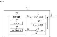
- FIG. 9 is a diagram schematically showing the configuration of the communication device according to the fourth embodiment.
- FIG. 10 is a timing chart schematically showing the count values of each signal and the addition / subtraction counter in the control circuit according to the fourth embodiment.
- FIG. 11 is a diagram schematically showing a specific configuration of the driver circuit according to the fifth embodiment.
- FIG. 12 is a diagram schematically showing a specific configuration of the control circuit according to the fifth embodiment.
- FIG. 13 is a diagram for explaining the operation of the communication device according to the fifth embodiment, and is a timing chart schematically showing a transmission signal, a bus waveform, and a gate voltage.
- FIG. 14 is a diagram for explaining an operation when the bus according to the sixth embodiment is stuck at a high level, and is a timing chart schematically showing a transmission signal, a bus waveform, a count value, and an operating state of a control circuit. Is.
- the communication system 1 shown in FIG. 1 is used, for example, for control communication between a plurality of electronic control devices mounted on a vehicle.
- the communication system 1 has a configuration in which a plurality of communication devices 2a, 2b, and 2c are connected via a bus 3 corresponding to a transmission line.
- the communication devices 2a, 2b, and 2c will be collectively referred to as the communication device 2 when it is not necessary to distinguish them from each other.
- the communication system 1 includes three communication devices 2, it may include two communication devices 2 or four or more communication devices 2.
- the plurality of communication devices 2 are configured as semiconductor integrated circuits, that is, ICs, and transmit and receive data via the bus 3.
- any one of the plurality of communication devices 2, specifically the communication device 2a is synchronized with the communication of the other communication devices 2b and 2c to perform transmission.
- the communication device 2a is also referred to as a master 2m
- the communication devices 2b and 2c are also referred to as a slave 2s.
- CXPI communication data transmission / reception is executed by CXPI communication.
- the master 2m supplies the clock to the slave 2s via the bus 3, and the slave 2s executes communication synchronized with the clock supplied via the bus 3.
- the bus 3 is configured so that when a high-level signal and a low-level signal are simultaneously output from different communication devices 2, the signal level on the bus 3 becomes low-level, and this function is used. Bus arbitration is realized. That is, in this case, the low level signal corresponds to the superior level which is the dominant signal level on the bus 3, and the high level signal corresponds to the inferior level which is the inferior signal level on the bus 3.
- a pulse width modulated signal that is, a PWM signal, in which the signal level changes from high level to low level at the boundary of bits and the signal level changes from low level to high level in the middle of the bits, is used as the transmission line code.
- the binary signal is represented by two types of PWM signals having different duty ratios.
- the one with a relatively short low-level period is referred to as a recessive code
- the one with a relatively long low-level period is referred to as a dominant code.
- the recessive code is set so that the first 1/3 period of 1 bit becomes the low level and the subsequent 2/3 period becomes the high level.
- the dominant code is set so that the first 2/3 period of 1 bit becomes the low level and the subsequent 1/3 period becomes the high level. For this reason, when the recessive code and the dominant code collide on the bus 3, the dominant code wins the arbitration.
- the master 2m and the slave 2s have substantially the same configuration, although some configurations such as the presence or absence of a configuration for supplying a clock are different. That is, as shown in FIG. 2, the communication device 2 includes a driver circuit 4, a receiver circuit 5, and a control circuit 6. A transmission signal TX output from the control circuit 6 is given to the driver circuit 4.
- the driver circuit 4 transmits data according to the transmission signal TX via the bus 3.
- the receiver circuit 5 receives the data transmitted via the bus 3 and outputs the received signal RX to the control circuit 6.
- the control circuit 6 is configured as a logic circuit, generates a transmission signal TX, and outputs the transmission signal TX to the driver circuit 4. Further, the control circuit 6 inputs the received signal RX output from the receiver circuit 5, and executes a predetermined process based on the input received signal RX.
- the receiver circuit 5 includes a filter circuit 7 and a comparator 8.
- the signal of the bus 3 is given to the non-inverting input terminal of the comparator 8 via the filter circuit 7.
- the filter circuit 7 is, for example, a low-pass filter, that is, an LPF or the like, and is inserted as a noise countermeasure.
- the output signal of the filter circuit 7 is a signal in which noise is removed and a delay corresponding to the time constant of the filter circuit 7 is generated with respect to the signal of the bus 3.
- a threshold signal Sa is given to the inverting input terminal of the comparator 8.
- the threshold signal Sa is a signal corresponding to the threshold Th for detecting an edge in which the signal level of the bus 3 changes from a high level to a low level.
- an edge is also referred to as a boundary edge.
- the comparator 8 outputs a high-level signal when the signal level of the bus 3 is higher than the threshold Th, and outputs a low-level signal when the signal level of the bus 3 is lower than the threshold Th. It is designed to do.
- the output signal of the comparator 8 is given to the control circuit 6 as the above-mentioned received signal RX.
- the receiver circuit 5 having the above configuration can detect an edge at which the signal level of the bus 3 changes from a high level to a low level, that is, a boundary edge. Specifically, the receiver circuit 5 can detect the boundary edge when the received signal RX, which is the output signal of the comparator 8, changes from the high level to the low level. As described above, in the present embodiment, the receiver circuit 5 has a function as an edge detection circuit.
- the driver circuit 4 has an open-drain output circuit configuration so as to enable the bus arbitration described above, and the transistors Q1, diodes D1, D2, and resistors R1 constituting the output stage thereof. And a drive circuit 9.
- the cathode of the diode D1 is connected to the bus 3.
- the anode of the diode D1 is connected to the power supply line L1 to which the power supply voltage Va is supplied via the pull-up resistor R1.
- the power supply voltage Va is a + B system power supply voltage generated from the power supply + B of the battery mounted on the vehicle.
- Transistor Q1 is an N-channel type MOS transistor, and its drain is connected to bus 3 via a diode D2 in the opposite direction.
- the source of the transistor Q1 is connected to the ground which is the reference potential (0V) of the circuit.
- the transistor Q1 functions as a switching element capable of setting the signal level of the bus 3 to a low level (0V) by turning it on.
- the drive circuit 9 drives the transistor Q1 based on the transmission signal TX given from the control circuit 6. In other words, the operation of the drive circuit 9 is controlled by the control circuit 6.
- the drive circuit 9 includes transistors Q2 to Q5, diodes D3, current sources 10 to 12, capacitors C1 and C2, resistors R2, and a gate driver 13.
- the transistor Q2 is an N-channel type MOS transistor, and a transmission signal TX is given to the gate thereof.
- the source of transistor Q2 is connected to ground and its drain is connected to node N1.
- the transistor Q3 is an N-channel type MOS transistor, and its source is connected to the ground via the diode D3 in the forward direction.
- the transistor Q3 is connected to a so-called diode, and its gate and drain are commonly connected and connected to the node N1.
- the current source 10 is connected between the power supply line L2 to which the power supply voltage Vb is supplied and the node N1.
- the power supply voltage Vb is a power supply voltage of a system different from the power supply voltage of the + B system such as a 5V power supply system.
- the power supply voltage Vb may be a + B system power supply voltage.
- the transistor Q4 is an NPN type bipolar transistor, and its base is connected to the node N1.
- the collector of the transistor Q4 is connected to the power line L2, and its emitter is connected to the node N2.
- the transistor Q5 is a P-channel type MOS transistor, and a transmission signal TX is given to the gate thereof.
- the source of the transistor Q5 is connected to the power supply line L2, and its drain is connected to the node N2 via the current source 11.
- the current source 12 is connected between the node N2 and the ground.
- the gate driver 13 functions as a mere buffer, its input terminal is connected to the node N2, and its output terminal is connected to the gate of the transistor Q1.
- the gate of the transistor Q1 corresponds to the control terminal of the switching element, and the gate voltage corresponds to the control voltage.
- the transmission signal TX output from the control circuit 6 is a binary signal, and is an off command that commands the off drive of the transistor Q1 at a high level and an on command that commands the on drive of the transistor Q1 at a low level. ..
- the high level of the transmission signal TX is a voltage value at which the transistor Q2 can be turned on and the transistor Q5 can be turned off, and is, for example, a voltage value equivalent to the power supply voltage Vb.
- the low level of the transmission signal TX is a voltage value at which the transistor Q2 can be turned off and the transistor Q5 can be turned on, and is, for example, 0 V.
- the master 2m In CXPI communication, the master 2m always outputs a recessive code, which is the clock described above.
- the slave 2s operates in synchronization with this clock. Specifically, the slave 2s operates in synchronization with the timing at which the boundary edge is detected by the receiver circuit 5 as described above, that is, the timing at which the falling edge of the clock is detected.
- the control circuit 6 gives a low-level transmission signal TX to the drive circuit 9 when the boundary edge is detected. Then, the drive circuit 9 drives the transistor Q1 on when a low-level transmission signal TX is given.
- the gate voltage of the transistor Q1 reaches the threshold voltage Vt (Q1) from the boundary edge, which is the timing when the signal level on the bus 3 changes from the high level to the low level, that is, the falling timing of the clock, and the transistor Q1
- a delay time which is the time it takes to turn on. This delay time is determined by the delay in the filter circuit 7, the delay in the comparator 8, the logic delay in the control circuit 6, the delay associated with the circuit operation of the driver circuit 4, and the like.
- Such a delay time needs to satisfy the time specified by the communication protocol of CXPI (for example, 0.11 Tbit). Note that 1 Tbit is the baud rate cycle of the bus.
- the communication device 2 of the present embodiment is provided with a delay shortening unit 14 for shortening such a delay time.
- the delay shortening unit 14 is composed of the transistors Q2, Q3, Q4, the diode D3, and the current source 10 of the drive circuit 9. That is, in the present embodiment, the delay shortening unit 14 is provided in the drive circuit 9.
- the transistor Q3 used has a threshold voltage Vt (Q3) lower than the threshold voltage Vt (Q1) at which the transistor Q1 turns on by a predetermined value ⁇ . That is, the relationship between the threshold voltage Vt (Q3) and the threshold voltage Vt (Q1) is expressed by the following equation (2).
- Vt (Q3) Vt (Q1) - ⁇ (2)
- the gate voltage of the transistor Q1 is set to a predetermined value ⁇ rather than the threshold voltage Vt (Q1) during the period including the start time of the on period in which the drive circuit 9 drives the transistor Q1 on.
- the delay time is shortened by controlling the voltage so that the threshold voltage Vt (Q3) rises to a lower threshold voltage.
- the threshold voltage Vt (Q3) corresponds to the first voltage V1.
- the gate voltage of the transistor Q1 rises to the threshold voltage Vt (Q3) due to the voltage control described above, and then is constant at the gate of the transistor Q1. It is designed to perform constant current control to supply the current of.
- the transmission signal TX in the master 2m is referred to as a transmission signal TXM
- the transmission signal TX in the slave 2s is referred to as a transmission signal TXS
- the gate voltage of the transistor Q1 is referred to as Vg
- the threshold voltage Vt of the transistor Q1 ( Q1) is called Vt.
- the low level is referred to as “L”
- the high level is referred to as “H” for the binary signal.
- the time point t1 when the transmission signal TXM changes from the high level to the low level is the falling edge of the clock, which corresponds to the boundary edge.
- the transmission signal TXS is at a high level.
- the drive circuit 9 drives the transistor Q1 off. The operation of each part during the off period in which the drive circuit 9 drives the transistor Q1 off is as follows.
- the transistor Q2 since the transmission signal TXS is at a high level, the transistor Q2 is turned on and the transistor Q5 is turned off. Since the transistor Q5 is turned off, the current of the current source 12 discharges the gate-source capacitance of the transistor Q1, so that the gate voltage Vg is lowered and the transistor Q1 is turned off. Therefore, the signal level of the bus 3 is maintained at a high level during the period before the time point t1. Further, since the transistor Q2 is turned on, the transistors Q3 and Q4 are turned off. Therefore, the delay shortening unit 14 has no effect on the voltage VN2 of the node N2 and thus the gate voltage Vg of the transistor Q1.
- the boundary edge is detected by the receiver circuit 5 at the time t2 when the signal level of the bus 3 decreases and reaches the threshold value Th after the transmission signal TXM changes to the low level at the time point t1.
- the time from the time point t1 to the time point t2 includes a delay related to the signal output on the master 2m side, a delay time due to the filter circuit 7 and the comparator 8.
- the control circuit 6 shifts the transmission signal TXS from the high level to the low level.
- the time from the time point t2 to the time point t3 when the transmission signal TXS turns to the low level includes a logic delay due to the control circuit 6.
- the transmission signal TXS becomes a low level.
- the drive circuit 9 drives the transistor Q1 on.
- the emitter voltage of the transistor Q4 that is, the voltage VN2 of the node N2 becomes the voltage represented by the following equation (4).
- the base-emitter voltage Vbe of the transistor Q4 is about the same as the forward voltage Vf of the diode D3.
- the gate voltage Vg of the transistor Q1 is the same voltage as the voltage VN2. Therefore, the gate voltage Vg of the transistor Q1 sharply rises from 0V to "Vt- ⁇ " at the time point t4 when a short time has passed from the time point t3.
- the time from the time point t3 to the time point t4 includes a delay time associated with the operation of each transistor.
- the gate voltage Vg of the transistor Q1 rises relatively gently with a constant slope from the time point t5 when a short time has passed from the time point t4.
- the slope of the increase in the gate voltage Vg at this time is determined by the current values I1 and I2 of the current sources 11 and 12 and the capacitance values of the capacitors C1 and C2. Then, at the time t6 when the gate voltage Vg of the transistor Q1 reaches the threshold voltage Vt, the transistor Q1 is turned on.
- the communication device 2 of the present embodiment includes a delay shortening unit 14 that shortens the delay time required from the boundary edge to the time when the transistor Q1 is turned on. According to such a configuration, the delay time can be shortened, and even in the case where the filter circuit 7 is inserted in front of the receiver circuit 5 as in the configuration of the present embodiment, the communication protocol is sufficient. Can be satisfied.
- the delay shortening unit 14 is provided in the drive circuit 9 of the driver circuit 4, and the gate voltage of the transistor Q1 is set during the period including the start time of the on period in which the drive circuit 9 drives the transistor Q1 on.
- the delay time is shortened by performing voltage control so as to rise to the first voltage V1 which is lower than the threshold voltage Vt by a predetermined value ⁇ .
- the effect of shortening the delay time according to the present embodiment will be described with reference to a comparative example corresponding to a conventional configuration in which the transistor Q1 is driven on by a constant current drive throughout the on period.
- the gate voltage of the transistor Q1 is relatively gentle with a constant slope from the vicinity of the time point t6 after the time point t4 when the gate voltage starts to rise in the present embodiment.
- the comparison is made until the gate voltage reaches the threshold voltage Vt and the transistor Q1 turns on. It will take a long time.
- the delay time due to the operation of the drive circuit 9 is the time from the time point t1 to the time point t7, which is longer than the time from the time point t1 to the time point t6 which is the delay time in the present embodiment.
- the gate voltage of the transistor Q1 rises relatively steeply to the first voltage V1 at once during the period including the start time of the on period.
- the constant current control is performed so that the gate voltage reaches the threshold voltage Vt and the transistor Q1 Turn on.
- the gate voltage of the transistor Q1 is raised to the first voltage V1 at a time, which is caused by the turn-on time of the transistor Q1, that is, the operation of the drive circuit 9. The delay time is reduced.
- the drive circuit 9 of the present embodiment is a constant current control that supplies a constant current to the gate of the transistor Q1 after the gate voltage of the transistor Q1 rises to the first voltage V1 by performing the voltage control as described above. I do.
- the gate voltage of the transistor Q1 rises to the first voltage V1 and then rises relatively gently with a constant slope to reach the threshold voltage Vt.
- the gate voltage rises sharply and reaches the threshold voltage Vt and the transistor Q1 is turned on, there is a concern that the emission may deteriorate due to the turning on operation.
- the gate voltage rises relatively slowly to reach the threshold voltage Vt, and the transistor Q1 is turned on. Therefore, according to the present embodiment, it is possible to reduce the risk of such deterioration of emissions while shortening the delay time caused by the operation of the drive circuit 9.
- the delay shortening unit 14 of the first embodiment is configured to indirectly control the gate voltage of the transistor Q1 by controlling the voltage of the node N2, that is, the input terminal of the gate driver 13.
- the delay shortening unit may have a configuration that directly controls the gate voltage of the transistor Q1.
- the driver circuit 21 of this embodiment has a configuration as shown in FIG. That is, the driver circuit 21 of the present embodiment is different from the driver circuit 4 of the first embodiment shown in FIG. 4 in that the drive circuit 22 is provided in place of the drive circuit 9.
- the drive circuit 22 has the same configuration as the drive circuit 9, but the connection destination of the emitter of the transistor Q4 is different.
- the emitter of the transistor Q4 is connected not to the node N2 but to the output terminal of the gate driver 13, that is, the gate of the transistor Q1.
- the delay shortening unit 23 is composed of the transistors Q2, Q3, Q4, the diode D3, and the current source 10 of the drive circuit 22. As described above, the delay shortening unit 23 of the present embodiment is configured to directly control the gate voltage of the transistor Q1.
- the gate voltage of the transistor Q1 is set to the threshold voltage Vt (Q1) during the period including the start time of the on period in which the drive circuit 22 drives the transistor Q1 on, as in the first embodiment. ), It is possible to control the voltage so that the voltage rises to the threshold voltage Vt (Q3), which is lower than the predetermined value ⁇ . Therefore, also in this embodiment, the delay time can be shortened as in the first embodiment.
- the driver circuit 31 of the present embodiment has a diode D21 added to the driver circuit 4 of the first embodiment shown in FIG. 4, and the drive circuit 32 is replaced with the drive circuit 9. It is different in that it has.
- the anode of the diode D21 is connected to the bus 3, and its cathode is connected to the anode of the diode D2. That is, in this case, the drain of the transistor Q1 is connected to the bus 3 via the two diodes D2 and D21 in opposite directions. It is assumed that such a diode D21 is provided only in the slave 2s and not in the master 2m. That is, in the master 2m, it is assumed that the drain of the transistor Q1 is connected to the bus 3 via one diode D2 in the opposite direction as in the driver circuit 4 of the first embodiment.
- the drive circuit 32 is different from the drive circuit 9 in that the switches S21, the filter circuit 33, and the diodes D22 and D23 are provided in place of the transistors Q2 to Q5, the current sources 10, 11 and the diode D3.
- the switch S21 opens and closes between the power supply line L2 and the node N2, and its on / off is controlled by the transmission signal TX bar which is an inverted signal of the transmission signal TX.
- the transmission signal TX bar is indicated by adding “-” above the TX.
- the switch S21 is turned on when the transmission signal TX bar is at a high level and is turned off when the transmission signal TX bar is at a low level.
- one terminal of the switch S21 is connected to the power supply line L2, and the other terminal is connected to the input terminal of the filter circuit 33.
- the filter circuit 33 is, for example, a CR filter composed of a resistor and a capacitor.
- the output terminal of the filter circuit 33 is connected to the node N2 via the diodes D22 and D23 in the forward direction.
- the switch S21 can be configured by using a semiconductor switching element such as a MOS transistor.
- the delay shortening unit 34 is composed of the switch S21, the filter circuit 33, and the diodes D22 and D23. That is, the delay shortening unit 34 is provided in the drive circuit 32.
- the power supply voltage Vb is a voltage sufficiently higher than the threshold voltage Vt of the transistor Q1.
- the drive circuit 32 provided with the delay shortening unit 34 performs voltage control so that the gate voltage of the transistor Q1 rises to a second voltage V2 higher than the threshold voltage Vt.
- the delay shortening unit 34 includes a filter circuit 33 interposed in series with the supply path of the second voltage V2 to the gate of the transistor Q1.
- the operation of each part during the off period in which the drive circuit 32 drives the transistor Q1 off is as follows. That is, since the transmission signal TXS is at a high level, the switch S21 is turned off. As a result, the gate-source capacitance of the transistor Q1 is discharged by the current of the current source 12, so that the gate voltage Vg drops and the transistor Q1 is turned off.
- each part during the ON period in which the drive circuit 32 drives the transistor Q1 on is as follows. That is, since the transmission signal TXS is at a low level, the switch S21 is turned on. Since the switch S21 is on, the second voltage V2 is supplied to the node N2 and eventually to the gate of the transistor Q1.
- the voltage VN2 of the node N2, and thus the gate voltage Vg of the transistor Q1 has a relatively steep slope from the time t31 when a short time has passed from the time t3 when the transmission signal TXS turns to the low level, and the voltage from 0V to the second voltage. It rises toward V2.
- the filter circuit 33 is interposed in series in the supply path of the second voltage V2 with respect to the gate of the transistor Q1. Therefore, the waveform of the gate voltage Vg of the transistor Q1 becomes a slightly dull waveform due to the action of the filter circuit 33. Then, at the time t32 when the gate voltage Vg of the transistor Q1 reaches the threshold voltage Vt, the transistor Q1 is turned on.
- the present embodiment described above also includes the delay shortening unit 34 that shortens the delay time required from the boundary edge to the time when the transistor Q1 is turned on, the same effect as that of the first embodiment can be obtained. Further, in this case, the delay shortening unit 34 performs voltage control so that the gate voltage of the transistor Q1 rises to a second voltage V2 higher than the threshold voltage Vt throughout the on period of driving the transistor Q1 on. .. Therefore, according to the present embodiment, the delay time due to the operation of the drive circuit 32 can be shortened as compared with the first embodiment as well as the comparative example.
- the slope of the increase in the gate voltage when reaching the threshold voltage Vt becomes steeper than in the configuration of the first embodiment, so there is a concern that the emission may deteriorate.
- the waveform of the gate voltage of the transistor Q1 is slightly dull due to the action of the filter circuit 33 interposed in the supply path of the second voltage V2 with respect to the gate of the transistor Q1. Therefore, in the present embodiment, the slope of the increase in the gate voltage when reaching the threshold voltage Vt becomes slightly gentle, and the risk of deterioration of emissions is reduced.
- the gate voltage of the transistor Q1 in the output stage rises relatively steeply, and the transistor Q1 turns on relatively steeply. Therefore, there is a possibility that a current is drawn from the master 2m to the slave 2s through the bus 3. Specifically, a current may be drawn from the power supply line L1 to which the power supply voltage Va of the master 2 m is supplied to the slave 2s via the resistor R1, the diode D1 and the bus 3. Such a current leads to deterioration of emissions.
- the drain of the transistor Q1 in the output stage is connected to the bus 3 via the two diodes D2 and D21 in opposite directions. ing.
- the drain of the transistor Q1 in the output stage is connected to the bus 3 via one diode D2 in the opposite direction. Therefore, the output terminal of the slave 2s has a higher voltage than the output terminal of the master 2m by the forward voltage Vf of the diode D21.
- the transistor Q1 of the driver circuit 31 of the slave 2s is suddenly turned on, the current from the power supply line L1 of the master 2m does not flow to the slave 2s side and passes through the transistor Q1 of the output stage of the master 2m. Flows to the ground.
- the possibility that the current is drawn from the master 2m to the slave 2s is suppressed to a low level, so that the risk of deterioration of emissions due to this is reduced.
- the gate voltage of the transistor Q1 rises relatively slowly and the transistor Q1 turns on relatively slowly as compared with the configuration of the present embodiment. Therefore, from the master 2m. It is unlikely that current will be drawn into the slave 2s.
- the configuration of the first embodiment as in the configuration of the present embodiment, if the drain of the transistor Q1 is connected to the bus 3 via the two diodes D2 and D21 in opposite directions, the master 2m to the slave The possibility that the current is drawn into the 2s can be further reduced, and the risk of deterioration of emissions due to this can be further reduced.
- the communication device 41 of the present embodiment includes a receiver circuit 42 instead of the receiver circuit 5 with respect to the communication device 2 of the first embodiment, and a control circuit instead of the control circuit 6. It is different in that it has 43.
- the receiver circuit 42 is different from the receiver circuit 5 shown in FIG. 3 in that the filter circuit 7 is omitted. In this case, the signal of the bus 3 is directly given to the non-inverting input terminal of the comparator 8.
- the control circuit 43 has functions as a determination unit 44 and a noise detection unit 45.
- the determination unit 44 determines the code transmitted via the bus 3 by sampling the signal of the bus 3 at a predetermined sampling timing.
- the noise detection unit 45 detects the signal level of the bus 3 and detects the noise superimposed on the bus 3 based on the detection result. Specifically, each of these functions is realized as follows.
- the control circuit 43 includes a digital filter circuit including an addition / subtraction counter that adds or subtracts based on the level of the received signal RX which is the output signal of the comparator 8.
- the addition / subtraction counter adds when the signal RX1 obtained by passing the received signal RX through the double matching filter included in the digital filter circuit is at a high level, and subtracts when the signal RX1 is at a low level. I do.
- the count value ct of the addition / subtraction counter is added when the signal RX1 is at a high level and is subtracted when the signal RX1 is at a low level.
- the signal RX2 corresponding to the received signal RX is generated based on the count value ct of such an addition / subtraction counter.
- the signal RX2 is a signal that turns to a low level when the count value ct reaches the lower limit value and turns to a high level when the count value ct reaches the upper limit value.
- the determination unit 44 determines the code transmitted via the bus 3 by sampling the signal RX2 generated in this way at a predetermined sampling timing.
- the sampling timing this time is determined according to the time obtained by adding a predetermined specified time corresponding to 6% of the bit rate to the previous Lo width.
- the sampling timing of this time is the time when the time obtained by adding the specified time to the previous Lo width elapses from the time of falling of the signal RX2 this time.
- addition / subtraction counter when noise is not superimposed on the bus 3, once subtraction is started, subtraction is continuously performed for a predetermined period thereafter, and once addition is started, after that. The addition is continuously performed for the predetermined period of.
- chattering occurs in the output of the comparator 8 due to noise superimposed on the bus 3 and the level of the received signal RX fluctuates, the addition / subtraction counter repeats addition and subtraction.
- the noise detection unit 45 determines that noise is superimposed on the bus 3 when the addition and subtraction by the addition / subtraction counter are repeatedly performed. Further, the noise detection unit 45 determines that the periods TNf and TNr in which the count value ct of the addition / subtraction counter increases / decreases are the noise detection periods in which the noise is detected.
- the Lo width described above accurately represents the low period at which the signal of the bus 3 is at the low level in the normal state where noise is not superimposed on the bus 3, but when noise is superimposed on the bus 3, it becomes the actual low period. Can be different. Specifically, when the received signal RX corresponding to the vicinity of the falling edge of the signal of the bus 3 fluctuates due to the influence of noise, the time until the count value ct reaches the lower limit value is delayed, and as a result, the signal RX2 Lo width becomes shorter than the actual row period.
- the received signal RX corresponding to the vicinity of the rising edge of the signal of the bus 3 fluctuates due to the influence of noise, the time until the count value ct reaches the upper limit value is delayed, and as a result, the Lo width of the signal RX2 becomes large. It will be longer than the actual row period.
- the sampling timing this time is determined based on the previous Lo width shorter than the actual row period, but the Lo width this time accurately represents the actual row period. Therefore, in the first case, the sampling timing this time is a timing that is ahead of the original timing, and as a result, it is erroneously determined that the signal of the bus 3 is at a low level even though it is at a high level. There is a risk.
- the sampling timing this time is determined based on the previous Lo width that accurately represents the actual row period, but the Lo width this time is longer than the actual row period. Therefore, even though the signal of the bus 3 is high level, it may be erroneously determined to be low level.
- the determination unit 44 delays the sampling timing by a predetermined time according to the period in which the noise is detected.
- the predetermined time is a period in which the above-mentioned period TNf and the period TNr are added.
- the delay time required from the boundary edge to the time when the transistor Q1 is turned on is shortened as compared with the configuration of the first embodiment. There is a merit that it is done.
- the filter circuit 7 for removing noise is not provided, there is a demerit that the possibility of erroneous determination due to the influence of noise increases.
- the present embodiment since the occurrence of erroneous determination due to the influence of noise is prevented as described above, there is no demerit due to the absence of the filter circuit 7, and only the merit is enjoyed. be able to.
- FIGS. 11 to 13 a fifth embodiment in which the specific configurations of the driver circuit and the control circuit have been changed with respect to the first embodiment will be described with reference to FIGS. 11 to 13.
- the driver circuit 51 of the present embodiment is different from the driver circuit 4 of the first embodiment shown in FIG. 4 in that the drive circuit 52 is provided in place of the drive circuit 9. There is.
- the drive circuit 52 is different from the drive circuit 9 in that the delay shortening unit 14 is omitted and that the switch S51 is provided instead of the transistor Q5.
- One terminal of the switch S51 is connected to the power supply line L2, and the other terminal is connected to the node N2 via the current source 11.
- the on / off of the switch S51 is controlled by the transmission signal TX.
- the switch S51 is turned off when the transmission signal TX is at a high level and is turned on when the transmission signal TX is at a low level.
- the switch S51 can be configured by using a semiconductor switching element such as a MOS transistor.
- the current source 12 is configured so that its operation can be stopped. Specifically, the current source 12 stops the operation during the period when the cut signal PSCM, which will be described later, is at a high level, and executes the operation during the period when the cut signal PSCM is at a low level.
- the control circuit 53 of the present embodiment has functions as a learning control unit 54, a predictive control unit 55, and a first-out control unit 56.
- the learning control unit 54 executes learning control for learning the period of the boundary edge based on the detection result of the boundary edge by the receiver circuit 5 functioning as the edge detection circuit.
- the learning control unit 54 includes a counter 54a, which is a hardware timer counter that measures a 1-bit rate.
- the counter 54a executes the counting operation from the time when the boundary edge is detected to the time when the boundary edge is detected next.
- the counter 54a starts the counting operation when the boundary edge is detected, and thereafter restarts the counting operation after clearing the count value at each time when the boundary edge is detected.
- the learning control unit 54 learns the period of the boundary edge based on the count value of the counter 54a. That is, the learning control unit 54 learns the count value when the counter 54a is cleared as the learning value of the boundary edge cycle each time. Since the bit rate is constant, such a learning value shows a constant value. For example, when the bit rate is 20 kbps and the counter 54a operates with a system clock of 4.5 MHz, the learning value is constant at "225".
- the prediction control unit 55 executes predictive control that predicts the timing at which the next boundary edge is detected based on the cycle of the boundary edge learned by the learning control unit 54 executing the learning control. Specifically, the prediction control unit 55 can predict the timing at which the next boundary edge is detected based on the learning value learned by the learning control and the current count value of the counter 54a.
- the first-out control unit 56 executes first-out control that gives an on-command to the drive circuit 52, that is, a low-level transmission signal TX at a time point earlier than the timing predicted by the prediction control unit 55 executing the prediction control. .. Specifically, the advance control unit 56 starts outputting the low-level transmission signal TX at a time point that is a predetermined number of clocks before the time point when the count value of the counter 54a matches the learning value.
- the advance control unit 56 starts outputting the low-level transmission signal TX when the count value of the counter 54a is "220" and the counter matches. ing.
- the setting of the predetermined number of clocks that is, the setting of how much before the predicted timing to start the output, can be appropriately changed and adjusted according to various specifications and the like.
- the delay time required from the boundary edge to the time when the transistor Q1 is turned on is shortened by executing each of the above-mentioned controls by the learning control unit 54, the predictive control unit 55, and the advance control unit 56. .. That is, in this case, the delay shortening unit 57 is configured by the learning control unit 54, the prediction control unit 55, and the advance control unit 56. As described above, in the present embodiment, the delay shortening unit 57 is provided in the control circuit 53.
- the control circuit 53 generates the cut signal PSCM described above.
- the cut signal PSCM is high in the first-out period, which is the period from the time when the output of the low-level transmission signal TX is started by executing the first-out control to the timing when the next boundary edge predicted by the prediction control is detected. It becomes a level and becomes a low level in other periods.
- the operation of each part during the off period in which the drive circuit 52 drives the transistor Q1 off is as follows. That is, since the transmission signal TXS is at a high level, the switch S51 is turned off. As a result, the gate-source capacitance of the transistor Q1 is discharged by the current of the current source 12, so that the gate voltage Vg drops and the transistor Q1 is turned off.
- the control circuit 53 executes each of the above-mentioned controls, so that the transmission signal is transmitted at a time point t51 before the time point t3 when the control circuit 6 of the first embodiment shifts the transmission signal TXS from the high level to the low level. Turn TXS from high level to low level. During the period after the time point t51, the transmission signal TXS becomes a low level. During such a period, the drive circuit 52 drives the transistor Q1 on. The operation of each part during the ON period in which the drive circuit 52 drives the transistor Q1 on is as follows.
- the switch S51 since the transmission signal TXS is at a low level, the switch S51 is turned on. Further, the cut signal PSCM becomes a high level during the advance period from the time point t51 to the time point t3. Therefore, during the first-out period, the output current of the current source 11 branches and flows so as to charge each of the capacitors C1 and C2. After that, when the cut signal PSCM turns to a low level at the time point t3, a current having a current value I2 corresponding to the difference between the output current of the current source 11 and the output current of the current source 12 is supplied toward the gate of the transistor Q1. It will be.
- the gate voltage Vg of the transistor Q1 rises relatively gently with a constant slope from the time point t52 when a short time has passed from the time point t51.
- the slope of the increase in the gate voltage Vg at this time is determined by the current values I1 and I2 of the current sources 11 and 12 and the capacitance values of the capacitors C1 and C2. Then, at the time t53 when the gate voltage Vg of the transistor Q1 reaches the threshold voltage Vt, the transistor Q1 is turned on.
- the present embodiment described above also includes the delay shortening unit 57 that shortens the delay time required from the boundary edge to the time when the transistor Q1 is turned on, the same effect as that of the first embodiment can be obtained.
- the delay shortening unit 57 provided in the control circuit 53 executes various controls to switch the transmission signal TX to the low level at a timing ahead of the comparative example corresponding to the conventional configuration. .. Therefore, according to the present embodiment, by setting the timing for advancing the transmission signal TX, not only the delay time due to the operation of the drive circuit 52, but also the logic delay in the control circuit 53, the delay in the filter circuit 7, and the comparator 8 It is possible to significantly reduce the overall delay time including the delay in.
- the drive circuit 52 of the present embodiment has a configuration in which the transistor Q1 is driven on by constant current drive throughout the on period, as in the comparative example described in the first embodiment. Therefore, in the present embodiment, the gate voltage rises relatively slowly to reach the threshold voltage Vt, and the transistor Q1 is turned on. Therefore, according to the present embodiment, it is possible to reduce the risk of deterioration of emissions due to the ON operation of the transistor Q1.
- the control circuit 53 does not start the output of the low-level transmission signal TXS triggered by the change of the signal of the bus 3, but is based on the learned value of the learned boundary edge period.
- the output of the low-level transmission signal TXS is started ahead of schedule, and there is no need to wait for a change in the signal of the bus 3. That is, the control circuit 53 starts to output the low-level transmission signal TXS when the dominant code is output even if the clock is not output from the master 2m.
- the control circuit 53 outputs the low level transmission signal TXS based on the learning value. That is, there is a possibility that the signal level of the bus 3 is changed and the behavior is as if the clock from the master 2 m is supplied. Therefore, in the configuration of the fifth embodiment, even if the bus 3 is fixed at a high level, the slave 2s may run by itself when continuously outputting the dominant code. In the following, the sticking of the bus 3 to a high level is referred to as Hi sticking.
- the UART frame is decoded and a signal is put on the bus 3.
- the UART always contains at least one stop bit. Therefore, in the operation of the slave 2s, the timing of outputting the recessive code corresponding to "logical value: 1" to the bus 3 is always included.
- the control circuit 53 When the slave 2s outputs the recessive code corresponding to the stop bit when the bus 3 is fixed to Hi, the boundary edge is not detected for a relatively long period of time. Therefore, the count value of the counter 54a is assumed as the period of the boundary edge. It is a very large value compared to the value (for example) "225"). Therefore, when the count value of the counter 54a reaches an upper limit value (for example, “1024”) larger than the value assumed as the period of the boundary edge, the control circuit 53 once resets the learning result by the learning control to perform the learning control. It is supposed to be executed again.
- the control circuit 53 stops the execution of the predictive control and the first-out control until the learning result by the learning control is obtained.
- the control circuit 53 includes a remeasurement counter that counts the number of times that the learning value is correctly obtained, and the period until the count value of the remeasurement counter becomes "3", that is, the learning value is The execution of the predictive control and the first-out control is stopped until three times are obtained.
- the count value of the counter 54a is cnt1
- the count value of the remeasurement counter is cnt2.
- the slave 2s In the period Ta, the slave 2s is in a state of continuously outputting the dominant code. Therefore, the slave 2s outputs the low-level transmission signal TXS based on the learning value even though the clock supply is stopped from the master 2m, that is, the signal level of the bus 3 is changed.
- the count value ct1 is "230", "235”, etc., and the cycle of the boundary edge. The value does not deviate significantly from the value assumed as.
- the slave 2s In the period Tb, the slave 2s is in a state of outputting a recessive code corresponding to, for example, a stop bit. Therefore, the count value ct1 of the counter 54a rises beyond the value assumed as the period of the boundary edge, and reaches the upper limit value “1024”. As a result, the control circuit 53 once resets the learning result of the learning control, executes the learning control again, and stops the execution of the predictive control and the first-out control. In FIG. 14, such an operating state is represented as a reset operation (during remeasurement). At this time, the count value of the remeasurement counter is cleared to "0".
- the clock supply is restarted from the master 2m.
- the learning value starts to be normally obtained by the learning control, and when the learning value is obtained three times, the control circuit 53 resumes the execution of the prediction control and the advance control.
- the slave 2s is in a normal operating state in which the slave 2s operates in synchronization with the clock from the master 2m. In FIG. 14, such an operating state is represented as a reset release operation.
- the control circuit 53 will perform the control circuit 53 when the count value of the counter 54a reaches the upper limit. Since it is determined that the bus 3 is fixed to Hi and the execution of the predictive control and the advance control is stopped, there is no possibility that the slave 2s will continue to operate without synchronizing with the clock supplied from the master 2m. Further, in this case, when the control circuit 53 determines that the bus 3 is fixed to Hi, the learning value is reset and the learning control is restarted, and when the learned value is correctly obtained by the restarted learning control, the prediction control and The first-out control is restarted. Therefore, when the abnormality on the master 2m side is resolved, the slave 2s can promptly resume the prediction control and the first-out control, and can return to the normal operation.
- the present disclosure is not limited to the communication devices 2 and 41 that perform CXPI communication exemplified in each of the above embodiments, and is synchronized with the communication of any one of a plurality of communication devices that transmit and receive data via a transmission line. It can be applied to all communication devices used in communication systems in which other communication devices transmit.
- the switching element provided in the output stage of the driver circuit 4 or the like is not limited to a MOS transistor such as the transistor Q1, and various semiconductor switching elements such as a bipolar transistor and a GaAs-MESFET can be used.
Landscapes
- Engineering & Computer Science (AREA)
- Computer Networks & Wireless Communication (AREA)
- Signal Processing (AREA)
- Physics & Mathematics (AREA)
- Nonlinear Science (AREA)
- Computer Hardware Design (AREA)
- Power Engineering (AREA)
- Computing Systems (AREA)
- General Engineering & Computer Science (AREA)
- Mathematical Physics (AREA)
- Logic Circuits (AREA)
- Dc Digital Transmission (AREA)
Priority Applications (1)
| Application Number | Priority Date | Filing Date | Title |
|---|---|---|---|
| US17/667,730 US12212647B2 (en) | 2019-08-30 | 2022-02-09 | Communication apparatus |
Applications Claiming Priority (2)
| Application Number | Priority Date | Filing Date | Title |
|---|---|---|---|
| JP2019-158359 | 2019-08-30 | ||
| JP2019158359A JP7251412B2 (ja) | 2019-08-30 | 2019-08-30 | 通信装置 |
Related Child Applications (1)
| Application Number | Title | Priority Date | Filing Date |
|---|---|---|---|
| US17/667,730 Continuation US12212647B2 (en) | 2019-08-30 | 2022-02-09 | Communication apparatus |
Publications (1)
| Publication Number | Publication Date |
|---|---|
| WO2021039709A1 true WO2021039709A1 (ja) | 2021-03-04 |
Family
ID=74684170
Family Applications (1)
| Application Number | Title | Priority Date | Filing Date |
|---|---|---|---|
| PCT/JP2020/031820 Ceased WO2021039709A1 (ja) | 2019-08-30 | 2020-08-24 | 通信装置 |
Country Status (3)
| Country | Link |
|---|---|
| US (1) | US12212647B2 (enExample) |
| JP (1) | JP7251412B2 (enExample) |
| WO (1) | WO2021039709A1 (enExample) |
Families Citing this family (4)
| Publication number | Priority date | Publication date | Assignee | Title |
|---|---|---|---|---|
| KR102559669B1 (ko) * | 2021-12-01 | 2023-07-27 | 한국생산기술연구원 | 자율주행 차량의 원격제어 안전성 확보를 위한 양방향 재귀 필터 시스템 및 이의 제어방법 |
| JP7677170B2 (ja) * | 2022-01-28 | 2025-05-15 | 株式会社デンソー | 通信装置 |
| JP7731835B6 (ja) | 2022-03-18 | 2025-09-19 | 株式会社東芝 | 通信システム、送信装置及び受信装置 |
| JP7739214B2 (ja) | 2022-03-23 | 2025-09-16 | 株式会社東芝 | 送信装置、受信装置、送信方法及び受信方法 |
Citations (3)
| Publication number | Priority date | Publication date | Assignee | Title |
|---|---|---|---|---|
| JP2004241930A (ja) * | 2003-02-04 | 2004-08-26 | Fujitsu Ltd | 出力回路 |
| JP2017041693A (ja) * | 2015-08-18 | 2017-02-23 | 株式会社デンソー | 通信装置及び通信システム |
| JP2018007237A (ja) * | 2016-03-14 | 2018-01-11 | サイプレス セミコンダクター コーポレーション | 通信用送受信機及び通信制御方法 |
Family Cites Families (47)
| Publication number | Priority date | Publication date | Assignee | Title |
|---|---|---|---|---|
| US6977492B2 (en) * | 2002-07-10 | 2005-12-20 | Marvell World Trade Ltd. | Output regulator |
| US7375593B2 (en) * | 2005-01-19 | 2008-05-20 | Paul William Ronald Self | Circuits and methods of generating and controlling signals on an integrated circuit |
| US8169185B2 (en) * | 2006-01-31 | 2012-05-01 | Mojo Mobility, Inc. | System and method for inductive charging of portable devices |
| WO2008076406A2 (en) * | 2006-12-14 | 2008-06-26 | Ion Torrent Systems Incorporated | Methods and apparatus for measuring analytes using large scale fet arrays |
| WO2008155917A1 (ja) * | 2007-06-19 | 2008-12-24 | Panasonic Corporation | スイッチング素子駆動回路 |
| GB2469637A (en) * | 2009-04-20 | 2010-10-27 | Advanced Risc Mach Ltd | A CMOS voltage-level-reducing input circuit with hysteresis |
| CN102845037B (zh) * | 2009-11-05 | 2016-03-16 | 罗姆股份有限公司 | 信号传输电路器件、半导体器件、检查半导体器件的方法和装置、信号传输器件以及使用信号传输器件的电机驱动装置 |
| JP2012065235A (ja) * | 2010-09-17 | 2012-03-29 | Toshiba Corp | 電圧出力回路 |
| US20130076424A1 (en) * | 2011-09-23 | 2013-03-28 | Qualcomm Incorporated | System and method for reducing cross coupling effects |
| JP5825144B2 (ja) * | 2012-02-28 | 2015-12-02 | 富士電機株式会社 | 半導体装置およびハイサイド回路の駆動方法 |
| JP5609930B2 (ja) | 2012-07-31 | 2014-10-22 | 株式会社デンソー | トランシーバ |
| US9257908B2 (en) * | 2013-03-15 | 2016-02-09 | Maxim Integrated Products, Inc. | Systems and methods to auto-adjust zero cross circuits for switching regulators |
| WO2015045534A1 (ja) * | 2013-09-27 | 2015-04-02 | 富士電機株式会社 | 駆動回路および半導体装置 |
| DE112013007602T5 (de) * | 2013-11-14 | 2016-08-18 | Mitsubishi Electric Corporation | Halbleiterelement-Treiberschaltung |
| EP2911324B1 (en) * | 2014-02-24 | 2019-05-15 | Sony Corporation | Method and controller for collision avoidance |
| KR20160009429A (ko) * | 2014-07-16 | 2016-01-26 | 삼성전자주식회사 | Pvt 변동에 둔감한 딜레이 컨트롤 시스템 및 그 제어 방법 |
| US9647476B2 (en) * | 2014-09-16 | 2017-05-09 | Navitas Semiconductor Inc. | Integrated bias supply, reference and bias current circuits for GaN devices |
| JP2017534237A (ja) * | 2014-11-11 | 2017-11-16 | マシイネンフアブリーク・ラインハウゼン・ゲゼルシヤフト・ミツト・ベシユレンクテル・ハフツング | 抵抗器エミュレーション及びゲートブースト |
| US9808246B2 (en) * | 2015-03-06 | 2017-11-07 | Ethicon Endo-Surgery, Llc | Method of operating a powered surgical instrument |
| CN107005234B (zh) * | 2015-06-16 | 2020-09-22 | 富士电机株式会社 | 半导体装置 |
| WO2017038592A1 (ja) * | 2015-09-01 | 2017-03-09 | 株式会社デンソー | リンギング抑制回路 |
| JP2017158011A (ja) * | 2016-03-01 | 2017-09-07 | 株式会社デンソー | 信号出力回路 |
| US10128803B2 (en) * | 2016-04-22 | 2018-11-13 | Cirrus Logic, Inc. | Systems and methods for predictive switching in audio amplifiers |
| JP2017224926A (ja) * | 2016-06-14 | 2017-12-21 | 株式会社デンソー | チャタリング除去回路 |
| US20180331682A1 (en) * | 2016-06-22 | 2018-11-15 | Sarda Technologies, Inc. | Gate Driver for Depletion-Mode Transistors |
| CN116101187A (zh) * | 2016-06-24 | 2023-05-12 | 矢崎总业株式会社 | 车辆电路体 |
| US10411922B2 (en) * | 2016-09-16 | 2019-09-10 | Kandou Labs, S.A. | Data-driven phase detector element for phase locked loops |
| JP6542174B2 (ja) * | 2016-09-21 | 2019-07-10 | 株式会社東芝 | 半導体装置及び半導体装置の制御方法 |
| JP6939059B2 (ja) * | 2017-04-27 | 2021-09-22 | 富士電機株式会社 | 半導体素子の駆動装置 |
| DE112018002643T5 (de) * | 2017-05-22 | 2020-05-07 | Invention Mine, Llc | Multimodale datengetriebene taktwiederherstellungsschaltung |
| US10116297B1 (en) * | 2017-06-19 | 2018-10-30 | Psemi Corporation | DC-coupled high-voltage level shifter |
| US10348293B2 (en) * | 2017-06-19 | 2019-07-09 | Psemi Corporation | Timing controller for dead-time control |
| JP6956797B2 (ja) * | 2017-10-24 | 2021-11-02 | 三菱電機株式会社 | 判定装置、判定システム及び判定方法 |
| US11101673B2 (en) * | 2018-03-13 | 2021-08-24 | Cypress Semiconductor Corporation | Programmable gate driver control in USB power delivery |
| US10425073B1 (en) * | 2018-03-23 | 2019-09-24 | Dialog Semiconductor B.V. | Digital active diode circuit |
| JP7095388B2 (ja) * | 2018-05-11 | 2022-07-05 | 富士電機株式会社 | トーテムポール回路用駆動装置 |
| JP2019213349A (ja) * | 2018-06-05 | 2019-12-12 | 株式会社デンソー | 車両用照明制御システム |
| US10483977B1 (en) * | 2018-06-08 | 2019-11-19 | Texas Instruments Incorporated | Level shifter |
| JP2020017842A (ja) * | 2018-07-25 | 2020-01-30 | 株式会社東芝 | 非同期通信装置 |
| US10826374B2 (en) * | 2018-08-08 | 2020-11-03 | Semiconductor Components Industries, Llc | Control of pulse generator in driving control device |
| US10734892B2 (en) * | 2018-09-27 | 2020-08-04 | Psemi Corporation | Level shifter for power applications |
| JP7111970B2 (ja) * | 2018-12-20 | 2022-08-03 | 富士通株式会社 | 制御回路、制御方法及び制御プログラム |
| US10862399B1 (en) * | 2019-06-27 | 2020-12-08 | Cypress Semiconductor Corporation | Primary controller calibration and trimming using secondary controller in secondary-controlled flyback converters |
| US10951107B2 (en) * | 2019-06-27 | 2021-03-16 | Cypress Semiconductor Corporation | Communicating fault indications between primary and secondary controllers in a secondary-controlled flyback converter |
| CN110350902B (zh) * | 2019-07-18 | 2023-01-17 | 重庆惠科金扬科技有限公司 | 一种防误操作电路及防误操作装置 |
| US11114945B2 (en) * | 2019-08-22 | 2021-09-07 | Cypress Semiconductor Corporation | Secondary-controlled active clamp implementation for improved efficiency |
| CN117914323A (zh) * | 2024-01-19 | 2024-04-19 | 全阵光敏(北京)信息技术有限公司 | 一种模数转换电路、cmos-tdi图像传感器电路及其工作方法 |
-
2019
- 2019-08-30 JP JP2019158359A patent/JP7251412B2/ja active Active
-
2020
- 2020-08-24 WO PCT/JP2020/031820 patent/WO2021039709A1/ja not_active Ceased
-
2022
- 2022-02-09 US US17/667,730 patent/US12212647B2/en active Active
Patent Citations (3)
| Publication number | Priority date | Publication date | Assignee | Title |
|---|---|---|---|---|
| JP2004241930A (ja) * | 2003-02-04 | 2004-08-26 | Fujitsu Ltd | 出力回路 |
| JP2017041693A (ja) * | 2015-08-18 | 2017-02-23 | 株式会社デンソー | 通信装置及び通信システム |
| JP2018007237A (ja) * | 2016-03-14 | 2018-01-11 | サイプレス セミコンダクター コーポレーション | 通信用送受信機及び通信制御方法 |
Non-Patent Citations (1)
| Title |
|---|
| "CXPI BD 41000 FJ-C", ROHM SEMI CONDUCTOR, September 2015 (2015-09-01), XP055797153, Retrieved from the Internet <URL:https://www.rohm.co.jp/documents/11401/3280383/58F6937J_CXPI-transceiver_ss_J.pdf> [retrieved on 20201106] * |
Also Published As
| Publication number | Publication date |
|---|---|
| JP2021040171A (ja) | 2021-03-11 |
| US12212647B2 (en) | 2025-01-28 |
| US20220239460A1 (en) | 2022-07-28 |
| JP7251412B2 (ja) | 2023-04-04 |
Similar Documents
| Publication | Publication Date | Title |
|---|---|---|
| US12212647B2 (en) | Communication apparatus | |
| US9722610B2 (en) | Semiconductor device and high side circuit drive method | |
| US8405422B2 (en) | Level shift circuit | |
| CN104094525B (zh) | 半导体装置 | |
| CN105103447A (zh) | 驱动电路以及半导体装置 | |
| CN108322211B (zh) | 一种i/o接口电路输出状态的检测电路和电子系统 | |
| US8698543B1 (en) | Interface to a serial communications bus | |
| US9270505B2 (en) | Communication system | |
| US9543942B2 (en) | Method and apparatus for controlling an IGBT device | |
| KR100908550B1 (ko) | 파워 온 리셋 회로 | |
| CN107078733A (zh) | 驱动电路 | |
| US7064603B2 (en) | Driving circuit and semiconductor device | |
| JP5203791B2 (ja) | レベルシフト回路 | |
| US9852099B2 (en) | Slave communication device and bus communication system | |
| JP2009278406A (ja) | 半導体回路 | |
| US20110133562A1 (en) | Level shifter | |
| JP7677170B2 (ja) | 通信装置 | |
| US8487649B2 (en) | Output circuit, system including output circuit, and method of controlling output circuit | |
| US7804339B2 (en) | Serial bus interface circuit | |
| JP5360261B2 (ja) | 半導体回路 | |
| US20250047532A1 (en) | Communication device | |
| US7446565B2 (en) | Apparatus and method that provides active pull-up and logic translation from one signal mode to another signal mode | |
| JP2025113907A (ja) | 半導体集積回路 | |
| CN114696806A (zh) | 用于实现射频开关快速切换的电路 | |
| JP2008283292A (ja) | 半導体装置 |
Legal Events
| Date | Code | Title | Description |
|---|---|---|---|
| 121 | Ep: the epo has been informed by wipo that ep was designated in this application |
Ref document number: 20858543 Country of ref document: EP Kind code of ref document: A1 |
|
| NENP | Non-entry into the national phase |
Ref country code: DE |
|
| 122 | Ep: pct application non-entry in european phase |
Ref document number: 20858543 Country of ref document: EP Kind code of ref document: A1 |