WO2021039709A1 - 通信装置 - Google Patents
通信装置 Download PDFInfo
- Publication number
- WO2021039709A1 WO2021039709A1 PCT/JP2020/031820 JP2020031820W WO2021039709A1 WO 2021039709 A1 WO2021039709 A1 WO 2021039709A1 JP 2020031820 W JP2020031820 W JP 2020031820W WO 2021039709 A1 WO2021039709 A1 WO 2021039709A1
- Authority
- WO
- WIPO (PCT)
- Prior art keywords
- voltage
- control
- circuit
- transistor
- edge
- Prior art date
Links
Images


Classifications
-
- H—ELECTRICITY
- H04—ELECTRIC COMMUNICATION TECHNIQUE
- H04L—TRANSMISSION OF DIGITAL INFORMATION, e.g. TELEGRAPHIC COMMUNICATION
- H04L7/00—Arrangements for synchronising receiver with transmitter
- H04L7/0016—Arrangements for synchronising receiver with transmitter correction of synchronization errors
- H04L7/0033—Correction by delay
-
- H—ELECTRICITY
- H03—ELECTRONIC CIRCUITRY
- H03K—PULSE TECHNIQUE
- H03K5/00—Manipulating of pulses not covered by one of the other main groups of this subclass
- H03K5/01—Shaping pulses
- H03K5/12—Shaping pulses by steepening leading or trailing edges
-
- H—ELECTRICITY
- H03—ELECTRONIC CIRCUITRY
- H03K—PULSE TECHNIQUE
- H03K17/00—Electronic switching or gating, i.e. not by contact-making and –breaking
- H03K17/51—Electronic switching or gating, i.e. not by contact-making and –breaking characterised by the components used
- H03K17/56—Electronic switching or gating, i.e. not by contact-making and –breaking characterised by the components used by the use, as active elements, of semiconductor devices
- H03K17/687—Electronic switching or gating, i.e. not by contact-making and –breaking characterised by the components used by the use, as active elements, of semiconductor devices the devices being field-effect transistors
-
- H—ELECTRICITY
- H03—ELECTRONIC CIRCUITRY
- H03K—PULSE TECHNIQUE
- H03K19/00—Logic circuits, i.e. having at least two inputs acting on one output; Inverting circuits
- H03K19/0175—Coupling arrangements; Interface arrangements
-
- H—ELECTRICITY
- H04—ELECTRIC COMMUNICATION TECHNIQUE
- H04L—TRANSMISSION OF DIGITAL INFORMATION, e.g. TELEGRAPHIC COMMUNICATION
- H04L25/00—Baseband systems
- H04L25/02—Details ; arrangements for supplying electrical power along data transmission lines
-
- H—ELECTRICITY
- H04—ELECTRIC COMMUNICATION TECHNIQUE
- H04L—TRANSMISSION OF DIGITAL INFORMATION, e.g. TELEGRAPHIC COMMUNICATION
- H04L7/00—Arrangements for synchronising receiver with transmitter
- H04L7/02—Speed or phase control by the received code signals, the signals containing no special synchronisation information
Definitions
- the present disclosure relates to a communication device used in a communication system in which another communication device transmits data in synchronization with the communication of any one of a plurality of communication devices that transmit and receive data via a transmission line.
- CXPI Clock Extension Peripheral Interface
- Patent Document 1 in such communication, when the superior signal level on the transmission line is set as the superior level and the inferior signal level is set as the inferior level, the signal level of the transmission line is changed from the inferior level to the superior level. A technique for speeding up the operation of the driver circuit at that time is disclosed.
- the delay time from the edge of the clock generated by the master to the time when the signal level of the transmission line is changed from the inferior level to the superior level is as short as possible because the communication protocol must be satisfied. ..
- a noise countermeasure there is a demand for inserting a filter circuit in front of the receive buffer. However, if a filter circuit is inserted, the delay time becomes long due to the influence thereof, and there is a possibility that the communication protocol cannot be satisfied.
- the purpose of the present disclosure is to provide a communication device capable of shortening the delay time.
- the communication device is used in a communication system in which another communication device transmits data in synchronization with the communication of any one of a plurality of communication devices that transmit and receive data via a transmission line.
- It is a communication device, and includes an edge detection circuit, a switching element, a drive circuit, and a control circuit.
- the superior signal level on the transmission line is defined as the superior level
- the inferior signal level is defined as the inferior level.
- the edge detection circuit detects an edge in which the signal level of the transmission line changes from a low level to a high level. By turning on the switching element, the signal level of the transmission line can be set to a superior level.
- the drive circuit drives the switching element.
- the control circuit controls the operation of the drive circuit, and when an edge is detected by the edge detection circuit, gives an on command to the drive circuit to command the on drive of the switching element.
- the drive circuit or the control circuit is provided with a delay shortening unit that shortens the delay time required from the edge at which the signal level of the transmission line changes from the inferior level to the superior level to the time when the switching element is turned on. .. Therefore, according to the above configuration, the delay time can be shortened, and the communication protocol can be sufficiently satisfied even when the filter circuit is inserted in front of the receive buffer.
- the delay shortening unit is provided in the drive circuit.
- the control voltage which is the voltage of the control terminal of the switching element
- the threshold voltage at which the switching element is turned on during the period including the start time of the on period in which the drive circuit drives the switching element on.
- the delay time is shortened by controlling the voltage so that the voltage rises to the first voltage, which is lower by a predetermined value.
- the control voltage of the switching element rises relatively slowly with a constant slope throughout the on period. Therefore, in the above-mentioned conventional configuration, it takes a relatively long time for the control voltage to reach the threshold voltage and the switching element is turned on, and as a result, the delay time due to the operation of the drive circuit is long. It may be long.
- the control voltage of the switching element rises to the first voltage at one time relatively steeply during the period including the start time of the on period.
- the constant current control in one aspect of the present disclosure is performed, or the voltage control in one aspect of the present disclosure.
- the control voltage reaches the threshold voltage and the switching element is turned on.
- the turn-on time of the switching element that is, the delay time due to the operation of the drive circuit is shortened by at least the amount that the control voltage is raised to the first voltage at once as compared with the conventional configuration described above. Will be done.
- the drive circuit provided with the delay shortening unit supplies a constant current to the control terminal of the switching element after the control voltage rises to the first voltage by performing voltage control. Perform constant current control.
- the control voltage of the switching element rises to the first voltage, it rises relatively gently with a constant slope and reaches the threshold voltage.
- the control voltage rises sharply and reaches the threshold voltage to turn on the switching element, there is a concern that the emission due to the turning on operation may deteriorate.
- the control voltage rises relatively slowly and reaches the threshold voltage to turn on the switching element, the risk of such deterioration of emissions is reduced.
- FIG. 1 is a diagram schematically showing a configuration of a communication system according to the first embodiment.
- FIG. 2 is a diagram schematically showing the configuration of the communication device according to the first embodiment.
- FIG. 3 is a diagram schematically showing a specific configuration of the receiver circuit according to the first embodiment.
- FIG. 4 is a diagram schematically showing a specific configuration of the driver circuit according to the first embodiment.
- FIG. 5 is a diagram for explaining the operation of the communication device according to the first embodiment, and is a timing chart schematically showing a transmission signal, a bus waveform, and a gate voltage.
- FIG. 6 is a diagram schematically showing a specific configuration of the driver circuit according to the second embodiment.
- FIG. 7 is a diagram schematically showing a specific configuration of the driver circuit according to the third embodiment.
- FIG. 8 is a diagram for explaining the operation of the communication device according to the third embodiment, and is a timing chart schematically showing a transmission signal, a bus waveform, and a gate voltage.
- FIG. 9 is a diagram schematically showing the configuration of the communication device according to the fourth embodiment.
- FIG. 10 is a timing chart schematically showing the count values of each signal and the addition / subtraction counter in the control circuit according to the fourth embodiment.
- FIG. 11 is a diagram schematically showing a specific configuration of the driver circuit according to the fifth embodiment.
- FIG. 12 is a diagram schematically showing a specific configuration of the control circuit according to the fifth embodiment.
- FIG. 13 is a diagram for explaining the operation of the communication device according to the fifth embodiment, and is a timing chart schematically showing a transmission signal, a bus waveform, and a gate voltage.
- FIG. 14 is a diagram for explaining an operation when the bus according to the sixth embodiment is stuck at a high level, and is a timing chart schematically showing a transmission signal, a bus waveform, a count value, and an operating state of a control circuit. Is.
- the communication system 1 shown in FIG. 1 is used, for example, for control communication between a plurality of electronic control devices mounted on a vehicle.
- the communication system 1 has a configuration in which a plurality of communication devices 2a, 2b, and 2c are connected via a bus 3 corresponding to a transmission line.
- the communication devices 2a, 2b, and 2c will be collectively referred to as the communication device 2 when it is not necessary to distinguish them from each other.
- the communication system 1 includes three communication devices 2, it may include two communication devices 2 or four or more communication devices 2.
- the plurality of communication devices 2 are configured as semiconductor integrated circuits, that is, ICs, and transmit and receive data via the bus 3.
- any one of the plurality of communication devices 2, specifically the communication device 2a is synchronized with the communication of the other communication devices 2b and 2c to perform transmission.
- the communication device 2a is also referred to as a master 2m
- the communication devices 2b and 2c are also referred to as a slave 2s.
- CXPI communication data transmission / reception is executed by CXPI communication.
- the master 2m supplies the clock to the slave 2s via the bus 3, and the slave 2s executes communication synchronized with the clock supplied via the bus 3.
- the bus 3 is configured so that when a high-level signal and a low-level signal are simultaneously output from different communication devices 2, the signal level on the bus 3 becomes low-level, and this function is used. Bus arbitration is realized. That is, in this case, the low level signal corresponds to the superior level which is the dominant signal level on the bus 3, and the high level signal corresponds to the inferior level which is the inferior signal level on the bus 3.
- a pulse width modulated signal that is, a PWM signal, in which the signal level changes from high level to low level at the boundary of bits and the signal level changes from low level to high level in the middle of the bits, is used as the transmission line code.
- the binary signal is represented by two types of PWM signals having different duty ratios.
- the one with a relatively short low-level period is referred to as a recessive code
- the one with a relatively long low-level period is referred to as a dominant code.
- the recessive code is set so that the first 1/3 period of 1 bit becomes the low level and the subsequent 2/3 period becomes the high level.
- the dominant code is set so that the first 2/3 period of 1 bit becomes the low level and the subsequent 1/3 period becomes the high level. For this reason, when the recessive code and the dominant code collide on the bus 3, the dominant code wins the arbitration.
- the master 2m and the slave 2s have substantially the same configuration, although some configurations such as the presence or absence of a configuration for supplying a clock are different. That is, as shown in FIG. 2, the communication device 2 includes a driver circuit 4, a receiver circuit 5, and a control circuit 6. A transmission signal TX output from the control circuit 6 is given to the driver circuit 4.
- the driver circuit 4 transmits data according to the transmission signal TX via the bus 3.
- the receiver circuit 5 receives the data transmitted via the bus 3 and outputs the received signal RX to the control circuit 6.
- the control circuit 6 is configured as a logic circuit, generates a transmission signal TX, and outputs the transmission signal TX to the driver circuit 4. Further, the control circuit 6 inputs the received signal RX output from the receiver circuit 5, and executes a predetermined process based on the input received signal RX.
- the receiver circuit 5 includes a filter circuit 7 and a comparator 8.
- the signal of the bus 3 is given to the non-inverting input terminal of the comparator 8 via the filter circuit 7.
- the filter circuit 7 is, for example, a low-pass filter, that is, an LPF or the like, and is inserted as a noise countermeasure.
- the output signal of the filter circuit 7 is a signal in which noise is removed and a delay corresponding to the time constant of the filter circuit 7 is generated with respect to the signal of the bus 3.
- a threshold signal Sa is given to the inverting input terminal of the comparator 8.
- the threshold signal Sa is a signal corresponding to the threshold Th for detecting an edge in which the signal level of the bus 3 changes from a high level to a low level.
- an edge is also referred to as a boundary edge.
- the comparator 8 outputs a high-level signal when the signal level of the bus 3 is higher than the threshold Th, and outputs a low-level signal when the signal level of the bus 3 is lower than the threshold Th. It is designed to do.
- the output signal of the comparator 8 is given to the control circuit 6 as the above-mentioned received signal RX.
- the receiver circuit 5 having the above configuration can detect an edge at which the signal level of the bus 3 changes from a high level to a low level, that is, a boundary edge. Specifically, the receiver circuit 5 can detect the boundary edge when the received signal RX, which is the output signal of the comparator 8, changes from the high level to the low level. As described above, in the present embodiment, the receiver circuit 5 has a function as an edge detection circuit.
- the driver circuit 4 has an open-drain output circuit configuration so as to enable the bus arbitration described above, and the transistors Q1, diodes D1, D2, and resistors R1 constituting the output stage thereof. And a drive circuit 9.
- the cathode of the diode D1 is connected to the bus 3.
- the anode of the diode D1 is connected to the power supply line L1 to which the power supply voltage Va is supplied via the pull-up resistor R1.
- the power supply voltage Va is a + B system power supply voltage generated from the power supply + B of the battery mounted on the vehicle.
- Transistor Q1 is an N-channel type MOS transistor, and its drain is connected to bus 3 via a diode D2 in the opposite direction.
- the source of the transistor Q1 is connected to the ground which is the reference potential (0V) of the circuit.
- the transistor Q1 functions as a switching element capable of setting the signal level of the bus 3 to a low level (0V) by turning it on.
- the drive circuit 9 drives the transistor Q1 based on the transmission signal TX given from the control circuit 6. In other words, the operation of the drive circuit 9 is controlled by the control circuit 6.
- the drive circuit 9 includes transistors Q2 to Q5, diodes D3, current sources 10 to 12, capacitors C1 and C2, resistors R2, and a gate driver 13.
- the transistor Q2 is an N-channel type MOS transistor, and a transmission signal TX is given to the gate thereof.
- the source of transistor Q2 is connected to ground and its drain is connected to node N1.
- the transistor Q3 is an N-channel type MOS transistor, and its source is connected to the ground via the diode D3 in the forward direction.
- the transistor Q3 is connected to a so-called diode, and its gate and drain are commonly connected and connected to the node N1.
- the current source 10 is connected between the power supply line L2 to which the power supply voltage Vb is supplied and the node N1.
- the power supply voltage Vb is a power supply voltage of a system different from the power supply voltage of the + B system such as a 5V power supply system.
- the power supply voltage Vb may be a + B system power supply voltage.
- the transistor Q4 is an NPN type bipolar transistor, and its base is connected to the node N1.
- the collector of the transistor Q4 is connected to the power line L2, and its emitter is connected to the node N2.
- the transistor Q5 is a P-channel type MOS transistor, and a transmission signal TX is given to the gate thereof.
- the source of the transistor Q5 is connected to the power supply line L2, and its drain is connected to the node N2 via the current source 11.
- the current source 12 is connected between the node N2 and the ground.
- the gate driver 13 functions as a mere buffer, its input terminal is connected to the node N2, and its output terminal is connected to the gate of the transistor Q1.
- the gate of the transistor Q1 corresponds to the control terminal of the switching element, and the gate voltage corresponds to the control voltage.
- the transmission signal TX output from the control circuit 6 is a binary signal, and is an off command that commands the off drive of the transistor Q1 at a high level and an on command that commands the on drive of the transistor Q1 at a low level. ..
- the high level of the transmission signal TX is a voltage value at which the transistor Q2 can be turned on and the transistor Q5 can be turned off, and is, for example, a voltage value equivalent to the power supply voltage Vb.
- the low level of the transmission signal TX is a voltage value at which the transistor Q2 can be turned off and the transistor Q5 can be turned on, and is, for example, 0 V.
- the master 2m In CXPI communication, the master 2m always outputs a recessive code, which is the clock described above.
- the slave 2s operates in synchronization with this clock. Specifically, the slave 2s operates in synchronization with the timing at which the boundary edge is detected by the receiver circuit 5 as described above, that is, the timing at which the falling edge of the clock is detected.
- the control circuit 6 gives a low-level transmission signal TX to the drive circuit 9 when the boundary edge is detected. Then, the drive circuit 9 drives the transistor Q1 on when a low-level transmission signal TX is given.
- the gate voltage of the transistor Q1 reaches the threshold voltage Vt (Q1) from the boundary edge, which is the timing when the signal level on the bus 3 changes from the high level to the low level, that is, the falling timing of the clock, and the transistor Q1
- a delay time which is the time it takes to turn on. This delay time is determined by the delay in the filter circuit 7, the delay in the comparator 8, the logic delay in the control circuit 6, the delay associated with the circuit operation of the driver circuit 4, and the like.
- Such a delay time needs to satisfy the time specified by the communication protocol of CXPI (for example, 0.11 Tbit). Note that 1 Tbit is the baud rate cycle of the bus.
- the communication device 2 of the present embodiment is provided with a delay shortening unit 14 for shortening such a delay time.
- the delay shortening unit 14 is composed of the transistors Q2, Q3, Q4, the diode D3, and the current source 10 of the drive circuit 9. That is, in the present embodiment, the delay shortening unit 14 is provided in the drive circuit 9.
- the transistor Q3 used has a threshold voltage Vt (Q3) lower than the threshold voltage Vt (Q1) at which the transistor Q1 turns on by a predetermined value ⁇ . That is, the relationship between the threshold voltage Vt (Q3) and the threshold voltage Vt (Q1) is expressed by the following equation (2).
- Vt (Q3) Vt (Q1) - ⁇ (2)
- the gate voltage of the transistor Q1 is set to a predetermined value ⁇ rather than the threshold voltage Vt (Q1) during the period including the start time of the on period in which the drive circuit 9 drives the transistor Q1 on.
- the delay time is shortened by controlling the voltage so that the threshold voltage Vt (Q3) rises to a lower threshold voltage.
- the threshold voltage Vt (Q3) corresponds to the first voltage V1.
- the gate voltage of the transistor Q1 rises to the threshold voltage Vt (Q3) due to the voltage control described above, and then is constant at the gate of the transistor Q1. It is designed to perform constant current control to supply the current of.
- the transmission signal TX in the master 2m is referred to as a transmission signal TXM
- the transmission signal TX in the slave 2s is referred to as a transmission signal TXS
- the gate voltage of the transistor Q1 is referred to as Vg
- the threshold voltage Vt of the transistor Q1 ( Q1) is called Vt.
- the low level is referred to as “L”
- the high level is referred to as “H” for the binary signal.
- the time point t1 when the transmission signal TXM changes from the high level to the low level is the falling edge of the clock, which corresponds to the boundary edge.
- the transmission signal TXS is at a high level.
- the drive circuit 9 drives the transistor Q1 off. The operation of each part during the off period in which the drive circuit 9 drives the transistor Q1 off is as follows.
- the transistor Q2 since the transmission signal TXS is at a high level, the transistor Q2 is turned on and the transistor Q5 is turned off. Since the transistor Q5 is turned off, the current of the current source 12 discharges the gate-source capacitance of the transistor Q1, so that the gate voltage Vg is lowered and the transistor Q1 is turned off. Therefore, the signal level of the bus 3 is maintained at a high level during the period before the time point t1. Further, since the transistor Q2 is turned on, the transistors Q3 and Q4 are turned off. Therefore, the delay shortening unit 14 has no effect on the voltage VN2 of the node N2 and thus the gate voltage Vg of the transistor Q1.
- the boundary edge is detected by the receiver circuit 5 at the time t2 when the signal level of the bus 3 decreases and reaches the threshold value Th after the transmission signal TXM changes to the low level at the time point t1.
- the time from the time point t1 to the time point t2 includes a delay related to the signal output on the master 2m side, a delay time due to the filter circuit 7 and the comparator 8.
- the control circuit 6 shifts the transmission signal TXS from the high level to the low level.
- the time from the time point t2 to the time point t3 when the transmission signal TXS turns to the low level includes a logic delay due to the control circuit 6.
- the transmission signal TXS becomes a low level.
- the drive circuit 9 drives the transistor Q1 on.
- the emitter voltage of the transistor Q4 that is, the voltage VN2 of the node N2 becomes the voltage represented by the following equation (4).
- the base-emitter voltage Vbe of the transistor Q4 is about the same as the forward voltage Vf of the diode D3.
- the gate voltage Vg of the transistor Q1 is the same voltage as the voltage VN2. Therefore, the gate voltage Vg of the transistor Q1 sharply rises from 0V to "Vt- ⁇ " at the time point t4 when a short time has passed from the time point t3.
- the time from the time point t3 to the time point t4 includes a delay time associated with the operation of each transistor.
- the gate voltage Vg of the transistor Q1 rises relatively gently with a constant slope from the time point t5 when a short time has passed from the time point t4.
- the slope of the increase in the gate voltage Vg at this time is determined by the current values I1 and I2 of the current sources 11 and 12 and the capacitance values of the capacitors C1 and C2. Then, at the time t6 when the gate voltage Vg of the transistor Q1 reaches the threshold voltage Vt, the transistor Q1 is turned on.
- the communication device 2 of the present embodiment includes a delay shortening unit 14 that shortens the delay time required from the boundary edge to the time when the transistor Q1 is turned on. According to such a configuration, the delay time can be shortened, and even in the case where the filter circuit 7 is inserted in front of the receiver circuit 5 as in the configuration of the present embodiment, the communication protocol is sufficient. Can be satisfied.
- the delay shortening unit 14 is provided in the drive circuit 9 of the driver circuit 4, and the gate voltage of the transistor Q1 is set during the period including the start time of the on period in which the drive circuit 9 drives the transistor Q1 on.
- the delay time is shortened by performing voltage control so as to rise to the first voltage V1 which is lower than the threshold voltage Vt by a predetermined value ⁇ .
- the effect of shortening the delay time according to the present embodiment will be described with reference to a comparative example corresponding to a conventional configuration in which the transistor Q1 is driven on by a constant current drive throughout the on period.
- the gate voltage of the transistor Q1 is relatively gentle with a constant slope from the vicinity of the time point t6 after the time point t4 when the gate voltage starts to rise in the present embodiment.
- the comparison is made until the gate voltage reaches the threshold voltage Vt and the transistor Q1 turns on. It will take a long time.
- the delay time due to the operation of the drive circuit 9 is the time from the time point t1 to the time point t7, which is longer than the time from the time point t1 to the time point t6 which is the delay time in the present embodiment.
- the gate voltage of the transistor Q1 rises relatively steeply to the first voltage V1 at once during the period including the start time of the on period.
- the constant current control is performed so that the gate voltage reaches the threshold voltage Vt and the transistor Q1 Turn on.
- the gate voltage of the transistor Q1 is raised to the first voltage V1 at a time, which is caused by the turn-on time of the transistor Q1, that is, the operation of the drive circuit 9. The delay time is reduced.
- the drive circuit 9 of the present embodiment is a constant current control that supplies a constant current to the gate of the transistor Q1 after the gate voltage of the transistor Q1 rises to the first voltage V1 by performing the voltage control as described above. I do.
- the gate voltage of the transistor Q1 rises to the first voltage V1 and then rises relatively gently with a constant slope to reach the threshold voltage Vt.
- the gate voltage rises sharply and reaches the threshold voltage Vt and the transistor Q1 is turned on, there is a concern that the emission may deteriorate due to the turning on operation.
- the gate voltage rises relatively slowly to reach the threshold voltage Vt, and the transistor Q1 is turned on. Therefore, according to the present embodiment, it is possible to reduce the risk of such deterioration of emissions while shortening the delay time caused by the operation of the drive circuit 9.
- the delay shortening unit 14 of the first embodiment is configured to indirectly control the gate voltage of the transistor Q1 by controlling the voltage of the node N2, that is, the input terminal of the gate driver 13.
- the delay shortening unit may have a configuration that directly controls the gate voltage of the transistor Q1.
- the driver circuit 21 of this embodiment has a configuration as shown in FIG. That is, the driver circuit 21 of the present embodiment is different from the driver circuit 4 of the first embodiment shown in FIG. 4 in that the drive circuit 22 is provided in place of the drive circuit 9.
- the drive circuit 22 has the same configuration as the drive circuit 9, but the connection destination of the emitter of the transistor Q4 is different.
- the emitter of the transistor Q4 is connected not to the node N2 but to the output terminal of the gate driver 13, that is, the gate of the transistor Q1.
- the delay shortening unit 23 is composed of the transistors Q2, Q3, Q4, the diode D3, and the current source 10 of the drive circuit 22. As described above, the delay shortening unit 23 of the present embodiment is configured to directly control the gate voltage of the transistor Q1.
- the gate voltage of the transistor Q1 is set to the threshold voltage Vt (Q1) during the period including the start time of the on period in which the drive circuit 22 drives the transistor Q1 on, as in the first embodiment. ), It is possible to control the voltage so that the voltage rises to the threshold voltage Vt (Q3), which is lower than the predetermined value ⁇ . Therefore, also in this embodiment, the delay time can be shortened as in the first embodiment.
- the driver circuit 31 of the present embodiment has a diode D21 added to the driver circuit 4 of the first embodiment shown in FIG. 4, and the drive circuit 32 is replaced with the drive circuit 9. It is different in that it has.
- the anode of the diode D21 is connected to the bus 3, and its cathode is connected to the anode of the diode D2. That is, in this case, the drain of the transistor Q1 is connected to the bus 3 via the two diodes D2 and D21 in opposite directions. It is assumed that such a diode D21 is provided only in the slave 2s and not in the master 2m. That is, in the master 2m, it is assumed that the drain of the transistor Q1 is connected to the bus 3 via one diode D2 in the opposite direction as in the driver circuit 4 of the first embodiment.
- the drive circuit 32 is different from the drive circuit 9 in that the switches S21, the filter circuit 33, and the diodes D22 and D23 are provided in place of the transistors Q2 to Q5, the current sources 10, 11 and the diode D3.
- the switch S21 opens and closes between the power supply line L2 and the node N2, and its on / off is controlled by the transmission signal TX bar which is an inverted signal of the transmission signal TX.
- the transmission signal TX bar is indicated by adding “-” above the TX.
- the switch S21 is turned on when the transmission signal TX bar is at a high level and is turned off when the transmission signal TX bar is at a low level.
- one terminal of the switch S21 is connected to the power supply line L2, and the other terminal is connected to the input terminal of the filter circuit 33.
- the filter circuit 33 is, for example, a CR filter composed of a resistor and a capacitor.
- the output terminal of the filter circuit 33 is connected to the node N2 via the diodes D22 and D23 in the forward direction.
- the switch S21 can be configured by using a semiconductor switching element such as a MOS transistor.
- the delay shortening unit 34 is composed of the switch S21, the filter circuit 33, and the diodes D22 and D23. That is, the delay shortening unit 34 is provided in the drive circuit 32.
- the power supply voltage Vb is a voltage sufficiently higher than the threshold voltage Vt of the transistor Q1.
- the drive circuit 32 provided with the delay shortening unit 34 performs voltage control so that the gate voltage of the transistor Q1 rises to a second voltage V2 higher than the threshold voltage Vt.
- the delay shortening unit 34 includes a filter circuit 33 interposed in series with the supply path of the second voltage V2 to the gate of the transistor Q1.
- the operation of each part during the off period in which the drive circuit 32 drives the transistor Q1 off is as follows. That is, since the transmission signal TXS is at a high level, the switch S21 is turned off. As a result, the gate-source capacitance of the transistor Q1 is discharged by the current of the current source 12, so that the gate voltage Vg drops and the transistor Q1 is turned off.
- each part during the ON period in which the drive circuit 32 drives the transistor Q1 on is as follows. That is, since the transmission signal TXS is at a low level, the switch S21 is turned on. Since the switch S21 is on, the second voltage V2 is supplied to the node N2 and eventually to the gate of the transistor Q1.
- the voltage VN2 of the node N2, and thus the gate voltage Vg of the transistor Q1 has a relatively steep slope from the time t31 when a short time has passed from the time t3 when the transmission signal TXS turns to the low level, and the voltage from 0V to the second voltage. It rises toward V2.
- the filter circuit 33 is interposed in series in the supply path of the second voltage V2 with respect to the gate of the transistor Q1. Therefore, the waveform of the gate voltage Vg of the transistor Q1 becomes a slightly dull waveform due to the action of the filter circuit 33. Then, at the time t32 when the gate voltage Vg of the transistor Q1 reaches the threshold voltage Vt, the transistor Q1 is turned on.
- the present embodiment described above also includes the delay shortening unit 34 that shortens the delay time required from the boundary edge to the time when the transistor Q1 is turned on, the same effect as that of the first embodiment can be obtained. Further, in this case, the delay shortening unit 34 performs voltage control so that the gate voltage of the transistor Q1 rises to a second voltage V2 higher than the threshold voltage Vt throughout the on period of driving the transistor Q1 on. .. Therefore, according to the present embodiment, the delay time due to the operation of the drive circuit 32 can be shortened as compared with the first embodiment as well as the comparative example.
- the slope of the increase in the gate voltage when reaching the threshold voltage Vt becomes steeper than in the configuration of the first embodiment, so there is a concern that the emission may deteriorate.
- the waveform of the gate voltage of the transistor Q1 is slightly dull due to the action of the filter circuit 33 interposed in the supply path of the second voltage V2 with respect to the gate of the transistor Q1. Therefore, in the present embodiment, the slope of the increase in the gate voltage when reaching the threshold voltage Vt becomes slightly gentle, and the risk of deterioration of emissions is reduced.
- the gate voltage of the transistor Q1 in the output stage rises relatively steeply, and the transistor Q1 turns on relatively steeply. Therefore, there is a possibility that a current is drawn from the master 2m to the slave 2s through the bus 3. Specifically, a current may be drawn from the power supply line L1 to which the power supply voltage Va of the master 2 m is supplied to the slave 2s via the resistor R1, the diode D1 and the bus 3. Such a current leads to deterioration of emissions.
- the drain of the transistor Q1 in the output stage is connected to the bus 3 via the two diodes D2 and D21 in opposite directions. ing.
- the drain of the transistor Q1 in the output stage is connected to the bus 3 via one diode D2 in the opposite direction. Therefore, the output terminal of the slave 2s has a higher voltage than the output terminal of the master 2m by the forward voltage Vf of the diode D21.
- the transistor Q1 of the driver circuit 31 of the slave 2s is suddenly turned on, the current from the power supply line L1 of the master 2m does not flow to the slave 2s side and passes through the transistor Q1 of the output stage of the master 2m. Flows to the ground.
- the possibility that the current is drawn from the master 2m to the slave 2s is suppressed to a low level, so that the risk of deterioration of emissions due to this is reduced.
- the gate voltage of the transistor Q1 rises relatively slowly and the transistor Q1 turns on relatively slowly as compared with the configuration of the present embodiment. Therefore, from the master 2m. It is unlikely that current will be drawn into the slave 2s.
- the configuration of the first embodiment as in the configuration of the present embodiment, if the drain of the transistor Q1 is connected to the bus 3 via the two diodes D2 and D21 in opposite directions, the master 2m to the slave The possibility that the current is drawn into the 2s can be further reduced, and the risk of deterioration of emissions due to this can be further reduced.
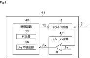
- the communication device 41 of the present embodiment includes a receiver circuit 42 instead of the receiver circuit 5 with respect to the communication device 2 of the first embodiment, and a control circuit instead of the control circuit 6. It is different in that it has 43.
- the receiver circuit 42 is different from the receiver circuit 5 shown in FIG. 3 in that the filter circuit 7 is omitted. In this case, the signal of the bus 3 is directly given to the non-inverting input terminal of the comparator 8.
- the control circuit 43 has functions as a determination unit 44 and a noise detection unit 45.
- the determination unit 44 determines the code transmitted via the bus 3 by sampling the signal of the bus 3 at a predetermined sampling timing.
- the noise detection unit 45 detects the signal level of the bus 3 and detects the noise superimposed on the bus 3 based on the detection result. Specifically, each of these functions is realized as follows.
- the control circuit 43 includes a digital filter circuit including an addition / subtraction counter that adds or subtracts based on the level of the received signal RX which is the output signal of the comparator 8.
- the addition / subtraction counter adds when the signal RX1 obtained by passing the received signal RX through the double matching filter included in the digital filter circuit is at a high level, and subtracts when the signal RX1 is at a low level. I do.
- the count value ct of the addition / subtraction counter is added when the signal RX1 is at a high level and is subtracted when the signal RX1 is at a low level.
- the signal RX2 corresponding to the received signal RX is generated based on the count value ct of such an addition / subtraction counter.
- the signal RX2 is a signal that turns to a low level when the count value ct reaches the lower limit value and turns to a high level when the count value ct reaches the upper limit value.
- the determination unit 44 determines the code transmitted via the bus 3 by sampling the signal RX2 generated in this way at a predetermined sampling timing.
- the sampling timing this time is determined according to the time obtained by adding a predetermined specified time corresponding to 6% of the bit rate to the previous Lo width.
- the sampling timing of this time is the time when the time obtained by adding the specified time to the previous Lo width elapses from the time of falling of the signal RX2 this time.
- addition / subtraction counter when noise is not superimposed on the bus 3, once subtraction is started, subtraction is continuously performed for a predetermined period thereafter, and once addition is started, after that. The addition is continuously performed for the predetermined period of.
- chattering occurs in the output of the comparator 8 due to noise superimposed on the bus 3 and the level of the received signal RX fluctuates, the addition / subtraction counter repeats addition and subtraction.
- the noise detection unit 45 determines that noise is superimposed on the bus 3 when the addition and subtraction by the addition / subtraction counter are repeatedly performed. Further, the noise detection unit 45 determines that the periods TNf and TNr in which the count value ct of the addition / subtraction counter increases / decreases are the noise detection periods in which the noise is detected.
- the Lo width described above accurately represents the low period at which the signal of the bus 3 is at the low level in the normal state where noise is not superimposed on the bus 3, but when noise is superimposed on the bus 3, it becomes the actual low period. Can be different. Specifically, when the received signal RX corresponding to the vicinity of the falling edge of the signal of the bus 3 fluctuates due to the influence of noise, the time until the count value ct reaches the lower limit value is delayed, and as a result, the signal RX2 Lo width becomes shorter than the actual row period.
- the received signal RX corresponding to the vicinity of the rising edge of the signal of the bus 3 fluctuates due to the influence of noise, the time until the count value ct reaches the upper limit value is delayed, and as a result, the Lo width of the signal RX2 becomes large. It will be longer than the actual row period.
- the sampling timing this time is determined based on the previous Lo width shorter than the actual row period, but the Lo width this time accurately represents the actual row period. Therefore, in the first case, the sampling timing this time is a timing that is ahead of the original timing, and as a result, it is erroneously determined that the signal of the bus 3 is at a low level even though it is at a high level. There is a risk.
- the sampling timing this time is determined based on the previous Lo width that accurately represents the actual row period, but the Lo width this time is longer than the actual row period. Therefore, even though the signal of the bus 3 is high level, it may be erroneously determined to be low level.
- the determination unit 44 delays the sampling timing by a predetermined time according to the period in which the noise is detected.
- the predetermined time is a period in which the above-mentioned period TNf and the period TNr are added.
- the delay time required from the boundary edge to the time when the transistor Q1 is turned on is shortened as compared with the configuration of the first embodiment. There is a merit that it is done.
- the filter circuit 7 for removing noise is not provided, there is a demerit that the possibility of erroneous determination due to the influence of noise increases.
- the present embodiment since the occurrence of erroneous determination due to the influence of noise is prevented as described above, there is no demerit due to the absence of the filter circuit 7, and only the merit is enjoyed. be able to.
- FIGS. 11 to 13 a fifth embodiment in which the specific configurations of the driver circuit and the control circuit have been changed with respect to the first embodiment will be described with reference to FIGS. 11 to 13.
- the driver circuit 51 of the present embodiment is different from the driver circuit 4 of the first embodiment shown in FIG. 4 in that the drive circuit 52 is provided in place of the drive circuit 9. There is.
- the drive circuit 52 is different from the drive circuit 9 in that the delay shortening unit 14 is omitted and that the switch S51 is provided instead of the transistor Q5.
- One terminal of the switch S51 is connected to the power supply line L2, and the other terminal is connected to the node N2 via the current source 11.
- the on / off of the switch S51 is controlled by the transmission signal TX.
- the switch S51 is turned off when the transmission signal TX is at a high level and is turned on when the transmission signal TX is at a low level.
- the switch S51 can be configured by using a semiconductor switching element such as a MOS transistor.
- the current source 12 is configured so that its operation can be stopped. Specifically, the current source 12 stops the operation during the period when the cut signal PSCM, which will be described later, is at a high level, and executes the operation during the period when the cut signal PSCM is at a low level.
- the control circuit 53 of the present embodiment has functions as a learning control unit 54, a predictive control unit 55, and a first-out control unit 56.
- the learning control unit 54 executes learning control for learning the period of the boundary edge based on the detection result of the boundary edge by the receiver circuit 5 functioning as the edge detection circuit.
- the learning control unit 54 includes a counter 54a, which is a hardware timer counter that measures a 1-bit rate.
- the counter 54a executes the counting operation from the time when the boundary edge is detected to the time when the boundary edge is detected next.
- the counter 54a starts the counting operation when the boundary edge is detected, and thereafter restarts the counting operation after clearing the count value at each time when the boundary edge is detected.
- the learning control unit 54 learns the period of the boundary edge based on the count value of the counter 54a. That is, the learning control unit 54 learns the count value when the counter 54a is cleared as the learning value of the boundary edge cycle each time. Since the bit rate is constant, such a learning value shows a constant value. For example, when the bit rate is 20 kbps and the counter 54a operates with a system clock of 4.5 MHz, the learning value is constant at "225".
- the prediction control unit 55 executes predictive control that predicts the timing at which the next boundary edge is detected based on the cycle of the boundary edge learned by the learning control unit 54 executing the learning control. Specifically, the prediction control unit 55 can predict the timing at which the next boundary edge is detected based on the learning value learned by the learning control and the current count value of the counter 54a.
- the first-out control unit 56 executes first-out control that gives an on-command to the drive circuit 52, that is, a low-level transmission signal TX at a time point earlier than the timing predicted by the prediction control unit 55 executing the prediction control. .. Specifically, the advance control unit 56 starts outputting the low-level transmission signal TX at a time point that is a predetermined number of clocks before the time point when the count value of the counter 54a matches the learning value.
- the advance control unit 56 starts outputting the low-level transmission signal TX when the count value of the counter 54a is "220" and the counter matches. ing.
- the setting of the predetermined number of clocks that is, the setting of how much before the predicted timing to start the output, can be appropriately changed and adjusted according to various specifications and the like.
- the delay time required from the boundary edge to the time when the transistor Q1 is turned on is shortened by executing each of the above-mentioned controls by the learning control unit 54, the predictive control unit 55, and the advance control unit 56. .. That is, in this case, the delay shortening unit 57 is configured by the learning control unit 54, the prediction control unit 55, and the advance control unit 56. As described above, in the present embodiment, the delay shortening unit 57 is provided in the control circuit 53.
- the control circuit 53 generates the cut signal PSCM described above.
- the cut signal PSCM is high in the first-out period, which is the period from the time when the output of the low-level transmission signal TX is started by executing the first-out control to the timing when the next boundary edge predicted by the prediction control is detected. It becomes a level and becomes a low level in other periods.
- the operation of each part during the off period in which the drive circuit 52 drives the transistor Q1 off is as follows. That is, since the transmission signal TXS is at a high level, the switch S51 is turned off. As a result, the gate-source capacitance of the transistor Q1 is discharged by the current of the current source 12, so that the gate voltage Vg drops and the transistor Q1 is turned off.
- the control circuit 53 executes each of the above-mentioned controls, so that the transmission signal is transmitted at a time point t51 before the time point t3 when the control circuit 6 of the first embodiment shifts the transmission signal TXS from the high level to the low level. Turn TXS from high level to low level. During the period after the time point t51, the transmission signal TXS becomes a low level. During such a period, the drive circuit 52 drives the transistor Q1 on. The operation of each part during the ON period in which the drive circuit 52 drives the transistor Q1 on is as follows.
- the switch S51 since the transmission signal TXS is at a low level, the switch S51 is turned on. Further, the cut signal PSCM becomes a high level during the advance period from the time point t51 to the time point t3. Therefore, during the first-out period, the output current of the current source 11 branches and flows so as to charge each of the capacitors C1 and C2. After that, when the cut signal PSCM turns to a low level at the time point t3, a current having a current value I2 corresponding to the difference between the output current of the current source 11 and the output current of the current source 12 is supplied toward the gate of the transistor Q1. It will be.
- the gate voltage Vg of the transistor Q1 rises relatively gently with a constant slope from the time point t52 when a short time has passed from the time point t51.
- the slope of the increase in the gate voltage Vg at this time is determined by the current values I1 and I2 of the current sources 11 and 12 and the capacitance values of the capacitors C1 and C2. Then, at the time t53 when the gate voltage Vg of the transistor Q1 reaches the threshold voltage Vt, the transistor Q1 is turned on.
- the present embodiment described above also includes the delay shortening unit 57 that shortens the delay time required from the boundary edge to the time when the transistor Q1 is turned on, the same effect as that of the first embodiment can be obtained.
- the delay shortening unit 57 provided in the control circuit 53 executes various controls to switch the transmission signal TX to the low level at a timing ahead of the comparative example corresponding to the conventional configuration. .. Therefore, according to the present embodiment, by setting the timing for advancing the transmission signal TX, not only the delay time due to the operation of the drive circuit 52, but also the logic delay in the control circuit 53, the delay in the filter circuit 7, and the comparator 8 It is possible to significantly reduce the overall delay time including the delay in.
- the drive circuit 52 of the present embodiment has a configuration in which the transistor Q1 is driven on by constant current drive throughout the on period, as in the comparative example described in the first embodiment. Therefore, in the present embodiment, the gate voltage rises relatively slowly to reach the threshold voltage Vt, and the transistor Q1 is turned on. Therefore, according to the present embodiment, it is possible to reduce the risk of deterioration of emissions due to the ON operation of the transistor Q1.
- the control circuit 53 does not start the output of the low-level transmission signal TXS triggered by the change of the signal of the bus 3, but is based on the learned value of the learned boundary edge period.
- the output of the low-level transmission signal TXS is started ahead of schedule, and there is no need to wait for a change in the signal of the bus 3. That is, the control circuit 53 starts to output the low-level transmission signal TXS when the dominant code is output even if the clock is not output from the master 2m.
- the control circuit 53 outputs the low level transmission signal TXS based on the learning value. That is, there is a possibility that the signal level of the bus 3 is changed and the behavior is as if the clock from the master 2 m is supplied. Therefore, in the configuration of the fifth embodiment, even if the bus 3 is fixed at a high level, the slave 2s may run by itself when continuously outputting the dominant code. In the following, the sticking of the bus 3 to a high level is referred to as Hi sticking.
- the UART frame is decoded and a signal is put on the bus 3.
- the UART always contains at least one stop bit. Therefore, in the operation of the slave 2s, the timing of outputting the recessive code corresponding to "logical value: 1" to the bus 3 is always included.
- the control circuit 53 When the slave 2s outputs the recessive code corresponding to the stop bit when the bus 3 is fixed to Hi, the boundary edge is not detected for a relatively long period of time. Therefore, the count value of the counter 54a is assumed as the period of the boundary edge. It is a very large value compared to the value (for example) "225"). Therefore, when the count value of the counter 54a reaches an upper limit value (for example, “1024”) larger than the value assumed as the period of the boundary edge, the control circuit 53 once resets the learning result by the learning control to perform the learning control. It is supposed to be executed again.
- the control circuit 53 stops the execution of the predictive control and the first-out control until the learning result by the learning control is obtained.
- the control circuit 53 includes a remeasurement counter that counts the number of times that the learning value is correctly obtained, and the period until the count value of the remeasurement counter becomes "3", that is, the learning value is The execution of the predictive control and the first-out control is stopped until three times are obtained.
- the count value of the counter 54a is cnt1
- the count value of the remeasurement counter is cnt2.
- the slave 2s In the period Ta, the slave 2s is in a state of continuously outputting the dominant code. Therefore, the slave 2s outputs the low-level transmission signal TXS based on the learning value even though the clock supply is stopped from the master 2m, that is, the signal level of the bus 3 is changed.
- the count value ct1 is "230", "235”, etc., and the cycle of the boundary edge. The value does not deviate significantly from the value assumed as.
- the slave 2s In the period Tb, the slave 2s is in a state of outputting a recessive code corresponding to, for example, a stop bit. Therefore, the count value ct1 of the counter 54a rises beyond the value assumed as the period of the boundary edge, and reaches the upper limit value “1024”. As a result, the control circuit 53 once resets the learning result of the learning control, executes the learning control again, and stops the execution of the predictive control and the first-out control. In FIG. 14, such an operating state is represented as a reset operation (during remeasurement). At this time, the count value of the remeasurement counter is cleared to "0".
- the clock supply is restarted from the master 2m.
- the learning value starts to be normally obtained by the learning control, and when the learning value is obtained three times, the control circuit 53 resumes the execution of the prediction control and the advance control.
- the slave 2s is in a normal operating state in which the slave 2s operates in synchronization with the clock from the master 2m. In FIG. 14, such an operating state is represented as a reset release operation.
- the control circuit 53 will perform the control circuit 53 when the count value of the counter 54a reaches the upper limit. Since it is determined that the bus 3 is fixed to Hi and the execution of the predictive control and the advance control is stopped, there is no possibility that the slave 2s will continue to operate without synchronizing with the clock supplied from the master 2m. Further, in this case, when the control circuit 53 determines that the bus 3 is fixed to Hi, the learning value is reset and the learning control is restarted, and when the learned value is correctly obtained by the restarted learning control, the prediction control and The first-out control is restarted. Therefore, when the abnormality on the master 2m side is resolved, the slave 2s can promptly resume the prediction control and the first-out control, and can return to the normal operation.
- the present disclosure is not limited to the communication devices 2 and 41 that perform CXPI communication exemplified in each of the above embodiments, and is synchronized with the communication of any one of a plurality of communication devices that transmit and receive data via a transmission line. It can be applied to all communication devices used in communication systems in which other communication devices transmit.
- the switching element provided in the output stage of the driver circuit 4 or the like is not limited to a MOS transistor such as the transistor Q1, and various semiconductor switching elements such as a bipolar transistor and a GaAs-MESFET can be used.
Landscapes
- Engineering & Computer Science (AREA)
- Computer Networks & Wireless Communication (AREA)
- Signal Processing (AREA)
- Physics & Mathematics (AREA)
- Nonlinear Science (AREA)
- Computer Hardware Design (AREA)
- Computing Systems (AREA)
- General Engineering & Computer Science (AREA)
- Mathematical Physics (AREA)
- Power Engineering (AREA)
- Logic Circuits (AREA)
- Dc Digital Transmission (AREA)
Abstract
通信装置は、伝送路を介してデータを送受信する複数の通信装置のうちいずれか一つの通信装置の通信に同期して他の通信装置が送信を行う通信システムにて用いられるもので、前記伝送路の信号レベルが劣位レベルから優位レベルに変化するエッジを検出するエッジ検出回路(5、42)と、オンすることにより前記伝送路の信号レベルを前記優位レベルとすることができるスイッチング素子(Q1)と、前記スイッチング素子を駆動する駆動回路(9、22、32、52)と、前記駆動回路の動作を制御するものであり前記エッジ検出回路により前記エッジが検出されると前記駆動回路に対して前記スイッチング素子のオン駆動を指令するオン指令を与える制御回路(6、43、53)と、を備える。前記駆動回路または前記制御回路には、前記エッジから前記スイッチング素子がオンする時点までに要する遅延時間を短縮する遅延短縮部(14、23、34、57)が設けられる。
Description
本出願は、2019年8月30日に出願された日本出願番号2019-158359号に基づくもので、ここにその記載内容を援用する。
本開示は、伝送路を介してデータを送受信する複数の通信装置のうちいずれか一つの通信装置の通信に同期して他の通信装置が送信を行う通信システムにおいて用いられる通信装置に関する。
従来、車両に搭載された車載通信の方式として、例えばCXPIなど、マスタの通信に同期してスレーブが送信を行う通信方式が知られている。なお、CXPIとは、Clock Extension Peripheral Interfaceの略称である。特許文献1には、このような通信において、伝送路上で優位な信号レベルを優位レベルとするとともに劣位な信号レベルを劣位レベルとしたとき、伝送路の信号レベルを劣位レベルから優位レベルに変化させるときのドライバ回路の動作を高速化させるための技術が開示されている。
このような通信において、マスタにより生成されるクロックのエッジから伝送路の信号レベルを劣位レベルから優位レベルに変化させる時点までの遅延時間は、通信プロトコルを満足しなければならないことから極力短いほうが望ましい。その一方で、ノイズ対策として、受信バッファの前段にフィルタ回路を挿入したという要望がある。しかし、フィルタ回路を挿入すると、その影響により、遅延時間が長くなり、通信プロトコルを満足できなくなるおそれが生じる。
本開示の目的は、遅延時間を短縮することができる通信装置を提供することにある。
本開示の一態様において、通信装置は、伝送路を介してデータを送受信する複数の通信装置のうちいずれか一つの通信装置の通信に同期して他の通信装置が送信を行う通信システムにおいて用いられる通信装置であり、エッジ検出回路、スイッチング素子、駆動回路および制御回路を備える。この場合、伝送路上で優位な信号レベルを優位レベルとし、劣位な信号レベルを劣位レベルとする。エッジ検出回路は、伝送路の信号レベルが劣位レベルから優位レベルに変化するエッジを検出する。スイッチング素子は、オンすることにより伝送路の信号レベルを優位レベルとすることができる。駆動回路は、スイッチング素子を駆動する。制御回路は、駆動回路の動作を制御するものであり、エッジ検出回路によりエッジが検出されると駆動回路に対してスイッチング素子のオン駆動を指令するオン指令を与える。
上記構成において、駆動回路または制御回路には、伝送路の信号レベルが劣位レベルから優位レベルに変化するエッジからスイッチング素子がオンする時点までに要する遅延時間を短縮する遅延短縮部が設けられている。したがって、上記構成によれば、遅延時間を短縮することが可能となり、受信バッファの前段にフィルタ回路を挿入するような場合であっても、通信プロトコルを十分に満足することができる。
本開示の一態様において、通信装置では、遅延短縮部は、駆動回路に設けられたものである。この場合、遅延短縮部は、駆動回路がスイッチング素子をオン駆動するオン期間の開始時点を含む期間に、スイッチング素子の制御端子の電圧である制御電圧が、スイッチング素子がオンに転じる閾値電圧よりも所定値だけ低い第1電圧まで上昇するように電圧制御を行うことで遅延時間を短縮する。
例えば、スイッチング素子をオン期間を通じて定電流駆動によりオン駆動するような従来の構成では、スイッチング素子の制御電圧は、オン期間を通じて一定の傾きで比較的緩やかに上昇する。そのため、上記した従来の構成では、制御電圧が閾値電圧に達してスイッチング素子がオンに転じるまでには、比較的長い時間を要することになり、その結果、駆動回路の動作に起因する遅延時間が長くなるおそれがある。これに対し、上記構成では、前述した電圧制御が行われることにより、スイッチング素子の制御電圧は、オン期間の開始時点を含む期間に第1電圧まで比較的急峻に一度に上昇する。
上記構成では、このような電圧制御を行うことにより制御電圧が第1電圧まで上昇した後は、本開示の一態様における定電流制御が行われることにより、または、本開示の一態様における電圧制御が継続されることにより、制御電圧が閾値電圧に達してスイッチング素子がオンに転じる。このような構成によれば、上記した従来の構成に比べ、少なくとも制御電圧が第1電圧まで一度に上昇される分だけ、スイッチング素子のターンオン時間、つまり駆動回路の動作に起因する遅延時間が短縮される。
本開示の一態様において、通信装置では、遅延短縮部が設けられた駆動回路は、電圧制御を行うことにより制御電圧が第1電圧まで上昇した後、スイッチング素子の制御端子に一定の電流を供給する定電流制御を行う。このような構成によれば、スイッチング素子の制御電圧は、第1電圧まで上昇した後は、一定の傾きで比較的緩やかに上昇して閾値電圧に達することになる。制御電圧が急峻に上昇して閾値電圧に達してスイッチング素子がオンされると、そのオン動作に伴うエミッションの悪化が懸念される。しかし、上記構成によれば、制御電圧が比較的緩やかに上昇して閾値電圧に達してスイッチング素子がオンされるため、このようなエミッション悪化のリスクが軽減される。
本開示についての上記目的およびその他の目的、特徴や利点は、添付の図面を参照しながら下記の詳細な記述により、より明確になる。その図面は、
図1は、第1実施形態に係る通信システムの構成を模式的に示す図であり、
図2は、第1実施形態に係る通信装置の構成を模式的に示す図であり、
図3は、第1実施形態に係るレシーバ回路の具体的な構成を模式的に示す図であり、
図4は、第1実施形態に係るドライバ回路の具体的な構成を模式的に示す図であり、
図5は、第1実施形態に係る通信装置の動作を説明するための図であり、送信信号、バス波形およびゲート電圧を模式的に示すタイミングチャートであり、
図6は、第2実施形態に係るドライバ回路の具体的な構成を模式的に示す図であり、
図7は、第3実施形態に係るドライバ回路の具体的な構成を模式的に示す図であり、
図8は、第3実施形態に係る通信装置の動作を説明するための図であり、送信信号、バス波形およびゲート電圧を模式的に示すタイミングチャートであり、
図9は、第4実施形態に係る通信装置の構成を模式的に示す図であり、
図10は、第4実施形態に係る制御回路における各信号および加減算カウンタのカウント値を模式的に示すタイミングチャートであり、
図11は、第5実施形態に係るドライバ回路の具体的な構成を模式的に示す図であり、
図12は、第5実施形態に係る制御回路の具体的な構成を模式的に示す図であり、
図13は、第5実施形態に係る通信装置の動作を説明するための図であり、送信信号、バス波形およびゲート電圧を模式的に示すタイミングチャートであり、
図14は、第6実施形態に係るバスがハイレベルに固着した場合の動作を説明するための図であり、送信信号、バス波形、カウント値および制御回路の動作状態を模式的に示すタイミングチャートである。
以下、複数の実施形態について図面を参照して説明する。なお、各実施形態において実質的に同一の構成には同一の符号を付して説明を省略する。
(第1実施形態)
以下、第1実施形態について図1~図5を参照して説明する。
(第1実施形態)
以下、第1実施形態について図1~図5を参照して説明する。
<通信システムの構成について>
図1に示す通信システム1は、例えば車両に搭載された複数の電子制御装置間の制御通信のために用いられるものである。通信システム1は、複数の通信装置2a、2b、2cが伝送路に相当するバス3を介して接続された構成となっている。以下では、通信装置2a、2b、2cについて、それぞれを区別する必要がない場合には通信装置2と総称することとする。この場合、通信システム1は、3つの通信装置2を備えているが、2つの通信装置2を備えていてもよいし、4つ以上の通信装置2を備えていてもよい。
図1に示す通信システム1は、例えば車両に搭載された複数の電子制御装置間の制御通信のために用いられるものである。通信システム1は、複数の通信装置2a、2b、2cが伝送路に相当するバス3を介して接続された構成となっている。以下では、通信装置2a、2b、2cについて、それぞれを区別する必要がない場合には通信装置2と総称することとする。この場合、通信システム1は、3つの通信装置2を備えているが、2つの通信装置2を備えていてもよいし、4つ以上の通信装置2を備えていてもよい。
複数の通信装置2は、半導体集積回路、つまりICとして構成されており、バス3を介してデータを送受信する。通信システム1では、複数の通信装置2のうちいずれか一つの通信装置2、具体的には通信装置2aの通信に同期して他の通信装置2b、2cが送信を行うようになっている。以下では、通信装置2aのことをマスター2mとも称するとともに、通信装置2b、2cのことをスレーブ2sとも称することとする。
通信システム1では、CXPI通信によりデータの送受信が実行されるようになっている。CXPI通信では、マスター2mは、スレーブ2sにバス3を介してクロックを供給し、スレーブ2sは、バス3を介して供給されるクロックに同期した通信を実行する。この場合、バス3は、異なる通信装置2からハイレベルの信号とロウレベルの信号とが同時に出力されると、バス3上の信号レベルがロウレベルとなるように構成されており、この機能を利用してバス調停が実現される。すなわち、この場合、ロウレベルの信号がバス3上で優位な信号レベルである優位レベルに相当し、ハイレベルの信号がバス3上で劣位な信号レベルである劣位レベルに相当する。
バス3上では、伝送路符号として、ビットの境界で信号レベルがハイレベルからロウレベルに変化するとともに、ビットの途中で信号レベルがロウレベルからハイレベルに変化するパルス幅変調信号、つまりPWM信号が用いられ、二値の信号が、デューティ比の異なる二種類のPWM信号で表現される。以下では、ロウレベルの期間が比較的短いほうをレセッシブ符号と称するとともに、ロウレベルの期間が比較的長いほうをドミナント符号と称する。レセッシブ符号は「論理値=1」に対応し、ドミナント符号は「論理値=0」に対応する。
この場合、レセッシブ符号では、1ビットの最初の1/3の期間がロウレベルになるとともに、その後の2/3の期間がハイレベルになるように設定されている。また、この場合、ドミナント符号では、1ビットの最初の2/3の期間がロウレベルになるとともに、その後の1/3の期間がハイレベルになるように設定されている。このようなことから、バス3上でレセッシブ符号とドミナント符号とが衝突すると、ドミナント符号が調停勝ちするようになっている。
<通信装置の構成について>
マスター2mとスレーブ2sとは、クロックを供給するための構成の有無など一部構成が異なるが、概ね同様の構成を有している。すなわち、図2に示すように、通信装置2は、ドライバ回路4、レシーバ回路5および制御回路6を備えている。ドライバ回路4には、制御回路6から出力される送信信号TXが与えられている。
マスター2mとスレーブ2sとは、クロックを供給するための構成の有無など一部構成が異なるが、概ね同様の構成を有している。すなわち、図2に示すように、通信装置2は、ドライバ回路4、レシーバ回路5および制御回路6を備えている。ドライバ回路4には、制御回路6から出力される送信信号TXが与えられている。
ドライバ回路4は、送信信号TXに応じたデータをバス3を介して送信する。レシーバ回路5は、バス3を介して送信されたデータを受信し、受信信号RXとして制御回路6へ出力する。制御回路6は、ロジック回路として構成されたものであり、送信信号TXを生成し、その送信信号TXをドライバ回路4に出力する。また、制御回路6は、レシーバ回路5から出力される受信信号RXを入力し、その入力した受信信号RXに基づいて所定の処理を実行する。
<レシーバ回路の具体的な構成について>
図3に示すように、レシーバ回路5は、フィルタ回路7およびコンパレータ8を備えている。この場合、バス3の信号は、フィルタ回路7を介してコンパレータ8の非反転入力端子に与えられている。フィルタ回路7は、例えば低域通過フィルタ、つまりLPFなどであり、ノイズ対策として挿入されたものである。フィルタ回路7の出力信号は、バス3の信号に対し、ノイズが除去されるとともにフィルタ回路7の時定数に応じた遅れが生じた信号となる。
図3に示すように、レシーバ回路5は、フィルタ回路7およびコンパレータ8を備えている。この場合、バス3の信号は、フィルタ回路7を介してコンパレータ8の非反転入力端子に与えられている。フィルタ回路7は、例えば低域通過フィルタ、つまりLPFなどであり、ノイズ対策として挿入されたものである。フィルタ回路7の出力信号は、バス3の信号に対し、ノイズが除去されるとともにフィルタ回路7の時定数に応じた遅れが生じた信号となる。
コンパレータ8の反転入力端子には、閾値信号Saが与えられている。閾値信号Saは、バス3の信号レベルがハイレベルからロウレベルに変化するエッジを検出するための閾値Thに対応した信号である。以下、このようなエッジのことを境界エッジとも称する。このような構成により、コンパレータ8は、バス3の信号レベルが閾値Thより高い場合にはハイレベルの信号を出力するとともに、バス3の信号レベルが閾値Thより低い場合にはロウレベルの信号を出力するようになっている。コンパレータ8の出力信号は、前述した受信信号RXとして制御回路6に与えられる。
上記構成のレシーバ回路5は、バス3の信号レベルがハイレベルからロウレベルに変化するエッジ、つまり境界エッジを検出することができる。具体的には、レシーバ回路5は、コンパレータ8の出力信号である受信信号RXがハイレベルからロウレベルへと転じたことをもって境界エッジを検出することができる。このように、本実施形態では、レシーバ回路5は、エッジ検出回路としての機能を有する。
<ドライバ回路の具体的な構成について>
図4に示すように、ドライバ回路4は、前述したバス調停が可能となるように、オープンドレイン出力の回路構成となっており、その出力段を構成するトランジスタQ1、ダイオードD1、D2、抵抗R1および駆動回路9を備えている。ドライバ回路4において、バス3にはダイオードD1のカソードが接続されている。ダイオードD1のアノードは、プルアップ用の抵抗R1を介して電源電圧Vaが供給される電源線L1に接続されている。電源電圧Vaは、車両に搭載されるバッテリーの電源+Bから生成される+B系の電源電圧である。
図4に示すように、ドライバ回路4は、前述したバス調停が可能となるように、オープンドレイン出力の回路構成となっており、その出力段を構成するトランジスタQ1、ダイオードD1、D2、抵抗R1および駆動回路9を備えている。ドライバ回路4において、バス3にはダイオードD1のカソードが接続されている。ダイオードD1のアノードは、プルアップ用の抵抗R1を介して電源電圧Vaが供給される電源線L1に接続されている。電源電圧Vaは、車両に搭載されるバッテリーの電源+Bから生成される+B系の電源電圧である。
トランジスタQ1は、Nチャネル型のMOSトランジスタであり、そのドレインはダイオードD2を逆方向に介してバス3に接続されている。トランジスタQ1のソースは、回路の基準電位(0V)となるグランドに接続されている。トランジスタQ1は、オンすることによりバス3の信号レベルをロウレベル(0V)とすることができるスイッチング素子として機能する。
駆動回路9は、制御回路6から与えられる送信信号TXに基づいてトランジスタQ1を駆動する。言い換えると、駆動回路9の動作は、制御回路6により制御される。駆動回路9は、トランジスタQ2~Q5、ダイオードD3、電流源10~12、コンデンサC1、C2、抵抗R2およびゲートドライバ13を備えている。トランジスタQ2は、Nチャネル型のMOSトランジスタであり、そのゲートには送信信号TXが与えられている。トランジスタQ2のソースはグランドに接続され、そのドレインはノードN1に接続されている。
トランジスタQ3は、Nチャネル型のMOSトランジスタであり、そのソースはダイオードD3を順方向に介してグランドに接続されている。トランジスタQ3は、いわゆるダイオード接続されており、そのゲートおよびドレインは、共通接続されるとともにノードN1に接続されている。電流源10は、電源電圧Vbが供給される電源線L2とノードN1との間に接続されている。
電源電圧Vbは、例えば5V電源系など+B系の電源電圧とは別系統の電源電圧である。なお、電源電圧Vbは、+B系の電源電圧であってもよい。トランジスタQ4は、NPN形のバイポーラトランジスタであり、そのベースはノードN1に接続されている。トランジスタQ4のコレクタは電源線L2に接続され、そのエミッタはノードN2に接続されている。トランジスタQ5は、Pチャネル型のMOSトランジスタであり、そのゲートには送信信号TXが与えられている。
トランジスタQ5のソースは電源線L2に接続され、そのドレインは電流源11を介してノードN2に接続されている。電流源12は、ノードN2とグランドとの間に接続されている。本実施形態では、電流源11は、電流源12に対して例えば2倍の電流を出力するようになっている。すなわち、電流源11の電流値I1と、電流源12の電流値I2と、は、例えば下記(1)式に示す関係となっている。
I1=2×I2…(1)
I1=2×I2…(1)
コンデンサC1の一方の端子は、抵抗R2を介してダイオードD1のアノードに接続されている。コンデンサC1の他方の端子は、ノードN2に接続されている。コンデンサC2は、ノードN2とグランドとの間に接続されている。この場合、コンデンサC1、C2は、静電容量値が互いに同一のものが用いられている。ゲートドライバ13は、単なるバッファとして機能するものであり、その入力端子はノードN2に接続されており、その出力端子はトランジスタQ1のゲートに接続されている。この場合、トランジスタQ1のゲートがスイッチング素子の制御端子に相当し、ゲート電圧が制御電圧に相当する。
制御回路6から出力される送信信号TXは、2値の信号であり、ハイレベルのときにはトランジスタQ1のオフ駆動を指令するオフ指令となり、ロウレベルのときにはトランジスタQ1のオン駆動を指令するオン指令となる。この場合、送信信号TXのハイレベルは、トランジスタQ2をオンするとともにトランジスタQ5をオフすることができる電圧値であり、例えば電源電圧Vbと同等の電圧値となっている。また、送信信号TXのロウレベルは、トランジスタQ2をオフするとともにトランジスタQ5をオンすることができる電圧値であり、例えば0Vとなっている。
<遅延短縮部について>
CXPI通信では、マスター2mは、常にレセッシブ符号を出力しており、これが前述したクロックとなる。スレーブ2sは、このクロックに同期して動作する。具体的には、スレーブ2sは、レシーバ回路5により前述したようにして境界エッジが検出されたタイミング、つまりクロックの立ち下がりエッジが検出されたタイミングに同期して動作する。スレーブ2sでは、制御回路6は、境界エッジが検出されると、駆動回路9に対してロウレベルの送信信号TXを与える。そして、駆動回路9は、ロウレベルの送信信号TXが与えられるとトランジスタQ1をオン駆動する。
CXPI通信では、マスター2mは、常にレセッシブ符号を出力しており、これが前述したクロックとなる。スレーブ2sは、このクロックに同期して動作する。具体的には、スレーブ2sは、レシーバ回路5により前述したようにして境界エッジが検出されたタイミング、つまりクロックの立ち下がりエッジが検出されたタイミングに同期して動作する。スレーブ2sでは、制御回路6は、境界エッジが検出されると、駆動回路9に対してロウレベルの送信信号TXを与える。そして、駆動回路9は、ロウレベルの送信信号TXが与えられるとトランジスタQ1をオン駆動する。
ただし、上記構成では、バス3上の信号レベルがハイレベルからロウレベルに変化したタイミング、つまりクロックの立ち下がりタイミングである境界エッジからトランジスタQ1のゲート電圧が閾値電圧Vt(Q1)に達してトランジスタQ1がオンする時点までに要する時間である遅延時間が存在する。この遅延時間は、フィルタ回路7での遅延、コンパレータ8での遅延、制御回路6におけるロジック遅延およびドライバ回路4の回路動作に伴う遅延などにより定まる時間となる。このような遅延時間は、CXPIの通信プロトコルにより規定された時間(例えば0.11Tbit)を満足する必要がある。なお、1Tbitは、バスのボーレート周期である。
上記構成では、レシーバ回路5の前段にノイズ除去用のフィルタ回路7が挿入されており、このようなフィルタ回路が設けられていない構成に比べて遅延時間が長くなる。そこで、本実施形態の通信装置2には、このような遅延時間を短縮するための遅延短縮部14が設けられている。この場合、駆動回路9のトランジスタQ2、Q3、Q4、ダイオードD3および電流源10により、遅延短縮部14が構成されている。つまり、本実施形態では、遅延短縮部14は、駆動回路9に設けられている。
また、この場合、トランジスタQ3は、その閾値電圧Vt(Q3)が、トランジスタQ1がオンに転じる閾値電圧Vt(Q1)に対して所定値αだけ低いものが用いられている。すなわち、閾値電圧Vt(Q3)と閾値電圧Vt(Q1)との関係は、下記(2)式により表される。
Vt(Q3)=Vt(Q1)-α (2)
Vt(Q3)=Vt(Q1)-α (2)
詳細は後述するが、遅延短縮部14は、駆動回路9がトランジスタQ1をオン駆動するオン期間の開始時点を含む期間に、トランジスタQ1のゲート電圧が、閾値電圧Vt(Q1)よりも所定値αだけ低い閾値電圧Vt(Q3)まで上昇するように電圧制御を行うことで遅延時間を短縮するようになっている。なお、この場合、閾値電圧Vt(Q3)が第1電圧V1に相当する。また、このような遅延短縮部14が設けられた駆動回路9は、上記した電圧制御が行われることによりトランジスタQ1のゲート電圧が閾値電圧Vt(Q3)まで上昇した後、トランジスタQ1のゲートに一定の電流を供給する定電流制御を行うようになっている。
次に、上記構成の作用について図5のタイミングチャートに基づいて説明する。なお、図5などでは、マスター2mにおける送信信号TXを送信信号TXMと称し、スレーブ2sにおける送信信号TXを送信信号TXSと称し、トランジスタQ1のゲート電圧をVgと称し、トランジスタQ1の閾値電圧Vt(Q1)をVtと称している。また、図5などのタイミングチャートでは、2値の信号について、ロウレベルを「L」と称し、ハイレベルを「H」と称している。
この場合、送信信号TXMがハイレベルからロウレベルに転じる時点t1がクロックの立ち下がりであり、境界エッジに相当する。時点t1以前の期間、送信信号TXSはハイレベルとなっている。このような期間、駆動回路9は、トランジスタQ1をオフ駆動する。駆動回路9がトランジスタQ1をオフ駆動するオフ期間における各部の動作は、次のようなものとなる。
すなわち、送信信号TXSがハイレベルであることから、トランジスタQ2がオンするとともにトランジスタQ5がオフする。トランジスタQ5がオフすることから、電流源12の電流によりトランジスタQ1のゲート・ソース間容量が放電されることでゲート電圧Vgが低下してトランジスタQ1がオフする。そのため、時点t1以前の期間、バス3の信号レベルはハイレベルに維持されている。また、トランジスタQ2がオンすることから、トランジスタQ3、Q4がオフする。そのため、遅延短縮部14は、ノードN2の電圧VN2ひいてはトランジスタQ1のゲート電圧Vgに何ら影響を及ぼさない。
時点t1において送信信号TXMがロウレベルに転じた後、バス3の信号レベルが低下して閾値Thに達した時点t2において、レシーバ回路5により境界エッジが検出される。なお、時点t1から時点t2までの時間には、マスター2m側での信号出力に関する遅延、フィルタ回路7およびコンパレータ8による遅延時間などが含まれる。このように境界エッジが検出されると、制御回路6は、送信信号TXSをハイレベルからロウレベルに転じさせる。なお、時点t2から送信信号TXSがロウレベルに転じる時点t3までの時間には、制御回路6によるロジック遅延などが含まれる。
時点t3以降の期間、送信信号TXSはロウレベルとなる。このような期間、駆動回路9は、トランジスタQ1をオン駆動する。駆動回路9がトランジスタQ1をオン駆動するオン期間における各部の動作は、次のようなものとなる。すなわち、送信信号TXSがロウレベルであることから、トランジスタQ2がオフするとともにトランジスタQ5がオンする。トランジスタQ2がオフすることから、トランジスタQ3、Q4がオンする。トランジスタQ3がオンすることから、電源線L2から電流源10、トランジスタQ3およびダイオードD3を介してグランドへと電流が流れる。
これにより、ノードN1の電圧VN1は、下記(3)式により表される電圧となる。ただし、ダイオードD3の順方向電圧をVfとする。
VN1=Vt(Q3)+Vf …(3)
これにより、ノードN1の電圧VN1は、下記(3)式により表される電圧となる。ただし、ダイオードD3の順方向電圧をVfとする。
VN1=Vt(Q3)+Vf …(3)
また、トランジスタQ4がオンすることから、トランジスタQ4のエミッタ電圧、つまりノードN2の電圧VN2は、下記(4)式により表される電圧となる。ただし、トランジスタQ4のベース・エミッタ間電圧Vbeが、ダイオードD3の順方向電圧Vfと同程度の電圧であるものとする。
VN2=Vt(Q3)=Vt(Q1)-α …(4)
VN2=Vt(Q3)=Vt(Q1)-α …(4)
上記構成では、トランジスタQ1のゲート電圧Vgは、電圧VN2と同等の電圧となる。そのため、トランジスタQ1のゲート電圧Vgは、時点t3から僅かな時間が経過した時点t4において、0Vから「Vt-α」へと急峻に上昇する。なお、時点t3から時点t4までの時間には、各トランジスタの動作に伴う遅延時間などが含まれる。
この場合、トランジスタQ5がオンしていることから、トランジスタQ1のゲートに向けて、電流源11の出力電流と電流源12の出力電流との差に相当する電流値I2の電流が供給されることになる。そのため、上述した電圧制御が行われることによりトランジスタQ1のゲート電圧Vgが「Vt-α」まで上昇した後、トランジスタQ1のゲートに対して一定の電流が供給される定電流制御が行われる。
このような定電流制御が行われることにより、トランジスタQ1のゲート電圧Vgは、時点t4から僅かな時間が経過した時点t5から一定の傾きで比較的緩やかに上昇する。このときのゲート電圧Vgの上昇の傾きは、電流源11、12の各電流値I1、I2およびコンデンサC1、C2の静電容量値などにより定まる。そして、トランジスタQ1のゲート電圧Vgが閾値電圧Vtに達した時点t6において、トランジスタQ1がオンする。
以上説明した本実施形態によれば、次のような効果が得られる。
本実施形態の通信装置2は、境界エッジからトランジスタQ1がオンする時点までに要する遅延時間を短縮する遅延短縮部14を備えている。このような構成によれば、遅延時間を短縮することが可能となり、本実施形態の構成のようにレシーバ回路5の前段にフィルタ回路7を挿入するような場合であっても、通信プロトコルを十分に満足することができる。
本実施形態の通信装置2は、境界エッジからトランジスタQ1がオンする時点までに要する遅延時間を短縮する遅延短縮部14を備えている。このような構成によれば、遅延時間を短縮することが可能となり、本実施形態の構成のようにレシーバ回路5の前段にフィルタ回路7を挿入するような場合であっても、通信プロトコルを十分に満足することができる。
この場合、遅延短縮部14は、ドライバ回路4の駆動回路9に設けられたものであり、駆動回路9がトランジスタQ1をオン駆動するオン期間の開始時点を含む期間に、トランジスタQ1のゲート電圧が、閾値電圧Vtよりも所定値αだけ低い第1電圧V1まで上昇するように電圧制御を行うことで遅延時間を短縮する。以下、このような本実施形態による遅延時間の短縮効果について、トランジスタQ1をオン期間を通じて定電流駆動によりオン駆動するような従来構成に相当する比較例と比較しながら説明する。
比較例では、図5に一点鎖線で示すように、トランジスタQ1のゲート電圧は、本実施形態においてゲート電圧が上昇を開始する時点t4よりも後の時点t6付近から一定の傾きで比較的緩やかに上昇する。このように、比較例では、トランジスタQ1のゲート電圧が、オン期間を通じて一定の傾きで比較的緩やかに上昇するため、ゲート電圧が閾値電圧Vtに達してトランジスタQ1がオンに転じるまでには、比較的長い時間を要することになる。
そのため、比較例では、駆動回路9の動作に起因する遅延時間は、時点t1から時点t7までの時間となり、本実施形態における遅延時間である時点t1から時点t6までの時間に比べて長い時間となる。これに対し、本実施形態では、前述した電圧制御が行われることにより、トランジスタQ1のゲート電圧は、オン期間の開始時点を含む期間に第1電圧V1まで比較的急峻に一度に上昇する。
そして、本実施形態では、このような電圧制御を行うことによりゲート電圧が第1電圧V1まで上昇した後は、定電流制御が行われることにより、ゲート電圧が閾値電圧Vtに達してトランジスタQ1がオンに転じる。このような本実施形態によれば、比較例に比べ、少なくともトランジスタQ1のゲート電圧が第1電圧V1まで一度に上昇される分だけ、トランジスタQ1のターンオン時間、つまり駆動回路9の動作に起因する遅延時間が短縮される。
また、本実施形態の駆動回路9は、上述したように電圧制御を行うことによりトランジスタQ1のゲート電圧が第1電圧V1まで上昇した後、トランジスタQ1のゲートに一定の電流を供給する定電流制御を行う。このような構成によれば、トランジスタQ1のゲート電圧は、第1電圧V1まで上昇した後は、一定の傾きで比較的緩やかに上昇して閾値電圧Vtに達することになる。ゲート電圧が急峻に上昇して閾値電圧Vtに達してトランジスタQ1がオンされると、そのオン動作に伴うエミッションの悪化が懸念される。しかし、上記構成によれば、ゲート電圧が比較的緩やかに上昇して閾値電圧Vtに達してトランジスタQ1がオンされる。そのため、本実施形態によれば、駆動回路9の動作に起因する遅延時間を短縮しつつ、このようなエミッション悪化のリスクを軽減することができる。
(第2実施形態)
以下、第1実施形態に対しドライバ回路の具体的な構成が変更された第2実施形態について図6を参照して説明する。
第1実施形態の遅延短縮部14は、ノードN2、つまりゲートドライバ13の入力端子の電圧を制御することにより、トランジスタQ1のゲート電圧を間接的に制御する構成となっていた。しかし、遅延短縮部は、トランジスタQ1のゲート電圧を直接的に制御する構成であってもよい。
以下、第1実施形態に対しドライバ回路の具体的な構成が変更された第2実施形態について図6を参照して説明する。
第1実施形態の遅延短縮部14は、ノードN2、つまりゲートドライバ13の入力端子の電圧を制御することにより、トランジスタQ1のゲート電圧を間接的に制御する構成となっていた。しかし、遅延短縮部は、トランジスタQ1のゲート電圧を直接的に制御する構成であってもよい。
そこで、本実施形態のドライバ回路21は、図6に示すような構成となっている。すなわち、本実施形態のドライバ回路21は、図4に示した第1実施形態のドライバ回路4に対し、駆動回路9に代えて駆動回路22を備えている点などが異なる。駆動回路22は、駆動回路9と同様の構成を備えているが、トランジスタQ4のエミッタの接続先が異なっている。
すなわち、トランジスタQ4のエミッタは、ノードN2ではなく、ゲートドライバ13の出力端子、つまりトランジスタQ1のゲートに接続されている。この場合、駆動回路22のトランジスタQ2、Q3、Q4、ダイオードD3および電流源10により、遅延短縮部23が構成されている。このように、本実施形態の遅延短縮部23は、トランジスタQ1のゲート電圧を直接的に制御する構成となっている。
以上説明した本実施形態の構成によっても、第1実施形態と同様、駆動回路22がトランジスタQ1をオン駆動するオン期間の開始時点を含む期間に、トランジスタQ1のゲート電圧が、閾値電圧Vt(Q1)よりも所定値αだけ低い閾値電圧Vt(Q3)まで上昇するように電圧制御を行うことが可能となる。したがって、本実施形態によっても、第1実施形態と同様に遅延時間を短縮することができる。
(第3実施形態)
以下、第1実施形態に対しドライバ回路の具体的な構成が変更された第3実施形態について図7および図8を参照して説明する。
図7に示すように、本実施形態のドライバ回路31は、図4に示した第1実施形態のドライバ回路4に対し、ダイオードD21が追加されている点、駆動回路9に代えて駆動回路32を備えている点などが異なる。
以下、第1実施形態に対しドライバ回路の具体的な構成が変更された第3実施形態について図7および図8を参照して説明する。
図7に示すように、本実施形態のドライバ回路31は、図4に示した第1実施形態のドライバ回路4に対し、ダイオードD21が追加されている点、駆動回路9に代えて駆動回路32を備えている点などが異なる。
ダイオードD21のアノードはバス3に接続され、そのカソードはダイオードD2のアノードに接続されている。つまり、この場合、トランジスタQ1のドレインは、2つのダイオードD2およびD21をいずれも逆方向に介してバス3に接続されている。なお、このようなダイオードD21は、スレーブ2sにだけ設けられており、マスター2mには設けられていないものとする。つまり、マスター2mにおいて、トランジスタQ1のドレインは、第1実施形態のドライバ回路4と同様、1つのダイオードD2を逆方向に介してバス3に接続されているものとする。
駆動回路32は、駆動回路9に対し、トランジスタQ2~Q5、電流源10、11およびダイオードD3に代えて、スイッチS21、フィルタ回路33およびダイオードD22、D23を備えている点などが異なっている。スイッチS21は、電源線L2とノードN2との間を開閉するものであり、そのオンオフは送信信号TXの反転信号である送信信号TXバーにより制御される。
なお、図7では、送信信号TXバーについて、TXの上に「-」を付して示している。スイッチS21は、送信信号TXバーがハイレベルのときにオンされるとともに、送信信号TXバーがロウレベルのときにオフされる。この場合、スイッチS21の一方の端子は電源線L2に接続され、その他方の端子はフィルタ回路33の入力端子に接続されている。フィルタ回路33は、例えば抵抗およびコンデンサからなるCRフィルタなどである。
フィルタ回路33の出力端子は、ダイオードD22およびD23をいずれも順方向に介してノードN2に接続されている。なお、スイッチS21は、例えばMOSトランジスタなどの半導体スイッチング素子を用いて構成することができる。
本実施形態では、スイッチS21、フィルタ回路33およびダイオードD22、D23により遅延短縮部34が構成されている。つまり、遅延短縮部34は、駆動回路32に設けられている。この場合、電源電圧Vbは、トランジスタQ1の閾値電圧Vtよりも十分に高い電圧となっている。遅延短縮部34が設けられた駆動回路32は、トランジスタQ1のゲート電圧が閾値電圧Vtよりも高い第2電圧V2まで上昇するように電圧制御を行う。なお、第2電圧V2は、電源電圧VbからダイオードD22、D23の各順方向電圧を加算した電圧(=2・Vf)を減算した電圧に相当する。
言い換えると、遅延短縮部34が設けられた駆動回路32は、遅延短縮部14と同様に電圧制御が行われることによりトランジスタQ1のゲート電圧が第1電圧V1に相当する「Vt-α」まで上昇した後も、ゲート電圧が閾値電圧Vtよりも高い第2電圧V2まで上昇するように電圧制御を継続するようになっている。この場合、遅延短縮部34には、トランジスタQ1のゲートに対する第2電圧V2の供給経路に直列に介在するフィルタ回路33が含まれている。
次に、上記構成の作用について図8のタイミングチャートに基づいて説明する。
この場合、駆動回路32がトランジスタQ1をオフ駆動するオフ期間における各部の動作は、次のようなものとなる。すなわち、送信信号TXSがハイレベルであることから、スイッチS21がオフする。これにより、電流源12の電流によりトランジスタQ1のゲート・ソース間容量が放電されることでゲート電圧Vgが低下してトランジスタQ1がオフする。
この場合、駆動回路32がトランジスタQ1をオフ駆動するオフ期間における各部の動作は、次のようなものとなる。すなわち、送信信号TXSがハイレベルであることから、スイッチS21がオフする。これにより、電流源12の電流によりトランジスタQ1のゲート・ソース間容量が放電されることでゲート電圧Vgが低下してトランジスタQ1がオフする。
また、この場合、駆動回路32がトランジスタQ1をオン駆動するオン期間における各部の動作は、次のようなものとなる。すなわち、送信信号TXSがロウレベルであることから、スイッチS21がオンする。スイッチS21がオンしていることから、ノードN2、ひいてはトランジスタQ1のゲートに対して第2電圧V2が供給される。
これにより、ノードN2の電圧VN2、ひいてはトランジスタQ1のゲート電圧Vgは、送信信号TXSがロウレベルに転じた時点t3から僅かな時間が経過した時点t31から比較的急峻な傾きで、0Vから第2電圧V2に向けて上昇する。ただし、この場合、トランジスタQ1のゲートに対する第2電圧V2の供給経路にはフィルタ回路33が直列に介在している。そのため、トランジスタQ1のゲート電圧Vgの波形は、フィルタ回路33の作用により若干鈍った波形となる。そして、トランジスタQ1のゲート電圧Vgが閾値電圧Vtに達した時点t32において、トランジスタQ1がオンする。
以上説明した本実施形態によっても、境界エッジからトランジスタQ1がオンする時点までに要する遅延時間を短縮する遅延短縮部34を備えているため、第1実施形態と同様の効果が得られる。さらに、この場合、遅延短縮部34は、トランジスタQ1をオン駆動するオン期間を通じてトランジスタQ1のゲート電圧が閾値電圧Vtよりも高い第2電圧V2まで上昇するように電圧制御を行うようになっている。そのため、本実施形態によれば、比較例はもちろん、第1実施形態に比べて、駆動回路32の動作に起因する遅延時間を短縮することができる。
このようにオン期間を通じて電圧制御を行う構成では、第1実施形態の構成に比べ、閾値電圧Vtに達する際のゲート電圧の上昇の傾きが急峻なものとなるため、エミッション悪化の懸念がある。しかし、この場合、トランジスタQ1のゲートに対する第2電圧V2の供給経路に直列に介在するフィルタ回路33の作用により、トランジスタQ1のゲート電圧の波形が若干鈍った波形となっている。そのため、本実施形態では、閾値電圧Vtに達する際のゲート電圧の上昇の傾きが若干緩やかなものとなり、エミッション悪化のリスクが軽減されるようになっている。
本実施形態のドライバ回路31では、その出力段のトランジスタQ1のゲート電圧が比較的急峻に上昇し、トランジスタQ1が比較的急峻にターンオンする。そのため、マスター2mからバス3を通じてスレーブ2sへと電流が引き込まれるおそれがある。具体的には、マスター2mの電源電圧Vaが供給される電源線L1から抵抗R1、ダイオードD1およびバス3を介してスレーブ2sへと電流が引き込まれるおそれがある。このような電流は、エミッションの悪化に繋がる。
ただし、本実施形態のドライバ回路31、つまり本実施形態のスレーブ2sのドライバ回路31では、その出力段のトランジスタQ1のドレインは、2つのダイオードD2およびD21を逆方向に介してバス3に接続されている。一方、マスター2mのドライバ回路では、その出力段のトランジスタQ1のドレインは、1つのダイオードD2を逆方向に介してバス3に接続されている。そのため、スレーブ2sの出力端子のほうが、マスター2mの出力端子よりも、ダイオードD21の順方向電圧Vfだけ電圧が高くなる。
したがって、スレーブ2sのドライバ回路31のトランジスタQ1が急峻にオンに転じても、マスター2mの電源線L1からの電流は、スレーブ2s側へ流れ込むことはなく、マスター2mの出力段のトランジスタQ1を介してグランドへと流れる。このように、本実施形態によれば、マスター2mからスレーブ2sへと電流が引き込まれる可能性が低く抑えられるため、それによるエミッション悪化のリスクが軽減される。
なお、第1実施形態の構成では、本実施形態の構成に比べ、トランジスタQ1のゲート電圧が比較的緩やかに上昇し、トランジスタQ1が比較的緩やかにターンオンするようになっているため、マスター2mからスレーブ2sへと電流が引き込まれる可能性は低い。しかし、第1実施形態の構成についても、本実施形態の構成と同様、トランジスタQ1のドレインを2つのダイオードD2およびD21を逆方向に介してバス3に接続するようにすれば、マスター2mからスレーブ2sへと電流が引き込まれる可能性を一層低く抑え、それによるエミッション悪化のリスクを一層軽減することができる。
(第4実施形態)
以下、第4実施形態について図9および図10を参照して説明する。
図9に示すように、本実施形態の通信装置41は、第1実施形態の通信装置2に対し、レシーバ回路5に代えてレシーバ回路42を備えている点、制御回路6に代えて制御回路43を備えている点などが異なっている。レシーバ回路42は、図3に示したレシーバ回路5に対し、フィルタ回路7が省かれている点などが異なっている。この場合、コンパレータ8の非反転入力端子には、バス3の信号が直接与えられている。
以下、第4実施形態について図9および図10を参照して説明する。
図9に示すように、本実施形態の通信装置41は、第1実施形態の通信装置2に対し、レシーバ回路5に代えてレシーバ回路42を備えている点、制御回路6に代えて制御回路43を備えている点などが異なっている。レシーバ回路42は、図3に示したレシーバ回路5に対し、フィルタ回路7が省かれている点などが異なっている。この場合、コンパレータ8の非反転入力端子には、バス3の信号が直接与えられている。
制御回路43は、判定部44およびノイズ検出部45としての機能を備えている。判定部44は、バス3の信号を所定のサンプリングタイミングにおいてサンプリングすることによりバス3を介して伝送される符号を判定する。ノイズ検出部45は、バス3の信号レベルを検出し、その検出結果に基づいてバス3に重畳するノイズを検出する。これら各機能は、具体的には、次のようにして実現されている。
すなわち、制御回路43は、コンパレータ8の出力信号である受信信号RXのレベルに基づいて加算または減算する加減算カウンタを含むデジタルフィルタ回路を備えている。この場合、加減算カウンタは、受信信号RXをデジタルフィルタ回路に含まれる2度一致フィルタを通過させることで得られる信号RX1がハイレベルであるときに加算を行い、信号RX1がロウレベルであるときに減算を行う。
そのため、図10に示すように、加減算カウンタのカウント値cntは、信号RX1がハイレベルであるときに加算され、信号RX1がロウレベルであるときに減算される。制御回路43では、このような加減算カウンタのカウント値cntに基づいて、受信信号RXに応じた信号RX2が生成される。この場合、図10に示すように、信号RX2は、カウント値cntが下限値に達するとロウレベルに転じるとともに、カウント値cntが上限値に達するとハイレベルに転じる信号となっている。
判定部44は、このようにして生成される信号RX2を所定のサンプリングタイミングにおいてサンプリングすることによりバス3を介して伝送される符号を判定する。この場合、信号RX2がロウレベルである期間をLo幅とすると、前回のLo幅に対してビットレートの6%に相当する所定の規定時間を加えた時間に応じて、今回のサンプリングタイミングが決定される。具体的には、今回の信号RX2の立ち下がり時点から、前回のLo幅に規定時間を加えた時間が経過した時点が、今回のサンプリングタイミングとなる。
上記した加減算カウンタは、バス3にノイズが重畳していない正常時には、一旦減算が開始されると、その後の所定期間は継続して減算が行われ、また、一旦加算が開始されると、その後の所定期間は継続して加算が行われる。しかし、バス3にノイズが重畳したことなどによりコンパレータ8の出力にチャタリングが生じて受信信号RXのレベルが変動する場合、加減算カウンタは加算および減算を繰り返し行うことになる。
そうすると、図10に示すように、加減算カウンタのカウント値cntが増減する期間が生じることになる。ノイズ検出部45は、このような点を考慮し、加減算カウンタによる加算および減算が繰り返して行われると、バス3にノイズが重畳していると判断する。また、ノイズ検出部45は、加減算カウンタのカウント値cntが増減する期間TNf、TNrが、ノイズが検出された期間であるノイズ検出期間であると判定する。
上記したLo幅は、バス3にノイズが重畳していない正常時には、バス3の信号がロウレベルであるロウ期間を正確に表すものになるが、バス3にノイズが重畳すると、実際のロウ期間とは異なるものになるおそれがある。具体的には、ノイズの影響によりバス3の信号の立ち下がり付近に対応する受信信号RXに変動が生じると、カウント値cntが下限値に達するまでの時間に遅延が生じ、その結果、信号RX2のLo幅が実際のロウ期間よりも短くなる。また、ノイズの影響によりバス3の信号の立ち上がり付近に対応する受信信号RXに変動が生じると、カウント値cntが上限値に達するまでの時間に遅延が生じ、その結果、信号RX2のLo幅が実際のロウ期間よりも長くなる。
例えば、前回のLo幅がノイズの影響を受けて実際のロウ期間よりも短くなり、且つ、今回のLo幅が実際のロウ期間を正確に表すものになった場合、次のような問題が生じるおそれがある。なお、以下では、このような場合のことを第1ケースと称する。第1ケースにおいて、今回のサンプリングタイミングは、実際のロウ期間よりも短い前回のLo幅に基づいて決定されるが、今回のLo幅は実際のロウ期間を正確に表すものになっている。そのため、第1ケースにおいて、今回のサンプリングタイミングは、本来あるべきタイミングよりも前倒しされたタイミングとなり、その結果、バス3の信号がハイレベルであるにもかかわらず、ロウレベルであると誤判定されるおそれがある。
また、例えば、前回のLo幅が実際のロウ期間を正確に表すものであり、且つ、今回のLo幅がノイズの影響を受けて実際のロウ期間よりも長くなった場合、次のような問題が生じる。なお、以下では、このような場合のことを第2ケースと称する。第2ケースにおいて、今回のサンプリングタイミングは、実際のロウ期間を正確に表す前回のLo幅に基づいて決定されるが、今回のLo幅は実際のロウ期間よりも長くなっている。そのため、バス3の信号がハイレベルであるにもかかわらず、ロウレベルであると誤判定されるおそれがある。
そこで、判定部44は、ノイズ検出部45によりノイズが検出されると、サンプリングタイミングをノイズが検出された期間に応じた所定時間だけ遅らせるようになっている。この場合、所定時間としては、上述した期間TNfと期間TNrとが加算された期間となる。このようにすれば、第1ケースおよび第2ケースのいずれにおいても、本来サンプリングすべきではないタイミングで信号RX2をサンプリングすること、ひいては、バス3を介して伝送される符号の誤判定の発生を防止することができる。
本実施形態のように、レシーバ回路42にフィルタ回路7が設けられていない構成によれば、第1実施形態の構成などに比べ、境界エッジからトランジスタQ1がオンする時点までに要する遅延時間が短縮されるというメリットがある。その一方で、ノイズ除去用のフィルタ回路7が設けられていない構成では、ノイズの影響による誤判定が発生する可能性が高まるというデメリットがある。しかし、本実施形態によれば、前述したようにしてノイズの影響による誤判定の発生が防止されるため、フィルタ回路7が設けられないことによるデメリットが生じることはなく、そのメリットだけを享受することができる。
(第5実施形態)
以下、第1実施形態に対しドライバ回路および制御回路の具体的な構成が変更された第5実施形態について図11~図13を参照して説明する。
図11に示すように、本実施形態のドライバ回路51は、図4に示した第1実施形態のドライバ回路4に対し、駆動回路9に代えて駆動回路52を備えている点などが異なっている。
以下、第1実施形態に対しドライバ回路および制御回路の具体的な構成が変更された第5実施形態について図11~図13を参照して説明する。
図11に示すように、本実施形態のドライバ回路51は、図4に示した第1実施形態のドライバ回路4に対し、駆動回路9に代えて駆動回路52を備えている点などが異なっている。
駆動回路52は、駆動回路9に対し、遅延短縮部14が省かれている点、トランジスタQ5に代えてスイッチS51を備えている点などが異なっている。スイッチS51の一方の端子は電源線L2に接続され、その他方の端子は電流源11を介してノードN2に接続されている。スイッチS51のオンオフは、送信信号TXにより制御される。スイッチS51は、送信信号TXがハイレベルのときにオフされるとともに、送信信号TXがロウレベルのときにオンされる。
スイッチS51は、例えばMOSトランジスタなどの半導体スイッチング素子を用いて構成することができる。この場合、電流源12は、その動作を停止することができる構成となっている。具体的には、電流源12は、後述するカット信号PSCMがハイレベルである期間には動作を停止するとともに、カット信号PSCMがロウレベルである期間には動作を実行するようになっている。
図12に示すように、本実施形態の制御回路53は、学習制御部54、予測制御部55および先出し制御部56としての機能を備えている。学習制御部54は、エッジ検出回路として機能するレシーバ回路5による境界エッジの検出結果に基づいて境界エッジの周期を学習する学習制御を実行する。この場合、学習制御部54は、1ビットレートを計測するハードウェアタイマカウンタであるカウンタ54aを備えている。カウンタ54aは、境界エッジが検出された時点から次に境界エッジが検出される時点までカウント動作を実行する。
具体的には、カウンタ54aは、境界エッジが検出された時点でカウント動作を開始し、以降は、境界エッジが検出される時点毎にカウント値をクリアした後にカウント動作を再開する。学習制御部54は、カウンタ54aのカウント値に基づいて境界エッジの周期を学習する。すなわち、学習制御部54は、カウンタ54aがクリアされるときのカウント値を境界エッジの周期の学習値として毎回学習する。このような学習値は、ビットレートが一定であることから、一定の値を示すことになる。例えばビットレートが20kbpsであり且つカウンタ54aが4.5MHzのシステムクロックで動作する場合、学習値は「225」で一定となる。
予測制御部55は、学習制御部54が学習制御を実行することにより学習された境界エッジの周期に基づいて、次回の境界エッジが検出されるタイミングを予測する予測制御を実行する。具体的には、予測制御部55は、学習制御により学習された学習値およびカウンタ54aの現在のカウント値に基づいて次回の境界エッジが検出されるタイミングを予測することができる。
先出し制御部56は、予測制御部55が予測制御を実行することにより予測されたタイミングよりも前の時点において駆動回路52に対してオン指令、つまりロウレベルの送信信号TXを与える先出し制御を実行する。具体的には、先出し制御部56は、カウンタ54aのカウント値が学習値に一致する時点よりも所定のクロック数だけ前の時点においてロウレベルの送信信号TXの出力を開始する。
例えばビットレートおよびシステムクロックが前述したような条件である場合、先出し制御部56は、カウンタ54aのカウント値が「220」でカウンタマッチしたときにロウレベルの送信信号TXの出力を開始するようになっている。なお、上記所定のクロック数の設定、つまり予測されたタイミングよりもどれだけ前の時点において出力を開始するかの設定については、各種の仕様などに応じて適宜変更および調整することができる。
詳細は後述するが、学習制御部54、予測制御部55および先出し制御部56により上述した各制御が実行されることにより、境界エッジからトランジスタQ1がオンする時点までに要する遅延時間が短縮される。つまり、この場合、学習制御部54、予測制御部55および先出し制御部56により、遅延短縮部57が構成されている。このように、本実施形態では、遅延短縮部57は、制御回路53に設けられている。
制御回路53は、前述したカット信号PSCMを生成する。カット信号PSCMは、先出し制御が実行されることによりロウレベルの送信信号TXの出力が開始される時点から予測制御により予測された次回の境界エッジが検出されるタイミングまでの期間である先出し期間においてハイレベルとなるとともに、その他の期間においてロウレベルとなる。
次に、上記構成の作用について図13のタイミングチャートに基づいて説明する。
この場合、駆動回路52がトランジスタQ1をオフ駆動するオフ期間における各部の動作は、次のようなものとなる。すなわち、送信信号TXSがハイレベルであることから、スイッチS51がオフする。これにより、電流源12の電流によりトランジスタQ1のゲート・ソース間容量が放電されることでゲート電圧Vgが低下してトランジスタQ1がオフする。
この場合、駆動回路52がトランジスタQ1をオフ駆動するオフ期間における各部の動作は、次のようなものとなる。すなわち、送信信号TXSがハイレベルであることから、スイッチS51がオフする。これにより、電流源12の電流によりトランジスタQ1のゲート・ソース間容量が放電されることでゲート電圧Vgが低下してトランジスタQ1がオフする。
この場合、制御回路53は、前述した各制御を実行することにより、第1実施形態の制御回路6が送信信号TXSをハイレベルからロウレベルに転じさせる時点t3よりも前の時点t51において、送信信号TXSをハイレベルからロウレベルに転じさせる。時点t51以降の期間、送信信号TXSがロウレベルとなる。このような期間、駆動回路52は、トランジスタQ1をオン駆動する。駆動回路52がトランジスタQ1をオン駆動するオン期間における各部の動作は、次のようなものとなる。
すなわち、送信信号TXSがロウレベルであることから、スイッチS51がオンする。また、時点t51から時点t3の先出し期間には、カット信号PSCMがハイレベルとなる。そのため、先出し期間、電流源11の出力電流は、コンデンサC1、C2のそれぞれを充電するように分岐して流れる。その後、時点t3においてカット信号PSCMがロウレベルに転じると、トランジスタQ1のゲートに向けて、電流源11の出力電流と電流源12の出力電流との差に相当する電流値I2の電流が供給されることになる。
このような定電流制御が行われることにより、トランジスタQ1のゲート電圧Vgは、時点t51から僅かな時間が経過した時点t52から一定の傾きで比較的緩やかに上昇する。このときのゲート電圧Vgの上昇の傾きは、電流源11、12の各電流値I1、I2およびコンデンサC1、C2の静電容量値などにより定まる。そして、トランジスタQ1のゲート電圧Vgが閾値電圧Vtに達した時点t53において、トランジスタQ1がオンする。
以上説明した本実施形態によっても、境界エッジからトランジスタQ1がオンする時点までに要する遅延時間を短縮する遅延短縮部57を備えているため、第1実施形態と同様の効果が得られる。この場合、制御回路53に設けられた遅延短縮部57が、各種の制御を実行することにより、送信信号TXを従来構成に相当する比較例よりも前倒ししたタイミングでロウレベルに切り替えるようになっている。そのため、本実施形態によれば、送信信号TXを前倒しするタイミングの設定によって、駆動回路52の動作に起因する遅延時間だけでなく、制御回路53におけるロジック遅延、フィルタ回路7での遅延、コンパレータ8での遅延なども含めた総合的な遅延時間を大幅に短縮することが可能となる。
本実施形態の駆動回路52は、第1実施形態において説明した比較例と同様、トランジスタQ1をオン期間を通じて定電流駆動によりオン駆動する構成となっている。そのため、本実施形態では、ゲート電圧が比較的緩やかに上昇して閾値電圧Vtに達してトランジスタQ1がオンされる。したがって、本実施形態によれば、トランジスタQ1のオン動作に伴うエミッション悪化のリスクを軽減することができる。
(第6実施形態)
以下、第6実施形態について図14を参照して説明する。
第5実施形態の構成では、制御回路53は、バス3の信号が変化したことをトリガとしてロウレベルの送信信号TXSの出力を開始するのではなく、学習された境界エッジの周期の学習値に基づいてロウレベルの送信信号TXSの出力を前倒しして開始するようになっており、バス3の信号の変化を待つことはない。つまり、制御回路53は、たとえマスター2mからクロックが出力されていなくとも、ドミナント符号を出力する場合には、ロウレベルの送信信号TXSの出力を開始するようになっている。
以下、第6実施形態について図14を参照して説明する。
第5実施形態の構成では、制御回路53は、バス3の信号が変化したことをトリガとしてロウレベルの送信信号TXSの出力を開始するのではなく、学習された境界エッジの周期の学習値に基づいてロウレベルの送信信号TXSの出力を前倒しして開始するようになっており、バス3の信号の変化を待つことはない。つまり、制御回路53は、たとえマスター2mからクロックが出力されていなくとも、ドミナント符号を出力する場合には、ロウレベルの送信信号TXSの出力を開始するようになっている。
このようなことから、第5実施形態の構成では、次のような問題が生じる可能性がある。すなわち、マスター2m側にて何らかの異常が生じたことによりクロックの供給が停止されてバス3がハイレベルに固着する場合、制御回路53は、学習値に基づいてロウレベルの送信信号TXSの出力を行う、つまりバス3の信号レベルを変化させ、あたかも、マスター2mからのクロックが供給されているかのような振る舞いを見せる可能性がある。したがって、第5実施形態の構成では、バス3がハイレベルに固着していたとしても、スレーブ2sは、連続でドミナント符号を出力する場合には自走してしまうおそれがあった。なお、以下では、バス3がハイレベルに固着することをHi固着と称する。
そこで、本実施形態では、制御回路53の制御内容に次のような変更を加えることにより、このような問題の発生を防止するようにしている。まず、CXPI通信では、UARTフレームをデコードしてバス3に信号を乗せるようになっている。UARTには、必ずストップビットが少なくとも1ビット含まれている。このようなことから、スレーブ2sの動作において、バス3に対して「論理値:1」に相当するレセッシブ符号を出力するタイミングが必ず含まれることになる。
バス3がHi固着した状態においてスレーブ2sがストップビットに対応するレセッシブ符号を出力する際、境界エッジが比較的長期間にわたって検出されなくなることから、カウンタ54aのカウント値が境界エッジの周期として想定される値(例えば)「225」)に比べて非常に大きい値となる。そこで、制御回路53は、カウンタ54aのカウント値が境界エッジの周期として想定される値よりも大きい上限値(例えば「1024」)に達すると、学習制御による学習結果を一旦リセットして学習制御を再度実行するようになっている。
そして、制御回路53は、学習制御による学習結果が得られるまでの期間は予測制御および先出し制御の実行を停止するようになっている。本実施形態では、制御回路53は、正しく学習値が得られた回数をカウントする再計測カウンタを備えており、その再計測カウンタのカウント値が「3」になるまでの期間、つまり学習値が3回得られるまでの期間、予測制御および先出し制御の実行を停止するようになっている。
次に、マスター2m側の異常などに起因してバス3がHi固着した場合の動作について図14のタイミングチャートを参照して説明する。図14では、カウンタ54aのカウント値をcnt1とし、再計測カウンタのカウント値をcnt2としている。期間Taでは、スレーブ2sは、ドミナント符号を連続して出力する状態となっている。そのため、スレーブ2sは、マスター2mからクロックの供給が停止されているにもかかわらず、学習値に基づいてロウレベルの送信信号TXSの出力を行う、つまりバス3の信号レベルを変化させている。このとき、スレーブ2sによってバス3の信号が、境界エッジの周期に近い周期でハイレベルからロウレベルに変化されるため、カウント値cnt1は、「230」、「235」などであり、境界エッジの周期として想定される値から大きく離れた値とはならない。
期間Tbでは、スレーブ2sは、例えばストップビットに対応するレセッシブ符号を出力する状態となっている。そのため、カウンタ54aのカウント値cnt1が境界エッジの周期として想定される値を超えて上昇し、上限値「1024」に達する。これにより、制御回路53は、学習制御による学習結果を一旦リセットして学習制御を再度実行するとともに、予測制御および先出し制御の実行を停止する。なお、図14では、このような動作状態のことをリセット動作(再計測中)と表している。このとき、再計測カウンタのカウント値が「0」にクリアされる。
期間Tbの後の期間Tcの開始時点において、マスター2m側の異常が解消されるなどしてバス3のHi固着が解消されると、マスター2mからクロックの供給が再開される。これにより、学習制御により正常に学習値が得られ始め、学習値が3回得られた時点において、制御回路53は、予測制御および先出し制御の実行を再開する。これにより、スレーブ2sは、マスター2mからのクロックに同期して動作を行う正常の動作状態となる。なお、図14では、このような動作状態のことをリセット解除動作と表している。
以上説明した本実施形態によれば、マスター2m側の異常などに起因してバス3がHi固着した場合であっても、制御回路53は、カウンタ54aのカウント値が上限値に達した時点でバス3がHi固着していると判断して予測制御および先出し制御の実行を停止するため、スレーブ2sがマスター2mから供給されるクロックに同期せずに動作し続けるおそれがない。また、この場合、制御回路53は、バス3がHi固着していると判断すると、学習値をリセットするとともに学習制御を再開し、再開した学習制御により学習値が正しく得られると、予測制御および先出し制御を再開するようになっている。そのため、スレーブ2sは、マスター2m側の異常が解消されると、速やかに予測制御および先出し制御を再開することが可能となり、正常動作へと復帰することができる。
(その他の実施形態)
なお、本開示は上記し且つ図面に記載した各実施形態に限定されるものではなく、その要旨を逸脱しない範囲で任意に変形、組み合わせ、あるいは拡張することができる。
上記各実施形態で示した数値などは例示であり、それに限定されるものではない。
なお、本開示は上記し且つ図面に記載した各実施形態に限定されるものではなく、その要旨を逸脱しない範囲で任意に変形、組み合わせ、あるいは拡張することができる。
上記各実施形態で示した数値などは例示であり、それに限定されるものではない。
本開示は、上記各実施形態において例示したCXPI通信を行う通信装置2、41に限らず、伝送路を介してデータを送受信する複数の通信装置のうちいずれか一つの通信装置の通信に同期して他の通信装置が送信を行う通信システムにおいて用いられる通信装置全般に適用することができる。
ドライバ回路4などの出力段に設けられるスイッチング素子としては、トランジスタQ1のようなMOSトランジスタに限らずともよく、例えば、バイポーラトランジスタ、GaAs-MESFETなど、各種の半導体スイッチング素子を用いることができる。
本開示は、実施例に準拠して記述されたが、本開示は当該実施例や構造に限定されるものではないと理解される。本開示は、様々な変形例や均等範囲内の変形をも包含する。加えて、様々な組み合わせや形態、さらには、それらに一要素のみ、それ以上、あるいはそれ以下、を含む他の組み合わせや形態をも、本開示の範疇や思想範囲に入るものである。
Claims (8)
- 伝送路を介してデータを送受信する複数の通信装置のうちいずれか一つの通信装置の通信に同期して他の通信装置が送信を行う通信システムにおいて用いられる前記通信装置であって、
前記伝送路上で優位な信号レベルを優位レベルとし、劣位な信号レベルを劣位レベルとしたとき、
前記伝送路の信号レベルが前記劣位レベルから前記優位レベルに変化するエッジを検出するエッジ検出回路(5、42)と、
オンすることにより前記伝送路の信号レベルを前記優位レベルとすることができるスイッチング素子(Q1)と、
前記スイッチング素子を駆動する駆動回路(9、22、32、52)と、
前記駆動回路の動作を制御するものであり、前記エッジ検出回路により前記エッジが検出されると前記駆動回路に対して前記スイッチング素子のオン駆動を指令するオン指令を与える制御回路(6、43、53)と、
を備え、
前記駆動回路または前記制御回路には、前記エッジから前記スイッチング素子がオンする時点までに要する遅延時間を短縮する遅延短縮部(14、23、34、57)が設けられている通信装置。 - 前記遅延短縮部(14、23、34)は、
前記駆動回路(9、22、32)に設けられたものであり、
前記駆動回路が前記スイッチング素子をオン駆動するオン期間の開始時点を含む期間に、前記スイッチング素子の制御端子の電圧である制御電圧が、前記スイッチング素子がオンに転じる閾値電圧よりも所定値だけ低い第1電圧まで上昇するように電圧制御を行うことで前記遅延時間を短縮する請求項1に記載の通信装置。 - 前記遅延短縮部(14、23)が設けられた駆動回路(9、22)は、
前記電圧制御を行うことにより前記制御電圧が前記第1電圧まで上昇した後、前記スイッチング素子の制御端子に一定の電流を供給する定電流制御を行う請求項2に記載の通信装置。 - 前記遅延短縮部(34)が設けられた駆動回路(32)は、
前記電圧制御を行うことにより前記制御電圧が前記第1電圧まで上昇した後、前記制御端子の電圧が前記閾値電圧よりも高い第2電圧まで上昇するように電圧制御を継続する請求項2に記載の通信装置。 - 前記遅延制御部は、
前記スイッチング素子の制御端子に対する前記第2電圧の供給経路に直列に介在するフィルタ回路(33)を備える請求項4に記載の通信装置。 - さらに、前記伝送路の信号を所定のサンプリングタイミングにおいてサンプリングすることにより前記伝送路を介して伝送される符号を判定する判定部(44)と、
前記伝送路の信号レベルを検出し、その検出結果に基づいて前記伝送路に重畳するノイズを検出するノイズ検出部(45)と、
を備え、
前記判定部は、前記ノイズ検出部によりノイズが検出されると、前記サンプリングタイミングを前記ノイズが検出された期間に応じた所定時間だけ遅らせる請求項1から5のいずれか一項に記載の通信装置。 - 前記遅延短縮部(57)は、
前記制御回路(53)に設けられたものであり、
前記エッジ検出回路による検出結果に基づいて前記エッジの周期を学習する学習制御と、
前記学習制御により学習された前記エッジの周期に基づいて、次回の前記エッジが検出されるタイミングを予測する予測制御と、
前記予測制御により予測されたタイミングよりも前の時点において前記駆動回路に対して前記オン指令を与える先出し制御と、
を実行することにより前記遅延時間を短縮する請求項1に記載の通信装置。 - 前記遅延短縮部は、
前記エッジ検出回路により前記エッジが検出された時点から次に前記エッジ検出回路により前記エッジが検出される時点までカウント動作を実行するカウンタ(54a)を備え、
前記学習制御では、前記カウンタのカウント値に基づいて前記エッジの周期を学習するようになっており、
前記カウンタのカウント値が前記エッジの周期として想定される値よりも大きい上限値に達すると、前記学習制御による学習結果を一旦リセットして前記学習制御を再度実行するようになっており、
前記学習制御による学習結果が得られるまでの期間は前記予測制御および前記先出し制御の実行を停止するようになっている請求項7に記載の通信装置。
Priority Applications (1)
| Application Number | Priority Date | Filing Date | Title |
|---|---|---|---|
| US17/667,730 US20220239460A1 (en) | 2019-08-30 | 2022-02-09 | Communication apparatus |
Applications Claiming Priority (2)
| Application Number | Priority Date | Filing Date | Title |
|---|---|---|---|
| JP2019-158359 | 2019-08-30 | ||
| JP2019158359A JP7251412B2 (ja) | 2019-08-30 | 2019-08-30 | 通信装置 |
Related Child Applications (1)
| Application Number | Title | Priority Date | Filing Date |
|---|---|---|---|
| US17/667,730 Continuation US20220239460A1 (en) | 2019-08-30 | 2022-02-09 | Communication apparatus |
Publications (1)
| Publication Number | Publication Date |
|---|---|
| WO2021039709A1 true WO2021039709A1 (ja) | 2021-03-04 |
Family
ID=74684170
Family Applications (1)
| Application Number | Title | Priority Date | Filing Date |
|---|---|---|---|
| PCT/JP2020/031820 WO2021039709A1 (ja) | 2019-08-30 | 2020-08-24 | 通信装置 |
Country Status (3)
| Country | Link |
|---|---|
| US (1) | US20220239460A1 (ja) |
| JP (1) | JP7251412B2 (ja) |
| WO (1) | WO2021039709A1 (ja) |
Families Citing this family (1)
| Publication number | Priority date | Publication date | Assignee | Title |
|---|---|---|---|---|
| KR102559669B1 (ko) * | 2021-12-01 | 2023-07-27 | 한국생산기술연구원 | 자율주행 차량의 원격제어 안전성 확보를 위한 양방향 재귀 필터 시스템 및 이의 제어방법 |
Citations (3)
| Publication number | Priority date | Publication date | Assignee | Title |
|---|---|---|---|---|
| JP2004241930A (ja) * | 2003-02-04 | 2004-08-26 | Fujitsu Ltd | 出力回路 |
| JP2017041693A (ja) * | 2015-08-18 | 2017-02-23 | 株式会社デンソー | 通信装置及び通信システム |
| JP2018007237A (ja) * | 2016-03-14 | 2018-01-11 | サイプレス セミコンダクター コーポレーション | 通信用送受信機及び通信制御方法 |
-
2019
- 2019-08-30 JP JP2019158359A patent/JP7251412B2/ja active Active
-
2020
- 2020-08-24 WO PCT/JP2020/031820 patent/WO2021039709A1/ja active Application Filing
-
2022
- 2022-02-09 US US17/667,730 patent/US20220239460A1/en active Pending
Patent Citations (3)
| Publication number | Priority date | Publication date | Assignee | Title |
|---|---|---|---|---|
| JP2004241930A (ja) * | 2003-02-04 | 2004-08-26 | Fujitsu Ltd | 出力回路 |
| JP2017041693A (ja) * | 2015-08-18 | 2017-02-23 | 株式会社デンソー | 通信装置及び通信システム |
| JP2018007237A (ja) * | 2016-03-14 | 2018-01-11 | サイプレス セミコンダクター コーポレーション | 通信用送受信機及び通信制御方法 |
Non-Patent Citations (1)
| Title |
|---|
| "CXPI BD 41000 FJ-C", ROHM SEMI CONDUCTOR, September 2015 (2015-09-01), XP055797153, Retrieved from the Internet <URL:https://www.rohm.co.jp/documents/11401/3280383/58F6937J_CXPI-transceiver_ss_J.pdf> [retrieved on 20201106] * |
Also Published As
| Publication number | Publication date |
|---|---|
| JP7251412B2 (ja) | 2023-04-04 |
| JP2021040171A (ja) | 2021-03-11 |
| US20220239460A1 (en) | 2022-07-28 |
Similar Documents
| Publication | Publication Date | Title |
|---|---|---|
| US9722610B2 (en) | Semiconductor device and high side circuit drive method | |
| EP2624455B1 (en) | Level shift circuit | |
| KR100908550B1 (ko) | 파워 온 리셋 회로 | |
| US20150008966A1 (en) | Circuit arrangement and method for generating a drive signal for a transistor | |
| CN108322211B (zh) | 一种i/o接口电路输出状态的检测电路和电子系统 | |
| US20140320180A1 (en) | Semiconductor device | |
| US8698543B1 (en) | Interface to a serial communications bus | |
| US9852099B2 (en) | Slave communication device and bus communication system | |
| US9270505B2 (en) | Communication system | |
| WO2021039709A1 (ja) | 通信装置 | |
| US10164620B1 (en) | Ringing suppression circuit | |
| US9543942B2 (en) | Method and apparatus for controlling an IGBT device | |
| US7064603B2 (en) | Driving circuit and semiconductor device | |
| JP5003588B2 (ja) | 半導体回路 | |
| US20120124258A1 (en) | Conversion of a single-wire bus communication protocol | |
| CN108809296B (zh) | 高压电平移位电路及驱动装置 | |
| JP2023063081A (ja) | スイッチング回路、dc/dcコンバータおよびその制御回路 | |
| US20110133562A1 (en) | Level shifter | |
| US8487649B2 (en) | Output circuit, system including output circuit, and method of controlling output circuit | |
| JP2023110503A (ja) | 通信装置 | |
| US7804339B2 (en) | Serial bus interface circuit | |
| CN109004824B (zh) | 信号输出控制电路 | |
| US7446565B2 (en) | Apparatus and method that provides active pull-up and logic translation from one signal mode to another signal mode | |
| JP7062886B2 (ja) | 通信装置 | |
| CN110829820A (zh) | 图腾柱电路用驱动装置 |
Legal Events
| Date | Code | Title | Description |
|---|---|---|---|
| 121 | Ep: the epo has been informed by wipo that ep was designated in this application |
Ref document number: 20858543 Country of ref document: EP Kind code of ref document: A1 |
|
| NENP | Non-entry into the national phase |
Ref country code: DE |
|
| 122 | Ep: pct application non-entry in european phase |
Ref document number: 20858543 Country of ref document: EP Kind code of ref document: A1 |