WO2021019972A1 - 撮像装置および撮像装置の駆動方法 - Google Patents
撮像装置および撮像装置の駆動方法 Download PDFInfo
- Publication number
- WO2021019972A1 WO2021019972A1 PCT/JP2020/024748 JP2020024748W WO2021019972A1 WO 2021019972 A1 WO2021019972 A1 WO 2021019972A1 JP 2020024748 W JP2020024748 W JP 2020024748W WO 2021019972 A1 WO2021019972 A1 WO 2021019972A1
- Authority
- WO
- WIPO (PCT)
- Prior art keywords
- signal
- pixel
- conversion circuit
- pixels
- output
- Prior art date
- Legal status (The legal status is an assumption and is not a legal conclusion. Google has not performed a legal analysis and makes no representation as to the accuracy of the status listed.)
- Ceased
Links
Images












Classifications
-
- H—ELECTRICITY
- H04—ELECTRIC COMMUNICATION TECHNIQUE
- H04N—PICTORIAL COMMUNICATION, e.g. TELEVISION
- H04N25/00—Circuitry of solid-state image sensors [SSIS]; Control thereof
- H04N25/60—Noise processing, e.g. detecting, correcting, reducing or removing noise
- H04N25/616—Noise processing, e.g. detecting, correcting, reducing or removing noise involving a correlated sampling function, e.g. correlated double sampling [CDS] or triple sampling
-
- H—ELECTRICITY
- H04—ELECTRIC COMMUNICATION TECHNIQUE
- H04N—PICTORIAL COMMUNICATION, e.g. TELEVISION
- H04N25/00—Circuitry of solid-state image sensors [SSIS]; Control thereof
- H04N25/60—Noise processing, e.g. detecting, correcting, reducing or removing noise
- H04N25/65—Noise processing, e.g. detecting, correcting, reducing or removing noise applied to reset noise, e.g. KTC noise related to CMOS structures by techniques other than CDS
-
- H—ELECTRICITY
- H04—ELECTRIC COMMUNICATION TECHNIQUE
- H04N—PICTORIAL COMMUNICATION, e.g. TELEVISION
- H04N25/00—Circuitry of solid-state image sensors [SSIS]; Control thereof
- H04N25/70—SSIS architectures; Circuits associated therewith
-
- H—ELECTRICITY
- H04—ELECTRIC COMMUNICATION TECHNIQUE
- H04N—PICTORIAL COMMUNICATION, e.g. TELEVISION
- H04N25/00—Circuitry of solid-state image sensors [SSIS]; Control thereof
- H04N25/70—SSIS architectures; Circuits associated therewith
- H04N25/76—Addressed sensors, e.g. MOS or CMOS sensors
-
- H—ELECTRICITY
- H04—ELECTRIC COMMUNICATION TECHNIQUE
- H04N—PICTORIAL COMMUNICATION, e.g. TELEVISION
- H04N25/00—Circuitry of solid-state image sensors [SSIS]; Control thereof
- H04N25/70—SSIS architectures; Circuits associated therewith
- H04N25/76—Addressed sensors, e.g. MOS or CMOS sensors
- H04N25/78—Readout circuits for addressed sensors, e.g. output amplifiers or A/D converters
Definitions
- This disclosure relates to an imaging device.
- the present disclosure also relates to a method of driving an imaging device.
- Patent Document 1 discloses an image sensor having an organic photoelectric conversion layer supported by a semiconductor substrate via an insulating layer.
- a configuration in which a photoelectric conversion unit having a plurality of pixel electrodes is arranged above a semiconductor substrate instead of the embedded photodiode as in the technique described in Patent Document 1 is sometimes called a “laminated type”.
- the semiconductor substrate that supports the photoelectric conversion unit has a plurality of readout circuits corresponding to a plurality of pixels, each of which has a pixel electrode.
- the pixel electrode of each pixel is connected to the corresponding one of the plurality of readout circuits via vias arranged in the insulating layer.
- Patent Document 2 discloses an imaging device in which a transistor as a transfer means is interposed between a photoelectric conversion means for generating a signal charge and a memory means for accumulating a signal charge.
- the image pickup apparatus of Patent Document 2 further includes noise suppression means including a frame memory and an adder.
- noise suppression means including a frame memory and an adder.
- the analog signal includes a first frame memory and an image processing circuit, the analog signal includes a reset signal expressing a reset level and a pixel signal expressing an image of a subject, and the first frame memory is derived from the first AD conversion circuit.
- the output from the second AD conversion circuit, the first digital signal corresponding to the reset signal is temporarily held, and the image processing circuit is the output from the first AD conversion circuit and the second AD conversion circuit.
- An image pickup apparatus that outputs a difference between a second digital signal corresponding to a pixel signal relating to a pixel from which the reset signal has been read out and the first digital signal held in the first frame memory.
- an imaging device capable of improving the frame rate while canceling the influence of reset noise is provided.
- the operation of the 0th row R 0 of the pixel readout circuit 20 a diagram schematically illustrating the operation of the readout circuit of a pixel in the fifth row R 5 is there. It is a figure which shows typically the operation of the reading circuit about the pixel of the hth row and kth row which are different from each other in a pixel array. It is a figure which shows an example of the arrangement of the AD conversion circuit with respect to the pixel array schematically. It is a figure which shows another example of the arrangement of the AD conversion circuit with respect to a pixel array schematically. It is a figure which shows an example of the arrangement of the AD conversion circuit on the semiconductor substrate provided with a plurality of pixels schematically.
- a first AD conversion circuit and a second AD conversion circuit that receive analog signals read from a plurality of pixels and output digital signals corresponding to the analog signals.
- the analog signal includes a reset signal representing the reset level and a pixel signal representing the image of the subject.
- the first frame memory temporarily holds the first digital signal corresponding to the reset signal among the output from the first AD conversion circuit and the output from the second AD conversion circuit.
- the image processing circuit is held in the first frame memory and the second digital signal corresponding to the pixel signal related to the pixel from which the reset signal is read out of the output from the first AD conversion circuit and the output from the second AD conversion circuit. Output the difference from the first digital signal, Imaging device.
- the image pickup apparatus is provided with the first and second AD conversion circuits, and among the outputs from these, the first digital signal corresponding to the reset signal is held in the first frame memory. Since the difference from the second digital signal corresponding to the pixel signal is calculated, the influence of the reset noise can be substantially canceled. Further, by providing the first and second AD conversion circuits in the image pickup apparatus, it becomes possible to overlap a part of the reset signal reading period and a part of the pixel signal reading period. It is possible to flexibly change the length of the exposure period.
- the first AD conversion circuit receives a reset signal from the analog signals read from a plurality of pixels and converts it into a first digital signal.
- the imaging device according to item 1, wherein the second AD conversion circuit receives a pixel signal among analog signals read from a plurality of pixels and converts it into a second digital signal.
- the first signal switching circuit outputs a reset signal among the analog signals read from the pixels to the first output signal line, and outputs a pixel signal among the analog signals read from the pixels to the second output signal line.
- the plurality of pixels includes a first pixel and a second pixel located in different rows of the plurality of rows.
- the image pickup device The first output signal line connected to the first pixel and The second output signal line connected to the second pixel and The first signal switching circuit connected between the first output signal line and the second output signal line and the first AD conversion circuit, and Further, a second signal switching circuit connected between the first output signal line and the second output signal line and the second AD conversion circuit is provided.
- the imaging apparatus according to item 2, wherein the first signal switching circuit and the second signal switching circuit operate in a complementary manner.
- the plurality of pixels includes a first pixel and a second pixel located in different rows of the plurality of rows.
- the image pickup device The first output signal line connected to the first pixel and the first AD conversion circuit, It further includes a second pixel and a second output signal line connected to the second AD conversion circuit.
- the first AD conversion circuit generates a digital signal corresponding to the analog signal read from the first pixel, and generates a digital signal.
- the imaging device according to item 1, wherein the second AD conversion circuit generates a digital signal corresponding to an analog signal read from the second pixel.
- a third signal switching circuit electrically connected between the first AD conversion circuit and the second AD conversion circuit and the first frame memory and the second frame memory is provided.
- the imaging device according to item 9, wherein the third signal switching circuit selectively outputs the first digital signal to the first frame memory and selectively outputs the second digital signal to the second frame memory.
- the first digital signal output from the AD conversion circuit can be stored in the first frame memory, and the second digital signal can be stored in the second frame memory.
- Each of the multiple pixels A semiconductor substrate provided with a readout circuit electrically connected to one or both of the first AD conversion circuit and the second AD conversion circuit, and The imaging apparatus according to any one of items 1 to 10, further comprising a photoelectric conversion unit located above a semiconductor substrate.
- Each is a photoelectric conversion unit supported by a semiconductor substrate provided with an impurity region, and includes a plurality of pixels having a photoelectric conversion unit electrically connected to a charge storage region including the impurity region as a part thereof. It is a driving method of the image pickup device.
- Step (b) is a step of reading a reset signal from one or more pixels among a plurality of pixels
- step (f) is a step of reading a reset signal from one or more pixels among the plurality of pixels, which is different from one or more pixels.
- the length of the exposure period can be flexibly changed. become.
- the exposure period can be shortened to improve the frame rate.
- Output signal lines electrically connected to the first and second pixels,
- An AD conversion circuit that is electrically connected to the output signal line and outputs a digital signal corresponding to the analog signal read from the first pixel and the second pixel.
- a first frame memory that temporarily holds the first digital signal corresponding to the reset signal that expresses the reset level among the outputs from the AD conversion circuit, and Difference between the second digital signal corresponding to the pixel signal expressing the image of the subject and the first digital signal held in the first frame memory with respect to the pixel from which the reset signal is read out of the output from the AD conversion circuit.
- Image processing circuit that outputs It is equipped with a frequency multiplier that receives a horizontal sync signal from an image processing circuit and generates a pulse signal with a period shorter than the horizontal sync signal.
- the first pixel outputs a reset signal to the output signal line during a part of the 1H period based on the output from the frequency multiplier.
- the second pixel is an imaging device that outputs a pixel signal to an output signal line in another part of the 1H period based on the output from the frequency multiplier.
- the first digital signal output from the AD conversion circuit can be stored in the first frame memory, and the second digital signal can be stored in the second frame memory.
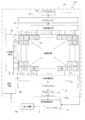
- FIG. 1 schematically shows an exemplary configuration of an imaging device according to a first embodiment of the present disclosure.
- Each of the image pickup apparatus 100A shown in FIG. 1 includes a plurality of pixels Px having a photoelectric conversion unit supported by the semiconductor substrate 110 as a part thereof. That is, in the following, as the image pickup device 100A, an image pickup device having a so-called stacked structure will be illustrated.
- the semiconductor substrate 110 has a plurality of readout circuits formed corresponding to each pixel Px.
- the plurality of pixels Px are arranged two-dimensionally on the semiconductor substrate 110 to form an imaging region.
- the plurality of pixels Px are arranged in a plurality of rows and columns.
- a plurality of pixels Px are arranged in m rows and n columns.
- m and n independently represent an integer of 2 or more.
- the image pickup apparatus 100A has a plurality of line signal lines Ri and a plurality of output signal lines.
- the plurality of line signal lines R i include m line signal lines R 0 , R 1 , R 2 , ..., R m-2 , R m-1 arranged corresponding to a plurality of lines of the pixel Px. ..
- Each of the plurality of row signal lines R i is electrically connected to one or more pixels Px of the same row.
- These row signal lines R i is connected to the row scanning circuit 130.
- the plurality of output signal lines include a plurality of first output signal lines S j and a plurality of second output signal lines T j .
- the plurality of first output signal line S j, the first output signal line S 0 of the n arranged corresponding to the plurality of columns of pixels Px, S 1, S 2, ..., S n-2, S n -1 is included.
- the plurality of second output signal lines T j also have n second output signal lines T 0 , T 1 , T 2 , ..., T n-2 arranged corresponding to the plurality of rows of pixels Px. , T n-1 .
- Each of the plurality of first output signal lines Sj is electrically connected to a read circuit of one or more pixels Px belonging to the same row.
- the first analog-digital conversion circuit 141 and the first digital output interface 161 are connected to the plurality of first output signal lines Sj . From the first digital output interface 161, a signal read from the pixel Px via the first output signal line Sj and subjected to analog-to-digital conversion by the first analog-to-digital conversion circuit 141 is output.
- each of the plurality of second output signal line T j is electrically connected to the readout circuit of one or more pixels Px belonging to the same column.
- Each second output signal line T j is connected to, for example, a plurality of pixels belonging to the same row other than the pixels connected to the first output signal line S j .
- a second analog-to-digital conversion circuit 142 and a second digital output interface 162 are connected to the plurality of second output signal lines Tj . From the second digital output interface 162, via the second output signal line T j read from the pixel Px, second analog - signal subjected to the digital conversion is output - analog by the digital conversion circuit 142.
- the analog-to-digital conversion circuit is simply referred to as the "AD conversion circuit” and the digital output interface is simply referred to as the "interface" below.
- the image pickup apparatus 100A further includes a first digital memory 151 connected between the first AD conversion circuit 141 connected to the first output signal line Sj and the first interface 161.
- the image pickup apparatus 100A also has a second digital memory 152 which is connected between the first 2AD conversion circuit 142 connected to the second output signal line T j and the second interface 162.
- the first digital memory 151 and the second digital memory 152 temporarily transmit one line of digital signals read from a plurality of pixels Px and analog-digitally converted by the first AD conversion circuit 141 or the second AD conversion circuit 142. Hold.
- the result of one line of analog-digital conversion is held in the digital memory, and the AD conversion circuit is used for the analog-related to the next line. It will be possible to perform digital conversion. That is, line-by-line analog-to-digital conversion can be processed at higher speed.
- An image processing circuit 170A is connected to the first interface 161 and the second interface 162.
- the image processing circuit 170A executes processing such as gamma correction, color interpolation processing, spatial interpolation processing, and auto white balance on the digital signal output from the interface, if necessary.
- the image processing circuit 170A can be realized by, for example, a DSP (Digital Signal Processor), an ISP (Image Signal Processor), an FPGA (field-programmable gate array), or the like.
- control circuit 220 is electrically connected to the image processing circuit 170A.
- the image processing circuit 170A provides the control circuit 220 with control signals such as a vertical synchronization signal and a horizontal synchronization signal.
- a row scanning circuit 130, a first AD conversion circuit 141, and a second AD conversion circuit 142 are connected to the control circuit 220.
- the control circuit 220 is implemented by, for example, a microcontroller including one or more processors and typically has a timing generator.
- the control circuit 220 supplies a drive signal to the row scanning circuit 130, the first AD conversion circuit 141, and the second AD conversion circuit 142, and controls the entire image pickup apparatus 100A.
- the arrow extending toward the control circuit 220 and the arrow extending from the control circuit 220 schematically represent an input signal to the control circuit 220 and an output signal from the control circuit 220, respectively.
- the control circuit 220 may include one or more memories.
- the image pickup device 100A may include a display device 180 such as a liquid crystal display or an organic EL display connected to the image processing circuit 170A.
- the display device 180 presents an image based on the digital signal obtained by photographing to the user of the image pickup device 100A.
- the image processing circuit 170A has a first frame memory 171.
- the first frame memory 171 temporarily holds digital data corresponding to one frame of images output from the first interface 161 and / or the second interface 162.
- the first frame memory 171 temporarily holds the first digital signal corresponding to the reset signal expressing the reset level.
- the first digital signal is a digital signal output from the first AD conversion circuit 141 or the second AD conversion circuit 142 by inputting a reset signal which is an analog signal read from each pixel Px.
- the image processing circuit 170A outputs the difference between the first digital signal held in the first frame memory 171 and the second digital signal corresponding to the pixel signal expressing the image of the subject.
- the difference between the digital signals can substantially cancel the effect of random noise due to the reset operation performed immediately before the exposure period.
- the image pickup apparatus 100A includes a first system including the first output signal line S j and a second system including the second output signal line T j with respect to reading a signal from the pixels. It has two systems of.
- the first output signal line Sj is connected to one or more pixels in that row.
- the second output signal line Tj is connected to one or more other pixels in the row.
- the reset signal is read from a certain pixel and the pixel signal is read from a pixel belonging to a row different from the row to which the pixel belongs. Can be executed in parallel. Therefore, since the interval between the read period of the reset signal line by line and the read period of the pixel signal line can be reduced, it is possible to improve the frame rate while removing the influence of the reset noise. ..
- FIG. 2 shows an exemplary circuit configuration of the image pickup apparatus 100A.
- four pixels Px included in the imaging region shown in FIG. 1 are taken out and schematically shown.
- These four pixels Px include a first pixel Px1, a second pixel Px2, a third pixel Px3, and a fourth pixel Px4 arranged in 2 rows and 2 columns.
- the first pixel Px1 and the second pixel Px2 are located in the same row, while the third pixel Px3 and the fourth pixel Px4 are in the same row different from the first pixel Px1 and the second pixel Px2. Located in.
- the first pixel Px1 and the second pixel Px2 are located in, for example, even rows of a pixel array containing a plurality of pixels Px, and the third pixel Px3 and the fourth pixel Px4 are located in odd rows of the pixel array.
- the basic circuit configuration of the pixels is common among these pixels Px1 to Px4, and therefore, an exemplary configuration of each pixel will be described below with a focus on the first pixel Px1.
- the first pixel Px1 includes a photoelectric conversion unit 10 and a readout circuit 20 electrically connected to the photoelectric conversion unit 10.
- the photoelectric conversion unit 10 has a pixel electrode, a counter electrode, and a photoelectric conversion layer sandwiched between these electrodes.
- the photoelectric conversion unit 10 of each pixel has an electrical connection with a voltage line 192 connected to the voltage supply circuit 190, and a predetermined voltage is applied between the pixel electrode and the counter electrode during the operation of the image pickup apparatus 100A. It is configured to be possible.
- the voltage supply circuit 190 may be configured so that a predetermined voltage can be applied to the photoelectric conversion unit 10 of each pixel when the image pickup apparatus 100A operates, and is not limited to a specific power supply circuit.
- the voltage supply circuit 190 may be a circuit that generates a predetermined voltage, or may be a circuit that converts a voltage supplied from another power source into a predetermined voltage.
- the voltage supply circuit 190 may be a part of the row scanning circuit 130.
- the read circuit 20 includes a signal detection transistor 22, an address transistor 24, and a reset transistor 26.
- the signal detection transistor 22, the address transistor 24, and the reset transistor 26 are typically field effect transistors formed on the semiconductor substrate 110, and an example in which an N-channel MOSFET is used for these transistors will be described below.
- the gate of the signal detection transistor 22 is connected to the pixel electrode of the photoelectric conversion unit 10.
- the source of the signal detection transistor 22 is connected to the corresponding output signal line via the address transistor 24.
- a set of a first output signal line Sj and a second output signal line Tj is arranged for each of a plurality of columns of the plurality of pixels Px.
- the first output signal line Sj is connected to the first AD conversion circuit 141.
- the second output signal line T j is connected to the 2AD conversion circuit 142.
- the source of the signal detection transistor 22 of the first pixel Px1 is electrically connected to the first output signal line Sj . Is connected.
- the source of the signal detection transistor 22 of the fourth pixel Px4 is electrically connected to the second output signal line Tj .
- the source of the signal detection transistor 22 of the second pixel Px2 is electrically connected to the first output signal line S j-1.
- the source of the signal detection transistor 22 of the third pixel Px3 is electrically connected to the second output signal line Tj -1 . That is, in this example, the first AD conversion circuit 141 generates a digital signal corresponding to the analog signal read from, for example, the first pixel Px1 and the second pixel Px2 located in the even rows of the pixel array by analog-digital conversion. , Output to the first interface 161. Further, the second AD conversion circuit 142 generates a digital signal corresponding to an analog signal read from, for example, the third pixel Px3 and the fourth pixel Px4 located in the odd-numbered rows of the pixel array, and outputs the digital signal to the second interface 162.
- the analog signal read from each pixel Px includes a reset signal expressing the reset level and a pixel signal expressing the image of the subject.
- the reset signal and the pixel signal read from each pixel Px are signals on which kTC noise generated by resetting the pixels is superimposed.
- the first AD conversion circuit 141 and the second AD conversion circuit 142 may have a plurality of elements provided for each output signal line, such as a column signal processing circuit 145. Each of these plurality of elements is connected to the corresponding one of the plurality of output signal lines.
- the drain of the signal detection transistor 22 of each pixel is connected to the power supply line 194.
- the power supply line 194 functions as a source follower power supply by applying a power supply voltage VDD of about 3.3 V during operation of the image pickup apparatus 100A.
- a line signal line Ri is connected to the gate of the address transistor 24.
- Row scanning circuit 130 is controlled by the voltage level applied to the row signal lines R i, it switches on and off of the address transistor 24. As a result, the row scanning circuit 130 can read a signal from the pixels belonging to the selected row to the corresponding output signal line.
- the readout circuit 20 includes a reset transistor 26.
- One of the drain and source of the reset transistor 26 is connected to a node FD that electrically connects the photoelectric conversion unit 10 to the gate of the signal detection transistor 22.
- the other of the drain and source of the reset transistor 26 is connected to the reset voltage line 196.
- the reset voltage line 196 is connected to the reset voltage supply circuit 198.
- a predetermined reset voltage VRST is applied from the reset voltage supply circuit 198 to the reset voltage line 196.
- the reset voltage VRST for example, a voltage of 0V or a voltage near 0V is used.
- the reset voltage supply circuit 198 may be configured so that a predetermined reset voltage can be applied to each pixel during the operation of the image pickup apparatus 100A, and is not limited to a specific power supply circuit like the voltage supply circuit 190.
- the reset voltage supply circuit 198 may be a circuit independent of the voltage supply circuit 190, and one of the reset voltage supply circuit 198 and the voltage supply circuit 190 may be a part of the other.
- a plurality of reset signal line Q i are provided corresponding to the plurality of pixels Px. As shown, typically, one reset signal line is commonly connected to the gates of the reset transistors 26 of a plurality of pixels Px belonging to the same row. In this example, the reset signal line Q i has a connection to the row scanning circuit 130.
- the row scanning circuit 130 is controlled by the voltage level applied to the reset signal line Q i, by turning on the reset transistor 26 in a row unit of a plurality of pixels Px, nodes pixel Px reset transistor 26 is turned on The potential of the FD can be reset to VRST .
- FIG. 3 schematically shows the device structure of the first pixel Px1.
- the first pixel Px1 generally includes a semiconductor substrate 110 on which a readout circuit 20 is formed, and a photoelectric conversion unit 10 supported by the semiconductor substrate 110. As shown in FIG. 3, typically, an insulating layer 50 covering the readout circuit 20 is arranged between the semiconductor substrate 110 and the photoelectric conversion unit 10.
- the photoelectric conversion unit 10 includes a pixel electrode 11 supported by the insulating layer 50, a translucent counter electrode 13, and a photoelectric conversion layer 12 located between the pixel electrode 11 and the counter electrode 13.
- the pixel electrode 11 is located closer to the semiconductor substrate 110 than the photoelectric conversion layer 12, and is made of a metal such as aluminum or copper, a metal nitride, or polysilicon that has been imparted with conductivity by being doped with impurities. Can be formed.
- the pixel electrode 11 is electrically separated from the pixel electrodes 11 of other adjacent pixels by being spatially separated from the pixel electrodes 11.
- the counter electrode 13 is located on the side where the light from the subject arrives.
- the counter electrode 13 is a translucent electrode formed of a conductive material such as ITO.
- the term "translucency" in the present specification means that the photoelectric conversion layer 12 transmits at least a part of light having a wavelength that can be absorbed, and transmits light over the entire wavelength range of visible light. Is not required.
- An optical filter such as a color filter, a microlens, or the like may be arranged on the main surface of the counter electrode 13 on the side opposite to the photoelectric conversion layer 12.
- the counter electrode 13 is typically provided in the form of a single continuous electrode layer straddling a plurality of pixels.
- the voltage line 192 described above is connected to the counter electrode 13 of the photoelectric conversion unit 10.
- the voltage line 192 is shown to be connected to each photoelectric conversion unit 10 of a plurality of pixels, but typically, the counter electrode 13 of each pixel is continuous between the plurality of pixels. It is part of a single translucent electrode. Therefore, the counter electrode 13 of each pixel is basically equipotential, and it is not essential that the voltage line 192 is a wiring branched into a plurality of lines.
- the photoelectric conversion layer 12 is formed of an organic material or an inorganic material such as amorphous silicon, and receives light incident through the counter electrode 13 to generate a charge pair. Like the counter electrode 13, the photoelectric conversion layer 12 is typically provided in the form of a single photoelectric conversion structure that is continuous across a plurality of pixels. That is, the photoelectric conversion layer 12 in each pixel can be a part of the photoelectric conversion layer continuously formed over a plurality of pixels.
- the photoelectric conversion layer 12 By forming the photoelectric conversion layer 12 by selecting one or more suitable materials as the photoelectric conversion material, for example, it is possible to obtain the photoelectric conversion layer 12 exhibiting sensitivity in both the visible region and the infrared region. .. Examples of such materials are described in detail in, for example, WO 2018/025544. For reference, the entire disclosure of International Publication No. 2018/025544 is incorporated herein by reference.
- the photoelectric conversion layer 12 may be composed of quantum dots and / or nanotubes. Alternatively, the photoelectric conversion layer 12 may include quantum dots and / or nanotubes as the photoelectric conversion material.
- the photoelectric conversion layer 12 may include a layer made of an organic material and a layer made of an inorganic material.
- the insulating layer 50 located between the semiconductor substrate 110 and the photoelectric conversion unit 10 includes, for example, a plurality of insulating layers each formed of silicon dioxide. As schematically shown in FIG. 3, a multilayer wiring including at least a conductive structure 52 having one end connected to a pixel electrode 11 of a photoelectric conversion unit 10 is provided inside the insulating layer 50.
- the conductive structure 52 may include vias and wiring made of metal such as copper, plugs made of polysilicon, and the like. In the illustrated example, the other end of the conductive structure 52 is electrically connected to the impurity region 111 formed on the semiconductor substrate 110.
- the semiconductor substrate 110 has impurity regions 112, 113, 114 and 115 in addition to the impurity regions 111.
- the semiconductor substrate 110 also has an element separation region 116 that electrically separates the readout circuit 20 provided for each pixel Px between the pixels Px.
- a P-type silicon substrate will be illustrated as the semiconductor substrate 110.
- the semiconductor substrate 110 may be an insulating substrate or the like having a semiconductor layer provided on its surface.
- Each of the impurity regions 111, 112, 113, 114 and 115 is typically an N-type diffusion region.
- the impurity region 111 to which the conductive structure 52 is connected functions as one of the source region and the drain region of the reset transistor 26.
- the reset transistor 26 further includes an impurity region 112 that functions as the other of the source region and the drain region, a gate insulating layer 26 g on the semiconductor substrate 110, and a gate electrode 26e on the gate insulating layer 26 g.
- the reset voltage line 196 described above is connected to the impurity region 112.
- the signal detection transistor 22 includes an impurity region 113 and an impurity region 114, a gate insulating layer 22 g on the semiconductor substrate 110, and a gate electrode 22e on the gate insulating layer 22 g.
- the impurity region 113 functions as a drain region of the signal detection transistor 22, and the impurity region 114 functions as a source region of the signal detection transistor 22.
- the power line 194 described above is connected to the impurity region 113.
- the element separation region 116 is also provided between the signal detection transistor 22 and the reset transistor 26.
- the address transistor 24 includes an impurity region 114 and an impurity region 115, a gate insulating layer 24 g on the semiconductor substrate 110, and a gate electrode 24e on the gate insulating layer 24 g.
- the impurity region 114 and the impurity region 115 function as a drain region and a source region of the address transistor 24, respectively.
- the address transistor 24 shares the impurity region 114 with the signal detection transistor 22.
- the corresponding one of the plurality of output signal lines S j and T j described above is connected to the impurity region 115.
- the insulating layer 50 covers the signal detection transistor 22, the address transistor 24, and the reset transistor 26.
- the conductive structure 52 in the insulating layer 50 also has an electrical connection with the gate electrode 22e of the signal detection transistor 22. That is, the conductive structure 52 in each pixel has a function of electrically connecting the pixel electrode 11 of the photoelectric conversion unit 10 and the readout circuit 20 including the signal detection transistor 22 formed on the semiconductor substrate 110 to each other.
- the conductive structure 52 also has a function as a part of a charge storage region for temporarily storing the electric charge collected by the pixel electrode 11, that is, the signal charge.
- the voltage supply circuit 190 applies a predetermined voltage to the photoelectric conversion unit 10 of each pixel via the voltage line 192.
- a predetermined potential difference ⁇ V can be applied between the counter electrode 13 and the pixel electrode 11 during the exposure period.
- a voltage to the counter electrode 13 so that the potential of the counter electrode 13 is higher than that of the pixel electrode 11 with the pixel electrode 11 as a reference, positive light is generated in the photoelectric conversion layer 12 by the incident light.
- a charge having a positive polarity for example, a hole can be collected by the pixel electrode 11 as a signal charge.
- the signal charge is temporarily stored in the charge storage region including the conductive structure 52 as a part thereof.
- the impurity region 111 formed on the semiconductor substrate 110, the pixel electrode 11 of the photoelectric conversion unit 10, and the gate electrode 22e of the signal detection transistor 22 also have a charge storage region that temporarily stores signal charges. Acts as part of.
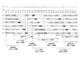
- Example driving method of image pickup apparatus 100A 4 and 5 are diagrams for explaining an example of a method of driving the image pickup apparatus according to the first embodiment of the present disclosure.
- the top chart shows the pulse of the vertical sync signal VD.
- the rising edge of the pulse of the vertical sync signal VD represents the start of a period for reading the pixel signal.
- the second chart from the top in FIG. 4 shows the pulse of the horizontal synchronization signal HD.
- the period from the rise of one pulse to the rise of the next pulse corresponds to one horizontal scanning period of 1H.
- FIG. 4 a plurality of blocks showing the operation of the plurality of pixels Px included in the imaging region are also shown in one figure.
- the number of rows of the plurality of pixel Px is 6 rows of the 0th row R 0 to the 5th row R 5
- the operation of the pixel Px is schematically shown by a plurality of rectangular blocks.
- Row 0 R 0 of a plurality of pixels Px includes, for example, a first pixel Px1 and the second pixel Px2 described above
- the first row R 1 includes, for example, a third pixel Px3 and the fourth pixel Px4 above.
- the white rectangular block schematically represents the exposure period of the frame period
- the rectangular block hatched by vertical lines is the reading of the reset level corresponding to the signal level in the dark. Represents a period.
- the rectangular block with hatching by diagonal lines represents the period for reading the pixel signal representing the image of the subject.
- the driving method of the image pickup apparatus illustrated in FIG. 5 is roughly a step of resetting the potential of the charge storage region of the pixel (step S1) and a reset according to the potential of the charge storage region after resetting the pixel.
- a step of reading a signal step S2
- a step of generating a first digital signal corresponding to a reset signal by analog-digital conversion step S3
- a step of storing the first digital signal in a frame memory step S4.
- step S6 A step of reading a signal (step S6), a step of generating a second digital signal corresponding to a pixel signal by analog-digital conversion (step S7), and a step of obtaining a difference between the second digital signal and the first digital signal (step S7).
- step S8 A step of reading a signal (step S6), a step of generating a second digital signal corresponding to a pixel signal by analog-digital conversion (step S7), and a step of obtaining a difference between the second digital signal and the first digital signal (step S7).
- step S8 details of an exemplary driving method of the imaging device will be described with reference to FIG.
- FIG. 4 shows an example of an operation based on a so-called rolling shutter, which executes exposure and signal reading for each row of a plurality of pixels.
- first attention is paid to the 0th row R 0 of row 0 R 0 ⁇ fifth row R 5.
- the charge storage area of each pixel Px is reset.
- k is an integer of 0 or more
- the reset of a plurality of pixels belonging to the 0th row R0 is started at time t3 with respect to the kth frame period.
- the signal detection transistor 22 of the readout circuit 20 has a pixel electrode 11 due to the gate electrode 22e being electrically connected to the pixel electrode 11 via the conductive structure 52. Outputs a signal according to the potential. That is, the readout circuit 20 outputs an analog signal corresponding to the potential of the pixel electrode 11 by the source follower including the signal detection transistor 22.
- ⁇ Process of reading the reset signal> After turning off the reset transistor 26, by turning on the address transistor 24, a signal corresponding to a reset voltage V RST applied to the gate electrode 22e of the signal detection transistor 22 is output to the corresponding output signal line ..
- the signal output to the output signal line at this time is an analog signal expressing the reset level, and usually includes reset noise generated when the reset transistor 26 is turned off.
- the reset signal read from the pixel belonging to the 0th line R0 is passed through the corresponding one of the first output signal lines Sj. It is input to the first AD conversion circuit 141.
- the reset signal input to the first AD conversion circuit 141 is converted into a digital signal by the first AD conversion circuit 141.
- the address transistor 24 is turned off.
- the reading of the reset signal from the pixel belonging to the 0th row R0 is completed.
- the above-mentioned reading operation is sequentially executed line by line in synchronization with the horizontal synchronization signal HD.
- the pulse interval of the horizontal synchronization signal HD that is, the 1H period represents the period from the selection of one line to the selection of the next line.
- the pixel belonging to the 0th row R0 is reset and the reset signal is read from the pixel during the period from time t3 to time t4, and the first is executed during the period from time t4 to time t5. running a read reset signal from the reset and the pixels of the pixel belonging to row R 1.
- the reset level read period may include a reset period for resetting the potential in the charge storage region of the pixel.
- the reset signals read from the pixels belonging to the first row R 1 is the first output signal line S j without the second output signal line T It is input to the second AD conversion circuit 142 via the corresponding one of j . That is, here, the reset signal read from the pixels located in the even-numbered rows and the reset signal read from the pixels located in the odd-numbered rows are passed through different output signal lines to the first AD conversion circuit 141. And is input to any of the second AD conversion circuits 142. The reset signal input to the second AD conversion circuit 142 is also converted into a digital signal by analog-digital conversion.
- the digital signals output from the first AD conversion circuit 141 and the second AD conversion circuit 142 are input to the image processing circuit 170A via the first interface 161 and the second interface 162, respectively.
- the first digital signal corresponding to the reset signal read between the time t3 and the time t9 in FIG. 4 is temporarily held in the first frame memory 171 in the image processing circuit 170A.
- the reset transistor 26 After reading the reset signal, the reset transistor 26 is turned off and the exposure period is started.
- the period from the time t4 to the time t8 is the exposure period in the kth frame period.
- the exposure period is a period for accumulating the signal charge generated by the photoelectric conversion unit 10 according to the exposure amount to the pixel in the charge storage region.
- the length of the exposure period of each row of the plurality of pixels Px is, for example, in the range of 1/60 seconds to 1/16000 seconds.
- the counter electrode 13 of the photoelectric conversion unit 10 of each pixel Px receives a predetermined voltage V1 from the voltage supply circuit 190 via the voltage line 192, so that the pixel electrode 11 is in a high potential state, for example. It is said that.
- the potential of the pixel electrode 11 immediately after the reset is determined by the above-mentioned reset voltage VRST , and immediately after the reset, a bias voltage of (V1-V RST ) is applied between the pixel electrode 11 and the counter electrode 13. is there.
- the positive charge of the charge pairs generated by the photoelectric conversion is collected by the pixel electrode 11.
- the PN junction formed in the semiconductor substrate 110 by forming the impurity region 111 functions as a junction capacitance for temporarily accumulating the positive charges collected by the pixel electrodes 11.
- the potential of the impurity region 111 as the charge storage portion rises as the signal charge accumulates in the impurity region 111.
- (V1-V RST )>0 but for example, a voltage is applied to the counter electrode 13 so that the potential of the counter electrode 13 is lower than that of the pixel electrode 11. Therefore, for example, it is also possible to use electrons as signal charges.
- the pixel signal is read out.
- the reading of the signal from the pixel belonging to the 0th row R0 is started at time t8 based on the vertical synchronization signal VD.
- the read-out circuit 20 of each pixel belonging to the 0th row R0 outputs an analog signal corresponding to the potential of the pixel electrode 11 to the corresponding one of the plurality of first output signal lines.
- Signal read from the pixel of row 0 R 0 at this time is an analog signal corresponding to the charge amount accumulated in the charge accumulation region in the exposure period for the 0th row R 0, based on ambient light such as sunlight It is a pixel signal that expresses an image of a subject. This pixel signal contains reset noise caused by a reset operation performed before the exposure period. After reading the pixel signal, the address transistor 24 is turned off again.
- the pixel signal read from the pixels of the 0th line R 0 , the 2nd line R 2 and the 4th line R 4 is the first output signal line S j . It is sent to the 1AD conversion circuit 141.
- the first row R 1, the third row R 3, pixel signals read from the pixels of the fifth row R 5 is sent to the 2AD conversion circuit 142 via the second output signal line T j.
- the first AD conversion circuit 141 and the second AD conversion circuit 142 perform analog-digital conversion on a line-by-line basis for the received pixel signal, and generate a second digital signal corresponding to the pixel signal.
- the generated second digital signal is sent to the image processing circuit 170A via the first interface 161 or the second interface 162.
- the image processing circuit 170A calculates the difference between the second digital signal corresponding to the pixel signal and the first digital signal corresponding to the reset signal, and outputs this difference as pixel value data.
- the reset signal read from the pixel after resetting the potential in the charge storage region is superposed with the reset noise generated by the reset. Further, the reset signal is read in a non-destructive manner, and the potential of the charge storage region is not reset again in the period until the pixel signal is read. Therefore, the pixel signal corresponding to the amount of charge accumulated in the charge accumulation region during the exposure period is also in a state in which reset noise is superimposed.
- the difference between these digital signals is obtained. Therefore, by subtracting the first digital signal corresponding to the reset signal, the reset noise is substantially subtracted from the second digital signal corresponding to the pixel signal, and as a result, the influence of the reset noise is effectively canceled. To.
- FIG. 4 is a schematic of the 1H period from the time t8 shown in FIG. 4 to time t9, the operation of the readout circuit 20 of the 0th row pixel of R 0, and the operation of the readout circuit of a pixel in the fifth row R 5 Shown in.
- FIG. 4 is a schematic of the 1H period from the time t8 shown in FIG. 4 to time t9, the operation of the readout circuit 20 of the 0th row pixel of R 0, and the operation of the readout circuit of a pixel in the fifth row R 5 Shown in.
- the graph of ⁇ S represents the waveform of the address control signal applied to the gate of the address transistor 24 of the read circuit 20, and the graph of ⁇ R is applied to the gate of the reset transistor 26 of the read circuit 20. It represents the waveform of the reset control signal.
- the graph of V 0 schematically shows the period during which the signal read from the pixel of row 0 R 0 is analog-digitally converted by the first AD conversion circuit 141. In other words, it represents the output waveform from the first AD conversion circuit 141.
- the graph of V 5 schematically shows the period during which the signal read from the pixel of row 5 R 5 is analog-digitally converted by the second AD conversion circuit 142. In other words, it represents the output waveform from the second AD conversion circuit 142.
- the timing of the output of the second digital signal corresponding to the pixel signal is the same.
- the result of one line of analog-digital conversion of the plurality of pixels Px may be output at a common timing between the first AD conversion circuit 141 and the second AD conversion circuit 142.
- the output of the result of the analog-to-digital conversion matches between the first AD conversion circuit 141 and the second AD conversion circuit 142.
- FIG. 7 schematically shows the operation of the readout circuit 20 with respect to the pixels in the hth row and the kth row, which are different from each other in the pixel array.
- a first output signal line and a second output signal line are provided for each row of a plurality of pixels Px, and a part of the plurality of pixels Px is used.
- reading of the reset signal from one pixel and reading of the pixel signal from another pixel are executed in parallel. Will be possible.
- a part of the reset signal read period and the pixel signal read are performed. It becomes possible to overlap a part of the period, and the length of the exposure period can be flexibly changed. For example, the exposure period can be shortened to improve the frame rate.
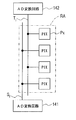
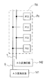
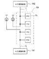
- the 2AD conversion circuit 142 is separated and arranged.
- the arrangement of the first AD conversion circuit 141 and the second AD conversion circuit 142 is not limited to this example.
- the first AD conversion circuit 141 and the second AD conversion circuit 142 may be arranged in the vicinity of one side of the imaging region RA having a substantially rectangular shape.
- first AD conversion circuit 141 and the second AD conversion circuit 142 need not be formed on the semiconductor substrate 110 provided with the plurality of pixels Px.
- a first AD conversion circuit 141, a second AD conversion circuit 142, a first digital memory 151, a second digital memory 152, and an image processing circuit are placed on another circuit board 120 different from the semiconductor board 110.
- a configuration such as arranging 170A or the like is also possible.
- the pixels located in the even-numbered rows and the pixels located in the odd-numbered rows of the plurality of pixels Px are connected to the first output signal line Sj and the second output signal line Tj , respectively.
- the connection of the pixels to the first output signal line S j and the second output signal line T j is not limited to these modes.
- 11 and 12 schematically show other examples of pixel connections to output signal lines. Configuration shown in FIG. 11 is an example of connecting alternately the pixels in every two rows of a plurality of pixels Px to the first output signal line S j and the second output signal line T j.
- FIG. 12 shows four output signal lines, a first output signal line S j , a second output signal line T j , a third output signal line U j, and a fourth output signal line V j , for each row of a plurality of pixels Px.
- the first output signal line S j , the second output signal line T j , the third output signal line U j, and the fourth output signal line V j are combined with the first AD conversion circuit 141 and the second AD conversion circuit 142.
- the third AD conversion circuit 143 and the fourth AD conversion circuit 144 are connected, respectively.
- a part of the plurality of pixels Px is connected to the first output signal line Sj connected to the first AD conversion circuit 141, and the other part is connected to the first output signal line Sj . It may be connected to the second output signal line T j that is connected to the 2AD conversion circuit 142.
- the imaging region RA is divided into two regions, and the pixel connection destination is either the first AD conversion circuit 141 or the second AD conversion circuit 142 depending on which region it belongs to. You may decide.
- the imaging region RA is divided into two regions, upper and lower.
- the pixels located in the lower half region of the imaging region RA are connected to the first output signal line Sj connected to the first AD conversion circuit 141.
- pixels positioned in the upper half region of the imaging region RA is connected to the second output signal line T j that is connected to the 2AD conversion circuit 142.
- Pixel signal reading can be performed line by line. That is, the overlap between the read-out period of the reset signal for some pixels and the read-out period of the pixel signal for some other pixels is allowed, and for example, the effect of shortening the frame rate can be obtained.
- the first AD conversion circuit 141 and the second AD conversion circuit 142 corresponds to the reset signal read from that pixel. Both the first digital signal to be generated and the second digital signal corresponding to the pixel signal are generated. However, as described below, the first AD conversion circuit converts the digital signal corresponding to the analog signal read from the pixel into a digital signal depending on whether the analog signal read from the pixel is a reset signal or a pixel signal. You may switch whether to output from 141 or the second AD conversion circuit 142.
- FIG. 14 shows a modified example of the image pickup apparatus according to the first embodiment of the present disclosure.
- a first AD conversion circuit 141 In order to avoid the drawing from becoming excessively complicated, in FIG. 14, four pixels belonging to a certain row are taken out and shown among a plurality of pixels Px, and in FIG. 14, an image processing circuit is shown.
- the illustration of elements common to the image pickup apparatus 100A, such as 170A, is omitted.
- the first signal A switching circuit 31 is interposed between the first output signal line S j and the second output signal line T j corresponding to the column that belongs the pixel.
- the first signal switching circuit 31 may be a part of each pixel.
- the pixel is the first output signal line Sj , depending on whether the analog signal read from the pixel is a reset signal or a pixel signal. And which of the second output signal line Tj is connected is switched. For example, when the output from the pixel read circuit 20 is a reset signal, the first signal switching circuit 31 establishes a connection between the pixel read circuit 20 and the first output signal line Sj, and the pixel When the output from the reading circuit 20 of the above is a pixel signal, the connection between the reading circuit 20 of the pixel and the second output signal line Tj is established.
- the first signal switching circuit 31 can be realized in the form of a circuit including a switching element such as a field effect transistor formed on the semiconductor substrate 110, for example. These switching elements are operated in synchronization with the pixel reading circuit 20 based on, for example, the drive signal Ds from the control circuit 220. As a result, the first signal switching circuit 31 establishes a connection between the read circuit 20 and the first output signal line Sj when the reset signal is output from the read circuit 20, and the pixel signal from the read circuit 20 is input. At the time of output, the connection between the read circuit 20 and the second output signal line Tj can be established.
- the 1AD conversion circuit 141 connected to the first output signal line S j is an analog reset signal read from each pixel - responsible for digital conversion, the second output signal line T j
- the connected second AD conversion circuit 142 is responsible for analog-to-digital conversion of the pixel signal read from each pixel.
- the AD conversion circuit that outputs the first digital signal and the AD conversion circuit that outputs the second digital signal may be provided in the image pickup apparatus. Even with such a configuration, it is possible to read a pixel signal from a pixel in another row in parallel with reading a reset signal from a pixel in a certain row in the imaging region RA.
- the period for reading the reset signal and the period for reading the pixel signal can be overlapped, and the frame rate can be flexibly changed. Further, by calculating the difference between the first digital signal held in the first frame memory 171 and the second digital signal corresponding to the first digital signal by the image processing circuit 170A, it is mixed in these signals. The reset noise that has been generated can be effectively canceled. As described with reference to FIGS. 6 and 7, the timing of the output of the first digital signal from the first AD conversion circuit 141 and the timing of the output of the second digital signal from the second AD conversion circuit 142 are , May match or may be out of alignment.
- FIG. 15 shows another modification of the imaging device according to the first embodiment of the present disclosure.
- the image pickup apparatus 100C shown in FIG. 15 some of the pixels belonging to the same row in the imaging region RA are connected to the first output signal line Sj . It is connected and the remaining pixels are connected to the second output signal line Tj .
- the first signal switching circuit 31 is not disposed.
- the first signal switching circuit 33 is connected between the set of the first output signal line S j and the second output signal line T j and the first AD conversion circuit 141, and the first output signal line S j is also connected. and the second signal switching circuit 34 is connected between the second output signal line T j of the set and the 2AD conversion circuit 142.
- the first signal switching circuit 33 and the second signal switching circuit 34 switch the connection of the output signal line between the AD conversion circuit and the source follower power supply, for example, based on the drive signal Dt from the control circuit 220.
- each of the first signal switching circuit 33 and the second signal switching circuit 34 may be configured to operate in the same manner as the four-way switch. However, these operations are complementary between the first signal switching circuit 33 and the second signal switching circuit 34.
- “the first signal switching circuit 33 and the second signal switching circuit 34 operate complementarily” means that one of the first signal switching circuit 33 and the second signal switching circuit 34 operates the first output signal line Sj.
- the other of the first signal switching circuit 33 and the second signal switching circuit 34 connects the output signal line and the source follower power supply. It means establishing a connection between them.
- the first signal switching circuit 33 establishes a connection between the first output signal line Sj and the first AD conversion circuit 141
- the second signal switching circuit 34 has the first output signal line Sj and the source follower power supply. Establish a connection with.
- the first signal switching circuit 33 is in a state of establishing the connection between the second output signal line Tj and the source follower power supply, and the second signal switching circuit 34 is in the second output signal line T.
- the connection between j and the second AD conversion circuit 142 has been established.
- the first AD conversion circuit 141 when the first AD conversion circuit 141 is connected to the first pixel via the first output signal line Sj to perform analog-to-digital conversion of the reset signal output from the first pixel, for example, the first 2AD conversion circuit 142, by being connected to the second pixel with the other via the second output signal line T j, analog pixel signals output from the second pixel - concurrently executing digital conversion.
- the connections in the first signal switching circuit 33 and the second signal switching circuit 34 are switched as schematically shown by the dotted lines in FIG.
- the 1AD conversion circuit 141 an analog of the output reset signal from the second pixel by being connected to the second pixel through the second output signal line T j - can perform digital conversion,
- the second AD conversion circuit 142 By connecting the second AD conversion circuit 142 to the first pixel via the first output signal line Sj , the analog-to-digital conversion of the pixel signal output from the first pixel can be executed in parallel. ..
- one of the first AD conversion circuit 141 and the second AD conversion circuit 142 is responsible for analog-to-digital conversion of the reset signal read from each pixel, and the first AD conversion circuit 141 and the second AD conversion.
- the other side of the circuit 142 is responsible for analog-to-digital conversion of the pixel signal read from each pixel.
- the pixels located in the even-numbered lines of the imaging region RA are connected to the first output signal line Sj
- the pixels located in the odd-numbered lines of the imaging region RA are connected to the second output signal line Tj . You are connected.
- connection of pixels to the output signal line is not limited to this example, and a part of the plurality of pixels Px is connected to the first output signal line S j , and the remaining pixels are connected to the second output signal line T j. It suffices if it is connected to.
- FIG. 16 schematically shows an exemplary configuration of an imaging device according to a second embodiment of the present disclosure.
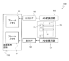
- the image pickup apparatus 100D shown in FIG. 16 has an image processing circuit 170B instead of the image processing circuit 170A.
- the image processing circuit 170B has a second frame memory 172 in addition to the first frame memory 171.
- the first frame memory 171 temporarily holds the first digital signal generated from the reset signal expressing the reset level
- the second frame memory 172 is, for example, from the pixel signal expressing the image of the subject. Temporarily hold the generated second digital signal.
- the image processing circuit 170B calculates the difference between the second digital signal held in the second frame memory 172 and corresponding to the image data of one frame and the first digital signal held in the first frame memory 171. And output.
- a second frame memory 172 that temporarily holds a second digital signal for one frame in the image pickup apparatus in addition to the first frame memory 171, for example, pixels acquired in the next frame period. It is also possible to obtain a difference between the digital signal corresponding to the signal and the second digital signal held in the second frame memory 172.
- the digital signal corresponding to the reset signal for a certain frame period is temporarily held in the first frame memory 171 and the digital signal corresponding to the reset signal for the next frame period is temporarily held in the second frame memory 172. It also becomes possible.
- FIG. 17 shows a modified example of the image pickup apparatus according to the second embodiment of the present disclosure.
- each pixel Px shown in FIG. 17 has a connection similar to that shown in FIG. That is, each pixel Px of the image pickup apparatus 100E shown in FIG. 17, first to the second output signal line T j that is connected to the first output signal line S j and the 2AD conversion circuit 142 connected to the 1AD conversion circuit 141 It is electrically connected via the one-signal switching circuit 31.
- the first output signal line S j outputs a reset signal read from the read circuit 20 of the pixel, while the second output signal line T j ,
- the pixel signal read from the pixel reading circuit 20 is output. That is, the first AD conversion circuit 141 outputs the first digital signal to the first interface 161 and the second AD conversion circuit 142 outputs the second digital signal to the second interface 162. Therefore, in the example shown in FIG. 17, the first interface 161 and the second interface 162 function as output ports for the first digital signal and the second digital signal, respectively.
- the first digital signal output from the first interface 161 is stored in the first frame memory 171.
- the second digital signal output from the second interface 162 is stored in the second frame memory 172. Therefore, among the digital signals corresponding to the outputs from each pixel, the first digital signal can be stored in the first frame memory 171 and the second digital signal can be stored in the second frame memory 172.
- FIG. 18 shows another modification of the imaging device according to the second embodiment of the present disclosure.
- the image pickup apparatus 100F shown in FIG. 18 in addition to the image pickup region RA including a plurality of pixels Px and the image processing circuit 170B, the first AD conversion circuit 141 and the second AD conversion circuit 142, the first frame memory 171 and the second frame memory It has a data selector 35 electrically connected to and from 172.
- the pixels Px of the image pickup apparatus 100F have the same connections as those shown in FIG. That is, the pixels located in the even-numbered rows of the imaging region RA are connected to the first AD conversion circuit 141 via the first output signal line Sj , while the pixels located in the odd-numbered rows of the imaging region RA are the first. via a second output signal line T j is connected to the second 2AD conversion circuit 142. Therefore, for example, from the first AD conversion circuit 141, the first digital signal and the second digital signal related to the pixels located in the even rows of the imaging region RA are output to the data selector 35.
- the data selector 35 selectively outputs the first digital signal to the first interface 161 among the signals received from the first AD conversion circuit 141.
- the first digital signal relating to the pixels located in the even rows of the imaging region RA is stored in the first frame memory 171.
- the data selector 35 selectively outputs the second digital signal to the second interface 162 among the signals received from the first AD conversion circuit 141. That is, the second digital signal relating to the pixels located in the odd-numbered rows of the imaging region RA is stored in the second frame memory 172.
- the data selector 35 selectively outputs the first digital signal to the first interface 161 and selectively outputs the second digital signal to the second interface 162 among the signals received from the second AD conversion circuit 142. Output. That is, here, the first interface 161 and the second interface 162 function as output ports for the first digital signal and the second digital signal, respectively.
- the data selector 35 determines whether the inputs from the first AD conversion circuit 141 and the second AD conversion circuit 142 are the first digital signal corresponding to the reset signal or the second digital signal corresponding to the pixel signal. Correspondingly, the signals from these AD conversion circuits are output to either the first interface 161 or the second interface 162. As a result, the first digital signal and the second digital signal can be sorted, the first digital signal can be stored in the first frame memory 171 and the second digital signal can be stored in the second frame memory 172.
- the operation according to whether the signal received from the first AD conversion circuit 141 is the first digital signal or the second digital signal is, for example, the first AD conversion circuit 141 and the second AD based on the drive signal from the control circuit 220. This is possible by operating the data selector 35 in synchronization with the conversion circuit 142.
- FIG. 19 shows still another modification of the imaging device according to the second embodiment of the present disclosure.
- the data selector 35 has the first interface 161 and the second interface 162, and the first frame memory 171 and the second frame memory 172. It is electrically connected between them. Similar to the example described with reference to FIG. 18, in this example as well, the first digital signal and the second digital signal output from the first AD conversion circuit 141 and the second AD conversion circuit 142 by the data selector 35 are respectively. It is input to the first frame memory 171 and the second frame memory 172.
- the second digital signal can be output in parallel from the second AD conversion circuit 142, and when the second digital signal is output from the first AD conversion circuit 141. , The first digital signal can be output in parallel from the second AD conversion circuit 142.
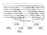
- FIG. 20 shows an example of the operation of the image pickup apparatus having the first frame memory 171 and the second frame memory 172.
- FIG. 20 schematically shows the operation in each of the kth, (k + 1) th, and (k + 2) th frame periods.
- k-th frame period from the time t6 which is the start of the reading of the row 0 pixel related reset signal R 0, is the completion of the reading of the pixel signals relating to pixels of the fifth row R 5 It is a period up to time t14, and its length is eight times as long as the 1H period. Of these, the pixel signal reading period starts at time t8 and ends at time t14 based on the rise of the VD pulse.
- a part of the reset signal reading period and a part of the pixel signal reading period overlap.
- the first digital signal obtained by analog-digital conversion of the read reset signal is temporarily held in the first frame memory 171 and obtained by analog-digital conversion of the read pixel signal.
- the second digital signal is temporarily held in the second frame memory 172.
- the storage of the first digital signal and the second digital signal in the frame memory can be executed in line units. Therefore, while allowing a part of the reset signal reading period and a part of the pixel signal reading period to overlap, for example, the reset signal reading and the pixel signal reading for all the rows of the plurality of pixel Px can be performed. After completion, the difference between the first digital signal and the second digital signal can be executed. Therefore, it is advantageous for shortening the exposure period. According to this embodiment, for example, the exposure period can be shorter than the 1V period.
- the length of the (k + 1) th frame period is 10 times that of the 1H period, whereas the kth frame period has eight times the length of the 1H period, and the (k + 2) th frame period.
- the length of the frame period is 12 times that of the 1H period.
- the readout of the reset signal of each line can be shifted backward to twice the 1H period to shorten the exposure period for the (k + 1) th and (k + 2) th frame periods.
- the shortening of the exposure period is useful for shooting when the environment suddenly shifts from a dark environment to a bright environment.
- the exposure period when the exposure period is extended, the period for reading the reset signal for the previous frame period and the period for reading the reset signal for the later frame period overlap between two consecutive frame periods. It can happen. In this case, regarding the reading of the reset signal in one of the two frame periods, it may not be possible to properly read the reset signal for some lines. Therefore, regarding the extension of the exposure period, the range in which the exposure period can be extended may be set in advance so that the reset signal reading period does not overlap between the two consecutive frame periods. ..
- the reset signal for a pixel in a certain row and the pixel signal for another row in the previous frame period are read, and later. Overlapping with the reading of the reset signal for pixels in yet another row during the frame period of. In such a case, it may not be possible to obtain a reset signal for some rows of a plurality of pixels in either the earlier frame period or the later frame period.
- the acquisition of the reset signal for the previous frame period may be prioritized.
- the pixel signal read from the line where the signal reading period overlaps may be treated as invalid data.
- the reset level acquired for the earlier frame period may be used again for the later frame period.
- the acquisition of the reset signal for the later frame period is prioritized, the pixel signal read from the line where the signal reading period overlaps with respect to the earlier frame period is treated as invalid data or the first.
- the reset level acquired for the frame period immediately before the frame period of is used.
- FIG. 22 schematically shows an example of a signal reading operation in a configuration in which three or more AD conversion circuits are arranged for each row of a plurality of pixels Px.
- the operation shown in FIG. 22 applies, for example, a connection between a pixel and an AD conversion circuit as shown in FIG. 12 to an image pickup apparatus having two frame memories as in the example described with reference to FIG. It is possible under the above configuration.
- a part of the k-th frame period and a part of the (k + 1) -th frame period overlap. Focusing on 1H period for example from time t9 to time t10 in the example shown in FIG. 21, pixels from the k-th reading the first row R 1 of the pixels of the reset signal from the third row R 3 pixels for a frame period The reading of the reset signal from the pixel of the 0th row R0 with respect to the (k + 1) th frame period overlaps with the reading of the signal.
- the pixel of row 0 R 0, the pixel of the first row R 1, the second row R 2 of the pixel, and the third row pixel first output signal each of R 3 1st AD conversion circuit 141, 2nd AD conversion circuit 142, 3rd AD conversion circuit 143 and 4th AD via line S j , 2nd output signal line T j , 3rd output signal line U j and 4th output signal line V j . It is assumed that it is connected to the conversion circuit 144.
- the related (k + 1) th frame period in addition to the pixel signal from the reset signal and the first row of pixels R 1 from the third row R 3 pixels for the k-th frame period, the related (k + 1) th frame period
- the reset signal from the pixel of line 0 R 0 can be read out in parallel via different output signal lines. That is, analog signals can be read out in parallel from three or more rows of a plurality of pixels.
- the analog signals individually read via the first output signal line S j , the second output signal line T j, and the fourth output signal line V j are the first AD conversion circuit 141, the second AD conversion circuit 142, and the fourth AD. It is converted into a digital signal by the conversion circuit 144.
- the digital signals generated by the analog-to-digital conversion for example, the first digital signal corresponding to the reset signal is stored in the first frame memory 171 and the second digital signal corresponding to the pixel signal is the second frame memory. It is stored in 172.
- a data selector 35 is connected to the front stage of the first frame memory 171 and the second frame memory 172 as described with reference to FIGS. 18 and 19. It is possible by doing so.
- FIG. 22 schematically shows still another modification of the imaging device.
- the image pickup apparatus 100H shown in FIG. 22 has an image processing circuit 170B like the imaging apparatus 100D described with reference to FIG. 16, and further has a frequency multiplier 175 connected to the image processing circuit 170B. ..
- the imaging device 100H has no, does not have a second output signal line T j, therefore, the 2AD conversion circuit 142, also including a second interface 162.
- the image processing circuit 170A may be applied instead of the image processing circuit 170B.
- the image pickup apparatus 100H has a plurality of first output signal lines Sj provided corresponding to a plurality of rows of the plurality of pixels Px.
- a readout circuit 20 for two or more pixels belonging to the same row in the imaging region is connected to each of the plurality of first output signal lines Sj .
- the point that a plurality of first output signal lines Sj are connected to the first AD conversion circuit 141 is the same as the examples described so far.
- the frequency multiplier 175 receives the horizontal synchronization signal from the image processing circuit 170B as an input, and generates a pulse train having a period shorter than that of the horizontal synchronization signal. This pulse train has an interval obtained by equally dividing the interval between the pulses of the horizontal synchronization signal, and is sent from the frequency multiplier 175 to the control circuit 220.
- the frequency multiplier 175 is typically a circuit that executes frequency multiplication using a PLL (phase locked loop).
- the frequency multiplier 175 may be a part of the image processing circuit 170B or 170A, or may be a part of the row scanning circuit 130.
- FIG. 23 schematically shows an example of the operation of the image pickup apparatus 100H shown in FIG. 22.
- the third chart from the top schematically shows the pulse of the signal MD output from the frequency multiplier 175.
- the pulse of the signal MD has a period (1/2) times that of the pulse of the horizontal synchronization signal HD.
- a part of the reset signal read-out period and a part of the pixel signal read-out period overlap.
- the pixel signal is read from the pixel of the 0th row R0 in the first half of this 1H period, and the second half of this 1H period is the second.
- Reading of the reset signal from the pixels of line 2 R 2 is being executed. That is, the reading of the pixel signal from the pixel of a certain row belonging to the same column of the plurality of pixels Px and the reading of the reset signal from the pixel of another row are executed within the same 1H period.
- the read reset signal and pixel signal are converted into a first digital signal and a second digital signal by the first AD conversion circuit 141, respectively. Of these, at least the first digital signal is held in the first frame memory 171. At this time, the second digital signal may be held in the second frame memory 172.
- the image processing circuit 170B outputs the difference between the second digital signal and the first digital signal held in the first frame memory 171 for each pixel after the reading of the pixel signals for all the rows is completed. By this difference processing, the influence of the reset noise superimposed on these signals can be substantially canceled.
- a second pulse train having a frequency higher than that of the horizontal sync signal HD pulse may be generated, and the analog signal may be read from the pixels based on the second pulse train.
- the reset noise can be reduced without providing two or more output signal lines in each row of the plurality of pixels Px, as in each of the above examples. The effect of being able to flexibly change the frame rate while canceling the effect can be obtained.
- the reading of the reset signal for a certain frame period precedes the reading of the pixel signal in the frame period immediately before the frame period. Can be done. Therefore, the blanking period between the two frame periods can be shortened and the frame rate can be shortened while the circuit configuration is simpler.
- the image pickup apparatus 100H shown in FIG. 22 has an image processing circuit 170B including a first frame memory 171 and a second frame memory 172.
- the above-mentioned data selector 35 may be interposed between the first interface 161 and the image processing circuit 170B.
- an interface that selectively outputs the first digital signal and an interface that selectively outputs the second digital signal are provided, and a data selector 35 is interposed between these interfaces and the first AD conversion circuit 141. You may.
- the reset signal and the pixel signal for a certain pixel in the imaging region can be sequentially converted into a digital signal. Further, by storing the first digital signal corresponding to the reset signal in the frame memory and calculating the difference from the second digital signal corresponding to the pixel signal, the frame rate is shortened and the influence of the reset noise is affected. It is possible to achieve both substantial cancellation.
- the row scanning circuit 130, the control circuit 220, the first AD conversion circuit 141, the second AD conversion circuit 142, the first digital memory 151, the second digital memory 152, the first interface 161 and the second interface 162 illustrates a configuration arranged on a semiconductor substrate 110 on which a plurality of pixels Px are formed. That is, the semiconductor substrate 110 on which a plurality of pixels Px are formed, the row scanning circuit 130, the control circuit 220, the first AD conversion circuit 141, the second AD conversion circuit 142, the first digital memory 151, the second digital memory 152, and the first interface.
- the 161 and the second interface 162 may be provided in the form of a package in which they are integrated.
- a part or all of these circuits may be integrally formed on the semiconductor substrate 110 in addition to the reading circuit 20 of each pixel Px. That is, these circuits can be formed on the semiconductor substrate 110 by applying the same process as the process of forming the reading circuit 20 for each pixel Px.
- the control circuit 220 may be an integrated circuit formed on the semiconductor substrate 110. However, it is not essential that all of these circuits are integrally formed on the semiconductor substrate 110 together with each pixel Px. A part or all of these circuits may be arranged on a substrate different from the semiconductor substrate 110 on which each pixel Px is formed.
- control circuit 220 receives the setting related to the exposure time from the image processing circuits 170A and 170B according to the processing result of the image processing circuits 170A and 170B, and receives the drive signal according to the setting related to the exposure time from the row scanning circuit 130 and the first AD conversion. It may be configured to supply to the circuit 141, the second AD conversion circuit 142, and the like.
- the image processing circuits 170A and 170B may be provided in the image pickup apparatus in the form of a chip or a package separate from the circuit group arranged on the semiconductor substrate 110. These substrates, including the semiconductor substrate 110, may be provided in a laminated form.
- the first frame memory 171 and / or the second frame memory 172 may be arranged in the image pickup apparatus in the form of a chip or package separate from the image processing circuit 170A or 170B.
- the image processing circuits 170A and 170B may be arranged on the semiconductor substrate 110.
- the image processing circuits 170A and 170B may be a part of the control circuit 220.
- the image processing circuits 170A, 170B or the control circuit 220 may be configured to perform processing such as distance measurement calculation and wavelength information separation.
- the image pickup apparatus may be provided in the form of a package in which a semiconductor substrate 110 on which a plurality of pixels Px are formed and an image processing circuit 170A or 170B are integrated.
- the image pickup apparatus according to the embodiment of the present disclosure may be in the form of an image sensor chip or in the form of a camera.
- Embodiments of the present disclosure include, for example, digital still cameras, digital video cameras, medical cameras, security cameras, cameras mounted on vehicles, ranging cameras, microscope cameras, unmanned aircraft cameras called drones, and robots. It can be used for various cameras such as cameras and camera systems.
- the vehicle-mounted camera can be used, for example, as an input to a control device for the vehicle to travel safely. Alternatively, it can be used to assist the operator in driving the vehicle safely.
- Photoelectric conversion unit 20 Read circuit 31, 33 First signal switching circuit 34 Second signal switching circuit 35 Data selector 100A to 100H Imaging device 110
- Semiconductor board 120 Circuit board 130 line scanning circuit 141 First AD conversion circuit 142 Second AD conversion circuit 143 3rd AD conversion circuit 144 4th AD conversion circuit 145
- Column signal processing circuit 161 1st interface 162 2nd interface 170A, 170B
- Image processing circuit 171 1st frame memory 172 2nd frame memory 175
- Frequency multiplier 220 Control circuit Px, Px1 to Px4 Pixel S j 1st output signal line T j 2nd output signal line U j 3rd output signal line V j 4th output signal line
Landscapes
- Engineering & Computer Science (AREA)
- Multimedia (AREA)
- Signal Processing (AREA)
- Transforming Light Signals Into Electric Signals (AREA)
- Solid State Image Pick-Up Elements (AREA)
Priority Applications (5)
| Application Number | Priority Date | Filing Date | Title |
|---|---|---|---|
| JP2021536838A JP7603261B2 (ja) | 2019-08-01 | 2020-06-24 | 撮像装置および撮像装置の駆動方法 |
| CN202080032704.0A CN113906733B (zh) | 2019-08-01 | 2020-06-24 | 摄像装置和摄像装置的驱动方法 |
| US17/543,830 US11825223B2 (en) | 2019-08-01 | 2021-12-07 | Imaging device and driving method thereof |
| US18/486,802 US12302015B2 (en) | 2019-08-01 | 2023-10-13 | Imaging device and driving method thereof |
| JP2024208872A JP2025041645A (ja) | 2019-08-01 | 2024-11-29 | 撮像装置の駆動方法 |
Applications Claiming Priority (2)
| Application Number | Priority Date | Filing Date | Title |
|---|---|---|---|
| JP2019142101 | 2019-08-01 | ||
| JP2019-142101 | 2019-08-01 |
Related Child Applications (1)
| Application Number | Title | Priority Date | Filing Date |
|---|---|---|---|
| US17/543,830 Continuation US11825223B2 (en) | 2019-08-01 | 2021-12-07 | Imaging device and driving method thereof |
Publications (1)
| Publication Number | Publication Date |
|---|---|
| WO2021019972A1 true WO2021019972A1 (ja) | 2021-02-04 |
Family
ID=74228469
Family Applications (1)
| Application Number | Title | Priority Date | Filing Date |
|---|---|---|---|
| PCT/JP2020/024748 Ceased WO2021019972A1 (ja) | 2019-08-01 | 2020-06-24 | 撮像装置および撮像装置の駆動方法 |
Country Status (4)
| Country | Link |
|---|---|
| US (2) | US11825223B2 (https=) |
| JP (2) | JP7603261B2 (https=) |
| CN (1) | CN113906733B (https=) |
| WO (1) | WO2021019972A1 (https=) |
Cited By (6)
| Publication number | Priority date | Publication date | Assignee | Title |
|---|---|---|---|---|
| JP2023072534A (ja) * | 2021-11-12 | 2023-05-24 | キヤノン株式会社 | 光電変換装置及び機器 |
| JP2023090117A (ja) * | 2021-12-17 | 2023-06-29 | キヤノン株式会社 | 光電変換装置及び撮像システム |
| WO2024219220A1 (ja) * | 2023-04-17 | 2024-10-24 | パナソニックIpマネジメント株式会社 | 撮像装置および撮像装置の駆動方法 |
| WO2025163993A1 (ja) * | 2024-01-29 | 2025-08-07 | パナソニックIpマネジメント株式会社 | 撮像装置およびカメラシステム |
| WO2025192217A1 (ja) * | 2024-03-15 | 2025-09-18 | パナソニックIpマネジメント株式会社 | 撮像装置およびカメラシステム |
| WO2025197260A1 (ja) * | 2024-03-18 | 2025-09-25 | パナソニックIpマネジメント株式会社 | 撮像装置およびカメラシステム |
Families Citing this family (2)
| Publication number | Priority date | Publication date | Assignee | Title |
|---|---|---|---|---|
| JP7603261B2 (ja) * | 2019-08-01 | 2024-12-20 | パナソニックIpマネジメント株式会社 | 撮像装置および撮像装置の駆動方法 |
| JP7755407B2 (ja) * | 2021-08-04 | 2025-10-16 | キヤノン株式会社 | 光電変換装置 |
Citations (4)
| Publication number | Priority date | Publication date | Assignee | Title |
|---|---|---|---|---|
| JP2010232804A (ja) * | 2009-03-26 | 2010-10-14 | Victor Co Of Japan Ltd | 固体撮像素子及びそれを用いた固体撮像装置 |
| JP2017055382A (ja) * | 2015-09-10 | 2017-03-16 | キヤノン株式会社 | 撮像装置及び撮像システム |
| JP2017126846A (ja) * | 2016-01-13 | 2017-07-20 | ソニー株式会社 | 撮像素子、撮像素子の駆動方法、並びに、電子機器 |
| WO2017169480A1 (ja) * | 2016-03-31 | 2017-10-05 | 株式会社ニコン | 撮像素子および撮像装置 |
Family Cites Families (26)
| Publication number | Priority date | Publication date | Assignee | Title |
|---|---|---|---|---|
| JP3792441B2 (ja) | 1999-06-28 | 2006-07-05 | 日本電気株式会社 | 信号処理装置 |
| JP2001358992A (ja) | 2000-06-16 | 2001-12-26 | Yokogawa Electric Corp | 相関二重サンプリング回路 |
| US7456879B2 (en) * | 2003-08-29 | 2008-11-25 | Aptina Imaging Corporation | Digital correlated double sampling using dual analog path |
| GB2424781B (en) * | 2005-03-30 | 2007-11-28 | Micron Technology Inc | High density row ram for column parallel CMOS image sensors |
| JP4873385B2 (ja) | 2006-07-19 | 2012-02-08 | オリンパス株式会社 | 固体撮像装置 |
| US8089522B2 (en) * | 2007-09-07 | 2012-01-03 | Regents Of The University Of Minnesota | Spatial-temporal multi-resolution image sensor with adaptive frame rates for tracking movement in a region of interest |
| JP2009141673A (ja) | 2007-12-06 | 2009-06-25 | Sensor Technology Co Ltd | 相関二重サンプリング回路 |
| US8174603B2 (en) * | 2008-05-01 | 2012-05-08 | Alexander Krymski | Image sensors and methods with antiblooming channels and two side driving of control signals |
| JP2011211535A (ja) * | 2010-03-30 | 2011-10-20 | Sony Corp | 固体撮像素子およびカメラシステム |
| JP2011228648A (ja) | 2010-03-31 | 2011-11-10 | Fujifilm Corp | 撮像素子 |
| JP2012044536A (ja) * | 2010-08-20 | 2012-03-01 | Olympus Corp | 読出し制御装置、読出し制御方法、プログラム、撮像装置および固体撮像装置 |
| JP5806539B2 (ja) * | 2011-07-22 | 2015-11-10 | ルネサスエレクトロニクス株式会社 | 固体撮像装置 |
| US8599284B2 (en) * | 2011-10-11 | 2013-12-03 | Omnivision Technologies, Inc. | High dynamic range sub-sampling architecture |
| US20140375852A1 (en) * | 2013-06-20 | 2014-12-25 | Canon Kabushiki Kaisha | Solid-state imaging apparatus, method of manufacturing the same, camera, imaging device, and imaging apparatus |
| JP2015106908A (ja) * | 2013-12-03 | 2015-06-08 | 株式会社リコー | カラム読出し回路および固体撮像装置 |
| JP2015204583A (ja) * | 2014-04-16 | 2015-11-16 | キヤノン株式会社 | 撮像装置 |
| JP2016012903A (ja) | 2014-06-02 | 2016-01-21 | ソニー株式会社 | 撮像素子、撮像方法、および電子機器 |
| JP2016144151A (ja) * | 2015-02-04 | 2016-08-08 | キヤノン株式会社 | 固体撮像装置の駆動方法、固体撮像装置およびカメラ |
| US10079988B2 (en) * | 2015-07-07 | 2018-09-18 | Panasonic Intellectual Property Management Co., Ltd. | Imaging device including pixel |
| JP2017135693A (ja) * | 2016-01-21 | 2017-08-03 | パナソニックIpマネジメント株式会社 | 撮像装置 |
| JP6816416B2 (ja) * | 2016-09-06 | 2021-01-20 | リコーイメージング株式会社 | 撮像装置 |
| JP6904772B2 (ja) * | 2017-04-26 | 2021-07-21 | キヤノン株式会社 | 固体撮像装置及びその駆動方法 |
| JP6976776B2 (ja) * | 2017-08-31 | 2021-12-08 | キヤノン株式会社 | 固体撮像装置、撮像システム、及び移動体 |
| JP7023685B2 (ja) * | 2017-11-30 | 2022-02-22 | キヤノン株式会社 | 撮像装置、撮像システム、移動体 |
| JP7358079B2 (ja) | 2019-06-10 | 2023-10-10 | キヤノン株式会社 | 撮像装置、撮像システムおよび半導体チップ |
| JP7603261B2 (ja) * | 2019-08-01 | 2024-12-20 | パナソニックIpマネジメント株式会社 | 撮像装置および撮像装置の駆動方法 |
-
2020
- 2020-06-24 JP JP2021536838A patent/JP7603261B2/ja active Active
- 2020-06-24 CN CN202080032704.0A patent/CN113906733B/zh active Active
- 2020-06-24 WO PCT/JP2020/024748 patent/WO2021019972A1/ja not_active Ceased
-
2021
- 2021-12-07 US US17/543,830 patent/US11825223B2/en active Active
-
2023
- 2023-10-13 US US18/486,802 patent/US12302015B2/en active Active
-
2024
- 2024-11-29 JP JP2024208872A patent/JP2025041645A/ja active Pending
Patent Citations (4)
| Publication number | Priority date | Publication date | Assignee | Title |
|---|---|---|---|---|
| JP2010232804A (ja) * | 2009-03-26 | 2010-10-14 | Victor Co Of Japan Ltd | 固体撮像素子及びそれを用いた固体撮像装置 |
| JP2017055382A (ja) * | 2015-09-10 | 2017-03-16 | キヤノン株式会社 | 撮像装置及び撮像システム |
| JP2017126846A (ja) * | 2016-01-13 | 2017-07-20 | ソニー株式会社 | 撮像素子、撮像素子の駆動方法、並びに、電子機器 |
| WO2017169480A1 (ja) * | 2016-03-31 | 2017-10-05 | 株式会社ニコン | 撮像素子および撮像装置 |
Cited By (9)
| Publication number | Priority date | Publication date | Assignee | Title |
|---|---|---|---|---|
| JP2023072534A (ja) * | 2021-11-12 | 2023-05-24 | キヤノン株式会社 | 光電変換装置及び機器 |
| JP7580362B2 (ja) | 2021-11-12 | 2024-11-11 | キヤノン株式会社 | 光電変換装置及び機器 |
| US12407947B2 (en) | 2021-11-12 | 2025-09-02 | Canon Kabushiki Kaisha | Photoelectric conversion apparatus and equipment |
| JP2023090117A (ja) * | 2021-12-17 | 2023-06-29 | キヤノン株式会社 | 光電変換装置及び撮像システム |
| JP7838953B2 (ja) | 2021-12-17 | 2026-04-01 | キヤノン株式会社 | 光電変換装置及び撮像システム |
| WO2024219220A1 (ja) * | 2023-04-17 | 2024-10-24 | パナソニックIpマネジメント株式会社 | 撮像装置および撮像装置の駆動方法 |
| WO2025163993A1 (ja) * | 2024-01-29 | 2025-08-07 | パナソニックIpマネジメント株式会社 | 撮像装置およびカメラシステム |
| WO2025192217A1 (ja) * | 2024-03-15 | 2025-09-18 | パナソニックIpマネジメント株式会社 | 撮像装置およびカメラシステム |
| WO2025197260A1 (ja) * | 2024-03-18 | 2025-09-25 | パナソニックIpマネジメント株式会社 | 撮像装置およびカメラシステム |
Also Published As
| Publication number | Publication date |
|---|---|
| US20220094869A1 (en) | 2022-03-24 |
| US12302015B2 (en) | 2025-05-13 |
| CN113906733B (zh) | 2024-06-21 |
| CN113906733A (zh) | 2022-01-07 |
| US20240040277A1 (en) | 2024-02-01 |
| JPWO2021019972A1 (https=) | 2021-02-04 |
| JP7603261B2 (ja) | 2024-12-20 |
| JP2025041645A (ja) | 2025-03-26 |
| US11825223B2 (en) | 2023-11-21 |
Similar Documents
| Publication | Publication Date | Title |
|---|---|---|
| JP7603261B2 (ja) | 撮像装置および撮像装置の駆動方法 | |
| US9843751B2 (en) | Solid-state image sensor and camera system | |
| TWI504256B (zh) | 固態成像裝置,其訊號處理方法,及電子設備 | |
| JP6239975B2 (ja) | 固体撮像装置及びそれを用いた撮像システム | |
| KR102389417B1 (ko) | 고체 촬상 소자 및 촬상 장치 | |
| JP7486080B2 (ja) | 撮像装置 | |
| KR102325497B1 (ko) | 촬상 소자 및 촬상 장치 | |
| KR101598748B1 (ko) | 고체 촬상 장치 | |
| TW201541963A (zh) | 固體攝像裝置 | |
| JPH11103420A (ja) | 固体撮像素子およびその駆動方法 | |
| JP6150508B2 (ja) | 撮像装置及び撮像システム | |
| US10944924B2 (en) | Image sensor and electronic camera | |
| US10602088B2 (en) | Solid-state imaging device and imaging apparatus | |
| CN105704401B (zh) | 摄像装置的驱动方法以及摄像装置 | |
| JP2014016382A (ja) | 固体撮像装置、電子機器、および画素読み出し方法 | |
| WO2024219220A1 (ja) | 撮像装置および撮像装置の駆動方法 | |
| US10944926B2 (en) | Solid-state imaging element, method for driving solid-state imaging element, and electronic apparatus | |
| US20140048690A1 (en) | Solid-state imaging device | |
| JP2026013319A (ja) | 光電変換装置、撮像装置、機器 | |
| WO2025192217A1 (ja) | 撮像装置およびカメラシステム | |
| JP5980615B2 (ja) | 固体撮像装置および撮像装置 | |
| JP2018019193A (ja) | 撮像装置及びその制御方法 | |
| JP2007135227A (ja) | 固体撮像素子および固体撮像素子の駆動方法 |
Legal Events
| Date | Code | Title | Description |
|---|---|---|---|
| 121 | Ep: the epo has been informed by wipo that ep was designated in this application |
Ref document number: 20847344 Country of ref document: EP Kind code of ref document: A1 |
|
| ENP | Entry into the national phase |
Ref document number: 2021536838 Country of ref document: JP Kind code of ref document: A |
|
| NENP | Non-entry into the national phase |
Ref country code: DE |
|
| 122 | Ep: pct application non-entry in european phase |
Ref document number: 20847344 Country of ref document: EP Kind code of ref document: A1 |