WO2021005654A1 - A/d変換回路 - Google Patents
A/d変換回路 Download PDFInfo
- Publication number
- WO2021005654A1 WO2021005654A1 PCT/JP2019/026856 JP2019026856W WO2021005654A1 WO 2021005654 A1 WO2021005654 A1 WO 2021005654A1 JP 2019026856 W JP2019026856 W JP 2019026856W WO 2021005654 A1 WO2021005654 A1 WO 2021005654A1
- Authority
- WO
- WIPO (PCT)
- Prior art keywords
- current
- potential
- amount control
- current amount
- bit
- Prior art date
- Legal status (The legal status is an assumption and is not a legal conclusion. Google has not performed a legal analysis and makes no representation as to the accuracy of the status listed.)
- Ceased
Links
Images










Classifications
-
- H—ELECTRICITY
- H03—ELECTRONIC CIRCUITRY
- H03M—CODING; DECODING; CODE CONVERSION IN GENERAL
- H03M1/00—Analogue/digital conversion; Digital/analogue conversion
- H03M1/12—Analogue/digital converters
- H03M1/34—Analogue value compared with reference values
- H03M1/38—Analogue value compared with reference values sequentially only, e.g. successive approximation type
- H03M1/46—Analogue value compared with reference values sequentially only, e.g. successive approximation type with digital/analogue converter for supplying reference values to converter
- H03M1/466—Analogue value compared with reference values sequentially only, e.g. successive approximation type with digital/analogue converter for supplying reference values to converter using switched capacitors
-
- H—ELECTRICITY
- H03—ELECTRONIC CIRCUITRY
- H03M—CODING; DECODING; CODE CONVERSION IN GENERAL
- H03M1/00—Analogue/digital conversion; Digital/analogue conversion
- H03M1/06—Continuously compensating for, or preventing, undesired influence of physical parameters
- H03M1/08—Continuously compensating for, or preventing, undesired influence of physical parameters of noise
-
- H—ELECTRICITY
- H03—ELECTRONIC CIRCUITRY
- H03M—CODING; DECODING; CODE CONVERSION IN GENERAL
- H03M1/00—Analogue/digital conversion; Digital/analogue conversion
- H03M1/12—Analogue/digital converters
- H03M1/34—Analogue value compared with reference values
- H03M1/38—Analogue value compared with reference values sequentially only, e.g. successive approximation type
- H03M1/46—Analogue value compared with reference values sequentially only, e.g. successive approximation type with digital/analogue converter for supplying reference values to converter
- H03M1/466—Analogue value compared with reference values sequentially only, e.g. successive approximation type with digital/analogue converter for supplying reference values to converter using switched capacitors
- H03M1/468—Analogue value compared with reference values sequentially only, e.g. successive approximation type with digital/analogue converter for supplying reference values to converter using switched capacitors in which the input S/H circuit is merged with the feedback DAC array
Definitions
- the present invention relates to a sequential comparison type A / D conversion circuit.
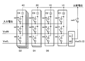
- the CDAC includes a capacitor C1-C4 whose capacitance value is weighted to 2 nC such as 1C, 2C, and 4C, a switch swA1-swA4, swH1-swH4, swL1-swL4, and a reference power supply (reference power supply).
- VrefH / VrefL a series circuit including a resistor R1 and a resistor R2 that generate a 1/2 potential of a reference power source.
- the switches swA1-swA4, swH1-swH4, and swL1-swL4 are analog switches including MOS-FETs M1 and M2 and an inverter IN1.
- the CDAC has, for example, 3-bit bit circuits D2, D1, D0.
- the switches swA1-swA4 shown in FIG. 15 are turned on.
- the operation of inputting the input potential is called "sampling operation".
- the input potential and the comparative potential are connected via the capacitors C4-C1 shown by 4C, 2C, 1C and 1C. Charges due to the difference between the input potential and the comparative potential are accumulated in the capacitors C4-C1.
- the switches swH1-swH3 installed in each of the bit circuits D2, D1 and D0 are turned off, and the switch swH4 is turned on. Also, the switch swL1-swL3 is turned on and the switch swL4 is turned off. Observe the comparative potential when the reference power supply VrefH or VrefL is applied to the capacitors C1-C4.
- the comparator turns on, for example, the switch swH of the bit circuit D2 and the switch swL of the bit circuits D1 and D0, the comparison potential is compared with the reference potential which is 1/2 potential of the reference power supply Vref.
- the comparator has a digital value of 100 (binary) corresponding to the input potential. That is, the bit circuit D2 outputs "1", the bit circuit D1 outputs "0", and the bit circuit D0 outputs "0". This is the conversion result of the A / D conversion circuit.
- the potentials of the reference power supplies VrefH and VrefL need to be the intended correct potentials.
- An object of the present invention is to provide an A / D conversion circuit capable of suppressing the noise voltage and reducing the error.
- the A / D conversion circuit of the present invention includes a digital / analog converter that generates a comparative potential based on the potential obtained by sampling and holding the input potential, the digital value, and the reference power supply, and the comparison is performed. It is an A / D conversion circuit that compares a potential with a reference potential generated based on the reference power source, converts the comparative potential into the digital value, and outputs the converted digital value to the digital / analog converter.
- the digital / analog converter is a capacitor in which the comparative current is output at one end and the capacitance value increases from the lower bits of a plurality of bits to the upper bits, and the first switch in which the input current is applied to the other end of the capacitor.
- a plurality of bit circuits in which a series circuit of a second switch and a current amount control element is provided between the other end of the capacitor and the reference power supply corresponding to the plurality of bits, and each of the plurality of bit circuits.
- a current amount control unit for controlling the amount of current flowing through the current amount control element provided in the bit circuit is provided, and the current amount control unit has the second switch in order from the upper bit in each bit circuit according to the digital value.
- the noise current proportional to the charge flowing from the capacitor to the reference power supply becomes equal to or more than an allowable value.
- the noise current is limited to less than an allowable value.
- the noise current is limited to less than the permissible value by applying a current control potential to the current amount control element in any of the bit circuits.
- the noise current to the reference power supply can be made less than the allowable value. That is, it is possible to provide an A / D conversion circuit capable of suppressing the noise voltage to a small value and reducing the error.
- FIG. 1 is an overall configuration diagram of the A / D conversion circuit of the first embodiment.
- FIG. 2 is a diagram showing a configuration of a CDAC in the A / D conversion circuit of the first embodiment.
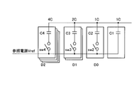
- FIG. 3 is a diagram showing a bit circuit in which a series circuit of a capacitor and a switch provided between the reference power supply and the comparative potential of the CDAC of the first embodiment is provided for each bit.
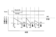
- FIG. 4 is a diagram showing a temporal change in noise current proportional to the electric charge flowing from the capacitor to the reference power supply when the switch is turned on in order from the high-order bit in each bit circuit shown in FIG. FIG.
- FIG. 5 is a diagram showing a plurality of bit circuits in which a series circuit of a switch and a current amount control element is provided between the capacitor and the reference power supply.
- FIG. 6 is a diagram showing a temporal change in noise current when the current flowing through the current amount control element is limited when the switch is turned on in order from the upper bit in the plurality of bit circuits shown in FIG.
- FIG. 7 is a diagram for explaining a problem that occurs when a constant current is applied when each switch of each bit circuit is turned on.
- FIG. 8 is a diagram showing a constant current control potential applied to the current amount control element for a certain period of time when the switch is turned on.
- FIG. 9 is a diagram showing how the establishment time becomes longer when a constant current control potential is applied to the current amount control element.
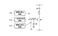
- FIG. 10 is a block diagram of a main part of the A / D conversion circuit of the second embodiment.
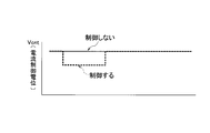
- FIG. 11 is a diagram showing the current control potential when the value is increased or decreased with respect to a constant value.
- FIG. 12 is a diagram showing how the establishment time is shortened when the variable current control potential shown in FIG. 11 is applied to the current amount control element.
- FIG. 13 is a diagram showing a configuration of a conventional CDAC.
- FIG. 14 is a diagram showing the configuration of each switch in the conventional CDAC.
- FIG. 15 is a diagram showing a sampling operation of the input potential when the switch of the conventional CDAC is turned on.
- FIG. 16 is a diagram showing a hold operation of the electric charge stored in the capacitor of the conventional CDAC.
- FIG. 17 is a diagram showing the results of analog / digital conversion of the conventional CDAC.
- FIG. 1 is an overall configuration diagram of the A / D conversion circuit of the first embodiment.
- the A / D conversion circuit includes an ADC overall control unit 1, a CDAC 10, a comparator 20, and a sequential comparison data generator 30.
- the ADC overall control unit 1 controls the entire ADC, and outputs the sampling control signal SCS to the switches swA1-swA4 of the CDAC10.
- the CDAC 10 samples the input potential and generates a comparative potential based on the potential held in the capacitor, the digital value, and the potential of the reference power supply Vref.
- the comparator 20 compares the comparative potential from the CDAC 10 with the reference potential Vref / 2 generated based on the reference power supply Vref, and converts the comparative potential into a digital value.
- the sequential comparison data generator 30 stores the digital value converted by the comparator 20 in a register (not shown) and outputs the digital value stored in the register to the CDAC 10 as switch signals swH and swL.
- FIG. 2 is a diagram showing a configuration of CDAC in the A / D conversion circuit of the first embodiment.
- the A / D conversion circuit is a sequential comparison type A / D conversion circuit that uses a CDAC that includes a capacitance for generating a comparison potential.
- the CDAC further provides a switch swH1-swH4 and a current amount control element QH1-QH4 between the capacitor C1-C4 and the reference power supply VrefH with respect to the CDAC shown in FIG. 13, and provides the capacitor C1-C4 and the reference power supply VrefL. It is characterized in that a switch swL1-swL4 and a current amount control element QL1-QL4 are provided between the two.
- a comparative potential is output to one end of the capacitors C2-C4, and the capacitance value increases as the lower bits of the plurality of bits go to the upper bits.
- an input potential is applied to the other end of the capacitors C1-C4.
- a bit circuit D1 including a capacitor C2, a switch swH2, a current amount control element QH2, a switch swL2, and a bit circuit D0 including a current amount control element QL2 are provided.
- the current amount control unit 11 controls the amount of current flowing through the current amount control elements QH1-QH4 and QL1-QL4.
- the current amount control elements QH1-QH4 and QL1-QL4 are made of, for example, MOSFETs.
- the current amount control elements QH1-QH4 and QL1-QL4 are also referred to as current amount control elements Q1-Q4.
- the switches swH and swL input a digital value 1 or 0 from the sequential comparison data generator 30, turn on by the digital value 1, and turn off by the digital value 0.
- the current amount control unit 11 When the current amount control unit 11 is turned on in the order of switches swH4, swH3, swH2, swH1 (switches swL4, swL3, swL2, swL1) in order from the upper bit in each bit circuit D2, D1, D0, the current amount control unit 11 is a capacitor.
- the noise current is limited to less than the permissible value by applying the current control potential to the current amount control element QH4 (QL4).
- the current amount control unit 11 turns on the current amount control element QH4 (QL4) during the period when the switches swH3, swH2 (swL3, swL2) in the bit circuits D1 and D0 excluding any of the bit circuits D2 are turned on. Do not limit the amount of current by letting it.
- FIG. 3 shows a bit circuit in which a series circuit of the capacitor C4-C2 provided between the reference power supply Vref and the comparative potential and the switch sw4-sw2 is provided bit by bit.
- FIG. 4 shows the temporal change of the noise current proportional to the electric charge flowing from the capacitors C4, C3, and C2 to the reference power supply Vref when the switches sw4, sw3, and sw2 are turned on in order from the bit circuit of the upper bit.
- the sequential comparison type A / D conversion circuit
- the CDAC is operated, the comparison potential is compared with the reference potential, and the process of determining the digital value of the next CDAC is repeated.
- the digital value is obtained from the higher-order (larger value) bit. Therefore, when considering the noise of the reference power supply, the model in which the switches sw4, sw3, and sw2 shown in FIG. 3 are turned on in order may be considered. ..
- the noise current and noise voltage are when the noise current (noise voltage) when the switch sw4 is turned on is 4, and when the switch sw3 is turned on.
- the noise current (noise voltage) of is 2, and the noise current (noise voltage) when the switch sw2 is turned on is 1. Therefore, in order to suppress noise, focus on the operation of the high-order bits.
- FIG. 4 shows the case where the allowable current is exceeded.
- the switch sw4 of the high-order bit is turned on at time t1
- the noise current flows beyond the permissible value and becomes zero at time t2.
- the potential comparison between the comparative potential and the reference potential is performed.
- the switch sw3 is turned on at time t4
- the noise current flows below the permissible value and becomes zero at time t5.
- the potential comparison between the comparative potential and the reference potential is performed.
- the switch sw2 is turned on at time t7, the noise current flows below the permissible value and becomes zero at time t8.
- the potential comparison between the comparative potential and the reference potential is performed.
- the noise current to the reference power supply Vref can be made less than the allowable value. That is, it is possible to provide an A / D conversion circuit capable of suppressing the noise voltage to a small value and reducing the error.
- the process of delaying the potential comparison time of the bit circuit is performed.
- This process has an element that slows down the conversion speed of the A / D conversion circuit.
- the conversion of all bits is not slowed down, but only the establishment time of the bit circuit with the current limit is slowed down. Therefore, in the case where the solution of the noise problem of the reference power supply is prioritized, compared with the conventional technology, This process has great advantages.
- the noise current exceeds the permissible value when the switch sw4 is turned on, and there is no problem when the switches sw3 and sw2 are turned on. It is assumed that the on-resistance of the switch sw4 is designed to suppress the current. Similar to the present invention, this design will be able to suppress the noise current (noise voltage) due to the switch sw4 in exchange for lengthening the establishment time of the bit circuit D2 when the switch sw4 is turned on.
- the current amount control unit 11 limits the noise current to less than the permissible value by applying the current control potential to the current amount control element Q4 during the period when the switch sw4 is turned on.
- the current amount of the current amount control element Q4 is not limited during the period when the switches sw3 and sw2 are turned on.
- the enactment time will be increased only when the current is limited.
- the current amount control elements Q1-Q4 are used during the period from when the CDAC switch is turned on to when the CDAC starts operating and when the operation is completed. A constant current control potential was applied to suppress the current.
- the current amount control elements Q1-Q4 behave like a resistor and suppress the current. As a result, a large current does not flow, but the time at which the current ends, that is, the time for establishing the CDAC becomes long as shown in FIG.
- the problem to be solved in the second embodiment is to suppress the peak of the noise current (noise voltage)
- the relationship between the current and the time is shaped like a rectangle, and the area (charge amount) is the same.
- the height (current peak) is low.
- the A / D conversion circuit of the second embodiment includes a constant voltage generation circuit 11a, a voltage reduction generation circuit 11b, a voltage increase generation circuit 11c, and a switch 13 shown in FIG.
- the constant voltage generation circuit 11a, the voltage reduction generation circuit 11b, and the voltage increase generation circuit 11c are provided in the current amount control unit 11.
- the switch 13 switches and selects the constant voltage generation circuit 11a, the voltage reduction generation circuit 11b, and the voltage increase generation circuit 11c.
- the constant voltage generation circuit 11a applies the constant current control potential Va shown in FIG. 11 to the current amount control element Q4 via the switch 13 before the time t11.
- the voltage reduction generation circuit 11b applies a current control potential Vb, which is smaller than the current control potential Va, to the current amount control element Q4 via the switch 13.
- the voltage boosting circuit 11c applies the current control potential Vc, which is larger than the current control potential Va, to the current amount control element Q4 via the switch 13.
- the establishment time when the current control potential is constant and not variably controlled is substantially the same as the establishment time when the current control potential is variably controlled. Therefore, it is possible to realize an A / D conversion circuit having a small noise current (noise voltage) without impairing the establishment time of the CDAC and therefore the conversion time of the A / D conversion circuit.
- the present invention is applicable to CDAC.
- ADC overall control unit 10 CDAC 11 Current amount control unit 20 Comparator 30 Sequential comparison data generator C1-C4 Capacitor swA0-swA4, swH1-swH4, swL1-swL4 Switch QH1-QH4, QL1-QL4 Current amount control element VrefH, VrefL Reference power supply
Landscapes
- Engineering & Computer Science (AREA)
- Theoretical Computer Science (AREA)
- Analogue/Digital Conversion (AREA)
Priority Applications (4)
| Application Number | Priority Date | Filing Date | Title |
|---|---|---|---|
| PCT/JP2019/026856 WO2021005654A1 (ja) | 2019-07-05 | 2019-07-05 | A/d変換回路 |
| JP2021530353A JP7380688B2 (ja) | 2019-07-05 | 2019-07-05 | A/d変換回路 |
| CN201980097912.6A CN114128151B (zh) | 2019-07-05 | 2019-07-05 | A/d转换电路 |
| US17/563,109 US11689211B2 (en) | 2019-07-05 | 2021-12-28 | Analog-to-digital converter |
Applications Claiming Priority (1)
| Application Number | Priority Date | Filing Date | Title |
|---|---|---|---|
| PCT/JP2019/026856 WO2021005654A1 (ja) | 2019-07-05 | 2019-07-05 | A/d変換回路 |
Related Child Applications (1)
| Application Number | Title | Priority Date | Filing Date |
|---|---|---|---|
| US17/563,109 Continuation US11689211B2 (en) | 2019-07-05 | 2021-12-28 | Analog-to-digital converter |
Publications (1)
| Publication Number | Publication Date |
|---|---|
| WO2021005654A1 true WO2021005654A1 (ja) | 2021-01-14 |
Family
ID=74113948
Family Applications (1)
| Application Number | Title | Priority Date | Filing Date |
|---|---|---|---|
| PCT/JP2019/026856 Ceased WO2021005654A1 (ja) | 2019-07-05 | 2019-07-05 | A/d変換回路 |
Country Status (4)
| Country | Link |
|---|---|
| US (1) | US11689211B2 (https=) |
| JP (1) | JP7380688B2 (https=) |
| CN (1) | CN114128151B (https=) |
| WO (1) | WO2021005654A1 (https=) |
Citations (4)
| Publication number | Priority date | Publication date | Assignee | Title |
|---|---|---|---|---|
| JP2002374169A (ja) * | 2001-06-13 | 2002-12-26 | Matsushita Electric Ind Co Ltd | 逐次比較型a/d変換器 |
| JP2005295315A (ja) * | 2004-04-01 | 2005-10-20 | Oki Electric Ind Co Ltd | 逐次比較型a/d変換器およびコンパレータ |
| US20100271245A1 (en) * | 2009-04-27 | 2010-10-28 | Linear Technology Corporation | Complex-admittance digital-to-analog converter |
| US20190068179A1 (en) * | 2017-08-29 | 2019-02-28 | Realtek Semiconductor Corporation | Data converter and impedance matching control method thereof |
Family Cites Families (18)
| Publication number | Priority date | Publication date | Assignee | Title |
|---|---|---|---|---|
| US4200863A (en) * | 1977-10-03 | 1980-04-29 | The Regents Of The University Of California | Weighted capacitor analog/digital converting apparatus and method |
| US4350975A (en) * | 1980-07-18 | 1982-09-21 | American Microsystems, Inc. | Dual bandwidth autozero loop for a voice frequency CODEC |
| US4803462A (en) * | 1987-08-11 | 1989-02-07 | Texas Instruments Incorporated | Charge redistribution A/D converter with increased common mode rejection |
| JPH04129332A (ja) | 1990-09-20 | 1992-04-30 | Nec Ic Microcomput Syst Ltd | 逐次比較型a/d変換装置 |
| US5675340A (en) * | 1995-04-07 | 1997-10-07 | Iowa State University Research Foundation, Inc. | Charge-redistribution analog-to-digital converter with reduced comparator-hysteresis effects |
| US6130635A (en) * | 1998-08-03 | 2000-10-10 | Motorola Inc. | Method of converting an analog signal in an A/D converter utilizing RDAC precharging |
| US6714151B2 (en) * | 2002-06-21 | 2004-03-30 | Fujitsu Limited | A/D converter |
| US20090021332A1 (en) | 2004-10-08 | 2009-01-22 | Koninklijke Philips Electronics N.V. | Array of capacitors switched by mos transistors |
| JP5050951B2 (ja) * | 2008-03-24 | 2012-10-17 | 富士通セミコンダクター株式会社 | 逐次比較型a/d変換器 |
| WO2009131018A1 (ja) * | 2008-04-25 | 2009-10-29 | キュリアス株式会社 | イメージセンサー用a/d変換器 |
| JP4970365B2 (ja) * | 2008-07-01 | 2012-07-04 | 株式会社東芝 | A/d変換器 |
| JP5287291B2 (ja) * | 2009-01-26 | 2013-09-11 | 富士通セミコンダクター株式会社 | 逐次比較型a/d変換器 |
| FR2943199B1 (fr) * | 2009-03-13 | 2012-12-28 | E2V Semiconductors | Procede de lecture de signal de capteur d'image et capteur d'image. |
| JP2010283484A (ja) * | 2009-06-03 | 2010-12-16 | Mitsumi Electric Co Ltd | 逐次比較型ad変換回路 |
| JP5427663B2 (ja) * | 2010-03-24 | 2014-02-26 | スパンション エルエルシー | A/d変換器 |
| JP5865791B2 (ja) | 2012-07-03 | 2016-02-17 | ルネサスエレクトロニクス株式会社 | A/d変換器、半導体装置 |
| US8766833B1 (en) * | 2013-03-06 | 2014-07-01 | Infineon Technologies Austria Ag | System and method for calibrating a circuit |
| US8860599B1 (en) * | 2013-06-06 | 2014-10-14 | Mediatek Inc. | Analog-to-digital conversion apparatus and method capable of achieving fast settling |
-
2019
- 2019-07-05 CN CN201980097912.6A patent/CN114128151B/zh active Active
- 2019-07-05 WO PCT/JP2019/026856 patent/WO2021005654A1/ja not_active Ceased
- 2019-07-05 JP JP2021530353A patent/JP7380688B2/ja active Active
-
2021
- 2021-12-28 US US17/563,109 patent/US11689211B2/en active Active
Patent Citations (4)
| Publication number | Priority date | Publication date | Assignee | Title |
|---|---|---|---|---|
| JP2002374169A (ja) * | 2001-06-13 | 2002-12-26 | Matsushita Electric Ind Co Ltd | 逐次比較型a/d変換器 |
| JP2005295315A (ja) * | 2004-04-01 | 2005-10-20 | Oki Electric Ind Co Ltd | 逐次比較型a/d変換器およびコンパレータ |
| US20100271245A1 (en) * | 2009-04-27 | 2010-10-28 | Linear Technology Corporation | Complex-admittance digital-to-analog converter |
| US20190068179A1 (en) * | 2017-08-29 | 2019-02-28 | Realtek Semiconductor Corporation | Data converter and impedance matching control method thereof |
Also Published As
| Publication number | Publication date |
|---|---|
| CN114128151A (zh) | 2022-03-01 |
| JP7380688B2 (ja) | 2023-11-15 |
| US20220123761A1 (en) | 2022-04-21 |
| CN114128151B (zh) | 2025-07-25 |
| JPWO2021005654A1 (https=) | 2021-01-14 |
| US11689211B2 (en) | 2023-06-27 |
Similar Documents
| Publication | Publication Date | Title |
|---|---|---|
| US6424283B2 (en) | Segmented high speed and high resolution digital-to-analog converter | |
| CN103548268B (zh) | 用于缩放数模转换器中的切换毛刺的补偿式电流单元 | |
| US8830103B2 (en) | D/A converter | |
| JP2013526179A (ja) | 積分非直線性補正を備えた逐次比較レジスタアナログ・デジタル・コンバータ | |
| JP4299419B2 (ja) | デジタルアナログ変換回路 | |
| US7956785B2 (en) | Return to zero digital to analog converter and converting method thereof | |
| TW202011697A (zh) | 連續逼近暫存器類比數位轉換器的控制電路及控制方法 | |
| JP2008236004A (ja) | D/a変換器 | |
| US20020041246A1 (en) | Device and control structure of multi-level pulse width modulation | |
| KR101270457B1 (ko) | 디지털-아날로그 변환기 | |
| CN117424597A (zh) | 逐次逼近型模数转换器及其实现方法、系统、装置与介质 | |
| JP4648779B2 (ja) | ディジタル・アナログ変換器 | |
| JP2014022763A (ja) | A/d変換器、a/d変換方法 | |
| EP0681372B1 (en) | Digital-to-analog conversion circuit and analog-to-digital conversion device using the circuit | |
| WO2021005654A1 (ja) | A/d変換回路 | |
| JP6643560B2 (ja) | デジタル・アナログコンバータ | |
| WO2022085324A1 (ja) | 逐次比較型アナログ/デジタル変換器 | |
| US9973204B1 (en) | Resistor string digital to analog converter | |
| CN117852471B (zh) | 一种dsp芯片的外围电路、芯片以及控制方法 | |
| TWI865199B (zh) | 用於pam-(2^n-2) 接收器的連續近似式類比至數位轉換器 | |
| KR100282443B1 (ko) | 디지탈/아날로그 컨버터 | |
| KR102873357B1 (ko) | 기준 전압 분배를 이용한 판정 궤환 등화기 및 이를 포함하는 pam-3 수신기 | |
| JPH05145421A (ja) | 基準電圧発生回路 | |
| TWI493878B (zh) | 改善電容合併切換技術的數位類比轉換電路線性度之資料加權平均演算法系統 | |
| JP2024018164A (ja) | 逐次比較型ad変換回路 |
Legal Events
| Date | Code | Title | Description |
|---|---|---|---|
| 121 | Ep: the epo has been informed by wipo that ep was designated in this application |
Ref document number: 19936907 Country of ref document: EP Kind code of ref document: A1 |
|
| ENP | Entry into the national phase |
Ref document number: 2021530353 Country of ref document: JP Kind code of ref document: A |
|
| NENP | Non-entry into the national phase |
Ref country code: DE |
|
| 122 | Ep: pct application non-entry in european phase |
Ref document number: 19936907 Country of ref document: EP Kind code of ref document: A1 |
|
| WWG | Wipo information: grant in national office |
Ref document number: 201980097912.6 Country of ref document: CN |