WO2021005654A1 - A/d conversion circuit - Google Patents
A/d conversion circuit Download PDFInfo
- Publication number
- WO2021005654A1 WO2021005654A1 PCT/JP2019/026856 JP2019026856W WO2021005654A1 WO 2021005654 A1 WO2021005654 A1 WO 2021005654A1 JP 2019026856 W JP2019026856 W JP 2019026856W WO 2021005654 A1 WO2021005654 A1 WO 2021005654A1
- Authority
- WO
- WIPO (PCT)
- Prior art keywords
- current
- potential
- amount control
- current amount
- bit
- Prior art date
Links
Images


Classifications
-
- H—ELECTRICITY
- H03—ELECTRONIC CIRCUITRY
- H03M—CODING; DECODING; CODE CONVERSION IN GENERAL
- H03M1/00—Analogue/digital conversion; Digital/analogue conversion
- H03M1/12—Analogue/digital converters
- H03M1/34—Analogue value compared with reference values
- H03M1/38—Analogue value compared with reference values sequentially only, e.g. successive approximation type
- H03M1/46—Analogue value compared with reference values sequentially only, e.g. successive approximation type with digital/analogue converter for supplying reference values to converter
- H03M1/466—Analogue value compared with reference values sequentially only, e.g. successive approximation type with digital/analogue converter for supplying reference values to converter using switched capacitors
-
- H—ELECTRICITY
- H03—ELECTRONIC CIRCUITRY
- H03M—CODING; DECODING; CODE CONVERSION IN GENERAL
- H03M1/00—Analogue/digital conversion; Digital/analogue conversion
- H03M1/06—Continuously compensating for, or preventing, undesired influence of physical parameters
- H03M1/08—Continuously compensating for, or preventing, undesired influence of physical parameters of noise
-
- H—ELECTRICITY
- H03—ELECTRONIC CIRCUITRY
- H03M—CODING; DECODING; CODE CONVERSION IN GENERAL
- H03M1/00—Analogue/digital conversion; Digital/analogue conversion
- H03M1/12—Analogue/digital converters
- H03M1/34—Analogue value compared with reference values
- H03M1/38—Analogue value compared with reference values sequentially only, e.g. successive approximation type
- H03M1/46—Analogue value compared with reference values sequentially only, e.g. successive approximation type with digital/analogue converter for supplying reference values to converter
- H03M1/466—Analogue value compared with reference values sequentially only, e.g. successive approximation type with digital/analogue converter for supplying reference values to converter using switched capacitors
- H03M1/468—Analogue value compared with reference values sequentially only, e.g. successive approximation type with digital/analogue converter for supplying reference values to converter using switched capacitors in which the input S/H circuit is merged with the feedback DAC array
Definitions
- the present invention relates to a sequential comparison type A / D conversion circuit.
- the CDAC includes a capacitor C1-C4 whose capacitance value is weighted to 2 nC such as 1C, 2C, and 4C, a switch swA1-swA4, swH1-swH4, swL1-swL4, and a reference power supply (reference power supply).
- VrefH / VrefL a series circuit including a resistor R1 and a resistor R2 that generate a 1/2 potential of a reference power source.
- the switches swA1-swA4, swH1-swH4, and swL1-swL4 are analog switches including MOS-FETs M1 and M2 and an inverter IN1.
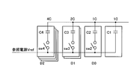
- the CDAC has, for example, 3-bit bit circuits D2, D1, D0.
- the switches swA1-swA4 shown in FIG. 15 are turned on.
- the operation of inputting the input potential is called "sampling operation".
- the input potential and the comparative potential are connected via the capacitors C4-C1 shown by 4C, 2C, 1C and 1C. Charges due to the difference between the input potential and the comparative potential are accumulated in the capacitors C4-C1.
- the switches swH1-swH3 installed in each of the bit circuits D2, D1 and D0 are turned off, and the switch swH4 is turned on. Also, the switch swL1-swL3 is turned on and the switch swL4 is turned off. Observe the comparative potential when the reference power supply VrefH or VrefL is applied to the capacitors C1-C4.
- the comparator turns on, for example, the switch swH of the bit circuit D2 and the switch swL of the bit circuits D1 and D0, the comparison potential is compared with the reference potential which is 1/2 potential of the reference power supply Vref.
- the comparator has a digital value of 100 (binary) corresponding to the input potential. That is, the bit circuit D2 outputs "1", the bit circuit D1 outputs "0", and the bit circuit D0 outputs "0". This is the conversion result of the A / D conversion circuit.
- the potentials of the reference power supplies VrefH and VrefL need to be the intended correct potentials.
- An object of the present invention is to provide an A / D conversion circuit capable of suppressing the noise voltage and reducing the error.
- the A / D conversion circuit of the present invention includes a digital / analog converter that generates a comparative potential based on the potential obtained by sampling and holding the input potential, the digital value, and the reference power supply, and the comparison is performed. It is an A / D conversion circuit that compares a potential with a reference potential generated based on the reference power source, converts the comparative potential into the digital value, and outputs the converted digital value to the digital / analog converter.
- the digital / analog converter is a capacitor in which the comparative current is output at one end and the capacitance value increases from the lower bits of a plurality of bits to the upper bits, and the first switch in which the input current is applied to the other end of the capacitor.
- a plurality of bit circuits in which a series circuit of a second switch and a current amount control element is provided between the other end of the capacitor and the reference power supply corresponding to the plurality of bits, and each of the plurality of bit circuits.
- a current amount control unit for controlling the amount of current flowing through the current amount control element provided in the bit circuit is provided, and the current amount control unit has the second switch in order from the upper bit in each bit circuit according to the digital value.
- the noise current proportional to the charge flowing from the capacitor to the reference power supply becomes equal to or more than an allowable value.
- the noise current is limited to less than an allowable value.
- the noise current is limited to less than the permissible value by applying a current control potential to the current amount control element in any of the bit circuits.
- the noise current to the reference power supply can be made less than the allowable value. That is, it is possible to provide an A / D conversion circuit capable of suppressing the noise voltage to a small value and reducing the error.
- FIG. 1 is an overall configuration diagram of the A / D conversion circuit of the first embodiment.
- FIG. 2 is a diagram showing a configuration of a CDAC in the A / D conversion circuit of the first embodiment.
- FIG. 3 is a diagram showing a bit circuit in which a series circuit of a capacitor and a switch provided between the reference power supply and the comparative potential of the CDAC of the first embodiment is provided for each bit.
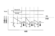
- FIG. 4 is a diagram showing a temporal change in noise current proportional to the electric charge flowing from the capacitor to the reference power supply when the switch is turned on in order from the high-order bit in each bit circuit shown in FIG. FIG.
- FIG. 5 is a diagram showing a plurality of bit circuits in which a series circuit of a switch and a current amount control element is provided between the capacitor and the reference power supply.
- FIG. 6 is a diagram showing a temporal change in noise current when the current flowing through the current amount control element is limited when the switch is turned on in order from the upper bit in the plurality of bit circuits shown in FIG.
- FIG. 7 is a diagram for explaining a problem that occurs when a constant current is applied when each switch of each bit circuit is turned on.
- FIG. 8 is a diagram showing a constant current control potential applied to the current amount control element for a certain period of time when the switch is turned on.
- FIG. 9 is a diagram showing how the establishment time becomes longer when a constant current control potential is applied to the current amount control element.
- FIG. 10 is a block diagram of a main part of the A / D conversion circuit of the second embodiment.
- FIG. 11 is a diagram showing the current control potential when the value is increased or decreased with respect to a constant value.
- FIG. 12 is a diagram showing how the establishment time is shortened when the variable current control potential shown in FIG. 11 is applied to the current amount control element.
- FIG. 13 is a diagram showing a configuration of a conventional CDAC.
- FIG. 14 is a diagram showing the configuration of each switch in the conventional CDAC.
- FIG. 15 is a diagram showing a sampling operation of the input potential when the switch of the conventional CDAC is turned on.
- FIG. 16 is a diagram showing a hold operation of the electric charge stored in the capacitor of the conventional CDAC.
- FIG. 17 is a diagram showing the results of analog / digital conversion of the conventional CDAC.
- FIG. 1 is an overall configuration diagram of the A / D conversion circuit of the first embodiment.
- the A / D conversion circuit includes an ADC overall control unit 1, a CDAC 10, a comparator 20, and a sequential comparison data generator 30.
- the ADC overall control unit 1 controls the entire ADC, and outputs the sampling control signal SCS to the switches swA1-swA4 of the CDAC10.
- the CDAC 10 samples the input potential and generates a comparative potential based on the potential held in the capacitor, the digital value, and the potential of the reference power supply Vref.
- the comparator 20 compares the comparative potential from the CDAC 10 with the reference potential Vref / 2 generated based on the reference power supply Vref, and converts the comparative potential into a digital value.
- the sequential comparison data generator 30 stores the digital value converted by the comparator 20 in a register (not shown) and outputs the digital value stored in the register to the CDAC 10 as switch signals swH and swL.
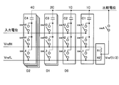
- FIG. 2 is a diagram showing a configuration of CDAC in the A / D conversion circuit of the first embodiment.
- the A / D conversion circuit is a sequential comparison type A / D conversion circuit that uses a CDAC that includes a capacitance for generating a comparison potential.
- the CDAC further provides a switch swH1-swH4 and a current amount control element QH1-QH4 between the capacitor C1-C4 and the reference power supply VrefH with respect to the CDAC shown in FIG. 13, and provides the capacitor C1-C4 and the reference power supply VrefL. It is characterized in that a switch swL1-swL4 and a current amount control element QL1-QL4 are provided between the two.
- a comparative potential is output to one end of the capacitors C2-C4, and the capacitance value increases as the lower bits of the plurality of bits go to the upper bits.
- an input potential is applied to the other end of the capacitors C1-C4.
- a bit circuit D1 including a capacitor C2, a switch swH2, a current amount control element QH2, a switch swL2, and a bit circuit D0 including a current amount control element QL2 are provided.
- the current amount control unit 11 controls the amount of current flowing through the current amount control elements QH1-QH4 and QL1-QL4.
- the current amount control elements QH1-QH4 and QL1-QL4 are made of, for example, MOSFETs.
- the current amount control elements QH1-QH4 and QL1-QL4 are also referred to as current amount control elements Q1-Q4.
- the switches swH and swL input a digital value 1 or 0 from the sequential comparison data generator 30, turn on by the digital value 1, and turn off by the digital value 0.
- the current amount control unit 11 When the current amount control unit 11 is turned on in the order of switches swH4, swH3, swH2, swH1 (switches swL4, swL3, swL2, swL1) in order from the upper bit in each bit circuit D2, D1, D0, the current amount control unit 11 is a capacitor.
- the noise current is limited to less than the permissible value by applying the current control potential to the current amount control element QH4 (QL4).
- the current amount control unit 11 turns on the current amount control element QH4 (QL4) during the period when the switches swH3, swH2 (swL3, swL2) in the bit circuits D1 and D0 excluding any of the bit circuits D2 are turned on. Do not limit the amount of current by letting it.
- FIG. 3 shows a bit circuit in which a series circuit of the capacitor C4-C2 provided between the reference power supply Vref and the comparative potential and the switch sw4-sw2 is provided bit by bit.
- FIG. 4 shows the temporal change of the noise current proportional to the electric charge flowing from the capacitors C4, C3, and C2 to the reference power supply Vref when the switches sw4, sw3, and sw2 are turned on in order from the bit circuit of the upper bit.
- the sequential comparison type A / D conversion circuit
- the CDAC is operated, the comparison potential is compared with the reference potential, and the process of determining the digital value of the next CDAC is repeated.
- the digital value is obtained from the higher-order (larger value) bit. Therefore, when considering the noise of the reference power supply, the model in which the switches sw4, sw3, and sw2 shown in FIG. 3 are turned on in order may be considered. ..
- the noise current and noise voltage are when the noise current (noise voltage) when the switch sw4 is turned on is 4, and when the switch sw3 is turned on.
- the noise current (noise voltage) of is 2, and the noise current (noise voltage) when the switch sw2 is turned on is 1. Therefore, in order to suppress noise, focus on the operation of the high-order bits.
- FIG. 4 shows the case where the allowable current is exceeded.
- the switch sw4 of the high-order bit is turned on at time t1
- the noise current flows beyond the permissible value and becomes zero at time t2.
- the potential comparison between the comparative potential and the reference potential is performed.
- the switch sw3 is turned on at time t4
- the noise current flows below the permissible value and becomes zero at time t5.
- the potential comparison between the comparative potential and the reference potential is performed.
- the switch sw2 is turned on at time t7, the noise current flows below the permissible value and becomes zero at time t8.
- the potential comparison between the comparative potential and the reference potential is performed.
- the noise current to the reference power supply Vref can be made less than the allowable value. That is, it is possible to provide an A / D conversion circuit capable of suppressing the noise voltage to a small value and reducing the error.
- the process of delaying the potential comparison time of the bit circuit is performed.
- This process has an element that slows down the conversion speed of the A / D conversion circuit.
- the conversion of all bits is not slowed down, but only the establishment time of the bit circuit with the current limit is slowed down. Therefore, in the case where the solution of the noise problem of the reference power supply is prioritized, compared with the conventional technology, This process has great advantages.
- the noise current exceeds the permissible value when the switch sw4 is turned on, and there is no problem when the switches sw3 and sw2 are turned on. It is assumed that the on-resistance of the switch sw4 is designed to suppress the current. Similar to the present invention, this design will be able to suppress the noise current (noise voltage) due to the switch sw4 in exchange for lengthening the establishment time of the bit circuit D2 when the switch sw4 is turned on.
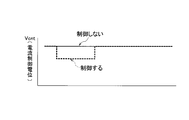
- the current amount control unit 11 limits the noise current to less than the permissible value by applying the current control potential to the current amount control element Q4 during the period when the switch sw4 is turned on.
- the current amount of the current amount control element Q4 is not limited during the period when the switches sw3 and sw2 are turned on.
- the enactment time will be increased only when the current is limited.
- the current amount control elements Q1-Q4 are used during the period from when the CDAC switch is turned on to when the CDAC starts operating and when the operation is completed. A constant current control potential was applied to suppress the current.
- the current amount control elements Q1-Q4 behave like a resistor and suppress the current. As a result, a large current does not flow, but the time at which the current ends, that is, the time for establishing the CDAC becomes long as shown in FIG.
- the problem to be solved in the second embodiment is to suppress the peak of the noise current (noise voltage)
- the relationship between the current and the time is shaped like a rectangle, and the area (charge amount) is the same.
- the height (current peak) is low.
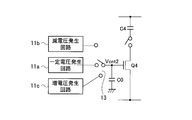
- the A / D conversion circuit of the second embodiment includes a constant voltage generation circuit 11a, a voltage reduction generation circuit 11b, a voltage increase generation circuit 11c, and a switch 13 shown in FIG.
- the constant voltage generation circuit 11a, the voltage reduction generation circuit 11b, and the voltage increase generation circuit 11c are provided in the current amount control unit 11.
- the switch 13 switches and selects the constant voltage generation circuit 11a, the voltage reduction generation circuit 11b, and the voltage increase generation circuit 11c.
- the constant voltage generation circuit 11a applies the constant current control potential Va shown in FIG. 11 to the current amount control element Q4 via the switch 13 before the time t11.
- the voltage reduction generation circuit 11b applies a current control potential Vb, which is smaller than the current control potential Va, to the current amount control element Q4 via the switch 13.
- the voltage boosting circuit 11c applies the current control potential Vc, which is larger than the current control potential Va, to the current amount control element Q4 via the switch 13.
- the establishment time when the current control potential is constant and not variably controlled is substantially the same as the establishment time when the current control potential is variably controlled. Therefore, it is possible to realize an A / D conversion circuit having a small noise current (noise voltage) without impairing the establishment time of the CDAC and therefore the conversion time of the A / D conversion circuit.
- the present invention is applicable to CDAC.
- ADC overall control unit 10 CDAC 11 Current amount control unit 20 Comparator 30 Sequential comparison data generator C1-C4 Capacitor swA0-swA4, swH1-swH4, swL1-swL4 Switch QH1-QH4, QL1-QL4 Current amount control element VrefH, VrefL Reference power supply
Abstract
In the present invention, a digital/analog converter included in an A/D conversion circuit is provided with: a plurality of bit circuits which include, so as to correspond to a plurality of bits, capacitors outputting comparative potential from one ends thereof and having capacity values increasing from lower-order bits to the higher-order bits of the plurality of bits, first switches positioned at the other ends of the capacitors and having applied thereto input potential, and series circuits comprising second switches and current amount control elements and positioned between the other ends of the capacitors and a reference power source; and a current amount control unit for controlling a current amount flowing through the current amount control elements provided to the bit circuits. In a case where the second switches are switched on, by digital values, sequentially from the higher-order bit in the respective bit circuits, and during a period in which a second switch in any one of the bit circuits that has a noise current equal to or higher than an allowable value is switched on, the noise current being proportional to electrical charge flowing from the corresponding capacitor to the reference power source, the current amount control unit regulates the noise current so to be lower than the allowable value by applying current control potential to a current amount control element in any one of the bit circuits.
Description
本発明は、逐次比較型のA/D変換回路に関する。
The present invention relates to a sequential comparison type A / D conversion circuit.
A/D変換回路として、比較電位の生成に容量を含むデジタルアナログ変換器(以下、CDACと称する)を用いた逐次比較型のA/D変換回路が知られている。CDACは、図13に示すように、1C、2C、4Cのように容量値が2nCに重み付けされたコンデンサC1-C4と、スイッチswA1-swA4,swH1-swH4,swL1-swL4、参照電源(VrefH/VrefL)、参照電源の1/2電位を生成する抵抗R1と抵抗R2とからなる直列回路とを有する。スイッチswA1-swA4,swH1-swH4,swL1-swL4は、図14に示すように、MOS-FETM1,M2とインバータIN1とからなるアナログスイッチである。
As an A / D conversion circuit, a sequential comparison type A / D conversion circuit using a digital-to-analog converter (hereinafter referred to as CDAC) including a capacitance for generating a comparative potential is known. As shown in FIG. 13, the CDAC includes a capacitor C1-C4 whose capacitance value is weighted to 2 nC such as 1C, 2C, and 4C, a switch swA1-swA4, swH1-swH4, swL1-swL4, and a reference power supply (reference power supply). VrefH / VrefL), a series circuit including a resistor R1 and a resistor R2 that generate a 1/2 potential of a reference power source. As shown in FIG. 14, the switches swA1-swA4, swH1-swH4, and swL1-swL4 are analog switches including MOS-FETs M1 and M2 and an inverter IN1.
CDACは、例えば、3ビットのビット回路D2,D1,D0を有する。入力電位をCDACに入力するためには、図15に示すスイッチswA1-swA4をオンする。入力電位を入力する動作を「サンプリング動作」と呼ぶ。この時、入力電位と比較電位とは、4C、2C、1C、1Cで示したコンデンサC4-C1を介して接続される。コンデンサC4-C1には、入力電位と比較電位との差による電荷が蓄積される。
The CDAC has, for example, 3-bit bit circuits D2, D1, D0. In order to input the input potential to the CDAC, the switches swA1-swA4 shown in FIG. 15 are turned on. The operation of inputting the input potential is called "sampling operation". At this time, the input potential and the comparative potential are connected via the capacitors C4-C1 shown by 4C, 2C, 1C and 1C. Charges due to the difference between the input potential and the comparative potential are accumulated in the capacitors C4-C1.
コンデンサC4-C1に蓄積された電荷により、スイッチswA1-swA4をオフしても、図16に太い実線で示すノードの電位は保存される。この動作を「ホールド動作」と呼ぶ。
Due to the electric charge accumulated in the capacitors C4-C1, even if the switches swA1-swA4 are turned off, the potential of the node shown by the thick solid line in FIG. 16 is preserved. This operation is called a "hold operation".
次に、図17に示すように、ビット回路D2,D1,D0のそれぞれに設置したスイッチswH1-swH3をオフし、スイッチswH4をオンする。また、スイッチswL1-swL3をオンし、スイッチswL4をオフする。コンデンサC1-C4に参照電源VrefH又はVrefLを印加した時の比較電位を観測する。
Next, as shown in FIG. 17, the switches swH1-swH3 installed in each of the bit circuits D2, D1 and D0 are turned off, and the switch swH4 is turned on. Also, the switch swL1-swL3 is turned on and the switch swL4 is turned off. Observe the comparative potential when the reference power supply VrefH or VrefL is applied to the capacitors C1-C4.
スイッチのオンの組み合わせを試し、比較電位がサンプリング動作時の参照電源の1/2電位と一致するスイッチの組み合わせを検索する。比較器が、例えば、ビット回路D2のスイッチswH、ビット回路D1,D0のスイッチswLをオンした時に、比較電位を参照電源Vrefの1/2電位である基準電位と比較する。比較電位が参照電源Vrefの1/2電位である基準電位となった場合、比較器は、入力電位に対応するデジタル値は100(2進数)である。即ち、ビット回路D2が「1」、ビット回路D1が「0」、ビット回路D0が「0」を出力する。これがA/D変換回路の変換結果である。
Try the switch on combination and search for the switch combination whose comparative potential matches the 1/2 potential of the reference power supply during sampling operation. When the comparator turns on, for example, the switch swH of the bit circuit D2 and the switch swL of the bit circuits D1 and D0, the comparison potential is compared with the reference potential which is 1/2 potential of the reference power supply Vref. When the comparative potential becomes the reference potential which is 1/2 potential of the reference power supply Vref, the comparator has a digital value of 100 (binary) corresponding to the input potential. That is, the bit circuit D2 outputs "1", the bit circuit D1 outputs "0", and the bit circuit D0 outputs "0". This is the conversion result of the A / D conversion circuit.
このようなA/D変換回路の誤差を小さくするためには、CDACの出力電位の誤差を小さくする必要がある。CDACの出力電位の誤差を小さくするためには、参照電源VrefH,VrefLの電位が意図した正しい電位である必要がある。CDACは、動作時に、参照電源にノイズ電流を注入する構造になっている。参照電源にノイズ電流を注入すると、参照電源には 参照電源が持つインピーダンス ×ノイズ電流 =ノイズ電圧のずれが生じる。このため、A/D変換回路に誤差をもたらす。
In order to reduce the error of such an A / D conversion circuit, it is necessary to reduce the error of the output potential of the CDAC. In order to reduce the error of the output potential of the CDAC, the potentials of the reference power supplies VrefH and VrefL need to be the intended correct potentials. The CDAC has a structure in which a noise current is injected into the reference power supply during operation. When a noise current is injected into the reference power supply, the impedance of the reference power supply x noise current = noise voltage shift occurs in the reference power supply. Therefore, an error is caused in the A / D conversion circuit.
本発明の課題は、ノイズ電圧を小さく抑え、誤差を小さくすることができるA/D変換回路を提供することである。
An object of the present invention is to provide an A / D conversion circuit capable of suppressing the noise voltage and reducing the error.
前記課題を解決するために、本発明のA/D変換回路は、入力電位をサンプリング・ホールドした電位とデジタル値と参照電源とに基づき比較電位を生成するデジタル/アナログ変換器を備え、前記比較電位を前記参照電源に基づき生成された基準電位と比較し前記比較電位を前記デジタル値に変換し、変換された前記デジタル値を前記デジタル/アナログ変換器に出力するA/D変換回路である。
In order to solve the above problems, the A / D conversion circuit of the present invention includes a digital / analog converter that generates a comparative potential based on the potential obtained by sampling and holding the input potential, the digital value, and the reference power supply, and the comparison is performed. It is an A / D conversion circuit that compares a potential with a reference potential generated based on the reference power source, converts the comparative potential into the digital value, and outputs the converted digital value to the digital / analog converter.
前記デジタル/アナログ変換器は、一端に前記比較電位が出力され複数ビットの下位ビットから上位ビットに行くに従って容量値が大きくなるコンデンサ、前記コンデンサの他端に前記入力電位が印加される第1スイッチ、前記コンデンサの他端と前記参照電源との間に第2スイッチと電流量制御素子との直列回路が前記複数ビットに対応して設けられた複数のビット回路と、前記複数のビット回路の各ビット回路に設けられた前記電流量制御素子に流れる電流量を制御する電流量制御部とを備え、前記電流量制御部は、前記デジタル値により各ビット回路において上位ビットから順に前記第2スイッチがオンされる場合に、前記コンデンサから前記参照電源に流れ込む電荷に比例するノイズ電流が許容値以上になるいずれかの前記ビット回路内の前記第2スイッチがオンとなる期間には、前記いずれかの前記ビット回路内の前記電流量制御素子に電流制御電位を印加することで前記ノイズ電流を許容値未満に制限する。
The digital / analog converter is a capacitor in which the comparative current is output at one end and the capacitance value increases from the lower bits of a plurality of bits to the upper bits, and the first switch in which the input current is applied to the other end of the capacitor. A plurality of bit circuits in which a series circuit of a second switch and a current amount control element is provided between the other end of the capacitor and the reference power supply corresponding to the plurality of bits, and each of the plurality of bit circuits. A current amount control unit for controlling the amount of current flowing through the current amount control element provided in the bit circuit is provided, and the current amount control unit has the second switch in order from the upper bit in each bit circuit according to the digital value. When the second switch in any of the bit circuits is turned on, the noise current proportional to the charge flowing from the capacitor to the reference power supply becomes equal to or more than an allowable value. By applying a current control potential to the current amount control element in the bit circuit, the noise current is limited to less than an allowable value.
本発明によれば、デジタル値により各ビット回路において上位ビットから順に第2スイッチがオンされる場合に、ノイズ電流が許容値以上になるいずれかのビット回路内の第2スイッチがオンとなる期間に、いずれかのビット回路内の電流量制御素子に電流制御電位を印加することでノイズ電流を許容値未満に制限する。
According to the present invention, when the second switch is turned on in order from the upper bit in each bit circuit by a digital value, the period during which the second switch in any of the bit circuits where the noise current becomes equal to or higher than the allowable value is turned on. In addition, the noise current is limited to less than the permissible value by applying a current control potential to the current amount control element in any of the bit circuits.
これにより、参照電源へのノイズ電流を許容値未満にすることができる。即ち、ノイズ電圧を小さく抑え、誤差を小さくすることができるA/D変換回路を提供することができる。
As a result, the noise current to the reference power supply can be made less than the allowable value. That is, it is possible to provide an A / D conversion circuit capable of suppressing the noise voltage to a small value and reducing the error.
以下、実施形態のA/D変換回路を図面を参照しながら説明する。
Hereinafter, the A / D conversion circuit of the embodiment will be described with reference to the drawings.
(第1の実施形態)
図1は第1の実施形態のA/D変換回路の全体構成図である。A/D変換回路は、ADC全体制御部1、CDAC10、コンパレータ20、逐次型比較データ生成器30を備えている。 (First Embodiment)
FIG. 1 is an overall configuration diagram of the A / D conversion circuit of the first embodiment. The A / D conversion circuit includes an ADC overall control unit 1, aCDAC 10, a comparator 20, and a sequential comparison data generator 30.
図1は第1の実施形態のA/D変換回路の全体構成図である。A/D変換回路は、ADC全体制御部1、CDAC10、コンパレータ20、逐次型比較データ生成器30を備えている。 (First Embodiment)
FIG. 1 is an overall configuration diagram of the A / D conversion circuit of the first embodiment. The A / D conversion circuit includes an ADC overall control unit 1, a
ADC全体制御部1は、ADCの全体を制御するもので、サンプリング制御信号SCSをCDAC10のスイッチswA1-swA4に出力する。CDAC10は、入力電位をサンプリングしコンデンサにホールドした電位とデジタル値と参照電源Vrefの電位に基づいて比較電位を生成する。
The ADC overall control unit 1 controls the entire ADC, and outputs the sampling control signal SCS to the switches swA1-swA4 of the CDAC10. The CDAC 10 samples the input potential and generates a comparative potential based on the potential held in the capacitor, the digital value, and the potential of the reference power supply Vref.
コンパレータ20は、CDAC10からの比較電位と参照電源Vrefに基づいて生成された基準電位Vref/2を比較し比較電位をデジタル値に変換する。逐次型比較データ生成器30は、コンパレータ20で変換されたデジタル値を図示しないレジスタに記憶するとともにレジスタに記憶されたデジタル値をスイッチ信号swH,swLとしてCDAC10に出力する。
The comparator 20 compares the comparative potential from the CDAC 10 with the reference potential Vref / 2 generated based on the reference power supply Vref, and converts the comparative potential into a digital value. The sequential comparison data generator 30 stores the digital value converted by the comparator 20 in a register (not shown) and outputs the digital value stored in the register to the CDAC 10 as switch signals swH and swL.
図2は第1の実施の形態のA/D変換回路内のCDACの構成を示す図である。A/D変換回路は、比較電位の生成に容量を含むCDACを用いた逐次比較型のA/D変換回路である。
FIG. 2 is a diagram showing a configuration of CDAC in the A / D conversion circuit of the first embodiment. The A / D conversion circuit is a sequential comparison type A / D conversion circuit that uses a CDAC that includes a capacitance for generating a comparison potential.
CDACは、図13に示すCDACに対して、さらに、コンデンサC1-C4と参照電源VrefHとの間にスイッチswH1-swH4と電流量制御素子QH1-QH4とを設け、コンデンサC1-C4と参照電源VrefLとの間にスイッチswL1-swL4と電流量制御素子QL1-QL4とを設けていることを特徴とする。
The CDAC further provides a switch swH1-swH4 and a current amount control element QH1-QH4 between the capacitor C1-C4 and the reference power supply VrefH with respect to the CDAC shown in FIG. 13, and provides the capacitor C1-C4 and the reference power supply VrefL. It is characterized in that a switch swL1-swL4 and a current amount control element QL1-QL4 are provided between the two.
コンデンサC2-C4は、一端に比較電位が出力され複数ビットの下位ビットから上位ビットに行くに従って容量値が大きくなる。スイッチswA1-swA4は、コンデンサC1-C4の他端に入力電位が印加される。
A comparative potential is output to one end of the capacitors C2-C4, and the capacitance value increases as the lower bits of the plurality of bits go to the upper bits. In the switches swA1-swA4, an input potential is applied to the other end of the capacitors C1-C4.
コンデンサC4とスイッチswH4と電流量制御素子QH4とスイッチswL4と電流量制御素子QL4とを含むビット回路D2と、コンデンサC3とスイッチswH3と電流量制御素子QH3とスイッチswL3と電流量制御素子QL3とを含むビット回路D1と、コンデンサC2とスイッチswH2と電流量制御素子QH2とスイッチswL2と電流量制御素子QL2とを含むビット回路D0とが設けられている。
A bit circuit D2 including a capacitor C4, a switch swH4, a current amount control element QH4, a switch swL4, and a current amount control element QL4, a capacitor C3, a switch swH3, a current amount control element QH3, a switch swL3, and a current amount control element QL3. A bit circuit D1 including a capacitor C2, a switch swH2, a current amount control element QH2, a switch swL2, and a bit circuit D0 including a current amount control element QL2 are provided.
電流量制御部11は、電流量制御素子QH1-QH4,QL1-QL4に流れる電流量を制御する。電流量制御素子QH1-QH4,QL1-QL4は、例えば、MOSFETからなる。電流量制御素子QH1-QH4, QL1-QL4は、電流量制御素子Q1-Q4とも称する。
The current amount control unit 11 controls the amount of current flowing through the current amount control elements QH1-QH4 and QL1-QL4. The current amount control elements QH1-QH4 and QL1-QL4 are made of, for example, MOSFETs. The current amount control elements QH1-QH4 and QL1-QL4 are also referred to as current amount control elements Q1-Q4.
スイッチswH,swLは、逐次型比較データ生成器30からデジタル値1又は0を入力し、デジタル値1によりオンし、デジタル値0によりオフする。
The switches swH and swL input a digital value 1 or 0 from the sequential comparison data generator 30, turn on by the digital value 1, and turn off by the digital value 0.
電流量制御部11は、各ビット回路D2,D1,D0において上位ビットから順にスイッチswH4、swH3、swH2、swH1の順(スイッチswL4、swL3、swL2、swL1の順)でオンされる場合に、コンデンサC4、C3、C2、C1から参照電源VrefH(VrefL)に流れ込む電荷に比例するノイズ電流が許容値以上になるいずれかのビット回路、例えばビット回路D2内のスイッチswH4(swL4)がオンとなる期間に、電流量制御素子QH4(QL4)に電流制御電位を印加することでノイズ電流を許容値未満に制限する。
When the current amount control unit 11 is turned on in the order of switches swH4, swH3, swH2, swH1 (switches swL4, swL3, swL2, swL1) in order from the upper bit in each bit circuit D2, D1, D0, the current amount control unit 11 is a capacitor. The period during which any bit circuit, for example, the switch swH4 (swL4) in the bit circuit D2 is turned on, in which the noise current proportional to the electric charge flowing from the reference power supply VrefH (VrefL) from C4, C3, C2, C1 becomes equal to or higher than the allowable value. In addition, the noise current is limited to less than the permissible value by applying the current control potential to the current amount control element QH4 (QL4).
また、電流量制御部11は、いずれかのビット回路D2を除くビット回路D1,D0内のスイッチswH3,swH2(swL3,swL2)がオンとなる期間に、電流量制御素子QH4(QL4)をオンさせることで電流量を制限しないようにする。
Further, the current amount control unit 11 turns on the current amount control element QH4 (QL4) during the period when the switches swH3, swH2 (swL3, swL2) in the bit circuits D1 and D0 excluding any of the bit circuits D2 are turned on. Do not limit the amount of current by letting it.
図3に参照電源Vrefと比較電位との間に設けられたコンデンサC4-C2とスイッチsw4-sw2との直列回路をビット毎に設けたビット回路を示す。図4に上位ビットのビット回路から順にスイッチsw4、sw3、sw2をオンした時にコンデンサC4、C3、C2から参照電源Vrefに流れ込む電荷に比例するノイズ電流の時間的な変化を示す。
FIG. 3 shows a bit circuit in which a series circuit of the capacitor C4-C2 provided between the reference power supply Vref and the comparative potential and the switch sw4-sw2 is provided bit by bit. FIG. 4 shows the temporal change of the noise current proportional to the electric charge flowing from the capacitors C4, C3, and C2 to the reference power supply Vref when the switches sw4, sw3, and sw2 are turned on in order from the bit circuit of the upper bit.
逐次比較型A/D変換回路の動作は、まず、CDACを動作させ、比較電位を基準電位と比較し、次のCDACのデジタル値を決める処理を繰返し行う。逐次比較型では、デジタル値を上位(値の大きい)のビットから求めて行くので、参照電源のノイズを考える場合に、図3に示すスイッチsw4、sw3、sw2を順にオンするモデルで考えれば良い。
In the operation of the sequential comparison type A / D conversion circuit, first, the CDAC is operated, the comparison potential is compared with the reference potential, and the process of determining the digital value of the next CDAC is repeated. In the sequential comparison type, the digital value is obtained from the higher-order (larger value) bit. Therefore, when considering the noise of the reference power supply, the model in which the switches sw4, sw3, and sw2 shown in FIG. 3 are turned on in order may be considered. ..
スイッチsw4、sw3、sw2を順にオンすると、コンデンサC4、C3、C2から4C、2C、1Cの電荷が参照電源Vrefに流れ込む。CDACのワースト・モデルでは、4C、2C、1Cの電荷量は4:2:1である。
When the switches sw4, sw3, and sw2 are turned on in order, the charges of the capacitors C4, C3, C2 to 4C, 2C, and 1C flow into the reference power supply Vref. In the worst model of CDAC, the charge amounts of 4C, 2C and 1C are 4: 2: 1.
参照電源Vrefに流れ込む電荷量とノイズ電流が比例関係にあるならば、ノイズ電流、ノイズ電圧は、スイッチsw4をオンした時のノイズ電流(ノイズ電圧)は4である時、スイッチsw3をオンした時のノイズ電流(ノイズ電圧)は2であり、スイッチsw2をオンした時のノイズ電流(ノイズ電圧)は1である。従って、ノイズを抑制するには、上位ビットの動作に着目する。
If the amount of charge flowing into the reference power supply Vref and the noise current are in a proportional relationship, the noise current and noise voltage are when the noise current (noise voltage) when the switch sw4 is turned on is 4, and when the switch sw3 is turned on. The noise current (noise voltage) of is 2, and the noise current (noise voltage) when the switch sw2 is turned on is 1. Therefore, in order to suppress noise, focus on the operation of the high-order bits.
図4では、許容電流を超えている場合を示している。時刻t1に、上位ビットのスイッチsw4をオンさせると、ノイズ電流が許容値を超えて流れ、時刻t2でゼロになる。時刻t3で比較電位と基準電位との電位比較を行う。時刻t4に、スイッチsw3をオンさせると、ノイズ電流が許容値以下で流れ、時刻t5でゼロになる。
FIG. 4 shows the case where the allowable current is exceeded. When the switch sw4 of the high-order bit is turned on at time t1, the noise current flows beyond the permissible value and becomes zero at time t2. At time t3, the potential comparison between the comparative potential and the reference potential is performed. When the switch sw3 is turned on at time t4, the noise current flows below the permissible value and becomes zero at time t5.
時刻t6で比較電位と基準電位との電位比較を行う。時刻t7に、スイッチsw2をオンさせると、ノイズ電流が許容値以下で流れ、時刻t8でゼロになる。時刻t9で比較電位と基準電位との電位比較を行う。
At time t6, the potential comparison between the comparative potential and the reference potential is performed. When the switch sw2 is turned on at time t7, the noise current flows below the permissible value and becomes zero at time t8. At time t9, the potential comparison between the comparative potential and the reference potential is performed.
このように、上位ビットのスイッチsw4をオンさせると、ノイズ電流が許容値を超えるため、ノイズ誤差が大きくなる。このため、図5に示すようにスイッチsw4、sw3、sw2と参照電源Vrefとの間に電流量制御素子Q4、Q3、Q2を設けている。
In this way, when the switch sw4 of the high-order bit is turned on, the noise current exceeds the permissible value, so that the noise error becomes large. Therefore, as shown in FIG. 5, current amount control elements Q4, Q3, and Q2 are provided between the switches sw4, sw3, and sw2 and the reference power supply Vref.
電流量制御部11は、図5に示すように、上位ビットから順にスイッチsw4、sw3、sw2の順でオンされる場合に、コンデンサC4、C3、C2から参照電源Vrefに流れ込む電荷に比例するノイズ電流が許容値以上になるビット回路D2内のスイッチsw4がオンとなる期間(図6に示す時刻t11-t13)に、電流量制御素子Q4に電流制御電位を印加することでコンデンサC4からのノイズ電流を許容値未満に制限する。
As shown in FIG. 5, when the current amount control unit 11 is turned on in the order of the switches sw4, sw3, and sw2 in order from the upper bit, the noise proportional to the electric charge flowing from the capacitors C4, C3, and C2 to the reference power supply Vref. Noise from the capacitor C4 by applying the current control potential to the current amount control element Q4 during the period when the switch sw4 in the bit circuit D2 where the current becomes equal to or higher than the allowable value is turned on (time t11-t13 shown in FIG. 6). Limit the current below the permissible value.
これにより、参照電源Vrefへのノイズ電流を許容値未満にすることができる。即ち、ノイズ電圧を小さく抑え、誤差を小さくすることができるA/D変換回路を提供することができる。
As a result, the noise current to the reference power supply Vref can be made less than the allowable value. That is, it is possible to provide an A / D conversion circuit capable of suppressing the noise voltage to a small value and reducing the error.
また、電流の制限を与えたビット回路D2の制定時間(正しい電位を出力するのに要する時間t12-t13)が大きくなるので、当該ビット回路の電位比較時刻を遅らせる処理を行なう。この処理にはA/D変換回路の変換速度を遅くする要素がある。しかし、全てのビットの変換が遅くなるのではなく、電流制限を与えたビット回路の制定時間のみが遅いので、参照電源のノイズの問題の解決が優先されるケースにおいて、従来技術に比べて、この処理には大きな利点がある。
Further, since the establishment time of the bit circuit D2 to which the current is limited (the time t12-t13 required to output the correct potential) becomes large, the process of delaying the potential comparison time of the bit circuit is performed. This process has an element that slows down the conversion speed of the A / D conversion circuit. However, the conversion of all bits is not slowed down, but only the establishment time of the bit circuit with the current limit is slowed down. Therefore, in the case where the solution of the noise problem of the reference power supply is prioritized, compared with the conventional technology, This process has great advantages.
なお、電流の制限を当該ビットの切り替え期間で当該ビットの電流のみとした理由について、以下に説明する。CDACの各スイッチをオンさせるときに、一定の電流しか流れないようにしたスイッチsw4、sw3、sw2を設置すれば、本発明と同じ効果を持つと思われるかもしれない。
The reason why the current limit is limited to the current of the bit during the bit switching period will be described below. If switches sw4, sw3, and sw2 are installed so that only a constant current flows when each switch of the CDAC is turned on, it may be considered that the same effect as that of the present invention is obtained.
仮に、スイッチsw4をオンした時にノイズ電流(ノイズ電圧)が許容値を超え、スイッチsw3、sw2をオンしたときには問題がないケースを考える。スイッチsw4のオン抵抗が電流を抑制する値に設計したとする。この設計は、本発明と同様に、スイッチsw4をオンしたとき、ビット回路D2の制定時間を長くするのと引き換えにスイッチsw4によるノイズ電流(ノイズ電圧)を抑制することができるだろう。
Suppose that the noise current (noise voltage) exceeds the permissible value when the switch sw4 is turned on, and there is no problem when the switches sw3 and sw2 are turned on. It is assumed that the on-resistance of the switch sw4 is designed to suppress the current. Similar to the present invention, this design will be able to suppress the noise current (noise voltage) due to the switch sw4 in exchange for lengthening the establishment time of the bit circuit D2 when the switch sw4 is turned on.
しかし、この設計には問題がある。図7に示すように、スイッチsw4のオン抵抗Rが大きいと、スイッチsw3又はスイッチsw2をオンオフする時にも制定時間が大きくなる。
However, there is a problem with this design. As shown in FIG. 7, if the on-resistance R of the switch sw4 is large, the establishment time becomes long even when the switch sw3 or the switch sw2 is turned on and off.
図7において、スイッチsw3をオンして比較電位を下げるケースにおいて、本来、コンデンサC4の一端が参照電位であるべきであるが、大きな抵抗Rの存在により一時的に参照電位を超えた電位になる。このため、比較電位も一時的に誤った値になる。これは、参照電位からコンデンサC4の一端に電荷が注入されることで解消するが、抵抗Rが大きいと解消するのに時間がかかる。
In FIG. 7, in the case where the switch sw3 is turned on to lower the comparative potential, one end of the capacitor C4 should be the reference potential, but due to the presence of the large resistor R, the potential temporarily exceeds the reference potential. .. Therefore, the comparative potential also temporarily becomes an erroneous value. This is solved by injecting an electric charge from the reference potential to one end of the capacitor C4, but it takes time to solve the problem when the resistance R is large.
従って、ノイズ電流(ノイズ電圧)を抑制する目的でスイッチsw4のオン抵抗を大きくすることは、スイッチsw3、スイッチsw2の切り替え時の制定時間を大きくする。
Therefore, increasing the on-resistance of the switch sw4 for the purpose of suppressing the noise current (noise voltage) increases the establishment time when switching between the switch sw3 and the switch sw2.
このため、第1の実施形態では、電流量制御部11は、スイッチsw4がオンとなる期間に、電流量制御素子Q4に電流制御電位を印加することでノイズ電流を許容値未満に制限し、スイッチsw3,sw2がオンとなる期間に、電流量制御素子Q4の電流量を制限しない。
Therefore, in the first embodiment, the current amount control unit 11 limits the noise current to less than the permissible value by applying the current control potential to the current amount control element Q4 during the period when the switch sw4 is turned on. The current amount of the current amount control element Q4 is not limited during the period when the switches sw3 and sw2 are turned on.
これにより、制定時間が大きくなるのは、電流を制限した時に限定される。電流を制限しない時に制定時間に影響を与えないようにすることで、従来技術よりも速い変換時間と小さいノイズとを両立したA/D変換回路を提供することができる。
As a result, the enactment time will be increased only when the current is limited. By not affecting the establishment time when the current is not limited, it is possible to provide an A / D conversion circuit that achieves both faster conversion time and smaller noise than in the prior art.
(第2の実施形態)
第1の実施形態のA/D変換回路では、CDACのスイッチをオンしてCDACが動作を開始し、動作を完了するまでの期間、図8に示すように、電流量制御素子Q1-Q4に一定の電流制御電位を印加して、電流を抑制した。 (Second Embodiment)
In the A / D conversion circuit of the first embodiment, as shown in FIG. 8, the current amount control elements Q1-Q4 are used during the period from when the CDAC switch is turned on to when the CDAC starts operating and when the operation is completed. A constant current control potential was applied to suppress the current.
この場合、電流量制御素子Q1-Q4は、抵抗のように振る舞い、電流を抑制する。その結果、大きな電流は流れないが、流れ終わる時間、即ち、図9に示すように、CDACの制定時間は長くなる。
In this case, the current amount control elements Q1-Q4 behave like a resistor and suppress the current. As a result, a large current does not flow, but the time at which the current ends, that is, the time for establishing the CDAC becomes long as shown in FIG.
電流量制御素子Q1-Q4がオンしてから抵抗のように振る舞う場合、電流と時間の関係は、図6に示すように、直角三角形のような形になる。
When the current amount control element Q1-Q4 behaves like a resistor after it is turned on, the relationship between the current and time becomes like a right triangle as shown in FIG.
第2の実施の形態で解決したい課題は、ノイズ電流(ノイズ電圧)のピークを抑制することであるので、電流と時間との関係を長方形のような形にして、面積(電荷量)は同じであるが、高さ(電流のピーク)が低いのが望ましい。
Since the problem to be solved in the second embodiment is to suppress the peak of the noise current (noise voltage), the relationship between the current and the time is shaped like a rectangle, and the area (charge amount) is the same. However, it is desirable that the height (current peak) is low.
前記課題を解決するために、第2の実施形態のA/D変換回路は、図10に示す一定電圧発生回路11a、減電圧発生回路11b、増電圧発生回路11c、スイッチ13を備えている。一定電圧発生回路11a、減電圧発生回路11b、増電圧発生回路11cは、電流量制御部11内に設けられる。スイッチ13は、一定電圧発生回路11a、減電圧発生回路11b、増電圧発生回路11cを切り替え選択する。
In order to solve the above problems, the A / D conversion circuit of the second embodiment includes a constant voltage generation circuit 11a, a voltage reduction generation circuit 11b, a voltage increase generation circuit 11c, and a switch 13 shown in FIG. The constant voltage generation circuit 11a, the voltage reduction generation circuit 11b, and the voltage increase generation circuit 11c are provided in the current amount control unit 11. The switch 13 switches and selects the constant voltage generation circuit 11a, the voltage reduction generation circuit 11b, and the voltage increase generation circuit 11c.
次に、図6に示す直角三角形をなしたノイズ電流に対して、図11に示す電流制御電位を電流量制御素子に印加したときにノイズ電流のピークが低くなることを説明する。
Next, it will be described that the peak of the noise current becomes lower when the current control potential shown in FIG. 11 is applied to the current amount control element with respect to the noise current having a right triangle shape shown in FIG.
まず、一定電圧発生回路11aは、時刻t11前に、図11に示す一定の電流制御電位Vaをスイッチ13を介して電流量制御素子Q4に印加する。次に、時刻t11に、減電圧発生回路11bは、電流制御電位Vaよりも減少した電流制御電位Vbをスイッチ13を介して電流量制御素子Q4に印加する。
First, the constant voltage generation circuit 11a applies the constant current control potential Va shown in FIG. 11 to the current amount control element Q4 via the switch 13 before the time t11. Next, at time t11, the voltage reduction generation circuit 11b applies a current control potential Vb, which is smaller than the current control potential Va, to the current amount control element Q4 via the switch 13.
次に、時刻t12に、増電圧発生回路11cは、電流制御電位Vaよりも増加した電流制御電位Vcをスイッチ13を介して電流量制御素子Q4に印加する。
Next, at time t12, the voltage boosting circuit 11c applies the current control potential Vc, which is larger than the current control potential Va, to the current amount control element Q4 via the switch 13.
このため、電流と時間との関係が長方形のような形になり、面積(電荷量)は同じであるが、高さ(電流のピーク)が低くなる。
For this reason, the relationship between current and time becomes like a rectangle, and the area (charge amount) is the same, but the height (current peak) is low.
これにより、図12に示すように、電流制御電位を一定にして可変制御しない場合の制定時間と、電流制御電位を可変制御する場合の制定時間とが略同じとなる。従って、CDACの制定時間、よって、A/D変換回路の変換時間を損なうことなく、ノイズ電流(ノイズ電圧)の小さいA/D変換回路を実現することができる。
As a result, as shown in FIG. 12, the establishment time when the current control potential is constant and not variably controlled is substantially the same as the establishment time when the current control potential is variably controlled. Therefore, it is possible to realize an A / D conversion circuit having a small noise current (noise voltage) without impairing the establishment time of the CDAC and therefore the conversion time of the A / D conversion circuit.
本発明は、CDACに適用可能である。
The present invention is applicable to CDAC.
1 ADC全体制御部
10 CDAC
11 電流量制御部
20 コンパレータ
30 逐次型比較データ生成器
C1-C4 コンデンサ
swA0-swA4,swH1-swH4,swL1-swL4 スイッチ
QH1-QH4,QL1-QL4 電流量制御素子
VrefH,VrefL 参照電源 1 ADCoverall control unit 10 CDAC
11 Currentamount control unit 20 Comparator 30 Sequential comparison data generator C1-C4 Capacitor swA0-swA4, swH1-swH4, swL1-swL4 Switch QH1-QH4, QL1-QL4 Current amount control element VrefH, VrefL Reference power supply
10 CDAC
11 電流量制御部
20 コンパレータ
30 逐次型比較データ生成器
C1-C4 コンデンサ
swA0-swA4,swH1-swH4,swL1-swL4 スイッチ
QH1-QH4,QL1-QL4 電流量制御素子
VrefH,VrefL 参照電源 1 ADC
11 Current
Claims (4)
- 入力電位をサンプリング・ホールドした電位とデジタル値と参照電源とに基づき比較電位を生成するデジタル/アナログ変換器を備え、前記比較電位を前記参照電源に基づき生成された基準電位と比較し前記比較電位を前記デジタル値に変換し、変換された前記デジタル値を前記デジタル/アナログ変換器に出力するA/D変換回路であって、
前記デジタル/アナログ変換器は、一端に前記比較電位が出力され複数ビットの下位ビットから上位ビットに行くに従って容量値が大きくなるコンデンサ、前記コンデンサの他端に前記入力電位が印加される第1スイッチ、前記コンデンサの他端と前記参照電源との間に第2スイッチと電流量制御素子との直列回路が前記複数ビットに対応して設けられた複数のビット回路と、
前記複数のビット回路の各ビット回路に設けられた前記電流量制御素子に流れる電流量を制御する電流量制御部とを備え、
前記電流量制御部は、前記デジタル値により各ビット回路において上位ビットから順に前記第2スイッチがオンされる場合に、前記コンデンサから前記参照電源に流れ込む電荷に比例するノイズ電流が許容値以上になるいずれかの前記ビット回路内の前記第2スイッチがオンとなる期間に前記いずれかの前記ビット回路内の前記電流量制御素子に電流制御電位を印加することで前記ノイズ電流を許容値未満に制限するA/D変換回路。 A digital / analog converter that generates a comparative potential based on a potential obtained by sampling and holding an input potential, a digital value, and a reference power source is provided, and the comparative potential is compared with a reference potential generated based on the reference power source. Is an A / D conversion circuit that converts the converted digital value into the digital value and outputs the converted digital value to the digital / analog converter.
The digital / analog converter is a capacitor in which the comparative potential is output at one end and the capacitance value increases from the lower bits of a plurality of bits to the upper bits, and the first switch in which the input potential is applied to the other end of the capacitor. A plurality of bit circuits in which a series circuit of the second switch and the current amount control element is provided between the other end of the capacitor and the reference power supply corresponding to the plurality of bits.
A current amount control unit for controlling the amount of current flowing through the current amount control element provided in each bit circuit of the plurality of bit circuits is provided.
In the current amount control unit, when the second switch is turned on in order from the upper bit in each bit circuit by the digital value, the noise current proportional to the electric charge flowing from the capacitor to the reference power supply becomes equal to or more than the allowable value. The noise current is limited to less than the permissible value by applying a current control potential to the current amount control element in any of the bit circuits during the period when the second switch in the bit circuit is turned on. A / D conversion circuit. - 前記電流量制御部は、前記いずれかの前記ビット回路を除くビット回路内の前記第2スイッチがオンとなる期間に前記いずれかの前記ビット回路内の前記電流量制御素子の電流量を制限しない請求項1記載のA/D変換回路。 The current amount control unit does not limit the current amount of the current amount control element in any of the bit circuits during the period when the second switch in the bit circuit other than the one of the bit circuits is turned on. The A / D conversion circuit according to claim 1.
- 前記電流量制御部は、前記電流制御電位として前記ノイズ電流と時間との関係が長方形になるような電位を前記電流量制御素子に印加する請求項1又は2記載のA/D変換回路。 The A / D conversion circuit according to claim 1 or 2, wherein the current amount control unit applies a potential as the current control potential such that the relationship between the noise current and time becomes rectangular to the current amount control element.
- 前記電流量制御部は、前記電流制御電位として一定の電流制御電位よりも減少した電流制御電位を前記電流量制御素子に印加した後、前記一定の電流制御電位よりも増加した電流制御電位を前記電流量制御素子に印加する請求項3記載のA/D変換回路。 The current amount control unit applies a current control potential that is smaller than a constant current control potential as the current control potential to the current amount control element, and then applies a current control potential that is greater than the constant current control potential. The A / D conversion circuit according to claim 3, which is applied to a current amount control element.
Priority Applications (4)
| Application Number | Priority Date | Filing Date | Title |
|---|---|---|---|
| CN201980097912.6A CN114128151A (en) | 2019-07-05 | 2019-07-05 | A/D conversion circuit |
| JP2021530353A JP7380688B2 (en) | 2019-07-05 | 2019-07-05 | A/D conversion circuit |
| PCT/JP2019/026856 WO2021005654A1 (en) | 2019-07-05 | 2019-07-05 | A/d conversion circuit |
| US17/563,109 US11689211B2 (en) | 2019-07-05 | 2021-12-28 | Analog-to-digital converter |
Applications Claiming Priority (1)
| Application Number | Priority Date | Filing Date | Title |
|---|---|---|---|
| PCT/JP2019/026856 WO2021005654A1 (en) | 2019-07-05 | 2019-07-05 | A/d conversion circuit |
Related Child Applications (1)
| Application Number | Title | Priority Date | Filing Date |
|---|---|---|---|
| US17/563,109 Continuation US11689211B2 (en) | 2019-07-05 | 2021-12-28 | Analog-to-digital converter |
Publications (1)
| Publication Number | Publication Date |
|---|---|
| WO2021005654A1 true WO2021005654A1 (en) | 2021-01-14 |
Family
ID=74113948
Family Applications (1)
| Application Number | Title | Priority Date | Filing Date |
|---|---|---|---|
| PCT/JP2019/026856 WO2021005654A1 (en) | 2019-07-05 | 2019-07-05 | A/d conversion circuit |
Country Status (4)
| Country | Link |
|---|---|
| US (1) | US11689211B2 (en) |
| JP (1) | JP7380688B2 (en) |
| CN (1) | CN114128151A (en) |
| WO (1) | WO2021005654A1 (en) |
Citations (4)
| Publication number | Priority date | Publication date | Assignee | Title |
|---|---|---|---|---|
| JP2002374169A (en) * | 2001-06-13 | 2002-12-26 | Matsushita Electric Ind Co Ltd | Successive comparison type a/d converter |
| JP2005295315A (en) * | 2004-04-01 | 2005-10-20 | Oki Electric Ind Co Ltd | Successive comparison a/d converter and comparator |
| US20100271245A1 (en) * | 2009-04-27 | 2010-10-28 | Linear Technology Corporation | Complex-admittance digital-to-analog converter |
| US20190068179A1 (en) * | 2017-08-29 | 2019-02-28 | Realtek Semiconductor Corporation | Data converter and impedance matching control method thereof |
Family Cites Families (14)
| Publication number | Priority date | Publication date | Assignee | Title |
|---|---|---|---|---|
| US4200863A (en) * | 1977-10-03 | 1980-04-29 | The Regents Of The University Of California | Weighted capacitor analog/digital converting apparatus and method |
| US4350975A (en) * | 1980-07-18 | 1982-09-21 | American Microsystems, Inc. | Dual bandwidth autozero loop for a voice frequency CODEC |
| JPH04129332A (en) | 1990-09-20 | 1992-04-30 | Nec Ic Microcomput Syst Ltd | Successive approximation a/d converter |
| US5675340A (en) * | 1995-04-07 | 1997-10-07 | Iowa State University Research Foundation, Inc. | Charge-redistribution analog-to-digital converter with reduced comparator-hysteresis effects |
| US6130635A (en) * | 1998-08-03 | 2000-10-10 | Motorola Inc. | Method of converting an analog signal in an A/D converter utilizing RDAC precharging |
| US6714151B2 (en) * | 2002-06-21 | 2004-03-30 | Fujitsu Limited | A/D converter |
| US20090021332A1 (en) | 2004-10-08 | 2009-01-22 | Koninklijke Philips Electronics N.V. | Array of capacitors switched by mos transistors |
| JP5050951B2 (en) * | 2008-03-24 | 2012-10-17 | 富士通セミコンダクター株式会社 | Successive comparison type A / D converter |
| JP4970365B2 (en) * | 2008-07-01 | 2012-07-04 | 株式会社東芝 | A / D converter |
| JP5287291B2 (en) * | 2009-01-26 | 2013-09-11 | 富士通セミコンダクター株式会社 | Successive comparison type A / D converter |
| JP5427663B2 (en) * | 2010-03-24 | 2014-02-26 | スパンション エルエルシー | A / D converter |
| JP5865791B2 (en) | 2012-07-03 | 2016-02-17 | ルネサスエレクトロニクス株式会社 | A / D converter, semiconductor device |
| US8766833B1 (en) * | 2013-03-06 | 2014-07-01 | Infineon Technologies Austria Ag | System and method for calibrating a circuit |
| US8860599B1 (en) * | 2013-06-06 | 2014-10-14 | Mediatek Inc. | Analog-to-digital conversion apparatus and method capable of achieving fast settling |
-
2019
- 2019-07-05 WO PCT/JP2019/026856 patent/WO2021005654A1/en active Application Filing
- 2019-07-05 JP JP2021530353A patent/JP7380688B2/en active Active
- 2019-07-05 CN CN201980097912.6A patent/CN114128151A/en active Pending
-
2021
- 2021-12-28 US US17/563,109 patent/US11689211B2/en active Active
Patent Citations (4)
| Publication number | Priority date | Publication date | Assignee | Title |
|---|---|---|---|---|
| JP2002374169A (en) * | 2001-06-13 | 2002-12-26 | Matsushita Electric Ind Co Ltd | Successive comparison type a/d converter |
| JP2005295315A (en) * | 2004-04-01 | 2005-10-20 | Oki Electric Ind Co Ltd | Successive comparison a/d converter and comparator |
| US20100271245A1 (en) * | 2009-04-27 | 2010-10-28 | Linear Technology Corporation | Complex-admittance digital-to-analog converter |
| US20190068179A1 (en) * | 2017-08-29 | 2019-02-28 | Realtek Semiconductor Corporation | Data converter and impedance matching control method thereof |
Also Published As
| Publication number | Publication date |
|---|---|
| US11689211B2 (en) | 2023-06-27 |
| CN114128151A (en) | 2022-03-01 |
| US20220123761A1 (en) | 2022-04-21 |
| JP7380688B2 (en) | 2023-11-15 |
| JPWO2021005654A1 (en) | 2021-01-14 |
Similar Documents
| Publication | Publication Date | Title |
|---|---|---|
| KR101312813B1 (en) | Analogue digital conversion circuit | |
| US20020008651A1 (en) | Segmented high speed and high resolution digital-to-analog converter | |
| JP4806439B2 (en) | D / A converter | |
| US5808576A (en) | Resistor string digital-to-analog converter | |
| US8830103B2 (en) | D/A converter | |
| KR101270457B1 (en) | - digital to analogue converters | |
| US8514123B2 (en) | Compact SAR ADC | |
| WO2016204827A1 (en) | Analog-digital converter and control method | |
| JP4648779B2 (en) | Digital / analog converter | |
| JP4299419B2 (en) | Digital-analog converter circuit | |
| US7956785B2 (en) | Return to zero digital to analog converter and converting method thereof | |
| JP4941029B2 (en) | D / A converter | |
| JPH01265619A (en) | Analog/digital converter with compensated integral linear error and its operation | |
| WO2021005654A1 (en) | A/d conversion circuit | |
| JP2006517768A (en) | Cord independent switch for current DAC | |
| US8284089B2 (en) | Cyclic digital-to-analog converter (DAC) with capacitor swapping | |
| US6154165A (en) | Variable clock rate, variable bit-depth analog-to-digital converter | |
| JP6643560B2 (en) | Digital / analog converter | |
| EP0681372B1 (en) | Digital-to-analog conversion circuit and analog-to-digital conversion device using the circuit | |
| JPWO2010137095A1 (en) | Resistive digital / analog converter | |
| US9236875B2 (en) | D/A converter | |
| US9973204B1 (en) | Resistor string digital to analog converter | |
| WO2022085324A1 (en) | Sequential-comparison type analog/digital converter | |
| JPH05145421A (en) | Reference voltage generating circuit | |
| JP2009094584A (en) | Triangular wave generation circuit |
Legal Events
| Date | Code | Title | Description |
|---|---|---|---|
| 121 | Ep: the epo has been informed by wipo that ep was designated in this application |
Ref document number: 19936907 Country of ref document: EP Kind code of ref document: A1 |
|
| ENP | Entry into the national phase |
Ref document number: 2021530353 Country of ref document: JP Kind code of ref document: A |
|
| NENP | Non-entry into the national phase |
Ref country code: DE |
|
| 122 | Ep: pct application non-entry in european phase |
Ref document number: 19936907 Country of ref document: EP Kind code of ref document: A1 |