WO2020246363A1 - 誘電体膜およびそれを用いたキャパシタならびに誘電体膜の製造方法 - Google Patents
誘電体膜およびそれを用いたキャパシタならびに誘電体膜の製造方法 Download PDFInfo
- Publication number
- WO2020246363A1 WO2020246363A1 PCT/JP2020/021128 JP2020021128W WO2020246363A1 WO 2020246363 A1 WO2020246363 A1 WO 2020246363A1 JP 2020021128 W JP2020021128 W JP 2020021128W WO 2020246363 A1 WO2020246363 A1 WO 2020246363A1
- Authority
- WO
- WIPO (PCT)
- Prior art keywords
- dielectric film
- ray diffraction
- raw material
- comparative example
- plane
- Prior art date
- Legal status (The legal status is an assumption and is not a legal conclusion. Google has not performed a legal analysis and makes no representation as to the accuracy of the status listed.)
- Ceased
Links
Images







Classifications
-
- C—CHEMISTRY; METALLURGY
- C01—INORGANIC CHEMISTRY
- C01G—COMPOUNDS CONTAINING METALS NOT COVERED BY SUBCLASSES C01D OR C01F
- C01G35/00—Compounds of tantalum
-
- C—CHEMISTRY; METALLURGY
- C23—COATING METALLIC MATERIAL; COATING MATERIAL WITH METALLIC MATERIAL; CHEMICAL SURFACE TREATMENT; DIFFUSION TREATMENT OF METALLIC MATERIAL; COATING BY VACUUM EVAPORATION, BY SPUTTERING, BY ION IMPLANTATION OR BY CHEMICAL VAPOUR DEPOSITION, IN GENERAL; INHIBITING CORROSION OF METALLIC MATERIAL OR INCRUSTATION IN GENERAL
- C23C—COATING METALLIC MATERIAL; COATING MATERIAL WITH METALLIC MATERIAL; SURFACE TREATMENT OF METALLIC MATERIAL BY DIFFUSION INTO THE SURFACE, BY CHEMICAL CONVERSION OR SUBSTITUTION; COATING BY VACUUM EVAPORATION, BY SPUTTERING, BY ION IMPLANTATION OR BY CHEMICAL VAPOUR DEPOSITION, IN GENERAL
- C23C14/00—Coating by vacuum evaporation, by sputtering or by ion implantation of the coating forming material
- C23C14/06—Coating by vacuum evaporation, by sputtering or by ion implantation of the coating forming material characterised by the coating material
- C23C14/08—Oxides
-
- C—CHEMISTRY; METALLURGY
- C23—COATING METALLIC MATERIAL; COATING MATERIAL WITH METALLIC MATERIAL; CHEMICAL SURFACE TREATMENT; DIFFUSION TREATMENT OF METALLIC MATERIAL; COATING BY VACUUM EVAPORATION, BY SPUTTERING, BY ION IMPLANTATION OR BY CHEMICAL VAPOUR DEPOSITION, IN GENERAL; INHIBITING CORROSION OF METALLIC MATERIAL OR INCRUSTATION IN GENERAL
- C23C—COATING METALLIC MATERIAL; COATING MATERIAL WITH METALLIC MATERIAL; SURFACE TREATMENT OF METALLIC MATERIAL BY DIFFUSION INTO THE SURFACE, BY CHEMICAL CONVERSION OR SUBSTITUTION; COATING BY VACUUM EVAPORATION, BY SPUTTERING, BY ION IMPLANTATION OR BY CHEMICAL VAPOUR DEPOSITION, IN GENERAL
- C23C14/00—Coating by vacuum evaporation, by sputtering or by ion implantation of the coating forming material
- C23C14/22—Coating by vacuum evaporation, by sputtering or by ion implantation of the coating forming material characterised by the process of coating
- C23C14/34—Sputtering
-
- C—CHEMISTRY; METALLURGY
- C23—COATING METALLIC MATERIAL; COATING MATERIAL WITH METALLIC MATERIAL; CHEMICAL SURFACE TREATMENT; DIFFUSION TREATMENT OF METALLIC MATERIAL; COATING BY VACUUM EVAPORATION, BY SPUTTERING, BY ION IMPLANTATION OR BY CHEMICAL VAPOUR DEPOSITION, IN GENERAL; INHIBITING CORROSION OF METALLIC MATERIAL OR INCRUSTATION IN GENERAL
- C23C—COATING METALLIC MATERIAL; COATING MATERIAL WITH METALLIC MATERIAL; SURFACE TREATMENT OF METALLIC MATERIAL BY DIFFUSION INTO THE SURFACE, BY CHEMICAL CONVERSION OR SUBSTITUTION; COATING BY VACUUM EVAPORATION, BY SPUTTERING, BY ION IMPLANTATION OR BY CHEMICAL VAPOUR DEPOSITION, IN GENERAL
- C23C14/00—Coating by vacuum evaporation, by sputtering or by ion implantation of the coating forming material
- C23C14/58—After-treatment
-
- C—CHEMISTRY; METALLURGY
- C23—COATING METALLIC MATERIAL; COATING MATERIAL WITH METALLIC MATERIAL; CHEMICAL SURFACE TREATMENT; DIFFUSION TREATMENT OF METALLIC MATERIAL; COATING BY VACUUM EVAPORATION, BY SPUTTERING, BY ION IMPLANTATION OR BY CHEMICAL VAPOUR DEPOSITION, IN GENERAL; INHIBITING CORROSION OF METALLIC MATERIAL OR INCRUSTATION IN GENERAL
- C23C—COATING METALLIC MATERIAL; COATING MATERIAL WITH METALLIC MATERIAL; SURFACE TREATMENT OF METALLIC MATERIAL BY DIFFUSION INTO THE SURFACE, BY CHEMICAL CONVERSION OR SUBSTITUTION; COATING BY VACUUM EVAPORATION, BY SPUTTERING, BY ION IMPLANTATION OR BY CHEMICAL VAPOUR DEPOSITION, IN GENERAL
- C23C16/00—Chemical coating by decomposition of gaseous compounds, without leaving reaction products of surface material in the coating, i.e. chemical vapour deposition [CVD] processes
- C23C16/22—Chemical coating by decomposition of gaseous compounds, without leaving reaction products of surface material in the coating, i.e. chemical vapour deposition [CVD] processes characterised by the deposition of inorganic material, other than metallic material
- C23C16/30—Deposition of compounds, mixtures or solid solutions, e.g. borides, carbides, nitrides
- C23C16/40—Oxides
-
- H—ELECTRICITY
- H01—ELECTRIC ELEMENTS
- H01B—CABLES; CONDUCTORS; INSULATORS; SELECTION OF MATERIALS FOR THEIR CONDUCTIVE, INSULATING OR DIELECTRIC PROPERTIES
- H01B3/00—Insulators or insulating bodies characterised by the insulating materials; Selection of materials for their insulating or dielectric properties
Definitions
- the present invention relates to a dielectric film, a capacitor using the same, and a method for manufacturing such a dielectric film.
- a dielectric film having a pyrochlore-type crystal structure and a composition represented by the general formula A 2 B 2 O 7 was arranged between the two electrodes.
- Capacitors thin film capacitors
- Patent Document 1 describes that a dielectric film made of Sr 2 Ta 2 O 7 , which is a pyrochlore-type compound, was formed by a CVD method at a substrate temperature of 400 ° C. and exhibited a relative permittivity of 600.
- a layered perovskite material having a composition represented by (Sr 2 Ta 2 O 7 ) 100-x (La 2 Ti 2 O 7 ) x (in the formula, 0 ⁇ x ⁇ 5), and corresponding metal oxidation.
- a material prepared in the form of pellets (diameter 12 or 18 mm, thickness 0.5 mm) by a two-step solid phase reaction using a material powder raw material is also known (see Non-Patent Document 3). It has been reported that the relative permittivity of this material changes significantly in the temperature range of 20 to 300 ° C. (see FIG. 7 of Non-Patent Document 3).
- Capacitors used for electronic components, etc. have stable electrical characteristics over a wide temperature range, for example, room temperature of about 20 ° C. or relatively high temperature of about normal temperature to about 150 ° C., preferably high temperature of about 300 ° C. It is required to show, and above all, it is desirable to stably maintain a high relative permittivity over such a temperature range. However, it has been found by the studies of the present inventors that the above-mentioned conventional capacitors and materials cannot stably maintain a high relative permittivity over such a temperature range.
- the present invention provides a dielectric film capable of stably maintaining a high relative permittivity over a wide temperature range (for example, 20 to 150 ° C.), a capacitor using the same, and a method for producing such a dielectric film.
- a wide temperature range for example, 20 to 150 ° C.
- the purpose is.
- the present inventors have obtained an original idea of controlling the orientation plane of a dielectric film having a composition represented by the general formula A 2 B 2 O 7 , and have completed the present invention as a result of further diligent research. I arrived.
- a dielectric film having a pyrochlore-type or layered perovskite-type crystal structure having a pyrochlore-type or layered perovskite-type crystal structure.
- General formula A 2 B 2 O 7 (In the formula, A is Mg, Ca, Sr, Ba, La, Ce, Pr, Nd, Pm, Sm, Eu, Gd, Tb, Dy, Ho, Er, Tm, Yb. Two or more elements selected from the group consisting of and Lu, each containing A 1 and A 2 different from each other, where B is from Ti, Zr, Hf, V, Nb and Ta.
- a dielectric film having at least one orientation plane is provided.
- a capacitor including an electrode and the dielectric film of the present invention arranged on the electrode is provided.
- gist of the present invention is a method for producing a dielectric film having a pyrochlore-type or layered perovskite-type crystal structure.
- A On the surface of the substrate heated to a temperature of 350 to 600 ° C., the general formula A 2 B 2 O 7 (in the formula, A is Mg, Ca, Sr, Ba, La, Ce, Pr, Nd, Pm. , Sm, Eu, Gd, Tb, Dy, Ho, Er, Tm, Yb and Lu, two or more elements selected from the group, each of which is different from each other, A 1 and A 2.
- B is one or more elements selected from the group consisting of Ti, Zr, Hf, V, Nb and Ta, and B 1 is included as one of the elements).
- the precursor film to have is formed by vapor phase deposition, and (b) the substrate on which the precursor film is formed is heat-treated at a temperature of 850 to 1050 ° C. in an atmosphere containing oxygen to form the precursor film.
- a production method comprising obtaining a dielectric film having a pyrochlore-type or layered perovskite-type crystal structure and having the above composition.
- a dielectric film having a pyrochloroa type or layered perovskite type crystal structure at least two elements of A site having a composition represented by the general formula A 2 B 2 O 7 are present, and further.
- a 1 2 B 1 2 O 7 which is the main component of the crystal structure of the dielectric film, the planes (h, k and l) of (h00), (0k0), (00l), (h0l) and (0kl) are 0.
- a dielectric film capable of stably maintaining a high relative permittivity over a wide temperature range for example, 20 to 150 ° C.
- a capacitor using such a dielectric film and a method for producing such a dielectric film are also provided.
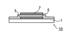
- FIG. 5 is a schematic cross-sectional view showing an exemplary embodiment of a capacitor in one embodiment of the present invention.
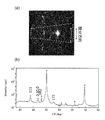
- the two-dimensional X-ray diffraction image of the dielectric film of Example 1 is shown.
- (A) schematically shows the integration direction ( ⁇ direction) when converting the two-dimensional X-ray diffraction image of the dielectric film of Example 1 into an X-ray diffraction pattern (one-dimensional profile), and (b) is.
- the X-ray diffraction pattern (one-dimensional profile) obtained thereby is shown.
- the measurement data of the X-ray diffraction pattern (one-dimensional profile) of the dielectric film of Example 1 and the data which fitted this by the Gaussian function are shown.
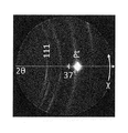
- (A) schematically shows the integration direction (2 ⁇ direction) when the two-dimensional X-ray diffraction image of the dielectric film of Example 1 is converted into a one-dimensional profile with respect to the spot of the orientation plane, and (b) is.
- the measurement data of the one-dimensional profile about the spot of the orientation plane of the dielectric film of Example 1 and the data which fitted this with the Gauss function are shown. It is a graph which evaluated the electrical property of the dielectric film of Example 1.
- a two-dimensional X-ray diffraction image of the dielectric film of Example 2 is shown.
- a two-dimensional X-ray diffraction image of the dielectric film of Comparative Example 1 is shown.
- a two-dimensional X-ray diffraction image of the dielectric film of Comparative Example 2 is shown.
- a two-dimensional X-ray diffraction image of the dielectric film of Comparative Example 3 is shown. It is a graph which evaluated the electrical property at room temperature of the dielectric film in Comparative Examples 1 to 3 and the modified example thereof.
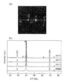
- (A) shows a two-dimensional X-ray diffraction image of the dielectric film of Comparative Example 4, and
- (b) shows an X-ray diffraction pattern (1) of Comparative Example 4 (shown at "900 ° C.") and its modified example. Dimensional profile) is shown. It is a graph which evaluated the electrical property of the dielectric film of the comparative example 4.
- (A) shows a two-dimensional X-ray diffraction image of the dielectric film of Comparative Example 5, and (b) shows an X-ray diffraction pattern (1) of Comparative Example 5 (shown at "900 ° C.") and its modified example. Dimensional profile) is shown. It is a graph which evaluated the electrical property of the dielectric film of the comparative example 5.
- (A) shows a two-dimensional X-ray diffraction image of the dielectric film of Comparative Example 6, and (b) shows an X-ray diffraction pattern (1) of Comparative Example 6 (shown at "900 ° C.”) and its modified example. Dimensional profile) is shown.
- (A) shows a two-dimensional X-ray diffraction image of the dielectric film of Comparative Example 7, and (b) shows an X-ray diffraction pattern (1) of Comparative Example 7 (shown at "900 ° C.") and its modified example. Dimensional profile) is shown.
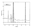
- the X-ray diffraction pattern (one-dimensional profile) of the dielectric film of Comparative Example 8 is shown.
- the X-ray diffraction pattern (one-dimensional profile) of the dielectric film of Comparative Example 9 is shown.
- the dielectric film of this embodiment is It has a pyrochlore-type or layered perovskite-type crystal structure.
- General formula A 2 B 2 O 7 (In the formula, A is Mg, Ca, Sr, Ba, La, Ce, Pr, Nd, Pm, Sm, Eu, Gd, Tb, Dy, Ho, Er, Tm, Yb. Two or more elements selected from the group consisting of and Lu, each containing A 1 and A 2 different from each other, where B is from Ti, Zr, Hf, V, Nb and Ta.
- a 2 B 2 O 7 obtained stoichiometrically by selecting one of each of the elements A and B existing in the dielectric film, the main constituent of the crystal structure of the dielectric film.
- a 1 2 B 1 2 O 7 forming other than the faces (h00), (0k0), (00l), (h0l) and (0kl) (h, k and l are integers excluding 0). It has at least one orientation plane.
- the crystal structure of the oxide having the composition represented by the general formula A 2 B 2 O 7 can usually be a pyrochlore type or a layered perovskite type (also referred to as a perovskite type slab) (these polymorphs can be adopted). Including cases).
- a pyrochlore type or a layered perovskite type also referred to as a perovskite type slab
- the "pyrochlore-type or layered perovskite-type crystal structure” means a crystal structure that may be either one or both of them, and is not construed as being limited to only one of them.
- the dielectric film of the present embodiment has a composition represented by the general formula A 2 B 2 O 7 .
- a and B are symbols that mean (or generically) the elements that occupy the A site and the B site, respectively, in the pyrochlore type or layered perovskite type crystal structure.
- A is two or more selected from the group consisting of Mg, Ca, Sr, Ba, La, Ce, Pr, Nd, Pm, Sm, Eu, Gd, Tb, Dy, Ho, Er, Tm, Yb and Lu.
- A comprises two or more elements selected from the group consisting of Sr, Ba, La and Nd.
- B comprises one or more elements selected from the group consisting of Ti, Zr, Hf, V, Nb and Ta.
- B comprises one or more elements selected from the group consisting of Ti, Nb and Ta.
- a 2 B 2 O 7 is, for example, when A is an element having a trivalent valence and B is an element having a tetravalent valence (that is, A (III) 2 ).
- B (IV) 2 O 7 type) when A is an element having a divalent valence and B is an element having a pentavalent valence (that is, A (II) 2 B (V) 2 O 7 ) Type), and when these are mixed, etc.
- the dielectric film A 1 2 B 1 2 O 7 which is the main component of the crystal structure is identified, and each element of A 1 and B 1 is specifically determined by this. That is, in the dielectric film of the present embodiment, it can be understood that A 1 2 B 1 2 O 7 forms the main body of the crystal structure, and A 2 and other elements that may exist are dissolved therein. ..
- a 1 2 B 1 2 O 7 "forms the main body of the crystal structure" of the dielectric film means that A 1 2 B 1 2 O 7 mainly bears the crystal structure of the dielectric film. means. Which of all the combinations of A 2 B 2 O 7 is "mainly responsible for the crystal structure" A 1 2 B 1 2 O 7 is determined based on the X-ray diffraction pattern obtained from the dielectric film. It is determined to show the crystal structure closest to the crystal structure of the dielectric film.
- a 2 B 2 O 7 is (Sr x La 1-x ) 2 (Ta x Ti 1-x ) 2 O 7 (in the formula, 0 ⁇ x ⁇ 1)
- All combinations obtained stoichiometrically by selecting one each of Sr and La corresponding to B and Ta and Ti corresponding to B are Sr 2 Ta 2 O 7 and La 2 Ti 2 O 7 ( Note that these elements (valences) are Sr (II), La (III), Ta (V), Ti (IV)).
- Known powder X-ray diffraction data can be obtained and used from a database provided by, for example, ICDD (International Center for Diffraction Data).
- a substance other than the dielectric film for example, a substance forming the base of the dielectric film, specifically, a substrate or a conductive member for an electrode if present
- the "alignment plane" of the dielectric film means a plane parallel to the surface of the dielectric film, which is highly oriented, that is, highly crystalline, and more specifically, two-dimensional X-ray diffraction. It is a surface observed in a spot shape in an image, and its surface index (Miller index) is determined with respect to A 1 2 B 1 2 O 7 which is the main component of the crystal structure.
- such alignment surface may have one or more, but with respect to A 1 2 B 1 2 O 7 constituting the main body of the crystal structure of the dielectric film, (h00), In addition to the planes (0k0), (00l), (h0l) and (0kl) (h, k and l are integers excluding 0), it has at least one orientation plane.
- a 1 2 B 1 2 O 7 which forms the main body of the crystal structure is Sr 2 Ta 2 O 7, it is one or more observed in the two-dimensional X-ray diffraction image of the dielectric film.
- the diffraction angle (2 ⁇ ) of a good spot is measured, and on which surface in the powder X-ray diffraction data known for Sr 2 Ta 2 O 7 that the diffraction angle (2 ⁇ ) of the spot is A 1 2 B 1 2 O 7.
- the plane index of one or more oriented planes observed as the spot is determined.
- the plane index of at least one orientation plane thus determined is (h00), (0k0), (00l), (h0l) and (h0l) of Sr 2 Ta 2 O 7 of A 1 2 B 1 2 O 7. Any surface other than the plane (0 kl) (h, k and l are integers excluding 0) may be used.
- the dielectric film of the present embodiment has (h,), (0k0), (00l), (h0l) and (0kl) planes (h,) with respect to A 1 2 B 1 2 O 7 which is the main component of the crystal structure.
- (k and l are integers excluding 0)
- it has at least one orientation plane. This means that the b-axis direction of the crystals forming the dielectric film is not orthogonal to the surface of the dielectric film and is tilted.
- the dielectric film of the present embodiment stably maintains a high relative permittivity over a wide temperature range (for example, 20 to 150 ° C., preferably 20 to 300 ° C.). That is, it can be maintained at a small rate of change.
- a wide temperature range for example, 20 to 150 ° C., preferably 20 to 300 ° C.
- the present invention is not bound by any theory, the reason for which can be considered as follows.
- a dielectric film having a pyrochlore-type or layered perovskite-type crystal structure is provided in the a-axis direction, the b-axis direction, and the c-axis direction in a temperature range of 20 to 150 ° C., more broadly, in a temperature range of 20 to 300 ° C.
- the magnitude of the relative permittivity and the temperature dependence are different.
- the relative permittivity in the a-axis direction and the c-axis direction is higher than the permittivity in the b-axis direction, and a stable slight increase tendency is exhibited.
- the Curie temperature in the a-axis direction and the c-axis direction (the temperature at which the non-dielectric constant rises sharply and shows a peak) is in a high temperature region considerably distant from such a temperature range, while in the b-axis direction.
- Curie temperature is in a low temperature range, not close to such a temperature range.
- the number of elements at the A site is two or more, and A 2 and other elements that may exist are dissolved in A 1 2 B 1 2 O 7 which is the main component of the crystal structure, and the surface of the dielectric film is By tilting the b-axis direction of the crystal, it is considered possible to obtain a higher and stable relative permittivity in the temperature range of 20 to 150 ° C., preferably 20 to 300 ° C.
- the at least one orientation plane of the dielectric film of the present embodiment is (h00), (0k0), (00l), (h0l) as described above with respect to A 1 2 B 1 2 O 7 which is the main body of the crystal structure. ) And (0 kl) planes.
- Such at least one orientation plane is, for example, (111), (131), (151), (115 1), (192), (153), (157), (110), (150), (212). , (172) and (1 130), and the like, but not limited to any one or more.
- h, k and l are all one-digit integers, they are shown according to the notation of (hkl), but when at least one of them is an integer of two or more digits, between integers. Is shown with a space.
- the at least one orientation face of the dielectric film of the present embodiment for A 1 2 B 1 2 O 7 constituting the main body of the crystal structure, other than the above-mentioned surface, and the surface of the (hk0) (h, It is preferable that k and l are planes other than 0). As a result, the b-axis direction of the crystal can be more appropriately tilted with respect to the surface of the dielectric film.
- Such at least one orientation plane is, for example, any one of (111), (131), (151), (115 1), (192), (153), (157), (212) and (172). It may be one or more, but is not limited to this.
- the degree of orientation of at least one of the orientation planes is preferably 0.5 or more and 1 or less, and more preferably 0.8 or more and 1 or less. This makes it possible to orient the dielectric film on this orientation plane at a high rate.
- the "degree of orientation" of a predetermined orientation plane is defined by the Lotgering factor f (-).
- the lotgering factor f is calculated by the following equation (1) using the intensity of X-rays diffracted from a predetermined orientation plane (conveniently referred to as (xyz)).
- f (pp 0 ) / (1-p 0 ) ...
- p 0 is a value based on known powder X-ray diffraction data for A 1 2 B 1 2 O 7 identified as being the main component of the crystal structure
- p is the X-ray of the dielectric film. It is a value based on the diffraction pattern, and is obtained by the following equations (2) and (3), respectively.
- ⁇ I 0 (hkl) is the diffraction intensity of the peaks of all surfaces obtained from the known powder X-ray diffraction data for A 1 2 B 1 2 O 7 (usually, the maximum intensity is 100).
- Relative intensity means the sum of I 0 (xyz) of the diffraction intensity (ibid.) Of the peak of the predetermined orientation plane (xyz) obtained from the known powder X-ray diffraction data for A 1 2 B 1 2 O 7 . Means a value.
- ⁇ I (hkl) means the sum of the diffraction intensities of the peaks of all the surfaces obtained from the X-ray diffraction pattern of the dielectric film
- I (xyz) is the X-ray diffraction pattern of the dielectric film. It means the value of the diffraction intensity of the peak of the predetermined orientation plane (xyz) obtained from.
- the sum of the diffraction intensity areas of all the peaks after fitting is applied as the sum of the diffraction intensities of the peaks of all the surfaces, and the value of the diffraction intensity of the peaks of the predetermined orientation plane (xyz) is a predetermined value after fitting.
- the value of the diffraction intensity area of the peak of the orientation plane (xyz) is applied.
- the variation in the inclination of the crystal axis is preferably 10 ° or less, and more preferably 1 ° or less.
- the dielectric film can be oriented with high crystallinity on this orientation plane.
- the "variation in the inclination of the crystal axis" of the predetermined alignment plane is the half width (°) of the peak of the orientation plane (conveniently referred to as (xyz)) obtained from the X-ray diffraction pattern of the dielectric film. ).
- the portion of the two-dimensional X-ray diffraction image obtained by using the two-dimensional detector that corresponds to the predetermined orientation plane (xyz) is converted into a one-dimensional profile.
- the content ratio of A 1 to the total amount of A can be less than 50 atomic%.
- a 1 is an element that forms the main component of the crystal structure
- the upper limit of its content ratio can be less than 50 atomic%, preferably 40 atomic% or less, more preferably 30 atomic% or less, still more preferably. It was found by the research of the present inventors that it was 20 atomic% or less.
- the lower limit of the content ratio of A 1 can be 5 atomic% or more, preferably 10 atomic% or more in order to form the main body of the crystal structure.
- the content ratio of A 2 to the total amount of A can be 50 atomic% or more.
- a 2 is an element that does not form the main component of the crystal structure and is solid-solved in A 1 2 B 1 2 O 7
- the lower limit of its content ratio can be 50 atomic% or more, which is preferable.
- the upper limit of the content ratio of A 2 can be 95 atomic% or less, preferably 90 atomic% or less so that it can be dissolved in A 1 2 B 1 2 O 7 .
- the content ratio of each element in the dielectric film can be measured by fluorescent X-ray analysis and / or photoelectron spectroscopy.
- the two elements of the A site, A 1 and A 2 preferably have different valences from each other. It is considered that the orientation plane of the dielectric film can be remarkably controlled by the presence of two elements having different valences.
- a 1 may be a divalent element, typically Sr, and A 2 may be a trivalent element, typically La, but is not limited to such combinations.
- the dielectric film of the present embodiment can maintain a high relative permittivity stably, that is, with a small rate of change over a wide temperature range (for example, 20 to 150 ° C., preferably 20 to 300 ° C.).
- the relative permittivity of the dielectric film of the present embodiment ranges from 20 to 150 ° C., preferably 20 to 300 ° C., and the relative permittivity of the bulk single crystal having the same composition (more specifically, the bulk single crystal having the same composition).
- Relative permittivity in the a, b, and c axis directions for example, 70 or more, more preferably 80 or more, particularly preferably 100 or more, and the upper limit is not particularly limited, but for example, 400.
- the rate of change of the relative permittivity of the dielectric film of the present embodiment is preferably 20 to 150 ° C., preferably 20 to 300 ° C., and may be, for example, 10% or less based on the relative permittivity at 20 ° C. Can be less than or equal to 5%.
- the dielectric film of the present embodiment may have an arbitrary appropriate thickness, but may be a thin film.
- the thickness of the dielectric film of the present embodiment can be, for example, 3 nm or more and 1 ⁇ m or less.
- the lower limit is preferably 10 nm or more, and more preferably 50 nm or more from the viewpoint of ensuring insulation (for example, effectively preventing the occurrence of pinholes).
- the upper limit may be 10 ⁇ m or less, but in practice it can be 1 ⁇ m or less, preferably 500 nm or less.
- the dielectric film of the present embodiment may be produced by any suitable method, and can be produced by, for example, the following method.
- the method for producing a dielectric film of the present embodiment is a method for producing a dielectric film having a pyrochlore-type or layered perovskite-type crystal structure.
- A On the surface of the substrate heated to a temperature of 350 to 600 ° C., the general formula A 2 B 2 O 7 (in the formula, A is Mg, Ca, Sr, Ba, La, Ce, Pr, Nd, Pm. , Sm, Eu, Gd, Tb, Dy, Ho, Er, Tm, Yb and Lu, two or more elements selected from the group, each of which is different from each other, A 1 and A 2.
- the precursor film to have is formed by vapor phase deposition, and (b) the substrate on which the precursor film is formed is heat-treated at a temperature of 850 to 1050 ° C. in an atmosphere containing oxygen, and the precursor film is formed.
- the present invention comprises obtaining a dielectric film having a pyrochlore-type or layered perovskite-type crystal structure and having the above composition.
- the temperature at which the substrate is heated in the above step (a) (hereinafter, also simply referred to as “substrate temperature”).
- substrate temperature the temperature at which the substrate on which the precursor was formed is heat-treated in the above step (b)
- PDA temperature (PDA: Post Deposition Annealing) was found to be important (of the dielectric film). Crystallization is considered to proceed not only in step (a) but also in step (b)).
- the substrate is heated at a temperature of 350 to 600 ° C., preferably 400 to 500 ° C. in the above step (a), and a precursor is formed in the above step (b).
- a temperature of 350 to 600 ° C. preferably 400 to 500 ° C. in the above step (a)
- a precursor is formed in the above step (b).
- the material and structure of the substrate are not particularly limited, and can be appropriately selected depending on the use of the dielectric film and the like.
- the substrate may consist of a single material.
- a conductive member which can be used as an electrode, but is not limited to
- a precursor film is formed on the conductive member of the substrate by vapor deposition. Good.
- the surface thereof is preferably the surface (111) or (001). As a result, the relative permittivity of the dielectric film can be maintained high and stable.
- vapor deposition is more specifically physical vapor deposition including sputtering (eg, high frequency (RF) sputtering, pulsed DC sputtering), electron beam deposition, ion plating, and / or metalorganic vapor phase. It can be carried out by applying a growth method (so-called MOCVD, including, for example, atomic layer volumetric method (ALD)), but is not limited thereto.
- a 2 B 2 O 7 is A 1 2 B 1 2 O 7 and A 2 2 B 2 2 O 7 (in the formula, A 1 , A 2 and B 1 are as described above.
- B 2 is, Ti, Zr, Hf, V , a single element of Nb and Ta, are the same or different elements as B 1, comprises a preferably B 1 to be different elements), a 1
- 2 B 1 2 O 7 have a lower crystallization temperature than A 2 2 B 2 2 O 7 .
- a 1 2 B 1 2 O 7 is the main component of the crystal structure. Can be made.
- the "crystallization temperature" of an oxide represented by the general formula A 2 B 2 O 7 and having a predetermined composition is (1) of a conductive substrate made of a crystalline material heated to a certain temperature T. 111)
- a precursor film having the predetermined composition is formed on the surface by vapor phase deposition, and a substrate on which the precursor film is formed is subjected to an oxygen gas flow rate of 0.5 L / min under atmospheric pressure.
- a dielectric film is obtained from the precursor film by heat treatment at a temperature of 900 ° C. for 5 minutes, and the dielectric film is subjected to two-dimensional X-ray diffraction analysis.
- T the lowest temperature T at which at least one spot or ring is observed in the X-ray diffraction image.
- Spots observed in the two-dimensional X-ray diffraction image indicate the presence of a single crystal or a highly oriented crystal structure, and rings observed in the two-dimensional X-ray diffraction image indicate a polycrystalline state. It shows that it has become.
- the dielectric films of La 2 Zr 2 O 7 and Sr 2 Nb 2 O 7 shown in Table 1 were crystallized when the precursor film was formed by vapor phase deposition, they are subjected to heat treatment at 900 ° C. The crystallization temperature was investigated, omitting the above.
- the precursor film may be formed by using one or more raw materials (or may be referred to as a vapor deposition source, a target, etc., the same applies hereinafter).
- the material composition of each raw material may be the same or different from each other.
- a first raw material having a composition of A 1 2 B 1 2 O 7 and a second raw material having a composition of A 2 2 B 2 2 O 7 are used. It may be carried out.
- different vapor phase deposition conditions can be applied to the first and second raw materials.
- the abundance ratio of A 1 and A 2 in the dielectric film, the content ratio of A 1 to the total amount of A, and the content ratio of A 2 to the total amount of A can be controlled.
- an additional raw material having a composition of A 2 B 2 O 7 may or may not be present.
- the vapor phase deposition is carried out under the condition that the growth rate of A 2 2 B 2 2 O 7 from the second raw material is larger than the growth rate of A 1 2 B 1 2 O 7 from the first raw material. be able to.
- the abundance ratio of A 1 / A 2 in the dielectric film can be made small, the content ratio of A 1 to the total amount of A can be made small, and the content ratio of A 2 to the total amount of A can be greatly controlled.
- a from the first raw material is applied by applying a condition in which the output applied to the second raw material is larger than the output applied to the first raw material.
- the growth rate of A 2 2 B 2 2 O 7 from the second raw material can be made larger than the growth rate of 1 2 B 1 2 O 7 .
- the output (power) ratio applied to the first raw material of A 1 2 B 1 2 O 7 and the second raw material of A 2 2 B 2 2 O 7 can be appropriately selected depending on the raw material composition.
- vapor phase deposition of the raw materials from these raw materials on the surface of the substrate can be carried out in any appropriate manner.
- the raw materials may be simultaneously vapor-phase-deposited on the surface of the substrate from these raw materials to form the precursor film in the form of a simultaneous mixed film.
- the raw materials are applied to the surface of the substrate from these raw materials non-simultaneously (the vapor phase deposition period from each raw material may or may not partially overlap, and is repeated regularly or irregularly.
- the precursor may be formed in the form of a fusion film in which these raw materials are fused with each other by vapor-phase deposition (for example, laminating). Fusion can occur spontaneously without the addition of further external energy, as crystal growth and element diffusion are brought about by the thermal energy transferred from the substrate and the kinetic energy applied to the raw material during vapor phase deposition.
- step (b) of the method for producing a dielectric film of the present embodiment it is considered that crystallization further progresses in the film by heat-treating the precursor film (crystallization in step (b) It is understood as "additional crystallization").
- the heat treatment is preferably carried out in a gas atmosphere containing oxygen.
- the gas containing oxygen is not particularly limited, and air may be conveniently used under atmospheric pressure, or oxygen gas substantially composed of oxygen (for example, an oxygen concentration of 99% or more) may be used. ..
- the gas containing oxygen does not have to be flowed during the heat treatment, but it is more preferable to flow it, and in the latter case, the flow rate can be 0.1 to 1 L / min.
- the heat treatment time can be appropriately selected, and can be, for example, 2 minutes or more and 60 minutes or less.
- the dielectric film of the present embodiment is not limited to that obtained by such a manufacturing method, and can be obtained by any other suitable manufacturing method. It may be a product.
- a sol-gel method may be used instead of the vapor phase deposition method.
- the capacitor of the present embodiment includes an electrode and a dielectric film described in detail in the first embodiment arranged on the electrode.
- Such a capacitor can be a so-called thin film capacitor.
- the capacitor of the present embodiment may have any suitable configuration as long as it includes an electrode and a dielectric film arranged on the electrode, and is not particularly limited.
- the capacitor 10 may be configured by sandwiching the dielectric film 5 between the two electrodes 3 and 7 (in the embodiment (parallel plate type) shown in FIG. 1, the electrodes 3 and 7 are , Can be individually connected to leader wires at appropriate locations in the depth direction (not shown).
- a capacitor may be formed by providing a dielectric film straddling two electrodes existing apart from each other.
- the capacitor manufacturing method of the present embodiment may be manufactured by any suitable method, but can be typically carried out including the dielectric film manufacturing method described in detail in the first embodiment.
- the lower electrode 3, the dielectric film 5, and the upper electrode 7 may be sequentially laminated and formed on the surface of the substrate 1 to manufacture the capacitor 10.
- two electrodes may be formed on the surface of the substrate so as to be separated from each other, and a dielectric film may be formed so as to straddle them to manufacture a capacitor.
- the method for forming the dielectric film corresponds to the manufacturing method detailed in the first embodiment, and the method for forming the electrode may be any known suitable method.
- the conductive materials constituting the electrodes are, for example, Pt, Ti, W, Al, Ni, Ag, Au, Pd, Ir, Rh, TiC, TaC, TiN, Ag 2 O, Ru, Ru 2 O, SrRuO 3 , Nb. It may be added SrTiO 3, or the like, and may be, for example, one layer or a laminate of two or more layers.
- the material constituting the substrate is not particularly limited, for example Si, or and the like oxide single crystals such as SrTiO 3. Any suitable material layer, such as the SiO 2 layer, may be present between the substrate and the electrodes.
- the capacitor of the present embodiment has the same effect as the dielectric film described in detail in the first embodiment.
- the surface of the electrode in contact with the dielectric film is preferably the surface of (111) or (001), for example. More specifically, when the electrode is made of a crystalline material, the preferred orientation exhibited by the surface of the electrode may differ depending on the crystal structure of the crystalline material. For example, at least according crystallinity material, cubic material (e.g. Pt, W, Al, Ni, Ag, Au, Pd, Ir, Rh, TiC, TaC, is selected from the group consisting of TiN and Ag 2 O, etc. If it is one), if a tetragonal materials (e.g. Ru 2 O, etc.), or is a perovskite oxide (cubic) (e.g.
- Example 1 This embodiment relates to a dielectric film having a composition represented by (Sr x La 1-x ) 2 (Ta x Ti 1-x ) 2 O 7 and a capacitor including such a dielectric film.
- a Si (100) substrate having a SiO 2 film with a thickness of about 300 nm on its surface is prepared, and a Ti layer with a thickness of about 10 nm and a thickness of about 100 nm are formed on the surface by DC sputtering.
- the Pt layers were sequentially laminated to form a lower electrode composed of these layers.
- the temperature of the substrate was set to room temperature (about 20 ° C.).
- the Ti layer was provided as a relatively thin layer in order to improve the adhesion between the SiO 2 film and the Pt layer.
- the Pt layer is the main body portion of the lower electrode, whereby the electrode surface of the (111) plane is formed.
- the substrate on which the lower electrode is formed as described above is heated to 400 ° C. (that is, the substrate temperature is 400 ° C.), and then RF sputtering is performed on the substrate (Sr x La 1-).
- x ) 2 (Ta x Ti 1-x ) A precursor film having a composition represented by 2 O 7 was formed (note that a part (end) of the lower electrode did not form a precursor on it. I left it exposed).
- RF sputtering uses the target of the Sr 2 Ta 2 O 7 raw material and the target of the La 2 Ti 2 O 7 raw material as the vapor deposition source, and determines the RF power ratio of the Sr 2 Ta 2 O 7 raw material: La 2 Ti 2 O 7 raw material. It was vapor-deposited at the same time as 20W: 60W. The oxygen concentration in the ambient atmosphere of the substrate was 5%.
- the substrate on which the precursor film was formed as described above is subjected to heat treatment at 900 ° C. for 5 minutes while oxygen gas is allowed to flow at 0.5 L / min. (I.e., PDA temperature 900 ° C.), a dielectric film having a composition represented by (Sr x La 1-x ) 2 (Ta x Ti 1-x ) 2 O 7 is formed from the precursor film. did.
- the thickness of the obtained dielectric film was about 200 nm.
- a Pt layer having a thickness of about 150 nm was formed as an upper electrode in a substantially circular shape having a diameter of about 110 nm by DC sputtering.
- the temperature of the substrate was set to room temperature (about 20 ° C.).
- room temperature about 20 ° C.
- FIG. 3A the results are shown in FIG. 3 (b).
- the symbol “*” indicates a peak caused by a substance other than the dielectric film (Pt, Ti, SiO 2 and Si) and is ignored because it does not constitute the dielectric film (described later).
- FIGS. 13 (b), 15 (b), 17 (b), 19 (b), 21, and 22), and the peak near 2 ⁇ 40 ° is due to Pt).
- the dielectric film of this example was compared with the known powder X-ray diffraction data (ICDD) of Sr 2 Ta 2 O 7 and La 2 Ti 2 O 7 (the following examples and comparative examples).
- ICDD powder X-ray diffraction data
- the known data used in the above are appropriately selected depending on the raw materials used as the deposition source), and it was identified that Sr 2 Ta 2 O 7 is the main component of the crystal structure.
- Orientation degree of orientation plane Each peak (however, peaks caused by substances other than the dielectric film are excluded) was fitted by a Gaussian function from the X-ray diffraction pattern (one-dimensional profile) of the dielectric film obtained above. The results are shown in FIG. 4 (in the figure, the measurement data of the one-dimensional profile is shown by a solid line, and the data fitted by the Gaussian function is shown by a dotted line). From this fitting, p was calculated by calculating the ratio of the diffraction intensity area of the peak of the orientation plane (111) to the sum of the diffraction intensity areas of all the peaks.
- the arc region including the spot of the orientation plane (111) of the two-dimensional X-ray diffraction image is set in the 2 ⁇ direction, in the dotted line region schematically shown in FIG. 5 (a).
- the integration was performed to obtain a one-dimensional profile, and the peak of the orientation plane (111) was fitted by a Gaussian function.
- FIG. 5 (b) in the figure, the measurement data of the one-dimensional profile is shown by a solid line, and the data (including the background) fitted by the Gaussian function is shown by a dotted line). From this fitting, the half width (°) of the peak of the orientation plane (111) was measured and found to be 6.42 °.
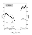
- the electrical characteristics of the dielectric film of this example were evaluated. More specifically, a DC voltage of 3 V is applied between the upper electrode and the lower electrode of the capacitor manufactured as described above, and the relative permittivity (-), the dielectric loss (-) and the dielectric loss (-) are applied at a measurement frequency of 1 MHz. The current density (A / cm 2 ) was measured. The results are shown in FIG. As can be understood from FIG. 6, the dielectric film of this embodiment exhibits a high relative permittivity exceeding 100 over 20 to 300 ° C., and the rate of change thereof is based on the relative permittivity at 20 ° C. It was less than 5%. Further, the dielectric film of this example showed a double-digit increase rate of the current density over 20 to 300 ° C., but showed a dielectric loss of less than 0.1 and functioned as a dielectric.
- Example 2 The present embodiment relates to a dielectric film having a composition represented by (Sr x La 1-x ) 2 (Nb x Ti 1-x ) 2 O 7 and a capacitor having such a dielectric film. Unless otherwise specified, the same description as in Example 1 applies (the same applies to the examples and comparative examples described in the present specification).
- step (a) the substrate was heated to 500 ° C. (that is, the substrate temperature was 500 ° C.), and RF sputtering used the target of the Sr 2 Nb 2 O 7 raw material and the La 2 Ti 2 O 7 raw material as the vapor deposition source.
- the RF power ratio of the Sr 2 Nb 2 O 7 raw material: La 2 Ti 2 O 7 raw material was set to 50 W: 60 W, and the film was simultaneously vapor-deposited to (Sr x La 1-x ) 2 (Nb x Ti 1-).
- Example 2 Example 2
- a dielectric film having a composition represented by (1) was formed to obtain a capacitor (the PDA temperature was set to 900 ° C. as in Example 1). The thickness of the obtained dielectric film was about 200 nm.
- FIG. 7 Main body and orientation plane of crystal structure A two-dimensional X-ray diffraction image of this dielectric film is shown in FIG.
- Sr 2 Nb 2 O 7 mainly forms the crystal structure of the X-ray diffraction pattern.
- orientation degree of orientation plane The orientation degree of the orientation plane (150) of this dielectric film was 0.68.
- Figure 8 shows the results of evaluation of the electrical characteristics of the dielectric film of this example.
- the dielectric film of this embodiment exhibits a high relative permittivity exceeding 100 over 20 to 150 ° C., and the rate of change thereof is based on the relative permittivity at 20 ° C. It was less than 5%.
- the dielectric film of this example showed high insulating properties having a current density of 1 ⁇ 10 -7 A / cm 2 or less and a dielectric loss of 0.05 or less.
- the dielectric film of this example had a large leakage current at a temperature exceeding 160 ° C., and its electrical characteristics were not evaluated.
- This comparative example relates to a dielectric film having a composition represented by (Sr x La 1-x ) 2 (Ta x Ti 1-x ) 2 O 7 and a capacitor having such a dielectric film.
- Tables show the heating temperature of the substrate in step (a), the RF power ratio of the Sr 2 Ta 2 O 7 raw material: La 2 Ti 2 O 7 raw material, and the heat treatment temperature (PDA temperature) in step (b).
- a dielectric film having a composition represented by (Sr x La 1-x ) 2 (Ta x Ti 1-x ) 2 O 7 in the same manner as in Example 1 except that they are different as shown in 2. was formed to obtain a capacitor. The thickness of the obtained dielectric film is also shown in Table 2.
- FIGS. 9 to 11 Two-dimensional X-ray diffraction images of the dielectric films of Comparative Examples 1 to 3 are shown in FIGS. 9 to 11, respectively.
- Sr 2 Ta 2 O 7 mainly forms the crystal structure.
- Orientation degree of orientation plane The orientation degree of the orientation plane (041) of the dielectric film of Comparative Example 1 was 0.66. Although the dielectric film of Comparative Example 2 was not an orientation plane, the degree of orientation of (080) was 0.065, and the degree of orientation of (010) was 0.22. The dielectric film of Comparative Example 3 was not an alignment plane, but the degree of orientation of (111) was 0.30.
- the dielectric film of Comparative Example 1 exhibited a relative permittivity of about 45 and a dielectric loss of about 0.05 at room temperature (about 20 ° C.).
- the dielectric film of Comparative Example 2 exhibited a relative permittivity of about 30 and a dielectric loss of about 0.05 at room temperature (about 20 ° C.).
- the dielectric film of Comparative Example 3 exhibited a relative permittivity of about 600 and a dielectric loss of about 0.05 at room temperature (about 20 ° C.).
- Comparative Examples 1 to 3 were modified (each distance from the two vapor deposition sources was made different, etc.), and (Sr x La 1-x ) 2 (Ta x Ti 1-x ) 2 O 7 .
- the dielectric films and capacitors having different x in the formula were obtained, and the results of evaluating the electrical characteristics at room temperature (about 20 ° C.) are shown in FIG. 12 (in FIG. 12). indicating "xSr 2 Ta 2 O 7 - ( 1-x) La 2 Ti 2 O 7 " is a representation of the raw material base, (Sr x La 1-x ) 2 (Ta x Ti 1-x) 2 O 7 as synonymous). In each case, the relative permittivity was as low as less than 70.
- This comparative example relates to a dielectric film having a composition represented by Sr 2 Ta 2 O 7 and a capacitor including such a dielectric film.
- the substrate temperature was 500 ° C. and the PDA temperature was 900 ° C.
- the thickness of the obtained dielectric film was about 200 nm.
- the dielectric film of this comparative example has a composition of Sr 2 Ta 2 O 7 , and the element of A is only Sr.
- Sr 2 Ta 2 O 7 is the main component of the crystal structure.
- step (b) It is an X-ray diffraction pattern of the film after forming and before subjecting to step (b), and "700 ° C.” and “800 ° C.” set the heat treatment (PDA temperature) in step (b) to 700 ° C. It is an X-ray diffraction pattern of the obtained dielectric film. From FIG. 13B, it can be understood that a PDA temperature of 900 ° C. is required to bring about the orientation planes (110) and (200) by crystallization in this dielectric film.
- Orientation degree of alignment plane The orientation degree of the orientation plane (110) of the dielectric film of this comparative example was 0.81, and the orientation degree of the orientation plane (200) was 0.08.
- FIG. 14 shows the results of evaluation of the electrical characteristics of the dielectric film of this comparative example. As can be seen from FIG. 14, the dielectric film of this comparative example exhibited a low relative permittivity of about 45 to 55 over 20 to 300 ° C.
- This comparative example relates to a dielectric film having a composition represented by Sr 2 Nb 2 O 7 and a capacitor including such a dielectric film.
- a dielectric film having a composition represented by Sr 2 Nb 2 O 7 was formed in the same manner as in Example 1 except that a precursor film having a composition represented by 7 was formed to obtain a capacitor. (Similar to Example 1, the substrate temperature was 500 ° C. and the PDA temperature was 900 ° C.). The thickness of the obtained dielectric film was about 200 nm.
- the dielectric film of this comparative example has a composition of Sr 2 Nb 2 O 7 , and the element A is only Sr.
- Sr 2 Nb 2 O 7 is the main component of the crystal structure.
- the dielectric film of this comparative example has no orientation plane (in other words, the (131) plane and (in other words, the (131) plane) and ( 150) The plane is not an oriented plane).
- the X-ray diffraction pattern of the film obtained by modifying this comparative example is also shown in FIG. 15 (b), and “after film formation” indicates the precursor film of step (a). It is an X-ray diffraction pattern of the film after forming and before subjecting to step (b), and "700 ° C.” and "800 ° C.” set the heat treatment (PDA temperature) in step (b) to 700 ° C. and 800 ° C., respectively. It is an X-ray diffraction pattern of the obtained dielectric film.
- orientation degree of orientation plane Although the dielectric film of this comparative example is not an orientation plane, the orientation degree of (131) was 0.52 and the orientation degree of (150) was 0.30.
- Figure 16 shows the results of evaluation of the electrical characteristics of the dielectric film of this comparative example. As can be understood from FIG. 16, the dielectric film of this comparative example exhibited a low relative permittivity of about 40 to 60 over 20 to 300 ° C.
- This comparative example relates to a dielectric film having a composition represented by La 2 Ti 2 O 7 and a capacitor including such a dielectric film.
- the RF sputtering, using La 2 Ti 2 O 7 raw material target as evaporation source, and the La 2 Ti 2 O 7 raw RF power deposited as 50W, La 2 Ti 2 O A capacitor was obtained by forming a dielectric film having a composition represented by La 2 Ti 2 O 7 in the same manner as in Example 1 except that a precursor film having a composition represented by 7 was formed.
- the substrate temperature was 500 ° C. and the PDA temperature was 900 ° C.
- the thickness of the obtained dielectric film was about 80 nm.
- the dielectric film of this comparative example has a composition of La 2 Ti 2 O 7 , and the element A is only La.
- La 2 Ti 2 O 7 mainly forms the crystal structure.
- the dielectric film of this comparative example does not have an orientation plane (in other words, the (400) plane is orientation. Not a face).
- the X-ray diffraction pattern of the film obtained by modifying this comparative example is also shown in FIG. 17 (b), and “after film formation” indicates the precursor film of step (a). It is an X-ray diffraction pattern of the film after forming and before subjecting to step (b), and "700 ° C.” and "800 ° C.” set the heat treatment (PDA temperature) in step (b) to 700 ° C. It is an X-ray diffraction pattern of the obtained dielectric film.
- orientation degree of orientation plane Although the dielectric film of this comparative example is not an orientation plane, the orientation degree of (400) was 0.534.
- This comparative example relates to a dielectric film having a composition represented by La 2 Zr 2 O 7 and a capacitor including such a dielectric film.
- the RF sputtering, using a La 2 Zr 2 O 7 raw material target as evaporation source, and the La 2 Zr 2 O 7 raw RF power deposited as 50W, La 2 Zr 2 O A capacitor was obtained by forming a dielectric film having a composition represented by La 2 Zr 2 O 7 in the same manner as in Example 1 except that a precursor film having a composition represented by 7 was formed.
- the substrate temperature was 500 ° C. and the PDA temperature was 900 ° C.
- the thickness of the obtained dielectric film was about 60 nm.
- the dielectric film of this comparative example has a composition of La 2 Zr 2 O 7 , and the element A is only La.
- La 2 Zr 2 O 7 mainly forms the crystal structure.
- the dielectric film of this comparative example was ( It was found to have an orientation plane of 222) (in other words, the (444) plane is not an orientation plane).
- the X-ray diffraction pattern of the film obtained by modifying this comparative example is also shown in FIG. 18 (b), and “after film formation” indicates the precursor film of step (a). It is an X-ray diffraction pattern of the film after forming and before subjecting to step (b), and "700 ° C.” and "800 ° C.” set the heat treatment (PDA temperature) in step (b) to 700 ° C. It is an X-ray diffraction pattern of the obtained dielectric film.
- Orientation degree of orientation plane In the dielectric film of this comparative example, the orientation degree of the orientation plane (222) was 0.97.
- This comparative example relates to a dielectric film having a composition represented by Sr 2 (Ta x Nb 1-x ) 2 O 7 and a capacitor including such a dielectric film.
- RF sputtering uses a target of Sr 2 Ta 2 O 7 raw material and a target of Sr 2 Nb 2 O 7 raw material as a vapor deposition source, and Sr 2 Ta 2 O 7 raw material: Sr 2 Nb.
- the RF power ratio of the 2 O 7 raw material is 50 W: 50 W
- the opening area is alternately vapor-deposited via a controllable shutter mechanism to obtain a composition represented by Sr 2 (Ta x Nb 1-x ) 2 O 7.
- a capacitor was obtained by forming a dielectric film having a composition represented by Sr 2 (Ta x Nb 1-x ) 2 O 7 in the same manner as in Example 1 except that the precursor film having the precursor film was formed. (Similar to Example 1, the substrate temperature was 500 ° C. and the PDA temperature was 900 ° C.). The thickness of the obtained dielectric film was about 70 nm.
- the composition can be inclined in the dielectric film, which is generally close to the Sr 2 Ta 2 O 7 raw material. The region became Sr 2 Ta 2 O 7 rich, and the region close to the Sr 2 Nb 2 O 7 raw material became Sr 2 Nb 2 O 7 rich.
- xSr 2 Ta 2 O 7 - ( 1-x) Sr 2 Nb 2 O 7 is a representation of the raw material base, synonymous with Sr 2 (Ta x Nb 1- x) 2 O 7 Is).
- the relative permittivity at room temperature (25 ° C.) is 60 or less, which is a high relative permittivity. Was not obtained.
- This comparative example relates to a dielectric film having a composition represented by La 2 (Zr x Ti 1-x ) 2 O 7 and a capacitor including such a dielectric film.
- step (a) the substrate was heated to 550 ° C (that is, the substrate temperature was 550 ° C), and RF sputtering was performed as a vapor deposition source for the target of the La 2 Zr 2 O 7 raw material and the La 2 Ti 2 O 7 raw material.
- RF sputtering was performed as a vapor deposition source for the target of the La 2 Zr 2 O 7 raw material and the La 2 Ti 2 O 7 raw material.
- La 2 Zr 2 O 7 raw material La 2 Ti 2 O 7 raw RF power ratio of the 50 W: as 50 W
- by depositing alternately via a controllable shutter mechanism opening area La 2 ( Zr x Ti 1-x ) La 2 (Zr x Ti 1-x ) 2 O 7 in the same manner as in Example 1 except that a precursor film having a composition represented by 2 O 7 was formed.
- a dielectric film having the composition to be obtained was formed to obtain a capacitor (the PDA temperature was set to 900 ° C. as in Example 1). The
- the composition gradient can be generated in the dielectric film, and is generally close to the La 2 Zr 2 O 7 raw material. The region became La 2 Zr 2 O 7 rich, and the region close to the La 2 Ti 2 O 7 raw material became La 2 Ti 2 O 7 rich.
- xLa 2 Zr 2 O 7 - ( 1-x) La 2 Ti 2 O 7 is a representation of the raw material base, La 2 (Zr x Ti 1 -x) 2 O 7 as defined Is).
- x 1.0, the dielectric film of Comparative Example 7 had an orientation plane (222).
- Comparative Examples 6 and 7 have a substrate temperature of 500 ° C., unlike this Comparative Example.
- X 0, 0.2, 0.4, 0.6, 0.8 and 1
- the relative permittivity at room temperature (25 ° C.) was 50 or less, and a high relative permittivity could not be obtained.
- the leakage current exceeded 1 mA at 50 ° C. or higher, and the electrical characteristics could not be evaluated.
- the dielectric film of the present invention is suitably used as a dielectric film in a capacitor (particularly a thin film capacitor), and such a capacitor can be used for various electronic components, but the dielectric film of the present invention is not limited to such applications. ..
Landscapes
- Chemical & Material Sciences (AREA)
- Organic Chemistry (AREA)
- Materials Engineering (AREA)
- Engineering & Computer Science (AREA)
- Mechanical Engineering (AREA)
- Metallurgy (AREA)
- Chemical Kinetics & Catalysis (AREA)
- Inorganic Chemistry (AREA)
- General Chemical & Material Sciences (AREA)
- Inorganic Compounds Of Heavy Metals (AREA)
- Physical Vapour Deposition (AREA)
- Chemical Vapour Deposition (AREA)
- Inorganic Insulating Materials (AREA)
- Formation Of Insulating Films (AREA)
- Semiconductor Memories (AREA)
Priority Applications (1)
| Application Number | Priority Date | Filing Date | Title |
|---|---|---|---|
| JP2021524802A JP7226747B2 (ja) | 2019-06-05 | 2020-05-28 | 誘電体膜およびそれを用いたキャパシタならびに誘電体膜の製造方法 |
Applications Claiming Priority (2)
| Application Number | Priority Date | Filing Date | Title |
|---|---|---|---|
| JP2019-105680 | 2019-06-05 | ||
| JP2019105680 | 2019-06-05 |
Publications (1)
| Publication Number | Publication Date |
|---|---|
| WO2020246363A1 true WO2020246363A1 (ja) | 2020-12-10 |
Family
ID=73652521
Family Applications (1)
| Application Number | Title | Priority Date | Filing Date |
|---|---|---|---|
| PCT/JP2020/021128 Ceased WO2020246363A1 (ja) | 2019-06-05 | 2020-05-28 | 誘電体膜およびそれを用いたキャパシタならびに誘電体膜の製造方法 |
Country Status (2)
| Country | Link |
|---|---|
| JP (1) | JP7226747B2 (https=) |
| WO (1) | WO2020246363A1 (https=) |
Cited By (2)
| Publication number | Priority date | Publication date | Assignee | Title |
|---|---|---|---|---|
| CN120136549A (zh) * | 2025-05-16 | 2025-06-13 | 苏州工学院 | 一种低损耗稀土烧绿石基微波介质陶瓷材料及其制备方法 |
| WO2026023204A1 (ja) * | 2024-07-26 | 2026-01-29 | Jx金属株式会社 | 酸化物スパッタリングターゲット及びその製造方法並びに酸化物粉末 |
Citations (5)
| Publication number | Priority date | Publication date | Assignee | Title |
|---|---|---|---|---|
| JP2003502837A (ja) * | 1999-06-10 | 2003-01-21 | シメトリックス・コーポレーション | 高誘電率用途向け金属酸化物薄膜 |
| JP2003209179A (ja) * | 2002-01-15 | 2003-07-25 | Fujitsu Ltd | 容量素子及びその製造方法 |
| JP2005216951A (ja) * | 2004-01-27 | 2005-08-11 | Matsushita Electric Ind Co Ltd | 層状反強誘電体、キャパシタとメモリ及びそれらの製造方法 |
| CN101752410A (zh) * | 2008-12-15 | 2010-06-23 | 北京有色金属研究总院 | 一种用于高介电常数栅介质的外延薄膜及其制备方法 |
| JP2011210783A (ja) * | 2010-03-29 | 2011-10-20 | Kyocera Corp | 積層セラミックコンデンサ |
-
2020
- 2020-05-28 JP JP2021524802A patent/JP7226747B2/ja active Active
- 2020-05-28 WO PCT/JP2020/021128 patent/WO2020246363A1/ja not_active Ceased
Patent Citations (5)
| Publication number | Priority date | Publication date | Assignee | Title |
|---|---|---|---|---|
| JP2003502837A (ja) * | 1999-06-10 | 2003-01-21 | シメトリックス・コーポレーション | 高誘電率用途向け金属酸化物薄膜 |
| JP2003209179A (ja) * | 2002-01-15 | 2003-07-25 | Fujitsu Ltd | 容量素子及びその製造方法 |
| JP2005216951A (ja) * | 2004-01-27 | 2005-08-11 | Matsushita Electric Ind Co Ltd | 層状反強誘電体、キャパシタとメモリ及びそれらの製造方法 |
| CN101752410A (zh) * | 2008-12-15 | 2010-06-23 | 北京有色金属研究总院 | 一种用于高介电常数栅介质的外延薄膜及其制备方法 |
| JP2011210783A (ja) * | 2010-03-29 | 2011-10-20 | Kyocera Corp | 積層セラミックコンデンサ |
Cited By (2)
| Publication number | Priority date | Publication date | Assignee | Title |
|---|---|---|---|---|
| WO2026023204A1 (ja) * | 2024-07-26 | 2026-01-29 | Jx金属株式会社 | 酸化物スパッタリングターゲット及びその製造方法並びに酸化物粉末 |
| CN120136549A (zh) * | 2025-05-16 | 2025-06-13 | 苏州工学院 | 一种低损耗稀土烧绿石基微波介质陶瓷材料及其制备方法 |
Also Published As
| Publication number | Publication date |
|---|---|
| JP7226747B2 (ja) | 2023-02-21 |
| JPWO2020246363A1 (https=) | 2020-12-10 |
Similar Documents
| Publication | Publication Date | Title |
|---|---|---|
| CN102858691B (zh) | 具有阴离子控制的介电性质的钙钛矿材料、薄膜电容器器件及其制造方法 | |
| US7095067B2 (en) | Oxidation-resistant conducting perovskites | |
| JPWO2016031986A1 (ja) | 強誘電性薄膜、電子素子及び製造方法 | |
| Jie et al. | Enhanced dielectric characteristics of preferential (1 1 1)-oriented BZT thin films by manganese doping | |
| JPWO2005102958A1 (ja) | 薄膜容量素子用組成物、高誘電率絶縁膜、薄膜容量素子、薄膜積層コンデンサおよび薄膜容量素子の製造方法 | |
| JP7226747B2 (ja) | 誘電体膜およびそれを用いたキャパシタならびに誘電体膜の製造方法 | |
| US10475586B2 (en) | Oxynitride thin film and capacitance element | |
| US10115887B2 (en) | Ferroelectric ceramics and method for manufacturing the same | |
| Mahesh et al. | Improved tunability and energy storage density properties of low-loss, lead-free (Ba0. 50Sr0. 50) TiO3 and Ba (Zr0. 15Ti0. 85) O3 bilayer thin film stacks | |
| JP6981280B2 (ja) | 多結晶誘電体薄膜および容量素子 | |
| US6824898B2 (en) | Dielectric thin film, method for making the same and electric components thereof | |
| US20060237760A1 (en) | Thin-film capacitative element and electronic circuit and electronic equipment including the same | |
| WO2004112056A1 (ja) | 積層体ユニット | |
| TWI672283B (zh) | 氮氧化物薄膜與電容元件 | |
| JP7000883B2 (ja) | 酸窒化物薄膜および容量素子 | |
| KR101013762B1 (ko) | 전계 가변형 BST-Pb계 파이로클로어 복합 유전체박막과 제조방법 | |
| EP3382726A1 (en) | Oxynitride thin film and capacitance element | |
| Wu et al. | Preparation and conductive properties of neodymium-doped lanthanum nickelate thin films by chemical solution deposition method | |
| JP2022182764A (ja) | 誘電体膜およびそれを用いたキャパシタならびに誘電体膜の製造方法 | |
| Huang et al. | Film thickness dependence of the dielectric properties of SrTiO3/BaTiO3 multilayer thin films deposited by double target RF magnetron sputtering | |
| KR100591931B1 (ko) | 전계 가변형 Pb계 파이로클로어 유전체 박막과 제조 방법 | |
| CN109767915B (zh) | 金属氮氧化物薄膜及金属氮氧化物薄膜的制造方法、以及电容元件 | |
| US20040164416A1 (en) | Multi-layered unit | |
| US20060186395A1 (en) | Thin-film capacitative element and electronic circuit and electronic equipment including the same | |
| KR100219834B1 (ko) | 우선 배향성 강유전 박막의 제조방법 |
Legal Events
| Date | Code | Title | Description |
|---|---|---|---|
| 121 | Ep: the epo has been informed by wipo that ep was designated in this application |
Ref document number: 20817618 Country of ref document: EP Kind code of ref document: A1 |
|
| ENP | Entry into the national phase |
Ref document number: 2021524802 Country of ref document: JP Kind code of ref document: A |
|
| NENP | Non-entry into the national phase |
Ref country code: DE |
|
| 122 | Ep: pct application non-entry in european phase |
Ref document number: 20817618 Country of ref document: EP Kind code of ref document: A1 |