WO2020246363A1 - Dielectric film, capacitor using same, and dielectric film production method - Google Patents
Dielectric film, capacitor using same, and dielectric film production method Download PDFInfo
- Publication number
- WO2020246363A1 WO2020246363A1 PCT/JP2020/021128 JP2020021128W WO2020246363A1 WO 2020246363 A1 WO2020246363 A1 WO 2020246363A1 JP 2020021128 W JP2020021128 W JP 2020021128W WO 2020246363 A1 WO2020246363 A1 WO 2020246363A1
- Authority
- WO
- WIPO (PCT)
- Prior art keywords
- dielectric film
- ray diffraction
- raw material
- comparative example
- plane
- Prior art date
Links
Images


Classifications
-
- C—CHEMISTRY; METALLURGY
- C01—INORGANIC CHEMISTRY
- C01G—COMPOUNDS CONTAINING METALS NOT COVERED BY SUBCLASSES C01D OR C01F
- C01G35/00—Compounds of tantalum
-
- C—CHEMISTRY; METALLURGY
- C23—COATING METALLIC MATERIAL; COATING MATERIAL WITH METALLIC MATERIAL; CHEMICAL SURFACE TREATMENT; DIFFUSION TREATMENT OF METALLIC MATERIAL; COATING BY VACUUM EVAPORATION, BY SPUTTERING, BY ION IMPLANTATION OR BY CHEMICAL VAPOUR DEPOSITION, IN GENERAL; INHIBITING CORROSION OF METALLIC MATERIAL OR INCRUSTATION IN GENERAL
- C23C—COATING METALLIC MATERIAL; COATING MATERIAL WITH METALLIC MATERIAL; SURFACE TREATMENT OF METALLIC MATERIAL BY DIFFUSION INTO THE SURFACE, BY CHEMICAL CONVERSION OR SUBSTITUTION; COATING BY VACUUM EVAPORATION, BY SPUTTERING, BY ION IMPLANTATION OR BY CHEMICAL VAPOUR DEPOSITION, IN GENERAL
- C23C14/00—Coating by vacuum evaporation, by sputtering or by ion implantation of the coating forming material
- C23C14/06—Coating by vacuum evaporation, by sputtering or by ion implantation of the coating forming material characterised by the coating material
- C23C14/08—Oxides
-
- C—CHEMISTRY; METALLURGY
- C23—COATING METALLIC MATERIAL; COATING MATERIAL WITH METALLIC MATERIAL; CHEMICAL SURFACE TREATMENT; DIFFUSION TREATMENT OF METALLIC MATERIAL; COATING BY VACUUM EVAPORATION, BY SPUTTERING, BY ION IMPLANTATION OR BY CHEMICAL VAPOUR DEPOSITION, IN GENERAL; INHIBITING CORROSION OF METALLIC MATERIAL OR INCRUSTATION IN GENERAL
- C23C—COATING METALLIC MATERIAL; COATING MATERIAL WITH METALLIC MATERIAL; SURFACE TREATMENT OF METALLIC MATERIAL BY DIFFUSION INTO THE SURFACE, BY CHEMICAL CONVERSION OR SUBSTITUTION; COATING BY VACUUM EVAPORATION, BY SPUTTERING, BY ION IMPLANTATION OR BY CHEMICAL VAPOUR DEPOSITION, IN GENERAL
- C23C14/00—Coating by vacuum evaporation, by sputtering or by ion implantation of the coating forming material
- C23C14/22—Coating by vacuum evaporation, by sputtering or by ion implantation of the coating forming material characterised by the process of coating
- C23C14/34—Sputtering
-
- C—CHEMISTRY; METALLURGY
- C23—COATING METALLIC MATERIAL; COATING MATERIAL WITH METALLIC MATERIAL; CHEMICAL SURFACE TREATMENT; DIFFUSION TREATMENT OF METALLIC MATERIAL; COATING BY VACUUM EVAPORATION, BY SPUTTERING, BY ION IMPLANTATION OR BY CHEMICAL VAPOUR DEPOSITION, IN GENERAL; INHIBITING CORROSION OF METALLIC MATERIAL OR INCRUSTATION IN GENERAL
- C23C—COATING METALLIC MATERIAL; COATING MATERIAL WITH METALLIC MATERIAL; SURFACE TREATMENT OF METALLIC MATERIAL BY DIFFUSION INTO THE SURFACE, BY CHEMICAL CONVERSION OR SUBSTITUTION; COATING BY VACUUM EVAPORATION, BY SPUTTERING, BY ION IMPLANTATION OR BY CHEMICAL VAPOUR DEPOSITION, IN GENERAL
- C23C14/00—Coating by vacuum evaporation, by sputtering or by ion implantation of the coating forming material
- C23C14/58—After-treatment
-
- C—CHEMISTRY; METALLURGY
- C23—COATING METALLIC MATERIAL; COATING MATERIAL WITH METALLIC MATERIAL; CHEMICAL SURFACE TREATMENT; DIFFUSION TREATMENT OF METALLIC MATERIAL; COATING BY VACUUM EVAPORATION, BY SPUTTERING, BY ION IMPLANTATION OR BY CHEMICAL VAPOUR DEPOSITION, IN GENERAL; INHIBITING CORROSION OF METALLIC MATERIAL OR INCRUSTATION IN GENERAL
- C23C—COATING METALLIC MATERIAL; COATING MATERIAL WITH METALLIC MATERIAL; SURFACE TREATMENT OF METALLIC MATERIAL BY DIFFUSION INTO THE SURFACE, BY CHEMICAL CONVERSION OR SUBSTITUTION; COATING BY VACUUM EVAPORATION, BY SPUTTERING, BY ION IMPLANTATION OR BY CHEMICAL VAPOUR DEPOSITION, IN GENERAL
- C23C16/00—Chemical coating by decomposition of gaseous compounds, without leaving reaction products of surface material in the coating, i.e. chemical vapour deposition [CVD] processes
- C23C16/22—Chemical coating by decomposition of gaseous compounds, without leaving reaction products of surface material in the coating, i.e. chemical vapour deposition [CVD] processes characterised by the deposition of inorganic material, other than metallic material
- C23C16/30—Deposition of compounds, mixtures or solid solutions, e.g. borides, carbides, nitrides
- C23C16/40—Oxides
-
- H—ELECTRICITY
- H01—ELECTRIC ELEMENTS
- H01B—CABLES; CONDUCTORS; INSULATORS; SELECTION OF MATERIALS FOR THEIR CONDUCTIVE, INSULATING OR DIELECTRIC PROPERTIES
- H01B3/00—Insulators or insulating bodies characterised by the insulating materials; Selection of materials for their insulating or dielectric properties
Definitions
- the present invention relates to a dielectric film, a capacitor using the same, and a method for manufacturing such a dielectric film.
- a dielectric film having a pyrochlore-type crystal structure and a composition represented by the general formula A 2 B 2 O 7 was arranged between the two electrodes.
- Capacitors thin film capacitors
- Patent Document 1 describes that a dielectric film made of Sr 2 Ta 2 O 7 , which is a pyrochlore-type compound, was formed by a CVD method at a substrate temperature of 400 ° C. and exhibited a relative permittivity of 600.
- a layered perovskite material having a composition represented by (Sr 2 Ta 2 O 7 ) 100-x (La 2 Ti 2 O 7 ) x (in the formula, 0 ⁇ x ⁇ 5), and corresponding metal oxidation.
- a material prepared in the form of pellets (diameter 12 or 18 mm, thickness 0.5 mm) by a two-step solid phase reaction using a material powder raw material is also known (see Non-Patent Document 3). It has been reported that the relative permittivity of this material changes significantly in the temperature range of 20 to 300 ° C. (see FIG. 7 of Non-Patent Document 3).
- Capacitors used for electronic components, etc. have stable electrical characteristics over a wide temperature range, for example, room temperature of about 20 ° C. or relatively high temperature of about normal temperature to about 150 ° C., preferably high temperature of about 300 ° C. It is required to show, and above all, it is desirable to stably maintain a high relative permittivity over such a temperature range. However, it has been found by the studies of the present inventors that the above-mentioned conventional capacitors and materials cannot stably maintain a high relative permittivity over such a temperature range.
- the present invention provides a dielectric film capable of stably maintaining a high relative permittivity over a wide temperature range (for example, 20 to 150 ° C.), a capacitor using the same, and a method for producing such a dielectric film.
- a wide temperature range for example, 20 to 150 ° C.
- the purpose is.
- the present inventors have obtained an original idea of controlling the orientation plane of a dielectric film having a composition represented by the general formula A 2 B 2 O 7 , and have completed the present invention as a result of further diligent research. I arrived.
- a dielectric film having a pyrochlore-type or layered perovskite-type crystal structure having a pyrochlore-type or layered perovskite-type crystal structure.
- General formula A 2 B 2 O 7 (In the formula, A is Mg, Ca, Sr, Ba, La, Ce, Pr, Nd, Pm, Sm, Eu, Gd, Tb, Dy, Ho, Er, Tm, Yb. Two or more elements selected from the group consisting of and Lu, each containing A 1 and A 2 different from each other, where B is from Ti, Zr, Hf, V, Nb and Ta.
- a dielectric film having at least one orientation plane is provided.
- a capacitor including an electrode and the dielectric film of the present invention arranged on the electrode is provided.
- gist of the present invention is a method for producing a dielectric film having a pyrochlore-type or layered perovskite-type crystal structure.
- A On the surface of the substrate heated to a temperature of 350 to 600 ° C., the general formula A 2 B 2 O 7 (in the formula, A is Mg, Ca, Sr, Ba, La, Ce, Pr, Nd, Pm. , Sm, Eu, Gd, Tb, Dy, Ho, Er, Tm, Yb and Lu, two or more elements selected from the group, each of which is different from each other, A 1 and A 2.
- B is one or more elements selected from the group consisting of Ti, Zr, Hf, V, Nb and Ta, and B 1 is included as one of the elements).
- the precursor film to have is formed by vapor phase deposition, and (b) the substrate on which the precursor film is formed is heat-treated at a temperature of 850 to 1050 ° C. in an atmosphere containing oxygen to form the precursor film.
- a production method comprising obtaining a dielectric film having a pyrochlore-type or layered perovskite-type crystal structure and having the above composition.
- a dielectric film having a pyrochloroa type or layered perovskite type crystal structure at least two elements of A site having a composition represented by the general formula A 2 B 2 O 7 are present, and further.
- a 1 2 B 1 2 O 7 which is the main component of the crystal structure of the dielectric film, the planes (h, k and l) of (h00), (0k0), (00l), (h0l) and (0kl) are 0.
- a dielectric film capable of stably maintaining a high relative permittivity over a wide temperature range for example, 20 to 150 ° C.
- a capacitor using such a dielectric film and a method for producing such a dielectric film are also provided.
- FIG. 5 is a schematic cross-sectional view showing an exemplary embodiment of a capacitor in one embodiment of the present invention.
- the two-dimensional X-ray diffraction image of the dielectric film of Example 1 is shown.
- (A) schematically shows the integration direction ( ⁇ direction) when converting the two-dimensional X-ray diffraction image of the dielectric film of Example 1 into an X-ray diffraction pattern (one-dimensional profile), and (b) is.
- the X-ray diffraction pattern (one-dimensional profile) obtained thereby is shown.
- the measurement data of the X-ray diffraction pattern (one-dimensional profile) of the dielectric film of Example 1 and the data which fitted this by the Gaussian function are shown.
- (A) schematically shows the integration direction (2 ⁇ direction) when the two-dimensional X-ray diffraction image of the dielectric film of Example 1 is converted into a one-dimensional profile with respect to the spot of the orientation plane, and (b) is.
- the measurement data of the one-dimensional profile about the spot of the orientation plane of the dielectric film of Example 1 and the data which fitted this with the Gauss function are shown. It is a graph which evaluated the electrical property of the dielectric film of Example 1.
- a two-dimensional X-ray diffraction image of the dielectric film of Example 2 is shown.
- a two-dimensional X-ray diffraction image of the dielectric film of Comparative Example 1 is shown.
- a two-dimensional X-ray diffraction image of the dielectric film of Comparative Example 2 is shown.
- a two-dimensional X-ray diffraction image of the dielectric film of Comparative Example 3 is shown. It is a graph which evaluated the electrical property at room temperature of the dielectric film in Comparative Examples 1 to 3 and the modified example thereof.
- (A) shows a two-dimensional X-ray diffraction image of the dielectric film of Comparative Example 4, and
- (b) shows an X-ray diffraction pattern (1) of Comparative Example 4 (shown at "900 ° C.") and its modified example. Dimensional profile) is shown. It is a graph which evaluated the electrical property of the dielectric film of the comparative example 4.
- (A) shows a two-dimensional X-ray diffraction image of the dielectric film of Comparative Example 5, and (b) shows an X-ray diffraction pattern (1) of Comparative Example 5 (shown at "900 ° C.") and its modified example. Dimensional profile) is shown. It is a graph which evaluated the electrical property of the dielectric film of the comparative example 5.
- (A) shows a two-dimensional X-ray diffraction image of the dielectric film of Comparative Example 6, and (b) shows an X-ray diffraction pattern (1) of Comparative Example 6 (shown at "900 ° C.”) and its modified example. Dimensional profile) is shown.
- (A) shows a two-dimensional X-ray diffraction image of the dielectric film of Comparative Example 7, and (b) shows an X-ray diffraction pattern (1) of Comparative Example 7 (shown at "900 ° C.") and its modified example. Dimensional profile) is shown.
- the X-ray diffraction pattern (one-dimensional profile) of the dielectric film of Comparative Example 8 is shown.
- the X-ray diffraction pattern (one-dimensional profile) of the dielectric film of Comparative Example 9 is shown.
- the dielectric film of this embodiment is It has a pyrochlore-type or layered perovskite-type crystal structure.
- General formula A 2 B 2 O 7 (In the formula, A is Mg, Ca, Sr, Ba, La, Ce, Pr, Nd, Pm, Sm, Eu, Gd, Tb, Dy, Ho, Er, Tm, Yb. Two or more elements selected from the group consisting of and Lu, each containing A 1 and A 2 different from each other, where B is from Ti, Zr, Hf, V, Nb and Ta.
- a 2 B 2 O 7 obtained stoichiometrically by selecting one of each of the elements A and B existing in the dielectric film, the main constituent of the crystal structure of the dielectric film.
- a 1 2 B 1 2 O 7 forming other than the faces (h00), (0k0), (00l), (h0l) and (0kl) (h, k and l are integers excluding 0). It has at least one orientation plane.
- the crystal structure of the oxide having the composition represented by the general formula A 2 B 2 O 7 can usually be a pyrochlore type or a layered perovskite type (also referred to as a perovskite type slab) (these polymorphs can be adopted). Including cases).
- a pyrochlore type or a layered perovskite type also referred to as a perovskite type slab
- the "pyrochlore-type or layered perovskite-type crystal structure” means a crystal structure that may be either one or both of them, and is not construed as being limited to only one of them.
- the dielectric film of the present embodiment has a composition represented by the general formula A 2 B 2 O 7 .
- a and B are symbols that mean (or generically) the elements that occupy the A site and the B site, respectively, in the pyrochlore type or layered perovskite type crystal structure.
- A is two or more selected from the group consisting of Mg, Ca, Sr, Ba, La, Ce, Pr, Nd, Pm, Sm, Eu, Gd, Tb, Dy, Ho, Er, Tm, Yb and Lu.
- A comprises two or more elements selected from the group consisting of Sr, Ba, La and Nd.
- B comprises one or more elements selected from the group consisting of Ti, Zr, Hf, V, Nb and Ta.
- B comprises one or more elements selected from the group consisting of Ti, Nb and Ta.
- a 2 B 2 O 7 is, for example, when A is an element having a trivalent valence and B is an element having a tetravalent valence (that is, A (III) 2 ).
- B (IV) 2 O 7 type) when A is an element having a divalent valence and B is an element having a pentavalent valence (that is, A (II) 2 B (V) 2 O 7 ) Type), and when these are mixed, etc.
- the dielectric film A 1 2 B 1 2 O 7 which is the main component of the crystal structure is identified, and each element of A 1 and B 1 is specifically determined by this. That is, in the dielectric film of the present embodiment, it can be understood that A 1 2 B 1 2 O 7 forms the main body of the crystal structure, and A 2 and other elements that may exist are dissolved therein. ..
- a 1 2 B 1 2 O 7 "forms the main body of the crystal structure" of the dielectric film means that A 1 2 B 1 2 O 7 mainly bears the crystal structure of the dielectric film. means. Which of all the combinations of A 2 B 2 O 7 is "mainly responsible for the crystal structure" A 1 2 B 1 2 O 7 is determined based on the X-ray diffraction pattern obtained from the dielectric film. It is determined to show the crystal structure closest to the crystal structure of the dielectric film.
- a 2 B 2 O 7 is (Sr x La 1-x ) 2 (Ta x Ti 1-x ) 2 O 7 (in the formula, 0 ⁇ x ⁇ 1)
- All combinations obtained stoichiometrically by selecting one each of Sr and La corresponding to B and Ta and Ti corresponding to B are Sr 2 Ta 2 O 7 and La 2 Ti 2 O 7 ( Note that these elements (valences) are Sr (II), La (III), Ta (V), Ti (IV)).
- Known powder X-ray diffraction data can be obtained and used from a database provided by, for example, ICDD (International Center for Diffraction Data).
- a substance other than the dielectric film for example, a substance forming the base of the dielectric film, specifically, a substrate or a conductive member for an electrode if present
- the "alignment plane" of the dielectric film means a plane parallel to the surface of the dielectric film, which is highly oriented, that is, highly crystalline, and more specifically, two-dimensional X-ray diffraction. It is a surface observed in a spot shape in an image, and its surface index (Miller index) is determined with respect to A 1 2 B 1 2 O 7 which is the main component of the crystal structure.
- such alignment surface may have one or more, but with respect to A 1 2 B 1 2 O 7 constituting the main body of the crystal structure of the dielectric film, (h00), In addition to the planes (0k0), (00l), (h0l) and (0kl) (h, k and l are integers excluding 0), it has at least one orientation plane.
- a 1 2 B 1 2 O 7 which forms the main body of the crystal structure is Sr 2 Ta 2 O 7, it is one or more observed in the two-dimensional X-ray diffraction image of the dielectric film.
- the diffraction angle (2 ⁇ ) of a good spot is measured, and on which surface in the powder X-ray diffraction data known for Sr 2 Ta 2 O 7 that the diffraction angle (2 ⁇ ) of the spot is A 1 2 B 1 2 O 7.
- the plane index of one or more oriented planes observed as the spot is determined.
- the plane index of at least one orientation plane thus determined is (h00), (0k0), (00l), (h0l) and (h0l) of Sr 2 Ta 2 O 7 of A 1 2 B 1 2 O 7. Any surface other than the plane (0 kl) (h, k and l are integers excluding 0) may be used.
- the dielectric film of the present embodiment has (h,), (0k0), (00l), (h0l) and (0kl) planes (h,) with respect to A 1 2 B 1 2 O 7 which is the main component of the crystal structure.
- (k and l are integers excluding 0)
- it has at least one orientation plane. This means that the b-axis direction of the crystals forming the dielectric film is not orthogonal to the surface of the dielectric film and is tilted.
- the dielectric film of the present embodiment stably maintains a high relative permittivity over a wide temperature range (for example, 20 to 150 ° C., preferably 20 to 300 ° C.). That is, it can be maintained at a small rate of change.
- a wide temperature range for example, 20 to 150 ° C., preferably 20 to 300 ° C.
- the present invention is not bound by any theory, the reason for which can be considered as follows.
- a dielectric film having a pyrochlore-type or layered perovskite-type crystal structure is provided in the a-axis direction, the b-axis direction, and the c-axis direction in a temperature range of 20 to 150 ° C., more broadly, in a temperature range of 20 to 300 ° C.
- the magnitude of the relative permittivity and the temperature dependence are different.
- the relative permittivity in the a-axis direction and the c-axis direction is higher than the permittivity in the b-axis direction, and a stable slight increase tendency is exhibited.
- the Curie temperature in the a-axis direction and the c-axis direction (the temperature at which the non-dielectric constant rises sharply and shows a peak) is in a high temperature region considerably distant from such a temperature range, while in the b-axis direction.
- Curie temperature is in a low temperature range, not close to such a temperature range.
- the number of elements at the A site is two or more, and A 2 and other elements that may exist are dissolved in A 1 2 B 1 2 O 7 which is the main component of the crystal structure, and the surface of the dielectric film is By tilting the b-axis direction of the crystal, it is considered possible to obtain a higher and stable relative permittivity in the temperature range of 20 to 150 ° C., preferably 20 to 300 ° C.
- the at least one orientation plane of the dielectric film of the present embodiment is (h00), (0k0), (00l), (h0l) as described above with respect to A 1 2 B 1 2 O 7 which is the main body of the crystal structure. ) And (0 kl) planes.
- Such at least one orientation plane is, for example, (111), (131), (151), (115 1), (192), (153), (157), (110), (150), (212). , (172) and (1 130), and the like, but not limited to any one or more.
- h, k and l are all one-digit integers, they are shown according to the notation of (hkl), but when at least one of them is an integer of two or more digits, between integers. Is shown with a space.
- the at least one orientation face of the dielectric film of the present embodiment for A 1 2 B 1 2 O 7 constituting the main body of the crystal structure, other than the above-mentioned surface, and the surface of the (hk0) (h, It is preferable that k and l are planes other than 0). As a result, the b-axis direction of the crystal can be more appropriately tilted with respect to the surface of the dielectric film.
- Such at least one orientation plane is, for example, any one of (111), (131), (151), (115 1), (192), (153), (157), (212) and (172). It may be one or more, but is not limited to this.
- the degree of orientation of at least one of the orientation planes is preferably 0.5 or more and 1 or less, and more preferably 0.8 or more and 1 or less. This makes it possible to orient the dielectric film on this orientation plane at a high rate.
- the "degree of orientation" of a predetermined orientation plane is defined by the Lotgering factor f (-).
- the lotgering factor f is calculated by the following equation (1) using the intensity of X-rays diffracted from a predetermined orientation plane (conveniently referred to as (xyz)).
- f (pp 0 ) / (1-p 0 ) ...
- p 0 is a value based on known powder X-ray diffraction data for A 1 2 B 1 2 O 7 identified as being the main component of the crystal structure
- p is the X-ray of the dielectric film. It is a value based on the diffraction pattern, and is obtained by the following equations (2) and (3), respectively.
- ⁇ I 0 (hkl) is the diffraction intensity of the peaks of all surfaces obtained from the known powder X-ray diffraction data for A 1 2 B 1 2 O 7 (usually, the maximum intensity is 100).
- Relative intensity means the sum of I 0 (xyz) of the diffraction intensity (ibid.) Of the peak of the predetermined orientation plane (xyz) obtained from the known powder X-ray diffraction data for A 1 2 B 1 2 O 7 . Means a value.
- ⁇ I (hkl) means the sum of the diffraction intensities of the peaks of all the surfaces obtained from the X-ray diffraction pattern of the dielectric film
- I (xyz) is the X-ray diffraction pattern of the dielectric film. It means the value of the diffraction intensity of the peak of the predetermined orientation plane (xyz) obtained from.
- the sum of the diffraction intensity areas of all the peaks after fitting is applied as the sum of the diffraction intensities of the peaks of all the surfaces, and the value of the diffraction intensity of the peaks of the predetermined orientation plane (xyz) is a predetermined value after fitting.
- the value of the diffraction intensity area of the peak of the orientation plane (xyz) is applied.
- the variation in the inclination of the crystal axis is preferably 10 ° or less, and more preferably 1 ° or less.
- the dielectric film can be oriented with high crystallinity on this orientation plane.
- the "variation in the inclination of the crystal axis" of the predetermined alignment plane is the half width (°) of the peak of the orientation plane (conveniently referred to as (xyz)) obtained from the X-ray diffraction pattern of the dielectric film. ).
- the portion of the two-dimensional X-ray diffraction image obtained by using the two-dimensional detector that corresponds to the predetermined orientation plane (xyz) is converted into a one-dimensional profile.
- the content ratio of A 1 to the total amount of A can be less than 50 atomic%.
- a 1 is an element that forms the main component of the crystal structure
- the upper limit of its content ratio can be less than 50 atomic%, preferably 40 atomic% or less, more preferably 30 atomic% or less, still more preferably. It was found by the research of the present inventors that it was 20 atomic% or less.
- the lower limit of the content ratio of A 1 can be 5 atomic% or more, preferably 10 atomic% or more in order to form the main body of the crystal structure.
- the content ratio of A 2 to the total amount of A can be 50 atomic% or more.
- a 2 is an element that does not form the main component of the crystal structure and is solid-solved in A 1 2 B 1 2 O 7
- the lower limit of its content ratio can be 50 atomic% or more, which is preferable.
- the upper limit of the content ratio of A 2 can be 95 atomic% or less, preferably 90 atomic% or less so that it can be dissolved in A 1 2 B 1 2 O 7 .
- the content ratio of each element in the dielectric film can be measured by fluorescent X-ray analysis and / or photoelectron spectroscopy.
- the two elements of the A site, A 1 and A 2 preferably have different valences from each other. It is considered that the orientation plane of the dielectric film can be remarkably controlled by the presence of two elements having different valences.
- a 1 may be a divalent element, typically Sr, and A 2 may be a trivalent element, typically La, but is not limited to such combinations.
- the dielectric film of the present embodiment can maintain a high relative permittivity stably, that is, with a small rate of change over a wide temperature range (for example, 20 to 150 ° C., preferably 20 to 300 ° C.).
- the relative permittivity of the dielectric film of the present embodiment ranges from 20 to 150 ° C., preferably 20 to 300 ° C., and the relative permittivity of the bulk single crystal having the same composition (more specifically, the bulk single crystal having the same composition).
- Relative permittivity in the a, b, and c axis directions for example, 70 or more, more preferably 80 or more, particularly preferably 100 or more, and the upper limit is not particularly limited, but for example, 400.
- the rate of change of the relative permittivity of the dielectric film of the present embodiment is preferably 20 to 150 ° C., preferably 20 to 300 ° C., and may be, for example, 10% or less based on the relative permittivity at 20 ° C. Can be less than or equal to 5%.
- the dielectric film of the present embodiment may have an arbitrary appropriate thickness, but may be a thin film.
- the thickness of the dielectric film of the present embodiment can be, for example, 3 nm or more and 1 ⁇ m or less.
- the lower limit is preferably 10 nm or more, and more preferably 50 nm or more from the viewpoint of ensuring insulation (for example, effectively preventing the occurrence of pinholes).
- the upper limit may be 10 ⁇ m or less, but in practice it can be 1 ⁇ m or less, preferably 500 nm or less.
- the dielectric film of the present embodiment may be produced by any suitable method, and can be produced by, for example, the following method.
- the method for producing a dielectric film of the present embodiment is a method for producing a dielectric film having a pyrochlore-type or layered perovskite-type crystal structure.
- A On the surface of the substrate heated to a temperature of 350 to 600 ° C., the general formula A 2 B 2 O 7 (in the formula, A is Mg, Ca, Sr, Ba, La, Ce, Pr, Nd, Pm. , Sm, Eu, Gd, Tb, Dy, Ho, Er, Tm, Yb and Lu, two or more elements selected from the group, each of which is different from each other, A 1 and A 2.
- the precursor film to have is formed by vapor phase deposition, and (b) the substrate on which the precursor film is formed is heat-treated at a temperature of 850 to 1050 ° C. in an atmosphere containing oxygen, and the precursor film is formed.
- the present invention comprises obtaining a dielectric film having a pyrochlore-type or layered perovskite-type crystal structure and having the above composition.
- the temperature at which the substrate is heated in the above step (a) (hereinafter, also simply referred to as “substrate temperature”).
- substrate temperature the temperature at which the substrate on which the precursor was formed is heat-treated in the above step (b)
- PDA temperature (PDA: Post Deposition Annealing) was found to be important (of the dielectric film). Crystallization is considered to proceed not only in step (a) but also in step (b)).
- the substrate is heated at a temperature of 350 to 600 ° C., preferably 400 to 500 ° C. in the above step (a), and a precursor is formed in the above step (b).
- a temperature of 350 to 600 ° C. preferably 400 to 500 ° C. in the above step (a)
- a precursor is formed in the above step (b).
- the material and structure of the substrate are not particularly limited, and can be appropriately selected depending on the use of the dielectric film and the like.
- the substrate may consist of a single material.
- a conductive member which can be used as an electrode, but is not limited to
- a precursor film is formed on the conductive member of the substrate by vapor deposition. Good.
- the surface thereof is preferably the surface (111) or (001). As a result, the relative permittivity of the dielectric film can be maintained high and stable.
- vapor deposition is more specifically physical vapor deposition including sputtering (eg, high frequency (RF) sputtering, pulsed DC sputtering), electron beam deposition, ion plating, and / or metalorganic vapor phase. It can be carried out by applying a growth method (so-called MOCVD, including, for example, atomic layer volumetric method (ALD)), but is not limited thereto.
- a 2 B 2 O 7 is A 1 2 B 1 2 O 7 and A 2 2 B 2 2 O 7 (in the formula, A 1 , A 2 and B 1 are as described above.
- B 2 is, Ti, Zr, Hf, V , a single element of Nb and Ta, are the same or different elements as B 1, comprises a preferably B 1 to be different elements), a 1
- 2 B 1 2 O 7 have a lower crystallization temperature than A 2 2 B 2 2 O 7 .
- a 1 2 B 1 2 O 7 is the main component of the crystal structure. Can be made.
- the "crystallization temperature" of an oxide represented by the general formula A 2 B 2 O 7 and having a predetermined composition is (1) of a conductive substrate made of a crystalline material heated to a certain temperature T. 111)
- a precursor film having the predetermined composition is formed on the surface by vapor phase deposition, and a substrate on which the precursor film is formed is subjected to an oxygen gas flow rate of 0.5 L / min under atmospheric pressure.
- a dielectric film is obtained from the precursor film by heat treatment at a temperature of 900 ° C. for 5 minutes, and the dielectric film is subjected to two-dimensional X-ray diffraction analysis.
- T the lowest temperature T at which at least one spot or ring is observed in the X-ray diffraction image.
- Spots observed in the two-dimensional X-ray diffraction image indicate the presence of a single crystal or a highly oriented crystal structure, and rings observed in the two-dimensional X-ray diffraction image indicate a polycrystalline state. It shows that it has become.
- the dielectric films of La 2 Zr 2 O 7 and Sr 2 Nb 2 O 7 shown in Table 1 were crystallized when the precursor film was formed by vapor phase deposition, they are subjected to heat treatment at 900 ° C. The crystallization temperature was investigated, omitting the above.
- the precursor film may be formed by using one or more raw materials (or may be referred to as a vapor deposition source, a target, etc., the same applies hereinafter).
- the material composition of each raw material may be the same or different from each other.
- a first raw material having a composition of A 1 2 B 1 2 O 7 and a second raw material having a composition of A 2 2 B 2 2 O 7 are used. It may be carried out.
- different vapor phase deposition conditions can be applied to the first and second raw materials.
- the abundance ratio of A 1 and A 2 in the dielectric film, the content ratio of A 1 to the total amount of A, and the content ratio of A 2 to the total amount of A can be controlled.
- an additional raw material having a composition of A 2 B 2 O 7 may or may not be present.
- the vapor phase deposition is carried out under the condition that the growth rate of A 2 2 B 2 2 O 7 from the second raw material is larger than the growth rate of A 1 2 B 1 2 O 7 from the first raw material. be able to.
- the abundance ratio of A 1 / A 2 in the dielectric film can be made small, the content ratio of A 1 to the total amount of A can be made small, and the content ratio of A 2 to the total amount of A can be greatly controlled.
- a from the first raw material is applied by applying a condition in which the output applied to the second raw material is larger than the output applied to the first raw material.
- the growth rate of A 2 2 B 2 2 O 7 from the second raw material can be made larger than the growth rate of 1 2 B 1 2 O 7 .
- the output (power) ratio applied to the first raw material of A 1 2 B 1 2 O 7 and the second raw material of A 2 2 B 2 2 O 7 can be appropriately selected depending on the raw material composition.
- vapor phase deposition of the raw materials from these raw materials on the surface of the substrate can be carried out in any appropriate manner.
- the raw materials may be simultaneously vapor-phase-deposited on the surface of the substrate from these raw materials to form the precursor film in the form of a simultaneous mixed film.
- the raw materials are applied to the surface of the substrate from these raw materials non-simultaneously (the vapor phase deposition period from each raw material may or may not partially overlap, and is repeated regularly or irregularly.
- the precursor may be formed in the form of a fusion film in which these raw materials are fused with each other by vapor-phase deposition (for example, laminating). Fusion can occur spontaneously without the addition of further external energy, as crystal growth and element diffusion are brought about by the thermal energy transferred from the substrate and the kinetic energy applied to the raw material during vapor phase deposition.
- step (b) of the method for producing a dielectric film of the present embodiment it is considered that crystallization further progresses in the film by heat-treating the precursor film (crystallization in step (b) It is understood as "additional crystallization").
- the heat treatment is preferably carried out in a gas atmosphere containing oxygen.
- the gas containing oxygen is not particularly limited, and air may be conveniently used under atmospheric pressure, or oxygen gas substantially composed of oxygen (for example, an oxygen concentration of 99% or more) may be used. ..
- the gas containing oxygen does not have to be flowed during the heat treatment, but it is more preferable to flow it, and in the latter case, the flow rate can be 0.1 to 1 L / min.
- the heat treatment time can be appropriately selected, and can be, for example, 2 minutes or more and 60 minutes or less.
- the dielectric film of the present embodiment is not limited to that obtained by such a manufacturing method, and can be obtained by any other suitable manufacturing method. It may be a product.
- a sol-gel method may be used instead of the vapor phase deposition method.
- the capacitor of the present embodiment includes an electrode and a dielectric film described in detail in the first embodiment arranged on the electrode.
- Such a capacitor can be a so-called thin film capacitor.
- the capacitor of the present embodiment may have any suitable configuration as long as it includes an electrode and a dielectric film arranged on the electrode, and is not particularly limited.
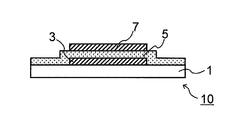
- the capacitor 10 may be configured by sandwiching the dielectric film 5 between the two electrodes 3 and 7 (in the embodiment (parallel plate type) shown in FIG. 1, the electrodes 3 and 7 are , Can be individually connected to leader wires at appropriate locations in the depth direction (not shown).
- a capacitor may be formed by providing a dielectric film straddling two electrodes existing apart from each other.
- the capacitor manufacturing method of the present embodiment may be manufactured by any suitable method, but can be typically carried out including the dielectric film manufacturing method described in detail in the first embodiment.
- the lower electrode 3, the dielectric film 5, and the upper electrode 7 may be sequentially laminated and formed on the surface of the substrate 1 to manufacture the capacitor 10.
- two electrodes may be formed on the surface of the substrate so as to be separated from each other, and a dielectric film may be formed so as to straddle them to manufacture a capacitor.
- the method for forming the dielectric film corresponds to the manufacturing method detailed in the first embodiment, and the method for forming the electrode may be any known suitable method.
- the conductive materials constituting the electrodes are, for example, Pt, Ti, W, Al, Ni, Ag, Au, Pd, Ir, Rh, TiC, TaC, TiN, Ag 2 O, Ru, Ru 2 O, SrRuO 3 , Nb. It may be added SrTiO 3, or the like, and may be, for example, one layer or a laminate of two or more layers.
- the material constituting the substrate is not particularly limited, for example Si, or and the like oxide single crystals such as SrTiO 3. Any suitable material layer, such as the SiO 2 layer, may be present between the substrate and the electrodes.
- the capacitor of the present embodiment has the same effect as the dielectric film described in detail in the first embodiment.
- the surface of the electrode in contact with the dielectric film is preferably the surface of (111) or (001), for example. More specifically, when the electrode is made of a crystalline material, the preferred orientation exhibited by the surface of the electrode may differ depending on the crystal structure of the crystalline material. For example, at least according crystallinity material, cubic material (e.g. Pt, W, Al, Ni, Ag, Au, Pd, Ir, Rh, TiC, TaC, is selected from the group consisting of TiN and Ag 2 O, etc. If it is one), if a tetragonal materials (e.g. Ru 2 O, etc.), or is a perovskite oxide (cubic) (e.g.
- Example 1 This embodiment relates to a dielectric film having a composition represented by (Sr x La 1-x ) 2 (Ta x Ti 1-x ) 2 O 7 and a capacitor including such a dielectric film.
- a Si (100) substrate having a SiO 2 film with a thickness of about 300 nm on its surface is prepared, and a Ti layer with a thickness of about 10 nm and a thickness of about 100 nm are formed on the surface by DC sputtering.
- the Pt layers were sequentially laminated to form a lower electrode composed of these layers.
- the temperature of the substrate was set to room temperature (about 20 ° C.).
- the Ti layer was provided as a relatively thin layer in order to improve the adhesion between the SiO 2 film and the Pt layer.
- the Pt layer is the main body portion of the lower electrode, whereby the electrode surface of the (111) plane is formed.
- the substrate on which the lower electrode is formed as described above is heated to 400 ° C. (that is, the substrate temperature is 400 ° C.), and then RF sputtering is performed on the substrate (Sr x La 1-).
- x ) 2 (Ta x Ti 1-x ) A precursor film having a composition represented by 2 O 7 was formed (note that a part (end) of the lower electrode did not form a precursor on it. I left it exposed).
- RF sputtering uses the target of the Sr 2 Ta 2 O 7 raw material and the target of the La 2 Ti 2 O 7 raw material as the vapor deposition source, and determines the RF power ratio of the Sr 2 Ta 2 O 7 raw material: La 2 Ti 2 O 7 raw material. It was vapor-deposited at the same time as 20W: 60W. The oxygen concentration in the ambient atmosphere of the substrate was 5%.
- the substrate on which the precursor film was formed as described above is subjected to heat treatment at 900 ° C. for 5 minutes while oxygen gas is allowed to flow at 0.5 L / min. (I.e., PDA temperature 900 ° C.), a dielectric film having a composition represented by (Sr x La 1-x ) 2 (Ta x Ti 1-x ) 2 O 7 is formed from the precursor film. did.
- the thickness of the obtained dielectric film was about 200 nm.
- a Pt layer having a thickness of about 150 nm was formed as an upper electrode in a substantially circular shape having a diameter of about 110 nm by DC sputtering.
- the temperature of the substrate was set to room temperature (about 20 ° C.).
- room temperature about 20 ° C.
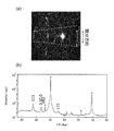
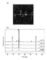
- FIG. 3A the results are shown in FIG. 3 (b).
- the symbol “*” indicates a peak caused by a substance other than the dielectric film (Pt, Ti, SiO 2 and Si) and is ignored because it does not constitute the dielectric film (described later).
- FIGS. 13 (b), 15 (b), 17 (b), 19 (b), 21, and 22), and the peak near 2 ⁇ 40 ° is due to Pt).
- the dielectric film of this example was compared with the known powder X-ray diffraction data (ICDD) of Sr 2 Ta 2 O 7 and La 2 Ti 2 O 7 (the following examples and comparative examples).
- ICDD powder X-ray diffraction data
- the known data used in the above are appropriately selected depending on the raw materials used as the deposition source), and it was identified that Sr 2 Ta 2 O 7 is the main component of the crystal structure.
- Orientation degree of orientation plane Each peak (however, peaks caused by substances other than the dielectric film are excluded) was fitted by a Gaussian function from the X-ray diffraction pattern (one-dimensional profile) of the dielectric film obtained above. The results are shown in FIG. 4 (in the figure, the measurement data of the one-dimensional profile is shown by a solid line, and the data fitted by the Gaussian function is shown by a dotted line). From this fitting, p was calculated by calculating the ratio of the diffraction intensity area of the peak of the orientation plane (111) to the sum of the diffraction intensity areas of all the peaks.
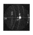
- the arc region including the spot of the orientation plane (111) of the two-dimensional X-ray diffraction image is set in the 2 ⁇ direction, in the dotted line region schematically shown in FIG. 5 (a).
- the integration was performed to obtain a one-dimensional profile, and the peak of the orientation plane (111) was fitted by a Gaussian function.
- FIG. 5 (b) in the figure, the measurement data of the one-dimensional profile is shown by a solid line, and the data (including the background) fitted by the Gaussian function is shown by a dotted line). From this fitting, the half width (°) of the peak of the orientation plane (111) was measured and found to be 6.42 °.
- the electrical characteristics of the dielectric film of this example were evaluated. More specifically, a DC voltage of 3 V is applied between the upper electrode and the lower electrode of the capacitor manufactured as described above, and the relative permittivity (-), the dielectric loss (-) and the dielectric loss (-) are applied at a measurement frequency of 1 MHz. The current density (A / cm 2 ) was measured. The results are shown in FIG. As can be understood from FIG. 6, the dielectric film of this embodiment exhibits a high relative permittivity exceeding 100 over 20 to 300 ° C., and the rate of change thereof is based on the relative permittivity at 20 ° C. It was less than 5%. Further, the dielectric film of this example showed a double-digit increase rate of the current density over 20 to 300 ° C., but showed a dielectric loss of less than 0.1 and functioned as a dielectric.
- Example 2 The present embodiment relates to a dielectric film having a composition represented by (Sr x La 1-x ) 2 (Nb x Ti 1-x ) 2 O 7 and a capacitor having such a dielectric film. Unless otherwise specified, the same description as in Example 1 applies (the same applies to the examples and comparative examples described in the present specification).
- step (a) the substrate was heated to 500 ° C. (that is, the substrate temperature was 500 ° C.), and RF sputtering used the target of the Sr 2 Nb 2 O 7 raw material and the La 2 Ti 2 O 7 raw material as the vapor deposition source.
- the RF power ratio of the Sr 2 Nb 2 O 7 raw material: La 2 Ti 2 O 7 raw material was set to 50 W: 60 W, and the film was simultaneously vapor-deposited to (Sr x La 1-x ) 2 (Nb x Ti 1-).
- Example 2 Example 2
- a dielectric film having a composition represented by (1) was formed to obtain a capacitor (the PDA temperature was set to 900 ° C. as in Example 1). The thickness of the obtained dielectric film was about 200 nm.
- FIG. 7 Main body and orientation plane of crystal structure A two-dimensional X-ray diffraction image of this dielectric film is shown in FIG.
- Sr 2 Nb 2 O 7 mainly forms the crystal structure of the X-ray diffraction pattern.
- orientation degree of orientation plane The orientation degree of the orientation plane (150) of this dielectric film was 0.68.
- Figure 8 shows the results of evaluation of the electrical characteristics of the dielectric film of this example.
- the dielectric film of this embodiment exhibits a high relative permittivity exceeding 100 over 20 to 150 ° C., and the rate of change thereof is based on the relative permittivity at 20 ° C. It was less than 5%.
- the dielectric film of this example showed high insulating properties having a current density of 1 ⁇ 10 -7 A / cm 2 or less and a dielectric loss of 0.05 or less.
- the dielectric film of this example had a large leakage current at a temperature exceeding 160 ° C., and its electrical characteristics were not evaluated.
- This comparative example relates to a dielectric film having a composition represented by (Sr x La 1-x ) 2 (Ta x Ti 1-x ) 2 O 7 and a capacitor having such a dielectric film.
- Tables show the heating temperature of the substrate in step (a), the RF power ratio of the Sr 2 Ta 2 O 7 raw material: La 2 Ti 2 O 7 raw material, and the heat treatment temperature (PDA temperature) in step (b).
- a dielectric film having a composition represented by (Sr x La 1-x ) 2 (Ta x Ti 1-x ) 2 O 7 in the same manner as in Example 1 except that they are different as shown in 2. was formed to obtain a capacitor. The thickness of the obtained dielectric film is also shown in Table 2.
- FIGS. 9 to 11 Two-dimensional X-ray diffraction images of the dielectric films of Comparative Examples 1 to 3 are shown in FIGS. 9 to 11, respectively.
- Sr 2 Ta 2 O 7 mainly forms the crystal structure.
- Orientation degree of orientation plane The orientation degree of the orientation plane (041) of the dielectric film of Comparative Example 1 was 0.66. Although the dielectric film of Comparative Example 2 was not an orientation plane, the degree of orientation of (080) was 0.065, and the degree of orientation of (010) was 0.22. The dielectric film of Comparative Example 3 was not an alignment plane, but the degree of orientation of (111) was 0.30.
- the dielectric film of Comparative Example 1 exhibited a relative permittivity of about 45 and a dielectric loss of about 0.05 at room temperature (about 20 ° C.).
- the dielectric film of Comparative Example 2 exhibited a relative permittivity of about 30 and a dielectric loss of about 0.05 at room temperature (about 20 ° C.).
- the dielectric film of Comparative Example 3 exhibited a relative permittivity of about 600 and a dielectric loss of about 0.05 at room temperature (about 20 ° C.).
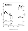
- Comparative Examples 1 to 3 were modified (each distance from the two vapor deposition sources was made different, etc.), and (Sr x La 1-x ) 2 (Ta x Ti 1-x ) 2 O 7 .
- the dielectric films and capacitors having different x in the formula were obtained, and the results of evaluating the electrical characteristics at room temperature (about 20 ° C.) are shown in FIG. 12 (in FIG. 12). indicating "xSr 2 Ta 2 O 7 - ( 1-x) La 2 Ti 2 O 7 " is a representation of the raw material base, (Sr x La 1-x ) 2 (Ta x Ti 1-x) 2 O 7 as synonymous). In each case, the relative permittivity was as low as less than 70.
- This comparative example relates to a dielectric film having a composition represented by Sr 2 Ta 2 O 7 and a capacitor including such a dielectric film.
- the substrate temperature was 500 ° C. and the PDA temperature was 900 ° C.
- the thickness of the obtained dielectric film was about 200 nm.
- the dielectric film of this comparative example has a composition of Sr 2 Ta 2 O 7 , and the element of A is only Sr.
- Sr 2 Ta 2 O 7 is the main component of the crystal structure.
- step (b) It is an X-ray diffraction pattern of the film after forming and before subjecting to step (b), and "700 ° C.” and “800 ° C.” set the heat treatment (PDA temperature) in step (b) to 700 ° C. It is an X-ray diffraction pattern of the obtained dielectric film. From FIG. 13B, it can be understood that a PDA temperature of 900 ° C. is required to bring about the orientation planes (110) and (200) by crystallization in this dielectric film.
- Orientation degree of alignment plane The orientation degree of the orientation plane (110) of the dielectric film of this comparative example was 0.81, and the orientation degree of the orientation plane (200) was 0.08.
- FIG. 14 shows the results of evaluation of the electrical characteristics of the dielectric film of this comparative example. As can be seen from FIG. 14, the dielectric film of this comparative example exhibited a low relative permittivity of about 45 to 55 over 20 to 300 ° C.
- This comparative example relates to a dielectric film having a composition represented by Sr 2 Nb 2 O 7 and a capacitor including such a dielectric film.
- a dielectric film having a composition represented by Sr 2 Nb 2 O 7 was formed in the same manner as in Example 1 except that a precursor film having a composition represented by 7 was formed to obtain a capacitor. (Similar to Example 1, the substrate temperature was 500 ° C. and the PDA temperature was 900 ° C.). The thickness of the obtained dielectric film was about 200 nm.
- the dielectric film of this comparative example has a composition of Sr 2 Nb 2 O 7 , and the element A is only Sr.
- Sr 2 Nb 2 O 7 is the main component of the crystal structure.
- the dielectric film of this comparative example has no orientation plane (in other words, the (131) plane and (in other words, the (131) plane) and ( 150) The plane is not an oriented plane).
- the X-ray diffraction pattern of the film obtained by modifying this comparative example is also shown in FIG. 15 (b), and “after film formation” indicates the precursor film of step (a). It is an X-ray diffraction pattern of the film after forming and before subjecting to step (b), and "700 ° C.” and "800 ° C.” set the heat treatment (PDA temperature) in step (b) to 700 ° C. and 800 ° C., respectively. It is an X-ray diffraction pattern of the obtained dielectric film.
- orientation degree of orientation plane Although the dielectric film of this comparative example is not an orientation plane, the orientation degree of (131) was 0.52 and the orientation degree of (150) was 0.30.
- Figure 16 shows the results of evaluation of the electrical characteristics of the dielectric film of this comparative example. As can be understood from FIG. 16, the dielectric film of this comparative example exhibited a low relative permittivity of about 40 to 60 over 20 to 300 ° C.
- This comparative example relates to a dielectric film having a composition represented by La 2 Ti 2 O 7 and a capacitor including such a dielectric film.
- the RF sputtering, using La 2 Ti 2 O 7 raw material target as evaporation source, and the La 2 Ti 2 O 7 raw RF power deposited as 50W, La 2 Ti 2 O A capacitor was obtained by forming a dielectric film having a composition represented by La 2 Ti 2 O 7 in the same manner as in Example 1 except that a precursor film having a composition represented by 7 was formed.
- the substrate temperature was 500 ° C. and the PDA temperature was 900 ° C.
- the thickness of the obtained dielectric film was about 80 nm.
- the dielectric film of this comparative example has a composition of La 2 Ti 2 O 7 , and the element A is only La.
- La 2 Ti 2 O 7 mainly forms the crystal structure.
- the dielectric film of this comparative example does not have an orientation plane (in other words, the (400) plane is orientation. Not a face).
- the X-ray diffraction pattern of the film obtained by modifying this comparative example is also shown in FIG. 17 (b), and “after film formation” indicates the precursor film of step (a). It is an X-ray diffraction pattern of the film after forming and before subjecting to step (b), and "700 ° C.” and "800 ° C.” set the heat treatment (PDA temperature) in step (b) to 700 ° C. It is an X-ray diffraction pattern of the obtained dielectric film.
- orientation degree of orientation plane Although the dielectric film of this comparative example is not an orientation plane, the orientation degree of (400) was 0.534.
- This comparative example relates to a dielectric film having a composition represented by La 2 Zr 2 O 7 and a capacitor including such a dielectric film.
- the RF sputtering, using a La 2 Zr 2 O 7 raw material target as evaporation source, and the La 2 Zr 2 O 7 raw RF power deposited as 50W, La 2 Zr 2 O A capacitor was obtained by forming a dielectric film having a composition represented by La 2 Zr 2 O 7 in the same manner as in Example 1 except that a precursor film having a composition represented by 7 was formed.
- the substrate temperature was 500 ° C. and the PDA temperature was 900 ° C.
- the thickness of the obtained dielectric film was about 60 nm.
- the dielectric film of this comparative example has a composition of La 2 Zr 2 O 7 , and the element A is only La.
- La 2 Zr 2 O 7 mainly forms the crystal structure.
- the dielectric film of this comparative example was ( It was found to have an orientation plane of 222) (in other words, the (444) plane is not an orientation plane).
- the X-ray diffraction pattern of the film obtained by modifying this comparative example is also shown in FIG. 18 (b), and “after film formation” indicates the precursor film of step (a). It is an X-ray diffraction pattern of the film after forming and before subjecting to step (b), and "700 ° C.” and "800 ° C.” set the heat treatment (PDA temperature) in step (b) to 700 ° C. It is an X-ray diffraction pattern of the obtained dielectric film.
- Orientation degree of orientation plane In the dielectric film of this comparative example, the orientation degree of the orientation plane (222) was 0.97.
- This comparative example relates to a dielectric film having a composition represented by Sr 2 (Ta x Nb 1-x ) 2 O 7 and a capacitor including such a dielectric film.
- RF sputtering uses a target of Sr 2 Ta 2 O 7 raw material and a target of Sr 2 Nb 2 O 7 raw material as a vapor deposition source, and Sr 2 Ta 2 O 7 raw material: Sr 2 Nb.
- the RF power ratio of the 2 O 7 raw material is 50 W: 50 W
- the opening area is alternately vapor-deposited via a controllable shutter mechanism to obtain a composition represented by Sr 2 (Ta x Nb 1-x ) 2 O 7.
- a capacitor was obtained by forming a dielectric film having a composition represented by Sr 2 (Ta x Nb 1-x ) 2 O 7 in the same manner as in Example 1 except that the precursor film having the precursor film was formed. (Similar to Example 1, the substrate temperature was 500 ° C. and the PDA temperature was 900 ° C.). The thickness of the obtained dielectric film was about 70 nm.
- the composition can be inclined in the dielectric film, which is generally close to the Sr 2 Ta 2 O 7 raw material. The region became Sr 2 Ta 2 O 7 rich, and the region close to the Sr 2 Nb 2 O 7 raw material became Sr 2 Nb 2 O 7 rich.
- xSr 2 Ta 2 O 7 - ( 1-x) Sr 2 Nb 2 O 7 is a representation of the raw material base, synonymous with Sr 2 (Ta x Nb 1- x) 2 O 7 Is).
- the relative permittivity at room temperature (25 ° C.) is 60 or less, which is a high relative permittivity. Was not obtained.
- This comparative example relates to a dielectric film having a composition represented by La 2 (Zr x Ti 1-x ) 2 O 7 and a capacitor including such a dielectric film.
- step (a) the substrate was heated to 550 ° C (that is, the substrate temperature was 550 ° C), and RF sputtering was performed as a vapor deposition source for the target of the La 2 Zr 2 O 7 raw material and the La 2 Ti 2 O 7 raw material.
- RF sputtering was performed as a vapor deposition source for the target of the La 2 Zr 2 O 7 raw material and the La 2 Ti 2 O 7 raw material.
- La 2 Zr 2 O 7 raw material La 2 Ti 2 O 7 raw RF power ratio of the 50 W: as 50 W
- by depositing alternately via a controllable shutter mechanism opening area La 2 ( Zr x Ti 1-x ) La 2 (Zr x Ti 1-x ) 2 O 7 in the same manner as in Example 1 except that a precursor film having a composition represented by 2 O 7 was formed.
- a dielectric film having the composition to be obtained was formed to obtain a capacitor (the PDA temperature was set to 900 ° C. as in Example 1). The
- the composition gradient can be generated in the dielectric film, and is generally close to the La 2 Zr 2 O 7 raw material. The region became La 2 Zr 2 O 7 rich, and the region close to the La 2 Ti 2 O 7 raw material became La 2 Ti 2 O 7 rich.
- xLa 2 Zr 2 O 7 - ( 1-x) La 2 Ti 2 O 7 is a representation of the raw material base, La 2 (Zr x Ti 1 -x) 2 O 7 as defined Is).
- x 1.0, the dielectric film of Comparative Example 7 had an orientation plane (222).
- Comparative Examples 6 and 7 have a substrate temperature of 500 ° C., unlike this Comparative Example.
- X 0, 0.2, 0.4, 0.6, 0.8 and 1
- the relative permittivity at room temperature (25 ° C.) was 50 or less, and a high relative permittivity could not be obtained.
- the leakage current exceeded 1 mA at 50 ° C. or higher, and the electrical characteristics could not be evaluated.
- the dielectric film of the present invention is suitably used as a dielectric film in a capacitor (particularly a thin film capacitor), and such a capacitor can be used for various electronic components, but the dielectric film of the present invention is not limited to such applications. ..
Abstract
Provided is a dielectric film capable of stably maintaining a high dielectric constant across a wide temperature range (e.g., 20–150°C). The dielectric film has a pyrochlore or layered perovskite crystalline structure having a composition indicated by general formula A2B2O7 (in the formula, A indicates at least two elements (mutually different A1 and A2) selected from the group consisting of Mg, Ca, Sr, Ba, La, Ce, Pr, Nd, Pm, Sm, Eu, Gd, Tb, Dy, Ho, Er, Tm, Yb, and Lu and B includes at least one element (B1) selected from the group consisting of Ti, Zr, Hf, V, Nb, and Ta.) A1
2B1
2O7, which is the main component of the crystalline structure of the dielectric film, has at least one orientation plane in addition to (h00), (0k0), (00l), (h0l), and (0kl) planes (h, k, and l are integers other than 0).
Description
本発明は、誘電体膜およびそれを用いたキャパシタ、ならびにかかる誘電体膜の製造方法に関する。
The present invention relates to a dielectric film, a capacitor using the same, and a method for manufacturing such a dielectric film.
従前、フローティングゾーン法で成長させた一般式A2B2O7で表される組成(例えばSr2Ta2O7、Sr2Nb2O7等)を有する単結晶(これは薄膜と区別して「バルク単結晶」とも呼ばれる)が、誘電性を示すことが報告されている(非特許文献1参照)。この報告に関連して、フローティングゾーン法で得たSr2Ta2O7の結晶構造は、Sr2Nb2O7の結晶構造と同じく、ペロブスカイト型スラブ構造であるという報告も存在する(非特許文献2参照)。
Previously, a single crystal having a composition represented by the general formula A 2 B 2 O 7 grown by the floating zone method (for example, Sr 2 Ta 2 O 7 , Sr 2 Nb 2 O 7 etc.) (this is distinguished from a thin film). (Also referred to as "bulk single crystal") has been reported to exhibit dielectric properties (see Non-Patent Document 1). In connection with this report, there is also a report that the crystal structure of Sr 2 Ta 2 O 7 obtained by the floating zone method is a perovskite type slab structure similar to the crystal structure of Sr 2 Nb 2 O 7 (non-patent). Reference 2).
更に、パイロクロア型の結晶構造を有し、かつ一般式A2B2O7で表される組成(例えばSr2Ta2O7等)を有する誘電体膜が、2つの電極間に配置されたキャパシタ(薄膜コンデンサ)が知られている(特許文献1参照)。特許文献1には、パイロクロア型化合物であるSr2Ta2O7からなる誘電体膜をCVD法により基板温度400℃で形成したところ、600の比誘電率を示したことが記載されている。
Further, a dielectric film having a pyrochlore-type crystal structure and a composition represented by the general formula A 2 B 2 O 7 (for example, Sr 2 Ta 2 O 7 or the like) was arranged between the two electrodes. Capacitors (thin film capacitors) are known (see Patent Document 1). Patent Document 1 describes that a dielectric film made of Sr 2 Ta 2 O 7 , which is a pyrochlore-type compound, was formed by a CVD method at a substrate temperature of 400 ° C. and exhibited a relative permittivity of 600.
また、(Sr2Ta2O7)100-x(La2Ti2O7)x(式中、0≦x≦5)で表される組成を有する層状ペロブスカイト材料であって、対応する金属酸化物粉末原料を用いた2段階固相反応によりペレット状(直径12または18mm、厚さ0.5mm)に作製した材料も知られている(非特許文献3参照)。この材料は、20~300℃の温度範囲において比誘電率が大きく変化することが報告されている(非特許文献3の図7参照)。
Further, a layered perovskite material having a composition represented by (Sr 2 Ta 2 O 7 ) 100-x (La 2 Ti 2 O 7 ) x (in the formula, 0 ≦ x ≦ 5), and corresponding metal oxidation. A material prepared in the form of pellets (diameter 12 or 18 mm, thickness 0.5 mm) by a two-step solid phase reaction using a material powder raw material is also known (see Non-Patent Document 3). It has been reported that the relative permittivity of this material changes significantly in the temperature range of 20 to 300 ° C. (see FIG. 7 of Non-Patent Document 3).
電子部品等に利用されるキャパシタは、広い温度範囲、例えば20℃程度の室温または常温から150℃程度の比較的高温、好ましくは300℃程度の高温までの範囲に亘って、安定した電気特性を示すことが求められ、なかでも、かかる温度範囲に亘って高い比誘電率を安定的に維持することが望ましい。しかしながら、上述した従来のキャパシタや材料では、かかる温度範囲に亘って高い比誘電率を安定的に維持できないことが、本発明者らの研究により判明した。
Capacitors used for electronic components, etc. have stable electrical characteristics over a wide temperature range, for example, room temperature of about 20 ° C. or relatively high temperature of about normal temperature to about 150 ° C., preferably high temperature of about 300 ° C. It is required to show, and above all, it is desirable to stably maintain a high relative permittivity over such a temperature range. However, it has been found by the studies of the present inventors that the above-mentioned conventional capacitors and materials cannot stably maintain a high relative permittivity over such a temperature range.
本発明は、広い温度範囲(例えば20~150℃)に亘って、高い比誘電率を安定的に維持し得る誘電体膜およびそれを用いたキャパシタ、ならびにかかる誘電体膜の製造方法を提供することを目的とする。
The present invention provides a dielectric film capable of stably maintaining a high relative permittivity over a wide temperature range (for example, 20 to 150 ° C.), a capacitor using the same, and a method for producing such a dielectric film. The purpose is.
本発明者らは、一般式A2B2O7で表される組成を有する誘電体膜の配向面を制御するという独自の着想を得、更なる鋭意研究の結果、本発明を完成するに至った。
The present inventors have obtained an original idea of controlling the orientation plane of a dielectric film having a composition represented by the general formula A 2 B 2 O 7 , and have completed the present invention as a result of further diligent research. I arrived.
本発明の1つの要旨によれば、パイロクロア型または層状ペロブスカイト型の結晶構造を有する誘電体膜であって、
一般式A2B2O7(式中、Aは、Mg、Ca、Sr、Ba、La、Ce、Pr、Nd、Pm、Sm、Eu、Gd、Tb、Dy、Ho、Er、Tm、YbおよびLuからなる群より選択される2つ以上の元素であって、このうち各1つの元素として互いに異なるA1およびA2を含み、Bは、Ti、Zr、Hf、V、NbおよびTaからなる群より選択される1つ以上の元素であって、このうち1つの元素としてB1を含む)で表される組成を有し、
該誘電体膜中に存在するAおよびBの元素から各1つを選択して化学量論的に得られるA2B2O7の全ての組合せのうち、該誘電体膜の結晶構造の主体を成すA1 2B1 2O7に関して、(h00)、(0k0)、(00l)、(h0l)および(0kl)の面(h、kおよびlは0を除く整数である)以外に、少なくとも1つの配向面を有する、誘電体膜が提供される。 According to one gist of the present invention, a dielectric film having a pyrochlore-type or layered perovskite-type crystal structure.
General formula A 2 B 2 O 7 (In the formula, A is Mg, Ca, Sr, Ba, La, Ce, Pr, Nd, Pm, Sm, Eu, Gd, Tb, Dy, Ho, Er, Tm, Yb. Two or more elements selected from the group consisting of and Lu, each containing A 1 and A 2 different from each other, where B is from Ti, Zr, Hf, V, Nb and Ta. and one or more elements selected from the group consisting having a composition represented by the among containing B 1 as one element),
Of all the combinations of A 2 B 2 O 7 obtained stoichiometrically by selecting one of each of the elements A and B existing in the dielectric film, the main component of the crystal structure of the dielectric film. With respect to A 1 2 B 1 2 O 7 forming the above, in addition to the faces (h00), (0k0), (00l), (h0l) and (0kl) (h, k and l are integers excluding 0). A dielectric film having at least one orientation plane is provided.
本発明のもう1つの要旨によれば、電極と、該電極の上に配置された上記本発明の誘電体膜とを含むキャパシタが提供される。
According to another gist of the present invention, a capacitor including an electrode and the dielectric film of the present invention arranged on the electrode is provided.
本発明も更にもう1つの要旨によれば、パイロクロア型または層状ペロブスカイト型の結晶構造を有する誘電体膜の製造方法であって、
(a)350~600℃の温度に加熱された基板の表面に、一般式A2B2O7(式中、Aは、Mg、Ca、Sr、Ba、La、Ce、Pr、Nd、Pm、Sm、Eu、Gd、Tb、Dy、Ho、Er、Tm、YbおよびLuからなる群より選択される2つ以上の元素であって、このうち各1つの元素として互いに異なるA1およびA2を含み、Bは、Ti、Zr、Hf、V、NbおよびTaからなる群より選択される1つ以上の元素であって、このうち1つの元素としてB1を含む)で表される組成を有する前駆体膜を気相堆積により形成すること、および
(b)前記前駆体膜が形成された前記基板を、酸素を含む雰囲気にて850~1050℃の温度で熱処理して、該前駆体膜から、パイロクロア型または層状ペロブスカイト型の結晶構造を有し、かつ前記組成を有する誘電体膜を得ること
を含む、製造方法が提供される。 According to yet another gist of the present invention, it is a method for producing a dielectric film having a pyrochlore-type or layered perovskite-type crystal structure.
(A) On the surface of the substrate heated to a temperature of 350 to 600 ° C., the general formula A 2 B 2 O 7 (in the formula, A is Mg, Ca, Sr, Ba, La, Ce, Pr, Nd, Pm. , Sm, Eu, Gd, Tb, Dy, Ho, Er, Tm, Yb and Lu, two or more elements selected from the group, each of which is different from each other, A 1 and A 2. B is one or more elements selected from the group consisting of Ti, Zr, Hf, V, Nb and Ta, and B 1 is included as one of the elements). The precursor film to have is formed by vapor phase deposition, and (b) the substrate on which the precursor film is formed is heat-treated at a temperature of 850 to 1050 ° C. in an atmosphere containing oxygen to form the precursor film. To provide a production method comprising obtaining a dielectric film having a pyrochlore-type or layered perovskite-type crystal structure and having the above composition.
本発明によれば、パイロクロア型または層状ペロブスカイト型の結晶構造を有する誘電体膜において、一般式A2B2O7で表される組成を成すAサイトの元素が少なくとも2つ存在し、更に、該誘電体膜の結晶構造の主体を成すA1
2B1
2O7に関して、(h00)、(0k0)、(00l)、(h0l)および(0kl)の面(h、kおよびlは0を除く整数である)以外に、少なくとも1つの配向面を有することによって、広い温度範囲(例えば20~150℃)に亘って、高い比誘電率を安定的に維持し得る誘電体膜が提供される。更に、本発明によれば、かかる誘電体膜を用いたキャパシタ、ならびにかかる誘電体膜の製造方法も提供される。
According to the present invention, in a dielectric film having a pyrochloroa type or layered perovskite type crystal structure, at least two elements of A site having a composition represented by the general formula A 2 B 2 O 7 are present, and further. With respect to A 1 2 B 1 2 O 7 which is the main component of the crystal structure of the dielectric film, the planes (h, k and l) of (h00), (0k0), (00l), (h0l) and (0kl) are 0. By having at least one orientation plane in addition to (an integer excluding), a dielectric film capable of stably maintaining a high relative permittivity over a wide temperature range (for example, 20 to 150 ° C.) is provided. To. Further, according to the present invention, a capacitor using such a dielectric film and a method for producing such a dielectric film are also provided.
(実施形態1:誘電体膜およびその製造方法)
本発明の1つの実施形態によれば、誘電体膜およびその製造方法が提供される。 (Embodiment 1: Dielectric film and its manufacturing method)
According to one embodiment of the present invention, a dielectric film and a method for producing the same are provided.
本発明の1つの実施形態によれば、誘電体膜およびその製造方法が提供される。 (Embodiment 1: Dielectric film and its manufacturing method)
According to one embodiment of the present invention, a dielectric film and a method for producing the same are provided.
本実施形態の誘電体膜は、
パイロクロア型または層状ペロブスカイト型の結晶構造を有し、
一般式A2B2O7(式中、Aは、Mg、Ca、Sr、Ba、La、Ce、Pr、Nd、Pm、Sm、Eu、Gd、Tb、Dy、Ho、Er、Tm、YbおよびLuからなる群より選択される2つ以上の元素であって、このうち各1つの元素として互いに異なるA1およびA2を含み、Bは、Ti、Zr、Hf、V、NbおよびTaからなる群より選択される1つ以上の元素であって、このうち1つの元素としてB1を含む)で表される組成を有し、
該誘電体膜中に存在するAおよびBの元素から各1つを選択して化学量論的に得られるA2B2O7の全ての組合せのうち、該誘電体膜の結晶構造の主体を成すA1 2B1 2O7に関して、(h00)、(0k0)、(00l)、(h0l)および(0kl)の面(h、kおよびlは0を除く整数である)以外に、少なくとも1つの配向面を有する。 The dielectric film of this embodiment is
It has a pyrochlore-type or layered perovskite-type crystal structure.
General formula A 2 B 2 O 7 (In the formula, A is Mg, Ca, Sr, Ba, La, Ce, Pr, Nd, Pm, Sm, Eu, Gd, Tb, Dy, Ho, Er, Tm, Yb. Two or more elements selected from the group consisting of and Lu, each containing A 1 and A 2 different from each other, where B is from Ti, Zr, Hf, V, Nb and Ta. and one or more elements selected from the group consisting having a composition represented by the among containing B 1 as one element),
Of all the combinations of A 2 B 2 O 7 obtained stoichiometrically by selecting one of each of the elements A and B existing in the dielectric film, the main constituent of the crystal structure of the dielectric film. With respect to A 1 2 B 1 2 O 7 forming, other than the faces (h00), (0k0), (00l), (h0l) and (0kl) (h, k and l are integers excluding 0). It has at least one orientation plane.
一般式A2B2O7で表される組成を有する酸化物の結晶構造は、通常、パイロクロア型または層状ペロブスカイト型(ペロブスカイト型スラブとも称される)であり得る(これらの多形を採り得る場合も含む)。しかしながら、上記酸化物がどのような結晶構造となるかは、その具体的な組成および製造方法等によって異なり得、更に、上記酸化物が曝される温度および圧力等の条件によっても変化(例えば相変化および/または多形間で転移)し得る。よって、本発明において「パイロクロア型または層状ペロブスカイト型の結晶構造」とは、これらのいずれか一方または双方であってよい結晶構造を意味するものであり、いずれか一方のみに限定して解釈されない。
The crystal structure of the oxide having the composition represented by the general formula A 2 B 2 O 7 can usually be a pyrochlore type or a layered perovskite type (also referred to as a perovskite type slab) (these polymorphs can be adopted). Including cases). However, what kind of crystal structure the oxide has may differ depending on its specific composition, production method, etc., and further changes depending on conditions such as temperature and pressure to which the oxide is exposed (for example, phase). Can change and / or transfer between polymorphs). Therefore, in the present invention, the "pyrochlore-type or layered perovskite-type crystal structure" means a crystal structure that may be either one or both of them, and is not construed as being limited to only one of them.
本実施形態の誘電体膜は、一般式A2B2O7で表される組成を有する。AおよびBは、パイロクロア型または層状ペロブスカイト型の結晶構造においてそれぞれAサイトおよびBサイトを占める元素を意味する(または総称する)記号である。
The dielectric film of the present embodiment has a composition represented by the general formula A 2 B 2 O 7 . A and B are symbols that mean (or generically) the elements that occupy the A site and the B site, respectively, in the pyrochlore type or layered perovskite type crystal structure.
Aは、Mg、Ca、Sr、Ba、La、Ce、Pr、Nd、Pm、Sm、Eu、Gd、Tb、Dy、Ho、Er、Tm、YbおよびLuからなる群より選択される2つ以上の元素を含む。好ましくは、Aは、Sr、Ba、LaおよびNdからなる群より選択される2つ以上の元素を含む。Aに該当する具体的な元素は2つ以上存在し、これらをA1およびA2(これらは互いに異なる)として表記する。
A is two or more selected from the group consisting of Mg, Ca, Sr, Ba, La, Ce, Pr, Nd, Pm, Sm, Eu, Gd, Tb, Dy, Ho, Er, Tm, Yb and Lu. Contains the elements of. Preferably, A comprises two or more elements selected from the group consisting of Sr, Ba, La and Nd. There are two or more specific elements that correspond to A, and these are referred to as A 1 and A 2 (these are different from each other).
Bは、Ti、Zr、Hf、V、NbおよびTaからなる群より選択される1つ以上の元素を含む。好ましくは、Bは、Ti、NbおよびTaからなる群より選択される1つ以上の元素を含む。Bに該当する具体的な元素は1つ以上存在し、これをB1として表記する(なお、後述するB2もBに該当する具体的な元素であるが、B2はB1と同じであっても異なっていてもよい)。
B comprises one or more elements selected from the group consisting of Ti, Zr, Hf, V, Nb and Ta. Preferably, B comprises one or more elements selected from the group consisting of Ti, Nb and Ta. There is one or more specific elements corresponding to B, and this is referred to as B 1 (Note that B 2 described later is also a specific element corresponding to B, but B 2 is the same as B 1 . It may or may not be different).
A2B2O7は、化学量論的には、例えば、Aが3価の価数を採る元素であり、Bが4価の価数を採る元素である場合(すなわちA(III)2B(IV)2O7型)、Aが2価の価数を採る元素であり、Bが5価の価数を採る元素である場合(すなわちA(II)2B(V)2O7型)、ならびにこれらが混在している場合等であり得る。
Stoichiometrically, A 2 B 2 O 7 is, for example, when A is an element having a trivalent valence and B is an element having a tetravalent valence (that is, A (III) 2 ). B (IV) 2 O 7 type), when A is an element having a divalent valence and B is an element having a pentavalent valence (that is, A (II) 2 B (V) 2 O 7 ) Type), and when these are mixed, etc.
誘電体膜中に存在するAおよびBの元素から各1つを選択して化学量論的に得られる(または想定され得る)A2B2O7の全ての組合せのうち、誘電体膜の結晶構造の主体を成すA1
2B1
2O7を同定し、これによりA1およびB1の各元素が具体的に決定される。すなわち、本実施形態の誘電体膜において、A1
2B1
2O7が結晶構造の主体を成し、これにA2および存在し得る他の元素が固溶しているものと理解され得る。
Of all the combinations of A 2 B 2 O 7 obtained (or conceivable) stoichiometrically by selecting one of each of the elements A and B present in the dielectric film, the dielectric film A 1 2 B 1 2 O 7 which is the main component of the crystal structure is identified, and each element of A 1 and B 1 is specifically determined by this. That is, in the dielectric film of the present embodiment, it can be understood that A 1 2 B 1 2 O 7 forms the main body of the crystal structure, and A 2 and other elements that may exist are dissolved therein. ..
本発明において、A1
2B1
2O7が誘電体膜の「結晶構造の主体を成す」とは、A1
2B1
2O7が誘電体膜の結晶構造を主として担っていることを意味する。A2B2O7の全ての組合せのうち、どれが「結晶構造の主体を成す」A1
2B1
2O7であるかは、誘電体膜から得られるX線回折パターンに基づいて、誘電体膜の結晶構造に最も近い結晶構造を示すものとして決定される。
In the present invention, A 1 2 B 1 2 O 7 "forms the main body of the crystal structure" of the dielectric film means that A 1 2 B 1 2 O 7 mainly bears the crystal structure of the dielectric film. means. Which of all the combinations of A 2 B 2 O 7 is "mainly responsible for the crystal structure" A 1 2 B 1 2 O 7 is determined based on the X-ray diffraction pattern obtained from the dielectric film. It is determined to show the crystal structure closest to the crystal structure of the dielectric film.
例えば、A2B2O7が(SrxLa1-x)2(TaxTi1-x)2O7(式中、0<x<1)である誘電体膜の場合、Aに該当するSrおよびLaと、Bに該当するTaおよびTiとから各1つを選択して化学量論的に得られる全ての組合せは、Sr2Ta2O7およびLa2Ti2O7である(これら元素(価数)は、Sr(II)、La(III)、Ta(V)、Ti(IV)であることに留意されたい)。これらSr2Ta2O7およびLa2Ti2O7のうちいずれが「結晶構造の主体を成す」かは、誘電体膜から得られるX線回折パターンと、Sr2Ta2O7およびLa2Ti2O7の各々について既知の粉末X線回折データとを比較して、誘電体膜のX線回折パターンに最も近い粉末X線回折データに対応するもの(例えばSr2Ta2O7)を、結晶構造の主体を成すA1
2B1
2O7(例えばA1がSrであり、B1がTaである)として同定する。
For example, in the case of a dielectric film in which A 2 B 2 O 7 is (Sr x La 1-x ) 2 (Ta x Ti 1-x ) 2 O 7 (in the formula, 0 <x <1), it corresponds to A. All combinations obtained stoichiometrically by selecting one each of Sr and La corresponding to B and Ta and Ti corresponding to B are Sr 2 Ta 2 O 7 and La 2 Ti 2 O 7 ( Note that these elements (valences) are Sr (II), La (III), Ta (V), Ti (IV)). Which of these Sr 2 Ta 2 O 7 and La 2 Ti 2 O 7 "forms the main body of the crystal structure" depends on the X-ray diffraction pattern obtained from the dielectric film and Sr 2 Ta 2 O 7 and La 2 By comparing the known powder X-ray diffraction data for each of Ti 2 O 7 , the one corresponding to the powder X-ray diffraction data closest to the X-ray diffraction pattern of the dielectric film (for example, Sr 2 Ta 2 O 7 ) is obtained. , A 1 2 B 1 2 O 7 (for example, A 1 is Sr and B 1 is Ta) which form the main body of the crystal structure.
既知の粉末X線回折データは、例えばICDD(International Centre for Diffraction Data)等が提供しているデータベースから取得して利用することができる。誘電体膜のX線回折パターンには、2次元検出器を用いて得られる2次元X線回折像を1次元プロファイルに変換したもの(検出角度χ=38°の領域についてχ方向に円弧積分して変換することが好ましい)を利用してよく、同定に際しては、誘電体膜以外の物質(例えば誘電体膜の下地を成す物質、具体的には基板や存在する場合には電極用導電性部材)に起因するピークを無視する必要があり、更に、後述する配向面を考慮することが好ましい。これらの説明は、以下の説明においても特に断りのない限り同様に当て嵌まる。
Known powder X-ray diffraction data can be obtained and used from a database provided by, for example, ICDD (International Center for Diffraction Data). The X-ray diffraction pattern of the dielectric film is obtained by converting a two-dimensional X-ray diffraction image obtained by using a two-dimensional detector into a one-dimensional profile (arc integration in the χ direction in a region of a detection angle χ = 38 °). In the identification, a substance other than the dielectric film (for example, a substance forming the base of the dielectric film, specifically, a substrate or a conductive member for an electrode if present) may be used. ), It is necessary to ignore the peak, and it is preferable to consider the orientation plane described later. These explanations also apply to the following explanations in the same manner unless otherwise specified.
本発明において、誘電体膜の「配向面」とは、誘電体膜の表面に平行な面であって、配向性すなわち結晶性の高い面を意味し、より詳細には、2次元X線回折像においてスポット状に観察される面であり、その面指数(ミラー指数)は、結晶構造の主体を成すA1
2B1
2O7に関して決定される。本実施形態の誘電体膜は、かかる配向面を1つまたは2つ以上有していてよいが、誘電体膜の結晶構造の主体を成すA1
2B1
2O7に関して、(h00)、(0k0)、(00l)、(h0l)および(0kl)の面(h、kおよびlは0を除く整数である)以外に、少なくとも1つの配向面を有する。
In the present invention, the "alignment plane" of the dielectric film means a plane parallel to the surface of the dielectric film, which is highly oriented, that is, highly crystalline, and more specifically, two-dimensional X-ray diffraction. It is a surface observed in a spot shape in an image, and its surface index (Miller index) is determined with respect to A 1 2 B 1 2 O 7 which is the main component of the crystal structure. The dielectric film of the present embodiment, such alignment surface may have one or more, but with respect to A 1 2 B 1 2 O 7 constituting the main body of the crystal structure of the dielectric film, (h00), In addition to the planes (0k0), (00l), (h0l) and (0kl) (h, k and l are integers excluding 0), it has at least one orientation plane.
例えば、結晶構造の主体を成すA1
2B1
2O7がSr2Ta2O7である場合、誘電体膜の2次元X線回折像において観察される1つまたは2つ以上であってよいスポットの回折角度(2θ)を測定し、上記スポットの回折角度(2θ)が、A1
2B1
2O7であるSr2Ta2O7について既知の粉末X線回折データにおいてどの面に一致するかを調べることにより、上記スポットとして観察される1つまたは2つ以上の配向面の面指数が決定され。このようにして決定される少なくとも1つの配向面の面指数が、A1
2B1
2O7であるSr2Ta2O7の(h00)、(0k0)、(00l)、(h0l)および(0kl)の面(h、kおよびlは0を除く整数である)以外であればよい。上記スポットの回折角度(2θ)は、2次元X線回折像を変換して得られる1次元プロファイル(検出角度χ=38°の領域についてχ方向に円弧積分して変換することが好ましい)を用いて、上記スポットに対応するピークに基づいて測定してよい。
For example, when A 1 2 B 1 2 O 7 which forms the main body of the crystal structure is Sr 2 Ta 2 O 7, it is one or more observed in the two-dimensional X-ray diffraction image of the dielectric film. The diffraction angle (2θ) of a good spot is measured, and on which surface in the powder X-ray diffraction data known for Sr 2 Ta 2 O 7 that the diffraction angle (2θ) of the spot is A 1 2 B 1 2 O 7. By examining the coincidence, the plane index of one or more oriented planes observed as the spot is determined. The plane index of at least one orientation plane thus determined is (h00), (0k0), (00l), (h0l) and (h0l) of Sr 2 Ta 2 O 7 of A 1 2 B 1 2 O 7. Any surface other than the plane (0 kl) (h, k and l are integers excluding 0) may be used. The diffraction angle (2θ) of the spot uses a one-dimensional profile obtained by converting a two-dimensional X-ray diffraction image (preferably, the region of the detection angle χ = 38 ° is converted by arc integration in the χ direction). The measurement may be performed based on the peak corresponding to the spot.
本実施形態の誘電体膜は、その結晶構造の主体を成すA1
2B1
2O7に関して、(h00)、(0k0)、(00l)、(h0l)および(0kl)の面(h、kおよびlは0を除く整数である)以外に、少なくとも1つの配向面を有する。これは、誘電体膜の表面に対して、誘電体膜を成す結晶のb軸方向が直交せずに傾いていることを意味する。
The dielectric film of the present embodiment has (h,), (0k0), (00l), (h0l) and (0kl) planes (h,) with respect to A 1 2 B 1 2 O 7 which is the main component of the crystal structure. In addition to (k and l are integers excluding 0), it has at least one orientation plane. This means that the b-axis direction of the crystals forming the dielectric film is not orthogonal to the surface of the dielectric film and is tilted.
本実施形態の誘電体膜は、上記のような配向面を有することによって、広い温度範囲(例えば20~150℃、好ましくは20~300℃)に亘って、高い比誘電率を安定的に、すなわち小さい変化率で維持することが可能となる。本発明はいかなる理論によっても拘束されないが、その理由は次のように考えられ得る。パイロクロア型または層状ペロブスカイト型の結晶構造を有する誘電体膜は、20~150℃の温度範囲、より広範には20~300℃の温度範囲において、a軸方向、b軸方向およびc軸方向の各比誘電率の大きさおよび温度依存性が異なる。より詳細には、誘電体膜の組成にもよるが、かかる温度範囲においては、a軸方向およびc軸方向の比誘電率は、b軸方向の誘電率に対して高く、安定した微増傾向を示すものの、a軸方向およびc軸方向のキュリー温度(非誘電率が急激に上昇してピークを示す温度)は、かかる温度範囲に対して相当離れた高い温度領域にあり、他方、b軸方向のキュリー温度は、かかる温度範囲に対してほど近い低い温度領域にある。このことから、誘電体膜の表面に対して結晶のb軸方向を傾けることによって、b軸方向の寄与による比誘電率の上昇を利用しつつ、a軸方向およびc軸方向の有する比誘電率の安定性を組み合わせることができると考えられる。かかる組合せの効果は、Aサイトの元素を2つ以上とした場合に顕著に生じ得ると考えられる。そこで、Aサイトの元素を2つ以上とし、結晶構造の主体を成すA1
2B1
2O7にA2および存在し得る他の元素を固溶させ、かつ、誘電体膜の表面に対して結晶のb軸方向を傾けることによって、20~150℃、好ましくは20~300℃の温度範囲においてより高くかつ安定した比誘電率を得ることが可能となると考えられる。
By having the orientation plane as described above, the dielectric film of the present embodiment stably maintains a high relative permittivity over a wide temperature range (for example, 20 to 150 ° C., preferably 20 to 300 ° C.). That is, it can be maintained at a small rate of change. The present invention is not bound by any theory, the reason for which can be considered as follows. A dielectric film having a pyrochlore-type or layered perovskite-type crystal structure is provided in the a-axis direction, the b-axis direction, and the c-axis direction in a temperature range of 20 to 150 ° C., more broadly, in a temperature range of 20 to 300 ° C. The magnitude of the relative permittivity and the temperature dependence are different. More specifically, although it depends on the composition of the dielectric film, in such a temperature range, the relative permittivity in the a-axis direction and the c-axis direction is higher than the permittivity in the b-axis direction, and a stable slight increase tendency is exhibited. Although shown, the Curie temperature in the a-axis direction and the c-axis direction (the temperature at which the non-dielectric constant rises sharply and shows a peak) is in a high temperature region considerably distant from such a temperature range, while in the b-axis direction. Curie temperature is in a low temperature range, not close to such a temperature range. From this, by tilting the b-axis direction of the crystal with respect to the surface of the dielectric film, the relative permittivity of the a-axis direction and the c-axis direction is utilized while utilizing the increase in the relative permittivity due to the contribution in the b-axis direction. It is thought that the stability of can be combined. It is considered that the effect of such a combination can be remarkably generated when two or more elements of A site are used. Therefore, the number of elements at the A site is two or more, and A 2 and other elements that may exist are dissolved in A 1 2 B 1 2 O 7 which is the main component of the crystal structure, and the surface of the dielectric film is By tilting the b-axis direction of the crystal, it is considered possible to obtain a higher and stable relative permittivity in the temperature range of 20 to 150 ° C., preferably 20 to 300 ° C.
本実施形態の誘電体膜の上記少なくとも1つの配向面は、結晶構造の主体を成すA1
2B1
2O7に関して、上述したように(h00)、(0k0)、(00l)、(h0l)および(0kl)の面以外であればよい。かかる少なくとも1つの配向面は、例えば(111)、(131)、(151)、(1 15 1)、(192)、(153)、(157)、(110)、(150)、(212)、(172)および(1 13 0)などのいずれか1つまたは2つ以上であってよいが、これに限定されない。なお、本明細書において、h、kおよびlが、いずれも1桁の整数である場合は(hkl)の表記に従って示すが、これらの少なくとも1つが2桁以上の整数である場合は、整数間にスペースを設けて示す。
The at least one orientation plane of the dielectric film of the present embodiment is (h00), (0k0), (00l), (h0l) as described above with respect to A 1 2 B 1 2 O 7 which is the main body of the crystal structure. ) And (0 kl) planes. Such at least one orientation plane is, for example, (111), (131), (151), (115 1), (192), (153), (157), (110), (150), (212). , (172) and (1 130), and the like, but not limited to any one or more. In the present specification, when h, k and l are all one-digit integers, they are shown according to the notation of (hkl), but when at least one of them is an integer of two or more digits, between integers. Is shown with a space.
更に、本実施形態の誘電体膜の上記少なくとも1つの配向面は、結晶構造の主体を成すA1
2B1
2O7に関して、上述した面以外で、かつ、(hk0)の面(h、kおよびlは0を除く整数である)以外の面であることが好ましい。これにより、誘電体膜の表面に対して結晶のb軸方向をより適切に傾けることができる。かかる少なくとも1つの配向面は、例えば(111)、(131)、(151)、(1 15 1)、(192)、(153)、(157)、(212)および(172)などのいずれか1つまたは2つ以上であってよいが、これに限定されない。
Furthermore, the at least one orientation face of the dielectric film of the present embodiment, for A 1 2 B 1 2 O 7 constituting the main body of the crystal structure, other than the above-mentioned surface, and the surface of the (hk0) (h, It is preferable that k and l are planes other than 0). As a result, the b-axis direction of the crystal can be more appropriately tilted with respect to the surface of the dielectric film. Such at least one orientation plane is, for example, any one of (111), (131), (151), (115 1), (192), (153), (157), (212) and (172). It may be one or more, but is not limited to this.
上記少なくとも1つの配向面の配向度は、0.5以上1以下であることが好ましく、0.8以上1以下であることがより好ましい。これにより、誘電体膜をこの配向面に高い割合で配向させることができる。
The degree of orientation of at least one of the orientation planes is preferably 0.5 or more and 1 or less, and more preferably 0.8 or more and 1 or less. This makes it possible to orient the dielectric film on this orientation plane at a high rate.
本発明において、所定の配向面の「配向度」は、ロットゲーリング(Lotgering)ファクターf(-)によって規定される。ロットゲーリングファクターfは、所定の配向面(便宜的に(xyz)と記す)から回折されるX線の強度を用いて、以下の式(1)により計算される。
f=(p-p0)/(1-p0) ・・・(1)
式(1)中、p0は、結晶構造の主体を成すものとして同定したA1 2B1 2O7について既知の粉末X線回折データに基づく値であり、pは誘電体膜のX線回折パターンに基づく値であり、それぞれ以下の式(2)および(3)により求められる。
p0=I0(xyz)/ΣI0(hkl) ・・・(2)
p=I(xyz)/ΣI(hkl) ・・・(3)
式(2)および(3)において、h、k、lは0を含む整数である。
式(2)中、ΣI0(hkl)は、A1 2B1 2O7について既知の粉末X線回折データから得られる全ての面のピークの回折強度(通常、最も大きい強度を100とした相対強度)の和を意味し、I0(xyz)はA1 2B1 2O7について既知の粉末X線回折データから得られる所定の配向面(xyz)のピークの回折強度(同上)の値を意味する。
式(3)中、ΣI(hkl)は、誘電体膜のX線回折パターンから得られる全ての面のピークの回折強度の和を意味し、I(xyz)は誘電体膜のX線回折パターンから得られる所定の配向面(xyz)のピークの回折強度の値を意味する。式(3)にて使用する誘電体膜のX線回折パターンは、2次元検出器を用いて得られる2次元X線回折像を1次元プロファイルに変換し(検出角度χ=38°の領域についてχ方向に円弧積分して変換することが好ましい)、得られた1次元プロファイルの各ピーク(但し、誘電体膜以外の物質に起因するピークは除外する)をガウス関数でフィッティングしたものを利用し、全ての面のピークの回折強度の和として、フィッティング後の全てのピークの回折強度面積の和を適用し、所定の配向面(xyz)のピークの回折強度の値として、フィッティング後の所定の配向面(xyz)のピークの回折強度面積の値を適用する。 In the present invention, the "degree of orientation" of a predetermined orientation plane is defined by the Lotgering factor f (-). The lotgering factor f is calculated by the following equation (1) using the intensity of X-rays diffracted from a predetermined orientation plane (conveniently referred to as (xyz)).
f = (pp 0 ) / (1-p 0 ) ... (1)
In formula (1), p 0 is a value based on known powder X-ray diffraction data for A 1 2 B 1 2 O 7 identified as being the main component of the crystal structure, and p is the X-ray of the dielectric film. It is a value based on the diffraction pattern, and is obtained by the following equations (2) and (3), respectively.
p 0 = I 0 (xyz) / ΣI 0 (hkl) ・ ・ ・ (2)
p = I (xyz) / ΣI (hkl) ・ ・ ・ (3)
In equations (2) and (3), h, k, and l are integers including 0.
In formula (2), ΣI 0 (hkl) is the diffraction intensity of the peaks of all surfaces obtained from the known powder X-ray diffraction data for A 1 2 B 1 2 O 7 (usually, the maximum intensity is 100). Relative intensity) means the sum of I 0 (xyz) of the diffraction intensity (ibid.) Of the peak of the predetermined orientation plane (xyz) obtained from the known powder X-ray diffraction data for A 1 2 B 1 2 O 7 . Means a value.
In the formula (3), ΣI (hkl) means the sum of the diffraction intensities of the peaks of all the surfaces obtained from the X-ray diffraction pattern of the dielectric film, and I (xyz) is the X-ray diffraction pattern of the dielectric film. It means the value of the diffraction intensity of the peak of the predetermined orientation plane (xyz) obtained from. The X-ray diffraction pattern of the dielectric film used in the formula (3) converts a two-dimensional X-ray diffraction image obtained by using a two-dimensional detector into a one-dimensional profile (for a region of a detection angle χ = 38 °). It is preferable to perform arc integration in the χ direction for conversion), and use the Gaussian function fitting of each peak of the obtained one-dimensional profile (however, peaks caused by substances other than the dielectric film are excluded). , The sum of the diffraction intensity areas of all the peaks after fitting is applied as the sum of the diffraction intensities of the peaks of all the surfaces, and the value of the diffraction intensity of the peaks of the predetermined orientation plane (xyz) is a predetermined value after fitting. The value of the diffraction intensity area of the peak of the orientation plane (xyz) is applied.
また、上記少なくとも1つの配向面は、結晶軸の傾きのばらつきが10°以下であることが好ましく、1°以下であることがより好ましい。これにより、誘電体膜をこの配向面において高い結晶性で配向させることができる。
Further, in the at least one orientation plane, the variation in the inclination of the crystal axis is preferably 10 ° or less, and more preferably 1 ° or less. As a result, the dielectric film can be oriented with high crystallinity on this orientation plane.
本発明において、所定の配向面の「結晶軸の傾きのばらつき」は、誘電体膜のX線回折パターンから得られる当該配向面(便宜的に(xyz)と記す)のピークの半値幅(°)によって規定される。ここで使用する誘電体膜のX線回折パターンは、2次元検出器を用いて得られる2次元X線回折像のうち、所定の配向面(xyz)に対応する部分を1次元プロファイルに変換し(所定の配向面(xyz)のスポットを含む円弧領域を2θ方向に積分して変換することが好ましい)、得られた1次元プロファイルの所定の配向面(xyz)のピークをガウス関数でフィッティングしたものを利用し、フィッティング後の所定の配向面(xyz)のピークの半値幅(°)を測定する。
In the present invention, the "variation in the inclination of the crystal axis" of the predetermined alignment plane is the half width (°) of the peak of the orientation plane (conveniently referred to as (xyz)) obtained from the X-ray diffraction pattern of the dielectric film. ). In the X-ray diffraction pattern of the dielectric film used here, the portion of the two-dimensional X-ray diffraction image obtained by using the two-dimensional detector that corresponds to the predetermined orientation plane (xyz) is converted into a one-dimensional profile. (It is preferable to integrate and convert the arc region including the spot of the predetermined orientation plane (xyz) in the 2θ direction), and the peak of the predetermined orientation plane (xyz) of the obtained one-dimensional profile was fitted by a Gaussian function. The half-value width (°) of the peak of a predetermined orientation plane (xyz) after fitting is measured by using a device.
本実施形態の誘電体膜において、Aの総量に対するA1の含有割合は、50原子%未満であり得る。A1は、結晶構造の主体を成す元素であるにもかかわらず、その含有割合の上限は50原子%未満であり得、好ましくは40原子%以下、より好ましくは30原子%以下、更に好ましくは20原子%以下であることが、本発明者らの研究により判明した。A1の含有割合の下限は、結晶構造の主体を成すために、5原子%以上であり得、好ましくは10原子%以上である。
In the dielectric film of the present embodiment, the content ratio of A 1 to the total amount of A can be less than 50 atomic%. Although A 1 is an element that forms the main component of the crystal structure, the upper limit of its content ratio can be less than 50 atomic%, preferably 40 atomic% or less, more preferably 30 atomic% or less, still more preferably. It was found by the research of the present inventors that it was 20 atomic% or less. The lower limit of the content ratio of A 1 can be 5 atomic% or more, preferably 10 atomic% or more in order to form the main body of the crystal structure.
本実施形態の誘電体膜において、Aの総量に対するA2の含有割合は、50原子%以上であり得る。A2は、結晶構造の主体を成さず、A1
2B1
2O7に固溶している元素であるにもかかわらず、その含有割合の下限は50原子%以上であり得、好ましくは60原子%以上、より好ましくは70原子%以上、更に好ましくは80原子%以上であることが、本発明者らの研究により判明した。A2の含有割合の上限は、A1
2B1
2O7に固溶し得るように、95原子%以下であり得、好ましくは90原子%以下である。
In the dielectric film of the present embodiment, the content ratio of A 2 to the total amount of A can be 50 atomic% or more. Although A 2 is an element that does not form the main component of the crystal structure and is solid-solved in A 1 2 B 1 2 O 7 , the lower limit of its content ratio can be 50 atomic% or more, which is preferable. Was found to be 60 atomic% or more, more preferably 70 atomic% or more, still more preferably 80 atomic% or more, according to the research by the present inventors. The upper limit of the content ratio of A 2 can be 95 atomic% or less, preferably 90 atomic% or less so that it can be dissolved in A 1 2 B 1 2 O 7 .
誘電体膜中の各元素の含有割合は、蛍光X線分析および/または光電子分光測定にて測定可能である。
The content ratio of each element in the dielectric film can be measured by fluorescent X-ray analysis and / or photoelectron spectroscopy.
本発明者らの研究によれば、誘電体膜の配向面を制御するためには、A2B2O7のAサイトの元素が2つ以上存在することが重要であることが判明した。これに対して、Bサイトの元素の数は、誘電体膜の配向面の制御に対する影響がより小さいか、実質的に影響しない。
According to the research by the present inventors, it has been found that it is important that two or more elements of the A site of A 2 B 2 O 7 are present in order to control the orientation plane of the dielectric film. On the other hand, the number of elements at the B site has less or substantially no effect on the control of the orientation plane of the dielectric film.
Aサイトの2つの元素であるA1およびA2は、互いに異なる価数を有することが好ましい。価数の異なる2つの元素を存在させることにより、誘電体膜の配向面の制御を顕著に行い得ると考えられる。
The two elements of the A site, A 1 and A 2 , preferably have different valences from each other. It is considered that the orientation plane of the dielectric film can be remarkably controlled by the presence of two elements having different valences.
例えば、A1は2価の元素、代表的にはSrであり得、A2は3価の元素、代表的にはLaであってよいが、かかる組合せに限定されない。
For example, A 1 may be a divalent element, typically Sr, and A 2 may be a trivalent element, typically La, but is not limited to such combinations.
本実施形態の誘電体膜は、広い温度範囲(例えば20~150℃、好ましくは20~300℃)に亘って、高い比誘電率を安定的に、すなわち小さい変化率で維持することができる。本実施形態の誘電体膜の比誘電率は、20~150℃、好ましくは20~300℃に亘って、同組成のバルク単結晶の比誘電率(より詳細には、同組成のバルク単結晶の結晶軸であるa、b、c軸方向の比誘電率)より高く、例えば70以上であり、より好ましくは80以上、特に好ましくは100以上であり得、上限は特に限定されないが、例えば400以下であり得る。本実施形態の誘電体膜の比誘電率の変化率は、20~150℃、好ましくは20~300℃に亘って、20℃における比誘電率を基準として、例えば10%以下であり得、好ましくは5%以下であり得る。
The dielectric film of the present embodiment can maintain a high relative permittivity stably, that is, with a small rate of change over a wide temperature range (for example, 20 to 150 ° C., preferably 20 to 300 ° C.). The relative permittivity of the dielectric film of the present embodiment ranges from 20 to 150 ° C., preferably 20 to 300 ° C., and the relative permittivity of the bulk single crystal having the same composition (more specifically, the bulk single crystal having the same composition). (Relative permittivity in the a, b, and c axis directions), for example, 70 or more, more preferably 80 or more, particularly preferably 100 or more, and the upper limit is not particularly limited, but for example, 400. It can be: The rate of change of the relative permittivity of the dielectric film of the present embodiment is preferably 20 to 150 ° C., preferably 20 to 300 ° C., and may be, for example, 10% or less based on the relative permittivity at 20 ° C. Can be less than or equal to 5%.
本実施形態の誘電体膜は、任意の適切な厚さであってよいが、薄膜とすることができる。本実施形態の誘電体膜の厚さは、例えば3nm以上1μm以下であり得る。下限は、絶縁性を確保する(例えばピンホールの発生を効果的に防止する)観点から好ましくは10nm以上であり、より好ましくは50nm以上であり得る。上限は、10μm以下であってもよいが、実際的には1μm以下であり得、好ましくは500nm以下である。
The dielectric film of the present embodiment may have an arbitrary appropriate thickness, but may be a thin film. The thickness of the dielectric film of the present embodiment can be, for example, 3 nm or more and 1 μm or less. The lower limit is preferably 10 nm or more, and more preferably 50 nm or more from the viewpoint of ensuring insulation (for example, effectively preventing the occurrence of pinholes). The upper limit may be 10 μm or less, but in practice it can be 1 μm or less, preferably 500 nm or less.
本実施形態の誘電体膜は、任意の適切な方法によって製造してよいが、例えば以下の方法により製造可能である。
The dielectric film of the present embodiment may be produced by any suitable method, and can be produced by, for example, the following method.
本実施形態の誘電体膜の製造方法は、パイロクロア型または層状ペロブスカイト型の結晶構造を有する誘電体膜の製造方法であって、
(a)350~600℃の温度に加熱された基板の表面に、一般式A2B2O7(式中、Aは、Mg、Ca、Sr、Ba、La、Ce、Pr、Nd、Pm、Sm、Eu、Gd、Tb、Dy、Ho、Er、Tm、YbおよびLuからなる群より選択される2つ以上の元素であって、このうち各1つの元素として互いに異なるA1およびA2を含み、Bは、Ti、Zr、Hf、V、NbおよびTaからなる群より選択される1つ以上の元素であって、このうち1つの元素としてB1を含む)で表される組成を有する前駆体膜を気相堆積により形成すること、および
(b)上記前駆体膜が形成された上記基板を、酸素を含む雰囲気にて850~1050℃の温度で熱処理して、該前駆体膜から、パイロクロア型または層状ペロブスカイト型の結晶構造を有し、かつ上記組成を有する誘電体膜を得ること
を含む。 The method for producing a dielectric film of the present embodiment is a method for producing a dielectric film having a pyrochlore-type or layered perovskite-type crystal structure.
(A) On the surface of the substrate heated to a temperature of 350 to 600 ° C., the general formula A 2 B 2 O 7 (in the formula, A is Mg, Ca, Sr, Ba, La, Ce, Pr, Nd, Pm. , Sm, Eu, Gd, Tb, Dy, Ho, Er, Tm, Yb and Lu, two or more elements selected from the group, each of which is different from each other, A 1 and A 2. B is one or more elements selected from the group consisting of Ti, Zr, Hf, V, Nb and Ta, and B 1 is included as one of the elements). The precursor film to have is formed by vapor phase deposition, and (b) the substrate on which the precursor film is formed is heat-treated at a temperature of 850 to 1050 ° C. in an atmosphere containing oxygen, and the precursor film is formed. The present invention comprises obtaining a dielectric film having a pyrochlore-type or layered perovskite-type crystal structure and having the above composition.
本発明者らの研究によれば、誘電体膜に結晶構造をもたらし、その配向面を制御するためには、上記工程(a)において基板加熱する温度(以下、単に「基板温度」とも言う)、および上記工程(b)において前駆体が形成された基板を熱処理する温度(以下、単に「PDA温度」(PDA: Post Deposition Annealing)とも言う)が重要であることが判明した(誘電体膜の結晶化は工程(a)だけでなく工程(b)においても進行していると考えられる)。本実施形態の誘電体膜の製造方法よれば、上記工程(a)にて350~600℃の温度、好ましくは400~500℃で基板を加熱し、上記工程(b)にて前駆体が形成された基板を850~1050℃、好ましくは850~950℃で熱処理することにより、上述したような配向面を有する本実施形態の誘電体膜を得ることができる。
According to the research by the present inventors, in order to bring a crystal structure to the dielectric film and control the orientation plane thereof, the temperature at which the substrate is heated in the above step (a) (hereinafter, also simply referred to as “substrate temperature”). , And the temperature at which the substrate on which the precursor was formed is heat-treated in the above step (b) (hereinafter, also simply referred to as “PDA temperature” (PDA: Post Deposition Annealing)) was found to be important (of the dielectric film). Crystallization is considered to proceed not only in step (a) but also in step (b)). According to the method for producing a dielectric film of the present embodiment, the substrate is heated at a temperature of 350 to 600 ° C., preferably 400 to 500 ° C. in the above step (a), and a precursor is formed in the above step (b). By heat-treating the obtained substrate at 850 to 1050 ° C., preferably 850 to 950 ° C., the dielectric film of the present embodiment having the orientation plane as described above can be obtained.
本実施形態の誘電体膜の製造方法の工程(a)において、基板の材料および構造は特に限定されず、誘電体膜の用途等に応じて適宜選択され得る。例えば、基板は単一の材料からなっていてよい。また例えば、基板は、その表面に予め導電性部材(電極として使用され得るが、これに限定されない)を有し、基板の導電性部材の上に前駆体膜が気相堆積により形成されてもよい。誘電体膜と接する基板および/または導電性部材等が、結晶性材料から成る場合、その表面は、(111)または(001)の面であることが好ましい。これにより、誘電体膜の比誘電率を高くかつ安定的に維持することができる。
In the step (a) of the method for producing a dielectric film of the present embodiment, the material and structure of the substrate are not particularly limited, and can be appropriately selected depending on the use of the dielectric film and the like. For example, the substrate may consist of a single material. Further, for example, even if the substrate has a conductive member (which can be used as an electrode, but is not limited to) in advance on the surface thereof, and a precursor film is formed on the conductive member of the substrate by vapor deposition. Good. When the substrate and / or the conductive member in contact with the dielectric film is made of a crystalline material, the surface thereof is preferably the surface (111) or (001). As a result, the relative permittivity of the dielectric film can be maintained high and stable.
上記工程(a)において、気相堆積は、より詳細にはスパッタリング(例えば高周波(RF)スパッタリング、パルスDCスパッタリング)、電子線蒸着、イオンプレーティングなどを含む物理蒸着、および/または有機金属気相成長法(いわゆるMOCVDであり、例えば原子層体積法(ALD)も含む)などを適用して実施され得るが、これに限定されない。
In step (a) above, vapor deposition is more specifically physical vapor deposition including sputtering (eg, high frequency (RF) sputtering, pulsed DC sputtering), electron beam deposition, ion plating, and / or metalorganic vapor phase. It can be carried out by applying a growth method (so-called MOCVD, including, for example, atomic layer volumetric method (ALD)), but is not limited thereto.
上記工程(a)において、A2B2O7は、A1
2B1
2O7およびA2
2B2
2O7(式中、A1、A2およびB1は上記の通りであり、B2は、Ti、Zr、Hf、V、NbおよびTaのうち1つの元素であって、B1と同じまたは異なる元素であり、好ましくはB1と異なる元素である)を含み、A1
2B1
2O7が、A2
2B2
2O7より低い結晶化温度を有することが好ましい。A2
2B2
2O7の結晶化温度よりA1
2B1
2O7の結晶化温度が低いことによって、得られる誘電体膜において、A1
2B1
2O7が結晶構造の主体を成すことができる。
In the above step (a), A 2 B 2 O 7 is A 1 2 B 1 2 O 7 and A 2 2 B 2 2 O 7 (in the formula, A 1 , A 2 and B 1 are as described above. , B 2 is, Ti, Zr, Hf, V , a single element of Nb and Ta, are the same or different elements as B 1, comprises a preferably B 1 to be different elements), a 1 It is preferred that 2 B 1 2 O 7 have a lower crystallization temperature than A 2 2 B 2 2 O 7 . In the dielectric film obtained by lowering the crystallization temperature of A 1 2 B 1 2 O 7 than the crystallization temperature of A 2 2 B 2 2 O 7 , A 1 2 B 1 2 O 7 is the main component of the crystal structure. Can be made.
本発明において、一般式A2B2O7で表され、かつ所定の組成を有する酸化物の「結晶化温度」とは、ある温度Tに加熱された結晶性材料から成る導電性基板の(111)表面に、当該所定の組成を有する前駆体膜を気相堆積により形成し、そして、これにより前駆体膜が形成された基板を、大気圧下、酸素ガスを0.5L/分の流量で流しながら、900℃の温度で5分間熱処理して、上記前駆体膜から誘電体膜を得、この誘電体膜を2次元X線回折分析に付した場合に、これにより得られる2次元X線回折像に少なくとも1つのスポットまたはリングが観察される、最も低い温度Tを言うものとする。2次元X線回折像にスポットが観察されるのは、単結晶または配向性の高い結晶構造の存在を示しており、2次元X線回折像にリングが観察されるのは、多結晶状態となっていることを示している。
In the present invention, the "crystallization temperature" of an oxide represented by the general formula A 2 B 2 O 7 and having a predetermined composition is (1) of a conductive substrate made of a crystalline material heated to a certain temperature T. 111) A precursor film having the predetermined composition is formed on the surface by vapor phase deposition, and a substrate on which the precursor film is formed is subjected to an oxygen gas flow rate of 0.5 L / min under atmospheric pressure. A dielectric film is obtained from the precursor film by heat treatment at a temperature of 900 ° C. for 5 minutes, and the dielectric film is subjected to two-dimensional X-ray diffraction analysis. It shall refer to the lowest temperature T at which at least one spot or ring is observed in the X-ray diffraction image. Spots observed in the two-dimensional X-ray diffraction image indicate the presence of a single crystal or a highly oriented crystal structure, and rings observed in the two-dimensional X-ray diffraction image indicate a polycrystalline state. It shows that it has become.
本発明者らの研究において、一般式A2B2O7で表され、かつAサイトおよびBサイトの元素が各1つである代表的な酸化物の各結晶化温度を上記に従って調べた結果を表1に示す。
As a result of investigating each crystallization temperature of a typical oxide represented by the general formula A 2 B 2 O 7 and having one element each of A site and B site in the research of the present inventors according to the above. Is shown in Table 1.

なお、表1に示すLa2Zr2O7およびSr2Nb2O7の各誘電体膜は、気相堆積により前駆体膜を形成した時点で結晶化していたため、900℃での熱処理に付すことを省略して、結晶化温度を調べた。
Since the dielectric films of La 2 Zr 2 O 7 and Sr 2 Nb 2 O 7 shown in Table 1 were crystallized when the precursor film was formed by vapor phase deposition, they are subjected to heat treatment at 900 ° C. The crystallization temperature was investigated, omitting the above.
上記工程(a)において、1つまたは2つ以上の原料(または蒸着源、ターゲット等と称され得る、以下も同様)を用いて上記前駆体膜を形成してよい。2つ以上の原料を用いる場合、各原料の材料組成は同じであっても、互いに異なっていてもよい。
In the above step (a), the precursor film may be formed by using one or more raw materials (or may be referred to as a vapor deposition source, a target, etc., the same applies hereinafter). When two or more raw materials are used, the material composition of each raw material may be the same or different from each other.
例えば、上記工程(a)における気相堆積を、A1
2B1
2O7の組成を有する第1原料と、A2
2B2
2O7の組成を有する第2原料とを使用して実施してよい。この場合、第1原料および第2原料に対して異なる気相堆積条件を適用することができる。これにより、例えば、誘電体膜におけるA1およびA2の存在比、Aの総量に対するA1の含有割合、およびAの総量に対するA2の含有割合を制御することができる。なお、この場合において、A2B2O7の組成を有する追加の原料が存在していても、いなくてもよい。
For example, for the vapor phase deposition in the above step (a), a first raw material having a composition of A 1 2 B 1 2 O 7 and a second raw material having a composition of A 2 2 B 2 2 O 7 are used. It may be carried out. In this case, different vapor phase deposition conditions can be applied to the first and second raw materials. Thereby, for example, the abundance ratio of A 1 and A 2 in the dielectric film, the content ratio of A 1 to the total amount of A, and the content ratio of A 2 to the total amount of A can be controlled. In this case, an additional raw material having a composition of A 2 B 2 O 7 may or may not be present.
好ましくは、上記気相堆積を、第1原料からのA1
2B1
2O7の成長レートより、第2原料からのA2
2B2
2O7の成長レートが大きい条件にて実施することができる。これにより、例えば、誘電体膜におけるA1/A2の存在比を小さく、Aの総量に対するA1の含有割合を小さく、およびAの総量に対するA2の含有割合を大きく制御することができる。
Preferably, the vapor phase deposition is carried out under the condition that the growth rate of A 2 2 B 2 2 O 7 from the second raw material is larger than the growth rate of A 1 2 B 1 2 O 7 from the first raw material. be able to. Thereby, for example, the abundance ratio of A 1 / A 2 in the dielectric film can be made small, the content ratio of A 1 to the total amount of A can be made small, and the content ratio of A 2 to the total amount of A can be greatly controlled.
より詳細には、上記気相堆積を高周波スパッタリングによって実施する場合、第1原料に印加される出力より、第2原料に印加される出力が大きい条件を適用することによって、第1原料からのA1
2B1
2O7の成長レートより、第2原料からのA2
2B2
2O7の成長レートを大きくすることができる。
More specifically, when the vapor phase deposition is carried out by high-frequency sputtering, A from the first raw material is applied by applying a condition in which the output applied to the second raw material is larger than the output applied to the first raw material. The growth rate of A 2 2 B 2 2 O 7 from the second raw material can be made larger than the growth rate of 1 2 B 1 2 O 7 .
A1
2B1
2O7の第1原料およびA2
2B2
2O7の第2原料に印加される出力(パワー)比は、原料組成によって適宜選択され得る。
The output (power) ratio applied to the first raw material of A 1 2 B 1 2 O 7 and the second raw material of A 2 2 B 2 2 O 7 can be appropriately selected depending on the raw material composition.
上記工程(a)において原料の組成が互いに異なる2つ以上の原料を使用する場合、これら原料から基板の表面への原料の気相堆積は任意の適切な態様で実施され得る。例えば、これら原料から基板の表面に原料を同時に気相堆積させて、同時混合膜の形態で上記前駆体膜を形成してよい。また例えば、これら原料から基板の表面に原料を非同時(各原料からの気相堆積期間は、部分的にオーバーラップしていても、していなくてもよく、規則的または不規則的に繰り返してもよい)に気相堆積させて(例えば積層させて)、これら原料を相互に融合させた、融合膜の形態で上記前駆体を形成してもよい。融合は、基板から伝達される熱エネルギーや気相堆積時に原料に加えられる運動エネルギー等により結晶成長や元素拡散がもたらされるため、更なる外部エネルギーを加えなくても自発的に起こり得る。
When two or more raw materials having different raw material compositions are used in the above step (a), vapor phase deposition of the raw materials from these raw materials on the surface of the substrate can be carried out in any appropriate manner. For example, the raw materials may be simultaneously vapor-phase-deposited on the surface of the substrate from these raw materials to form the precursor film in the form of a simultaneous mixed film. Further, for example, the raw materials are applied to the surface of the substrate from these raw materials non-simultaneously (the vapor phase deposition period from each raw material may or may not partially overlap, and is repeated regularly or irregularly. The precursor may be formed in the form of a fusion film in which these raw materials are fused with each other by vapor-phase deposition (for example, laminating). Fusion can occur spontaneously without the addition of further external energy, as crystal growth and element diffusion are brought about by the thermal energy transferred from the substrate and the kinetic energy applied to the raw material during vapor phase deposition.
本実施形態の誘電体膜の製造方法の工程(b)において、前駆体膜が熱処理されることにより、膜中で結晶化が更に進行するものと考えられる(工程(b)での結晶化は「追結晶化」と解される)。
In step (b) of the method for producing a dielectric film of the present embodiment, it is considered that crystallization further progresses in the film by heat-treating the precursor film (crystallization in step (b) It is understood as "additional crystallization").
上記工程(b)において、熱処理は、酸素を含むガス雰囲気にて実施されることが好ましい。酸素を含むガスは、特に限定されず、簡便には大気圧下にて、空気を使用してよく、あるいは、実質的に酸素から成る酸素ガス(例えば酸素濃度99%以上)を使用してよい。酸素を含むガスは、熱処理中にフローさせなくてもよいが、フローさせることがより好ましく、後者の場合、0.1~1L/分の流量とされ得る。熱処理時間は、適宜選択され得るが、例えば2分以上60分以下であり得る。
In the above step (b), the heat treatment is preferably carried out in a gas atmosphere containing oxygen. The gas containing oxygen is not particularly limited, and air may be conveniently used under atmospheric pressure, or oxygen gas substantially composed of oxygen (for example, an oxygen concentration of 99% or more) may be used. .. The gas containing oxygen does not have to be flowed during the heat treatment, but it is more preferable to flow it, and in the latter case, the flow rate can be 0.1 to 1 L / min. The heat treatment time can be appropriately selected, and can be, for example, 2 minutes or more and 60 minutes or less.
以上、本実施形態の誘電体膜の製造方法について詳述したが、本実施形態の誘電体膜はかかる製造方法によって得られるもののみに限定されず、他の任意の適切な製造方法によって得られたものであってよい。例えば、前駆体膜の成膜方法は、気相堆積法に代えて、例えばゾル-ゲル法などを利用してもよい。
Although the method for producing the dielectric film of the present embodiment has been described in detail above, the dielectric film of the present embodiment is not limited to that obtained by such a manufacturing method, and can be obtained by any other suitable manufacturing method. It may be a product. For example, as a method for forming a precursor film, for example, a sol-gel method may be used instead of the vapor phase deposition method.
(実施形態2:キャパシタおよびその製造方法)
本発明のもう1つの実施形態によれば、キャパシタおよびその製造方法が提供される。 (Embodiment 2: Capacitor and manufacturing method thereof)
According to another embodiment of the present invention, a capacitor and a method for manufacturing the capacitor are provided.
本発明のもう1つの実施形態によれば、キャパシタおよびその製造方法が提供される。 (Embodiment 2: Capacitor and manufacturing method thereof)
According to another embodiment of the present invention, a capacitor and a method for manufacturing the capacitor are provided.
本実施形態のキャパシタは、電極と、該電極の上に配置された実施形態1にて詳述した誘電体膜とを含んで構成される。かかるキャパシタは、いわゆる薄膜キャパシタであり得る。
The capacitor of the present embodiment includes an electrode and a dielectric film described in detail in the first embodiment arranged on the electrode. Such a capacitor can be a so-called thin film capacitor.
本実施形態のキャパシタは、電極と、電極の上に配置された誘電体膜とを含んで構成される限り、任意の適切な構成であり得、特に限定されない。例えば、図1に示すように、2つの電極3、7の間に誘電体膜5を挟んでキャパシタ10を構成してよい(図1に示す態様(平行平板型)では、電極3、7は、図示しない奥行き方向の適切な箇所にて引き出し線と個々に接続され得る)。また例えば、互いに離間して存在する2つの電極上に跨がって誘電体膜を設けてキャパシタを構成してよい。
The capacitor of the present embodiment may have any suitable configuration as long as it includes an electrode and a dielectric film arranged on the electrode, and is not particularly limited. For example, as shown in FIG. 1, the capacitor 10 may be configured by sandwiching the dielectric film 5 between the two electrodes 3 and 7 (in the embodiment (parallel plate type) shown in FIG. 1, the electrodes 3 and 7 are , Can be individually connected to leader wires at appropriate locations in the depth direction (not shown). Further, for example, a capacitor may be formed by providing a dielectric film straddling two electrodes existing apart from each other.
本実施形態のキャパシタの製造方法は、任意の適切な方法によって製造してよいが、代表的には、実施形態1にて詳述した誘電体膜の製造方法を含んで実施され得る。例えば、図1に示す態様では、基板1の表面に下部電極3、誘電体膜5、および上部電極7を順次積層形成してキャパシタ10を製造してよい。また例えば、基板の表面に2つの電極を互いに離間して形成し、これらの上に跨がるように誘電体膜を形成してキャパシタを製造してよい。誘電体膜の形成方法は実施形態1にて詳述した製造方法に対応し、電極の形成方法は、既知の任意の適切な方法を適用し得る。
The capacitor manufacturing method of the present embodiment may be manufactured by any suitable method, but can be typically carried out including the dielectric film manufacturing method described in detail in the first embodiment. For example, in the embodiment shown in FIG. 1, the lower electrode 3, the dielectric film 5, and the upper electrode 7 may be sequentially laminated and formed on the surface of the substrate 1 to manufacture the capacitor 10. Further, for example, two electrodes may be formed on the surface of the substrate so as to be separated from each other, and a dielectric film may be formed so as to straddle them to manufacture a capacitor. The method for forming the dielectric film corresponds to the manufacturing method detailed in the first embodiment, and the method for forming the electrode may be any known suitable method.
電極を構成する導電性材料は、例えばPt、Ti、W、Al、Ni、Ag、Au、Pd、Ir、Rh、TiC、TaC、TiN、Ag2O、Ru、Ru2O、SrRuO3、Nb添加SrTiO3などであってよく、例えば1層または2層以上の積層体であってよい。基板を構成する材料は、特に限定されないが、例えばSi、SrTiO3などの酸化物単結晶などであってよい。基板と電極との間に、任意の適切な材料層、例えばSiO2層が存在していてもよい。
The conductive materials constituting the electrodes are, for example, Pt, Ti, W, Al, Ni, Ag, Au, Pd, Ir, Rh, TiC, TaC, TiN, Ag 2 O, Ru, Ru 2 O, SrRuO 3 , Nb. It may be added SrTiO 3, or the like, and may be, for example, one layer or a laminate of two or more layers. The material constituting the substrate is not particularly limited, for example Si, or and the like oxide single crystals such as SrTiO 3. Any suitable material layer, such as the SiO 2 layer, may be present between the substrate and the electrodes.
本実施形態のキャパシタは、実施形態1にて詳述した誘電体膜と同様の効果を奏する。
The capacitor of the present embodiment has the same effect as the dielectric film described in detail in the first embodiment.
本実施形態のキャパシタにおいて、誘電体膜と接する電極の表面は、例えば(111)または(001)の面であることが好ましい。より詳細には、電極が結晶性材料から成る場合、当該結晶性材料の結晶構造に応じて、その表面が示す好ましい配向が異なり得る。例えば、かかる結晶性材料が、立方晶系材料(例えばPt、W、Al、Ni、Ag、Au、Pd、Ir、Rh、TiC、TaC、TiNおよびAg2O等からなる群より選択される少なくとも1種)である場合、正方晶系材料(例えばRu2O等)である場合、またはペロブスカイト型酸化物(立方晶系)(例えばSrRuO3、Nb添加SrTiO3等)である場合、表面が(111)配向であることが好ましく、六方晶系材料(例えばTi、Ru)である場合、表面が(001)配向であることが好ましい。これにより、誘電体膜の比誘電率を高くかつ安定的に維持することができる。
In the capacitor of the present embodiment, the surface of the electrode in contact with the dielectric film is preferably the surface of (111) or (001), for example. More specifically, when the electrode is made of a crystalline material, the preferred orientation exhibited by the surface of the electrode may differ depending on the crystal structure of the crystalline material. For example, at least according crystallinity material, cubic material (e.g. Pt, W, Al, Ni, Ag, Au, Pd, Ir, Rh, TiC, TaC, is selected from the group consisting of TiN and Ag 2 O, etc. If it is one), if a tetragonal materials (e.g. Ru 2 O, etc.), or is a perovskite oxide (cubic) (e.g. SrRuO 3, Nb added SrTiO 3, etc.), surface ( 111) Orientation is preferable, and in the case of a hexagonal material (for example, Ti, Ru), the surface is preferably (001) orientation. As a result, the relative permittivity of the dielectric film can be maintained high and stable.
(実施例1)
本実施例は、(SrxLa1-x)2(TaxTi1-x)2O7で表される組成を有する誘電体膜およびかかる誘電体膜を備えるキャパシタに関する。 (Example 1)
This embodiment relates to a dielectric film having a composition represented by (Sr x La 1-x ) 2 (Ta x Ti 1-x ) 2 O 7 and a capacitor including such a dielectric film.
本実施例は、(SrxLa1-x)2(TaxTi1-x)2O7で表される組成を有する誘電体膜およびかかる誘電体膜を備えるキャパシタに関する。 (Example 1)
This embodiment relates to a dielectric film having a composition represented by (Sr x La 1-x ) 2 (Ta x Ti 1-x ) 2 O 7 and a capacitor including such a dielectric film.
・製造手順
下部電極の形成
厚さ約300nmのSiO2膜を表面に備えるSi(100)基板を準備し、その表面上に、DCスパッタリングにより、厚さ約10nmのTi層と厚さ約100nmのPt層を順次積層して、これら層から成る下部電極を形成した。DCスパッタリングに際し、基板の温度は室温(20℃程度)とした。Ti層は、SiO2膜とPt層との間の密着性を向上させるために比較的薄い層として設けた。Pt層が、下部電極の本体部分であり、これにより(111)面の電極表面が形成された。 -Manufacturing procedure Formation of lower electrode A Si (100) substrate having a SiO 2 film with a thickness of about 300 nm on its surface is prepared, and a Ti layer with a thickness of about 10 nm and a thickness of about 100 nm are formed on the surface by DC sputtering. The Pt layers were sequentially laminated to form a lower electrode composed of these layers. During DC sputtering, the temperature of the substrate was set to room temperature (about 20 ° C.). The Ti layer was provided as a relatively thin layer in order to improve the adhesion between the SiO 2 film and the Pt layer. The Pt layer is the main body portion of the lower electrode, whereby the electrode surface of the (111) plane is formed.
工程(a):前駆体膜の形成
上記のようにして下部電極を形成した基板を400℃に加熱し(即ち、基板温度400℃)、その上に、RFスパッタリングにより、(SrxLa1-x)2(TaxTi1-x)2O7で表される組成を有する前駆体膜を形成した(なお、下部電極の一部(端部)は、その上に前駆体を形成せずに、露出したまま残した)。RFスパッタリングは、蒸着源としてSr2Ta2O7原料のターゲットとLa2Ti2O7原料のターゲットとを用い、Sr2Ta2O7原料:La2Ti2O7原料のRFパワー比を20W:60Wとして、同時に蒸着させた。基板の周囲雰囲気の酸素濃度は5%であった。 Step (a): Formation of precursor film The substrate on which the lower electrode is formed as described above is heated to 400 ° C. (that is, the substrate temperature is 400 ° C.), and then RF sputtering is performed on the substrate (Sr x La 1-). x ) 2 (Ta x Ti 1-x ) A precursor film having a composition represented by 2 O 7 was formed (note that a part (end) of the lower electrode did not form a precursor on it. I left it exposed). RF sputtering uses the target of the Sr 2 Ta 2 O 7 raw material and the target of the La 2 Ti 2 O 7 raw material as the vapor deposition source, and determines the RF power ratio of the Sr 2 Ta 2 O 7 raw material: La 2 Ti 2 O 7 raw material. It was vapor-deposited at the same time as 20W: 60W. The oxygen concentration in the ambient atmosphere of the substrate was 5%.
上記のようにして下部電極を形成した基板を400℃に加熱し(即ち、基板温度400℃)、その上に、RFスパッタリングにより、(SrxLa1-x)2(TaxTi1-x)2O7で表される組成を有する前駆体膜を形成した(なお、下部電極の一部(端部)は、その上に前駆体を形成せずに、露出したまま残した)。RFスパッタリングは、蒸着源としてSr2Ta2O7原料のターゲットとLa2Ti2O7原料のターゲットとを用い、Sr2Ta2O7原料:La2Ti2O7原料のRFパワー比を20W:60Wとして、同時に蒸着させた。基板の周囲雰囲気の酸素濃度は5%であった。 Step (a): Formation of precursor film The substrate on which the lower electrode is formed as described above is heated to 400 ° C. (that is, the substrate temperature is 400 ° C.), and then RF sputtering is performed on the substrate (Sr x La 1-). x ) 2 (Ta x Ti 1-x ) A precursor film having a composition represented by 2 O 7 was formed (note that a part (end) of the lower electrode did not form a precursor on it. I left it exposed). RF sputtering uses the target of the Sr 2 Ta 2 O 7 raw material and the target of the La 2 Ti 2 O 7 raw material as the vapor deposition source, and determines the RF power ratio of the Sr 2 Ta 2 O 7 raw material: La 2 Ti 2 O 7 raw material. It was vapor-deposited at the same time as 20W: 60W. The oxygen concentration in the ambient atmosphere of the substrate was 5%.
工程(b):熱処理による誘電体膜の形成
上記のようにして前駆体膜を形成した基板を、酸素ガスを0.5L/分でフローさせた中で、900℃にて5分間の熱処理に付して(即ち、PDA温度900℃)、上記前駆体膜から、(SrxLa1-x)2(TaxTi1-x)2O7で表される組成を有する誘電体膜を形成した。得られた誘電体膜の厚さは約200nmであった。 Step (b): Formation of a dielectric film by heat treatment The substrate on which the precursor film was formed as described above is subjected to heat treatment at 900 ° C. for 5 minutes while oxygen gas is allowed to flow at 0.5 L / min. (I.e., PDA temperature 900 ° C.), a dielectric film having a composition represented by (Sr x La 1-x ) 2 (Ta x Ti 1-x ) 2 O 7 is formed from the precursor film. did. The thickness of the obtained dielectric film was about 200 nm.
上記のようにして前駆体膜を形成した基板を、酸素ガスを0.5L/分でフローさせた中で、900℃にて5分間の熱処理に付して(即ち、PDA温度900℃)、上記前駆体膜から、(SrxLa1-x)2(TaxTi1-x)2O7で表される組成を有する誘電体膜を形成した。得られた誘電体膜の厚さは約200nmであった。 Step (b): Formation of a dielectric film by heat treatment The substrate on which the precursor film was formed as described above is subjected to heat treatment at 900 ° C. for 5 minutes while oxygen gas is allowed to flow at 0.5 L / min. (I.e., PDA temperature 900 ° C.), a dielectric film having a composition represented by (Sr x La 1-x ) 2 (Ta x Ti 1-x ) 2 O 7 is formed from the precursor film. did. The thickness of the obtained dielectric film was about 200 nm.
上部電極の形成
上記のようにして形成した誘電体膜の上に、DCスパッタリングにより、厚さ約150nmのPt層を上部電極として直径約110nmの略円形で形成した。DCスパッタリングに際し、基板の温度は室温(20℃程度)とした。これにより、誘電体膜が下部電極および上部電極の間に配置されたキャパシタを得た。 Formation of Upper Electrode On the dielectric film formed as described above, a Pt layer having a thickness of about 150 nm was formed as an upper electrode in a substantially circular shape having a diameter of about 110 nm by DC sputtering. During DC sputtering, the temperature of the substrate was set to room temperature (about 20 ° C.). As a result, a capacitor in which the dielectric film was arranged between the lower electrode and the upper electrode was obtained.
上記のようにして形成した誘電体膜の上に、DCスパッタリングにより、厚さ約150nmのPt層を上部電極として直径約110nmの略円形で形成した。DCスパッタリングに際し、基板の温度は室温(20℃程度)とした。これにより、誘電体膜が下部電極および上部電極の間に配置されたキャパシタを得た。 Formation of Upper Electrode On the dielectric film formed as described above, a Pt layer having a thickness of about 150 nm was formed as an upper electrode in a substantially circular shape having a diameter of about 110 nm by DC sputtering. During DC sputtering, the temperature of the substrate was set to room temperature (about 20 ° C.). As a result, a capacitor in which the dielectric film was arranged between the lower electrode and the upper electrode was obtained.
・分析および評価
組成
誘電体膜中の各元素の含有割合を光電子分光測定により調べた。その結果、誘電体膜は、(SrxLa1-x)2(TaxTi1-x)2O7の組成を有し、式中、x=0.35であることが判明した。 -Analysis and evaluation Composition The content ratio of each element in the dielectric film was investigated by photoelectron spectroscopy. As a result, it was found that the dielectric film had a composition of (Sr x La 1-x ) 2 (Ta x Ti 1-x ) 2 O 7 , and x = 0.35 in the formula.
結晶構造の主体および配向面
2次元検出器を用いて、この誘電体膜の2次元X線回折像を得た(特性X線:CuKα=1.5418Å、以下も同様)。結果を図2に示す(なお、図2は2θが50°程度以下の低角度である場合を例示的に示すが、図示しない2θが50°~80程度の高角度である場合も得た。以下も同様)。更に、この2次元X線回折像を、検出角度χ=38°の領域についてχ方向に、図3(a)に模式的に示す点線領域にて円弧積分し、1次元プロファイルに変換して、誘電体膜のX線回折パターンを得た。結果を図3(b)に示す。図3(b)中、記号「*」は、誘電体膜以外の物質(Pt、Ti、SiO2およびSi)に起因するピークを示し、誘電体膜を構成するものでないため無視した(後述する図13(b)、15(b)、17(b)、19(b)、21、22においても同様であり、2θ=40°付近のピークはPtによるものである)。これら結果から、本実施例の誘電体膜は、既知のSr2Ta2O7およびLa2Ti2O7の各粉末X線回折データ(ICDD)と比較して(以下の実施例および比較例において使用する既知のデータは、蒸着源に使用する原料に応じて適宜選択される)、Sr2Ta2O7が結晶構造の主体を成すことが特定された。更に、図2に示す2次元X線回折像において2θ=28°付近にスポットが観察されたことから、本実施例の誘電体膜は、(111)の配向面を有するものであることが判明した(図2中、2θ=40°付近のスポットはPtによるものである)。 A two-dimensional X-ray diffraction image of this dielectric film was obtained using a two-dimensional detector for the main body and orientation plane of the crystal structure (characteristic X-ray: CuKα = 1.5418 Å, the same applies hereinafter). The results are shown in FIG. 2 (Note that FIG. 2 illustrates a case where 2θ has a low angle of about 50 ° or less, but a case where 2θ (not shown) has a high angle of about 50 ° to 80 was also obtained. The same applies below). Further, this two-dimensional X-ray diffraction image is arc-integrated in the χ direction in the region of the detection angle χ = 38 ° in the dotted line region schematically shown in FIG. 3A, and converted into a one-dimensional profile. An X-ray diffraction pattern of the dielectric film was obtained. The results are shown in FIG. 3 (b). In FIG. 3B, the symbol “*” indicates a peak caused by a substance other than the dielectric film (Pt, Ti, SiO 2 and Si) and is ignored because it does not constitute the dielectric film (described later). The same applies to FIGS. 13 (b), 15 (b), 17 (b), 19 (b), 21, and 22), and the peak near 2θ = 40 ° is due to Pt). From these results, the dielectric film of this example was compared with the known powder X-ray diffraction data (ICDD) of Sr 2 Ta 2 O 7 and La 2 Ti 2 O 7 (the following examples and comparative examples). The known data used in the above are appropriately selected depending on the raw materials used as the deposition source), and it was identified that Sr 2 Ta 2 O 7 is the main component of the crystal structure. Furthermore, since spots were observed near 2θ = 28 ° in the two-dimensional X-ray diffraction image shown in FIG. 2, it was found that the dielectric film of this example had the orientation plane of (111). (In FIG. 2, the spot near 2θ = 40 ° is due to Pt).
2次元検出器を用いて、この誘電体膜の2次元X線回折像を得た(特性X線:CuKα=1.5418Å、以下も同様)。結果を図2に示す(なお、図2は2θが50°程度以下の低角度である場合を例示的に示すが、図示しない2θが50°~80程度の高角度である場合も得た。以下も同様)。更に、この2次元X線回折像を、検出角度χ=38°の領域についてχ方向に、図3(a)に模式的に示す点線領域にて円弧積分し、1次元プロファイルに変換して、誘電体膜のX線回折パターンを得た。結果を図3(b)に示す。図3(b)中、記号「*」は、誘電体膜以外の物質(Pt、Ti、SiO2およびSi)に起因するピークを示し、誘電体膜を構成するものでないため無視した(後述する図13(b)、15(b)、17(b)、19(b)、21、22においても同様であり、2θ=40°付近のピークはPtによるものである)。これら結果から、本実施例の誘電体膜は、既知のSr2Ta2O7およびLa2Ti2O7の各粉末X線回折データ(ICDD)と比較して(以下の実施例および比較例において使用する既知のデータは、蒸着源に使用する原料に応じて適宜選択される)、Sr2Ta2O7が結晶構造の主体を成すことが特定された。更に、図2に示す2次元X線回折像において2θ=28°付近にスポットが観察されたことから、本実施例の誘電体膜は、(111)の配向面を有するものであることが判明した(図2中、2θ=40°付近のスポットはPtによるものである)。 A two-dimensional X-ray diffraction image of this dielectric film was obtained using a two-dimensional detector for the main body and orientation plane of the crystal structure (characteristic X-ray: CuKα = 1.5418 Å, the same applies hereinafter). The results are shown in FIG. 2 (Note that FIG. 2 illustrates a case where 2θ has a low angle of about 50 ° or less, but a case where 2θ (not shown) has a high angle of about 50 ° to 80 was also obtained. The same applies below). Further, this two-dimensional X-ray diffraction image is arc-integrated in the χ direction in the region of the detection angle χ = 38 ° in the dotted line region schematically shown in FIG. 3A, and converted into a one-dimensional profile. An X-ray diffraction pattern of the dielectric film was obtained. The results are shown in FIG. 3 (b). In FIG. 3B, the symbol “*” indicates a peak caused by a substance other than the dielectric film (Pt, Ti, SiO 2 and Si) and is ignored because it does not constitute the dielectric film (described later). The same applies to FIGS. 13 (b), 15 (b), 17 (b), 19 (b), 21, and 22), and the peak near 2θ = 40 ° is due to Pt). From these results, the dielectric film of this example was compared with the known powder X-ray diffraction data (ICDD) of Sr 2 Ta 2 O 7 and La 2 Ti 2 O 7 (the following examples and comparative examples). The known data used in the above are appropriately selected depending on the raw materials used as the deposition source), and it was identified that Sr 2 Ta 2 O 7 is the main component of the crystal structure. Furthermore, since spots were observed near 2θ = 28 ° in the two-dimensional X-ray diffraction image shown in FIG. 2, it was found that the dielectric film of this example had the orientation plane of (111). (In FIG. 2, the spot near 2θ = 40 ° is due to Pt).
配向面の配向度
上記で得られた誘電体膜のX線回折パターン(1次元プロファイル)から各ピーク(但し、誘電体膜以外の物質に起因するピークは除外する)をガウス関数でフィッティングした。結果を図4に示す(図中、1次元プロファイルの測定データを実線で示し、これをガウス関数でフィッティングしたデータを点線で示す)。このフィッティングから、全てのピークの回折強度面積の和に対する、配向面(111)のピークの回折強度面積の比を求めてpを算出した。また、既知のSr2Ta2O7の各粉末X線回折データ(ICDD)から(以下の実施例および比較例において使用する既知のデータは、結晶構造の主体を成す組成に応じて適宜選択される)、全ての面のピークの回折強度(通常、最も大きい強度を100とした相対強度)の和に対する、面(111)のピークの回折強度(同上)の比を求めてp0を算出した。これらpおよびp0から、誘電体膜の配向面(111)の配向度としてロットゲーリングファクターfを算出した。これらの算出結果は、以下の通りであった。
p=0.519
p0=0.028
f=0.506 Orientation degree of orientation plane Each peak (however, peaks caused by substances other than the dielectric film are excluded) was fitted by a Gaussian function from the X-ray diffraction pattern (one-dimensional profile) of the dielectric film obtained above. The results are shown in FIG. 4 (in the figure, the measurement data of the one-dimensional profile is shown by a solid line, and the data fitted by the Gaussian function is shown by a dotted line). From this fitting, p was calculated by calculating the ratio of the diffraction intensity area of the peak of the orientation plane (111) to the sum of the diffraction intensity areas of all the peaks. Further, from the known powder X-ray diffraction data (ICDD) of Sr 2 Ta 2 O 7 (the known data used in the following examples and comparative examples are appropriately selected according to the composition that forms the main component of the crystal structure. that), the diffraction intensity of the peak of all faces (usually to the sum of the relative intensities) that the largest intensity as 100, was calculated p 0 seeking the ratio of the diffraction intensity of the peak of the surface (111) (same as above) .. From these p and p 0 , the lotgering factor f was calculated as the degree of orientation of the orientation plane (111) of the dielectric film. The results of these calculations were as follows.
p = 0.519
p 0 = 0.028
f = 0.506
配向面の結晶軸の傾きのばらつき
次に、2次元X線回折像の配向面(111)のスポットを含む円弧領域を2θ方向に、、図5(a)に模式的に示す点線領域にて積分して1次元プロファイルを得、配向面(111)のピークをガウス関数でフィッティングした。結果を図5(b)に示す(図中、1次元プロファイルの測定データを実線で示し、これをガウス関数でフィッティングしたデータ(バックグラウンドを含む)を点線で示す)。このフィッティングから、配向面(111)のピークの半値幅(°)を測定したところ、6.42°であった。 Variations in the inclination of the crystal axis of the alignment plane Next, the arc region including the spot of the orientation plane (111) of the two-dimensional X-ray diffraction image is set in the 2θ direction, in the dotted line region schematically shown in FIG. 5 (a). The integration was performed to obtain a one-dimensional profile, and the peak of the orientation plane (111) was fitted by a Gaussian function. The results are shown in FIG. 5 (b) (in the figure, the measurement data of the one-dimensional profile is shown by a solid line, and the data (including the background) fitted by the Gaussian function is shown by a dotted line). From this fitting, the half width (°) of the peak of the orientation plane (111) was measured and found to be 6.42 °.
次に、2次元X線回折像の配向面(111)のスポットを含む円弧領域を2θ方向に、、図5(a)に模式的に示す点線領域にて積分して1次元プロファイルを得、配向面(111)のピークをガウス関数でフィッティングした。結果を図5(b)に示す(図中、1次元プロファイルの測定データを実線で示し、これをガウス関数でフィッティングしたデータ(バックグラウンドを含む)を点線で示す)。このフィッティングから、配向面(111)のピークの半値幅(°)を測定したところ、6.42°であった。 Variations in the inclination of the crystal axis of the alignment plane Next, the arc region including the spot of the orientation plane (111) of the two-dimensional X-ray diffraction image is set in the 2θ direction, in the dotted line region schematically shown in FIG. 5 (a). The integration was performed to obtain a one-dimensional profile, and the peak of the orientation plane (111) was fitted by a Gaussian function. The results are shown in FIG. 5 (b) (in the figure, the measurement data of the one-dimensional profile is shown by a solid line, and the data (including the background) fitted by the Gaussian function is shown by a dotted line). From this fitting, the half width (°) of the peak of the orientation plane (111) was measured and found to be 6.42 °.
電気特性評価
本実施例の誘電体膜の電気特性を評価した。より詳細には、上述のようにして製造したキャパシタの上部電極と下部電極との間に直流電圧3Vを印加して、測定周波数1MHzにて、比誘電率(-)、誘電損失(-)および電流密度(A/cm2)を測定した。結果を図6に示す。図6から理解されるように、本実施例の誘電体膜は、20~300℃に亘って、100を超える高い比誘電率を示し、その変化率は、20℃における比誘電率を基準として、5%以下であった。また、本実施例の誘電体膜は、20~300℃に亘って、2桁の電流密度の上昇率を示したが、0.1より小さい誘電損失を示し、誘電体として機能した。 Evaluation of electrical characteristics The electrical characteristics of the dielectric film of this example were evaluated. More specifically, a DC voltage of 3 V is applied between the upper electrode and the lower electrode of the capacitor manufactured as described above, and the relative permittivity (-), the dielectric loss (-) and the dielectric loss (-) are applied at a measurement frequency of 1 MHz. The current density (A / cm 2 ) was measured. The results are shown in FIG. As can be understood from FIG. 6, the dielectric film of this embodiment exhibits a high relative permittivity exceeding 100 over 20 to 300 ° C., and the rate of change thereof is based on the relative permittivity at 20 ° C. It was less than 5%. Further, the dielectric film of this example showed a double-digit increase rate of the current density over 20 to 300 ° C., but showed a dielectric loss of less than 0.1 and functioned as a dielectric.
本実施例の誘電体膜の電気特性を評価した。より詳細には、上述のようにして製造したキャパシタの上部電極と下部電極との間に直流電圧3Vを印加して、測定周波数1MHzにて、比誘電率(-)、誘電損失(-)および電流密度(A/cm2)を測定した。結果を図6に示す。図6から理解されるように、本実施例の誘電体膜は、20~300℃に亘って、100を超える高い比誘電率を示し、その変化率は、20℃における比誘電率を基準として、5%以下であった。また、本実施例の誘電体膜は、20~300℃に亘って、2桁の電流密度の上昇率を示したが、0.1より小さい誘電損失を示し、誘電体として機能した。 Evaluation of electrical characteristics The electrical characteristics of the dielectric film of this example were evaluated. More specifically, a DC voltage of 3 V is applied between the upper electrode and the lower electrode of the capacitor manufactured as described above, and the relative permittivity (-), the dielectric loss (-) and the dielectric loss (-) are applied at a measurement frequency of 1 MHz. The current density (A / cm 2 ) was measured. The results are shown in FIG. As can be understood from FIG. 6, the dielectric film of this embodiment exhibits a high relative permittivity exceeding 100 over 20 to 300 ° C., and the rate of change thereof is based on the relative permittivity at 20 ° C. It was less than 5%. Further, the dielectric film of this example showed a double-digit increase rate of the current density over 20 to 300 ° C., but showed a dielectric loss of less than 0.1 and functioned as a dielectric.
(実施例2)
本実施例は、(SrxLa1-x)2(NbxTi1-x)2O7で表される組成を有する誘電体膜およびかかる誘電体膜を備えるキャパシタに関する。なお、特に説明のない限り、実施例1における説明と同様の説明が当て嵌まる(本明細書に記載の実施例および比較例において同様とする)。 (Example 2)
The present embodiment relates to a dielectric film having a composition represented by (Sr x La 1-x ) 2 (Nb x Ti 1-x ) 2 O 7 and a capacitor having such a dielectric film. Unless otherwise specified, the same description as in Example 1 applies (the same applies to the examples and comparative examples described in the present specification).
・製造手順
工程(a)において基板を500℃に加熱したこと(即ち、基板温度500℃)、RFスパッタリングは、蒸着源としてSr2Nb2O7原料のターゲットとLa2Ti2O7原料のターゲットとを用い、Sr2Nb2O7原料:La2Ti2O7原料のRFパワー比を50W:60Wとして、同時に蒸着させて、(SrxLa1-x)2(NbxTi1-x)2O7で表される組成を有する前駆体膜を形成したこと以外は、実施例1と同様にして、(SrxLa1-x)2(NbxTi1-x)2O7で表される組成を有する誘電体膜を形成して、キャパシタを得た(実施例1と同様に、PDA温度900℃とした)。得られた誘電体膜の厚さは約200nmであった。 -Manufacturing procedure In step (a), the substrate was heated to 500 ° C. (that is, the substrate temperature was 500 ° C.), and RF sputtering used the target of the Sr 2 Nb 2 O 7 raw material and the La 2 Ti 2 O 7 raw material as the vapor deposition source. Using a target, the RF power ratio of the Sr 2 Nb 2 O 7 raw material: La 2 Ti 2 O 7 raw material was set to 50 W: 60 W, and the film was simultaneously vapor-deposited to (Sr x La 1-x ) 2 (Nb x Ti 1-). x ) (Sr x La 1-x ) 2 (Nb x Ti 1-x ) 2 O 7 in the same manner as in Example 1 except that a precursor film having a composition represented by 2 O 7 was formed. A dielectric film having a composition represented by (1) was formed to obtain a capacitor (the PDA temperature was set to 900 ° C. as in Example 1). The thickness of the obtained dielectric film was about 200 nm.
工程(a)において基板を500℃に加熱したこと(即ち、基板温度500℃)、RFスパッタリングは、蒸着源としてSr2Nb2O7原料のターゲットとLa2Ti2O7原料のターゲットとを用い、Sr2Nb2O7原料:La2Ti2O7原料のRFパワー比を50W:60Wとして、同時に蒸着させて、(SrxLa1-x)2(NbxTi1-x)2O7で表される組成を有する前駆体膜を形成したこと以外は、実施例1と同様にして、(SrxLa1-x)2(NbxTi1-x)2O7で表される組成を有する誘電体膜を形成して、キャパシタを得た(実施例1と同様に、PDA温度900℃とした)。得られた誘電体膜の厚さは約200nmであった。 -Manufacturing procedure In step (a), the substrate was heated to 500 ° C. (that is, the substrate temperature was 500 ° C.), and RF sputtering used the target of the Sr 2 Nb 2 O 7 raw material and the La 2 Ti 2 O 7 raw material as the vapor deposition source. Using a target, the RF power ratio of the Sr 2 Nb 2 O 7 raw material: La 2 Ti 2 O 7 raw material was set to 50 W: 60 W, and the film was simultaneously vapor-deposited to (Sr x La 1-x ) 2 (Nb x Ti 1-). x ) (Sr x La 1-x ) 2 (Nb x Ti 1-x ) 2 O 7 in the same manner as in Example 1 except that a precursor film having a composition represented by 2 O 7 was formed. A dielectric film having a composition represented by (1) was formed to obtain a capacitor (the PDA temperature was set to 900 ° C. as in Example 1). The thickness of the obtained dielectric film was about 200 nm.
・分析および評価
組成
本実施例の誘電体膜は、(SrxLa1-x)2(NbxTi1-x)2O7の組成を有し、式中、x=5.0であることが判明した。 -Analysis and Evaluation Composition The dielectric film of this example has a composition of (Sr x La 1-x ) 2 (Nb x Ti 1-x ) 2 O 7 , and x = 5.0 in the formula. It has been found.
組成
本実施例の誘電体膜は、(SrxLa1-x)2(NbxTi1-x)2O7の組成を有し、式中、x=5.0であることが判明した。 -Analysis and Evaluation Composition The dielectric film of this example has a composition of (Sr x La 1-x ) 2 (Nb x Ti 1-x ) 2 O 7 , and x = 5.0 in the formula. It has been found.
結晶構造の主体および配向面
この誘電体膜の2次元X線回折像を図7に示す。本実施例の誘電体膜は、そのX線回折パターンを、Sr2Nb2O7が結晶構造の主体を成すことが特定された。更に、本実施例の誘電体膜は、図7に示す2次元X線回折像において2θ=28°付近にスポットが観察されたこと、X線回折パターン(1次元プロファイル)(図示せず)においても2θ=28°付近にピークが存在していたことから、(150)の配向面を有するものであることが判明した。 Main body and orientation plane of crystal structure A two-dimensional X-ray diffraction image of this dielectric film is shown in FIG. In the dielectric film of this example, it was identified that Sr 2 Nb 2 O 7 mainly forms the crystal structure of the X-ray diffraction pattern. Further, in the dielectric film of this embodiment, a spot was observed near 2θ = 28 ° in the two-dimensional X-ray diffraction image shown in FIG. 7, and the X-ray diffraction pattern (one-dimensional profile) (not shown). Since the peak was present near 2θ = 28 °, it was found that the peak had the orientation plane of (150).
この誘電体膜の2次元X線回折像を図7に示す。本実施例の誘電体膜は、そのX線回折パターンを、Sr2Nb2O7が結晶構造の主体を成すことが特定された。更に、本実施例の誘電体膜は、図7に示す2次元X線回折像において2θ=28°付近にスポットが観察されたこと、X線回折パターン(1次元プロファイル)(図示せず)においても2θ=28°付近にピークが存在していたことから、(150)の配向面を有するものであることが判明した。 Main body and orientation plane of crystal structure A two-dimensional X-ray diffraction image of this dielectric film is shown in FIG. In the dielectric film of this example, it was identified that Sr 2 Nb 2 O 7 mainly forms the crystal structure of the X-ray diffraction pattern. Further, in the dielectric film of this embodiment, a spot was observed near 2θ = 28 ° in the two-dimensional X-ray diffraction image shown in FIG. 7, and the X-ray diffraction pattern (one-dimensional profile) (not shown). Since the peak was present near 2θ = 28 °, it was found that the peak had the orientation plane of (150).
配向面の配向度
この誘電体膜の配向面(150)の配向度は0.68であった。 Orientation degree of orientation plane The orientation degree of the orientation plane (150) of this dielectric film was 0.68.
この誘電体膜の配向面(150)の配向度は0.68であった。 Orientation degree of orientation plane The orientation degree of the orientation plane (150) of this dielectric film was 0.68.
配向面の結晶軸の傾きのばらつき
配向面(150)のピークの半値幅は3.8°であった。 Variation of inclination of crystal axis of orientation plane The half width of the peak of the orientation plane (150) was 3.8 °.
配向面(150)のピークの半値幅は3.8°であった。 Variation of inclination of crystal axis of orientation plane The half width of the peak of the orientation plane (150) was 3.8 °.
電気特性評価
本実施例の誘電体膜の電気特性を評価した結果を図8に示す。図8から理解されるように、本実施例の誘電体膜は、20~150℃に亘って、100を超える高い比誘電率を示し、その変化率は、20℃における比誘電率を基準として、5%以下であった。また、本実施例の誘電体膜は、電流密度が1×10⁻⁷A/cm2以下であり、誘電損失が0.05以下である高い絶縁性を示した。本実施例の誘電体膜は、160℃を超える温度では漏れ電流が大きくなり、電気特性評価は行わなかった。 Evaluation of Electrical Characteristics Figure 8 shows the results of evaluation of the electrical characteristics of the dielectric film of this example. As can be understood from FIG. 8, the dielectric film of this embodiment exhibits a high relative permittivity exceeding 100 over 20 to 150 ° C., and the rate of change thereof is based on the relative permittivity at 20 ° C. It was less than 5%. Further, the dielectric film of this example showed high insulating properties having a current density of 1 × 10 -7 A / cm 2 or less and a dielectric loss of 0.05 or less. The dielectric film of this example had a large leakage current at a temperature exceeding 160 ° C., and its electrical characteristics were not evaluated.
本実施例の誘電体膜の電気特性を評価した結果を図8に示す。図8から理解されるように、本実施例の誘電体膜は、20~150℃に亘って、100を超える高い比誘電率を示し、その変化率は、20℃における比誘電率を基準として、5%以下であった。また、本実施例の誘電体膜は、電流密度が1×10⁻⁷A/cm2以下であり、誘電損失が0.05以下である高い絶縁性を示した。本実施例の誘電体膜は、160℃を超える温度では漏れ電流が大きくなり、電気特性評価は行わなかった。 Evaluation of Electrical Characteristics Figure 8 shows the results of evaluation of the electrical characteristics of the dielectric film of this example. As can be understood from FIG. 8, the dielectric film of this embodiment exhibits a high relative permittivity exceeding 100 over 20 to 150 ° C., and the rate of change thereof is based on the relative permittivity at 20 ° C. It was less than 5%. Further, the dielectric film of this example showed high insulating properties having a current density of 1 × 10 -7 A / cm 2 or less and a dielectric loss of 0.05 or less. The dielectric film of this example had a large leakage current at a temperature exceeding 160 ° C., and its electrical characteristics were not evaluated.
(比較例1~3)
本比較例は、(SrxLa1-x)2(TaxTi1-x)2O7で表される組成を有する誘電体膜およびかかる誘電体膜を備えるキャパシタに関する。 (Comparative Examples 1 to 3)
This comparative example relates to a dielectric film having a composition represented by (Sr x La 1-x ) 2 (Ta x Ti 1-x ) 2 O 7 and a capacitor having such a dielectric film.
本比較例は、(SrxLa1-x)2(TaxTi1-x)2O7で表される組成を有する誘電体膜およびかかる誘電体膜を備えるキャパシタに関する。 (Comparative Examples 1 to 3)
This comparative example relates to a dielectric film having a composition represented by (Sr x La 1-x ) 2 (Ta x Ti 1-x ) 2 O 7 and a capacitor having such a dielectric film.
・製造手順
工程(a)における基板の加熱温度(基板温度)およびSr2Ta2O7原料:La2Ti2O7原料のRFパワー比、工程(b)における熱処理温度(PDA温度)を表2に示すように異ならせたこと以外は、実施例1と同様にして、(SrxLa1-x)2(TaxTi1-x)2O7で表される組成を有する誘電体膜を形成して、キャパシタを得た。得られた誘電体膜の厚さを表2に併せて示す。 -Manufacturing procedure Tables show the heating temperature of the substrate in step (a), the RF power ratio of the Sr 2 Ta 2 O 7 raw material: La 2 Ti 2 O 7 raw material, and the heat treatment temperature (PDA temperature) in step (b). A dielectric film having a composition represented by (Sr x La 1-x ) 2 (Ta x Ti 1-x ) 2 O 7 in the same manner as in Example 1 except that they are different as shown in 2. Was formed to obtain a capacitor. The thickness of the obtained dielectric film is also shown in Table 2.
工程(a)における基板の加熱温度(基板温度)およびSr2Ta2O7原料:La2Ti2O7原料のRFパワー比、工程(b)における熱処理温度(PDA温度)を表2に示すように異ならせたこと以外は、実施例1と同様にして、(SrxLa1-x)2(TaxTi1-x)2O7で表される組成を有する誘電体膜を形成して、キャパシタを得た。得られた誘電体膜の厚さを表2に併せて示す。 -Manufacturing procedure Tables show the heating temperature of the substrate in step (a), the RF power ratio of the Sr 2 Ta 2 O 7 raw material: La 2 Ti 2 O 7 raw material, and the heat treatment temperature (PDA temperature) in step (b). A dielectric film having a composition represented by (Sr x La 1-x ) 2 (Ta x Ti 1-x ) 2 O 7 in the same manner as in Example 1 except that they are different as shown in 2. Was formed to obtain a capacitor. The thickness of the obtained dielectric film is also shown in Table 2.

・分析および評価
組成
本比較例の誘電体膜は、(SrxLa1-x)2(NbxTi1-x)2O7の組成を有し、式中、比較例1はx=0.66、比較例2はx=0.56、比較例3はx=0.36であることが判明した。 -Analysis and Evaluation Composition The dielectric film of this comparative example has a composition of (Sr x La 1-x ) 2 (Nb x Ti 1-x ) 2 O 7 , and in the formula, comparative example 1 has x = 0. It was found that .66, Comparative Example 2 had x = 0.56, and Comparative Example 3 had x = 0.36.
結晶構造の主体および配向面
比較例1~3の誘電体膜の2次元X線回折像をそれぞれ図9~11に示す。比較例1~3の誘電体膜は、Sr2Ta2O7が結晶構造の主体を成すことが特定された。更に、比較例1の誘電体膜では、図9に示す2次元X線回折像において2θ=20°付近にスポットが観察されたこと、X線回折パターン(1次元プロファイル)(図示せず)においても2θ=20°付近にピークが存在していたことから、(041)の配向面を有するものであることが判明した。比較例2の誘電体膜では、X線回折パターン(1次元プロファイル)(図示せず)において複数のピークが観察され、なかでも2θ=26°付近の(080)面でピーク強度が(例えば2θ=33°付近の(0 10 0)面に比べて)大きかった。しかしながら、図10に示す2次元X線回折像においてスポットが観察されなかったことから、比較例2の誘電体膜は配向面を有しない(換言すれば、(080)面は配向面ではない)。比較例3の誘電体膜では、X線回折パターン(1次元プロファイル)(図示せず)において複数のピークが観察され、なかでも2θ=28°付近の(111)面でピーク強度が大きかった。しかしながら、図11に示す2次元X線回折像においてスポットが観察されなかったことから、比較例2の誘電体膜は配向面を有しない(換言すれば、(111)面は配向面ではない)。よって、本比較例の誘電体膜は、結晶構造の主体を成すSr2Ta2O7に関して、(h00)、(0k0)、(00l)、(h0l)および(0kl)の面以外の配向面を有しない。 Main body and orientation plane of crystal structure Two-dimensional X-ray diffraction images of the dielectric films of Comparative Examples 1 to 3 are shown in FIGS. 9 to 11, respectively. In the dielectric films of Comparative Examples 1 to 3, it was identified that Sr 2 Ta 2 O 7 mainly forms the crystal structure. Further, in the dielectric film of Comparative Example 1, spots were observed near 2θ = 20 ° in the two-dimensional X-ray diffraction image shown in FIG. 9, and the X-ray diffraction pattern (one-dimensional profile) (not shown). Since the peak was present near 2θ = 20 °, it was found that the peak had the orientation plane of (041). In the dielectric film of Comparative Example 2, a plurality of peaks were observed in the X-ray diffraction pattern (one-dimensional profile) (not shown), and among them, the peak intensity was (for example, 2θ) on the (080) plane near 2θ = 26 °. It was larger (compared to the (0100) plane near = 33 °). However, since no spot was observed in the two-dimensional X-ray diffraction image shown in FIG. 10, the dielectric film of Comparative Example 2 does not have an orientation plane (in other words, the (080) plane is not an orientation plane). .. In the dielectric film of Comparative Example 3, a plurality of peaks were observed in the X-ray diffraction pattern (one-dimensional profile) (not shown), and the peak intensity was particularly large on the (111) plane near 2θ = 28 °. However, since no spot was observed in the two-dimensional X-ray diffraction image shown in FIG. 11, the dielectric film of Comparative Example 2 does not have an orientation plane (in other words, the (111) plane is not an orientation plane). .. Therefore, the dielectric film of this comparative example has orientation planes other than the planes of (h00), (0k0), (00l), (h0l) and (0kl) with respect to Sr 2 Ta 2 O 7 which is the main component of the crystal structure. Does not have.
比較例1~3の誘電体膜の2次元X線回折像をそれぞれ図9~11に示す。比較例1~3の誘電体膜は、Sr2Ta2O7が結晶構造の主体を成すことが特定された。更に、比較例1の誘電体膜では、図9に示す2次元X線回折像において2θ=20°付近にスポットが観察されたこと、X線回折パターン(1次元プロファイル)(図示せず)においても2θ=20°付近にピークが存在していたことから、(041)の配向面を有するものであることが判明した。比較例2の誘電体膜では、X線回折パターン(1次元プロファイル)(図示せず)において複数のピークが観察され、なかでも2θ=26°付近の(080)面でピーク強度が(例えば2θ=33°付近の(0 10 0)面に比べて)大きかった。しかしながら、図10に示す2次元X線回折像においてスポットが観察されなかったことから、比較例2の誘電体膜は配向面を有しない(換言すれば、(080)面は配向面ではない)。比較例3の誘電体膜では、X線回折パターン(1次元プロファイル)(図示せず)において複数のピークが観察され、なかでも2θ=28°付近の(111)面でピーク強度が大きかった。しかしながら、図11に示す2次元X線回折像においてスポットが観察されなかったことから、比較例2の誘電体膜は配向面を有しない(換言すれば、(111)面は配向面ではない)。よって、本比較例の誘電体膜は、結晶構造の主体を成すSr2Ta2O7に関して、(h00)、(0k0)、(00l)、(h0l)および(0kl)の面以外の配向面を有しない。 Main body and orientation plane of crystal structure Two-dimensional X-ray diffraction images of the dielectric films of Comparative Examples 1 to 3 are shown in FIGS. 9 to 11, respectively. In the dielectric films of Comparative Examples 1 to 3, it was identified that Sr 2 Ta 2 O 7 mainly forms the crystal structure. Further, in the dielectric film of Comparative Example 1, spots were observed near 2θ = 20 ° in the two-dimensional X-ray diffraction image shown in FIG. 9, and the X-ray diffraction pattern (one-dimensional profile) (not shown). Since the peak was present near 2θ = 20 °, it was found that the peak had the orientation plane of (041). In the dielectric film of Comparative Example 2, a plurality of peaks were observed in the X-ray diffraction pattern (one-dimensional profile) (not shown), and among them, the peak intensity was (for example, 2θ) on the (080) plane near 2θ = 26 °. It was larger (compared to the (0100) plane near = 33 °). However, since no spot was observed in the two-dimensional X-ray diffraction image shown in FIG. 10, the dielectric film of Comparative Example 2 does not have an orientation plane (in other words, the (080) plane is not an orientation plane). .. In the dielectric film of Comparative Example 3, a plurality of peaks were observed in the X-ray diffraction pattern (one-dimensional profile) (not shown), and the peak intensity was particularly large on the (111) plane near 2θ = 28 °. However, since no spot was observed in the two-dimensional X-ray diffraction image shown in FIG. 11, the dielectric film of Comparative Example 2 does not have an orientation plane (in other words, the (111) plane is not an orientation plane). .. Therefore, the dielectric film of this comparative example has orientation planes other than the planes of (h00), (0k0), (00l), (h0l) and (0kl) with respect to Sr 2 Ta 2 O 7 which is the main component of the crystal structure. Does not have.
配向面の配向度
比較例1の誘電体膜の配向面(041)の配向度は0.66であった。比較例2の誘電体膜は、配向面ではないが、(080)の配向度は0.065であり、(0 10 0)の配向度は0.22であった。比較例3の誘電体膜は、配向面ではないが、(111)の配向度は0.30であった。 Orientation degree of orientation plane The orientation degree of the orientation plane (041) of the dielectric film of Comparative Example 1 was 0.66. Although the dielectric film of Comparative Example 2 was not an orientation plane, the degree of orientation of (080) was 0.065, and the degree of orientation of (010) was 0.22. The dielectric film of Comparative Example 3 was not an alignment plane, but the degree of orientation of (111) was 0.30.
比較例1の誘電体膜の配向面(041)の配向度は0.66であった。比較例2の誘電体膜は、配向面ではないが、(080)の配向度は0.065であり、(0 10 0)の配向度は0.22であった。比較例3の誘電体膜は、配向面ではないが、(111)の配向度は0.30であった。 Orientation degree of orientation plane The orientation degree of the orientation plane (041) of the dielectric film of Comparative Example 1 was 0.66. Although the dielectric film of Comparative Example 2 was not an orientation plane, the degree of orientation of (080) was 0.065, and the degree of orientation of (010) was 0.22. The dielectric film of Comparative Example 3 was not an alignment plane, but the degree of orientation of (111) was 0.30.
配向面の結晶軸の傾きのばらつき
比較例1の誘電体膜の配向面(041)のピークの半値幅は3.1°であった。比較例2の誘電体膜は、配向面ではないが、(080)のピークの半値幅は9.3°であった。比較例3の誘電体膜は、配向面ではないが、(111)のピークの半値幅は15.9°であった。 Variation of Inclination of Crystal Axis of Orientation Plane The half width of the peak of the alignment plane (041) of the dielectric film of Comparative Example 1 was 3.1 °. The dielectric film of Comparative Example 2 was not an orientation plane, but the half width of the peak at (080) was 9.3 °. The dielectric film of Comparative Example 3 was not an orientation plane, but the half width of the peak of (111) was 15.9 °.
比較例1の誘電体膜の配向面(041)のピークの半値幅は3.1°であった。比較例2の誘電体膜は、配向面ではないが、(080)のピークの半値幅は9.3°であった。比較例3の誘電体膜は、配向面ではないが、(111)のピークの半値幅は15.9°であった。 Variation of Inclination of Crystal Axis of Orientation Plane The half width of the peak of the alignment plane (041) of the dielectric film of Comparative Example 1 was 3.1 °. The dielectric film of Comparative Example 2 was not an orientation plane, but the half width of the peak at (080) was 9.3 °. The dielectric film of Comparative Example 3 was not an orientation plane, but the half width of the peak of (111) was 15.9 °.
電気特性評価
比較例1の誘電体膜は、室温(20℃程度)にて、約45の比誘電率および約0.05の誘電損失を示した。比較例2の誘電体膜は、室温(20℃程度)にて、約30の比誘電率および約0.05の誘電損失を示した。比較例3の誘電体膜は、室温(20℃程度)にて、約600の比誘電率および約0.05の誘電損失を示した。参考までに、比較例1~3を改変(2つの蒸着源からの各距離を種々異ならせる等)して、(SrxLa1-x)2(TaxTi1-x)2O7で表される組成を有する誘電体膜について、式中のxが種々異なる誘電体膜およびキャパシタを得、その室温(20℃程度)における電気特性を評価した結果を図12に示す(図12中に示す「xSr2Ta2O7-(1-x)La2Ti2O7」は、原料ベースでの表記であるが、(SrxLa1-x)2(TaxTi1-x)2O7と同義である)。いずれの場合も、70未満の低い比誘電率となった。 Evaluation of Electrical Characteristics The dielectric film of Comparative Example 1 exhibited a relative permittivity of about 45 and a dielectric loss of about 0.05 at room temperature (about 20 ° C.). The dielectric film of Comparative Example 2 exhibited a relative permittivity of about 30 and a dielectric loss of about 0.05 at room temperature (about 20 ° C.). The dielectric film of Comparative Example 3 exhibited a relative permittivity of about 600 and a dielectric loss of about 0.05 at room temperature (about 20 ° C.). For reference, Comparative Examples 1 to 3 were modified (each distance from the two vapor deposition sources was made different, etc.), and (Sr x La 1-x ) 2 (Ta x Ti 1-x ) 2 O 7 . With respect to the dielectric film having the composition represented, the dielectric films and capacitors having different x in the formula were obtained, and the results of evaluating the electrical characteristics at room temperature (about 20 ° C.) are shown in FIG. 12 (in FIG. 12). indicating "xSr 2 Ta 2 O 7 - ( 1-x)La 2 Ti 2 O 7 " is a representation of the raw material base, (Sr x La 1-x ) 2 (Ta x Ti 1-x) 2 O 7 as synonymous). In each case, the relative permittivity was as low as less than 70.
比較例1の誘電体膜は、室温(20℃程度)にて、約45の比誘電率および約0.05の誘電損失を示した。比較例2の誘電体膜は、室温(20℃程度)にて、約30の比誘電率および約0.05の誘電損失を示した。比較例3の誘電体膜は、室温(20℃程度)にて、約600の比誘電率および約0.05の誘電損失を示した。参考までに、比較例1~3を改変(2つの蒸着源からの各距離を種々異ならせる等)して、(SrxLa1-x)2(TaxTi1-x)2O7で表される組成を有する誘電体膜について、式中のxが種々異なる誘電体膜およびキャパシタを得、その室温(20℃程度)における電気特性を評価した結果を図12に示す(図12中に示す「xSr2Ta2O7-(1-x)La2Ti2O7」は、原料ベースでの表記であるが、(SrxLa1-x)2(TaxTi1-x)2O7と同義である)。いずれの場合も、70未満の低い比誘電率となった。 Evaluation of Electrical Characteristics The dielectric film of Comparative Example 1 exhibited a relative permittivity of about 45 and a dielectric loss of about 0.05 at room temperature (about 20 ° C.). The dielectric film of Comparative Example 2 exhibited a relative permittivity of about 30 and a dielectric loss of about 0.05 at room temperature (about 20 ° C.). The dielectric film of Comparative Example 3 exhibited a relative permittivity of about 600 and a dielectric loss of about 0.05 at room temperature (about 20 ° C.). For reference, Comparative Examples 1 to 3 were modified (each distance from the two vapor deposition sources was made different, etc.), and (Sr x La 1-x ) 2 (Ta x Ti 1-x ) 2 O 7 . With respect to the dielectric film having the composition represented, the dielectric films and capacitors having different x in the formula were obtained, and the results of evaluating the electrical characteristics at room temperature (about 20 ° C.) are shown in FIG. 12 (in FIG. 12). indicating "xSr 2 Ta 2 O 7 - ( 1-x)
(比較例4)
本比較例は、Sr2Ta2O7で表される組成を有する誘電体膜およびかかる誘電体膜を備えるキャパシタに関する。 (Comparative Example 4)
This comparative example relates to a dielectric film having a composition represented by Sr 2 Ta 2 O 7 and a capacitor including such a dielectric film.
本比較例は、Sr2Ta2O7で表される組成を有する誘電体膜およびかかる誘電体膜を備えるキャパシタに関する。 (Comparative Example 4)
This comparative example relates to a dielectric film having a composition represented by Sr 2 Ta 2 O 7 and a capacitor including such a dielectric film.
・製造手順
工程(a)において、RFスパッタリングを、蒸着源としてSr2Ta2O7原料のターゲットを用い、Sr2Ta2O7原料のRFパワーを50Wとして蒸着させて、Sr2Ta2O7で表される組成を有する前駆体膜を形成したこと以外は、実施例1と同様にして、Sr2Ta2O7で表される組成を有する誘電体膜を形成して、キャパシタを得た(実施例1と同様に、基板温度500℃、PDA温度900℃とした)。得られた誘電体膜の厚さは約200nmであった。 · In the manufacturing procedure step (a), the the RF sputtering, using a Sr 2 Ta 2 O 7 raw material target as evaporation source, and an RF power ofSr 2 Ta 2 O 7 raw material is deposited as 50W, Sr 2 Ta 2 O A capacitor was obtained by forming a dielectric film having a composition represented by Sr 2 Ta 2 O 7 in the same manner as in Example 1 except that a precursor film having a composition represented by 7 was formed. (Similar to Example 1, the substrate temperature was 500 ° C. and the PDA temperature was 900 ° C.). The thickness of the obtained dielectric film was about 200 nm.
工程(a)において、RFスパッタリングを、蒸着源としてSr2Ta2O7原料のターゲットを用い、Sr2Ta2O7原料のRFパワーを50Wとして蒸着させて、Sr2Ta2O7で表される組成を有する前駆体膜を形成したこと以外は、実施例1と同様にして、Sr2Ta2O7で表される組成を有する誘電体膜を形成して、キャパシタを得た(実施例1と同様に、基板温度500℃、PDA温度900℃とした)。得られた誘電体膜の厚さは約200nmであった。 · In the manufacturing procedure step (a), the the RF sputtering, using a Sr 2 Ta 2 O 7 raw material target as evaporation source, and an RF power of
・分析および評価
組成
本比較例の誘電体膜は、Sr2Ta2O7の組成を有し、Aの元素がSrしか存在しない。 -Analysis and evaluation composition The dielectric film of this comparative example has a composition of Sr 2 Ta 2 O 7 , and the element of A is only Sr.
組成
本比較例の誘電体膜は、Sr2Ta2O7の組成を有し、Aの元素がSrしか存在しない。 -Analysis and evaluation composition The dielectric film of this comparative example has a composition of Sr 2 Ta 2 O 7 , and the element of A is only Sr.
結晶構造の主体および配向面
この誘電体膜の2次元X線回折像およびX線回折パターンをそれぞれ図13(a)および(b)に示す(図13(b)中、「900℃」と示したパターンである)。本比較例の誘電体膜は、Sr2Ta2O7が結晶構造の主体を成す。本比較例の誘電体膜は、図13(a)に示す2次元X線回折像において2θ=23°および46°付近にスポットが観察されたこと、図13(b)に「900℃」にて示すX線回折パターン(1次元プロファイル)においても2θ=23°および46°付近にピークが存在していたことから、(110)および(200)の配向面を有するものであることが判明した(但し、(110)に比べて(200)はスポットが若干リング状に延びていることが認められた)。なお、参考までに、図13(b)中に、本比較例を改変して得た膜のX線回折パターンを併せて示し、「成膜後」は、工程(a)の前駆体膜を形成した後、工程(b)に付す前の膜のX線回折パターンであり、「700℃」および「800℃」は、工程(b)における熱処理(PDA温度)をそれぞれ700℃および800℃として得た誘電体膜のX線回折パターンである。図13(b)から、この誘電体膜において結晶化により配向面(110)および(200)をもたらすには、PDA温度900℃を要することが理解可能である。 Main body and orientation plane of crystal structure The two-dimensional X-ray diffraction image and X-ray diffraction pattern of this dielectric film are shown in FIGS. 13 (a) and 13 (b), respectively (in FIG. 13 (b), "900 ° C." is shown. It is a pattern). In the dielectric film of this comparative example, Sr 2 Ta 2 O 7 is the main component of the crystal structure. In the dielectric film of this comparative example, spots were observed near 2θ = 23 ° and 46 ° in the two-dimensional X-ray diffraction image shown in FIG. 13 (a), and at “900 ° C” in FIG. 13 (b). In the X-ray diffraction pattern (one-dimensional profile) shown in the above, peaks were present near 2θ = 23 ° and 46 °, and thus it was found that the X-ray diffraction patterns (110) and (200) had orientation planes. (However, it was found that the spots in (200) were slightly extended in a ring shape as compared with (110)). For reference, the X-ray diffraction pattern of the film obtained by modifying this comparative example is also shown in FIG. 13 (b), and “after film formation” indicates the precursor film of step (a). It is an X-ray diffraction pattern of the film after forming and before subjecting to step (b), and "700 ° C." and "800 ° C." set the heat treatment (PDA temperature) in step (b) to 700 ° C. It is an X-ray diffraction pattern of the obtained dielectric film. From FIG. 13B, it can be understood that a PDA temperature of 900 ° C. is required to bring about the orientation planes (110) and (200) by crystallization in this dielectric film.
この誘電体膜の2次元X線回折像およびX線回折パターンをそれぞれ図13(a)および(b)に示す(図13(b)中、「900℃」と示したパターンである)。本比較例の誘電体膜は、Sr2Ta2O7が結晶構造の主体を成す。本比較例の誘電体膜は、図13(a)に示す2次元X線回折像において2θ=23°および46°付近にスポットが観察されたこと、図13(b)に「900℃」にて示すX線回折パターン(1次元プロファイル)においても2θ=23°および46°付近にピークが存在していたことから、(110)および(200)の配向面を有するものであることが判明した(但し、(110)に比べて(200)はスポットが若干リング状に延びていることが認められた)。なお、参考までに、図13(b)中に、本比較例を改変して得た膜のX線回折パターンを併せて示し、「成膜後」は、工程(a)の前駆体膜を形成した後、工程(b)に付す前の膜のX線回折パターンであり、「700℃」および「800℃」は、工程(b)における熱処理(PDA温度)をそれぞれ700℃および800℃として得た誘電体膜のX線回折パターンである。図13(b)から、この誘電体膜において結晶化により配向面(110)および(200)をもたらすには、PDA温度900℃を要することが理解可能である。 Main body and orientation plane of crystal structure The two-dimensional X-ray diffraction image and X-ray diffraction pattern of this dielectric film are shown in FIGS. 13 (a) and 13 (b), respectively (in FIG. 13 (b), "900 ° C." is shown. It is a pattern). In the dielectric film of this comparative example, Sr 2 Ta 2 O 7 is the main component of the crystal structure. In the dielectric film of this comparative example, spots were observed near 2θ = 23 ° and 46 ° in the two-dimensional X-ray diffraction image shown in FIG. 13 (a), and at “900 ° C” in FIG. 13 (b). In the X-ray diffraction pattern (one-dimensional profile) shown in the above, peaks were present near 2θ = 23 ° and 46 °, and thus it was found that the X-ray diffraction patterns (110) and (200) had orientation planes. (However, it was found that the spots in (200) were slightly extended in a ring shape as compared with (110)). For reference, the X-ray diffraction pattern of the film obtained by modifying this comparative example is also shown in FIG. 13 (b), and “after film formation” indicates the precursor film of step (a). It is an X-ray diffraction pattern of the film after forming and before subjecting to step (b), and "700 ° C." and "800 ° C." set the heat treatment (PDA temperature) in step (b) to 700 ° C. It is an X-ray diffraction pattern of the obtained dielectric film. From FIG. 13B, it can be understood that a PDA temperature of 900 ° C. is required to bring about the orientation planes (110) and (200) by crystallization in this dielectric film.
配向面の配向度
本比較例の誘電体膜の配向面(110)の配向度は0.81であり、配向面(200)の配向度は0.08であった。 Orientation degree of alignment plane The orientation degree of the orientation plane (110) of the dielectric film of this comparative example was 0.81, and the orientation degree of the orientation plane (200) was 0.08.
本比較例の誘電体膜の配向面(110)の配向度は0.81であり、配向面(200)の配向度は0.08であった。 Orientation degree of alignment plane The orientation degree of the orientation plane (110) of the dielectric film of this comparative example was 0.81, and the orientation degree of the orientation plane (200) was 0.08.
配向面の結晶軸の傾きのばらつき
比較例1の誘電体膜の配向面(110)のピークの半値幅は2.1°であり、配向面(200)のピークの半値幅は1.9°であった。 Variation of Inclination of Crystal Axis of Orientation Plane The half width of the peak of the alignment plane (110) of the dielectric film of Comparative Example 1 is 2.1 °, and the half width of the peak of the alignment plane (200) is 1.9 °. Met.
比較例1の誘電体膜の配向面(110)のピークの半値幅は2.1°であり、配向面(200)のピークの半値幅は1.9°であった。 Variation of Inclination of Crystal Axis of Orientation Plane The half width of the peak of the alignment plane (110) of the dielectric film of Comparative Example 1 is 2.1 °, and the half width of the peak of the alignment plane (200) is 1.9 °. Met.
電気特性評価
本比較例の誘電体膜の電気特性を評価した結果を図14に示す。図14から理解されるように、本比較例の誘電体膜は、20~300℃に亘って、45~55程度の低い比誘電率を示した。 Evaluation of Electrical Characteristics FIG. 14 shows the results of evaluation of the electrical characteristics of the dielectric film of this comparative example. As can be seen from FIG. 14, the dielectric film of this comparative example exhibited a low relative permittivity of about 45 to 55 over 20 to 300 ° C.
本比較例の誘電体膜の電気特性を評価した結果を図14に示す。図14から理解されるように、本比較例の誘電体膜は、20~300℃に亘って、45~55程度の低い比誘電率を示した。 Evaluation of Electrical Characteristics FIG. 14 shows the results of evaluation of the electrical characteristics of the dielectric film of this comparative example. As can be seen from FIG. 14, the dielectric film of this comparative example exhibited a low relative permittivity of about 45 to 55 over 20 to 300 ° C.
(比較例5)
本比較例は、Sr2Nb2O7で表される組成を有する誘電体膜およびかかる誘電体膜を備えるキャパシタに関する。 (Comparative Example 5)
This comparative example relates to a dielectric film having a composition represented by Sr 2 Nb 2 O 7 and a capacitor including such a dielectric film.
本比較例は、Sr2Nb2O7で表される組成を有する誘電体膜およびかかる誘電体膜を備えるキャパシタに関する。 (Comparative Example 5)
This comparative example relates to a dielectric film having a composition represented by Sr 2 Nb 2 O 7 and a capacitor including such a dielectric film.
・製造手順
工程(a)において、RFスパッタリングを、蒸着源としてSr2Nb2O7原料のターゲットを用い、Sr2Nb2O7原料のRFパワーを50Wとして蒸着させて、Sr2Nb2O7で表される組成を有する前駆体膜を形成したこと以外は、実施例1と同様にして、Sr2Nb2O7で表される組成を有する誘電体膜を形成して、キャパシタを得た(実施例1と同様に、基板温度500℃、PDA温度900℃とした)。得られた誘電体膜の厚さは約200nmであった。 · In the manufacturing procedure step (a), the the RF sputtering, using a Sr 2 Nb 2 O 7 raw material target as evaporation source, and an RF power ofSr 2 Nb 2 O 7 raw material is deposited as 50W, Sr 2 Nb 2 O A dielectric film having a composition represented by Sr 2 Nb 2 O 7 was formed in the same manner as in Example 1 except that a precursor film having a composition represented by 7 was formed to obtain a capacitor. (Similar to Example 1, the substrate temperature was 500 ° C. and the PDA temperature was 900 ° C.). The thickness of the obtained dielectric film was about 200 nm.
工程(a)において、RFスパッタリングを、蒸着源としてSr2Nb2O7原料のターゲットを用い、Sr2Nb2O7原料のRFパワーを50Wとして蒸着させて、Sr2Nb2O7で表される組成を有する前駆体膜を形成したこと以外は、実施例1と同様にして、Sr2Nb2O7で表される組成を有する誘電体膜を形成して、キャパシタを得た(実施例1と同様に、基板温度500℃、PDA温度900℃とした)。得られた誘電体膜の厚さは約200nmであった。 · In the manufacturing procedure step (a), the the RF sputtering, using a Sr 2 Nb 2 O 7 raw material target as evaporation source, and an RF power of
・分析および評価
組成
本比較例の誘電体膜は、Sr2Nb2O7の組成を有し、Aの元素がSrしか存在しない。 -Analysis and evaluation composition The dielectric film of this comparative example has a composition of Sr 2 Nb 2 O 7 , and the element A is only Sr.
組成
本比較例の誘電体膜は、Sr2Nb2O7の組成を有し、Aの元素がSrしか存在しない。 -Analysis and evaluation composition The dielectric film of this comparative example has a composition of Sr 2 Nb 2 O 7 , and the element A is only Sr.
結晶構造の主体および配向面
この誘電体膜の2次元X線回折像およびX線回折パターンをそれぞれ図15(a)および(b)に示す(図15(b)中、「900℃」と示したパターンである)。本比較例の誘電体膜は、Sr2Nb2O7が結晶構造の主体を成す。本比較例の誘電体膜は、図15(b)に「900℃」にて示すX線回折パターン(1次元プロファイル)において複数のピークが存在し、なかでも2θ=29°付近の(131)面および2θ=28°付近の(150)面で比較的大きいピークが認められた。しかしながら、図15(a)に示す2次元X線回折像においてはスポットが観察されなかったことから、本比較例の誘電体膜は配向面を有しない(換言すれば、(131)面および(150)面は配向面ではない)。なお、参考までに、図15(b)中に、本比較例を改変して得た膜のX線回折パターンを併せて示し、「成膜後」は、工程(a)の前駆体膜を形成した後、工程(b)に付す前の膜のX線回折パターンであり、「700℃」および「800℃」は、工程(b)における熱処理(PDA温度)をそれぞれ700℃および800℃として得た誘電体膜のX線回折パターンである。 Main body and orientation plane of crystal structure The two-dimensional X-ray diffraction image and X-ray diffraction pattern of this dielectric film are shown in FIGS. 15 (a) and 15 (b), respectively (in FIG. 15 (b), "900 ° C." is shown. It is a pattern). In the dielectric film of this comparative example, Sr 2 Nb 2 O 7 is the main component of the crystal structure. The dielectric film of this comparative example has a plurality of peaks in the X-ray diffraction pattern (one-dimensional profile) shown at “900 ° C.” in FIG. 15 (b), and among them, (131) near 2θ = 29 °. A relatively large peak was observed on the plane and the (150) plane near 2θ = 28 °. However, since no spots were observed in the two-dimensional X-ray diffraction image shown in FIG. 15 (a), the dielectric film of this comparative example has no orientation plane (in other words, the (131) plane and (in other words, the (131) plane) and ( 150) The plane is not an oriented plane). For reference, the X-ray diffraction pattern of the film obtained by modifying this comparative example is also shown in FIG. 15 (b), and “after film formation” indicates the precursor film of step (a). It is an X-ray diffraction pattern of the film after forming and before subjecting to step (b), and "700 ° C." and "800 ° C." set the heat treatment (PDA temperature) in step (b) to 700 ° C. and 800 ° C., respectively. It is an X-ray diffraction pattern of the obtained dielectric film.
この誘電体膜の2次元X線回折像およびX線回折パターンをそれぞれ図15(a)および(b)に示す(図15(b)中、「900℃」と示したパターンである)。本比較例の誘電体膜は、Sr2Nb2O7が結晶構造の主体を成す。本比較例の誘電体膜は、図15(b)に「900℃」にて示すX線回折パターン(1次元プロファイル)において複数のピークが存在し、なかでも2θ=29°付近の(131)面および2θ=28°付近の(150)面で比較的大きいピークが認められた。しかしながら、図15(a)に示す2次元X線回折像においてはスポットが観察されなかったことから、本比較例の誘電体膜は配向面を有しない(換言すれば、(131)面および(150)面は配向面ではない)。なお、参考までに、図15(b)中に、本比較例を改変して得た膜のX線回折パターンを併せて示し、「成膜後」は、工程(a)の前駆体膜を形成した後、工程(b)に付す前の膜のX線回折パターンであり、「700℃」および「800℃」は、工程(b)における熱処理(PDA温度)をそれぞれ700℃および800℃として得た誘電体膜のX線回折パターンである。 Main body and orientation plane of crystal structure The two-dimensional X-ray diffraction image and X-ray diffraction pattern of this dielectric film are shown in FIGS. 15 (a) and 15 (b), respectively (in FIG. 15 (b), "900 ° C." is shown. It is a pattern). In the dielectric film of this comparative example, Sr 2 Nb 2 O 7 is the main component of the crystal structure. The dielectric film of this comparative example has a plurality of peaks in the X-ray diffraction pattern (one-dimensional profile) shown at “900 ° C.” in FIG. 15 (b), and among them, (131) near 2θ = 29 °. A relatively large peak was observed on the plane and the (150) plane near 2θ = 28 °. However, since no spots were observed in the two-dimensional X-ray diffraction image shown in FIG. 15 (a), the dielectric film of this comparative example has no orientation plane (in other words, the (131) plane and (in other words, the (131) plane) and ( 150) The plane is not an oriented plane). For reference, the X-ray diffraction pattern of the film obtained by modifying this comparative example is also shown in FIG. 15 (b), and “after film formation” indicates the precursor film of step (a). It is an X-ray diffraction pattern of the film after forming and before subjecting to step (b), and "700 ° C." and "800 ° C." set the heat treatment (PDA temperature) in step (b) to 700 ° C. and 800 ° C., respectively. It is an X-ray diffraction pattern of the obtained dielectric film.
配向面の配向度
本比較例の誘電体膜は、配向面ではないが、(131)の配向度は0.52であり、(150)の配向度は0.30であった。 Orientation degree of orientation plane Although the dielectric film of this comparative example is not an orientation plane, the orientation degree of (131) was 0.52 and the orientation degree of (150) was 0.30.
本比較例の誘電体膜は、配向面ではないが、(131)の配向度は0.52であり、(150)の配向度は0.30であった。 Orientation degree of orientation plane Although the dielectric film of this comparative example is not an orientation plane, the orientation degree of (131) was 0.52 and the orientation degree of (150) was 0.30.
配向面の結晶軸の傾きのばらつき
本比較例の誘電体膜は、配向面ではないが、(131)のピークの半値幅は21.4°であり、(150)のピークの半値幅は20.8°であった。 Variation of inclination of crystal axis of alignment plane Although the dielectric film of this comparative example is not an orientation plane, the half width of the peak of (131) is 21.4 ° and the half width of the peak of (150) is 20. It was 8.8 °.
本比較例の誘電体膜は、配向面ではないが、(131)のピークの半値幅は21.4°であり、(150)のピークの半値幅は20.8°であった。 Variation of inclination of crystal axis of alignment plane Although the dielectric film of this comparative example is not an orientation plane, the half width of the peak of (131) is 21.4 ° and the half width of the peak of (150) is 20. It was 8.8 °.
電気特性評価
本比較例の誘電体膜の電気特性を評価した結果を図16に示す。図16から理解されるように、本比較例の誘電体膜は、20~300℃に亘って、40~60程度の低い比誘電率を示した。 Evaluation of Electrical Characteristics Figure 16 shows the results of evaluation of the electrical characteristics of the dielectric film of this comparative example. As can be understood from FIG. 16, the dielectric film of this comparative example exhibited a low relative permittivity of about 40 to 60 over 20 to 300 ° C.
本比較例の誘電体膜の電気特性を評価した結果を図16に示す。図16から理解されるように、本比較例の誘電体膜は、20~300℃に亘って、40~60程度の低い比誘電率を示した。 Evaluation of Electrical Characteristics Figure 16 shows the results of evaluation of the electrical characteristics of the dielectric film of this comparative example. As can be understood from FIG. 16, the dielectric film of this comparative example exhibited a low relative permittivity of about 40 to 60 over 20 to 300 ° C.
(比較例6)
本比較例は、La2Ti2O7で表される組成を有する誘電体膜およびかかる誘電体膜を備えるキャパシタに関する。 (Comparative Example 6)
This comparative example relates to a dielectric film having a composition represented by La 2 Ti 2 O 7 and a capacitor including such a dielectric film.
本比較例は、La2Ti2O7で表される組成を有する誘電体膜およびかかる誘電体膜を備えるキャパシタに関する。 (Comparative Example 6)
This comparative example relates to a dielectric film having a composition represented by La 2 Ti 2 O 7 and a capacitor including such a dielectric film.
・製造手順
工程(a)において、RFスパッタリングを、蒸着源としてLa2Ti2O7原料のターゲットを用い、La2Ti2O7原料のRFパワーを50Wとして蒸着させて、La2Ti2O7で表される組成を有する前駆体膜を形成したこと以外は、実施例1と同様にして、La2Ti2O7で表される組成を有する誘電体膜を形成して、キャパシタを得た(実施例1と同様に、基板温度500℃、PDA温度900℃とした)。得られた誘電体膜の厚さは約80nmであった。 · In the manufacturing procedure step (a), the the RF sputtering, using La 2 Ti 2 O 7 raw material target as evaporation source, and theLa 2 Ti 2 O 7 raw RF power deposited as 50W, La 2 Ti 2 O A capacitor was obtained by forming a dielectric film having a composition represented by La 2 Ti 2 O 7 in the same manner as in Example 1 except that a precursor film having a composition represented by 7 was formed. (Similar to Example 1, the substrate temperature was 500 ° C. and the PDA temperature was 900 ° C.). The thickness of the obtained dielectric film was about 80 nm.
工程(a)において、RFスパッタリングを、蒸着源としてLa2Ti2O7原料のターゲットを用い、La2Ti2O7原料のRFパワーを50Wとして蒸着させて、La2Ti2O7で表される組成を有する前駆体膜を形成したこと以外は、実施例1と同様にして、La2Ti2O7で表される組成を有する誘電体膜を形成して、キャパシタを得た(実施例1と同様に、基板温度500℃、PDA温度900℃とした)。得られた誘電体膜の厚さは約80nmであった。 · In the manufacturing procedure step (a), the the RF sputtering, using La 2 Ti 2 O 7 raw material target as evaporation source, and the
・分析および評価
組成
本比較例の誘電体膜は、La2Ti2O7の組成を有し、Aの元素がLaしか存在しない。 -Analysis and evaluation composition The dielectric film of this comparative example has a composition of La 2 Ti 2 O 7 , and the element A is only La.
組成
本比較例の誘電体膜は、La2Ti2O7の組成を有し、Aの元素がLaしか存在しない。 -Analysis and evaluation composition The dielectric film of this comparative example has a composition of La 2 Ti 2 O 7 , and the element A is only La.
結晶構造の主体および配向面
この誘電体膜の2次元X線回折像およびX線回折パターンをそれぞれ図17(a)および(b)に示す(図17(b)中、「900℃」と示したパターンである)。本比較例の誘電体膜は、La2Ti2O7が結晶構造の主体を成す。本比較例の誘電体膜は、図17(b)に「900℃」にて示すX線回折パターン(1次元プロファイル)において複数のピークが存在し、なかでも2θ=28°付近の(400)面で比較的大きいピークが認められた。しかしながら、図17(a)に示す2次元X線回折像においてはスポットが観察されなかったことから、本比較例の誘電体膜は配向面を有しない(換言すれば、(400)面は配向面ではない)。なお、参考までに、図17(b)中に、本比較例を改変して得た膜のX線回折パターンを併せて示し、「成膜後」は、工程(a)の前駆体膜を形成した後、工程(b)に付す前の膜のX線回折パターンであり、「700℃」および「800℃」は、工程(b)における熱処理(PDA温度)をそれぞれ700℃および800℃として得た誘電体膜のX線回折パターンである。 Main body and orientation plane of crystal structure The two-dimensional X-ray diffraction image and X-ray diffraction pattern of this dielectric film are shown in FIGS. 17 (a) and 17 (b), respectively (in FIG. 17 (b), “900 ° C.” is shown. It is a pattern). In the dielectric film of this comparative example, La 2 Ti 2 O 7 mainly forms the crystal structure. The dielectric film of this comparative example has a plurality of peaks in the X-ray diffraction pattern (one-dimensional profile) shown at “900 ° C.” in FIG. 17 (b), and among them, (400) near 2θ = 28 °. A relatively large peak was observed on the surface. However, since no spots were observed in the two-dimensional X-ray diffraction image shown in FIG. 17A, the dielectric film of this comparative example does not have an orientation plane (in other words, the (400) plane is orientation. Not a face). For reference, the X-ray diffraction pattern of the film obtained by modifying this comparative example is also shown in FIG. 17 (b), and “after film formation” indicates the precursor film of step (a). It is an X-ray diffraction pattern of the film after forming and before subjecting to step (b), and "700 ° C." and "800 ° C." set the heat treatment (PDA temperature) in step (b) to 700 ° C. It is an X-ray diffraction pattern of the obtained dielectric film.
この誘電体膜の2次元X線回折像およびX線回折パターンをそれぞれ図17(a)および(b)に示す(図17(b)中、「900℃」と示したパターンである)。本比較例の誘電体膜は、La2Ti2O7が結晶構造の主体を成す。本比較例の誘電体膜は、図17(b)に「900℃」にて示すX線回折パターン(1次元プロファイル)において複数のピークが存在し、なかでも2θ=28°付近の(400)面で比較的大きいピークが認められた。しかしながら、図17(a)に示す2次元X線回折像においてはスポットが観察されなかったことから、本比較例の誘電体膜は配向面を有しない(換言すれば、(400)面は配向面ではない)。なお、参考までに、図17(b)中に、本比較例を改変して得た膜のX線回折パターンを併せて示し、「成膜後」は、工程(a)の前駆体膜を形成した後、工程(b)に付す前の膜のX線回折パターンであり、「700℃」および「800℃」は、工程(b)における熱処理(PDA温度)をそれぞれ700℃および800℃として得た誘電体膜のX線回折パターンである。 Main body and orientation plane of crystal structure The two-dimensional X-ray diffraction image and X-ray diffraction pattern of this dielectric film are shown in FIGS. 17 (a) and 17 (b), respectively (in FIG. 17 (b), “900 ° C.” is shown. It is a pattern). In the dielectric film of this comparative example, La 2 Ti 2 O 7 mainly forms the crystal structure. The dielectric film of this comparative example has a plurality of peaks in the X-ray diffraction pattern (one-dimensional profile) shown at “900 ° C.” in FIG. 17 (b), and among them, (400) near 2θ = 28 °. A relatively large peak was observed on the surface. However, since no spots were observed in the two-dimensional X-ray diffraction image shown in FIG. 17A, the dielectric film of this comparative example does not have an orientation plane (in other words, the (400) plane is orientation. Not a face). For reference, the X-ray diffraction pattern of the film obtained by modifying this comparative example is also shown in FIG. 17 (b), and “after film formation” indicates the precursor film of step (a). It is an X-ray diffraction pattern of the film after forming and before subjecting to step (b), and "700 ° C." and "800 ° C." set the heat treatment (PDA temperature) in step (b) to 700 ° C. It is an X-ray diffraction pattern of the obtained dielectric film.
配向面の配向度
本比較例の誘電体膜は、配向面ではないが、(400)の配向度は0.534であった。 Orientation degree of orientation plane Although the dielectric film of this comparative example is not an orientation plane, the orientation degree of (400) was 0.534.
本比較例の誘電体膜は、配向面ではないが、(400)の配向度は0.534であった。 Orientation degree of orientation plane Although the dielectric film of this comparative example is not an orientation plane, the orientation degree of (400) was 0.534.
配向面の結晶軸の傾きのばらつき
本比較例の誘電体膜は、配向面ではないが、(400)のピークの半値幅は23.8°であった。 Variations in the inclination of the crystal axis of the alignment plane Although the dielectric film of this comparative example is not the orientation plane, the half width of the peak at (400) was 23.8 °.
本比較例の誘電体膜は、配向面ではないが、(400)のピークの半値幅は23.8°であった。 Variations in the inclination of the crystal axis of the alignment plane Although the dielectric film of this comparative example is not the orientation plane, the half width of the peak at (400) was 23.8 °.
電気特性評価
本比較例の誘電体膜の電気特性を評価したところ、室温(20℃程度)にて、約43の比誘電率、約0.05の誘電損失および約3×10⁻⁷A/cm2の電流密度を示した。本比較例のようにAの元素がLaのみの系では、漏れ電流が大きい傾向にあり、本比較例の誘電体膜は、50℃以上では漏れ電流が1mAを超え、電気特性を評価することができなかった。 Evaluation of Electrical Characteristics When the electrical characteristics of the dielectric film of this comparative example were evaluated, the relative permittivity of about 43, the dielectric loss of about 0.05, and about 3 × 10 -7 A / at room temperature (about 20 ° C.). The current density of cm 2 is shown. In a system in which the element A is only La as in this comparative example, the leakage current tends to be large, and in the dielectric film of this comparative example, the leakage current exceeds 1 mA at 50 ° C. or higher, and the electrical characteristics are evaluated. I couldn't.
本比較例の誘電体膜の電気特性を評価したところ、室温(20℃程度)にて、約43の比誘電率、約0.05の誘電損失および約3×10⁻⁷A/cm2の電流密度を示した。本比較例のようにAの元素がLaのみの系では、漏れ電流が大きい傾向にあり、本比較例の誘電体膜は、50℃以上では漏れ電流が1mAを超え、電気特性を評価することができなかった。 Evaluation of Electrical Characteristics When the electrical characteristics of the dielectric film of this comparative example were evaluated, the relative permittivity of about 43, the dielectric loss of about 0.05, and about 3 × 10 -7 A / at room temperature (about 20 ° C.). The current density of cm 2 is shown. In a system in which the element A is only La as in this comparative example, the leakage current tends to be large, and in the dielectric film of this comparative example, the leakage current exceeds 1 mA at 50 ° C. or higher, and the electrical characteristics are evaluated. I couldn't.
(比較例7)
本比較例は、La2Zr2O7で表される組成を有する誘電体膜およびかかる誘電体膜を備えるキャパシタに関する。 (Comparative Example 7)
This comparative example relates to a dielectric film having a composition represented by La 2 Zr 2 O 7 and a capacitor including such a dielectric film.
本比較例は、La2Zr2O7で表される組成を有する誘電体膜およびかかる誘電体膜を備えるキャパシタに関する。 (Comparative Example 7)
This comparative example relates to a dielectric film having a composition represented by La 2 Zr 2 O 7 and a capacitor including such a dielectric film.
・製造手順
工程(a)において、RFスパッタリングを、蒸着源としてLa2Zr2O7原料のターゲットを用い、La2Zr2O7原料のRFパワーを50Wとして蒸着させて、La2Zr2O7で表される組成を有する前駆体膜を形成したこと以外は、実施例1と同様にして、La2Zr2O7で表される組成を有する誘電体膜を形成して、キャパシタを得た(実施例1と同様に、基板温度500℃、PDA温度900℃とした)。得られた誘電体膜の厚さは約60nmであった。 · In the manufacturing procedure step (a), the the RF sputtering, using a La 2 Zr 2 O 7 raw material target as evaporation source, and theLa 2 Zr 2 O 7 raw RF power deposited as 50W, La 2 Zr 2 O A capacitor was obtained by forming a dielectric film having a composition represented by La 2 Zr 2 O 7 in the same manner as in Example 1 except that a precursor film having a composition represented by 7 was formed. (Similar to Example 1, the substrate temperature was 500 ° C. and the PDA temperature was 900 ° C.). The thickness of the obtained dielectric film was about 60 nm.
工程(a)において、RFスパッタリングを、蒸着源としてLa2Zr2O7原料のターゲットを用い、La2Zr2O7原料のRFパワーを50Wとして蒸着させて、La2Zr2O7で表される組成を有する前駆体膜を形成したこと以外は、実施例1と同様にして、La2Zr2O7で表される組成を有する誘電体膜を形成して、キャパシタを得た(実施例1と同様に、基板温度500℃、PDA温度900℃とした)。得られた誘電体膜の厚さは約60nmであった。 · In the manufacturing procedure step (a), the the RF sputtering, using a La 2 Zr 2 O 7 raw material target as evaporation source, and the
・分析および評価
組成
本比較例の誘電体膜は、La2Zr2O7の組成を有し、Aの元素がLaしか存在しない。 -Analysis and evaluation composition The dielectric film of this comparative example has a composition of La 2 Zr 2 O 7 , and the element A is only La.
組成
本比較例の誘電体膜は、La2Zr2O7の組成を有し、Aの元素がLaしか存在しない。 -Analysis and evaluation composition The dielectric film of this comparative example has a composition of La 2 Zr 2 O 7 , and the element A is only La.
結晶構造の主体および配向面
この誘電体膜の2次元X線回折像およびX線回折パターンをそれぞれ図18(a)および(b)に示す(図18(b)中、「900℃」と示したパターンである)。本比較例の誘電体膜は、La2Zr2O7が結晶構造の主体を成す。本比較例の誘電体膜は、図18(b)に「900℃」にて示すX線回折パターン(1次元プロファイル)において複数のピークが存在し、なかでも2θ=29°付近の(222)面および2θ=59°付近の(444)面で比較的大きいピークが認められた。しかしながら、図17(a)に示す2次元X線回折像においては、2θ=29°付近にスポットが観察され、その他ではスポットが観察されなかったことから、本比較例の誘電体膜は、(222)の配向面を有するものであることが判明した(換言すれば、(444)面は配向面ではない)。なお、参考までに、図18(b)中に、本比較例を改変して得た膜のX線回折パターンを併せて示し、「成膜後」は、工程(a)の前駆体膜を形成した後、工程(b)に付す前の膜のX線回折パターンであり、「700℃」および「800℃」は、工程(b)における熱処理(PDA温度)をそれぞれ700℃および800℃として得た誘電体膜のX線回折パターンである。 Main body and orientation plane of crystal structure The two-dimensional X-ray diffraction image and X-ray diffraction pattern of this dielectric film are shown in FIGS. 18 (a) and 18 (b), respectively (in FIG. 18 (b), "900 ° C." is shown. It is a pattern). In the dielectric film of this comparative example, La 2 Zr 2 O 7 mainly forms the crystal structure. The dielectric film of this comparative example has a plurality of peaks in the X-ray diffraction pattern (one-dimensional profile) shown at “900 ° C.” in FIG. 18 (b), and among them, (222) near 2θ = 29 °. A relatively large peak was observed on the plane and the (444) plane near 2θ = 59 °. However, in the two-dimensional X-ray diffraction image shown in FIG. 17A, spots were observed near 2θ = 29 °, and no spots were observed elsewhere. Therefore, the dielectric film of this comparative example was ( It was found to have an orientation plane of 222) (in other words, the (444) plane is not an orientation plane). For reference, the X-ray diffraction pattern of the film obtained by modifying this comparative example is also shown in FIG. 18 (b), and “after film formation” indicates the precursor film of step (a). It is an X-ray diffraction pattern of the film after forming and before subjecting to step (b), and "700 ° C." and "800 ° C." set the heat treatment (PDA temperature) in step (b) to 700 ° C. It is an X-ray diffraction pattern of the obtained dielectric film.
この誘電体膜の2次元X線回折像およびX線回折パターンをそれぞれ図18(a)および(b)に示す(図18(b)中、「900℃」と示したパターンである)。本比較例の誘電体膜は、La2Zr2O7が結晶構造の主体を成す。本比較例の誘電体膜は、図18(b)に「900℃」にて示すX線回折パターン(1次元プロファイル)において複数のピークが存在し、なかでも2θ=29°付近の(222)面および2θ=59°付近の(444)面で比較的大きいピークが認められた。しかしながら、図17(a)に示す2次元X線回折像においては、2θ=29°付近にスポットが観察され、その他ではスポットが観察されなかったことから、本比較例の誘電体膜は、(222)の配向面を有するものであることが判明した(換言すれば、(444)面は配向面ではない)。なお、参考までに、図18(b)中に、本比較例を改変して得た膜のX線回折パターンを併せて示し、「成膜後」は、工程(a)の前駆体膜を形成した後、工程(b)に付す前の膜のX線回折パターンであり、「700℃」および「800℃」は、工程(b)における熱処理(PDA温度)をそれぞれ700℃および800℃として得た誘電体膜のX線回折パターンである。 Main body and orientation plane of crystal structure The two-dimensional X-ray diffraction image and X-ray diffraction pattern of this dielectric film are shown in FIGS. 18 (a) and 18 (b), respectively (in FIG. 18 (b), "900 ° C." is shown. It is a pattern). In the dielectric film of this comparative example, La 2 Zr 2 O 7 mainly forms the crystal structure. The dielectric film of this comparative example has a plurality of peaks in the X-ray diffraction pattern (one-dimensional profile) shown at “900 ° C.” in FIG. 18 (b), and among them, (222) near 2θ = 29 °. A relatively large peak was observed on the plane and the (444) plane near 2θ = 59 °. However, in the two-dimensional X-ray diffraction image shown in FIG. 17A, spots were observed near 2θ = 29 °, and no spots were observed elsewhere. Therefore, the dielectric film of this comparative example was ( It was found to have an orientation plane of 222) (in other words, the (444) plane is not an orientation plane). For reference, the X-ray diffraction pattern of the film obtained by modifying this comparative example is also shown in FIG. 18 (b), and “after film formation” indicates the precursor film of step (a). It is an X-ray diffraction pattern of the film after forming and before subjecting to step (b), and "700 ° C." and "800 ° C." set the heat treatment (PDA temperature) in step (b) to 700 ° C. It is an X-ray diffraction pattern of the obtained dielectric film.
配向面の配向度
本比較例の誘電体膜は、配向面(222)の配向度は0.97であった。 Orientation degree of orientation plane In the dielectric film of this comparative example, the orientation degree of the orientation plane (222) was 0.97.
本比較例の誘電体膜は、配向面(222)の配向度は0.97であった。 Orientation degree of orientation plane In the dielectric film of this comparative example, the orientation degree of the orientation plane (222) was 0.97.
配向面の結晶軸の傾きのばらつき
本比較例の誘電体膜は、配向面(222)のピークの半値幅は4.3°であった。 Variations in the inclination of the crystal axis of the oriented plane In the dielectric film of this comparative example, the half width of the peak of the oriented plane (222) was 4.3 °.
本比較例の誘電体膜は、配向面(222)のピークの半値幅は4.3°であった。 Variations in the inclination of the crystal axis of the oriented plane In the dielectric film of this comparative example, the half width of the peak of the oriented plane (222) was 4.3 °.
電気特性評価
本比較例の誘電体膜の電気特性を評価したところ、室温(20℃程度)にて、約45の比誘電率、約0.1の誘電損失および約2×10⁻²A/cm2の電流密度を示した。本比較例のようにAの元素がLaのみの系では、漏れ電流が大きい傾向にあり、本比較例の誘電体膜は、50℃以上では漏れ電流が1mAを超え、電気特性を評価することができなかった。 Evaluation of electrical characteristics When the electrical characteristics of the dielectric film of this comparative example were evaluated, at room temperature (about 20 ° C), a relative permittivity of about 45, a dielectric loss of about 0.1, and about 2 × 10 -2 A / The current density of cm 2 is shown. In a system in which the element A is only La as in this comparative example, the leakage current tends to be large, and in the dielectric film of this comparative example, the leakage current exceeds 1 mA at 50 ° C. or higher, and the electrical characteristics are evaluated. I couldn't.
本比較例の誘電体膜の電気特性を評価したところ、室温(20℃程度)にて、約45の比誘電率、約0.1の誘電損失および約2×10⁻²A/cm2の電流密度を示した。本比較例のようにAの元素がLaのみの系では、漏れ電流が大きい傾向にあり、本比較例の誘電体膜は、50℃以上では漏れ電流が1mAを超え、電気特性を評価することができなかった。 Evaluation of electrical characteristics When the electrical characteristics of the dielectric film of this comparative example were evaluated, at room temperature (about 20 ° C), a relative permittivity of about 45, a dielectric loss of about 0.1, and about 2 × 10 -2 A / The current density of cm 2 is shown. In a system in which the element A is only La as in this comparative example, the leakage current tends to be large, and in the dielectric film of this comparative example, the leakage current exceeds 1 mA at 50 ° C. or higher, and the electrical characteristics are evaluated. I couldn't.
(比較例8)
本比較例は、Sr2(TaxNb1-x)2O7で表される組成を有する誘電体膜およびかかる誘電体膜を備えるキャパシタに関する。 (Comparative Example 8)
This comparative example relates to a dielectric film having a composition represented by Sr 2 (Ta x Nb 1-x ) 2 O 7 and a capacitor including such a dielectric film.
本比較例は、Sr2(TaxNb1-x)2O7で表される組成を有する誘電体膜およびかかる誘電体膜を備えるキャパシタに関する。 (Comparative Example 8)
This comparative example relates to a dielectric film having a composition represented by Sr 2 (Ta x Nb 1-x ) 2 O 7 and a capacitor including such a dielectric film.
・製造手順
工程(a)において、RFスパッタリングは、蒸着源としてSr2Ta2O7原料のターゲットとSr2Nb2O7原料のターゲットとを用い、Sr2Ta2O7原料:Sr2Nb2O7原料のRFパワー比を50W:50Wとして、開口エリアを制御可能なシャッター機構を介して交互に蒸着させて、Sr2(TaxNb1-x)2O7で表される組成を有する前駆体膜を形成したこと以外は、実施例1と同様にして、Sr2(TaxNb1-x)2O7で表される組成を有する誘電体膜を形成して、キャパシタを得た(実施例1と同様に、基板温度500℃、PDA温度900℃とした)。得られた誘電体膜の厚さは約70nmであった。 -Manufacturing procedure In step (a), RF sputtering uses a target of Sr 2 Ta 2 O 7 raw material and a target of Sr 2 Nb 2 O 7 raw material as a vapor deposition source, and Sr 2 Ta 2 O 7 raw material: Sr 2 Nb. The RF power ratio of the 2 O 7 raw material is 50 W: 50 W, and the opening area is alternately vapor-deposited via a controllable shutter mechanism to obtain a composition represented by Sr 2 (Ta x Nb 1-x ) 2 O 7. A capacitor was obtained by forming a dielectric film having a composition represented by Sr 2 (Ta x Nb 1-x ) 2 O 7 in the same manner as in Example 1 except that the precursor film having the precursor film was formed. (Similar to Example 1, the substrate temperature was 500 ° C. and the PDA temperature was 900 ° C.). The thickness of the obtained dielectric film was about 70 nm.
工程(a)において、RFスパッタリングは、蒸着源としてSr2Ta2O7原料のターゲットとSr2Nb2O7原料のターゲットとを用い、Sr2Ta2O7原料:Sr2Nb2O7原料のRFパワー比を50W:50Wとして、開口エリアを制御可能なシャッター機構を介して交互に蒸着させて、Sr2(TaxNb1-x)2O7で表される組成を有する前駆体膜を形成したこと以外は、実施例1と同様にして、Sr2(TaxNb1-x)2O7で表される組成を有する誘電体膜を形成して、キャパシタを得た(実施例1と同様に、基板温度500℃、PDA温度900℃とした)。得られた誘電体膜の厚さは約70nmであった。 -Manufacturing procedure In step (a), RF sputtering uses a target of Sr 2 Ta 2 O 7 raw material and a target of Sr 2 Nb 2 O 7 raw material as a vapor deposition source, and Sr 2 Ta 2 O 7 raw material: Sr 2 Nb. The RF power ratio of the 2 O 7 raw material is 50 W: 50 W, and the opening area is alternately vapor-deposited via a controllable shutter mechanism to obtain a composition represented by Sr 2 (Ta x Nb 1-x ) 2 O 7. A capacitor was obtained by forming a dielectric film having a composition represented by Sr 2 (Ta x Nb 1-x ) 2 O 7 in the same manner as in Example 1 except that the precursor film having the precursor film was formed. (Similar to Example 1, the substrate temperature was 500 ° C. and the PDA temperature was 900 ° C.). The thickness of the obtained dielectric film was about 70 nm.
・分析および評価
組成
本比較例の誘電体膜は、Sr2(TaxNb1-x)2O7で表される組成を有し、誘電体膜における位置に応じて、式中、x=0、0.2、0.4、0.6、0.8および1.0であることが判明した。前記シャッターの開口エリアを制御しつつ、2つの蒸着源から交互に蒸着させることにより、誘電体膜に組成傾斜を生じさせることができ、概略的には、Sr2Ta2O7原料に近接した領域はSr2Ta2O7リッチになり、Sr2Nb2O7原料に近接した領域はSr2Nb2O7リッチになった。 -Analysis and evaluation composition The dielectric film of this comparative example has a composition represented by Sr 2 (Ta x Nb 1-x ) 2 O 7 , and x = in the formula depending on the position on the dielectric film. It turned out to be 0, 0.2, 0.4, 0.6, 0.8 and 1.0. By alternately vapor-depositing from two thin-film deposition sources while controlling the opening area of the shutter, the composition can be inclined in the dielectric film, which is generally close to the Sr 2 Ta 2 O 7 raw material. The region became Sr 2 Ta 2 O 7 rich, and the region close to the Sr 2 Nb 2 O 7 raw material became Sr 2 Nb 2 O 7 rich.
この誘電体膜における、x=0、0.2、0.4、0.6、0.8および1.0である各領域のX線回折パターン(1次元プロファイル)を図19に示す(図19中に示す「xSr2Ta2O7-(1-x)Sr2Nb2O7」は、原料ベースでの表記であるが、Sr2(TaxNb1-x)2O7と同義である)。x=0の場合は、比較例5の誘電体膜と同様に、配向面が存在なかった。x=1.0の場合は、比較例4の誘電体膜と同様に、配向面(110)を有した。x=0、0.2、0.4、0.6、0.8および1.0のいずれの場合においても、室温(25℃)での比誘電率は60以下であり、高い比誘電率は得られなかった。
The X-ray diffraction pattern (one-dimensional profile) of each region in which x = 0, 0.2, 0.4, 0.6, 0.8 and 1.0 in this dielectric film is shown in FIG. 19 (FIG. 19). shown in 19 "xSr 2 Ta 2 O 7 - ( 1-x) Sr 2 Nb 2 O 7 " is a representation of the raw material base, synonymous with Sr 2 (Ta x Nb 1- x) 2 O 7 Is). When x = 0, there was no orientation plane as in the dielectric film of Comparative Example 5. When x = 1.0, the dielectric film of Comparative Example 4 had an orientation plane (110). In any case of x = 0, 0.2, 0.4, 0.6, 0.8 and 1.0, the relative permittivity at room temperature (25 ° C.) is 60 or less, which is a high relative permittivity. Was not obtained.
(比較例9)
本比較例は、La2(ZrxTi1-x)2O7で表される組成を有する誘電体膜およびかかる誘電体膜を備えるキャパシタに関する。 (Comparative Example 9)
This comparative example relates to a dielectric film having a composition represented by La 2 (Zr x Ti 1-x ) 2 O 7 and a capacitor including such a dielectric film.
本比較例は、La2(ZrxTi1-x)2O7で表される組成を有する誘電体膜およびかかる誘電体膜を備えるキャパシタに関する。 (Comparative Example 9)
This comparative example relates to a dielectric film having a composition represented by La 2 (Zr x Ti 1-x ) 2 O 7 and a capacitor including such a dielectric film.
・製造手順
工程(a)において基板を550℃に加熱したこと(即ち、基板温度550℃)、RFスパッタリングは、蒸着源としてLa2Zr2O7原料のターゲットとLa2Ti2O7原料のターゲットとを用い、La2Zr2O7原料:La2Ti2O7原料のRFパワー比を50W:50Wとして、開口エリアを制御可能なシャッター機構を介して交互に蒸着させて、La2(ZrxTi1-x)2O7で表される組成を有する前駆体膜を形成したこと以外は、実施例1と同様にして、La2(ZrxTi1-x)2O7で表される組成を有する誘電体膜を形成して、キャパシタを得た(実施例1と同様に、PDA温度900℃とした)。得られた誘電体膜の厚さは約70nmであった。 -Manufacturing procedure In step (a), the substrate was heated to 550 ° C (that is, the substrate temperature was 550 ° C), and RF sputtering was performed as a vapor deposition source for the target of the La 2 Zr 2 O 7 raw material and the La 2 Ti 2 O 7 raw material. using a target,La 2 Zr 2 O 7 raw material: La 2 Ti 2 O 7 raw RF power ratio of the 50 W: as 50 W, by depositing alternately via a controllable shutter mechanism opening area, La 2 ( Zr x Ti 1-x ) La 2 (Zr x Ti 1-x ) 2 O 7 in the same manner as in Example 1 except that a precursor film having a composition represented by 2 O 7 was formed. A dielectric film having the composition to be obtained was formed to obtain a capacitor (the PDA temperature was set to 900 ° C. as in Example 1). The thickness of the obtained dielectric film was about 70 nm.
工程(a)において基板を550℃に加熱したこと(即ち、基板温度550℃)、RFスパッタリングは、蒸着源としてLa2Zr2O7原料のターゲットとLa2Ti2O7原料のターゲットとを用い、La2Zr2O7原料:La2Ti2O7原料のRFパワー比を50W:50Wとして、開口エリアを制御可能なシャッター機構を介して交互に蒸着させて、La2(ZrxTi1-x)2O7で表される組成を有する前駆体膜を形成したこと以外は、実施例1と同様にして、La2(ZrxTi1-x)2O7で表される組成を有する誘電体膜を形成して、キャパシタを得た(実施例1と同様に、PDA温度900℃とした)。得られた誘電体膜の厚さは約70nmであった。 -Manufacturing procedure In step (a), the substrate was heated to 550 ° C (that is, the substrate temperature was 550 ° C), and RF sputtering was performed as a vapor deposition source for the target of the La 2 Zr 2 O 7 raw material and the La 2 Ti 2 O 7 raw material. using a target,
・分析および評価
組成
本比較例の誘電体膜は、La2(ZrxTi1-x)2O7で表される組成を有し、誘電体膜における位置に応じて、式中、x=0、0.2、0.4、0.6、0.8および1.0であることが判明した。前記シャッターの開口エリアを制御しつつ、2つの蒸着源から交互に蒸着させることにより、誘電体膜に組成傾斜を生じさせることができ、概略的には、La2Zr2O7原料に近接した領域はLa2Zr2O7リッチになり、La2Ti2O7原料に近接した領域はLa2Ti2O7リッチになった。 -Analysis and Evaluation Composition The dielectric film of this comparative example has a composition represented by La 2 (Zr x Ti 1-x ) 2 O 7 , and x = in the formula depending on the position on the dielectric film. It turned out to be 0, 0.2, 0.4, 0.6, 0.8 and 1.0. By alternately vapor-depositing from two thin-film deposition sources while controlling the opening area of the shutter, the composition gradient can be generated in the dielectric film, and is generally close to the La 2 Zr 2 O 7 raw material. The region became La 2 Zr 2 O 7 rich, and the region close to the La 2 Ti 2 O 7 raw material became La 2 Ti 2 O 7 rich.
この誘電体膜における、x=0、0.2、0.4、0.6、0.8および1.0である各領域のX線回折パターン(1次元プロファイル)を図20に示す(図20中に示す「xLa2Zr2O7-(1-x)La2Ti2O7」は、原料ベースでの表記であるが、La2(ZrxTi1-x)2O7と同義である)。x=0の場合は、比較例6の誘電体膜と同様に、配向面が存在なかった。x=1.0の場合は、比較例7の誘電体膜と同様に、配向面(222)を有した。(なお、比較例6および7は、本比較例と異なり、基板温度500℃とした点に留意されたい。)x=0、0.2、0.4、0.6、0.8および1.0のいずれの場合においても、室温(25℃)での比誘電率は50以下であり、高い比誘電率は得られなかった。また、これらいずれの場合においても、50℃以上では漏れ電流が1mAを超え、電気特性を評価することができなかった。
The X-ray diffraction pattern (one-dimensional profile) of each region in which x = 0, 0.2, 0.4, 0.6, 0.8 and 1.0 in this dielectric film is shown in FIG. 20 (FIG. 20). shown in 20 "xLa 2 Zr 2 O 7 - ( 1-x) La 2 Ti 2 O 7 " is a representation of the raw material base, La 2 (Zr x Ti 1 -x) 2 O 7 as defined Is). When x = 0, there was no orientation plane as in the dielectric film of Comparative Example 6. When x = 1.0, the dielectric film of Comparative Example 7 had an orientation plane (222). (Note that Comparative Examples 6 and 7 have a substrate temperature of 500 ° C., unlike this Comparative Example.) X = 0, 0.2, 0.4, 0.6, 0.8 and 1 In any case of .0, the relative permittivity at room temperature (25 ° C.) was 50 or less, and a high relative permittivity could not be obtained. Further, in any of these cases, the leakage current exceeded 1 mA at 50 ° C. or higher, and the electrical characteristics could not be evaluated.
本発明の誘電体膜は、キャパシタ(特に薄膜キャパシタ)における誘電体膜として好適に利用され、かかるキャパシタは種々の電子部品に利用され得るが、本発明の誘電体膜はかかる用途のみに限定されない。
The dielectric film of the present invention is suitably used as a dielectric film in a capacitor (particularly a thin film capacitor), and such a capacitor can be used for various electronic components, but the dielectric film of the present invention is not limited to such applications. ..
本願は、2019年6月5日付けで日本国にて出願された特願2019-105680に基づく優先権を主張し、その記載内容の全てが、参照することにより本明細書に援用される。
The present application claims priority based on Japanese Patent Application No. 2019-105680 filed in Japan on June 5, 2019, and all the contents thereof are incorporated herein by reference.
1 基板
3 電極(下部電極)
5 誘電体膜
7 電極(上部電極)
10 キャパシタ 1Substrate 3 Electrodes (lower electrode)
5Dielectric film 7 Electrode (upper electrode)
10 Capacitor
3 電極(下部電極)
5 誘電体膜
7 電極(上部電極)
10 キャパシタ 1
5
10 Capacitor
Claims (17)
- パイロクロア型または層状ペロブスカイト型の結晶構造を有する誘電体膜であって、
一般式A2B2O7(式中、Aは、Mg、Ca、Sr、Ba、La、Ce、Pr、Nd、Pm、Sm、Eu、Gd、Tb、Dy、Ho、Er、Tm、YbおよびLuからなる群より選択される2つ以上の元素であって、このうち各1つの元素として互いに異なるA1およびA2を含み、Bは、Ti、Zr、Hf、V、NbおよびTaからなる群より選択される1つ以上の元素であって、このうち1つの元素としてB1を含む)で表される組成を有し、
該誘電体膜中に存在するAおよびBの元素から各1つを選択して化学量論的に得られるA2B2O7の全ての組合せのうち、該誘電体膜の結晶構造の主体を成すA1 2B1 2O7に関して、(h00)、(0k0)、(00l)、(h0l)および(0kl)の面(h、kおよびlは0を除く整数である)以外に、少なくとも1つの配向面を有する、誘電体膜。 A dielectric film having a pyrochlore-type or layered perovskite-type crystal structure.
General formula A 2 B 2 O 7 (In the formula, A is Mg, Ca, Sr, Ba, La, Ce, Pr, Nd, Pm, Sm, Eu, Gd, Tb, Dy, Ho, Er, Tm, Yb. Two or more elements selected from the group consisting of and Lu, each containing A 1 and A 2 different from each other, where B is from Ti, Zr, Hf, V, Nb and Ta. and one or more elements selected from the group consisting having a composition represented by the among containing B 1 as one element),
Of all the combinations of A 2 B 2 O 7 obtained stoichiometrically by selecting one of each of the elements A and B existing in the dielectric film, the main component of the crystal structure of the dielectric film. With respect to A 1 2 B 1 2 O 7 forming the above, in addition to the faces (h00), (0k0), (00l), (h0l) and (0kl) (h, k and l are integers excluding 0). A dielectric film having at least one orientation plane. - 前記少なくとも1つの配向面が、前記A1 2B1 2O7に関して、(hk0)の面以外の面である、請求項1に記載の誘電体膜。 The dielectric film according to claim 1, wherein the at least one orientation plane is a plane other than the plane (hk0) with respect to the A 1 2 B 1 2 O 7 .
- 前記少なくとも1つの配向面が、0.5以上1以下の配向度を有する、請求項1または2に記載の誘電体膜。 The dielectric film according to claim 1 or 2, wherein the at least one orientation plane has an orientation degree of 0.5 or more and 1 or less.
- 前記少なくとも1つの配向面の結晶軸の傾きのばらつきが10°以下である、請求項1~3のいずれかに記載の誘電体膜。 The dielectric film according to any one of claims 1 to 3, wherein the variation in the inclination of the crystal axis of at least one orientation plane is 10 ° or less.
- 前記誘電体膜における前記Aの総量に対して、前記A1の含有割合が、50原子%未満であり、前記A2の含有割合が、50原子%以上である、請求項1~4のいずれかに記載の誘電体膜。 Any of claims 1 to 4, wherein the content ratio of A 1 is less than 50 atomic% and the content ratio of A 2 is 50 atomic% or more with respect to the total amount of A in the dielectric film. Dielectric film described in Crab.
- 前記A1およびA2が、互いに異なる価数を有する、請求項1~5のいずれかに記載の誘電体膜。 The dielectric film according to any one of claims 1 to 5, wherein A 1 and A 2 have different valences from each other.
- 前記A1がSrであり、前記A2がLaである、請求項1~6のいずれかに記載の誘電体膜。 The dielectric film according to any one of claims 1 to 6, wherein A 1 is Sr and A 2 is La.
- 3nm以上1μm以下の厚さを有する、請求項1~7のいずれかに記載の誘電体。 The dielectric according to any one of claims 1 to 7, which has a thickness of 3 nm or more and 1 μm or less.
- 電極と、該電極の上に配置された請求項1~8のいずれかに記載の誘電体膜とを含むキャパシタ。 A capacitor including an electrode and the dielectric film according to any one of claims 1 to 8 arranged on the electrode.
- 前記誘電体膜と接する前記電極の表面が、(111)または(001)の面である、請求項9に記載のキャパシタ。 The capacitor according to claim 9, wherein the surface of the electrode in contact with the dielectric film is the surface of (111) or (001).
- パイロクロア型または層状ペロブスカイト型の結晶構造を有する誘電体膜の製造方法であって、
(a)350~600℃の温度に加熱された基板の表面に、一般式A2B2O7(式中、Aは、Mg、Ca、Sr、Ba、La、Ce、Pr、Nd、Pm、Sm、Eu、Gd、Tb、Dy、Ho、Er、Tm、YbおよびLuからなる群より選択される2つ以上の元素であって、このうち各1つの元素として互いに異なるA1およびA2を含み、Bは、Ti、Zr、Hf、V、NbおよびTaからなる群より選択される1つ以上の元素であって、このうち1つの元素としてB1を含む)で表される組成を有する前駆体膜を気相堆積により形成すること、および
(b)前記前駆体膜が形成された前記基板を、酸素を含む雰囲気にて850~1050℃の温度で熱処理して、該前駆体膜から、パイロクロア型または層状ペロブスカイト型の結晶構造を有し、かつ前記組成を有する誘電体膜を得ること
を含む、製造方法。 A method for producing a dielectric film having a pyrochlore-type or layered perovskite-type crystal structure.
(A) On the surface of the substrate heated to a temperature of 350 to 600 ° C., the general formula A 2 B 2 O 7 (in the formula, A is Mg, Ca, Sr, Ba, La, Ce, Pr, Nd, Pm. , Sm, Eu, Gd, Tb, Dy, Ho, Er, Tm, Yb and Lu, two or more elements selected from the group, each of which is different from each other, A 1 and A 2. B is one or more elements selected from the group consisting of Ti, Zr, Hf, V, Nb and Ta, and B 1 is included as one of the elements). The precursor film to have is formed by vapor phase deposition, and (b) the substrate on which the precursor film is formed is heat-treated at a temperature of 850 to 1050 ° C. in an atmosphere containing oxygen to form the precursor film. A production method comprising obtaining a dielectric film having a pyrochlore-type or layered perovskite-type crystal structure and having the above composition from the above. - 前記A2B2O7が、A1 2B1 2O7およびA2 2B2 2O7(式中、A1、A2およびB1は上記の通りであり、B2は、Ti、Zr、Hf、V、NbおよびTaのうち1つの元素であって、B1と同じまたは異なる元素である)を含み、該A1 2B1 2O7が、該A2 2B2 2O7より低い結晶化温度を有する、請求項11に記載の誘電体膜の製造方法。 The A 2 B 2 O 7 is A 1 2 B 1 2 O 7 and A 2 2 B 2 2 O 7 (A 1 , A 2 and B 1 in the formula are as described above, and B 2 is Ti. , Zr, Hf, V, Nb and Ta, which are the same or different elements as B 1 ), and the A 1 2 B 1 2 O 7 is the A 2 2 B 2 2 having a lower crystallization temperature than O 7, method for producing a dielectric film according to claim 11.
- 前記(a)にて、前記気相堆積が、前記A1 2B1 2O7の組成を有する第1原料と、前記A2 2B2 2O7の組成を有する第2原料とを使用して実施される、請求項12に記載の誘電体膜の製造方法。 In (a), the gas phase deposition uses a first raw material having the composition of A 1 2 B 1 2 O 7 and a second raw material having the composition of A 2 2 B 2 2 O 7. 12. The method for producing a dielectric film according to claim 12.
- 前記気相堆積が、第1原料からのA1 2B1 2O7の成長レートより、第2原料からのA2 2B2 2O7の成長レートが大きい条件にて実施される、請求項13に記載の誘電体膜の製造方法。 Claimed that the gas phase deposition is carried out under the condition that the growth rate of A 2 2 B 2 2 O 7 from the second raw material is larger than the growth rate of A 1 2 B 1 2 O 7 from the first raw material. Item 13. The method for producing a dielectric film according to Item 13.
- 前記気相堆積が、高周波スパッタリングによって、第1原料に印加される出力より、第2原料に印加される出力が大きい条件にて実施される、請求項14に記載の誘電体膜の製造方法。 The method for producing a dielectric film according to claim 14, wherein the vapor phase deposition is carried out under a condition that the output applied to the second raw material is larger than the output applied to the first raw material by high frequency sputtering.
- 前記(b)にて、前記熱処理が、酸素を含むガス雰囲気にて実施される、請求項11~15のいずれかに記載の誘電体膜の製造方法。 The method for producing a dielectric film according to any one of claims 11 to 15, wherein the heat treatment is carried out in a gas atmosphere containing oxygen in the above (b).
- 前記(a)にて、前記基板がその表面に予め導電性部材を有し、該基板の該導電性部材の上に前記前駆体膜が気相堆積により形成される、請求項11~16のいずれかに記載の誘電体膜の製造方法。 The 11th to 16th claims, wherein the substrate has a conductive member in advance on the surface thereof, and the precursor film is formed on the conductive member of the substrate by vapor deposition. The method for producing a dielectric film according to any one.
Priority Applications (1)
| Application Number | Priority Date | Filing Date | Title |
|---|---|---|---|
| JP2021524802A JP7226747B2 (en) | 2019-06-05 | 2020-05-28 | Dielectric film, capacitor using the same, and method for manufacturing dielectric film |
Applications Claiming Priority (2)
| Application Number | Priority Date | Filing Date | Title |
|---|---|---|---|
| JP2019-105680 | 2019-06-05 | ||
| JP2019105680 | 2019-06-05 |
Publications (1)
| Publication Number | Publication Date |
|---|---|
| WO2020246363A1 true WO2020246363A1 (en) | 2020-12-10 |
Family
ID=73652521
Family Applications (1)
| Application Number | Title | Priority Date | Filing Date |
|---|---|---|---|
| PCT/JP2020/021128 WO2020246363A1 (en) | 2019-06-05 | 2020-05-28 | Dielectric film, capacitor using same, and dielectric film production method |
Country Status (2)
| Country | Link |
|---|---|
| JP (1) | JP7226747B2 (en) |
| WO (1) | WO2020246363A1 (en) |
Citations (5)
| Publication number | Priority date | Publication date | Assignee | Title |
|---|---|---|---|---|
| JP2003502837A (en) * | 1999-06-10 | 2003-01-21 | シメトリックス・コーポレーション | Metal oxide thin film for high dielectric constant applications |
| JP2003209179A (en) * | 2002-01-15 | 2003-07-25 | Fujitsu Ltd | Capacitative element and method for manufacturing the same |
| JP2005216951A (en) * | 2004-01-27 | 2005-08-11 | Matsushita Electric Ind Co Ltd | Stratified anti-ferroelectric, capacitor and memory and manufacturing methods for these |
| CN101752410A (en) * | 2008-12-15 | 2010-06-23 | 北京有色金属研究总院 | Epitaxial thin film used for high-dielectric constant gate dielectric and preparation method thereof |
| JP2011210783A (en) * | 2010-03-29 | 2011-10-20 | Kyocera Corp | Laminated ceramic capacitor |
-
2020
- 2020-05-28 WO PCT/JP2020/021128 patent/WO2020246363A1/en active Application Filing
- 2020-05-28 JP JP2021524802A patent/JP7226747B2/en active Active
Patent Citations (5)
| Publication number | Priority date | Publication date | Assignee | Title |
|---|---|---|---|---|
| JP2003502837A (en) * | 1999-06-10 | 2003-01-21 | シメトリックス・コーポレーション | Metal oxide thin film for high dielectric constant applications |
| JP2003209179A (en) * | 2002-01-15 | 2003-07-25 | Fujitsu Ltd | Capacitative element and method for manufacturing the same |
| JP2005216951A (en) * | 2004-01-27 | 2005-08-11 | Matsushita Electric Ind Co Ltd | Stratified anti-ferroelectric, capacitor and memory and manufacturing methods for these |
| CN101752410A (en) * | 2008-12-15 | 2010-06-23 | 北京有色金属研究总院 | Epitaxial thin film used for high-dielectric constant gate dielectric and preparation method thereof |
| JP2011210783A (en) * | 2010-03-29 | 2011-10-20 | Kyocera Corp | Laminated ceramic capacitor |
Also Published As
| Publication number | Publication date |
|---|---|
| JPWO2020246363A1 (en) | 2020-12-10 |
| JP7226747B2 (en) | 2023-02-21 |
Similar Documents
| Publication | Publication Date | Title |
|---|---|---|
| JPWO2005102958A1 (en) | Composition for thin film capacitor, high dielectric constant insulating film, thin film capacitor, thin film multilayer capacitor, and method for manufacturing thin film capacitor | |
| JPWO2016031986A1 (en) | Ferroelectric thin film, electronic device and manufacturing method | |
| US7095067B2 (en) | Oxidation-resistant conducting perovskites | |
| US10475586B2 (en) | Oxynitride thin film and capacitance element | |
| US10115887B2 (en) | Ferroelectric ceramics and method for manufacturing the same | |
| WO2020246363A1 (en) | Dielectric film, capacitor using same, and dielectric film production method | |
| US6824898B2 (en) | Dielectric thin film, method for making the same and electric components thereof | |
| Mahesh et al. | Improved Tunability and Energy Storage Density Properties of Low-Loss, Lead-Free (Ba 0.50 Sr 0.50) TiO 3 and Ba (Zr 0.15 Ti 0.85) O 3 Bilayer Thin Film Stacks | |
| WO2004112056A1 (en) | Multilayer unit | |
| KR101013762B1 (en) | Fabrication of bst-pb based pyroclore composite dielectric films for tunability | |
| US20060237760A1 (en) | Thin-film capacitative element and electronic circuit and electronic equipment including the same | |
| Zhang et al. | The effect of sintering atmospheres on the properties of CSBT-0.15 ferroelectric ceramics | |
| Tripathy et al. | Impact of post-deposition annealing on RF sputtered calcium copper titanate thin film for memory application | |
| Raghavan et al. | Structural, Electrical, and Ferroelectric Properties of Nb‐Doped Na0. 5Bi4. 5Ti4O15 Thin Films | |
| TWI672283B (en) | NOx film and capacitor | |
| EP3382726A1 (en) | Oxynitride thin film and capacitance element | |
| JP2022182764A (en) | Dielectric film, capacitor using the same and method for manufacturing dielectric film | |
| Wu et al. | Preparation and conductive properties of neodymium-doped lanthanum nickelate thin films by chemical solution deposition method | |
| KR100591931B1 (en) | Electric field tunable pb-based pyrochlore dielectric thin films and process for making | |
| CN109767915B (en) | Metal oxynitride thin film, method for producing metal oxynitride thin film, and capacitor element | |
| JP7000883B2 (en) | Oxynitride thin film and capacitive element | |
| Prem et al. | Improved Tunability and Energy Storage Density Properties of Low-Loss, Lead-Free (Ba 0.50 Sr 0.50) TiO 3 and Ba (Zr 0.15 Ti 0.85) O 3 Bilayer Thin Film Stacks | |
| US20040164416A1 (en) | Multi-layered unit | |
| KR20220073463A (en) | stacked structure and method of fabricating of the same | |
| US20060186395A1 (en) | Thin-film capacitative element and electronic circuit and electronic equipment including the same |
Legal Events
| Date | Code | Title | Description |
|---|---|---|---|
| 121 | Ep: the epo has been informed by wipo that ep was designated in this application |
Ref document number: 20817618 Country of ref document: EP Kind code of ref document: A1 |
|
| ENP | Entry into the national phase |
Ref document number: 2021524802 Country of ref document: JP Kind code of ref document: A |
|
| NENP | Non-entry into the national phase |
Ref country code: DE |
|
| 122 | Ep: pct application non-entry in european phase |
Ref document number: 20817618 Country of ref document: EP Kind code of ref document: A1 |