WO2020241046A1 - 電子回路およびセンサシステム - Google Patents
電子回路およびセンサシステム Download PDFInfo
- Publication number
- WO2020241046A1 WO2020241046A1 PCT/JP2020/015264 JP2020015264W WO2020241046A1 WO 2020241046 A1 WO2020241046 A1 WO 2020241046A1 JP 2020015264 W JP2020015264 W JP 2020015264W WO 2020241046 A1 WO2020241046 A1 WO 2020241046A1
- Authority
- WO
- WIPO (PCT)
- Prior art keywords
- electronic circuit
- circuit
- power supply
- current
- voltage
- Prior art date
- Legal status (The legal status is an assumption and is not a legal conclusion. Google has not performed a legal analysis and makes no representation as to the accuracy of the status listed.)
- Ceased
Links
Images




Classifications
-
- H—ELECTRICITY
- H03—ELECTRONIC CIRCUITRY
- H03K—PULSE TECHNIQUE
- H03K17/00—Electronic switching or gating, i.e. not by contact-making and –breaking
- H03K17/51—Electronic switching or gating, i.e. not by contact-making and –breaking characterised by the components used
- H03K17/56—Electronic switching or gating, i.e. not by contact-making and –breaking characterised by the components used by the use, as active elements, of semiconductor devices
- H03K17/687—Electronic switching or gating, i.e. not by contact-making and –breaking characterised by the components used by the use, as active elements, of semiconductor devices the devices being field-effect transistors
- H03K17/6871—Electronic switching or gating, i.e. not by contact-making and –breaking characterised by the components used by the use, as active elements, of semiconductor devices the devices being field-effect transistors the output circuit comprising more than one controlled field-effect transistor
-
- G—PHYSICS
- G01—MEASURING; TESTING
- G01R—MEASURING ELECTRIC VARIABLES; MEASURING MAGNETIC VARIABLES
- G01R31/00—Arrangements for testing electric properties; Arrangements for locating electric faults; Arrangements for electrical testing characterised by what is being tested not provided for elsewhere
- G01R31/50—Testing of electric apparatus, lines, cables or components for short-circuits, continuity, leakage current or incorrect line connections
- G01R31/54—Testing for continuity
-
- G—PHYSICS
- G01—MEASURING; TESTING
- G01R—MEASURING ELECTRIC VARIABLES; MEASURING MAGNETIC VARIABLES
- G01R31/00—Arrangements for testing electric properties; Arrangements for locating electric faults; Arrangements for electrical testing characterised by what is being tested not provided for elsewhere
- G01R31/28—Testing of electronic circuits, e.g. by signal tracer
- G01R31/282—Testing of electronic circuits specially adapted for particular applications not provided for elsewhere
- G01R31/2829—Testing of circuits in sensor or actuator systems
-
- G—PHYSICS
- G01—MEASURING; TESTING
- G01R—MEASURING ELECTRIC VARIABLES; MEASURING MAGNETIC VARIABLES
- G01R31/00—Arrangements for testing electric properties; Arrangements for locating electric faults; Arrangements for electrical testing characterised by what is being tested not provided for elsewhere
- G01R31/50—Testing of electric apparatus, lines, cables or components for short-circuits, continuity, leakage current or incorrect line connections
Definitions
- the present invention relates to electronic circuits and sensor systems, for example, to in-vehicle semiconductor electronic circuits and sensor systems.
- a semiconductor electronic circuit equipped with an output circuit that outputs a signal measured by a sensor or the like is widely used.
- an output circuit in an in-vehicle semiconductor electronic circuit may be transmitted to an ECU (Engine Control Unit) or the like via an output wiring.
- a power supply line is generally connected to a semiconductor electronic circuit such as a sensor, and power is supplied from the outside.
- Patent Document 1 is a conventional technique in this technical field. Patent Document 1 aims to prevent erroneous detection of the output heavenly state, and generates an output terminal voltage by using a current source and a clamp circuit so as not to erroneously detect the output heavenly state when the load is open. A configuration that limits the voltage to the voltage is disclosed.
- Patent Document 1 does not consider the case where the power supply line is disconnected.
- the ECU When the power supply line is broken, it is necessary for the ECU to be able to recognize the break. More specifically, when the ECU is connected to the power supply by a pull-up resistor, the output impedance of the output circuit becomes high impedance when the power supply is disconnected, preventing the inflow of current to the output terminal and preventing the current from flowing into the output terminal.
- the voltage is required to be approximately equal to the power supply voltage.
- the present invention has been made in view of the above, and when the power supply line supplied to the semiconductor circuit is disconnected, the current inflow from the output terminal to the power supply line in the output circuit and the output terminal
- An object of the present invention is to provide an electronic circuit and a sensor system in which an intermediate potential is suppressed, an output impedance is set to a high impedance, and an output terminal voltage is set to a voltage substantially equal to a voltage connected on the external circuit side.
- the present invention is, for example, an electronic circuit, which includes a load provided between a power supply line and an output terminal in the electronic circuit, and a load and an output terminal.
- the transistor is controlled using a transistor provided between them, a current generation circuit that generates a current using the power supply voltage of the power supply line in the electronic circuit, and a control voltage that changes according to the current generated by the current generation circuit. It has a control circuit.
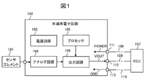
- FIG. It is a schematic block diagram of the sensor system in Example 1.
- FIG. It is a schematic block diagram of a conventional output circuit. It is an operation waveform diagram at the time of operation of a conventional output circuit, and at the time of disconnection of a power supply line.
- FIG. It is an operation waveform figure at the time of the operation of the output circuit in Example 1 and at the time of disconnection of a power supply line.
- FIG. It is a schematic block diagram of the electronic circuit in Example 4.
- FIG. It is a schematic block diagram of the electronic circuit in Example 5.
- circuit elements constituting each functional block of the embodiment are not particularly limited, but are formed on a semiconductor substrate such as single crystal silicon by an integrated circuit technique such as a known CMOS (complementary MOS) transistor.
- CMOS complementary MOS
- FIG. 1 is a schematic configuration diagram of the sensor system in this embodiment.
- the sensor system shown in FIG. 1 is, for example, an in-vehicle sensor system, which includes a sensor element 101, a semiconductor electronic circuit 102, and an ECU 107.
- the sensor element 101 is an element whose electrical characteristics change according to a physical quantity, and outputs an electric signal according to a change in a detection target.
- the sensor element 101 is, for example, an air flow sensor or the like which is an element for measuring the amount of air taken in by the engine, but is not particularly limited thereto. That is, the sensor element 101 converts physical quantities such as air flow rate, temperature, humidity, and pressure into electric signals and outputs them.
- the semiconductor electronic circuit 102 includes a power supply circuit 103, an analog circuit 104, a processor 105, and an output circuit 106, and is composed of, for example, one semiconductor chip.
- the semiconductor electronic circuit 102 mainly processes an electric signal from the sensor element 101, and outputs the processed result as a SENT (Single Edge Nibble Transmission) signal, a frequency modulation output signal, or the like via the output circuit 106. In some cases, the circuit outputs as a nalog signal voltage.
- the analog circuit 104 performs processing such as amplification, filtering, analog / digital conversion, and digital / analog conversion on the electric signal from the sensor element 101.
- the processor 105 processes digital data, controls peripheral circuits, and the like.
- the power supply circuit 103 generates an internal power supply from an external power supply and distributes it to each circuit.
- the output circuit 106 receives the processing result from the analog circuit 104 or the processor 105, and outputs an output signal (for example, a SENT signal) VOUT to the ECU 107 via the output terminal 112 and the output wiring 109. Further, the power supply POWER is given from the ECU 107 or other external device via the power supply line 108 and the power supply terminal 111, and is connected to the ground GND via the ground terminal 113.
- Reference numeral 110 is ground wiring.
- FIG. 2 is an example of a conventional output circuit.
- the output circuit 201 includes a control circuit 202, loads 203 and 204, a power supply terminal 111, and an output terminal 112.
- a power supply line 108 is connected to the power supply terminal 111, and power is supplied from the outside such as an ECU. Further, an output line is connected to the output terminal 206 to transmit an output signal to an external controller such as an ECU.
- This output line is connected to a predetermined voltage in the interface circuit of the ECU via a pull-up resistor 120.
- the predetermined pull-up resistor 120 is, for example, 1 k ⁇ to several tens of k ⁇ .
- the load 203 and 204 are controlled by the control circuit 202 in order to output data reflecting a sensor signal or the like.
- FIG. 3 shows a voltage waveform when the power supply line is disconnected from the operating state.
- the upper waveform shows the voltage of the power supply terminal
- the lower waveform shows the voltage of the output terminal
- the output line 108 is disconnected, power will not be supplied to the output circuit 201.
- the output line is connected to a predetermined voltage on the ECU side via the pull-up resistor 120, a current flows from the output terminal to the power supply line in the output circuit via the load as shown in FIG. ..
- the load is a MOSFET, a current may flow through a parasitic diode between the drain and the back gate.
- the output resistance of the output terminal is designed to be about several tens of ⁇ to 1 k ⁇ in order to drive the output line and enhance noise immunity. Therefore, since the resistance is lower than that of the pull-up resistor, the output terminal voltage does not become a predetermined voltage that is pulled up, but becomes an intermediate potential (304).
- the electronic circuit for the sensor needs a diagnostic function at the time of failure.
- the power supply line is broken and the sensor electronic circuit is not supplied with power, it is necessary to recognize that the power supply line is broken by the external circuit. More specifically, by fixing the output signal as a high level to a potential different from the usual one, it is possible to recognize the disconnection state.
- the output terminal voltage is a predetermined voltage in order to recognize that the wire is broken.
- the output resistance of the output circuit is required to be high, and the pull-up voltage is required to be substantially equal to the voltage to which the pull-up resistor is connected.
- FIG. 4 is a schematic configuration diagram of an electronic circuit equipped with an output circuit in this embodiment.
- the electronic circuit 400 is composed of a load 401, a transistor 402, a current generation circuit 403, a current-voltage conversion circuit 404, a power supply terminal 111, and an output terminal 112.
- the current-voltage conversion circuit 404 is composed of a current mirror circuit composed of MIMO FETs 407 and 408, a resistor 409, an NMOS FET 410, and a NMOS FET 411.
- the current generation circuit 403 uses the power from the power supply terminal 111 to generate a reference current IREF.
- the reference current is mirrored by the current mirror circuit and the resistor 409 converts the current into a voltage.
- the control signal VCTL during operation becomes a high level. Since this voltage is inverted by the NMOS FET 410, the transistor 402 is turned on in order to control the gate voltage of the transistor 402 with a low level signal. Further, the PRIVATE FET 411 is turned off because the gate voltage becomes high level. Therefore, during normal operation, the transistor 402 is controlled to be turned on, the output line is driven by the load 401, and a signal is output from the output terminal 112.
- the operation when the power supply line is broken will be described.
- the electronic circuit continues to operate for a certain period of time due to the electric charge accumulated in the capacity of the electronic circuit side of the power supply line disconnection portion. Then, in the electronic circuit, the electric charge is consumed by the circuit, so that the power supply voltage drops, and the circuit becomes inoperable as the power supply voltage drops.
- the output circuit consumes a large amount of current when the circuit stops operating. Specifically, the circuit operation stops near the voltage at which the power supply voltage in the electronic circuit drops to the vicinity of the threshold voltage corresponding to the number of stages in which the transistors are vertically stacked. As the current consumption decreases, the voltage itself is less likely to drop further.
- the current value of the reference current IREF which is the output of the current generation circuit 403, decreases and approaches zero.
- the output current of the current mirror circuit also decreases, the voltage drop at the resistor 409 becomes small, and the control signal VCTL becomes low level.
- the gate potential of the NMOS FET 410 becomes low level, it is turned off.
- the epitaxial FET 411 is turned on, the gate voltage of the transistor 402 becomes a voltage substantially equal to the output terminal voltage.
- the transistor 402 is turned off, the impedance from the output terminal 112 to the power supply line in the electronic circuit becomes high, and the current inflow from the output terminal 112 to the power supply line in the electronic circuit can be suppressed, and therefore, the middle of the output terminal 112.
- the potential can be suppressed. Therefore, the potential of the output terminal 112 becomes a voltage substantially equal to the voltage pulled up on the ECU 107 side, and it can be recognized that the power supply line is disconnected. That is, the PRIVATE FET 411 is a switch for connecting the gate terminal of the transistor 402 and the wiring to which the output terminal is connected at the time of disconnection.
- FIG. 5 is an operation waveform diagram of the electronic circuit in this embodiment during operation and when the power supply line is broken.
- the same functions as those in FIG. 3 are designated by the same reference numerals, and the description thereof will be omitted.
- the upper waveform shows the voltage of the power supply terminal
- the middle waveform shows the current IREF in FIG. 4
- the lower waveform shows the voltage of the output terminal.
- a power supply voltage is given and an output signal is output.
- the reference current IREF (503) is generated, and the control voltage VCTL becomes high level.
- the control voltage VCTL becomes low level
- the transistor 402 is turned off, and the output terminal voltage becomes a high level voltage substantially equal to the pull-up voltage.
- a current is generated using the voltage connected to the power supply line in the electronic circuit, and the transistor is controlled using the voltage that changes with the current, so that the intermediate potential of the output terminal when the power supply line is disconnected Can be suppressed, the output impedance can be increased, and a high level output can be obtained. Further, by using the current, the output terminal can be set to a high level even when the power supply terminal voltage does not drop below a certain level due to disconnection of the power supply line during operation.
- the electronic circuit in this embodiment can bring the voltage to the ground level even when the power supply is cut off by generating the control voltage VCTL using the pull-down resistor.
- the load has been described as a transistor in this embodiment, the load is not limited to this, and may be, for example, a resistor.
- the output resistance can be set to a substantially constant resistance value without depending on the output voltage. Further, the positional relationship between the load and the transistor is not limited to this.
- the power supply voltage is 5V.
- the reference current IREF, the mirroring current, and the pull-down resistor are set as follows. For example, assume that 10 ⁇ A is used as the reference current IREF.
- the mirror ratio may be 1: 1 or may be, for example, 1: 4 with a gain of 4 times.
- the voltage is 12 V if a current of 40 uA flows through the pull-down resistor.
- the control voltage is a value of about 5 V, which is close to the power supply voltage. That is, during normal operation, the control voltage is 5 V, which is substantially equal to the power supply voltage.
- the power supply terminal voltage drops and the mirror current decreases.
- the threshold voltage of the NMOS FET is 0.9V, when the current decreases to about 3 ⁇ A, the threshold voltage of the NMOS FET is lowered and the NMOS FET is turned off.
- the control voltage can be set to a high level during normal operation, and the transistor can be turned on reliably. Can be done.
- the current generation circuit 403 uses a circuit that outputs as a current, such as by using a bandgap reference circuit. Further, instead of directly using the voltage given to the power supply terminal, a circuit that generates a current by using the voltage obtained by voltage conversion using a regulator as a power source may be used.
- a control voltage may be generated by a current-voltage conversion circuit using an operational amplifier and a resistor.
- the on / off of the transistor is controlled by using the control voltage that changes according to the change of the current generated by using the power supply terminal voltage, it is appropriate when the power supply line is broken. Therefore, it is possible to output a high-level potential when a disconnection occurs, and it is possible to provide a circuit in which the accuracy of disconnection detection is improved.
- FIG. 6 is a schematic configuration diagram of an electronic circuit equipped with an output circuit in this embodiment.
- the electronic circuit 600 is composed of a load 401, a transistor 402, a current generation circuit 403, a current-voltage conversion circuit 404, a power supply terminal 111, an output terminal 112, and a board control circuit 604.
- the board control circuit 604 is composed of MIMO FETs 601 and 602. When the transistor 402 is composed of a MIMO FET, a parasitic diode exists between the drain terminal and the back gate terminal and between the source terminal and the back gate terminal.
- the back gate terminal of the transistor 402 is controlled so as to be connected to the power supply voltage during operation and to the output voltage of the output terminal when the power supply line is broken. Since the control voltage VCTLB is at a low level during operation, the polyclonal FET 601 is turned on, the back gate terminal of the transistor 402 is connected to the power supply voltage, and the power supply voltage is maintained. Further, when the power supply line is disconnected, the output terminal voltage becomes higher than the power supply voltage. Therefore, the MIMO FET 601 is turned off, the MIMO FET 602 is turned on, and the back gate terminal voltage of the transistor 402 is connected to the output terminal voltage.
- the current of the current generation circuit 403 that generates a current by using the power from the power supply line in the electronic circuit is used, and the voltage obtained by the current-voltage conversion by the current-voltage conversion circuit 404 is used. Take control. In this way, by controlling the back gate terminal voltage of the transistor 402 and controlling the gate voltage by using the voltage passing through the current generation circuit 403 and the current-voltage conversion circuit 404, the electrons of the output terminal are electronic when the power supply line is disconnected. The circuit can be put into a high impedance state and controlled to output a high level.
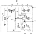
- FIG. 7 is a schematic configuration diagram of an electronic circuit equipped with an output circuit in this embodiment.
- the electronic circuit 700 includes loads 703 and 706, transistors 402, current generation circuit 403, current-voltage conversion circuit 404, power supply terminal 111, and output terminal 112.
- the loads 703 and 706 are current mirror circuits whose outputs are driven by a constant current.
- the current mirror circuit for output is composed of NMOS FETs 704 and 705 as a load 706 on the sink side and MPLS FETs 701 and 702 as a load 703 on the source side.
- the output load By outputting a constant current, the output load can be driven appropriately. For example, it is driven by a current of about several mA to 10 mA. Assuming that the amplitude of the output signal is 5 V and the output current is 5 mA, the output resistance is 1 k ⁇ when the potential difference is 5 V. Further, for example, when the potential difference is 1 V, the output resistance is 200 ⁇ . The value of this output resistor is smaller than that of the pull-up resistor. Therefore, when the power supply line is broken, it is necessary to turn off the transistor 402 or turn it into a high impedance state.
- the transistor 402 By generating a current with the current generation circuit 403, performing current-voltage conversion with the current-voltage conversion circuit 404, and controlling the gate voltage of the transistor 402, the transistor 402 is controlled on during operation to achieve a low output impedance state. When the power supply line is broken, the transistor 402 is controlled to be turned off to obtain a high output impedance state. In this way, when the power supply line is broken, the current inflow to the output terminal is suppressed, and high level output becomes possible.
- FIG. 8 is a schematic configuration diagram of an electronic circuit equipped with an output circuit in this embodiment.
- the same functions as those in FIG. 4 are designated by the same reference numerals, and the description thereof will be omitted.
- the difference from FIG. 4 is that the load 801 is a resistor.
- the load may be a passive element such as a resistor instead of an active element such as a transistor.
- the configuration may be such that a transistor and a resistor are combined.
- FIG. 9 is a schematic configuration diagram of an electronic circuit equipped with an output circuit in this embodiment.
- the same functions as those in FIG. 7 are designated by the same reference numerals, and the description thereof will be omitted.
- the difference from FIG. 7 is that the current-voltage conversion circuit 910 is composed of a cascode-connected current mirror circuit 905.
- the current mirror circuit 905 is composed of MIMO FETs 901, 902, 903, and 904.
- the MIMO FET tends to operate in the unsaturated region, the mirrored current decreases at an early stage, and the potential of the control voltage VCTL drops due to the pull-down resistor.
- the gate voltage of the transistor 402 is controlled by the control voltage VCTLB and turned off.
- the current mirror circuit By connecting the current mirror circuit with cascode in this way, the number of vertically stacked stages increases, and when the power supply terminal voltage drops when the power supply line is disconnected, the current can be reliably cut off and high-level output can be achieved. .. By cutting off the current earlier than the current supply capacity of the current generation circuit 403 by the current mirror circuit, it is possible to prevent the current generation circuit from operating due to the current wrapping around the power supply line in the electronic circuit from the output terminal. it can.
- FIG. 10 is a schematic configuration diagram of an electronic circuit equipped with an output circuit in this embodiment.
- the electronic circuit 1000 includes loads 703 and 706, transistors 402, and control voltage generation circuit 1001. Even if the power supply terminal voltage does not drop when the power supply line is disconnected, the potential of the control voltage VCTL is reduced to a voltage lower than the threshold voltage of the NMOS FET 410 by dropping the potential with the diode-connected MOSFET FET 1002 and using it for control. can do. Therefore, even if the power supply terminal voltage does not drop when the power supply line is disconnected, the gate voltage of the transistor 402 can be controlled, and the transistor 402 can be turned off to suppress the intermediate potential of the output terminal voltage.
- this element is not limited to the epitaxial FET, and a constant voltage diode or the like may be used.
- control may be performed using a resistor and a voltage obtained by dividing the power supply voltage.
- the present invention is not limited to the above-mentioned examples, and includes various modifications.
- the above-described embodiment has been described in detail in order to explain the present invention in an easy-to-understand manner, and is not necessarily limited to those having all the described configurations.
- it is possible to replace a part of the configuration of one embodiment with the configuration of another embodiment and it is also possible to add the configuration of another embodiment to the configuration of one embodiment.
- 101 Sensor element
- 102 Semiconductor electronic circuit
- 103 Power supply circuit
- 104 Analog circuit
- 105 Processor
- 106 Processor
- 201 Output circuit
- 400 600, 700, 800, 900, 1000: Electronic circuit
- 108 Power supply line
- 109 Output wiring
- 110 Ground wiring
- 111 Power supply terminal
- 112 Output terminal
- 113 Ground terminal
- 202 Control circuit
- 402 Transistor
- 403 Current generation circuit
- 404, 910 Current-voltage conversion circuit
Landscapes
- Physics & Mathematics (AREA)
- General Physics & Mathematics (AREA)
- Electromagnetism (AREA)
- Engineering & Computer Science (AREA)
- General Engineering & Computer Science (AREA)
- Logic Circuits (AREA)
- Testing Of Short-Circuits, Discontinuities, Leakage, Or Incorrect Line Connections (AREA)
- Electronic Switches (AREA)
- Semiconductor Integrated Circuits (AREA)
Priority Applications (3)
| Application Number | Priority Date | Filing Date | Title |
|---|---|---|---|
| CN202080034215.9A CN113796009B (zh) | 2019-05-31 | 2020-04-03 | 电子电路和传感器系统 |
| US17/595,051 US12047062B2 (en) | 2019-05-31 | 2020-04-03 | Electronic circuit and sensor system |
| DE112020002140.8T DE112020002140T5 (de) | 2019-05-31 | 2020-04-03 | Elektronische schaltung und sensorsystem |
Applications Claiming Priority (2)
| Application Number | Priority Date | Filing Date | Title |
|---|---|---|---|
| JP2019102665A JP7403238B2 (ja) | 2019-05-31 | 2019-05-31 | 電子回路およびセンサシステム |
| JP2019-102665 | 2019-05-31 |
Publications (1)
| Publication Number | Publication Date |
|---|---|
| WO2020241046A1 true WO2020241046A1 (ja) | 2020-12-03 |
Family
ID=73553393
Family Applications (1)
| Application Number | Title | Priority Date | Filing Date |
|---|---|---|---|
| PCT/JP2020/015264 Ceased WO2020241046A1 (ja) | 2019-05-31 | 2020-04-03 | 電子回路およびセンサシステム |
Country Status (5)
| Country | Link |
|---|---|
| US (1) | US12047062B2 (https=) |
| JP (1) | JP7403238B2 (https=) |
| CN (1) | CN113796009B (https=) |
| DE (1) | DE112020002140T5 (https=) |
| WO (1) | WO2020241046A1 (https=) |
Cited By (1)
| Publication number | Priority date | Publication date | Assignee | Title |
|---|---|---|---|---|
| WO2022230018A1 (ja) * | 2021-04-26 | 2022-11-03 | 三菱電機株式会社 | 半導体装置 |
Families Citing this family (2)
| Publication number | Priority date | Publication date | Assignee | Title |
|---|---|---|---|---|
| JP7162755B2 (ja) * | 2019-11-14 | 2022-10-28 | 三菱電機株式会社 | 半導体装置 |
| CN117526231B (zh) * | 2024-01-08 | 2024-03-26 | 赛卓电子科技(上海)股份有限公司 | 一种断线保护电路及传感器 |
Citations (6)
| Publication number | Priority date | Publication date | Assignee | Title |
|---|---|---|---|---|
| JP2005252968A (ja) * | 2004-03-08 | 2005-09-15 | Denso Corp | 過電流保護回路 |
| JP2007295209A (ja) * | 2006-04-25 | 2007-11-08 | Renesas Technology Corp | アナログスイッチ回路 |
| JP2008029067A (ja) * | 2006-07-19 | 2008-02-07 | Elm Technology Corp | 2次電池用保護回路を有するバッテリーパック |
| JP2016070835A (ja) * | 2014-09-30 | 2016-05-09 | パナソニックIpマネジメント株式会社 | 検出装置及び検出システム |
| WO2017179158A1 (ja) * | 2016-04-13 | 2017-10-19 | 株式会社 東芝 | 電池モジュール |
| JP2017191093A (ja) * | 2016-04-06 | 2017-10-19 | 株式会社デンソー | 回転検出装置、および、これを用いた電動パワーステアリング装置 |
Family Cites Families (15)
| Publication number | Priority date | Publication date | Assignee | Title |
|---|---|---|---|---|
| JP3287624B2 (ja) | 1993-01-11 | 2002-06-04 | 三菱電機株式会社 | 半導体センサ |
| JPH08146069A (ja) * | 1994-11-18 | 1996-06-07 | Nissan Motor Co Ltd | 断線自動検知装置 |
| JP3382528B2 (ja) * | 1998-01-23 | 2003-03-04 | キヤノン株式会社 | カレントミラー回路 |
| JP4089125B2 (ja) * | 2000-04-12 | 2008-05-28 | 株式会社デンソー | 電気負荷駆動装置 |
| JP4300773B2 (ja) * | 2002-08-22 | 2009-07-22 | トヨタ自動車株式会社 | 異常検出装置 |
| JP4296811B2 (ja) * | 2003-03-25 | 2009-07-15 | 株式会社デンソー | 物理量センサ装置 |
| JP4082261B2 (ja) | 2003-03-31 | 2008-04-30 | 株式会社デンソー | センサ装置用断線検出回路 |
| JP4398312B2 (ja) * | 2004-07-06 | 2010-01-13 | 矢崎総業株式会社 | 半導体スイッチの制御装置 |
| JP4665725B2 (ja) * | 2005-11-14 | 2011-04-06 | 株式会社デンソー | 物理量検出装置 |
| JP2010216996A (ja) * | 2009-03-17 | 2010-09-30 | Ricoh Co Ltd | 半導体装置および該半導体装置の検査方法 |
| JP2011089849A (ja) * | 2009-10-21 | 2011-05-06 | Asahi Kasei Electronics Co Ltd | 断線検出装置 |
| JP2013016959A (ja) * | 2011-07-01 | 2013-01-24 | Sanken Electric Co Ltd | 負荷駆動回路 |
| JP5768016B2 (ja) * | 2012-07-25 | 2015-08-26 | 日立オートモティブシステムズ株式会社 | センサ装置 |
| JP6405998B2 (ja) | 2014-12-25 | 2018-10-17 | サンケン電気株式会社 | 負荷駆動回路 |
| WO2017169057A1 (ja) * | 2016-03-31 | 2017-10-05 | 日立オートモティブシステムズ株式会社 | センサ装置 |
-
2019
- 2019-05-31 JP JP2019102665A patent/JP7403238B2/ja active Active
-
2020
- 2020-04-03 DE DE112020002140.8T patent/DE112020002140T5/de active Pending
- 2020-04-03 US US17/595,051 patent/US12047062B2/en active Active
- 2020-04-03 WO PCT/JP2020/015264 patent/WO2020241046A1/ja not_active Ceased
- 2020-04-03 CN CN202080034215.9A patent/CN113796009B/zh active Active
Patent Citations (6)
| Publication number | Priority date | Publication date | Assignee | Title |
|---|---|---|---|---|
| JP2005252968A (ja) * | 2004-03-08 | 2005-09-15 | Denso Corp | 過電流保護回路 |
| JP2007295209A (ja) * | 2006-04-25 | 2007-11-08 | Renesas Technology Corp | アナログスイッチ回路 |
| JP2008029067A (ja) * | 2006-07-19 | 2008-02-07 | Elm Technology Corp | 2次電池用保護回路を有するバッテリーパック |
| JP2016070835A (ja) * | 2014-09-30 | 2016-05-09 | パナソニックIpマネジメント株式会社 | 検出装置及び検出システム |
| JP2017191093A (ja) * | 2016-04-06 | 2017-10-19 | 株式会社デンソー | 回転検出装置、および、これを用いた電動パワーステアリング装置 |
| WO2017179158A1 (ja) * | 2016-04-13 | 2017-10-19 | 株式会社 東芝 | 電池モジュール |
Cited By (2)
| Publication number | Priority date | Publication date | Assignee | Title |
|---|---|---|---|---|
| WO2022230018A1 (ja) * | 2021-04-26 | 2022-11-03 | 三菱電機株式会社 | 半導体装置 |
| JP7657294B2 (ja) | 2021-04-26 | 2025-04-04 | 三菱電機株式会社 | 半導体装置 |
Also Published As
| Publication number | Publication date |
|---|---|
| JP2020198499A (ja) | 2020-12-10 |
| JP7403238B2 (ja) | 2023-12-22 |
| CN113796009B (zh) | 2024-12-20 |
| DE112020002140T5 (de) | 2022-01-13 |
| US12047062B2 (en) | 2024-07-23 |
| US20220216867A1 (en) | 2022-07-07 |
| CN113796009A (zh) | 2021-12-14 |
Similar Documents
| Publication | Publication Date | Title |
|---|---|---|
| US7116129B2 (en) | Temperature-compensated output buffer method and circuit | |
| CN210129850U (zh) | 输出缓冲电路 | |
| US9551735B2 (en) | Sensor device with series circuit of MOS switch and capacitor | |
| KR20010049227A (ko) | 레벨조정회로 및 이를 포함하는 데이터 출력회로 | |
| WO2020241046A1 (ja) | 電子回路およびセンサシステム | |
| US6384682B2 (en) | Differential amplifier circuit and pull up-type differential driver | |
| US6414521B1 (en) | Sense amplifier systems and methods | |
| US6621329B2 (en) | Semiconductor device | |
| US5864254A (en) | Differential amplifier circuit with enlarged range for source voltage and semiconductor device using same | |
| JP7162755B2 (ja) | 半導体装置 | |
| US12525939B2 (en) | Semiconductor integrated circuit device | |
| US7336122B2 (en) | Low power high side current monitor which operates at high voltages and method therefor | |
| US7965125B2 (en) | Current drive circuit | |
| US7724486B2 (en) | Sensing a current signal in an integrated circuit | |
| JP6332601B2 (ja) | 半導体集積回路装置 | |
| US20070146023A1 (en) | Reset signal generating circuit and semiconductor integrated circuit device | |
| CN103650338A (zh) | 前馈有源解耦 | |
| US20240291485A1 (en) | Power switch with soft diode connection | |
| JP6970644B2 (ja) | 半導体装置およびセンサシステム | |
| KR102495033B1 (ko) | 전자 소자 및 이를 포함하는 시스템 | |
| KR100902121B1 (ko) | 내부전원 생성장치 | |
| TW202414784A (zh) | 化合物半導體積體電路以及系統 | |
| JPH06334124A (ja) | 半導体集積回路 | |
| WO2022107416A1 (ja) | 電子装置 | |
| CN112311337A (zh) | 半导体装置 |
Legal Events
| Date | Code | Title | Description |
|---|---|---|---|
| 121 | Ep: the epo has been informed by wipo that ep was designated in this application |
Ref document number: 20814076 Country of ref document: EP Kind code of ref document: A1 |
|
| 122 | Ep: pct application non-entry in european phase |
Ref document number: 20814076 Country of ref document: EP Kind code of ref document: A1 |