WO2020234681A1 - 半導体装置、及び電子機器 - Google Patents
半導体装置、及び電子機器 Download PDFInfo
- Publication number
- WO2020234681A1 WO2020234681A1 PCT/IB2020/054307 IB2020054307W WO2020234681A1 WO 2020234681 A1 WO2020234681 A1 WO 2020234681A1 IB 2020054307 W IB2020054307 W IB 2020054307W WO 2020234681 A1 WO2020234681 A1 WO 2020234681A1
- Authority
- WO
- WIPO (PCT)
- Prior art keywords
- circuit
- wiring
- switch
- terminal
- potential
- Prior art date
- Legal status (The legal status is an assumption and is not a legal conclusion. Google has not performed a legal analysis and makes no representation as to the accuracy of the status listed.)
- Ceased
Links
Images








































Classifications
-
- G—PHYSICS
- G06—COMPUTING OR CALCULATING; COUNTING
- G06N—COMPUTING ARRANGEMENTS BASED ON SPECIFIC COMPUTATIONAL MODELS
- G06N3/00—Computing arrangements based on biological models
- G06N3/02—Neural networks
- G06N3/06—Physical realisation, i.e. hardware implementation of neural networks, neurons or parts of neurons
- G06N3/063—Physical realisation, i.e. hardware implementation of neural networks, neurons or parts of neurons using electronic means
-
- G—PHYSICS
- G06—COMPUTING OR CALCULATING; COUNTING
- G06G—ANALOGUE COMPUTERS
- G06G7/00—Devices in which the computing operation is performed by varying electric or magnetic quantities
- G06G7/12—Arrangements for performing computing operations, e.g. operational amplifiers specially adapted therefor
- G06G7/16—Arrangements for performing computing operations, e.g. operational amplifiers specially adapted therefor for multiplication or division
-
- G—PHYSICS
- G06—COMPUTING OR CALCULATING; COUNTING
- G06G—ANALOGUE COMPUTERS
- G06G7/00—Devices in which the computing operation is performed by varying electric or magnetic quantities
- G06G7/12—Arrangements for performing computing operations, e.g. operational amplifiers specially adapted therefor
- G06G7/18—Arrangements for performing computing operations, e.g. operational amplifiers specially adapted therefor for integration or differentiation; for forming integrals
- G06G7/184—Arrangements for performing computing operations, e.g. operational amplifiers specially adapted therefor for integration or differentiation; for forming integrals using capacitive elements
-
- G—PHYSICS
- G06—COMPUTING OR CALCULATING; COUNTING
- G06G—ANALOGUE COMPUTERS
- G06G7/00—Devices in which the computing operation is performed by varying electric or magnetic quantities
- G06G7/12—Arrangements for performing computing operations, e.g. operational amplifiers specially adapted therefor
- G06G7/19—Arrangements for performing computing operations, e.g. operational amplifiers specially adapted therefor for forming integrals of products, e.g. Fourier integrals, Laplace integrals or correlation integrals; for analysis or synthesis of functions using orthogonal functions
-
- G—PHYSICS
- G06—COMPUTING OR CALCULATING; COUNTING
- G06G—ANALOGUE COMPUTERS
- G06G7/00—Devices in which the computing operation is performed by varying electric or magnetic quantities
- G06G7/48—Analogue computers for specific processes, systems or devices, e.g. simulators
- G06G7/60—Analogue computers for specific processes, systems or devices, e.g. simulators for living beings, e.g. their nervous systems ; for problems in the medical field
-
- G—PHYSICS
- G11—INFORMATION STORAGE
- G11C—STATIC STORES
- G11C11/00—Digital stores characterised by the use of particular electric or magnetic storage elements; Storage elements therefor
- G11C11/54—Digital stores characterised by the use of particular electric or magnetic storage elements; Storage elements therefor using elements simulating biological cells, e.g. neuron
-
- H—ELECTRICITY
- H10—SEMICONDUCTOR DEVICES; ELECTRIC SOLID-STATE DEVICES NOT OTHERWISE PROVIDED FOR
- H10B—ELECTRONIC MEMORY DEVICES
- H10B12/00—Dynamic random access memory [DRAM] devices
- H10B12/01—Manufacture or treatment
- H10B12/09—Manufacture or treatment with simultaneous manufacture of the peripheral circuit region and memory cells
-
- H—ELECTRICITY
- H10—SEMICONDUCTOR DEVICES; ELECTRIC SOLID-STATE DEVICES NOT OTHERWISE PROVIDED FOR
- H10D—INORGANIC ELECTRIC SEMICONDUCTOR DEVICES
- H10D30/00—Field-effect transistors [FET]
- H10D30/60—Insulated-gate field-effect transistors [IGFET]
- H10D30/67—Thin-film transistors [TFT]
- H10D30/674—Thin-film transistors [TFT] characterised by the active materials
- H10D30/6755—Oxide semiconductors, e.g. zinc oxide, copper aluminium oxide or cadmium stannate
-
- H—ELECTRICITY
- H10—SEMICONDUCTOR DEVICES; ELECTRIC SOLID-STATE DEVICES NOT OTHERWISE PROVIDED FOR
- H10B—ELECTRONIC MEMORY DEVICES
- H10B12/00—Dynamic random access memory [DRAM] devices
- H10B12/50—Peripheral circuit region structures
-
- H—ELECTRICITY
- H10—SEMICONDUCTOR DEVICES; ELECTRIC SOLID-STATE DEVICES NOT OTHERWISE PROVIDED FOR
- H10D—INORGANIC ELECTRIC SEMICONDUCTOR DEVICES
- H10D87/00—Integrated devices comprising both bulk components and either SOI or SOS components on the same substrate
Definitions
- One aspect of the present invention relates to a semiconductor device and an electronic device.
- one aspect of the present invention is not limited to the above technical fields.
- the technical field of the invention disclosed in the present specification and the like relates to a product, a method, or a manufacturing method.
- one aspect of the invention relates to a process, machine, manufacture, or composition (composition of matter). Therefore, more specifically, the technical fields of one aspect of the present invention disclosed in the present specification include semiconductor devices, display devices, liquid crystal display devices, light emitting devices, power storage devices, image pickup devices, storage devices, signal processing devices, and processors.
- Electronic devices, systems, their driving methods, their manufacturing methods, or their inspection methods can be mentioned as examples.
- the mechanism of the brain is incorporated as an electronic circuit, and has a circuit corresponding to "neurons” and "synapses" of the human brain. Therefore, such integrated circuits are sometimes called “neuromorphic", “brainmorphic”, or “braininspire”.
- the integrated circuit has a non-Von Neumann architecture, and is expected to be able to perform parallel processing with extremely low power consumption as compared with the von Neumann architecture in which the power consumption increases as the processing speed increases.
- Non-Patent Document 1 and Non-Patent Document 2 disclose an arithmetic unit that constitutes an artificial neural network using SRAM (Static Random Access Memory).
- a calculation is performed by multiplying the synaptic connection strength (sometimes called a weighting coefficient) that connects two neurons with the signal transmitted between the two neurons.
- the connection strength of each synapse between the plurality of first neurons in the first layer and one of the second neurons in the second layer and the plurality of first neurons in the first layer It is necessary to multiply and add (perform a product-sum operation) with each signal input to one of the second neurons of the second layer from, and depending on the scale of the artificial neural network, for example, the connection strength.
- the number and the number of parameters indicating the signal are determined. That is, in an artificial neural network, as the number of layers, the number of neurons, etc. increases, the number of circuits corresponding to each of "neurons" and "synapses" increases, and the amount of calculation may become enormous.
- the operation of the neural network includes the operation of the activation function in addition to the product-sum operation.
- the larger the scale of the artificial neural network the higher the power consumption tends to be.
- One aspect of the present invention is to provide a semiconductor device or the like in which a hierarchical artificial neural network is constructed. Alternatively, one aspect of the present invention is to provide a semiconductor device or the like having low power consumption. Alternatively, one aspect of the present invention is to provide a new semiconductor device or the like. Alternatively, one aspect of the present invention is to provide an electronic device having the above semiconductor device.
- the problem of one aspect of the present invention is not limited to the problems listed above.
- the issues listed above do not preclude the existence of other issues.
- Other issues are issues not mentioned in this item, which are described below. Issues not mentioned in this item can be derived from descriptions in the description, drawings, etc. by those skilled in the art, and can be appropriately extracted from these descriptions.
- one aspect of the present invention solves at least one of the above-listed problems and other problems. It should be noted that one aspect of the present invention does not need to solve all of the above-listed problems and other problems.
- One aspect of the present invention includes a cell, a first circuit, the first circuit has a first capacitance, a first input terminal, and a second input terminal, and the cell is the first.
- the cell is electrically connected to the first input terminal via the wiring, the cell is electrically connected to the second input terminal via the second wiring, and the cell has a function of holding the first data and the cell.
- the first capacitance is a difference voltage between a first potential corresponding to the first current and a second potential corresponding to the second current. It is a semiconductor device having a function of holding the above.
- the first circuit has a second circuit, and the second circuit acquires a difference voltage and outputs a signal corresponding to the difference voltage. It is a semiconductor device having a function.
- the first circuit includes a first current-voltage conversion circuit, a second current-voltage conversion circuit, a first switch, a second switch, and a third. It has a switch and a fourth switch, and the first input terminal is electrically connected to the first terminal of the first switch and the first terminal of the first current-voltage conversion circuit, and is of the first switch.
- the second terminal is electrically connected to the first terminal of the second switch and the first terminal of the first capacitance, and the second input terminal is the first terminal of the third switch and the second current-voltage conversion.
- the second terminal of the third switch is electrically connected to the first terminal of the fourth switch and the second terminal of the first capacitance, and is the fourth.
- the second terminal of the switch is electrically connected to the first terminal of the second circuit, and the first current-voltage conversion circuit responds to the first current input to the first terminal of the first current-voltage conversion circuit. It has a function to set the potential of the first terminal of the first current-voltage conversion circuit to the first potential, and the second current-voltage conversion circuit responds to the second current input to the first terminal of the second current-voltage conversion circuit. Therefore, it is a semiconductor device having a function of setting the potential of the first terminal of the second current-voltage conversion circuit to the second potential.
- the second terminal of the second switch is electrically connected to the third wiring that gives a reference potential, and the first circuit is connected to the first switch.
- the third switch is turned on, the second switch and the fourth switch are turned off, the first terminal of the first capacitance is set to the first potential, and the second terminal of the first capacitance is set to the second potential.
- the function to switch, the first switch, the third switch, and the fourth switch are turned off, the second switch is turned on, and the first terminal of the first capacitance is changed from the first potential to the reference potential.
- the function of changing the second potential of the second terminal of the first capacitance to the third potential by the capacitance coupling, the first switch, the second switch, and the third switch are turned off, and the second 4
- This is a semiconductor device having a function of turning on a switch and inputting a third potential corresponding to a differential voltage to the first terminal of the second circuit.
- one aspect of the present invention includes a cell, a first circuit, and the first circuit has a first capacitance, a second capacitance, a first input terminal, and a second input terminal. Then, the cell is electrically connected to the first input terminal via the first wiring, the cell is electrically connected to the second input terminal via the second wiring, and the cell is the first data. By the function of holding the cell and the second data being input to the cell, a first current corresponding to the first data and the second data is passed between the cell and the first wiring, and the cell and the second wiring.
- the first capacitance has a function of passing a second current according to the first data and the second data between the two, and the first capacitance has a first potential corresponding to the first current and a second current corresponding to the second current. It has a function of holding the first differential voltage of the two potentials, and the second capacitance holds the second differential voltage of the first potential corresponding to the first current and the second potential corresponding to the second current. It is a semiconductor device having a holding function.
- the first circuit has a second circuit and a third circuit
- the second circuit is the potential of the first terminal of the first capacitance.
- the third circuit is based on the potential of the second terminal of the second capacitance.
- a semiconductor device having a function of acquiring a second differential voltage and outputting a second signal corresponding to the second differential voltage.
- the first circuit includes a first current-voltage conversion circuit, a second current-voltage conversion circuit, a first switch, a second switch, and a third. It has a switch, a fourth switch, a fifth switch, a sixth switch, a seventh switch, and an eighth switch, and the first input terminal is the first terminal and the fifth switch of the first switch.
- the first terminal of the first switch and the first terminal of the first current-voltage conversion circuit are electrically connected, and the second terminal of the first switch is the first terminal of the second switch and the first terminal of the first capacitance.
- the second terminal of the fifth switch is electrically connected to the first terminal of the sixth switch and the first terminal of the second capacitance
- the second input terminal is the second. It is electrically connected to the first terminal of the third switch, the first terminal of the seventh switch, and the first terminal of the second current-voltage conversion circuit, and the second terminal of the third switch is the fourth terminal of the fourth switch. It is electrically connected to the 1st terminal and the 2nd terminal of the 1st capacity, and the 2nd terminal of the 7th switch is electrically connected to the 1st terminal of the 8th switch and the 2nd terminal of the 2nd capacity.
- the second terminal of the fourth switch is electrically connected to the first terminal of the second circuit
- the second terminal of the sixth switch is electrically connected to the first terminal of the third circuit.
- the current-voltage conversion circuit has a function of setting the potential of the first terminal of the first current-voltage conversion circuit to the first potential according to the first current input to the first terminal of the first current-voltage conversion circuit.
- the second current-voltage conversion circuit has a function of setting the potential of the first terminal of the second current-voltage conversion circuit to the second potential according to the second current input to the first terminal of the second current-voltage conversion circuit.
- the second terminal of the second switch is electrically connected to the third wiring that gives the reference potential
- the second terminal of the eighth switch is the reference. It is electrically connected to the third wiring that gives an electric potential
- the first circuit turns on the first switch and the third switch, turns off the second switch and the fourth switch, and sets the second switch. The function of setting the first terminal of the first capacitance to the first potential and the second terminal of the first capacitance to the second potential, turning on the fifth switch and the seventh switch, and turning on the sixth switch and the eighth switch.
- the function of turning off the switch, setting the first terminal of the second capacitance to the first potential, and setting the second terminal of the second capacitance to the second potential, the first switch, the third switch, and the fourth By turning off the switch and turning on the second switch and changing the first terminal of the first capacitance from the first potential to the reference potential, the second terminal of the first capacitance is changed by capacitance coupling.
- the function of changing the 2nd potential to the 3rd potential, the 5th switch, the 6th switch, and the 7th switch are turned off, the 8th switch is turned on, and the 2nd terminal of the 2nd capacitance is turned on.
- the cell has a first cell and a second cell, and the first cell is the first wiring.
- the second cell is electrically connected to the second wiring, the first input wiring, and the second input wiring, and the second cell is the first wiring, the second wiring, the first input wiring, and the second input. It is electrically connected to the wiring, and each of the first input wiring and the second input wiring has a function of giving a potential according to the second data, and the first cell is the first input to the first input wiring.
- the function to flow the first current to the first wiring and the second input potential are input to the first input wiring and the second input
- the function to flow the second current to the second wiring, the second input potential is input to the first input wiring, and the second input potential is input to the second input wiring.
- it has a function of making a non-conducting state between the first cell and the first wiring and between the first cell and the second wiring, and the second cell is the first input wiring.
- the first cell has a first transistor, a ninth switch, a tenth switch, an eleventh switch, a twelfth switch, and a third capacitance.
- the second cell has a second transistor, a thirteenth switch, a fourteenth switch, a fifteenth switch, a sixteenth switch, and a fourth capacitance, and has a first transistor.
- the first terminal is electrically connected to the first terminal of the ninth switch, the first terminal of the tenth switch, and the first terminal of the eleventh switch, and the gate of the first transistor has a third capacitance.
- the 2nd terminal of the 9th switch is electrically connected to the 2nd terminal of the 12th switch, and the 2nd terminal of the 10th switch.
- the control terminal of the tenth switch is electrically connected to the first input wiring
- the second terminal of the eleventh switch is electrically connected to the second wiring.
- the control terminal of the 11th switch is electrically connected to the 2nd input wiring
- the 1st terminal of the 2nd transistor is the 1st terminal of the 13th switch, the 1st terminal of the 14th switch, and the 15th switch.
- the gate of the second transistor is electrically connected to the first terminal of the fourth capacitance and the first terminal of the 16th switch, and the second of the 13th switch.
- the terminals are electrically connected to the second terminal of the 16th switch, the second terminal of the 14th switch is electrically connected to the second wiring, and the control terminal of the 14th switch is electrically connected to the first input wiring.
- the second terminal of the fifteenth switch is electrically connected to the first wiring, and the control terminal of the fifteenth switch is electrically connected to the second input wiring.
- the twelfth switch has a third transistor, the third transistor has a metal oxide in the channel forming region, and the sixteenth switch
- the fourth transistor is a semiconductor device having a fourth transistor and having a metal oxide in the channel forming region.
- one aspect of the present invention is an electronic device having a semiconductor device according to any one of (1) to (11) and a housing, and performing a neural network calculation by the semiconductor device.
- the semiconductor device is a device that utilizes semiconductor characteristics, and refers to a circuit including a semiconductor element (transistor, diode, photodiode, etc.), a device having the same circuit, and the like. It also refers to all devices that can function by utilizing semiconductor characteristics. For example, an integrated circuit, a chip having an integrated circuit, and an electronic component in which the chip is housed in a package are examples of semiconductor devices. Further, the storage device, the display device, the light emitting device, the lighting device, the electronic device, and the like are themselves semiconductor devices, and may have the semiconductor device.
- an element for example, a switch, a transistor, a capacitive element, an inductor, a resistance element, a diode, a display
- One or more devices, light emitting devices, loads, etc. can be connected between X and Y.
- the switch has a function of controlling on / off. That is, the switch is in a conductive state (on state) or a non-conducting state (off state), and has a function of controlling whether or not a current flows.
- a circuit that enables functional connection between X and Y for example, a logic circuit (inverter, NAND circuit, NOR circuit, etc.), signal conversion, etc.) Circuits (DA conversion circuit, AD conversion circuit, gamma correction circuit, etc.), potential level conversion circuit (power supply circuit (boost circuit, step-down circuit, etc.), level shifter circuit that changes the signal potential level, etc.), voltage source, current source, switching Circuits, amplifier circuits (circuits that can increase signal amplitude or current amount, operational amplifiers, differential amplifier circuits, source follower circuits, buffer circuits, etc.), signal generation circuits, storage circuits, control circuits, etc.) are X and Y. It is possible to connect one or more in between. As an example, even if another circuit is sandwiched between X and Y, if the signal output from X is transmitted to Y, it is assumed that X and Y are functionally connected. To do.
- X and Y are electrically connected, it means that X and Y are electrically connected (that is, another element between X and Y). Or when they are connected with another circuit in between) and when X and Y are directly connected (that is, they are connected without sandwiching another element or another circuit between X and Y). If there is) and.
- X and Y, the source (or the first terminal, etc.) and the drain (or the second terminal, etc.) of the transistor are electrically connected to each other, and the X, the source (or the second terminal, etc.) of the transistor. (1 terminal, etc.), the drain of the transistor (or the 2nd terminal, etc.), and Y are electrically connected in this order.
- the source of the transistor (or the first terminal, etc.) is electrically connected to X
- the drain of the transistor (or the second terminal, etc.) is electrically connected to Y
- the X, the source of the transistor (such as the second terminal).
- first terminal, etc.), the drain of the transistor (or the second terminal, etc.), and Y are electrically connected in this order.
- X is electrically connected to Y via the source (or first terminal, etc.) and drain (or second terminal, etc.) of the transistor, and X, the source (or first terminal, etc.) of the transistor.
- the terminals, etc.), the drain of the transistor (or the second terminal, etc.), and Y are provided in this connection order.
- the source (or first terminal, etc.) and drain (or second terminal, etc.) of the transistor can be separated. Separately, the technical scope can be determined. It should be noted that these expression methods are examples and are not limited to these expression methods.
- X and Y are assumed to be objects (for example, devices, elements, circuits, wirings, electrodes, terminals, conductive films, layers, etc.).
- the circuit diagram shows that the independent components are electrically connected to each other, one component has the functions of a plurality of components.
- one component has the functions of a plurality of components.
- the electrical connection in the present specification also includes the case where one conductive film has the functions of a plurality of components in combination.
- the “resistance element” can be, for example, a circuit element, wiring, or the like having a resistance value higher than 0 ⁇ . Therefore, in the present specification and the like, the “resistive element” includes a wiring having a resistance value, a transistor in which a current flows between a source and a drain, a diode, a coil, and the like. Therefore, the term “resistor element” can be paraphrased into terms such as “resistance”, “load”, and “region having a resistance value”, and conversely, “resistance", “load”, and “region having a resistance value”. Can be rephrased as a term such as “resistive element”.
- the resistance value can be, for example, preferably 1 m ⁇ or more and 10 ⁇ or less, more preferably 5 m ⁇ or more and 5 ⁇ or less, and further preferably 10 m ⁇ or more and 1 ⁇ or less. Further, for example, it may be 1 ⁇ or more and 1 ⁇ 10 9 ⁇ or less.
- the “capacitance element” means, for example, a circuit element having a capacitance value higher than 0F, a wiring region having a capacitance value, a parasitic capacitance, a transistor gate capacitance, and the like. Can be. Therefore, in the present specification and the like, the “capacitive element” is not only a circuit element containing a pair of electrodes and a dielectric contained between the electrodes, but also a parasitic element appearing between the wirings. It shall include the capacitance, the gate capacitance that appears between the gate and one of the source or drain of the transistor, and the like.
- capacitor element means “capacitive element” and “parasitic”. It can be paraphrased into terms such as “capacity” and “gate capacitance”.
- the term “pair of electrodes” in “capacity” can be paraphrased as "a pair of conductors", “a pair of conductive regions", “a pair of regions” and the like.
- the value of the capacitance can be, for example, 0.05 fF or more and 10 pF or less. Further, for example, it may be 1 pF or more and 10 ⁇ F or less.
- the transistor has three terminals called a gate, a source, and a drain.
- the gate is a control terminal that controls the conduction state of the transistor.
- the two terminals that function as sources or drains are the input and output terminals of the transistor.
- One of the two input / output terminals becomes a source and the other becomes a drain depending on the high and low potentials given to the conductive type (n-channel type, p-channel type) of the transistor and the three terminals of the transistor. Therefore, in the present specification and the like, the terms source and drain can be paraphrased.
- transistors when explaining the connection relationship of transistors, "one of the source or drain” (or the first electrode or the first terminal), “the other of the source or drain” (or the second electrode, or The notation (second terminal) is used.
- it may have a back gate in addition to the above-mentioned three terminals.
- one of the transistor gate or the back gate may be referred to as a first gate
- the other of the transistor gate or the back gate may be referred to as a second gate.
- the terms “gate” and “backgate” may be interchangeable.
- the respective gates When the transistor has three or more gates, the respective gates may be referred to as a first gate, a second gate, a third gate, and the like in the present specification and the like.
- a node can be paraphrased as a terminal, a wiring, an electrode, a conductive layer, a conductor, an impurity region, etc., depending on a circuit configuration, a device structure, and the like.
- terminals, wiring, etc. can be paraphrased as nodes.
- ground potential ground potential
- the potentials are relative, and when the reference potential changes, the potential given to the wiring, the potential applied to the circuit or the like, the potential output from the circuit or the like also changes.
- “Current” is a phenomenon of electric charge transfer (electrical conduction).
- the description that "electrical conduction of a positively charged body is occurring” means that "electrical conduction of a negatively charged body is occurring in the opposite direction.” It can be paraphrased as “I am awake.” Therefore, in the present specification and the like, “current” refers to a charge transfer phenomenon (electrical conduction) accompanying the movement of carriers, unless otherwise specified.
- the carriers referred to here include electrons, holes, anions, cations, complex ions, etc., and the carriers differ depending on the system in which the current flows (for example, semiconductor, metal, electrolyte, vacuum, etc.).
- the "current direction” in the wiring or the like shall be the direction in which the positive carrier moves, and shall be described as a positive current amount.
- the direction in which the negative carrier moves is opposite to the direction of the current, and is expressed by the amount of negative current. Therefore, in the present specification and the like, if there is no notice about the positive or negative of the current (or the direction of the current), the description such as “current flows from element A to element B” means “current flows from element B to element A”. It can be paraphrased as. Further, the description such as "a current is input to the element A” can be rephrased as "a current is output from the element A” or the like.
- the ordinal numbers “first”, “second”, and “third” are added to avoid confusion of the components. Therefore, the number of components is not limited. Moreover, the order of the components is not limited. For example, the component referred to in “first” in one of the embodiments of the present specification and the like may be the component referred to in “second” in another embodiment or in the claims. There can also be. Further, for example, the component referred to in “first” in one of the embodiments of the present specification and the like may be omitted in another embodiment or in the claims.
- the terms “above” and “below” do not limit the positional relationship of the components directly above or below and in direct contact with each other.
- the electrode B does not have to be formed in direct contact with the insulating layer A, and another configuration is formed between the insulating layer A and the electrode B. Do not exclude those that contain elements.
- membrane and layer can be interchanged with each other depending on the situation.
- the terms “insulating layer” and “insulating film” may be changed to the term "insulator”.
- Electrode may be used as part of a “wiring” and vice versa.
- the terms “electrode” and “wiring” include the case where a plurality of “electrodes” and “wiring” are integrally formed.
- a “terminal” may be used as part of a “wiring” or “electrode” and vice versa.
- the term “terminal” includes a case where a plurality of "electrodes", “wiring”, “terminals” and the like are integrally formed.
- the "electrode” can be a part of the “wiring” or the “terminal”, and for example, the “terminal” can be a part of the “wiring” or the “electrode”.
- terms such as “electrode”, “wiring”, and “terminal” may be replaced with terms such as "region” in some cases.
- terms such as “wiring”, “signal line”, and “power line” can be interchanged with each other in some cases or depending on the situation.
- the reverse is also true, and it may be possible to change terms such as “signal line” and “power line” to the term “wiring”.
- a term such as “power line” may be changed to a term such as "signal line”.
- terms such as “signal line” may be changed to terms such as "power line”.
- the term “potential” applied to the wiring may be changed to a term such as “signal” in some cases or depending on the situation.
- the reverse is also true, and terms such as “signal” may be changed to the term “potential”.
- semiconductor impurities refer to, for example, components other than the main components constituting the semiconductor layer.
- an element having a concentration of less than 0.1 atomic% is an impurity. Due to the inclusion of impurities, for example, DOS (Density of States) may be formed in the semiconductor, carrier mobility may be lowered, crystallinity may be lowered, and the like.
- the impurities that change the characteristics of the semiconductor include, for example, group 1 element, group 2 element, group 13 element, group 14 element, group 15 element, and other than the main component.
- transition metals and the like and in particular, hydrogen (also contained in water), lithium, sodium, silicon, boron, phosphorus, carbon, nitrogen and the like.
- the impurities that change the characteristics of the semiconductor include, for example, Group 1 elements other than oxygen and hydrogen, Group 2 elements, Group 13 elements, Group 15 elements, and the like. There is.
- the switch means a switch that is in a conductive state (on state) or a non-conducting state (off state) and has a function of controlling whether or not a current flows.
- the switch has a function of selecting and switching the path through which the current flows.
- an electric switch, a mechanical switch, or the like can be used. That is, the switch is not limited to a specific switch as long as it can control the current.
- Examples of electrical switches include transistors (for example, bipolar transistors, MOS transistors, etc.), diodes (for example, PN diodes, PIN diodes, Schottky diodes, MIM (Metal Insulator Metal) diodes, and MIS (Metal Insulator Semiconductor) diodes. , Diode-connected transistors, etc.), or logic circuits that combine these.
- transistors for example, bipolar transistors, MOS transistors, etc.
- diodes for example, PN diodes, PIN diodes, Schottky diodes, MIM (Metal Insulator Metal) diodes, and MIS (Metal Insulator Semiconductor) diodes. , Diode-connected transistors, etc.
- the "conducting state" of the transistor means a state in which the source electrode and the drain electrode of the transistor can be regarded as being electrically short-circuited.
- the "non-conducting state" of the transistor means a state in which the source electrode and the drain electrode of the transistor can be regarded as being electrically cut off.
- the polarity (conductive type) of the transistor is not particularly limited.
- An example of a mechanical switch is a switch that uses MEMS (Micro Electro Mechanical System) technology.
- the switch has an electrode that can be moved mechanically, and by moving the electrode, it operates by controlling conduction and non-conduction.
- parallel means a state in which two straight lines are arranged at an angle of -10 ° or more and 10 ° or less. Therefore, the case of ⁇ 5 ° or more and 5 ° or less is also included.
- substantially parallel or approximately parallel means a state in which two straight lines are arranged at an angle of ⁇ 30 ° or more and 30 ° or less.
- vertical means a state in which two straight lines are arranged at an angle of 80 ° or more and 100 ° or less. Therefore, the case of 85 ° or more and 95 ° or less is also included.
- substantially vertical or “approximately vertical” means a state in which two straight lines are arranged at an angle of 60 ° or more and 120 ° or less.
- a semiconductor device or the like in which a hierarchical artificial neural network is constructed.
- a semiconductor device or the like having low power consumption can be provided.
- one aspect of the present invention can provide a novel semiconductor device or the like.
- one aspect of the present invention can provide an electronic device having the above semiconductor device.
- the effect of one aspect of the present invention is not limited to the effects listed above.
- the effects listed above do not preclude the existence of other effects.
- the other effects are the effects not mentioned in this item, which are described below. Effects not mentioned in this item can be derived from those described in the description, drawings, etc. by those skilled in the art, and can be appropriately extracted from these descriptions.
- one aspect of the present invention has at least one of the above-listed effects and other effects. Therefore, one aspect of the present invention may not have the effects listed above in some cases.
- FIG. 1A and 1B are diagrams illustrating a hierarchical neural network.
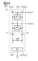
- FIG. 2A is a circuit diagram showing a configuration example of a semiconductor device
- FIGS. 2B and 2C are circuit diagrams showing a configuration example of a circuit included in the semiconductor device.
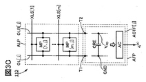
- 3A to 3C are circuit diagrams showing a configuration example and an operation example of the semiconductor device.
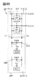
- 4A and 4B are circuit diagrams showing a configuration example and an operation example of the semiconductor device.
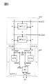
- FIG. 5 is a circuit diagram showing a configuration example of a semiconductor device.
- 6A to 6C are circuit diagrams showing a configuration example of a circuit included in the semiconductor device.
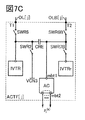
- 7A to 7C are circuit diagrams showing a configuration example of a circuit included in the semiconductor device.
- FIG. 8 is a circuit diagram showing a configuration example of the semiconductor device.
- FIG. 9 is a timing chart illustrating an operation example of the semiconductor device.
- FIG. 10 is a circuit diagram showing a configuration example of a circuit included in the semiconductor device.
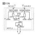
- 11A and 11B are circuit diagrams showing a configuration example of a circuit included in the semiconductor device.
- FIG. 12 is a circuit diagram showing a configuration example of a semiconductor device.
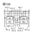
- 13A to 13D are circuit diagrams showing a configuration example of a circuit included in the semiconductor device.
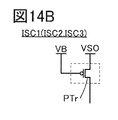
- 14A to 14C are circuit diagrams showing a configuration example of a circuit included in the semiconductor device.
- FIG. 15 is a circuit diagram showing a configuration example of a semiconductor device.
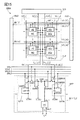
- FIG. 16 is a circuit diagram showing a configuration example of a semiconductor device.
- FIG. 16 is a circuit diagram showing a configuration example of a semiconductor device.
- 17 is a circuit diagram showing a configuration example of a semiconductor device.
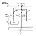
- 18A and 18B are circuit diagrams showing a configuration example of a circuit included in the semiconductor device.
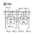
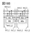
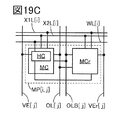
- 19A to 19E are circuit diagrams showing a configuration example of a circuit included in the semiconductor device.
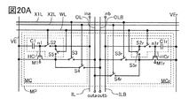
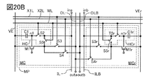
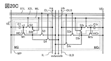
- 20A to 20C are circuit diagrams showing a configuration example of a circuit included in the semiconductor device.
- 21A and 21B are circuit diagrams showing a configuration example of a circuit included in the semiconductor device.
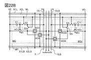
- 22A and 22B are circuit diagrams showing a configuration example of a circuit included in the semiconductor device.
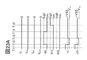
- 23A to 23C are timing charts for explaining an operation example of the semiconductor device.
- 24A to 24C are timing charts for explaining an operation example of the semiconductor device.
- 25A to 25C are timing charts for explaining an operation example of the semiconductor device.
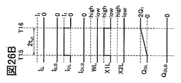
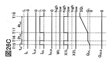
- 26A to 26C are timing charts for explaining an operation example of the semiconductor device.
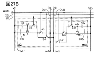
- 27A and 27B are circuit diagrams showing a configuration example of a circuit included in the semiconductor device.
- 28A and 28B are circuit diagrams showing a configuration example of a circuit included in the semiconductor device.
- 29A to 29C are circuit diagrams showing a configuration example of a circuit included in the semiconductor device.
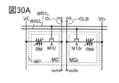
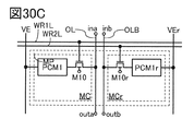
- 30A to 30C are circuit diagrams showing a configuration example of a circuit included in the semiconductor device.
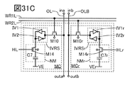
- 31A to 31C are circuit diagrams showing a configuration example of a circuit included in the semiconductor device.
- 32A and 32B are circuit diagrams showing a configuration example of a circuit included in the semiconductor device.
- FIG. 33 is a schematic cross-sectional view illustrating a configuration example of the semiconductor device.
- FIG. 34 is a schematic cross-sectional view illustrating a configuration example of the semiconductor device.
- 35A to 35C are schematic cross-sectional views illustrating a configuration example of the semiconductor device.
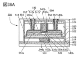
- 36A and 36B are schematic cross-sectional views illustrating a configuration example of a transistor.
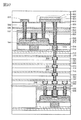
- FIG. 37 is a schematic cross-sectional view illustrating a configuration example of the semiconductor device.
- 38A and 38B are schematic cross-sectional views illustrating a configuration example of the transistor.
- FIG. 39 is a schematic cross-sectional view illustrating a configuration example of the semiconductor device.
- FIG. 40A is a top view showing a configuration example of the capacitance
- FIGS. 40B and 40C are cross-sectional perspective views showing a configuration example of the capacitance.
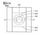
- FIG. 41A is a top view showing a configuration example of the capacitance
- FIG. 41B is a cross-sectional view showing a configuration example of the capacitance
- FIG. 41C is a sectional perspective view showing a configuration example of the capacitance.
- FIG. 42A is a diagram for explaining the classification of the crystal structure of IGZO
- FIG. 42B is a diagram for explaining the XRD spectrum of crystalline IGZO
- FIG. 42C is a diagram for explaining the microelectron diffraction pattern of crystalline IGZO.
- .. 43A is a perspective view showing an example of a semiconductor wafer
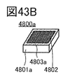
- FIG. 43B is a perspective view showing an example of a chip
- FIGS. 43C and 43D are perspective views showing an example of an electronic component.
- FIG. 44 is a perspective view showing an example of an electronic device.
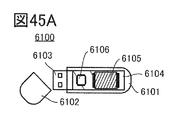
- 45A to 45C are perspective views showing an example of an electronic device.
- the synaptic connection strength can be changed by giving existing information to the neural network.
- the process of giving existing information to the neural network and determining the coupling strength may be called "learning”.
- the process of outputting new information based on the given information and the connection strength may be called “inference” or "cognition”.
- Examples of the neural network model include a Hopfield type and a hierarchical type.
- a neural network having a multi-layer structure may be referred to as a “deep neural network” (DNN), and machine learning by a deep neural network may be referred to as “deep learning”.
- DNN deep neural network
- a metal oxide is a metal oxide in a broad sense. Metal oxides are classified into oxide insulators, oxide conductors (including transparent oxide conductors), oxide semiconductors (also referred to as Oxide Semiconductor or simply OS) and the like.
- the metal oxide when a metal oxide is used in the active layer of a transistor, the metal oxide may be referred to as an oxide semiconductor. That is, when a metal oxide can form a channel forming region of a transistor having at least one of an amplification action, a rectifying action, and a switching action, the metal oxide is referred to as a metal oxide semiconductor, abbreviated as a metal oxide semiconductor. It can be called an OS. Further, when describing as an OS FET or an OS transistor, it can be paraphrased as a transistor having a metal oxide or an oxide semiconductor.
- a metal oxide having nitrogen may also be collectively referred to as a metal oxide. Further, a metal oxide having nitrogen may be referred to as a metal oxynitride.
- the configuration shown in each embodiment can be appropriately combined with the configuration shown in other embodiments to form one aspect of the present invention. Further, when a plurality of configuration examples are shown in one embodiment, the configuration examples can be appropriately combined with each other.
- the content (may be a part of the content) described in one embodiment is the other content (may be a part of the content) described in the embodiment and one or more other implementations. It is possible to apply, combine, or replace at least one content with the content described in the form of (may be a part of the content).
- the figure (which may be a part) described in one embodiment is different from another part of the figure, another figure (which may be a part) described in the embodiment, and one or more other figures.
- the figure (which may be a part) described in the embodiment is different from another part of the figure, another figure (which may be a part) described in the embodiment, and one or more other figures.
- a hierarchical neural network has one input layer, one or more intermediate layers (hidden layers), and one output layer, and is composed of a total of three or more layers.
- the hierarchical neural network 100 shown in FIG. 1A shows an example thereof, and the neural network 100 has a first layer to an R layer (R here can be an integer of 4 or more). ing.
- R can be an integer of 4 or more
- the first layer corresponds to the input layer
- the R layer corresponds to the output layer
- the other layers correspond to the intermediate layer.
- FIG. 1A shows the (k-1) th layer and the kth layer (k here is an integer of 3 or more and R-1 or less) as intermediate layers, and other intermediate layers. Is not shown.
- Each layer of the neural network 100 has one or more neurons.
- layer 1 has neurons N 1 (1) to neuron N p (1) (where p is an integer greater than or equal to 1), and layer (k-1) is neuron N 1. (K-1) to neuron N m (k-1) (where m is an integer of 1 or more), and the k-th layer has neurons N 1 (k) to neurons N n (k) ( Here, n is an integer of 1 or more), and the R layer has neurons N 1 (R) to neurons N q (R) (q here is an integer of 1 or more). ..
- FIG. 1B a neuron N j of the k-th layer (k), shows the signal which is input to the neuron N j (k), a signal output from the neuron N j (k), the.
- z 1 (k-1) to z m (k- ), which are output signals of neurons N 1 (k-1) to N m (k-1) in the (k-1) layer , respectively. 1) is output toward the neuron Nj (k) .
- the neuron N j (k) is, z 1 (k-1) to z m (k-1) to generate a z j (k) in response to, the z j (k) is an output signal (k + 1 ) Output to each neuron in the layer (not shown).
- the degree of signal transmission of signals input from neurons in the previous layer to neurons in the next layer is determined by the strength of synaptic connections (hereinafter referred to as weighting factors) that connect these neurons.
- weighting factors the strength of synaptic connections that connect these neurons.
- the signal output from the neurons in the previous layer is multiplied by the corresponding weighting factor and input to the neurons in the next layer.
- i an integer 1 or m
- the signal input to the neuron Nj (k) in the kth layer can be expressed by the equation (1.1).
- the result of the sum of products may be biased as a bias.
- the bias is b
- the equation (1.2) can be rewritten as the following equation.
- the neuron N j (k) produces an output signal z j (k) in response to u j (k) .
- Neuron N j output signal z j from (k) (k) defined by the following equation.
- the function f (u j (k) ) is an activation function in a hierarchical neural network, and a step function, a linear ramp function, a sigmoid function, or the like can be used.
- the activation function may be the same or different in all neurons.
- the activation function of neurons may be the same or different in each layer.
- the signal output by the neurons in each layer, the weighting coefficient w, or the bias b may be an analog value or a digital value.
- the digital value may be, for example, a binary value or a ternary value. A value with a larger number of bits may be used.
- an analog value for example, a linear ramp function, a sigmoid function, or the like may be used as the activation function.
- binary digital values for example, a step function with an output of -1 or 1 or 0 or 1 may be used.
- the signal output by the neurons in each layer may have three or more values.
- a step function that outputs -1, 0, or 1 or a step function that outputs 0, 1, or 2 may be used as the activation function that outputs three values.
- a step function that outputs -2, -1, 0, 1, or 2 may be used as an activation function that outputs five values.
- the circuit scale can be reduced, power consumption can be reduced, or the calculation speed can be increased. You can do things like that. Further, the accuracy of calculation can be improved by using analog values for at least one of the signal, the weighting coefficient w, or the bias b output by the neurons in each layer.
- the neural network 100 When the input signal is input to the first layer (input layer), the neural network 100 is sequentially input from the front layer in each layer from the first layer (input layer) to the last layer (output layer). Based on the signal, an output signal is generated using the equations (1.1), (1.2) (or equation (1.3)), and equation (1.4), and the output signal is used as the next layer. Perform the operation to output to.
- the signal output from the last layer (output layer) corresponds to the result calculated by the neural network 100.
- arithmetic circuit 1 ⁇ Configuration example of arithmetic circuit 1>
- the weighting coefficient of the synaptic circuit of the neural network 100 can be a digital value or an analog value of two or more values
- the activation function of the neuron is a step function or the like. be able to.
- weighting coefficient and the value of the signal input from the neuron in the previous layer to the neuron in the next layer is referred to as the first data. It may be called, and the other may be called the second data.
- the weighting coefficient and the calculated value of the synaptic circuit of the neural network 100 are not limited to digital values, and analog values can be used for at least one of them.
- the arithmetic circuit 110 shown in FIG. 2A is, for example, a semiconductor device having an array unit ALP and a circuit AFP. Arithmetic circuit 110, for example, by processing a signal input to the neuron N j (k) of the k-th layer in FIGS. 1A and 1B, neuron N j (k) output from the signal z j (k) Is a circuit that generates.
- the arithmetic circuit 110 may function as a storage device or a memory circuit.
- the arithmetic circuit 110 may function as a DRAM, SRAM, or flash memory as an example.
- the arithmetic circuit 110 may function as, for example, a circuit that performs calculations in a memory circuit, that is, an in-memory computing circuit.
- the array unit ALP has a circuit MP [1, j] to a circuit MP [m, j] as an example. Further, the circuit AFP has a circuit ACTF [j] as an example, and further, the circuit ACTF [j] has a capacitance CRE, a circuit AC, a terminal T1, and a terminal T2.
- the capacitive CRE may be realized by using a normal capacitive element, but one aspect of the present invention is not limited to this.
- the capacitance CRE may be realized by using the gate capacitance of the transistor as shown in FIG. 2B or FIG. 2C as an example.
- the transistor may use an N-channel type, a P-channel type, or both may be used and connected in parallel.
- a transistor CRET is used instead of the capacitance CRE.
- an OS transistor can be applied. The OS transistor will be described in detail in the fifth embodiment.
- a transistor having silicon in the channel forming region (hereinafter, referred to as a Si transistor) can be used.
- the silicon for example, single crystal silicon, hydrogenated amorphous silicon, microcrystalline silicon, polycrystalline silicon and the like can be used.
- transistors other than OS transistors and Si transistors include transistors with Ge as the active layer, transistors with compound semiconductors such as ZnSe, CdS, GaAs, InP, GaN, and SiGe as the active layer, and carbon nanotubes as the active layer.
- a transistor using an organic semiconductor as an active layer, or the like can be used.
- Each of the circuit MP [1, j] to the circuit MP [m, j] is electrically connected to the wiring OL [j] and the wiring OLB [j]. Further, each of the circuit MP [1, j] to the circuit MP [m, j] is electrically connected to the wiring XLS [1] to the wiring XLS [m]. Further, the wiring OL [j] is electrically connected to the terminal T1, the terminal T1 is electrically connected to the first terminal of the capacitance CRE, and the wiring OLB [j] is electrically connected to the terminal T2. , Terminal T2 is electrically connected to the second terminal of the capacitance CRE.
- some element or circuit may be connected between the terminal T1 and the first terminal of the capacitance CRE.
- some element or circuit may be connected between the terminal T2 and the second terminal of the capacitance CRE.
- each of the wiring XLS [1] to the wiring XLS [m] has signals z 1 (k-1) to z output from the neurons N 1 (k-1) to the neurons N m (k-1). It has a function of transmitting a potential corresponding to m (k-1) .
- Circuit MP [1, j] as an example, neurons N 1 (k-1) and the weighting coefficient w 1 (k-1) between the neurons N j (k) j (k ) ( first data here Similarly, the circuit MP [m, j] has a weighting coefficient w m ( as an example ) between the neuron N m (k-1) and the neuron N j (k). k-1) It has a function of holding j (k) .
- circuit MP [1, j] the signal z 1 (k-1) (here, the second data) and the first data w 1 (referred to as the second data ) output from the neuron N 1 (k-1). k-1) It has a function to output the product with j (k) .
- circuit MP [m, j] as an example, neurons N m (k-1) signal is output from the z m (k-1) (in this case the second data) and the first data w m (K-1) It has a function of outputting the product with j (k) .
- the potential corresponding to the second data z 1 (k-1) is input to the circuit MP [1, j] via the wiring XLS [1], so that the circuit MP [1, j] is input.
- information for example, current, voltage, etc.
- corresponding to the product of the first data w 1 (k-1) j (k) and the second data z 1 (k-1) is wired OL [j].
- the circuit MP [m, j] to the wiring XLS [m] that the potential is input in response to the second data z m (k-1) via the Then, the circuit MP [m, j] has information (for example, current, voltage, etc. ) according to the product of the first data w m (k-1) j (k) and the second data z m (k-1). ) Is output to the wiring OL [j] and / or the wiring OLB [j].
- information for example, current, voltage, etc.
- the information (for example, current, voltage, etc.) output from each of the circuit MP [1, j] to the circuit MP [m, j] is added.
- the information (for example, current, voltage, etc.) output from each of the circuits MP [1, j] to the circuit MP [m, j] is added. That is, the first data w 1 (k-1) j (k) to w m (k-1) j (k) and the second data z 1 (k-1) to each of the wiring OL and the wiring OLB.
- Information (for example, current, voltage, etc.) corresponding to the sum of products of z m (k-1) flows.
- information eg, current, voltage, etc.
- a reference for example, reference, precharge, bias, etc.
- the circuit ACTF [j] acquires information (for example, current, voltage, etc.) according to the sum of products of the first data and the second data from the wiring OL [j] and the wiring OLB [j]. It functions as a circuit that generates the signal z j (k) output from the neuron N j (k) .
- the output signal z j (k) (referred to as an calculated value ) represented by a digital value such as a binary value or a multi-valued value or an analog value based on the information by the circuit AC included in the circuit ACTF [j]. May be generated). That is, the circuit AC is treated as an activation function circuit as an example.
- the circuit AC may be, for example, an analog-to-digital conversion circuit (sometimes referred to as a sense amplifier or the like). Specifically, as an example, the circuit AC outputs a digital signal having a value of "0" as an output signal z j (k) when the result of the sum of products is "0" or less, and the result of the sum of products is When is "positive", it can be an analog-to-digital conversion circuit that outputs a "positive" digital value as an output signal z j (k) .
- each of the circuit MP [1, j] and the circuit MP [m, j] when each of the circuit MP [1, j] and the circuit MP [m, j] is not distinguished, it shall be described as the circuit MP.
- each of the wiring XLS [1] and the wiring XLS [m] is not distinguished, it is described as the wiring XLS.
- each [j] of the wiring OL [j] and the wiring OLB [j] may be omitted and described as the wiring OL and the wiring OLB.
- [j] of the circuit ACTF [j] may be omitted and described as the circuit ACTF.
- FIGS. 3A to 3C are circuit diagram showing the order of operation examples of the circuit ACTF [j].
- FIG. 3A shows an operation example of initializing the voltage between the first terminal and the second terminal of the capacitance CRE of the circuit ACTF [j] to 0V.
- Vini is given to each of the wiring OL [j] and the wiring OLB [j] as an initialization potential.
- Vini when a current flows from the wiring OL to the circuit MP, it becomes VDD, and when a current flows from the circuit MP to the wiring OL, it becomes VSS or GND.
- the first data w 1 (k-1) j (k) to w m (k-1) j (k) are obtained according to the circuits MP [1, j] to MP [m, j], respectively.
- Information for example, current, voltage, electric charge, etc.
- corresponding to the sum of products with the second data z 1 (k-1) to z m (k-1) is output to the wiring OL [j] and the wiring OLB [j].
- An operation example is shown in which the circuit ACTF [j] acquires the information.
- the potential V ini of the first terminal of the capacitor CRE is changed to the potential V OL based on the information input through the line OL [j] from the circuit MP in the circuit ACTF [j],
- the capacitor CRE It is assumed that the potential Vini of the second terminal of No. 2 changes to the potential VOLB based on the information input from the circuit MP to the circuit ACTF [j] via the wiring OLB [j].
- the first terminal of capacitor CRE - a voltage between the second terminal
- (
- corresponds to the difference between the total amount of information flowing through the wiring OL [j] and the total amount of information flowing through the wiring OLB [j].
- the voltage (charge) stored in the capacitance CRE is input to the circuit AC to sense the amount of voltage (charge) stored in the capacitance CRE.
- the potential V OL, and the potential V OLB depending on the result of multiply-add, varies greatly. Therefore, when the potential is input to the circuit AC as it is, there may be disadvantages such as the circuit configuration of the circuit AC becoming complicated and the operating range of the circuit AC becoming small. Therefore, as an example, the potential V OL, and also have different sizes of the potential V OLB, is their difference
- (
- 1 becomes,
- a reference potential here, a GND potential (0V) is used as an example.
- one aspect of the present invention is not limited to this, and may be a VDD potential, a precharge potential, a potential of (VDD / 2), or the like).
- the potential of either the first terminal of the capacitance CRE or the second terminal of the capacitance CRE can be set to
- the circuit AC senses the potential of the second terminal of the capacitance CRE and outputs a signal z j (k) corresponding to the voltage VRD . That is, according to the operation example shown in FIG. 3C, as a result of the sum of products of the first data and the second data output by the circuit MP [1, j] to the circuit MP [m, j], the signal z j ( k) is output.
- Each of the first data w 1 (k-1) j (k) to w m (k-1) j (k) is, for example, “+1”, “0”, “-1” for the sake of simplicity.
- each of the second data z 1 (k-1) to z m (k-1) is, for example, a value of "+1", "0", or "-1”. Shall be taken.
- line OL and the potential V ini applied to the wiring OLB, as a high-level potential, is assumed to be pre-charged.
- circuit MP when the product of the first data and the second data is "+1", the circuit MP and the wiring OL are in a conductive state, and the circuit MP and the wiring OLB are in a non-conducting state. It shall be. Then, it is assumed that a current corresponding to "
- the magnitude of the potential V OL is the product of the first data and the second data is determined by the number of circuit MP which is "+1". Specifically, the larger the number of circuit MPs in which the product of the first data and the second data is "+1", the more the circuit MP flows from the wiring OL to the circuit MP [1, j] to the circuit MP [m, j]. The total amount of current increases. Further, since the potential Vini , which is a high level potential, is precharged in the wiring OL, the larger the total amount of current flowing through the circuit MP [1, j] to the circuit MP [m, j], the larger the wiring OL. The voltage drop from the potential Vinii becomes large. That is, the larger the number of circuit MPs in which the product of the first data and the second data is “+1”, the lower the potential VOL .
- the magnitude of the potential VOLB is determined by the number of circuit MPs in which the product of the first data and the second data is “-1”. Specifically, the larger the number of circuit MPs in which the product of the first data and the second data is "-1”, the more the wiring OLB changes from the circuit MP [1, j] to the circuit MP [m, j]. The total amount of current that flows increases. Further, the wiring OLB is, the potential V ini is a high level potential is precharged circuit MP [1, j] to the circuit MP [m, j] the larger the current amount of the total flow in the wiring OLB The voltage drop from the potential Vinii becomes large. That is, the larger the number of circuit MPs in which the product of the first data and the second data is “-1”, the lower the potential VOLB .
- the number of circuit MPs in which the product of the first data and the second data is "+1" is larger than the number of circuit MPs in which the product of the first data and the second data is "-1".
- the potential V OL of the first terminal of the capacitor CRE is lower than the potential V OLB the second terminal of the capacitor CRE. That is, the product of the first data w 1 (k-1) j (k) to w m (k-1) j (k) and the second data z 1 (k-1) to z m (k-1). when the sum is "positive", the potential V OL is lower than the potential V OLB.
- the number of circuit MPs in which the product of the first data and the second data is "-1" is larger than the number of circuit MPs in which the product of the first data and the second data is "+1".
- the potential V OL of the first terminal of the capacitor CRE is higher than the potential V OLB the second terminal of the capacitor CRE. That is, the product of the first data w 1 (k-1) j (k) to w m (k-1) j (k) and the second data z 1 (k-1) to z m (k-1). when the sum is "negative", the potential V OL is higher than the potential V OLB.
- the potential V of the first terminal of the capacitance CRE is equal to the potential VOLB of the second terminal of the capacitance CRE. That is, the product of the first data w 1 (k-1) j (k) to w m (k-1) j (k) and the second data z 1 (k-1) to z m (k-1). when the sum is "0”, the potential V OL and the potential V OLB, at the same potential. Furthermore, in all, when the product of the first data and the second data is "0", the potential V OL and the potential V OLB, remains at potential V ini.
- the first data w 1 (k-1) j (k) to w m (k-1) j (k) are, for example, “+1”, “0”, and “ ⁇ ”, respectively.
- the operation of the semiconductor device according to one aspect of the present invention is not limited to this.
- the possible values of the first data w 1 (k-1) j (k) to w m (k-1) j (k) are set to “+2”, “+1”, “0”, “-1”. , "-2", etc., which may be a multi-value exceeding 3 values, or "+1", "-1", etc., which may be a 2-value value.
- the amount of current flowing between the circuit MP [1, j] to the circuit MP [m, j] and the wiring OL and / or the wiring OLB is the amount of the circuit MP [1, j] to the circuit MP [m, j]. If it is determined according to the result of the product of the possible values of the first data w 1 (k-1) j (k) to w m (k-1) j (k) held in each and the second data. Good. Specifically, for example, the first data w 1 (k-1) j (k) to w m (k-1) j (k) are "+2", "+1", "0", and "-", respectively.
- each of the second data z 1 (k-1) to z m (k-1) is either "+1", "0", or "-1".
- the circuit MP when the product of the first data and the second data is "+1", the circuit MP and the wiring OL are in a conductive state, and the circuit MP and the wiring OLB are in a non-conducting state. as that is, it is assumed that the current of the current amount I ut flows circuit MP from the wiring OL.
- the circuit MP when the product of the first data and the second data is "+2", the circuit MP and the wiring OL are in a conductive state, and the circuit MP and the wiring OLB are in a non-conducting state. as things may be assumed that current flows in the current amount 2 ⁇ I ut the circuits MP from the wiring OL. Further, when the product of the first data and the second data is "-1", the circuit MP and the wiring OL are in a non-conducting state, and the circuit MP and the wiring OLB are in a conductive state.
- the voltage between the first terminal and the second terminal of the first capacitance can be adjusted to the first data w 1 (k-1) j (k) to w m (k-1). ) corresponding to the sum of products and j (k) and the second data z 1 (k-1) to z m (k-1), the potential difference between the potential V OL and the potential V OLB (voltage
- V RD can do.
- the second terminal of the capacitance CRE may be electrically suspended (the first terminal of the capacitance CRE may also be electrically suspended), and then. , the potential of the first terminal of capacitor CRE to the GND potential, the potential of the second terminal of the capacitor CRE to V RD.
- the sum of products of the first data w 1 (k-1) j (k) to w m (k-1) j (k) and the second data z 1 (k-1) to z m (k-1) is If it is "positive", the potential V RD of the second terminal of the capacitor CRE becomes a positive potential, the first data w 1 (k-1) j (k) to w m (k-1) and j (k) If the product sum between the second data z 1 (k-1) to z m (k-1) is "negative", the potential V RD of the second terminal of the capacitor CRE becomes a negative potential.
- the circuit AC by sensing the potential of the second terminal of capacitor CRE, can output an output signal z j (k) corresponding to the voltage V RD. That is, the potential V OL of the first terminal of capacitor CRE, even if the potential V OLB the second terminal of the capacitor CRE each other large or, the potential V OL of the first terminal of capacitor CRE, the second capacitor CRE even if the electric potential V OLB terminals together small, equal when the difference voltage between the potential V OL and the potential V OLB is respectively, by detecting the difference voltage by capacitive CRE, circuit AC voltage of the same magnitude The same result can be output as an output signal z j (k) . As a result, it is possible without depending on the magnitude of the potential V OL and the potential V OLB, to obtain more accurate product-sum results.
- the circuit AC may be an activation function circuit, and depending on the type of activation function, for example, the result of the sum of products of the first data and the second data is "0".
- a digital signal having a value of "0" is output as the output signal z j (k)
- the output signal is output.
- a circuit capable of outputting a "positive" multi-value as z j (k) may be used.
- an analog-digital conversion circuit sense amplifier, comparator, etc.
- the information held in the memory cell to be read is read by outputting the signal from the memory cell to be read to the wiring OL and outputting the signal from the memory cell for reference to the wiring OLB.
- It may be used as a function. That is, it may be used as a DRAM, SRAM, or flash memory. For example, it may be operated as a reading of multi-valued data.
- it may be used as a circuit that performs calculations in a memory circuit, that is, an in-memory computing circuit.
- the circuit AC is positive.
- An analog-to-digital conversion circuit or the like capable of sensing a negative voltage in addition to the above voltage may be used.
- the potential of the first terminal of the capacitance CRE may be set to (VDD / 2) instead of the potential of the first terminal of the capacitance CRE as the GND potential. In this way, when the result of the sum of products of the first data and the second data is "zero", the circuit AC is input with the potential of (VDD / 2).
- the circuit AC is input with a positive potential. Will be done.
- an analog-digital conversion circuit sense amplifier, comparator, etc.
- the analog-digital conversion circuit can be simplified when the input voltage is only a positive voltage. That is, since a negative power supply voltage is not required, the power supply circuit can be simplified.
- the range of the input voltage can be widened, a large margin for noise can be taken, and accurate processing can be performed.
- a method of outputting a "negative” multi-value as the output signal zj (k) is, for example, .
- the arithmetic circuit 110 of FIG. 2A may be changed to the arithmetic circuit 120 shown in FIG. 4A.
- analog-digital conversion circuits sense amplifiers, comparators, etc.
- the arithmetic circuit 120 has a capacitance CREP, a capacitance CREM, a circuit ACP, and a circuit ACM.
- the first terminal of the capacitance CREP is electrically connected to the terminal T1
- the second terminal of the capacitance CREP is electrically connected to the terminal T2.
- the first terminal of the capacitance CREM is electrically connected to the terminal T1
- the second terminal of the capacitance CREM is electrically connected to the terminal T2.
- some element or circuit for example, a switch, a transistor, etc. may be connected between the terminal T1 and the first terminal of the capacitance CREP (capacity CREM).
- the circuit ACP and the circuit ACM are analog-to-digital conversion circuits (sense amplifier, comparator, etc.) capable of sensing a positive voltage, for example, like the circuit AC used in the arithmetic circuit 110 of FIG. 2A. It is assumed that each of the circuit ACP and the circuit ACM is initialized before sensing, the circuit ACP senses the potential of the second terminal of the capacitance CREP, and the circuit ACM is the potential of the first terminal of the capacitance CREM. Sensing. That is, the sensing terminal is changed between the capacitance CREP and the capacitance CREM.
- Calculation circuit 120 of FIG. 4A similarly to the operation example of FIGS. 3A and 3B, the potential of the wiring OL and V OL, the potential of the wiring OL as V OLB, the first terminal of the capacitor CREP - between the second terminal
- the potential of the wiring OL and V OL
- V OLB the potential of the wiring OL as V OLB
- each of the second terminal of the capacitance CREP and the first terminal of the capacitance CREM is electrically suspended (the first terminal of the capacitance CREP and the second terminal of the capacitance CREM are also provided. It may be electrically suspended), and then the potentials of the first terminal of the capacitance CREP and the second terminal of the capacitance CREM are set to the GND potentials.
- the second potential V RD next terminal of the capacitor CREP the potential of the first terminal of the capacitor CREM becomes -V RD.
- circuit ACM since the potential -V RD of the first terminal of the capacitor CREM is negative, not performed the output potential from the circuit ACM (or zero is output), circuit ACP, since is positive potential V RD of the second terminal of the capacitor CREP, perform sensing, outputs a potential corresponding the circuit ACP to the potential V RD.
- circuit ACP since the potential V RD of the second terminal of the capacitor CREP is negative, not performed the output potential from the circuit ACP (or zero is output), the circuit Since the potential ⁇ V RD of the first terminal of the capacitance CREM is positive in the ACM, sensing is performed and the potential corresponding to the potential V RD is output from the circuit ACM.
- the circuit ACP does not output the potential (or zero is output) because the potential of the first terminal of the capacitance CREP is the GND potential, and also. Since the potential of the second terminal of the capacitance CREM of the circuit ACM is the GND potential, the potential is not output from the circuit ACM (or zero is output).
- the potential output from the circuit ACP corresponds to the "positive” multi-value and the potential output from the circuit ACM correspond to the "negative” multi-value, an analog capable of sensing only a positive voltage. Even when a digital conversion circuit (sense amplifier, comparator, etc.) is used, even if the result of the sum of products of the first data and the second data is "negative", the output signal zj (k) is "negative". It is possible to output multiple values of.
- the circuit AC in FIG. 4, an example in which the circuit ACP and the circuit ACM are provided is shown, but one aspect of the present invention is not limited to this.
- the circuit ACP and the circuit ACM may be the circuit AC only, and the circuit AC may perform sensing twice. That is, the operation of the circuit AC may be divided into two times and operated in a time division manner. As a result, the processing time becomes long, but the scale of the circuit can be reduced.
- FIG. 5 is a circuit that generates a signal z j (k) according to a current input from the wiring OL [j] and the wiring OLB [j].
- FIG. 5 shows an example of an arithmetic circuit that outputs an output signal z j (k) represented by a multi-valued or analog value. Therefore, the circuit ACTF [j] can be configured to have a function as an activation function circuit in a neural network as an example.
- FIG. 5 also shows the array unit ALP and the circuit AFP in order to show the configuration of the electrical connection between the circuit ACTF [j] and the peripheral circuits.
- the circuit ACTF [j] shown in FIG. 5 has, as an example, a switch SWR1, a switch SWR1B, a switch SWR2, a switch SWR2B, a circuit IVTR, a circuit IVTRr, a capacitance CRE, and a circuit AC.
- an electric switch such as an analog switch or a transistor
- the transistor can be a transistor that can be used for the transistor CRET.
- a mechanical switch may be applied.
- the circuit IVTR is electrically connected to the terminal T1 and the first terminal of the switch SWR1.
- the second terminal of the switch SWR1 is electrically connected to the first terminal of the capacitance CRE and the first terminal of the switch SWR2.
- the second terminal of the switch SWR2 is electrically connected to the wiring VCN3.
- the circuit IVTRr is electrically connected to the terminal T2 and the first terminal of the switch SWR1B.
- the second terminal of the switch SWR1B is electrically connected to the second terminal of the capacitance CRE and the first terminal of the switch SWR2B.
- the second terminal of the switch SWR2B is electrically connected to the terminal mbt1 of the circuit AC.
- Wiring VCN3 functions as wiring that gives a constant voltage.
- the constant voltage can be, for example, a ground potential GND or a low level potential.
- VDD high level potential
- the circuit AC has a terminal mbt1 and a terminal mbt2.
- an analog-to-digital conversion circuit or the like can be used as an example.
- Circuit AC shown in Figure 5 to sense the potential supplied to terminal MBT1, having as a digital signal, from the terminal mbt2 function of outputting an output signal z j (k) in accordance with the potential. Therefore, for example, in the case of an analog-to-digital conversion circuit that converts the circuit AC into a 1-bit digital signal, the number of terminals mbt2 is one, and the circuit AC is, for example, k bits (k is an integer of 2 or more).
- the number of terminals 2 is k.
- the terminal mbt2 is shown as a plurality of terminals.
- the circuit AC performs analog-to-digital conversion with reference to a plurality of predetermined potentials, converts the analog potential (or multi-valued digital value) of the terminal mbt1 into a digital signal, and outputs it.
- the circuit ACTF [j] of FIG. 5 when the circuit ACTF [j] of FIG. 5 is applied as a circuit of the activation function of neurons in a hierarchical neural network, for example, in the analog digital conversion, the potential of the terminal mbt1 of the circuit AC is changed.
- the potential is lower than the potential given by the wiring VCN3 (when the result of the sum of products of the first data and the second data is negative), the configuration is such that zero is output instead of the value.
- the circuit of the activation function can operate as a circuit that outputs the value of the step function.
- the circuit IVTR is a circuit having a function of converting the current flowing through the wiring OL [j] into a voltage value (or an amount of electric charge). Further, the circuit IVTRr is a circuit having a function of converting the current flowing through the wiring OLB [j] into a voltage value (or an amount of electric charge), and can have the same configuration as the circuit IVTR.
- the circuit IVTR converts the current flowing through the wiring OL [j] into a voltage value (or charge amount) and gives the voltage value to the first terminal of the switch SWR1.
- the circuit IVTRr can convert the current flowing through the wiring OLB [j] into a voltage value (or charge amount) and give the voltage value to the first terminal of the switch SWR1B.
- the circuit IVTR (circuit IVTRr) can have, for example, the circuit configuration shown in FIGS. 6A to 6C.
- the reference numerals of the wiring OLB [j] and the circuit elements included in the circuit IVTRr are shown in parentheses in FIGS. 6A to 6C.
- the circuit IVTR (circuit IVTRr) shown in FIG. 6A has a switch SWR3 (switch SWR3B) and a capacitance CRT (capacity CRTB).
- the wiring OL [j] (wiring OLB [j]) is electrically connected to the first terminal of the switch SWR3 (switch SWR3B) and the first terminal of the capacitance CRT (capacity CRTB).
- the second terminal of the switch SWR3 (switch SWR3B) is electrically connected to the second terminal of the capacitance CRT (capacity CRTB) and the wiring VCN4.
- switch SWR3 and the switch SWR3B for example, a switch that can be applied in the same manner as the above-mentioned switch SWR1, switch SWR1B, switch SWR2, and switch SWR2B can be used.
- Wiring VCN4 functions as wiring that gives a constant voltage, for example.
- the constant voltage can be, for example, a high level potential, a ground potential, or a low level potential.
- the wiring VCN4 may be given the same potential as the wiring VSO described later.
- the wiring VCN4 may be electrically connected to the wiring VSO. That is, the wiring VCN4 and the wiring VSO may be combined into one wiring.
- the switch SWR3 switch SWR3B
- the constant voltage of the wiring VCN4 can be applied to the wiring OL [j] (wiring OLB [j]).
- the operation of applying a constant voltage of the wiring VCN4 to the wiring OL [j] (wiring OLB [j]) is for reading information (current, voltage, etc.) from the circuit MP [1, j] to the circuit MP [m, j]. Corresponds to the initial operation.
- circuit IVTR circuit IVTRr
- switch SWR3B switch SWR3B
- the amount of current flowing through the wiring OL [j] (wiring OLB [j]) is used as an electric charge for the capacitance CRT.
- the first terminal can be charged. That is, the potential of the first terminal of the capacitance CRT is determined according to the amount of current flowing through the wiring OL [j] (wiring OLB [j]).
- the amount of current flowing through the wiring OL [j] is, for example, the circuit MP [1, j] to the circuit MP [m, j] and the wiring OL [j] (wiring OLB [j]).
- the current flowing between each of the circuits MP [1, j] to the circuit MP [m, j] and the wiring OL [j] (wiring OLB [j]) is allowed to flow for a certain period of time.
- the electric charge charged to the first terminal of the capacitance CRT is determined by the amount of current flowing through the wiring OL [j] (wiring OLB [j]) and the fixed time.
- the voltage applied by the circuit IVTRr (circuit IVTRr) to the first terminal of the switch SWR1 (switch SWR1B) is determined by the amount of current and the time passed by each of the circuit MP [1, j] to the circuit MP [m, j]. Be done.
- the circuit IVTR ( The circuit IVTRr) can have the circuit configuration shown in FIG. 6B. That is, the capacitance CRT (capacity CRTB) can be omitted in the circuit IVTR (circuit IVTRr) of FIG. 6A.
- the circuit IVTR (circuit IVTRr) shown in FIG. 6C has a switch SWR3 (switch SWR3B) and a resistor RRT (resistor RRTB).
- the wiring OL [j] (wiring OLB [j]) is electrically connected to the first terminal of the switch SWR3 (switch SWR3B) and the first terminal of the resistor RRT (resistor RRTB).
- the second terminal of the switch SWR3 (switch SWR3B) is electrically connected to the second terminal of the resistor RRT (resistor RRTB) and the wiring VCN4.
- the circuit IVTR (circuit IVTRr) shown in FIG. 6C turns on the switch SWR3 (switch SWR3B) to bring the wiring OL [j] (wiring OLB [j]) and the wiring VCN4 into a conductive state.
- the constant voltage of the wiring VCN4 can be applied to the wiring OL [j] (wiring OLB [j]).
- the operation of applying a constant voltage of the wiring VCN4 to the wiring OL [j] (wiring OLB [j]) is for reading information (current, voltage, etc.) from the circuit MP [1, j] to the circuit MP [m, j]. Corresponds to the initial operation. Further, in the circuit IVTR (circuit IVTRr) shown in FIG.
- the potential of the first terminal of the capacitance CRT is determined according to the amount of current flowing through the wiring OL [j] (wiring OLB [j]) and the resistance value of the resistor RRT (resistor RRTB).
- the switch SWR3 does not necessarily have to be provided.
- the circuit ACTF [j] shown in FIG. 7A is a configuration example in which the circuit configuration of the circuit ACTF [j] shown in FIG. 5 is changed. Specifically, the circuit ACTF [FIG. 5] shows that the terminal mbt1 of the circuit AC is electrically connected to the second terminal of the switch SWR2, and the wiring VCN3 is electrically connected to the second terminal of the switch SWR2B. j] is different.
- the circuit ACTF [j] of FIG. 7B includes a switch SWR2, a switch SWR2B, a switch SWR6, a switch SWR6B, a switch SWR7, a switch SWR7B, a capacitance CRE, a circuit IVTR, a circuit IVTRr, and a circuit AC.
- the first terminal of the switch SWR6 is electrically connected to the terminal T1, and the second terminal of the switch SWR6 is connected to the first terminal of the switch SWR7, the first terminal of the switch SWR2, and the first terminal of the capacitance CRE. It is electrically connected.
- the second terminal of the switch SWR7 is electrically connected to the circuit IVTR, and the second terminal of the switch SWR2 is electrically connected to the wiring VCN3.
- the first terminal of the switch SWR6B is electrically connected to the terminal T2, and the second terminal of the switch SWR6B is connected to the first terminal of the switch SWR7B, the first terminal of the switch SWR2B, and the second terminal of the capacitance CRE. It is electrically connected.
- the second terminal of the switch SWR7B is electrically connected to the circuit IVTRr, and the second terminal of the switch SWR2B is electrically connected to the circuit AC.
- switch SWR6B As each of the switch SWR6, the switch SWR6B, the switch SWR7, and the switch SWR7B, for example, a switch that can be applied in the same manner as the above-mentioned switch SWR1, switch SWR1B, switch SWR2, and switch SWR2B can be used.
- the circuit ACTF [j] shown in FIG. 7C can be used as a circuit configuration applicable to the circuit ACTF [j] of FIG. 2A.
- the circuit ACTF [j] of FIG. 7C has a configuration in which the switch SWR7 and the switch SWR2B are not provided in the circuit ACTF [j] of FIG. 7B. That is, in the circuit ACTF [j] of FIG. 7C, the second terminal of the switch SWR6 is electrically connected to the circuit IVTR, and the terminal mbt1 of the circuit AC is the second terminal of the capacitance CRE and the second terminal of the switch SWR6B. Is electrically connected to the first terminal of the switch SWR7B.
- the first data and the second data are similar to the circuit ACTF [j] of FIG.
- the signal z j (k) can be output.
- ⁇ Operation example 2 of arithmetic circuit> an operation example of the circuit ACTF [j] of FIG. 5 will be described.
- the arithmetic circuit 110A shown in FIG. 8 is used as an example.
- the arithmetic circuit 110A has a configuration in which the circuit IVTR (circuit IVTRr) of FIG. 6A is applied as the circuit IVTR and the circuit IVTRr included in the circuit ACTF [j] shown in FIG.
- the switch SWR1, the switch SWR2, the switch SWR3, the switch SWR1B, the switch SWR2B, and the switch SWR3B included in the circuit ACTF [j] are switched between the on state and the off state.
- Wiring SRL1, wiring SRL2-1, wiring SRL2-2, and wiring SRL3 are shown as wirings for this purpose.
- the wiring SRL1 is electrically connected to the control terminal of the switch SWR1 and the control terminal of the switch SWR1B
- the wiring SRL2-1 is electrically connected to the control terminal of the switch SWR2.
- the switch SWR1, the switch SWR2, the switch SWR3, the switch SWR1B, the switch SWR2B, or the switch SWR3B may be partially omitted depending on the situation or the situation. That is, for example, the switch SWR1, the switch SWR2, the switch SWR1B, and the switch SWR2B may have a circuit configuration in which some of the switches are always on. Further, for example, by using another switch, the switch SWR3 and the switch SWR3B may have a circuit configuration in which a part of those switches is always in the off state.
- the switch SWR1, the switch SWR2, the switch SWR3, the switch SWR1B, the switch SWR2B, and the switch SWR3B can be partially changed in the connection configuration.
- the wiring SRL1, the wiring SRL2-1, the wiring SRL2-2, or the wiring SRL3 may be partially omitted depending on the situation or the situation.
- the wiring SRL2-1 and the wiring SRL2-2 may be combined into one wiring.
- the wiring SRL1 and the wiring SRL2-1 (wiring SRL2-2) may be combined into one wiring by reversing the on / off polarities of the switch SWR1 and the switch SWR2 (switch SWR2B). ..
- the switch SWR1 and the switch SWR2 (switch SWR2B) can be alternately turned on and off with a single wire.
- FIG. 8 shows a node n4 as an electrical connection point between the first terminal of the switch SWR1, the first terminal of the capacitance CRT, and the first terminal of the switch SWR3, and the first terminal of the switch SWR1B.
- the node n4r is shown as an electrical connection point between the first terminal of the capacitance CRTB and the first terminal of the switch SWR3B.
- node n5 is shown as an electrical connection point between the second terminal of the switch SWR1, the first terminal of the capacitance CRE, and the first terminal of the switch SWR2, and the second terminal of the switch SWR1B and the capacitance CRE are shown.
- Node n5r is illustrated as an electrical connection point between the second terminal and the first terminal of the switch SWR2B.
- FIG. 9 is a timing chart showing an operation example of the circuit ACTF [j] of the arithmetic circuit 110A of FIG. 8, and the timing chart shows the wiring XLS [1] between the time T01 and the time T08 and in the vicinity thereof.
- ACTF [j] of the arithmetic circuit 110A of FIG. 8 shows the wiring XLS [1] between the time T01 and the time T08 and in the vicinity thereof.
- High in FIG. 9 indicates a high level potential, and low indicates a low level potential.
- each of the switch SWR1, the switch SWR2, the switch SWR1B, and the switch SWR2B is turned on when a high level potential is input to the control terminal, and when a low level potential is input to the control terminal. It shall be turned off.
- the timing chart of FIG. 9 collectively shows the wiring XLS [1] to the wiring XLS [m]. Further, in the timing chart of FIG. 9, the period during which the second data is input to the wiring XLS [1] to the wiring XLS [m] is indicated by hatching.
- the constant voltage given by the wiring VCN4 is defined as VDD (high level potential).
- the amount of current flowing from the wiring OL [j] to the circuit MP and the amount of current flowing from the wiring OLB [j] to the circuit MP are the first data held in the circuit MP and the second data input from the wiring XLS. It depends on the data. Further, the amount of current flowing from the wiring OL [j] to the circuit MP and / or the amount of current flowing from the wiring OLB [j] to the circuit MP may be zero.
- the constant voltage given by the wiring VCSN3 is defined as VSS.
- the weighting coefficients w 1 (k-1) j (k) to w m (k-1 ) are used as the first data for each of the circuits MP [1, j] to MP [m, j]. ) It is assumed that j (k) is retained.
- each potential of the node n4, the node n4r, the node n5, and the node n5r is defined as VSS.
- a high level potential is input to the wiring SRL1 and the wiring SRL3 between the time T01 and the time T02.
- the switch SWR1 and the switch SWR1B are turned on, and when the high level potential is input to the wiring SRL3, the switch SWR3 and the switch SWR3B are turned on.
- a low level potential is input to the wiring SRL2-1 and the wiring SRL2-2.
- the switch SWR2 and the switch SWR2B are turned off.
- the wiring between the wiring VCN4 and the wiring OL [j] and the wiring between the wiring VCN4 and the first terminal of the capacitance CRE become conductive. Further, a conductive state is established between the wiring VCN4 and the wiring OLB [j], between the wiring VCN4 and the second terminal of the capacitance CRE, and between the wiring VCN4 and the terminal mbt1. Further, the wiring VCN3 and the first terminal of the capacitance CRE are in a non-conducting state. Therefore, the potentials of the nodes n4, the node n4r, the node n5, and the node n5r are VDD.
- a low level potential is input to the wiring SRL3 between the time T02 and the time T03.
- the switch SWR3 and the switch SWR3B are turned off. Therefore, the wiring VCN4 and the wiring OL [j] are in a non-conducting state, the wiring VCN4 and the wiring OLB [j] are in a non-conducting state, and the nodes n4, the node n5, the node n4r, and the node n5r It becomes a floating state.
- the circuit MP [i, j] in, depending on the weight coefficient w i (k-1) j (k) and neurons of the signal z 1 (k-1), wiring OL [j] or wiring OLB [j ], A current flows between the circuit MC, and a current flows between the other of the wiring OL [j] or the wiring OLB [j] and the circuit MCr.
- the sum of the currents flowing between each of the circuits MP [1, j] to the circuits MP [m, j] and the wiring OL [j] is defined as I out [j]
- a low level potential is input to the wiring SRL1.
- the switch SWR1 and the switch SWR1B are turned off. Therefore, the first terminal of the capacitance CRE and the wiring OL [j] are in a non-conducting state, and the second terminal of the capacitance CRE and the wiring OLB [j] are in a non-conducting state.
- the decrease in potential at the first terminal (node n5) of the capacitance CRE is stopped, and the decrease in potential at the second terminal (node n5r) of the capacitance CRE is stopped.
- the voltage between the first terminal (node n5) of the capacitance CRE and the second terminal (node n5r) of the capacitance CRE is held.
- the potentials of the node n4 and the node n4r continue to decrease from before time T04.
- a low level potential is input to each of the wiring XLS [1] and the wiring XLS [m].
- the current flowing from the wiring OL [j] to the circuit MP is stopped, and the current flowing from the wiring OLB [j] to the circuit MP is stopped. Therefore, the decrease in the potential of each of the node n4 and the node n4r stops.
- a high level potential is input to the wiring SRL2-1 between the time T06 and the time T07.
- the switch SWR2 is turned on. Therefore, the first terminal of the capacitance CRE and the wiring VCN3 are in a conductive state, and the potential of the first terminal (node n5) of the capacitance CRE becomes VSS.
- the potential of the first terminal (node n5) of the capacitance CRE changes from VIout to VSS, so that the second terminal of the capacitance CRE (node n5r) is coupled.
- the potential of the terminal (node n5r) also changes.
- the amount of change in potential due to capacitive coupling is determined according to the capacitive coupling coefficient, but in this specification and the like, for the sake of simplicity, when the potential of the first terminal of the capacitive CRE changes from VIout to VSS.
- the potential of the second terminal of the capacitor the CRE, V IBout - (in the timing chart of FIG. 9, V OP and notation) (V Iout -VSS) shall be changed to. That is, this change in potential corresponds to the case where the capacitive coupling coefficient determined according to the capacitive CRE and surrounding circuit elements is set to 1.
- a high level potential is input to the wiring SRL2-2 between the time T07 and the time T08.
- the switch SWR2B is turned on. Therefore, the second terminal (node n5r) of the capacitance CRE and the terminal mbt1 are in a conductive state.
- V OP which is the potential of the second terminal (node n5r) of the capacitance CRE, is input to the terminal mbt1 of the circuit AC.
- the circuit AC outputs a signal having a value of z j (k) as a digital signal corresponding to the potential V OP input to the terminal mbt1.
- z j (k) is the potential V Iout corresponding to the amount of current flowing through the wire OL [j], wiring OLB and the potential V IBout corresponding to the amount of current flowing through the [j], which is output based on the potential difference values Is. That is, the potential V Iout, potential V IBout includes a I out [j] and I Bout [j], the time that the switch SWR1 and the switch SWR2 is turned on (period from time T03 to time T04), by It can be decided.
- I out [j] and I Bout [j] are the first data w 1 (k-1) which are the first data held in each of the circuits MP [1, j] and the circuit MP [m, j].
- the values of z j (k) are obtained by converting each of the current amounts I out [j] and I Bout [j] into potentials and inputting the potential differences between them into the circuit AC. It is output.
- equivalent circuit AC by the circuit of the activation function in the hierarchical neural network, the z j (k) value of the output z j as a digital signal (k) is the formula (1.4) Can be the potential to be.
- the potential input to the terminal mbt1 is from V OP in consideration of the influence of the parasitic resistance and the parasitic capacitance. May fluctuate.
- the circuit AC is designed so as to appropriately correct the potential input to the terminal mbt1 in consideration of the resistance of the wiring between the second terminal of the capacitance CRE and the terminal mbt1.
- a configuration circuit AC may output a digital signal corresponding to the output signal z 0 as j (k) to the terminal MBT2. This corresponds to the activation function f (u j (k) ) in the hierarchical neural network functioning as a ramp function that outputs 0 when uji (k) is negative.
- one aspect of the present invention is not limited to the circuit configuration of the circuit ACTF [j] of FIG. 5 included in the arithmetic circuit.
- the circuit ACTF [j] of FIG. 5 included in the semiconductor device (arithmetic circuit) of one aspect of the present invention can be changed to the circuit configuration shown in the circuit ACTF [j] of FIG.
- the circuit ACTF [j] of FIG. 10 includes a switch SWR1, a switch SWR1B, a switch SWR2, a switch SWR2B, a switch SWR3, a switch SWR3B, a switch SWR4, a switch SWR4B, a load LE, and a load LEB. It has an operational unit OP, an operational unit OPB, and a circuit AC. The description of the portion overlapping with the circuit ACTF [j] shown in FIG. 5 will be omitted.
- Each of the switch SWR3, the switch SWR3B, the switch SWR4, and the switch SWR4B can be a switch that can be applied in the same manner as the switch SWR1, the switch SWR1B, the switch SWR2, and the switch SWR2B.
- the first terminal of the switch SWR3 is electrically connected to the terminal T1, the first terminal of the switch SWR4, and the first terminal of the load LE.
- the second terminal of the switch SWR3 is electrically connected to the wiring VCN4.
- the non-inverting input terminal of the operational amplifier OP is electrically connected to the wiring Vref1L
- the inverting input terminal of the operational amplifier OP is electrically connected to the second terminal of the switch SWR4
- the output terminal of the operational amplifier OP is the first load LE. It is electrically connected to the two terminals and the first terminal of the switch SWR1.
- the first terminal of the switch SWR3B is electrically connected to the terminal T2, the first terminal of the switch SWR4B, and the first terminal of the load LEB.
- the first terminal of the switch SWR3B is electrically connected to the wiring VCN4.
- the non-inverting input terminal of the operational amplifier OPB is electrically connected to the wiring Vref2L
- the inverting input terminal of the operational amplifier OPB is electrically connected to the second terminal of the switch SWR4B
- the output terminal of the operational amplifier OPB is the first of the load LEB. It is electrically connected to the two terminals and the first terminal of the switch SWR1B.
- the wiring Vref1L and the wiring Vref2L here function as wirings that supply the same voltage or different voltages from each other. Therefore, the wiring Vref1L and the wiring Vref2L may be combined into one wiring.
- the circuit ACTF [j] of FIG. 10 turns on the switch SWR3 (switch SWR3B) and turns off the switch SWR4 (switch SWR4B), thereby turning the wiring OL [j] (wiring OLB [j]) as in FIG.
- the initial operation of applying a constant voltage of the wiring VCN4 to j]) can be performed.
- the load LE and the load LEB can be, for example, a resistor, a capacitance, or the like.
- the operational amplifier OP and the load LE, and the operational amplifier OPB and the load LEB each function as an integrating circuit. That is, by turning off the switch SWR3 and the switch SWR3B and turning the switch SWR4 and the switch SWR4B on, the respective capacities (load LE) according to the amount of current flowing through the wiring OL [j] or the wiring OLB [j].
- Load LEB) stores electric charge. That is, the currents flowing from the wirings OL [j] and OLB [j] are converted into voltages by the integrating circuit, and the respective voltages are output from the output terminals of the operational amplifier OP and the operational amplifier OPB.
- the circuit ACTF [j] of FIG. 10 converts the amount of electric charge flowing through the wiring OL [j] into a voltage value, and transfers the voltage value to the first terminal of the switch SWR1. Further, the amount of electric charge flowing through the wiring OLB [j] can be converted into a voltage value, and the voltage value can be given to the first terminal of the switch SWR1B.
- the circuit ACTF [j] of FIG. 5 can be changed to the circuit configuration shown in the circuit ACTF [j] of FIG. 11A.
- the circuit ACTF [j] of FIG. 11A has a switch SWR3, a switch SWR3B, a switch SWR4, a switch SWR4B, a switch SWR5, a load LEA, a load LEAB, an operational amplifier OPA, and a circuit AC.
- Each of the switch SWR3, the switch SWR3B, the switch SWR4, the switch SWR4B, and the switch SWR5 can be a switch that can be applied in the same manner as the switch SWR1, the switch SWR1B, the switch SWR2, and the switch SWR2B.
- the first terminal of the switch SWR3 is electrically connected to the terminal T1, the first terminal of the switch SWR4, and the first terminal of the load LEA.
- the second terminal of the switch SWR3 is electrically connected to the wiring VCN4.
- the inverting input terminal of the operational amplifier OP is electrically connected to the second terminal of the switch SWR4.
- the second terminal of the load LEA is electrically connected to the first terminal of the switch SWR5.
- the first terminal of the switch SWR3B is electrically connected to the terminal T2, the first terminal of the switch SWR4B, and the first terminal of the load LEAB.
- the second terminal of the switch SWR3B is electrically connected to the wiring VCN4.
- the non-inverting input terminal of the operational amplifier OP is electrically connected to the second terminal of the switch SWR4B.
- the second terminal of the load LEAB is electrically connected to the wiring VCN5.
- the output terminal of the operational amplifier OP is electrically connected to the second terminal of the switch SWR5 and the terminal mbt1 of the circuit AC.
- the wiring VCN5 functions as wiring that applies a constant voltage.
- the constant voltage can be, for example, a ground potential or a low level potential.
- the circuit ACTF [j] of FIG. 11A turns on the switch SWR3 (switch SWR3B), turns off the switch SWR4 (switch SWR4B), and turns off the switch SWR5, thereby turning the wiring OL in the same manner as in FIG.
- the initial operation of applying a constant voltage of the wiring VCN4 to [j] can be performed.
- the load LEA and the load LEAB can be, for example, a resistor, a capacitance, or the like.
- a resistor can be used as the load LEA and the load LEAB.
- the voltage corresponding to the difference in the current flowing between the first terminal and the second terminal of the load LEA and between the first terminal and the second terminal of the load LEAB is set to the operational amplifier. It can be output from the output terminal of OPA.
- the switch SWR3 and the switch SWR3B are turned off, the switch SWR4 and the switch SWR4B are turned on, and the switch SWR5 is turned on, so that the current flowing through each of the wiring OL [j] and the wiring OLB [j]
- the voltage corresponding to the difference can be output from the output terminal of the optotype OPA.
- the voltage output from the output terminal of the operational amplifier OPA is input to the input terminal of the circuit AC.
- the analog voltage output from the output terminal of the operational amplifier OPA can be converted into a digital signal by the circuit AC.
- the digital signal is a calculated value z j (k) of the neurons of the signals can be output from the circuit AC terminals MBT2.
- circuit configuration of the circuit ACTF [j] of FIG. 11A may be changed to obtain the circuit ACTF [j] of FIG. 11B.
- the circuit ACTF [j] of FIG. 11B has a configuration in which the circuit AC is not provided in the circuit ACTF [j] of FIG. 11A, whereby the analog voltage output from the output terminal of the operational amplifier OPA is transferred to the neuron. It can be the calculated value of the signal z j (k) .
- the arithmetic circuit 130 shown in FIG. 12 is, for example, a semiconductor device having an array unit ALP, a circuit ILD, a circuit WLD, a circuit XLD, and a circuit AFP.
- the arithmetic circuit 130 processes signals z 1 (k-1) to z m (k-1) input to neurons N 1 (k) to neurons N n (k) in the kth layer in FIGS. 1A and 1B. to a circuit which generates a signal z 1 output (k) to z n (k) from each of the neurons n 1 (k) to neuronal n n (k).
- the entire arithmetic circuit 130 or a part thereof may be used for purposes other than neural networks and AI.
- the processing may be performed using the entire calculation circuit 130 or a part thereof. .. That is, not only the calculation for AI but also the whole or a part of the arithmetic circuit 130 may be used for general calculation. Further, for example, the entire arithmetic circuit 130 or a part thereof may be used as a storage device or the like.
- the circuit ILD is electrically connected to the wiring IL [1] to the wiring IL [n] and the wiring ILB [1] to the wiring ILB [n].
- the circuit WLD is electrically connected to the wiring WLS [1] to the wiring WLS [m].
- the circuit XLD is electrically connected to the wiring XLS [1] to the wiring XLS [m].
- the circuit AFP is electrically connected to the wiring OL [1] to the wiring OL [n] and the wiring OLB [1] to the wiring OLB [n].
- the array unit ALP has m ⁇ n circuit MPs as an example.
- the circuit MP is arranged in a matrix of m rows and n columns in the array unit ALP.
- the circuit MP located in the i-row and j-column (where i is an integer of 1 or more and m or less and j is an integer of 1 or more and n or less) is referred to as a circuit MP [i, It is written as j].
- the circuit MP [1,1], the circuit MP [m, 1], the circuit MP [i, j], the circuit MP [1, n], and the circuit MP [m, n] are excerpted. Shown.
- the circuit MP [i, j] includes wiring IL [j], wiring ILB [j], wiring WLS [i], wiring XLS [i], wiring OL [j], and wiring OLB [ j] and are electrically connected to.
- the circuit MP [i, j] has the same function as the circuit MP [1, j] to the circuit MP [m, j] described in the above embodiment. Further, the circuit MP [i, j] has a function of acquiring the weighting coefficient (first data) held in the circuit MP [i, j] from the wiring IL [j] and the wiring ILB [j]. Note that FIG. 12 shows an example in which the wiring IL [j] and the wiring ILB [j] are arranged, but one aspect of the present invention is not limited to this. Only one of the wiring IL [j] and the wiring ILB [j] may be arranged.
- the circuit XLD of FIG. 12 has neurons N 1 ( for each of the circuit MP [1, 1] to the circuit MP [m, n] via the wiring XLS [1] to the wiring XLS [m].
- z 1 (k-1) to z m (k-1) (sometimes referred to as first data or second data, which are calculated values output from k-1) to neurons N m (k) . Then, it has a function of supplying the second data.).
- the circuit XLD has the second data z i (k-1) output from the neuron Ni (k-1) with respect to the circuit MP [i, 1] to the circuit MP [i, n].
- the information corresponding to is supplied by the wiring XLS [i].
- the wiring XLS [i] may be a plurality of wirings.
- circuit WLD has information (for example, potential) according to a weighting coefficient (sometimes referred to as first data or second data; here referred to as first data) input from the circuit ILD. , Resistance value, current value, etc.) It has a function of selecting a circuit MP to write to.
- a weighting coefficient sometimes referred to as first data or second data; here referred to as first data
- the circuit WLD For example, when writing information (for example, potential, resistance value, current value, etc.) to the circuit MP [i, 1] to the circuit MP [i, n] located in the i-th row of the array unit ALP, the circuit WLD For example, a signal for turning the writing switching element included in the circuit MP [i, 1] to the circuit MP [i, n] into the on state or the off state is supplied to the wiring WLS [i], except for the i-th line.
- the potential for turning off the writing switching element included in the circuit MP of the above may be supplied to the wiring WLS.
- a wiring for transmitting an inverted signal of the signal input to the wiring WLS [i] may be separately arranged. That is, the wiring WLS [i] may be replaced with a plurality of wirings.
- the circuit WLD may be arranged as a circuit separate from the circuit XLD, but one aspect of the present invention is not limited to this.
- the circuit WLD may be an integral circuit with the circuit XLD.
- the circuit AFP of FIG. 12 has, for example, a circuit ACTF [1] to a circuit ACTF [n].
- the circuit ACTF [1] to the circuit ACTF [n] as an example, the circuit ACTF [j] described in the above embodiment can be applied.
- the circuit ACTF [1] to the circuit ACTF [n] are signals corresponding to the respective information (for example, potential, current value, etc.) input from the wiring OL [j] and the wiring OLB [j]. Can be generated.
- the respective information (for example, potential, current value, etc.) input from the wiring OL [j] and the wiring OLB [j] is compared, and a signal corresponding to the comparison result is generated.
- the signal corresponds to the signal z j (k) output from the neuron N j (k) . That is, the circuit ACTF [1] to the circuit ACTF [n] function as, for example, a circuit that calculates the activation function of the neural network described above.
- Circuit MP ⁇ Circuit MP [i, j] applicable to the arithmetic circuit 130.
- FIG. 13A shows a configuration example of a circuit MP [i, j] applicable to the arithmetic circuit 130, and the circuit MP [i, j] has a circuit MC and a circuit MCr as an example.
- the circuit MC and the circuit MCr are circuits that calculate the product of the first data and the second data in the circuit MP.
- the circuit MC may have the same configuration as the circuit MCr or a configuration different from the circuit MCr. Therefore, in order to distinguish the circuit MCr from the circuit MC, "r" is added to the code. Further, "r” is also added to the code of the circuit element described later, which is included in the circuit MCr.
- the circuit MC has a holding portion HC
- the circuit MCr has a holding portion HCr.
- the holding unit HC and the holding unit HCr each have a function of holding information (for example, potential, resistance value, current value, etc.).
- the first data w i (k-1) set in the circuit MP [i, j] j ( k) , the holding unit HC, and the information held in the respective holding portions HCr e.g., potential, resistance It is determined according to the value, current value, etc.).
- each of the holding portions HC and the holding portion HCr the information corresponding to the first data w i (k-1) j (k) (e.g., potential, resistance, such as a current value) to the wire OL [ j] and the wiring OLB [j] are electrically connected.
- the information corresponding to the first data w i (k-1) j (k) e.g., potential, resistance, such as a current value
- the circuit MP [i, j] is electrically connected to the wiring VE [j] and the wiring VEr [j].
- the wiring VE [j] and the wiring VEr [j] function as wiring for supplying a constant voltage. Further, as an example, a current from the wiring OL flows through the wiring VE [j] via the circuit MC. Further, as an example, a current from the wiring OLB flows through the wiring VEr [j] via the circuit MCr.
- the wiring WL [i] shown in FIG. 13A corresponds to the wiring WLS [i] in FIG.
- the wiring WL [i] is electrically connected to each of the holding portion HC and the holding portion HCr.
- Holder HC included in the circuit MP [i, j], and the first data w i in the holding portion HCr (k-1) information corresponding to the j (k) e.g., potential, resistance, such as a current value
- the wiring OL [j] and the holding portion HC are made conductive, and the wiring OLB [j] and the holding portion HCr are conducted. Put it in a state.
- the potential or the like can be input to.
- a predetermined potential is supplied to the wiring WL [i] to make the wiring IL [j] and the holding portion HC non-conducting, and the wiring ILB [j] and the holding portion HCr are non-conducting. Put it in a state.
- the holding unit HC, and the first data w i to each of the holding portions HCr (k-1) such as the current corresponding to the j (k) is maintained.
- the first data w i (k-1) j (k) is "-1", "0", a case of taking one of three values of "1".
- the first data w i (k-1) j (k) is "1"
- the current corresponding to "1" to the wiring IL wiring through the circuit MC from [j] VE [j] A potential V 0 is held in the holding unit HCr so that a predetermined potential is held in the holding unit HC so that the current does not flow from the wiring ILB [j] to the wiring VEr [j] via the circuit MCr. Be retained.
- the potential V 0 is held in the holding unit HCr so that the potential V 0 is held in the holding unit HC and no current flows from the wiring ILB [j] to the wiring VEr [j] via the circuit MCr.
- the potential V 0 can be the potential given by the wiring VCN in the description of FIG. 14A described later.
- the first data w i (k-1) j (k) is an analog value, specifically, "negative analog value", "0", or, "the positive analog values”
- the first data w i (k-1) j (k) is the "positive analog value”
- a predetermined potential is held in the holding unit HC so that an analog current corresponding to "flows", and a current does not flow from the wiring ILB [j] to the wiring VEr [j] via the circuit MCr.
- the potential V 0 is held in HCr.
- the wiring VE from the wiring IL [j] through the circuit MC [j] flows The potential V 0 is held in the holding portion HC, and an analog current corresponding to the “negative analog value” flows from the wiring ILB [j] to the wiring VEr [j] via the circuit MCr. A predetermined potential is held in the holding portion HCr.
- the circuit MC When the first data w i (k-1) j (k) is "0", as an example, through the circuit MC from the wiring IL [j] so that no current flows through the wiring VE [j] The potential V 0 is held in the holding unit HCr so that the potential V 0 is held in the holding unit HC and no current flows from the wiring ILB [j] to the wiring VEr [j] via the circuit MCr.
- the potential V 0 can be the potential given by the wiring VCN in the description of FIG. 14A described later, as in the previous example.
- the circuit MC transfers the current, voltage, etc. according to the information (for example, potential, resistance value, current value, etc.) held in the holding unit HC to the wiring OL [j] or the wiring OLB [j]. ]
- the circuit MCr has the function of outputting the current, voltage, etc. according to the information (for example, potential, resistance value, or current value, etc.) held in the holding unit HCr, to the wiring OL [j]. ]
- the circuit MC assumes that a current having the first current value flows from the wiring OL [j] or the wiring OLB [j] to the wiring VE, and causes the holding unit HC to pass a current having the first current value.
- the circuit MC causes a current having a second current value to flow from the wiring OL [j] or the wiring OLB [j] to the wiring VE.
- the circuit MCr assumes that a current having the first current value flows from the wiring OL [j] or the wiring OLB [j] to the wiring VEr, and the holding portion HCr.
- the circuit MCr shall pass a current having a second current value from the wiring OL [j] or the wiring OLB [j] to the wiring VE.
- the first current value each of the magnitude of the second current value is determined by the value of the first data w i (k-1) j (k).
- the first current value may be larger or smaller than the second current value.
- the first current value or the second current value may have zero current, that is, the current value may be zero.
- the direction in which the current flows may differ between the current having the first current value and the current having the second current value.
- the first data w i (k-1) j (k) is "-1", “0", if the take any of three values "1", the first current value or second current value It is preferable to configure the circuit MC and the circuit MCr so that one of them becomes zero.
- the first data w i (k-1) j (k) is an analog value, for example, "negative analog value", "0", or, in the case of taking a "positive analog value" is the first current As for the value or the second current value, an analog value can be taken as an example.
- the current flowing from the wiring OL [j] or the wiring OLB [j] (from the wiring IL [j]) to the wiring VE [j] via the circuit MC, and from the wiring OL [j] or the wiring OLB [j].
- the characteristics of the transistor may vary due to the manufacturing process of the transistor, so that the circuit The potential held in the MC and the potential held in the circuit MCr may not be equal.
- the wiring VE [j] is VE [j] from the wiring OL [j] or the wiring OLB [j] (from the wiring IL [j]) via the circuit MC. ] Is approximately equal to the amount of current flowing from the wiring OL [j] or the wiring OLB [j] (from the wiring ILB [j]) to the wiring VEr [j] via the circuit MCr. May be possible.
- the current or voltage according to the information held in the holding unit HC and the holding unit HCr (for example, potential, resistance value, or current value) is regarded as a positive current or voltage. It may be a negative current or a voltage, a zero current or a zero voltage, or a mixture of positive, negative, and zero.
- the wiring X1L [i] and the wiring X2L [i] shown in FIG. 13A correspond to the wiring XLS [i] in FIG.
- the second data z i (k-1) input to the circuit MP [i, j] is determined by, for example, the potential or current of the wiring X1L [i] and the wiring X2L [i], respectively. Be done. Therefore, each potential corresponding to the second data z i (k-1) is input to the circuit MC and the circuit MCr via, for example, the wiring X1L [i] and the wiring X2L [i].
- the circuit MC and the circuit MCr have first data in the wiring OL [j] and the wiring OLB [j] according to the potential or current input to the wiring X1L [i] and the wiring X2L [i].
- w i (k-1) j (k) and the like to output a current or potential corresponding to the product of the second data z i (k-1).
- the output destination of the current from the circuit MC and the circuit MCr is determined by the potentials of the wiring X1L [i] and the wiring X2L [i].
- the current output from the circuit MC flows to either the wiring OL [j] or the wiring OLB [j], and the current output from the circuit MCr flows to the wiring OL [j] or the wiring OLB.
- the circuit configuration is such that it flows to the other side of [j]. That is, the currents output from the circuit MC and the circuit MCr flow not in the same wiring but in different wirings. As an example, a current may not flow from the circuit MC and the circuit MCr to either the wiring OL [j] or the wiring OLB [j].
- the second data z i (k-1) is "-1", "0", a case of taking one of three values of "1".
- the circuit MP makes the circuit MC and the wiring OL [j] conductive, and the circuit MCr and the wiring OLB [j] Make the space conductive.
- the circuit MP makes the circuit MC and the wiring OLB [j] conductive, and makes the circuit MCr and the wiring OL [ j] is made conductive.
- the currents output by each of the circuits MC and MCr are transferred to either the wiring OL [j] or the wiring OLB [j].
- the circuit MP makes the circuit MC and the wiring OL [j] non-conducting and the circuit MC and the wiring OLB [j] in a non-conducting state so that the circuit MP and the wiring OL [j] do not flow.
- the wiring VE When the product of the first data w i (k-1) j (k) and the second data z i (k-1) is a value of zero, the wiring VE from the wiring OL [j] or the wiring OLB [j]. No current flows in [j], and no current flows from the wiring OL [j] or the wiring OLB [j] to the wiring VEr [j].
- the first data w i (k-1) j (k) is a "1”
- the second data z i (k-1) is "1"
- a current I1 [i, j] having a first current value flows from the circuit MC to the wiring OL [j]
- a current I2 [i, j] having a second current value flows from the circuit MCr to the wiring OLB [j].
- the magnitude of the second current value can be set to zero, that is, no current flows from the circuit MCr to the wiring OLB [j], for example.
- the first data w i (k-1) j (k) is a "-1", if the second data z i (k-1) is "1", for example, the wiring from the circuit MC OL [j ], The current I1 [i, j] having the second current value flows, and the current I2 [i, j] having the first current value flows from the circuit MCr to the wiring OLB [j].
- the magnitude of the second current value can be set to zero, that is, no current flows from the circuit MC to the wiring OL [j], for example.
- the first data w i (k-1) j (k) is a "0"
- the second data z i (k-1) is "1”
- the from the circuit MC wiring OL [j] A current I1 [i, j] having a two-current value flows, and a current I2 [i, j] having a second current value flows from the circuit MCr to the wiring OLB [j].
- the magnitude of the second current value is, for example, zero, that is, no current flows from the circuit MC to the wiring OL [j], and no current flows from the circuit MCr to the wiring OLB [j]. Can be a thing.
- the first data w i (k-1) j (k) is a "1", when the second data z i (k-1) is "-1", the wiring from the circuit MC OLB [j ], The current I1 [i, j] having the first current value flows, and the current I2 [i, j] having the second current value flows from the circuit MCr to the wiring OL [j].
- the magnitude of the second current value can be set to zero, that is, no current flows from the circuit MCr to the wiring OL [j], for example.
- the first data w i (k-1) j (k) is a "-1"
- the wiring from the circuit MC OLB [j] The current I1 [i, j] having the second current value flows through the circuit MCr, and the current I2 [i, j] having the first current value flows from the circuit MCr to the wiring OL [j].
- the magnitude of the second current value can be set to zero, that is, no current flows from the circuit MC to the wiring OLB [j], for example.
- the first data w i (k-1) j (k) is a "0", if the second data z i (k-1) is "-1", the circuit MC wiring OLB [j]
- the current I1 [i, j] having the second current value flows, and the current I2 [i, j] having the second current value flows from the circuit MCr to the wiring OL [j].
- the magnitude of the second current value is, for example, zero, that is, no current flows from the circuit MC to the wiring OLB [j], and no current flows from the circuit MCr to the wiring OL [j].
- the second data z i (k-1) is “0”, for example, the space between the circuit MC and the wiring OL [j] and the space between the circuit MC and the wiring OLB [j] It becomes a non-conducting state. Similarly, a non-conducting state is established between the circuit MCr and the wiring OL [j] and between the circuit MCr and the wiring OLB [j]. Therefore, even if the first data w i (k-1) j (k) is an any value, wiring from the circuit MC and a circuit MCr OL [j] and the wiring OLB [j] in the current is not outputted.
- the circuit MC when the value of the product of the first data w i (k-1) j (k) and the second data z i (k-1) takes a positive value, the circuit MC Alternatively, a current flows through the wiring OL [j] from any of the circuits MCr. At this time, if the first data w i (k-1) j (k) is a positive value, a current flows from the circuit MC wiring OL [j], first data w i (k-1) j When (k) is a negative value, a current flows from the circuit MCr to the wiring OL [j].
- the sum of the currents output from the plurality of circuits MC or circuits MCr connected to the wiring OL [j] flows to the wiring OL [j]. That is, in the wiring OL [j], a current that is the sum of the positive values flows.
- the sum of the currents output from the plurality of circuits MC or circuits MCr connected to the wiring OLB [j] flows to the wiring OLB [j]. That is, in the wiring OLB [j], a current that is the sum of the negative values flows.
- the total current value flowing through the wiring OL [j] that is, the sum of the positive values
- the total current value flowing through the wiring OLB [j] that is, the sum of the negative values
- the product-sum calculation process can be performed. For example, if the total current value flowing through the wiring OL [j] is larger than the total current value flowing through the wiring OLB [j], it is determined that the product-sum calculation results in a positive value. Can be done. If the total current value flowing through the wiring OL [j] is smaller than the total current value flowing through the wiring OLB [j], it can be determined that the product-sum calculation results in a negative value. ..
- the value of zero is taken as the result of the product-sum calculation. Can be done. If it is considered that it also has a function as an activation function, and if it is determined that a negative value is taken as a result of the product-sum operation, it may be output as a zero value. That is, not only when the total current value flowing through the wiring OL [j] and the total current value flowing through the wiring OLB [j] are substantially the same value, but also when the total current value flowing through the wiring OL [j] is larger. Even if it is smaller than the total current value flowing through the wiring OLB [j], it may be determined that the value of zero is taken as the result of the product-sum calculation.
- the second data z i (k-1) is any two values of "-1", “0", and “1", for example, two values of "-1” and “1".
- the same operation can be performed in the case of binary values of "0” and "1".
- the first data w i (k-1) j (k) is "-1", "0", "1", among the at either binary, e.g., "- 1", "1 In the case of two values of "” or in the case of two values of "0” and “1", the same operation can be performed.
- the first data w i (k-1) j (k) is an analog value, or may take the digital values of multi-bit (multilevel).
- a "negative analog value” may be used instead of "-1”
- a "positive analog value” may be used instead of "1”.
- the magnitude of the current flowing from the circuit MC or circuit MCr also, as an example, an analog value corresponding to the absolute value of the value of the first data w i (k-1) j (k).
- circuit MP [i, j] of FIG. 13A is modified.
- the parts different from the circuit MP [i, j] of FIG. 13A will be mainly described, and the parts common to the circuit MP [i, j] of FIG. 13A will be described. The explanation may be omitted.
- the circuit MP [i, j] shown in FIG. 13B has a configuration in which the wiring IL [i] and the wiring ILB [i] are combined as the wiring IL [j] in the circuit MP [i, j] of FIG. 13A. ing.
- the wirings W1L [i] and W2L [i] shown in FIG. 13B correspond to the wiring WLS [i] in FIG.
- the wiring W1L [i] is electrically connected to the holding portion HC, and the wiring W2L [i] is electrically connected to the holding portion HCr.
- the wiring IL [j] is electrically connected to the holding portion HC and the holding portion HCr.
- circuit MP [i, j] of FIG. 13B when different information (for example, voltage, resistance value, current, etc.) is held in the holding unit HC and the holding unit HCr, the information to the holding unit HC and the holding unit HCr is obtained. It is preferable that the holding operations of are performed in order, not simultaneously.
- circuit MP [i, j] first data w i of (k-1) j (k ) , the first information holding section HC can be expressed by holding the second information holding section HCr Consider the case.
- a predetermined potential is applied to each of the wiring W1L [i] and the wiring W2L [i] to make the holding portion HC and the wiring IL [j] conductive, and the holding portion HCr and the wiring IL [j]. ] And make it non-conducting.
- the first information can be given to the holding portion HC by supplying the wiring IL [j] with a current, a voltage, or the like corresponding to the first information.
- a predetermined potential is applied to each of the wiring W1L [i] and the wiring W2L [i] to make the holding portion HC and the wiring IL [j] non-conducting, and the holding portion HCr and the wiring IL [ j] is made conductive.
- circuit MP [i, j] may be set w i (k-1) j (k) as the first data.
- the holding approximately equal information to each of the holding portions HCr and the holding section HC (e.g., voltage, resistance, current, etc.)
- circuit MP [i, j] first data w i of (k-1) j (K) is set by holding substantially equal information in each of the holding unit HC and the holding unit HCr
- the holding unit HC and the wiring IL [j] are in a conductive state
- the holding unit HCr A predetermined potential is applied to each of the wiring W1L [i] and the wiring W2L [i] so as to be in a conductive state between the wiring IL [j] and the wiring IL [j].
- the current, voltage, etc. corresponding to the information may be supplied to the holding unit HCr.
- Circuit MP [i, j] in Figure 13B the holding section HC, first data w i in the holding portion HCr (k-1) holds the potential corresponding to the j (k), the second data z i (k- By supplying the potential corresponding to 1) to the wiring X1L [i] and the wiring X2L [i], the wiring OL [j] and the wiring OLB [j] are similarly connected to the circuit MP [i, j] of FIG. 13A. , it is possible to output a current corresponding to the product of the first data w i (k-1) j (k) and the second data z i (k-1).
- the circuit MP [i, j] shown in FIG. 13C is a modification of the circuit MP [i, j] shown in FIG. 13A.
- the circuit MP [i, j] of FIG. 13C has a circuit MC and a circuit MCr, similarly to the circuit MP [i, j] of FIG. 13A.
- the circuit MP [i, j] of FIG. 13C and the circuit MP [i, j] of FIG. 13A have different wiring configurations that are electrically connected.
- the circuit MP [i, j] of FIG. 13C in the circuit MP [i, j] of FIG. 13A, the wiring OL [j] and the circuit MCr are not electrically connected, and the wiring OLB.
- the configuration is such that [j] and the circuit MC are not electrically connected. Therefore, the circuit MP [i, j] of FIG. 13C has a configuration in which the wiring X1L [i] and the wiring X2L [i] in the circuit MP [i, j] of FIG. 13A are replaced with the wiring XL [i]. It has become.
- the wiring XL [i] corresponds to the wiring XLS [i] in FIG. 12, and is electrically connected to the circuit MC and the circuit MCr.
- the circuit MP The second data (value of the signal of the neuron) input to may be different from the circuit MP [i, j] of FIG. 13A. For example, when a high level potential is applied to the wiring XL, the second data (neuron signal value) is set to “+1”, and when a low level potential is applied to the wiring XL, the second data (neuron signal value) is set to “+1”. The value of the signal) can be set to "0".
- Circuit MP [i, j] shown in Figure 13D like the FIG. 13A, the wiring OL [j] and the wiring OLB [j], first data w i (k-1) j (k) and the second data a circuit capable of outputting a current corresponding to the product of the z i (k-1).
- the circuit MP [i, j] of FIG. 13D can be applied to, for example, the arithmetic circuit 130 of FIG.
- the circuit MP [i, j] of FIG. 13D has a transistor MZ in addition to the circuit MC and the circuit MCr.
- the first terminal of the transistor MZ is electrically connected to the first terminal of the circuit MC and the first terminal of the circuit MCr.
- the second terminal of the transistor MZ is electrically connected to the wiring VL.
- the gate of the transistor MZ is electrically connected to the wiring XL [i].
- the wiring VL functions as a wiring that applies a constant voltage, similarly to the wiring VE [j] and the wiring VEr [j] shown in FIGS. 13A to 13C.
- the constant voltage is preferably determined by the configuration of the circuit MP [i, j], the arithmetic circuit 130, and the like.
- the constant voltage can be, for example, VDD having a high level potential, VSS having a low level potential, or a ground potential.
- the wiring WL [i] shown in FIG. 13D corresponds to the wiring WLS [i] in the arithmetic circuit 130 of FIG.
- the wiring WL [i] is electrically connected to the holding portion HC and the holding portion HCr.
- the wiring OL [j] is electrically connected to the second terminal of the circuit MC. Further, the wiring OLB [j] is electrically connected to the second terminal of the circuit MCr.
- the wiring IL [j] is electrically connected to the holding portion HC
- the wiring ILB [j] is electrically connected to the holding portion HCr.
- the circuit MC applies a current corresponding to the potential held by the holding unit HC when the constant voltage given by the wiring VL is supplied to the first terminal of the circuit MC. , Has a function of flowing between the first terminal and the second terminal of the circuit MC. Further, in the circuit MCr, when the constant voltage given by the wiring VL is supplied to the first terminal of the circuit MC, the current corresponding to the potential held in the holding portion HCr is applied to the first terminal and the second terminal of the circuit MCr. It has a function to flow between the terminals.
- the circuit MP [i, j] by holding the potential corresponding to the first data w i (k-1) j (k) to the holding section HC, each of the holding portions HCr, the first terminal of the circuit MC The amount of current flowing between the terminal and the second terminal and the amount of current flowing between the first terminal and the second terminal of the circuit MCr can be determined.
- the circuit MC (circuit MCr) may be, for example, the first terminal and the second terminal of the circuit MC (circuit MCr). The current may not flow between the and.
- the holding unit HC the holding portion when the potential corresponding to the first data w i of "1" in each (k-1) j (k ) of HCr is maintained, a constant voltage to provide the wiring VL circuit MC Is given, the circuit MC causes a predetermined current to flow between the first terminal and the second terminal of the circuit MC. Therefore, a current flows between the circuit MC and the wiring OL.
- the circuit MCr does not allow a current to flow between the first terminal and the second terminal of the circuit MCr. Therefore, no current flows between the circuit MCr and the wiring OLB.
- the wiring VL circuit MC When the constant voltage to be given is given, the circuit MCr causes a predetermined current to flow between the first terminal and the second terminal of the circuit MCr. Therefore, a current flows between the circuit MCr and the wiring OLB. At this time, it is assumed that the circuit MC does not pass a current between the first terminal and the second terminal of the circuit MC. Therefore, no current flows between the circuit MC and the wiring OL.
- the wiring circuit MC and a circuit MCr Regardless of whether a constant voltage of VL is applied, the circuit MC does not pass a current between the first terminal and the second terminal of the circuit MC, and the circuit MCr is the first terminal and the second terminal of the circuit MCr. No current flows between them. That is, no current flows between the circuit MC and the wiring OL, and no current flows between the circuit MCr and the wiring OLB.
- the circuit MP [i, j] in Figure 13D in, holding section HC, is held by the holder HCr, a specific example of a potential corresponding to the first data w i (k-1) j (k) is The description of the circuit MP [i, j] of FIG. 10A is referred to. Further, in the circuit MP [i, j] of FIG. 13D, the holding unit HC and the holding unit HCr hold information such as current and resistance value instead of potential, as in the circuit MP [i, j] of FIG. 10A.
- the circuit MC and the circuit MCr may have a function of passing a current according to the information.
- the wiring XL [i] shown in FIG. 13D corresponds to the wiring XLS [i] in the arithmetic circuit 130 of FIG.
- the second data z i (k-1) is "0", a case of taking one of two values of "1".
- the wiring XL [i] is given a high level potential.
- the circuit MP makes the wiring VL and the first terminal of the circuit MC conductive, and makes the wiring VL and the first terminal of the circuit MCr conductive. .. That is, when the second data z i (k-1) is “1”, a constant voltage from the wiring VL is given to the circuit MC and the circuit MCr.
- the circuit MP puts the circuit MC and the wiring OLB [j] in a non-conducting state, and puts the circuit MCr and the wiring OL [j] in a non-conducting state. That is, when the second data z i (k-1) is “0”, the circuit MC and the circuit MCr are not given a constant voltage from the wiring VL.
- the first data w i (k-1) j (k) is a "1", when the second data z i (k-1) is "1", the circuit MC and the wiring OL As a result, no current flows between the circuit MCr and the wiring OLB.
- the first data w i (k-1) j (k) is a "-1”, if the second data z i (k-1) is "1", the circuit MC and the wiring OL No current flows between and, and a current flows between the circuit MCr and the wiring OLB.
- the first data w i (k-1) j (k) is a "0"
- the second data z i (k-1) is "1”
- the circuit MC and wire OL As a result, no current flows between the circuits MCr and the wiring OLB.
- the second data z i (k-1) is "0”
- the first data w i (k-1) j (k) is "-1", "0", "1” In either case, no current flows between the circuit MC and the wiring OL, and between the circuit MCr and the wiring OLB.
- the circuit MP in FIG. 13D [i, j] similarly to the circuit MP [i, j] of FIG. 13C, as an example, the first data w i (k-1) j (k) is "-1" , "0", "1” takes one of three values, the second data z i (k-1) is "0", in the case of taking two values of "1", it is possible to perform an operation.
- the circuit MP in FIG. 13D [i, j] is the first data w i (k-1) j (k) is "-1", "0 , “1", any two values, for example, "-1", "1", or "0", "1” can be operated.
- the first data w i (k-1) j (k) is an analog value, or may take the digital values of multi-bit (multilevel). As a specific example, a "negative analog value” may be used instead of "-1", and a "positive analog value” may be used instead of "1". In this case, the magnitude of the current flowing from the circuit MC or circuit MCr also, as an example, an analog value corresponding to the absolute value of the value of the first data w i (k-1) j (k).
- the circuit ILD has the circuit MP [1,1] to the circuit MP [m, via the wiring IL [1] to the wiring IL [n] and the wiring ILB [1] to the wiring ILB [n].
- the information for example, potential, resistance value, etc.
- the information corresponding to the first data w 1 (k-1) 1 (k) to w m (k-1) n (k) which is a weighting coefficient. It has a function to input the current value, etc.).
- the circuit ILD the information with respect to the circuit MP [i, j], corresponding to the first data w i is a weighting factor (k-1) j (k ) ( e.g., potential, resistance The value, current value, etc.) is supplied via the wiring IL [j] and the wiring ILB [j].
- k-1 j (k ) e.g., potential, resistance The value, current value, etc.
- FIG. 14A shows an example of the circuit configuration of the circuit ILD that can be applied to the arithmetic circuit 130. Note that FIG. 14A also illustrates the wiring OL [j] and the wiring OLB [j] in order to explain the electrical connection between the circuit ILD and the array unit ALP.
- the circuit ILD includes a current source circuit ISC, a switch SWIA, a switch SWIAB, a switch SWLA, and a switch SWLAB.
- the wiring OL [j] is electrically connected to the first terminal of the switch SWIA and the first terminal of the switch SWLA.
- the wiring OLB [j] is electrically connected to the first terminal of the switch SWIAB and the first terminal of the switch SWLAB.
- the current source circuit ISC is electrically connected to the second terminal of the switch SWIA and the second terminal of the switch SWIAB.
- the wiring VCN is electrically connected to the second terminal of the switch SWLA and the second terminal of the switch SWLAB.
- the current source circuit ISC has, for example, one or a plurality of constant current sources.
- the constant current source circuit ISC1 and the constant current source circuit ISC2 are shown as a plurality of constant current sources. It has a constant current source circuit ISC3.
- the current source circuit ISC has a plurality of switches for selecting a plurality of constant current sources.
- the switches SWC1, the switch SWC2, and the switch SWC3 are used as the plurality of switches. And have.
- the current source circuit ISC does not have to have a switch.
- the switch SWC1 and the switch SWC2 are used. , Switch SWC3 does not have to be provided.
- the current flowing through the wiring is preferably generated by the same current source circuit ISC.
- the currents flowing through the wiring OL [j] and the wiring OLB [j] are generated by different current source circuits, Since the characteristics of the transistor may vary due to the manufacturing process of the transistor and the like, the performance may differ between different current source circuits. On the other hand, when the same current source circuit is used, it is possible to pass a current of the same magnitude through the wiring OL [j] and the wiring OLB [j], and the calculation accuracy can be improved.
- the switch SWIA, switch SWIAB, switch SWLA, switch SWLAB, switch SWC1, switch SWC2, and switch SWC3 described with reference to FIG. 14A are, for example, the same as the above-mentioned switches SWR1, switch SWR1B, switch SWR2, and switch SWR2B.
- a switch applicable to can be used.
- the constant current source circuit ISC1 (constant current source circuit ISC2, constant current source circuit ISC3) shown in FIG. 14B has a transistor PTr which is a p-channel type transistor, and the first terminal of the transistor PTr is electrically connected to the wiring VSO.
- the second terminal of the transistor PTr is electrically connected to the second terminal of the switch SWC1 (switch SWC2, switch SWC3), and the gate of the transistor PTr is electrically connected to the wiring VB.
- the constant current source circuit ISC1 (constant current source circuit ISC2, constant current source circuit ISC3) shown in FIG.
- the wiring VB functions as a wiring for inputting a bias voltage to the gate of each transistor.
- a pulse signal may be supplied to the wiring VB. This makes it possible to control whether or not a current is output from each constant current source circuit. In that case, the switch SWC1, the switch SWC2, and the switch SWC3 may not be provided. Alternatively, an analog voltage may be supplied to the wiring VB. As a result, an analog current can be supplied from the constant current source circuit.
- the wiring VSO functions as wiring that supplies a constant voltage to each of the constant current source circuit ISC1 and the constant current source circuit ISC3.
- the constant voltage is preferably a potential higher than the ground potential (for example, VDD), and further, as shown in FIG. 14B. It is preferable to use the constant current source circuit ISC1 (constant current source circuit ISC2, constant current source circuit ISC3) shown.
- the constant voltage includes a potential higher than the ground potential and lower than the high level potential, a ground potential, a negative potential, and the like.
- constant current source circuit ISC1 constant current source circuit ISC2, constant current source circuit ISC3
- the current flowing from the circuit ILD to the wiring OL or the wiring OLB may be described as a positive current. Therefore, the current flowing from the wiring OL or the wiring OLB to the circuit ILD may be described as a negative current.
- the current flowing through the constant current source circuit ISC1 is set to I ut
- the current flowing through the constant current source circuit ISC2 is preferably 2 ut
- the current flowing through the constant current source circuit ISC3 is 4 ut . It is preferable to do so. That is, when the current source circuit ISC has P constant current sources (P is an integer of 1 or more), the p-th constant current source (p is an integer of 1 or more and P or less) flows. current, 2 (p-1) ⁇ preferably set to I ut. That is, the magnitude of the current flowing from the current source circuit ISC can be changed by switching the switches SWC1 to SWC3 and the like between the on state and the off state.
- the amount of current output from the current source circuit ISC is eight values (“0”, “I ut ”, “2 I ut ”, “3 I ut ”, “4 I ut ”, “5 I ut ”, “6 I ut ”. , "7I ut ”) can be any one. If it is desired to output a current having a value larger than 8 values, the number of constant current sources may be 4 or more. Similarly, by turning the switch SWIA off and the switch SWIAB on, a current amount of any one of the eight values can be passed through the wiring OLB [j].
- the switch SWIA and the switch SWIAB may be turned off without turning off the switches SWC1 to SWC3 of the current source circuit ISC.
- the wiring VCN functions as a wiring that supplies a constant voltage to the wiring OL [j] and / or the wiring OLB [j].
- the constant voltage given by the wiring VCS is preferably a low level potential (for example, VSS).
- the constant potential given by the wiring VCN is preferably a high level potential.
- the constant voltage given by the wiring VCS is a low level potential (for example, VSS). That is, when a constant voltage is supplied from the wiring VCN, it is desirable that the potential difference between both ends of the capacitance C1 is close to zero. In other words, it is desirable that the circuit MC supplies the wiring VCN with a potential at which no current is output, for example, a potential substantially equal to the potential given by the wiring VE.
- the first data (weighting coefficient) input to the circuit MP will be described.
- a current corresponding to the first data may be input to the wiring OL [j], and a constant potential given by the wiring VCN may be input to the wiring OLB [j].
- the current source circuit ISC and the wiring OL [j] are made conductive, the current source circuit ISC and the wiring OLB [j] are made non-conductive, and the wiring VCN and the wiring OL [j] are connected. It suffices to make a non-conducting state between the wires and a conductive state between the wiring VCN and the wiring OLB [j]. That is, the switch SWIA and the switch SWLAB may be turned on, and the switch SWIAB and the switch SWLA may be turned off.
- the current source circuit ISC and the wiring OL [j] are in a conductive state, so that a current can flow from the current source circuit ISC to the circuit MP via the wiring OL [j].
- the current is any one of 2 P- 1 values (excluding zero current). Since the positive weighting factor input to the circuit MP is determined according to the current, the weighting factor can be any one of 2 P- 1 values.
- the wiring VCN and the wiring OLB [j] are in a conductive state, a constant voltage from the wiring VCN is input to the wiring OLB [j].
- the current corresponding to the first data may be input to the wiring OLB [j], and the constant potential given by the wiring VCN may be input to the wiring OL [j]. ..
- the current source circuit ISC and the wiring OL [j] are made non-conducting
- the current source circuit ISC and the wiring OLB [j] are made conductive
- the wiring VCN and the wiring OL [j] are connected. It suffices to make the space between the wiring VCN and the wiring OLB [j] non-conducting. That is, the switch SWIAB and the switch SWLA may be turned on, and the switches SWIA and SWLAB may be turned off.
- the current source circuit ISC and the wiring OLB [j] are in a conductive state, so that a current can flow from the current source circuit ISC to the circuit MP via the wiring OLB [j].
- the current is any one of 2 P- 1 values (excluding zero current). Since the negative weighting factor input to the circuit MP is determined according to the current, the weighting factor can be any one of 2 P- 1 values.
- the wiring VCN and the wiring OL [j] are in a conductive state, a constant voltage from the wiring VCN is input to the wiring OL [j].
- the constant potential given by the wiring VCN may be input to each of the wiring OL [j] and the wiring OLB [j].
- the current source circuit ISC and the wiring OL [j] are made non-conducting
- the current source circuit ISC and the wiring OLB [j] are made non-conducting
- the wiring VCN and the wiring OL [j] are made non-conducting.
- the wiring between the VCN and the wiring OLB [j] may be made conductive. That is, the switch SWLA and the switch SWLAB may be turned on, and the switch SWIA and the switch SWIAB may be turned off.
- the wiring VCN and the wiring OL [j] become conductive, and the wiring VCN and the wiring OLB [j] become conductive. Therefore, the wiring OL [j] and the wiring OLB [j] , The constant voltage from the wiring VCSN is input.
- the number of weighting coefficients that can be input to the circuit MP (the sum of the positive weighting coefficient, the negative weighting coefficient, and the zero weighting coefficient) is 2. P + 1 -1 piece.
- the circuit ILD has been described above with the current source circuit ISC, one aspect of the present invention is not limited to this.
- the current source circuit ISC may not be provided, and a voltage source circuit may be arranged instead.
- at least one current source circuit ISC may be arranged as a circuit for wiring OL [j] and a circuit for wiring OLB [j] as separate circuits.
- at least one current source circuit ISC may be provided for a set of wirings of wiring OL [j] and wiring OLB [j].
- the circuit ILD may be arranged as a circuit separate from the circuit AFP, but one aspect of the present invention is not limited to this.
- the circuit ILD may be a circuit integrated with the circuit AFP.
- the arithmetic circuit 130A shown in FIG. 15 is a diagram in which the circuit ACTF [j] shown in FIG. 8 is applied to the arithmetic circuit 130 of FIG. 12, and is also a circuit located in the j-th column of the arithmetic circuit 130 of FIG. It is illustrated by paying attention. Therefore, the arithmetic circuit 130A of FIG. 15 is input from the neurons N 1 (k-1) to the neurons N m (k-1) input to the neurons N j (k) in the neural network 100 shown in FIG. 1A. Signals z 1 (k-1) to z m (k-1) (sometimes referred to as first data or second data; here referred to as second data) and a weighting coefficient w 1 (k ⁇ ).
- the circuit MP included in the array portion ALP of the arithmetic circuit 130A of FIG. 15 applies the circuit MP of FIG. 13A, and the wiring WLS [1] to the wiring WLS [m] are the wiring WL [1] to Wiring WL [m] is shown, and wiring X1L [1] to wiring X1L [m] and wiring X2L [1] to wiring X2L [m] are shown as wiring XLS [1] to wiring XLS [m]. ing.
- the circuit IVTR and the circuit IVTRr included in the circuit ACTF [j] of the arithmetic circuit 130A of FIG. 15 the circuit IVTR (circuit IVTRr) shown in FIG. 6A is applied.
- the first data w 1 (k-1) j (k) to w m (k-1) j (k) is input to the circuit MP [1, j] to the circuit MP [m, j]. Is set.
- a predetermined potential is input to the wiring WLS [1] to the wiring WLS [m] in order by the circuit WLD, and the circuit MP [1] , J] to circuit MP [m, j] are selected in order, and wiring is performed from the circuit ILD to the circuit MC, the holding portion HC of the circuit MCr, and the holding portion HCr included in the selected circuit MP.
- the potential, current, and the like corresponding to the first data are supplied via the OL [j] and the wiring OLB [j]. Then, after supplying the potential, current, etc., the circuit MP [1, j] to the circuit MP [m] is deselected by the circuit WLD to deselect each of the circuit MP [1, j] to the circuit MP [m, j].
- J] have the first data w 1 (k-1) j (k) to w m (k-1) j (k) in the holding part HC of the circuit MC and the holding part HCr of the circuit MCr. It can hold the potential, current, etc.
- the holding unit HC is subjected to. A value corresponding to the positive value is input, and a value corresponding to zero is input to the holding unit HCr.
- the holding unit HC is set to zero. The corresponding value is input, and the value corresponding to the absolute value of the negative value is input to the holding unit HCr.
- the holding unit HC is set to zero.
- the corresponding value is input, and the value corresponding to the absolute value of the zero value is input to the holding unit HCr.
- the second data z 1 (k-1) to z m (k- ) are applied to the wiring X1L [1] to the wiring X1L [m] and the wiring X2L [1] to the wiring X2L [m] by the circuit XLD. 1) is supplied.
- the second data z 1 (k-1) is supplied to the wiring X1L [i] and the wiring X2L [i].
- Circuit MP [1, j] according to the second data z 1 (k-1) to z m (k-1) input to each of the circuit MP [1, j] to the circuit MP [m, j].
- the continuity state between the circuit MC and the circuit MCr included in the circuit MP [m, j] and the wiring OL [j] and the wiring OLB [j] is determined.
- the circuit MP [i, j] "the circuit MC and the wiring OL [j] are in a conductive state according to the second data z i (k-1) , and the circuit MCr.
- the wiring X1L [1] when a positive value is taken for the second data z 1 (k-1) , the wiring X1L [1] is in a conductive state between the circuit MC and the wiring OL [j], and , Input a value that can make the circuit MCr and the wiring OLB [j] conductive.
- the value of the wiring X2L [1] is such that the circuit MC and the wiring OLB [j] can be in a non-conducting state, and the circuit MCr and the wiring OL [j] can be in a non-conducting state. Enter.
- the wiring X1L [1] is in a conductive state between the circuit MC and the wiring OLB [j], and the circuit Enter a value that enables the conduction state between the MCr and the wiring OL [j].
- the value of the wiring X2L [1] is such that the circuit MC and the wiring OL [j] can be in a non-conducting state, and the circuit MCr and the wiring OLB [j] can be in a non-conducting state. Enter.
- the wiring X1L [1] is in a non-conducting state between the circuit MC and the wiring OLB [j], and Enter a value that can cause a non-conducting state between the circuit MCr and the wiring OL [j].
- the value of the wiring X2L [1] is such that the circuit MC and the wiring OL [j] can be in a non-conducting state, and the circuit MCr and the wiring OLB [j] can be in a non-conducting state. Enter.
- current is input and output between the circuit MC and the circuit MCr and the wiring OL [j] and the wiring OLB [j].
- the amount of the current is dependent on the circuit MP [i, j] first data w i set to (k-1) j (k ) and / or the second data z i (k-1) ..
- the current flowing from the wiring OL [j] to the circuit MC or the circuit MCr is defined as I [i, j], and the current flowing from the wiring OLB [j] to the circuit MC or the circuit MCr.
- IB [i, j] the current flowing from the circuit ACTF [j] to the wiring OL [j]
- I Bout [j] the current flowing from the wiring OLB [j] to the circuit ACTF [j]
- the circuit MP [i, j] when the second data z i (k-1) is “+1”, “the circuit MC and the wiring OL [j] are in a conductive state, and the circuit MCr The wiring between the circuit MC and the wiring OLB [j] becomes conductive, the circuit MC and the wiring OLB [j] become non-conducting, and the circuit MCr and the wiring OL [j] become non-conducting.
- the second data z i (k-1) is "-1”
- the circuit MC and the wiring OLB [j] are in a conductive state
- the circuit MCr and the wiring OL [j] are in a conductive state.
- the circuit MC and the wiring OL [j] are in the non-conducting state, and the circuit MCr and the wiring OLB [j] are in the non-conducting state.
- the second data z i (k-1) is “0”
- the circuit MC and the wiring OL [j] and the circuit MC and the OLB [j] are in a non-conducting state. Therefore, the circuit MCr and the wiring OL [j] and the circuit MCr and the OLB [j] are in a non-conducting state.
- the current I [i, j] flowing from the wiring OL [j] to the circuit MC or the circuit MCr and the current flowing from the wiring OLB [j] to the circuit MC or the circuit MCr. and I B [i, j], is as shown in the table below.
- the circuit MP [i, j] may be configured so that the amount of current of I (-1) becomes 0.
- the current I [i, j] may be a current flowing from the circuit MC or the circuit MCr to the wiring OL [j].
- current I B [i, j] may be a current flowing from the circuit MC or circuit MCr wiring OLB [j].
- the circuit ACTF [j] generates, for example, a voltage corresponding to each of I out [j] and I Bout [j] flowing through the wiring OL [j] and the wiring OLB [j]. Then, according to the difference between the voltage and I Bout voltage corresponding to [j] corresponding to I out [j], neuron N j (k) is the signal z j to be transmitted to the neurons of the (k + 1) layer (k ) Is output.
- ⁇ Configuration example 2 of arithmetic circuit> The arithmetic circuit 130A shown in FIG. 15, when I Bout [j] I out [ j] is larger than the (if u j (k) is positive), circuit AC is a positive value signal When z j (k) is output and I Bout [j] is larger than I out [j] (when u j (k) is negative), the circuit AC outputs 0 as a digital signal. Although it is configured to output z j (k) , one aspect of the present invention is not limited to this.
- the circuit AC has an output signal z j (which is a negative value).
- the configuration may be changed to output k) .
- FIG. 16 An example of such an arithmetic circuit is shown in FIG.
- the arithmetic circuit 140 shown in FIG. 16 has a configuration in which the circuit ACTF [j] included in the circuit AFP of the arithmetic circuit 130A of FIG. 15 is modified. Further, the circuit configuration of the arithmetic circuit 140 is also an example of the arithmetic circuit 120 shown in FIG. 4A.
- the circuit ACTF [j] includes a switch SWR1M, a switch SWR1MB, a switch SWR1P, a switch SWR1PB, a switch SWR2M, a switch SWR2MB, a switch SWR2P, a switch SWR2PB, a capacitance CREM, a capacitance CREP, and a circuit ACM.
- a circuit ACP, a circuit IVTR, and a circuit IVTRr Further, the circuit ACP has a terminal mbt1p and a terminal mbt2p, and the circuit ACM has a terminal mbt1m and a terminal mbt2m.
- Each of the switch SWR1P, switch SWR2P, switch SWR1PB, switch SWR2PB, capacitance CREP, and circuit ACP included in the circuit ACTF [j] of the arithmetic circuit 140 is included in the circuit ACTF [j] of FIG.
- each of the terminal mbt1p and the terminal mbt2p of the circuit ACP of FIG. 16 corresponds to the terminal mbt1 and the terminal mbt2 of the circuit AC of FIG. Therefore, the description of the circuit ACTF [j] shown in FIG. 15 will be taken into consideration for the connection configurations and functions of the switch SWR1P, the switch SWR2P, the switch SWR1PB, the switch SWR2PB, the capacitance CREP, and the circuit ACP.
- the first terminal of the switch SWR1M is electrically connected to the circuit IVTR, the terminal T1, and the first terminal of the switch SWR1P.
- the second terminal of the switch SWR1M is electrically connected to the first terminal of the capacitance CREM and the first terminal of the switch SWR2MB.
- the second terminal of the switch SWR2MB is electrically connected to the terminal mbt1m of the circuit ACM.
- the first terminal of the switch SWR1MB is electrically connected to the circuit IVTRr, the terminal T2, and the first terminal of the switch SWR1PB.
- the second terminal of the switch SWR1MB is electrically connected to the second terminal of the capacitance CREM and the first terminal of the switch SWR2M.
- the second terminal of the switch SWR2M is electrically connected to the wiring VCN3.
- the circuit ACM can have, for example, a circuit ACP, that is, a circuit configuration similar to the circuit AC of FIG. Further, the circuit ACP is configured to output a signal having a value of 0 as a digital signal from the terminal mbt2p as an example when a potential lower than a predetermined potential (for example, GND potential) is input to the terminal mbt1p.
- the circuit ACM may be configured to output a signal having a value of 0 as a digital signal from the terminal mbt2m as an example when a potential lower than a predetermined potential (for example, GND potential) is input to the terminal mbt1m.
- each of the switch SWR1M, the switch SWR2M, the switch SWR1MB, and the switch SWR2MB for example, a switch that can be applied in the same manner as the above-mentioned switch SWR1, switch SWR1B, switch SWR2, and switch SWR2B can be used.
- each of the switch SWR1M, the switch SWR2M, the switch SWR1MB, the switch SWR2MB, the switch SWR1P, the switch SWR2P, the switch SWR1PB, and the switch SWR2PB is turned on when a high level potential is input to the control terminal and is controlled. It shall be turned off when a low level potential is input to the terminal.
- control terminals of the switch SWR1M, the switch SWR1P, the switch SWR1MB, and the switch SWR1PB are electrically connected to the same wiring. That is, it is preferable that the switch SWR1M, the switch SWR1P, the switch SWR1MB, and the switch SWR1PB operate so as to be turned on or off at the same time.
- control terminals of the switch SWR2M and the switch SWR2P are electrically connected to the same wiring. That is, it is preferable that the switch SWR2M and the switch SWR2P operate so as to be turned on or off at the same time.
- control terminals of the switch SWR2MB and the switch SWR2PB are electrically connected to the same wiring. That is, it is preferable that the switch SWR2MB and the switch SWR2PB operate so as to be in the on state or the off state at the same time.
- the potential V Iout of the first terminal of the capacitor CREM is lower than the potential V IBout the second terminal of the capacitor CREM. Then, the voltage between the first terminal and the second terminal of the capacitance CREM is held between the time T04 and the time T05, and the capacitance CREM is subjected to the capacitance coupling between the time T06 and the time T07.
- the potential of the first terminal becomes a potential lower than the GND potential.
- the potential is input to the terminal mbt1m of the circuit ACM, and a digital signal having a value of 0 is output from the terminal mbt2m of the circuit ACM.
- the digital signal Z corresponding to the potential of the terminal mbt1p is output from the terminal mbt2p of the circuit ACP, and the GND potential is output from the terminal mbt2m of the circuit ACM.
- the pair of these two digital signals can be a positive value output signal z j (k) output by the circuit ACTF [j].
- the potential V Iout of the first terminal of the capacitor CREP the potential of the second terminal of the capacitor CREP It will be higher than VIBout .
- the voltage between the first terminal and the second terminal of the capacitance CREP is held between the time T04 and the time T05, and the capacitance CREP is coupled by the capacitance coupling of the capacitance CREP between the time T06 and the time T07.
- the potential of the second terminal becomes a potential lower than the GND potential.
- the potential is input to the terminal mbt1p of the circuit ACP, and a digital signal having a value of 0 is output from the terminal mbt2p of the circuit ACP.
- the potential V Iout of the first terminal of the capacitor CREM is higher than the potential V IBout the second terminal of the capacitor CREM. Then, the voltage between the first terminal and the second terminal of the capacitance CREM is held between the time T04 and the time T05, and the capacitance CREM is subjected to the capacitance coupling between the time T06 and the time T07.
- the potential of the first terminal becomes a potential higher than the GND potential.
- the potential is input to the terminal mbt1m of the circuit ACM, and a digital signal corresponding to the potential is output from the terminal mbt2m of the circuit ACM.
- the GND potential is output from the terminal mbt2p of the circuit ACP, and the digital signal corresponding to the potential of the terminal mbt1p is output from the terminal mbt2m of the circuit ACM. .. Then, the pair of these two digital signals can be a negative value output signal z j (k) output by the circuit ACTF [j].
- the wiring IL [j], the wiring ILB [j], the wiring OL [j], and the wiring OL [j] are used for the circuit MP [i, j].
- the wiring IL [j] and the wiring OL [j] are collectively referred to as the wiring OL [j]
- the wiring ILB [j] and the wiring OLB [j] are collectively referred to as the wiring OLB [j]. It can be configured as such.
- FIG. 17 A configuration example of this arithmetic circuit is shown in FIG.
- the wiring IL [j] and the wiring OL [j] are collectively referred to as the wiring OL [j]
- the wiring ILB [j] and the wiring OLB [j] are combined.
- the wiring is OLB [j].
- the arithmetic circuit 150 has a switching circuit TW [1] to a switching circuit TW [n].
- Each of the switching circuits TW [1] to TW [n] has a terminal TSa, a terminal TSaB, a terminal TSb, a terminal TSbB, a terminal TSc, and a terminal TScB.
- the terminal TSa is electrically connected to the wiring OL [j]
- the terminal TSbB is electrically connected to the circuit ILD
- the terminal TSc is electrically connected to the circuit ACTF [i].
- the terminal TSaB is electrically connected to the wiring OLB [j]
- the terminal TSbB is electrically connected to the circuit ILD
- the terminal TScB is electrically connected to the circuit ACTF [j].
- the switching circuit TW [j] has a function of making the terminal TSa conductive between one of the terminal TSb or the terminal TSc and making the terminal TSa non-conductive between the terminal TSb or the other of the terminal TSc. .. Further, the switching circuit TW [j] has a function of making a conductive state between the terminal TSaB and one of the terminal TSbB or the terminal TScB, and making a non-conducting state between the terminal TSaB and the other of the terminal TSbB or the terminal TScB. Has.
- k for example, potential, resistance value, current value, etc.
- the terminal TSa and the terminal TSb are made conductive, and the terminal TSaB and the terminal TSbB are connected.
- the first data w 1 (k-1) 1 (k) to w m (k-1) n from the circuit ILD to the wiring OL [j] and the wiring OLB [j] by making the connection between and the current.
- Information corresponding to (k) for example, potential, resistance value, current value, etc.
- the wiring OL [j] and the wiring OL [j] can be obtained by making the terminal TSa and the terminal TSc conductive and the terminal TSaB and the terminal TScB conductive.
- Information for example, potential, current value, etc.
- the value of the activation function is calculated from the result of the input sum of products, and for example, the signal z j (k) can be obtained as the output signal of the neuron.
- FIG. 18A shows a configuration example of the switching circuit TW [j] and the circuit ILD, which can be applied to the arithmetic circuit 150.
- the wiring OL [j], the wiring OLB [j], and the circuit AFP are also shown in order to show the configuration of the electrical connection between the switching circuit TW [j] and the circuit ILD. ing.
- the changeover circuit TW [j] has, for example, a switch SWI, a switch SWIB, a switch SWO, a switch SWOB, a switch SWL, and a switch SWLB.
- the circuit ILD has a current source circuit ISC as an example.
- the configuration of the current source circuit ISC can be the same as that of the current source circuit ISC of the circuit ILD of FIG. 14A. Therefore, the current source circuit ISC of FIG. 18A takes into account the description of the circuit ISC included in the circuit ILD of FIG. 14A.
- switch SWI As the switch SWI, switch SWIB, switch SWO, switch SWOB, switch SWL, and switch SWLB described with reference to FIG. 18A, for example, a switch that can be applied in the same manner as the above-mentioned switch SWR1, switch SWR1B, switch SWR2, and switch SWR2B. Can be used.
- the terminal TSa is electrically connected to the first terminal of the switch SWI, the first terminal of the switch SWO, and the first terminal of the switch SWL.
- the terminal TSaB is electrically connected to the first terminal of the switch SWIB, the first terminal of the switch SWOB, and the first terminal of the switch SWLB.
- the second terminal of the switch SWI is electrically connected to the terminal TSb1.
- the second terminal of the switch SWIB is electrically connected to the terminal TSbB1.
- the second terminal of the switch SWO is electrically connected to the terminal TSc.
- the second terminal of the switch SWOB is electrically connected to the terminal TScB.
- the second terminal of the switch SWL is electrically connected to the terminal TSb2.
- the second terminal of the switch SWLB is electrically connected to the terminal TSbB2.
- the terminal TSb1 and the terminal TSb2 shown in FIG. 18A correspond to the terminal TSb shown in FIG. Further, the terminal TSbB1 and the terminal TSbB2 shown in FIG. 18A correspond to the terminal TSbB shown in FIG.
- the wiring VCN functions as a wiring that supplies a constant voltage to the wiring OL [j] and / or the wiring OLB [j], similarly to the wiring VCN of the circuit ILD of FIG. 14A. Therefore, the wiring VCN of FIG. 18A takes into account the description of the wiring VCN of FIG. 14A.
- the switching circuit TW [j] and the wiring OL [j] and the wiring OLB [j] by switching each of the switch SWI, the switch SWIB, the switch SWO, the switch SWOB, the switch SWL, and the switch SWLB into the on state or the off state.
- the circuit that becomes conductive can be changed.
- a current corresponding to the weighting coefficient may be input to the wiring OL [j], and a constant potential given by the wiring VCN may be input to the wiring OLB [j].
- the current source circuit ISC and the wiring OL [j] are made conductive
- the current source circuit ISC and the wiring OLB [j] are made non-conductive
- the circuit AFP and the wiring OL [j] are connected.
- the circuit AFP and the wiring OLB [j] are made non-conducting
- the wiring VCN and the wiring OL [j] are made non-conducting
- the wiring VCN and the wiring OLB [j] are made non-conducting.
- the switch SWI and the switch SWLB may be turned on, and the switch SWIB, the switch SWO, the switch SWOB, and the switch SWL may be turned off.
- the current source circuit ISC and the wiring OL [j] are in a conductive state, so that a current can flow from the current source circuit ISC to the circuit MP via the wiring OL [j].
- the wiring VCN and the wiring OLB [j] are in a conductive state, a constant voltage from the wiring VCN is input to the wiring OLB [j].
- a current corresponding to the weighting coefficient may be input to the wiring OLB [j], and a constant potential given by the wiring VCN may be input to the wiring OL [j]. ..
- the current source circuit ISC and the wiring OL [j] are made non-conducting, the current source circuit ISC and the wiring OLB [j] are made conductive, and the circuit AFP and the wiring OL [j] are connected.
- the circuit AFP and the wiring OLB [j] are made non-conducting, the wiring VCN and the wiring OL [j] are made conductive, and the wiring VCN and the wiring OLB [j] are connected.
- the switch SWIB and the switch SWL may be turned on, and the switch SWI, the switch SWO, the switch SWOB, and the switch SWLB may be turned off.
- the current source circuit ISC and the wiring OLB [j] are in a conductive state, so that a current can flow from the current source circuit ISC to the circuit MP via the wiring OLB [j].
- the wiring VCN and the wiring OL [j] are in a conductive state, a constant voltage from the wiring VCN is input to the wiring OL [j].
- the constant potential given by the wiring VCN may be input to each of the wiring OL [j] and the wiring OLB [j].
- the current source circuit ISC and the wiring OL [j] are made non-conducting
- the current source circuit ISC and the wiring OLB [j] are made non-conducting
- the circuit AFP and the wiring OL [j] are made non-conducting.
- the circuit AFP and the wiring OLB [j] are made non-conducting
- the wiring VCN and the wiring OL [j] are made conductive
- the wiring VCN and the wiring OLB [j] are made non-conducting.
- the switch SWL and the switch SWLB may be turned on, and the switch SWI, the switch SWIB, the switch SWO, and the switch SWOB may be turned off.
- the wiring VCN and the wiring OL [j] become conductive, and the wiring VCN and the wiring OLB [j] become conductive. Therefore, the wiring OL [j] and the wiring OLB [j] become conductive. Is input with a constant voltage from the wiring VCN.
- a non-conducting state is provided between the current source circuit ISC and the wiring OL [j].
- the current source circuit ISC and the wiring OLB [j] are made non-conducting, the circuit AFP and the wiring OL [j] are made conductive, and the circuit AFP and the wiring OLB [j] are conducted.
- the wiring VCN and the wiring OL [j] may be in a non-conducting state, and the wiring VCN and the wiring OLB [j] may be in a non-conducting state.
- the switch SWO and the switch SWOB may be turned on, and the switch SWI, the switch SWIB, the switch SWL, and the switch SWLB may be turned off.
- the circuit AFP and the circuit MP [i, j] are in a conductive state, so that information (for example, potential, current, etc.) can be supplied from the circuit MP [i, j] to the circuit AFP.
- the switching circuit TW [j] and the circuit ILD that can be applied to the arithmetic circuit 150 of one aspect of the present invention are not limited to the circuit configuration shown in FIG. 18A.
- the circuit configurations of the switching circuit TW [j] and the circuit ILD can be changed depending on the situation.
- the switch SWH and the switch SWHB may be added to the switching circuit TW [j] shown in FIG. 18A, and the wiring VCN2 may be provided in the circuit ILD.
- FIG. 18B An example of such a configuration is shown in FIG. 18B.
- the first terminal of the switch SWH is electrically connected to the wiring OL [j], and the second terminal of the switch SWH is electrically connected to the wiring VCN2. Further, the first terminal of the switch SWHB is electrically connected to the wiring OLB [j], and the second terminal of the switch SWHB is electrically connected to the wiring VCN2.
- the wiring VCN2 functions as a wiring that supplies a constant voltage to the wiring OL [j] and / or the wiring OLB [j].
- the constant voltage given by the wiring VCN2 is a high level potential (for example, VDD). It is preferable to do so.
- the constant potential given by the wiring VCN2 is a ground potential or a low level potential ( For example, VSS) is preferable.
- the voltage given by the wiring VCN4 is preferably the wiring VCN4 described with reference to FIGS. 6A and 6C.
- the switch SWI, the switch SWIB, the switch SWO, the switch SWOB, the switch SWL, and the switch SWLB are turned off, and the switch SWH and the switch SWHB are turned on to obtain the wiring OL [j].
- the voltage given by the wiring VCN2 can be input to each of the wiring OLB [J].
- the voltage given by the wiring VCN2 is the same voltage as the wiring VCSN4 described with reference to FIGS. 6A to 6C, between the time T01 and the time T02 in the operation example of the timing chart of FIG.
- the same voltage as the wiring VCN4 can be applied to the wiring OL [j] and the wiring OLB [j]. That is, by applying the circuit configuration of FIG. 18B to the arithmetic circuit 140, the switch SWR3 (switch SWR3B) shown in the circuit IVTR (circuit IVTRr) of FIGS. 6A to 6C can be omitted.
- FIG. 19A shows a configuration example of the circuit MP [i, j] applicable to the arithmetic circuit 150.
- the circuit MP [i, j] of FIG. 19A is a circuit in which the configuration of the circuit MP [i, j] of FIG. 13A is changed, and the wiring IL of the circuit MP [i, j] of FIG. [J] and the wiring OL [j] are combined into one, and the wiring ILB [j] and the wiring OLB [j] are combined into one. Therefore, for the circuit MP [i, j] of FIG. 19A, the description of the circuit MP [i, j] of FIG. 13A is taken into consideration.
- circuit MP [i, j] of FIG. 19A is modified.
- the parts different from the circuit MP [i, j] of FIG. 19A will be mainly described, and the parts common to the circuit MP [i, j] of FIG. 19A will be described. The explanation may be omitted.
- the circuit MP [i, j] shown in FIG. 19B has a configuration in which the wiring X1L [i] is replaced with the wiring WX1L [i] in the circuit MP [i, j] of FIG. 19A. That is, in the circuit MP [i, j] of FIG. 19B, the wiring WX1L [i] and the wiring WL [i] switch between the wiring OL [j] and the holding portion HC in a conductive state or a non-conducting state. , The wiring functions as a wiring for supplying a predetermined potential in order to switch between the conductive state and the non-conducting state between the wiring OLB [j] and the holding portion HCr. Further, in the circuit MP [i, j] of FIG.
- the wiring WX1L [i] and the wiring X2L [i] correspond to the second data z i (k-1) input to the circuit MP [i, j]. It functions as a wiring that gives current, voltage, etc.
- the specific circuit configuration of FIG. 19B will be described with reference to the third embodiment.
- the circuit MP [i, j] shown in FIG. 19C is a modification of the circuit MP [i, j] of FIG. 19A.
- the circuit MP [i, j] of FIG. 19C has a circuit MC and a circuit MCr, similarly to the circuit MP [i, j] of FIG. 19A.
- the circuit MP [i, j] of FIG. 19C is different from the circuit MP [i, j] of FIG. 19A in that the circuit MCr does not include the holding portion HCr.
- the circuit MCr does not have the holding portion HCr, the arithmetic circuit to which the circuit MP [i, j] of FIG. 19C is applied does not have the wiring for supplying the potential to be held to the holding portion HCr. May be good.
- the circuit MCr may not be electrically connected to the wiring WL [i].
- the holding portion HC included in the circuit MC is electrically connected to the circuit MCr. That is, the circuit MP [i, j] of FIG. 19C has a configuration in which the circuit MCr and the circuit MC share the holding portion HC with each other.
- an inverted signal can be supplied from the holding unit HC to the circuit MCr with respect to the signal held by the holding unit HC. This makes it possible for the circuit MC and the circuit MCr to perform different operations.
- the internal circuit configuration is different between the circuit MC and the circuit MCr, and as a result, the magnitude of the current output by the circuit MC and the circuit MCr for the same signal held by the holding unit HC is large. It is also possible to make the difference.
- the holding section HC to the first data w i (k-1) j holds potential corresponding to (k), wiring potential corresponding to the second data z i (k-1) X1L [i] and by supplying to the wiring X2L [i], the circuit MP [i, j] is the wiring OL [j] and the wiring OLB [j], first data w i (k-1) j (k) and the second it is possible to output a current corresponding to the product of the data z i (k-1).
- the specific circuit configuration of FIG. 19C will be described with reference to the third embodiment.
- the circuit MP [i, j] shown in FIG. 19D is a modification of the circuit MP [i, j] of FIG. 19A, and is also a modification of the circuit MP [i, j] of FIG. 13C.
- the wiring IL [j] and the wiring OL [j] are combined into one wiring OL [j] in FIG. 13C
- the wiring ILB [j] And the wiring OLB [j] are combined into one wiring OLB [j]. Therefore, for the circuit MP [i, j] of FIG. 19D, the description of the circuit MP [i, j] of FIG. 13C is taken into consideration.
- the circuit MP [i, j] shown in FIG. 19E is a modification of the circuit MP [i, j] of FIG. 19A, and is also a modification of the circuit MP [i, j] of FIG. 13D.
- the circuit MP [i, j] of FIG. 19D has a configuration in which the wiring IL [j] and the wiring ILB [j] are not provided in FIG. 13D. Therefore, for the circuit MP [i, j] of FIG. 19D, the description of the circuit MP [i, j] of FIG. 13D is taken into consideration.
- [1,1], [i, j], [m, n] and the like indicating the positions in the array unit ALP are added to the reference numerals of the circuit MP.
- the description of [1,1], [i, j], [m, n], etc. is omitted with respect to the code of the circuit MP.
- the circuit MP shown in FIG. 20A is an example of the configuration of the circuit MP of FIG. 13A
- the circuit MC included in the circuit MP of FIG. 20A is, for example, a transistor M1, a switch S2 to a switch S5, and a capacitance. It has C1 and.
- the holding portion HC is composed of the switch S2, the switch S5, and the capacitance C1.
- the switches S2 to S5 may be electric switches or mechanical switches. Further, the electric switch may be, for example, a transistor. That is, the switch S2 to the switch S5 may be the same transistor as the transistor M1. In particular, it is preferable to apply an OS transistor having a very small off-current to the switch S2 for the purpose of holding the potential at the first terminal of the capacitance C1 for a long time.
- the OS transistor will be described in detail in the fifth embodiment.
- the circuit MCr has almost the same circuit configuration as the circuit MC. Therefore, in order to distinguish the circuit element of the circuit MCr from the circuit element of the circuit MC, "r" is added to the reference numeral.
- the transistor M1 shown in FIG. 20A is an n-channel transistor having a multi-gate structure having gates above and below the channel, and the transistor M1 has a first gate and a second gate.
- the first gate is described as a gate (sometimes referred to as a front gate) and the second gate is described as a back gate, but the first gate is described as an example.
- the second gate can be interchanged with each other. Therefore, in the present specification and the like, the phrase “gate” can be replaced with the phrase “back gate”. Similarly, the phrase "backgate” can be replaced with the phrase "gate”.
- connection configuration that "the gate is electrically connected to the first wiring and the back gate is electrically connected to the second wiring” is "the back gate is electrically connected to the first wiring”. And the gate is electrically connected to the second wire. "
- the back gate of the transistor M1 may be electrically connected to the first terminal of the capacitance C1 and the first terminal of the switch S2.
- the semiconductor device of one aspect of the present invention does not depend on the connection configuration of the back gate of the transistor.
- a back gate is shown in the transistor M1 shown in FIG. 20A, and the connection configuration of the back gate is not shown.
- the electrical connection destination of the back gate can be determined at the design stage. it can.
- the gate and the back gate may be electrically connected in order to increase the on-current of the transistor. That is, for example, the gate of the transistor M1 and the back gate may be electrically connected.
- wiring that is electrically connected to an external circuit or the like is provided in order to fluctuate the threshold voltage of the transistor or to reduce the off current of the transistor. Therefore, a potential may be applied to the back gate of the transistor by the external circuit or the like. The same applies not only to FIG. 20A but also to the transistors described in other parts of the specification or the transistors shown in other drawings.
- the semiconductor device of one aspect of the present invention does not depend on the structure of the transistor included in the semiconductor device.
- the transistor M1 shown in FIG. 20A may have a configuration that does not have a back gate, that is, a transistor having a single gate structure. Further, some transistors may have a back gate, and some other transistors may not have a back gate. The same applies not only to the circuit diagram shown in FIG. 20A but also to the transistors described in other parts of the specification or the transistors shown in other drawings.
- transistors having various structures can be used as the transistors. Therefore, the type of transistor used is not limited.
- An example of a transistor is a transistor having single crystal silicon, or a non-single crystal semiconductor film represented by amorphous silicon, polycrystalline silicon, microcrystal (also referred to as microcrystal, nanocrystal, semi-amorphous) silicon, or the like.
- a having transistor or the like can be used.
- a thin film transistor (TFT) obtained by thinning those semiconductors can be used.
- TFT thin film transistor
- the manufacturing equipment can be made large, it can be manufactured on a large substrate. Therefore, since a large number of display devices can be manufactured at the same time, they can be manufactured at low cost. Alternatively, since the production temperature is low, a substrate having weak heat resistance can be used. Therefore, a transistor can be manufactured on a translucent substrate. Alternatively, the transmission of light in the display element can be controlled by using a transistor on a transparent substrate. Alternatively, since the film thickness of the transistor is thin, a part of the film forming the transistor can transmit light. Therefore, the aperture ratio can be improved.
- a compound semiconductor for example, SiGe, GaAs, etc.
- an oxide semiconductor for example, Zn-O, In-Ga-Zn-O, In-Zn-O, In-Sn-O
- a transistor having (ITO), Sn—O, Ti—O, Al—Zn—Sn—O (AZTO), In—Sn—Zn—O, etc.) can be used.
- these compound semiconductors or thin film transistors obtained by thinning these oxide semiconductors can be used. As a result, the manufacturing temperature can be lowered, so that the transistor can be manufactured at room temperature, for example.
- the transistor can be formed directly on a substrate having low heat resistance, for example, a plastic substrate or a film substrate.
- these compound semiconductors or oxide semiconductors can be used not only for the channel portion of the transistor but also for other purposes.
- these compound semiconductors or oxide semiconductors can be used as wirings, resistance elements, pixel electrodes, translucent electrodes, and the like. Since they can be formed or formed at the same time as the transistor, the cost can be reduced.
- the transistor As an example of the transistor, a transistor formed by using an inkjet method or a printing method can be used. As a result, it can be manufactured at room temperature, at a low degree of vacuum, or on a large substrate. Therefore, since it is possible to manufacture without using a mask (reticle), the layout of the transistor can be easily changed. Alternatively, since it can be manufactured without using a resist, the material cost can be reduced and the number of steps can be reduced. Alternatively, since the film can be attached only to the necessary portion, the material is not wasted and the production can be performed at low cost, as compared with the manufacturing method in which the film is formed on the entire surface and then etched.
- an organic semiconductor As an example of the transistor, an organic semiconductor, a transistor having carbon nanotubes, or the like can be used. These make it possible to form a transistor on a bendable substrate. Devices using transistors having organic semiconductors or carbon nanotubes can be made strong against impact.
- a transistor having various structures can be used as the transistor.
- a MOS type transistor, a junction type transistor, a bipolar transistor and the like can be used as the transistor.
- MOS type transistor As the transistor, the size of the transistor can be reduced. Therefore, a large number of transistors can be mounted.
- a bipolar transistor As a transistor, a large current can flow. Therefore, the circuit can be operated at high speed.
- the MOS transistor and the bipolar transistor may be mixed and formed on one substrate. As a result, low power consumption, miniaturization, high-speed operation, and the like can be realized.
- a transistor having a structure in which gate electrodes are arranged above and below the active layer can be applied.
- the circuit configuration is such that a plurality of transistors are connected in parallel. Therefore, since the channel formation region increases, the current value can be increased.
- a depletion layer is likely to be formed, so that the S value can be improved.
- a structure in which the gate electrode is arranged on the active layer a structure in which the gate electrode is arranged under the active layer, a normal stagger structure, a reverse stagger structure, and a plurality of channel regions are used.
- Transistors such as a structure divided into two, a structure in which active layers are connected in parallel, or a structure in which active layers are connected in series can be used.
- planar type FIN type (fin type), TRI-GATE type (trigate type), top gate type, bottom gate type, double gate type (gates are arranged above and below the channel), etc.
- a transistor having a structure in which a source electrode and a drain electrode overlap the active layer (or a part thereof) can be used.
- the structure in which the source electrode and the drain electrode overlap the active layer (or a part thereof) it is possible to prevent the operation from becoming unstable due to the accumulation of electric charges in a part of the active layer.
- a structure provided with an LDD region can be applied.
- the LDD region it is possible to reduce the off-current or improve the withstand voltage of the transistor (improve the reliability).
- the LDD region it is possible to obtain a voltage / current characteristic in which the drain current does not change so much even if the voltage between the drain and the source changes when operating in the saturated region.
- various substrates can be used to form transistors.
- the type of substrate is not limited to a specific one.
- the substrate include a semiconductor substrate (for example, a single crystal substrate or a silicon substrate), an SOI substrate, a glass substrate, a quartz substrate, a plastic substrate, a sapphire glass substrate, a metal substrate, a stainless steel substrate, and a stainless steel foil.
- a semiconductor substrate for example, a single crystal substrate or a silicon substrate
- SOI substrate SOI substrate
- a glass substrate for example, a single crystal substrate or a silicon substrate
- quartz substrate for example, a quartz substrate, a plastic substrate, a sapphire glass substrate, a metal substrate, a stainless steel substrate, and a stainless steel foil.
- substrates tungsten substrates, substrates with tungsten foil, flexible substrates, laminated films, paper containing fibrous materials, base films, and the like.
- glass substrates include barium borosilicate glass, aluminoborosilicate glass, and soda lime
- plastics typified by polyethylene terephthalate (PET), polyethylene naphthalate (PEN), polyether sulfone (PES), and polytetrafluoroethylene (PTFE).
- PET polyethylene terephthalate
- PEN polyethylene naphthalate
- PES polyether sulfone
- PTFE polytetrafluoroethylene
- acrylic examples include polypropylene, polyester, polyvinyl fluoride, polyvinyl chloride, and the like.
- a transistor using a semiconductor substrate, a single crystal substrate, an SOI substrate, or the like, it is possible to manufacture a transistor having a high current capacity and a small size with little variation in characteristics, size, or shape. ..
- the circuit is composed of such transistors, the power consumption of the circuit can be reduced or the circuit can be highly integrated.
- a flexible substrate may be used as the substrate, and a transistor may be formed directly on the flexible substrate.
- a release layer may be provided between the substrate and the transistor. The release layer can be used to separate a part or all of the semiconductor device from the substrate and transfer it to another substrate. At that time, the transistor can be reprinted on a substrate having inferior heat resistance or a flexible substrate.
- a structure in which an inorganic film of a tungsten film and a silicon oxide film is laminated, a structure in which an organic resin film such as polyimide is formed on a substrate, or the like can be used.
- a transistor may be formed using one substrate, then the transistor may be transposed to another substrate, and the transistor may be arranged on another substrate.
- a substrate on which a transistor is translocated in addition to the substrate capable of forming the above-mentioned transistor, a paper substrate, a cellophane substrate, an aramid film substrate, a polyimide film substrate, a stone substrate, a wood substrate, and a cloth substrate (natural fibers). (Including silk, cotton, linen), synthetic fibers (nylon, polyurethane, polyester) or recycled fibers (including acetate, cupra, rayon, recycled polyester), leather substrates, rubber substrates, etc.
- a part of the circuit necessary for realizing the predetermined function is formed on one substrate, and another part of the circuit necessary for realizing the predetermined function is formed on another substrate. It is possible. For example, a part of the circuit necessary to realize a predetermined function is formed on a glass substrate, and another part of the circuit necessary to realize a predetermined function is a single crystal substrate (or SOI substrate). Can be formed in. Then, a single crystal substrate (also referred to as an IC chip) on which another part of the circuit necessary for realizing a predetermined function is formed is connected to the glass substrate by COG (Chip On Glass) to be connected to the glass substrate.
- COG Chip On Glass
- the IC chip can be connected to the glass substrate using a TAB (Tape Automated Bonding), COF (Chip On Film), SMT (Surface Mount Technology), a printed circuit board, or the like. Since a part of the circuit is formed on the same substrate as the pixel portion in this way, it is possible to reduce the cost by reducing the number of parts or improve the reliability by reducing the number of connection points with the circuit parts. .. In particular, a circuit having a large drive voltage or a circuit having a high drive frequency often consumes a large amount of power. Therefore, such a circuit is formed on a substrate (for example, a single crystal substrate) different from the pixel portion to form an IC chip. By using this IC chip, it is possible to prevent an increase in power consumption.
- TAB Transmission Automated Bonding
- COF Chip On Film
- SMT Surface Mount Technology
- the first terminal of the transistor M1 is electrically connected to the wiring VE.
- the second terminal of the transistor M1 is electrically connected to the first terminal of the switch S3, the first terminal of the switch S4, and the first terminal of the switch S5.
- the gate of the transistor M1 is electrically connected to the first terminal of the capacitance C1 and the first terminal of the switch S2.
- the second terminal of the capacitance C1 is electrically connected to the wiring VE.
- the second terminal of the switch S2 is electrically connected to the second terminal of the switch S5 and the wiring IL.
- the control terminal of the switch S2 is electrically connected to the wiring WL.
- the second terminal of the switch S3 is electrically connected to the wiring OL, and the control terminal of the switch S3 is electrically connected to the wiring X1L.
- the second terminal of the switch S4 is electrically connected to the wiring OLB, and the control terminal of the switch S4 is electrically connected to the wiring X2L.
- the connection configuration of the circuit MCr which is different from that of the circuit MC, will be described.
- the second terminal of the switch S3r is electrically connected to the wiring OLB instead of the wiring OL
- the second terminal of the switch S4r is electrically connected to the wiring OL instead of the wiring OLB.
- the first terminal of the transistor M1r and the first terminal of the capacitance C1r are electrically connected to the wiring VEr.
- the configuration of the circuit MP in FIG. 20A may be changed to the configuration of the circuit MP in FIG. 21A.
- the first terminal of the transistor M1 is electrically connected to another wiring VEm instead of the wiring VE
- the first terminal of the transistor M1r is electrically connected to another wiring VEm instead of the wiring VEr. It may be connected.
- the first terminal of the transistor M1 is electrically connected to another wiring VEm instead of the wiring VE
- the first terminal of the transistor M1r may be electrically connected to another wiring VEmr instead of the wiring VEr.
- the electrical connection point between the gate of the transistor M1, the first terminal of the capacitance C1, and the first terminal of the switch S2 is a node n1.
- the holding unit HC has a function of holding the potential according to the first data as an example.
- the potential is input from the wiring IL, written in the capacitance C1, and then written. This is done by turning off the switch S2.
- the potential of the node n1 can be held as the potential corresponding to the first data.
- a current can be input from the wiring OL, and a potential having a magnitude corresponding to the magnitude of the current can be held in the capacitance C1. Therefore, the influence of variations in the current characteristics of the transistor M1 can be reduced.
- the transistor M1 holds the potential of the node n1 for a long time, it is preferable to apply a transistor having a small off current.
- a transistor having a small off current for example, an OS transistor can be used.
- a transistor having a back gate may be applied, a low level potential may be applied to the back gate, the threshold voltage may be shifted to the positive side, and the off-current may be reduced.
- one end of the wiring IL shown in FIG. 20A is a node ina
- one end of the wiring OL is a node outa
- one end of the wiring ILB is a node inb.
- One end of the wiring OLB is a node outb.
- Wiring VE functions as wiring that supplies a constant voltage, for example.
- the constant voltage is when the switch S3, switch S3r, switch S4, or switch S4r is an n-channel type transistor, and / or when the potential given by the wiring VSO in FIGS. 14A to 14C is a high level potential.
- each of the wiring VEm, the wiring VEr, and the wiring VEm functions as a voltage line for supplying a constant voltage as in the wiring VE, and the constant voltage is a low level potential other than the low level potentials VSS and VSS. , Ground potential, etc.
- the constant voltage may be VDD, which is a high level potential.
- VDD voltage
- the constant voltage given by the VCN4 is preferably a potential higher than the potential VDD given by the wiring VE and the wiring VEr.
- the constant voltages supplied by each of the wiring VE, the wiring VEm, the wiring VEr, and the wiring VEm may be different from each other, or some or all of them may be the same. Further, when the voltage supplied by each wiring is the same, those wirings may be selected and used as the same wiring. For example, when the constant voltages given by the wiring VE, the wiring VEm, the wiring VEr, and the wiring VEm are substantially the same, the wiring VEm, the wiring VEr, and the wiring VEm should be the same as the wiring VE as shown in the circuit MP of FIG. Can be done.
- the wiring VE and the wiring VEr can be made into one and the same wiring.
- the wiring VE and the wiring VEr may be the same wiring, and the wiring VEm and the wiring VEm may be the same wiring.
- the wiring VE and the wiring VEm may be the same wiring, and the wiring VEm and the wiring VEr may be the same wiring (not shown).
- the configuration of the circuit MP in FIG. 20A can be changed depending on the situation.
- the transistor M1 and the transistor M1r of the circuit MP of FIG. 20A may be replaced with the transistor M1p and the transistor M1pr, which are p-channel transistors, respectively.
- the constant voltage given by the wiring VE and the wiring VEr is preferably VDD, which is a high level potential.
- the constant voltage given by the VCS4 is preferably the ground potential or VSS. In this way, when the electric potential of the wiring is changed, the direction in which the current flows is also changed.
- each of the switch S3, switch S3r, switch S4, and switch S4r of the circuit MP of FIG. 20A may be an analog switch AS3, an analog switch AS4, an analog switch AS3r, and an analog switch AS4r.
- FIG. 22B also shows wirings X1LB and X2LB for operating the analog switch AS3, the analog switch AS4, the analog switch AS3r, and the analog switch AS4r.
- the wiring X1LB is electrically connected to the analog switch AS3 and the analog switch AS3r
- the wiring X2LB is electrically connected to the analog switch AS4 and the analog switch AS4r.
- an inverted signal of the signal input to the wiring X1L is input to the wiring X1LB
- an inverted signal of the signal input to the wiring X2L is input to the wiring X2LB.
- the wiring X1L and the wiring X2L may be combined as one wiring
- the wirings X1LB and X2LB may be combined as one wiring (not shown).
- the analog switch AS3, the analog switch AS4, the analog switch AS3r, and the analog switch AS4r may have a CMOS configuration using an n-channel transistor and a p-channel transistor.
- the respective sizes for example, the channel length and the channel width, are different. It is preferable that they are equal to each other. With such a circuit configuration, there is a possibility that the layout can be performed efficiently. Further, there is a possibility that the currents flowing through the switch S3, the switch S3r, the switch S4, and the switch S4r can be made uniform. Similarly, it is preferable that the transistors M1 and the transistors M1r shown in FIGS. 20A to 20C, 21A, and 21B have the same size.
- FIGS. 20A to 20C, 21A and 21B are timing charts showing operation examples of the circuit MP, which are potentials of wiring WL, wiring X1L, wiring X2L, node n1, and node n1r, respectively. Shows fluctuations in. In addition, high shown in each of FIGS. 23A to 23C, FIGS. 24A to 24C, and FIGS.
- the wiring IL from node ina an amount of current input (or, in the wiring IL nodes ina) and I IL
- the wiring ILB from node inb or, the node inb from the wiring ILB
- I ILB be the amount of current generated.
- the wiring OLB to node outb or the wiring OLB from node outb
- IOLB the amount of current output It is called IOLB .
- Figure 23A to Figure 23C, FIGS. 24A to 24C, the timing chart shown in FIG. 25A to FIG. 25C, the amount of current I IL, I ILB, I OL also illustrates the variation of I OLB.
- the constant voltage given by the wiring VE, the wiring VEm, the wiring VEr, and the wiring VEm is VSS (low level potential).
- VSS low level potential
- a high level potential is applied to the wiring VSO, and a current flows from the wiring VSO to the wiring VE or the wiring VEr via the wiring OL.
- a current flows from the wiring VSO to the wiring VE or the wiring VEr via the wiring OLB.
- the potential given by the wiring VCSN is defined as VSS.
- VSS is given to the second terminal of the transistor M1 by making the wiring VCN and the second terminal of the transistor M1 conductive.
- the potential of the gate of the transistor M1 also becomes VSS, so that the transistor M1 is turned off.
- the potential of the second terminal of the transistor M1r and the gate becomes VSS, so that the transistor M1r is turned off.
- the circuit IVTR (circuit IVTRr) included in the circuit ACTF is the circuit IVTR (circuit IVTRr) shown in FIG. 6A. Further, in the circuit IVTR (circuit IVTRr) shown in FIG. 6A, the potential given by the wiring VCN4 is defined as VDD.
- the transistor M1 when the switch S2 and the switch S5 are in the ON state, the transistor M1 has a diode connection configuration. Therefore, when a current flows from the wiring OL to the circuit MC, the potentials of the second terminal of the transistor M1 and the gate of the transistor M1 become substantially equal. The potential is determined by the amount of current flowing from the wiring OL to the circuit MC, the potential of the first terminal of the transistor M1 (here, VSS), and the like.
- the transistor M1 functions as a current source through which a current corresponding to the potential of the gate of the transistor M1 flows. Therefore, the influence of variations in the current characteristics of the transistor M1 can be reduced.
- the amount of current flowing from the wiring OL to the circuit MC is set to 0, I 1 , and I 2 . Therefore, the amount of current set in the transistor M1 is 0, I 1 , and I 2 .
- the potential of the gate of the transistor M1 held in the holding portion HC is VSS
- the potentials of the first terminal and the second terminal of the transistor M1 are also VSS, so that the threshold voltage of the transistor M1 If is higher than 0, the transistor M1 is turned off. Therefore, since no current flows between the source and drain of the transistor M1, it can be said that the amount of current flowing between the source and drain of the transistor M1 is set to 0.
- the holding section HC when the potential of the gate of the transistor M1 is V 1, if the threshold voltage of the transistor M1 is lower than V 1 -VSS, transistor M1 is turned on .. At this time, the amount of current flowing through the transistor M1 is defined as I 1 . Therefore, when the potential of the gate of the transistor M1 is V 1 , it can be said that the amount of current flowing between the source and drain of the transistor M1 is set to I 1 . Further, for example, held in the holding section HC, when the potential of the gate of the transistor M1 is V 2, if the threshold voltage of the transistor M1 is lower than V 2 -VSS, transistor M1 is turned on ..
- the amount of current flowing through the transistor M1 is I 2 . Therefore, when the potential of the gate of the transistor M1 is V 2 , it can be said that the amount of current flowing between the source and drain of the transistor M1 is set to I 2 .
- I 1 the amount of current of I 1 is larger than 0 and smaller than I 2 . Further, it is assumed that the potential V 1 is higher than VSS and lower than V 2 . Further, it is assumed that the threshold voltage of the transistor M1 is higher than 0 and lower than V 1 ⁇ VSS. Further, I 1, for example, in the description of FIG 14A, can be replaced with I ut generated by the constant current source circuit ISC1, also, I 2, for example, in the description of FIG. 14A, a constant current source circuit ISC2 It can be replaced with the generated 2 Iut .
- the first data held by the circuit MP (for example, here, it is referred to as a weighting coefficient) is defined as follows.
- VSS is held by the node n1 of the holding unit HC and VSS is held by the node n1r of the holding unit HCr, it is assumed that the circuit MP holds "0" as the first data (weighting coefficient).
- V 1 to the node n1 of the holding portion HC when VSS to node n1r the holding portion HCr is held, the circuit MP is assumed to hold the "+1" as the first data (weight coefficient).
- V 2 to the node n1 of the holding portion HC when VSS to node n1r the holding portion HCr is held, the circuit MP is assumed to hold the "+2" as the first data (weight coefficient).
- VSS to the node n1 of the holding portion HC is V 1 at node n1r holding portion HCr is held
- the circuit MP is assumed to hold the "-1" as the first data (weight coefficient).
- VSS to the node n1 of the holding portion HC is V 2 at node n1r holding portion HCr is held
- the circuit MP is assumed to hold the "-2" as the first data (weight coefficient).
- the second data input to the circuit MP (for example, here, the value of the neuron signal (calculated value)) is defined as follows as an example.
- “+1” is input to the circuit MP as the second data (neuron signal value).
- “-1” is input to the circuit MP as the second data (neuron signal value).
- the transistor M1 and the transistor M1r include the case where they finally operate in the saturation region when they are in the ON state. That is, it is assumed that the gate voltage, the source voltage, and the drain voltage of each of the above-mentioned transistors are appropriately biased to the voltage in the range of operation in the saturation region.
- the transistor M1 and the transistor M1r may operate in a linear region.
- the first data (weighting coefficient) is an analog value, for example, the transistor M1 and the transistor M1r are saturated depending on the size of the first data (weighting coefficient) when they operate in a linear region. The case of operating in the area may be mixed.
- a high level potential is input to the control terminals of the switch S2, the switch S2r, the switch S3, the switch S3r, the switch S4, the switch S4r, the switch S5, and the switch S5r unless otherwise specified.
- the switch S2r When, it is turned on, and when a low level potential is input to the control terminal, it is turned off.
- FIG. 23A is a timing chart of the circuit MP in that case.
- the holding unit HC and the holding unit HCr hold the initial potential.
- the node n1 and the node n1r hold a potential higher than the potential VSS as the initial potential.
- a low level potential is applied to the wiring WL, the wiring X1L, and the wiring X2L.
- low level potentials are input to the control terminals of the switch S2, the switch S2r, the switch S3, the switch S3r, the switch S4, the switch S4r, the switch S5, and the switch S5r, so that the switch S2, the switch S2r, Each of the switch S3, the switch S3r, the switch S4, the switch S4r, the switch S5, and the switch S5r is turned off.
- a high level potential is applied to the wiring WL between the time T12 and the time T13.
- a high level potential is input to the control terminals of the switch S2, the switch S2r, the switch S5, and the switch S5r, so that the switch S2, the switch S2r, the switch S5, and the switch S5r are turned on.
- Vini is applied as an initialization potential to each of the wiring IL and the wiring ILB.
- Switch S2, switch S2r since each of the switches S5, and the switch S5r in the ON state, each potential of the node n1r node n1, and the holding portion HCr of the holding portion HC becomes V ini. That is, between the time T12 and the time T13, the potentials of the note n1 of the holding unit HC and the nodes n1r of the holding unit HCr are initialized.
- the initialization potential Vini is preferably, for example, a ground potential. Further, the Vini of the initialization potential may be VSS, a potential higher than the ground potential, or a potential lower than the ground potential. Further, the initialization potential Vini given to each of the wiring IL and the wiring ILB may be different potentials from each other. Note that the wiring IL, may not enter the initialization potential V ini to the respective wiring ILB. It is not always necessary to provide a period from time T12 to time T13. Alternatively, the initialization may not necessarily be performed between the time T12 and the time T13. Note that the circuit ILD shown in FIG.
- circuit ILD shown in FIG. 14A is assumed to have a function of providing an initial potential V ini to the wiring IL and the wiring ILB.
- the potential VSS is input from the wiring IL to the circuit MC, and the potential VSS is input from the wiring ILB to the circuit MCr. This is done by turning on the switch SWLA and SWLAB and turning off the switch SWIA and switch SWIAB in FIG. 14A. Further, in FIG. 6A, this is performed by turning off the switch SWR3 (switch SWR3B). As a result, the potential of the node n1 of the holding unit HC becomes VSS, and the potential of the node n1r of the holding unit HCr becomes VSS.
- the transistor M1 is set to pass 0 as the amount of current, so that no current flows from the wiring OL to the wiring VE via the circuit MC.
- the transistor M1r since the transistor M1r is set so that the amount of current is 0, no current flows from the wiring OLB to the wiring VEr via the circuit MCr.
- the transistor M1 and the transistor M1r are turned off, so that the wiring OL and the wiring VE are in a non-conducting state, and the wiring OLB and the wiring VEr are non-conducting. It becomes a state.
- a low level potential is applied to the wiring WL and the wiring X1L between the time T14 and the time T15.
- a low level potential is input to the control terminals of the switch S2, the switch S2r, the switch S5, and the switch S5r, so that the switch S2, the switch S2r, the switch S5, and the switch S5r are turned off.
- the switch S2 and the switch S2r are turned off, the potential VSS of the node n1 of the holding unit HC is held, and the potential VSS of the node n1r of the holding unit HCr is held.
- the switch S5 is turned off, no current flows from the wiring IL to the wiring VE via the circuit MC.
- the switch S5r when the switch S5r is turned off, no current flows from the wiring ILB to the wiring VEr via the circuit MCr.
- the switches SWR3 and SWR3B shown in FIG. 6A may be turned on to initialize the potentials of the wiring OL and the wiring OLB.
- the potentials of the wiring OL and the wiring OLB can be changed by the current output from the circuit MP after the time T15.
- the switch SWIA, the switch SWIAB, the switch SWLA, and the switch SWLAB may be turned off in FIG. 14A.
- the switch SWR3 and the switch SWR3B shown in FIG. 6A may be turned on to initialize the potentials of the wiring OL and the wiring OLB. After initializing the potentials of the wiring OL and the wiring OLB, the switch SWR3 and the switch SWR3B may be turned off.
- a high level potential is input to the wiring X1L and a low level potential is input to the wiring X2L as the input of the neuron signal (calculated value) “+1” to the circuit MP.
- a high level potential is input to the control terminals of the switch S3 and the switch S3r, and a low level potential is input to the control terminals of the switch S4 and the switch S4r. Therefore, each of the switch S3 and the switch S3r is turned on, and each of the switch S4 and the switch S4r is turned off.
- the circuit MC and the wiring OL and the circuit MCr and the wiring OLB become conductive
- the circuit MC and the wiring OLB and the circuit MCr and the wiring OL become conductive.
- the circuit MC and the wiring OLB and the circuit MCr and the wiring OL become conductive.
- the circuit MC and the circuit AFP are in a conductive state
- the circuit MCr and the circuit AFP are in a conductive state.
- the first data (weighting coefficient) is set to “0” and the second data (neuron signal value (calculated value)) input to the circuit MP is set to "+1", so that the equation (1)
- the product of the first data (weighting coefficient) and the second data (neuron signal value) is "0".
- the first data and the (weight coefficient) results which the product is "0" of the second data (the value of the neurons of the signal), the operation of the circuit MP, each change of the current I OL and the current I OLB at time T15 after Correspond if not.
- the result that the product of the first data (weighting coefficient) and the second data (neuron signal value) is "0" is output as a signal z j (k) from the circuit AFP in FIG.
- the first data for example, weighting coefficient
- the second data neuro signal value, calculated value, etc.
- a plurality of product-sum calculation processes may be performed.
- the power consumption can be reduced.
- it is necessary to hold the first data (weighting coefficient) for a long period of time At this time, for example, if an OS transistor is used, the first data (weighting coefficient) can be held for a long period of time by utilizing the low off current.
- FIG. 23B is a timing chart of the circuit MP in that case.
- I 1 is input as the amount of current from the wiring IL to the circuit MC, and the potential VSS is input from the wiring ILB to the circuit MCr.
- the potential of the node n1 of the holding portion HC is V 1
- the potential of the node n1r holding portion HCr becomes VSS.
- the transistors M1 is to be configured to stream I 1 as the current amount, I 1 flows as the current amount of wiring VE from the wiring IL through the circuit MC.
- the transistor M1r since the transistor M1r is set to pass 0 as the amount of current, no current flows from the wiring ILB to the wiring VEr via the circuit MCr.
- a low level potential is applied to the wiring WL between time T14 and time T15.
- a low level potential is input to the control terminals of the switch S2, the switch S2r, the switch S5, and the switch S5r, so that the switch S2, the switch S2r, the switch S5, and the switch S5r are turned off.
- the switch S2r, the switch S5, and the switch S5r are turned off.
- the switch S5r when the switch S5r is turned off, no current flows from the wiring OLB to the wiring VEr via the circuit MCr.
- the switches SWR3 and SWR3B shown in FIG. 6A may be turned on to initialize the potentials of the wiring OL and the wiring OLB.
- the potentials of the wiring OL and the wiring OLB can be changed by the current output from the circuit MP after the time T15.
- the switch SWIA, the switch SWIAB, the switch SWLA, and the switch SWLAB may be turned off in FIG. 14A.
- the switch SWR3 and the switch SWR3B may be turned on to initialize the potentials of the wiring OL and the wiring OLB. After initializing the potentials of the wiring OL and the wiring OLB, the switch SWR3 and the switch SWR3B may be turned off.
- a high level potential is input to the wiring X1L and a low level potential is input to the wiring X2L as the input of the second data (neuron signal value (calculated value)) "+1" to the circuit MP.
- a high level potential is input to the control terminals of the switch S3 and the switch S3r, and a low level potential is input to the control terminals of the switch S4 and the switch S4r. Therefore, each of the switch S3 and the switch S3r is turned on, and each of the switch S4 and the switch S4r is turned off.
- the circuit MC and the wiring OL and the circuit MCr and the wiring OLB become conductive
- the circuit MC and the wiring OLB and the circuit MCr and the wiring OL become conductive.
- the circuit MC and the wiring OLB and the circuit MCr and the wiring OL become conductive.
- the circuit MC and the circuit AFP are in a conductive state
- the circuit MCr and the circuit AFP are in a conductive state.
- the first data (weighting coefficient) is set to "+1” and the second data (value of the neuron signal) input to the circuit MP is set to "+1", so the equation (1.1) is used.
- the product of the first data (weighting factor) and the second data (neuron signal value) is "+1".
- a first data (weighting factor) results which the product is "+1” of the second data (the value of the neurons of the signal), the operation of the circuit MP, a current I OL is I 1 increased at time T15 after the current I Corresponds to the case where the OLB does not change.
- the result that the product of the first data (weighting coefficient) and the second data (neuron signal value) is "+1” is output as a signal zj (k) from the circuit AFP in FIG.
- a first data (weighting factor) results which the product is "+2" of the second data (the value of the neurons of the signal), the operation of the circuit MP, a current I OL is I 2 increase at time T15 after the current I Corresponds to the case where the OLB does not change.
- FIG. 23C is a timing chart of the circuit MP in that case.
- the potential VSS is input from the wiring IL to the circuit MC
- I 1 is input from the wiring ILB to the circuit MCr as the amount of current. This is done by turning on the switch SWIAB and the switch SWLA and turning off the switch SWIA and the switch SWLAB in FIG.
- the potential of the node n1 of the holding portion HC is VSS
- the potential of the node n1r holding portion HCr becomes V 1.
- the transistor M1 is set so that the amount of current becomes 0, so that no current flows from the wiring IL to the wiring VE via the circuit MC.
- transistor M1r is to be configured to stream I 1 as the current amount, I 1 flows as the current amount of wiring VEr from the wiring ILB through the circuit MCr.
- a low level potential is applied to the wiring WL between time T14 and time T15.
- a low level potential is input to the control terminals of the switch S2, the switch S2r, the switch S5, and the switch S5r, so that the switch S2, the switch S2r, the switch S5, and the switch S5r are turned off.
- the switch S2r is by turned off, the holding potential VSS of the node n1 of the holding portion HC is the potential V 1 of the node n1r holding portion HCr is retained.
- the switch S5 is turned off, no current flows from the wiring OL to the wiring VE via the circuit MC.
- the switch S5r when the switch S5r is turned off, no current flows from the wiring OLB to the wiring VEr via the circuit MCr.
- the switches SWR3 and SWR3B shown in FIG. 6A may be turned on to initialize the potentials of the wiring OL and the wiring OLB.
- the potentials of the wiring OL and the wiring OLB can be changed by the current output from the circuit MP after the time T15.
- “-1" is set as the first data (weighting coefficient) of the circuit MP by the operation from the time T11 to the time T15. Further, after the first data (weighting coefficient) is set in the circuit MP, the switch SWIA, the switch SWIAB, the switch SWLA, and the switch SWLAB may be turned off in FIG. After the first data (weighting coefficient) is set in the circuit MP, the switch SWR3 and the switch SWR3B may be turned on to initialize the potentials of the wiring OL and the wiring OLB. After initializing the potentials of the wiring OL and the wiring OLB, the switch SWR3 and the switch SWR3B may be turned off.
- a high level potential is input to the wiring X1L and a low level potential is input to the wiring X2L as the input of the second data (neuron signal (calculated value)) "+1" to the circuit MP.
- a high level potential is input to the control terminals of the switch S3 and the switch S3r, and a low level potential is input to the control terminals of the switch S4 and the switch S4r. Therefore, each of the switch S3 and the switch S3r is turned on, and each of the switch S4 and the switch S4r is turned off.
- the circuit MC and the wiring OL and the circuit MCr and the wiring OLB become conductive
- the circuit MC and the wiring OLB and the circuit MCr and the wiring OL become conductive.
- the circuit MC and the wiring OLB and the circuit MCr and the wiring OL become conductive.
- the circuit MC and the circuit AFP are in a conductive state
- the circuit MCr and the circuit AFP are in a conductive state.
- the switch S3 In the circuit MC, the switch S3 is in the ON state, but the transistor M1 is in the OFF state (because the current amount is set to flow 0), so that the wiring OL to the wiring VE No current flows between them. Further, in the circuit MC, since the switch S4 is in the off state, no current flows between the wiring OLB and the wiring VE. On the other hand, in the circuit MCr, since the switch S3r is in the ON state and the transistor M1r is in the ON state (because it is set to allow I 1 to flow as the amount of current), from the wiring OLB to the wiring VEr. Current flows between them.
- the first data (weighting coefficient) is set to "-1" and the second data (value of the neuron signal (calculated value)) input to the circuit MP is set to "+1".
- the product of the first data (weighting factor) and the second data (neuron signal value) is “-1”.
- the first data and the (weight coefficient) results which the product is "-1" of the second data (the value of the neurons of the signal), the operation of the circuit MP, time T15 no current I OL is not change in the following, the current I The OLB corresponds to the case where I 1 increases.
- the result that the product of the first data (weighting coefficient) and the second data (neuron signal value) is "-1" is output as a signal zj (k) from the circuit AFP in FIG.
- the first data and the (weight coefficient) results which the product is "-2" of the second data (the value of the neurons of the signal), the operation of the circuit MP, time T15 no current I OL is not change in the following, the current I Corresponds to the case where the OLB increases by I 2 .
- a positive value other than "+1" is set as the weighting coefficient of the circuit MP. Can be done.
- a low level potential is input to the wiring X1L and a high level potential is input to the wiring X2L as the input of the second data (neuron signal value (calculated value)) "-1" to the circuit MP.
- a low level potential is input to the control terminals of the switch S3 and the switch S3r, and a high level potential is input to the control terminals of the switch S4 and the switch S4r. Therefore, each of the switch S3 and the switch S3r is turned off, and each of the switch S4 and the switch S4r is turned on.
- the circuit MC and the wiring OL and the circuit MCr and the wiring OLB become non-conducting
- the circuit MC and the wiring OLB and the circuit MCr and the wiring OL become non-conducting.
- the interval becomes conductive.
- the circuit MC and the circuit AFP are in a conductive state
- the circuit MCr and the circuit AFP are in a conductive state.
- the current I OL outputted from the node outa wiring OL, and current I OLB outputted from the node outb wiring OLB also not change before and after the time T15. Therefore, it does not flow current I OL between the circuit AFP and wiring OL, and between the circuit AFP and wiring OLB current I OLB does not flow.
- the first data (weighting coefficient) is set to “0” and the second data (neuron signal value (calculated value)) input to the circuit MP is set to "-1".
- the product of the first data (weighting factor) and the second data (neuron signal value) is “0”.
- the first data and the (weight coefficient) results which the product is "0" of the second data (the value of the neurons of the signal), the operation of the circuit MP, each change of the current I OL and the current I OLB at time T15 after This corresponds to the case where it is not, which is consistent with the result of the circuit operation of the condition 1.
- the result that the product of the first data (weighting coefficient) and the second data (neuron signal value) is "0" is the same as in condition 1, in FIG. 15, the signal z j (k) from the circuit AFP. Is output as.
- a low level potential is input to the wiring X1L and a high level potential is input to the wiring X2L as the input of the second data (neuron signal value (calculated value)) "-1" to the circuit MP.
- a low level potential is input to the control terminals of the switch S3 and the switch S3r, and a high level potential is input to the control terminals of the switch S4 and the switch S4r. Therefore, each of the switch S3 and the switch S3r is turned off, and each of the switch S4 and the switch S4r is turned on.
- the circuit MC and the wiring OL and the circuit MCr and the wiring OLB become non-conducting
- the circuit MC and the wiring OLB and the circuit MCr and the wiring OL become non-conducting.
- the interval becomes conductive.
- the circuit MC and the circuit AFP are in a conductive state
- the circuit MCr and the circuit AFP are in a conductive state.
- the current I OL outputted from the node outa wiring OL does not change before and after the time T15
- the current I OLB outputted from the node outb wiring OLB is I 1 increases after a time T15. Therefore, between the circuit AFP and wiring OL current I OL does not flow, and between the circuit AFP and wiring OLB current flows I OLB current amount I 1.
- the first data (weighting coefficient) is set to "+1" and the second data (value of the neuron signal (calculated value)) input to the circuit MP is set to "-1".
- the product of the first data (weighting factor) and the second data (neuron signal value) is “-1”.
- the first data and the (weight coefficient) results which the product is "-1" of the second data (the value of the neurons of the signal), the operation of the circuit MP, time T15 no current I OL is not change in the following, the current I
- the OLB corresponds to the case where I 1 is increased, which is consistent with the result of the circuit operation of condition 3.
- the result that the product of the first data (weighting coefficient) and the second data (neuron signal value) is "-1" is the same as in condition 3, in FIG. 15, the signal zj (k) from the circuit AFP. ) Is output.
- the current flowing from the wiring OL to the circuit MC is set to I 2 instead of I 1 between the time T13 and the time T14 of this condition, and V 2 is set in the holding unit HC. May be retained.
- "+2" is set as the first data (weighting coefficient) of the circuit MP.
- the first data (weighting factor) and the second data (weighting factor) and the second data are derived from the equation (1.1).
- the product of the data (neuron signal values) is "-2".
- the first data and the (weight coefficient) results which the product is "-2" of the second data (the value of the neurons of the signal), the operation of the circuit MP, time T15 no current I OL is not change in the following, the current I Corresponds to the case where the OLB increases by I 2 .
- VSS in the holding portion HCr in the circuit MCr and setting a current amount other than I 1 in the circuit MC, it is possible to set a positive value other than "+1" as the weighting coefficient of the circuit MP. it can.
- a low level potential is input to the wiring X1L and a high level potential is input to the wiring X2L as the input of the second data (neuron signal value (calculated value)) "-1" to the circuit MP.
- a low level potential is input to the control terminals of the switch S3 and the switch S3r, and a high level potential is input to the control terminals of the switch S4 and the switch S4r. Therefore, each of the switch S3 and the switch S3r is turned off, and each of the switch S4 and the switch S4r is turned on.
- the circuit MC and the wiring OL and the circuit MCr and the wiring OLB become non-conducting
- the circuit MC and the wiring OLB and the circuit MCr and the wiring OL become non-conducting.
- the interval becomes conductive.
- the circuit MC and the circuit AFP are in a conductive state
- the circuit MCr and the circuit AFP are in a conductive state.
- the first data (weighting coefficient) is set to "-1" and the second data (neuron signal value (calculated value)) input to the circuit MP is set to "-1".
- the product of the first data (weighting factor) and the second data (neuron signal value) is "+1".
- a first data (weighting factor) results which the product is "+1" of the second data (the value of the neurons of the signal), the operation of the circuit MP, a current I OL is changed after time T16, the current I OLB Corresponds to the case where it does not change, which is consistent with the result of the circuit operation of condition 2.
- the result that the product of the first data (weighting coefficient) and the first data (neuron signal value) is "+1” is the same as in condition 2, in FIG. 15, the signal z j (k) from the circuit AFP. Is output as.
- condition 3 for example, the current flowing from the wiring OLB to the circuit MCr is set to I 2 instead of I 1 between the time T13 and the time T14 of this condition, and V 2 is set in the holding unit HC. May be retained.
- "-2" is set as the first data (weighting coefficient) of the circuit MP.
- the first data and the (weight coefficient) results which the product is "+2" of the second data (the value of the neurons of the signal), the operation of the circuit MP, time T15 no current I OL is not change in the following, the current I OLB Corresponds to the case where I 2 increases.
- VSS in the holding unit HC in the circuit MC
- setting a current amount other than I 1 in the circuit MCr it is possible to set a positive value other than "+1" as the weighting coefficient of the circuit MP. it can.
- a low level potential is input to the wiring X1L and a low level potential is input to the wiring X2L as the input of the second data (neuron signal value (calculated value)) "0" to the circuit MP.
- a low level potential is input to the control terminals of the switch S3, the switch S3r, the switch S4, and the switch S4r. Therefore, each of the switch S3, the switch S3r, the switch S4, and the switch S4r is turned off. That is, by this operation, the circuit MC and the wiring OL, the circuit MCr and the wiring OLB, the circuit MC and the wiring OLB, and the circuit MCr and the wiring OL are in a non-conducting state. As a result, the circuit MC and the circuit AFP are in a non-conducting state, and the circuit MCr and the circuit AFP are in a non-conducting state.
- the equation (1) When .1) is used, the product of the first data (weighting coefficient) and the second data (neuron signal value) is "0".
- the first data and the (weight coefficient) results which the product is "0" of the second data (the value of the neurons of the signal), the operation of the circuit MP, each change of the current I OL and the current I OLB at time T15 after This corresponds to the case where the circuit operation is not performed, which is consistent with the result of the circuit operation of conditions 1 and 4.
- the first data results which the product is "0" of the second data (the value of the neurons of the signal), the condition 1, similarly to the condition 4, in FIG. 15, the signal z j from the circuit AFP It is output as (k) .
- a low level potential is input to the wiring X1L and a low level potential is input to the wiring X2L as the input of the second data (neuron signal value (calculated value)) "0" to the circuit MP.
- a low level potential is input to the control terminals of the switch S3, the switch S3r, the switch S4, and the switch S4r. Therefore, each of the switch S3, the switch S3r, the switch S4, and the switch S4r is turned off.
- the current does not flow from the node outa of the wiring OL.
- the first data (weighting coefficient) is set to "+1" and the second data (neuron signal (calculated value)) input to the circuit MP is set to "0", so the equation (1.1).
- the product of the first data (weighting coefficient) and the second data (neuron signal value) becomes “0”.
- the first data and the (weight coefficient) results which the product is "0" of the second data (the value of the neurons of the signal), the operation of the circuit MP, each change of the current I OL and the current I OLB at time T15 after This corresponds to the case where the circuit operation is not performed, which is consistent with the result of the circuit operation of the conditions 1, 4, and 7.
- a low level potential is input to the wiring X1L and a low level potential is input to the wiring X2L as the input of the second data (neuron signal value (calculated value)) "0" to the circuit MP.
- a low level potential is input to the control terminals of the switch S3, the switch S3r, the switch S4, and the switch S4r. Therefore, each of the switch S3, the switch S3r, the switch S4, and the switch S4r is turned off.
- the current does not flow from the node outa of the wiring OL.
- the first data (weighting coefficient) is set to "-1" and the second data (value of the neuron signal (calculated value)) input to the circuit MP is set to "0".
- the product of the first data (weighting coefficient) and the second data (neuron signal value) becomes “0”.
- the first data and the (weight coefficient) results which the product is "0" of the second data (the value of the neurons of the signal), the operation of the circuit MP, each change of the current I OL and the current I OLB at time T15 after This corresponds to the case where the condition is not satisfied, which is consistent with the result of the circuit operation of condition 1, condition 4, condition 7, and condition 8.
- FIGS. 2 to 5, 8, 12, 15, 17 and the like when a plurality of circuits MC and circuits MCr are connected to the wiring OL and the wiring OLB, The currents output from each circuit MC and circuit MCr are added together based on Kirchhoff's current law. As a result, the sum operation is performed. That is, the product is calculated in the circuit MC and the circuit MCr, and the sum is calculated by adding the currents from the plurality of circuits MC and the circuit MCr. As a result of the above, the product-sum calculation process is performed.
- the first data is only two values of "+1" and "-1"
- the second data is "+1" and "-1”.
- the first data is set to only two values of "+1" and "0"
- the second data is set to two values of "+1" and "0”.
- the circuit MP can perform the same operation as the logical product circuit by performing the calculation using only the coefficients.
- the circuit of the circuit MP MC, holder HC included in the circuit MCr, the potential held in the holding section HCr, VSS, was a multi-value, such as V 1, V 2, retention
- the part HC and the holding part HCr may hold a potential indicating a binary value or an analog value.
- a "positive analog value" as the first data (weighting coefficient) a high-level analog potential is held at the node n1 of the holding unit HC, and a low-level potential is held at the node n1r of the holding unit HCr.
- a low level potential is held in the node n1 of the holding unit HC
- a high level analog potential is held in the node n1r of the holding unit HCr.
- the magnitude of the current of the current I OL and the current I OLB is a magnitude corresponding to the analog potential.
- the holding of the potential indicating an analog value in the holding unit HC and the holding unit HCr is not limited to the operation example of the circuit MP of FIG. 19A, and also for other circuit MPs shown in the present specification and the like. You may go.
- the second data (neuron signal value) according to the input time
- the second data (neuron signal value) is input to the circuit MP as multi-value or analog value information. be able to.
- the product-sum calculation of the first data and the second data as multi-valued or analog values can be performed.
- Each of the timing charts shown in FIGS. 26A to 26C shows an operation example after the time T15 of the timing chart (condition 2) of FIG. 23B.
- the node n1 and a node without showing the potential of the N1R, the charge amount Q OL stored in the first terminal of capacitor CRT instead, the first terminal of the capacitor CRTB The amount of charge QOLB accumulated in is shown.
- FIG. 26A shows an operation example of the arithmetic circuit 110 when the input time of the second data (neuron signal value) to the circuit MP is tut .
- the input time period from time T15 to time T16 it is set to t ut. Since the second data (neuron signal value) is input in the period from time T15 to time T16, I 1 flows through the circuit MC as the amount of current in the wiring OL. Further, during this period, a charge amount of I 1 ⁇ tut is accumulated in the first terminal of the capacitance CRT.
- I 1 ⁇ tut is described as Q 1 .
- FIG. 26B shows an operation example of the arithmetic circuit 110 when the input time of the second data (neuron signal value) to the circuit MP is 2 ut .
- the time between the time T15 and the time T16 is set to 2 ut as the input time.
- the amount of charge stored in the first terminal of the capacitive CRT is determined according to the input time of the second data (the value of the signal of the neuron). That is, the potential input to the first terminal of the switch SWR1 can be determined according to the input time of the second data (the value of the signal of the neuron).
- the second data is defined by defining the absolute value of the second data (neuron signal value) by the input time, such as setting the input time to 2 ut. Can be used as a multi-valued product-sum operation.
- a high level potential was input to the wiring X1L and a low level potential was input to the wiring X2L as positive second data (neuron signal value), but negative second data (neuron signal) was input.
- a low level potential may be input to the wiring X1L and a high level potential may be input to the wiring X2L.
- FIG. 26B when a low level potential is input to the wiring X1L and a high level potential is input to the wiring X2L, no current flows from the wiring OL to the circuit MC and the circuit MCr, and a current flows from the wiring OL to the circuit MCr.
- a low level potential may be input to the wiring X1L and a low level potential may be input to the wiring X2L.
- Q OL is 0, Q OLB is zero.
- FIGS. 26A and 26B the case where "+1" is held as the first data (weighting factor) in the circuit MP has been described, but “-1” is held in the circuit MP as the first data (weighting factor). Then, the operation may be performed in the same manner as in FIGS. 26A and 26B. Further, the operation may be performed by holding "+2", "0", "-2” and the like as the first data (weighting coefficient). For example, "+2" as the first data (weight coefficient) is defined by setting the current flowing from the circuit MC to the wiring VE to 2I 1 and setting the amount of current flowing from the circuit MCr to the wiring VEr to 0. If there are, as in FIG.
- the product of the multi-valued first data and the multi-valued second data has been described, but the analog value or multi-valued first data and the analog value or multi-valued second data It may be a product.
- the current flowing from the circuit MC to the wiring VE or the current flowing from the circuit MCr to the wiring VEr is not a discrete current value but a continuous current value (analog current). It may be called).
- the input time of the second data may be a continuous input time instead of a discrete input time.
- the method of inputting the second data (neuron signal value) to the circuit MP is not limited to the operation examples of FIGS. 26A and 26B.
- the input of the second data (neuron signal value) is divided between time T15 and time T16, time T16 and time T17, and time T17 and time T18. You may go there.
- the input time from time T15 to time T16 and t ut the input time from time T16 to time T17 and 2t ut
- the period from time T17 to time T18 The input time is 4 ut .
- each period is referred to as a first sub-period, a second sub-period, and a third sub-period.
- the total input time is 0, ut , 2 ut , by appropriately selecting the first to third sub-periods as the input time of the second data (neuron signal value) to the circuit MP. It can be any of 3t ut , 4t ut , 5t ut , 6t ut , and 7t ut . Further, in FIG. 26C, an operation example in three sub periods of the first to third sub periods is taken up, but the sub period may be increased depending on the situation.
- a high level potential is input to the wiring X1L and a low level potential is input to the wiring X2L as positive second data (neuron signal value), but as negative second data (neuron signal value), A low level potential may be input to the wiring X1L and a high level potential may be input to the wiring X2L. Further, as the second data of 0 (value of the signal of the neuron), a low level potential may be input to the wiring X1L and a low level potential may be input to the wiring X2L.
- FIG. 26C the case where “+1” is held as the first data (weighting factor) in the circuit MP has been described, but “-2”, “-1”, as the first data (weighting factor) in the circuit MP.
- the operation may be performed in the same manner as in FIG. 26C while holding “0”, “+2” and the like. Further, it may operate in the same manner as in FIG. 26C by holding an analog value or the like as the first data (weighting coefficient).
- the circuit MP shown in FIG. 27A shows a configuration example of the circuit MP of FIG. 19B, and the difference from the circuit MP of FIG. 20A is that the wiring IL is grouped with the wiring OL and the wiring ILB is grouped with the wiring OLB.
- the point is that the switch S5 and the switch S5r are not provided. Therefore, the second terminal of the switch S2 is electrically connected to the wiring OL, and the second terminal of the switch S2r is electrically connected to the wiring OLB.
- the transistor M1 can be configured as a diode connection by inputting a high level potential to the wiring WX1L and the wiring X2L. That is, in the circuit MP of FIG. 27A, in the operation of writing the first data, a high level potential is input to the wiring WX1L and the wiring X2L, and a current amount corresponding to the first data is passed from the wiring OL to the circuit MC. , The current amount corresponding to the first data is passed from the wiring OLB to the circuit MCr. As a result, the circuit MP of FIG. 27A can perform calculations in substantially the same manner as the circuit MP of FIG. 20A.
- the circuit MP shown in FIG. 27B shows a configuration example of the circuit MP of FIG. 19B, and the difference from the circuit MP of FIG. 27A is that the second terminal of the switch S2 is not the wiring OL but the second terminal of the transistor M1.
- the point that is electrically connected to the first terminal of the switch S3 and the first terminal of the switch S4, and the second terminal of the switch S2r is not the wiring OLB but the second terminal of the transistor M1r. It is a point that is electrically connected to the first terminal of the switch S3r and the first terminal of the switch S4r.
- the circuit MP of FIG. 27B can operate in almost the same manner as the circuit MP of FIG. 27A.
- the circuit MP shown in FIG. 28A shows, for example, a configuration example of the circuit MP of FIG. 19E that can be applied to the arithmetic circuit 150 of FIG.
- the circuit MP of FIG. 28A has a circuit MC, a circuit MCr, and a transistor MZ, the circuit MC has a holding unit HC and a transistor M20, and the circuit MCr has a holding unit HCr and a transistor. It has M20r and.
- the holding portion HC has a transistor M1 and a capacitance C1
- the holding portion HCr has a transistor M1r and a capacitance C1r.
- the circuit MCr of the circuit MP in FIG. 28A has almost the same circuit configuration as the circuit MC. Therefore, in order to distinguish the circuit element of the circuit MCr from the circuit element of the circuit MC, "r" is added to the reference numeral.
- the transistor MZ includes the case where it finally operates in the linear region when it is in the ON state. That is, it is assumed that the gate voltage, the source voltage, and the drain voltage of each of the above-mentioned transistors are appropriately biased to the voltage in the range of operation in the linear region.
- the first terminal of the transistor M20 is electrically connected to the first terminal of the transistor MZ, and the gate of the transistor M20 is electrically connected to the second terminal of the transistor M1 and the first terminal of the capacitance C1.
- the second terminal of the transistor M20 is electrically connected to the wiring OL.
- the second terminal of the capacitance C1 is electrically connected to the wiring VL.
- the first terminal of the transistor M1 is electrically connected to the wiring OL.
- the first terminal of the transistor M20r is electrically connected to the first terminal of the transistor MZ
- the gate of the transistor M20r is electrically connected to the second terminal of the transistor M1r and the first terminal of the capacitance C1r.
- the second terminal of the transistor M20r is electrically connected to the wiring OLB.
- the second terminal of the capacitance C1r is electrically connected to the wiring VL.
- the first terminal of the transistor M1 is electrically connected to the wiring OLB.
- Wiring VL functions as wiring that gives a constant voltage, for example.
- the constant voltage can be, for example, VSS, ground potential (GND), which is a low level potential, or the like.
- the holding unit HC and the holding unit HCr included in the circuit MP of FIG. 28A have a current corresponding to a weighting coefficient, similarly to the holding unit HC and the holding unit HCr included in the circuit MP shown in FIG. 20A and the like.
- the amount can be set. Specifically, for example, in the holding unit HC, a predetermined potential is applied to the wiring XL to turn on the transistor MZ, a predetermined potential is applied to the wiring WL to turn on the transistor M1, and the capacitance C1 is applied from the wiring OL.
- a current amount corresponding to a weighting coefficient is passed through the first terminal of the transistor M20 and the second terminal of the transistor M20.
- the gate-source voltage of the transistor M20 is determined according to the current amount (the amount of current flowing between the source and drain).
- the potential of the source of the transistor M20 is the potential given by the wiring VL
- the potential of the gate of the transistor M20 is determined.
- the potential of the gate of the transistor M20 can be maintained.
- a current amount corresponding to the weighting coefficient is passed from the wiring OLB to the first terminal of the capacitance C1r and the second terminal of the transistor M20r, so that the potential corresponding to the current amount is transmitted to the transistor. It can be held at the gate of M20r.
- a current of I ut is set to the transistor M20 of the holding portion HC, and is set so that no current flows through the transistor M20r holding portion HCr and "+1", is set such that no current flows through the transistor M20 of the holding portion HC, and a "-1" when the current I ut is set to the transistor M20r holding portion HCr when holding portion HC ,
- the value is set to "0".
- the potentials of the respective gates of the transistor M20 and the transistor M20r are determined.
- the wiring XL a potential corresponding to the value of the signal of the neuron, for example, the current flowing between the wiring OL and / or the wiring OLB and the circuit MP is determined.
- the constant voltage given by the wiring VL is given to the first terminal of the transistor M20 and the first terminal of the transistor M20r.
- the constant voltage given by the wiring VL is given to the first terminal of the transistor M20 and the first terminal of the transistor M20r. Absent. That is, no current flows through the transistor M20 and the transistor M20r.
- the amount of current is applied between the first terminal and the second terminal of the transistor M20 by applying the potential from the wiring VL to the source of the transistor M20. It flows I ut as. Further, when the transistor M20 is set so that no current flows, even if a potential from the wiring VL is applied to the source of the transistor M20, a current is generated between the first terminal and the second terminal of the transistor M20. Not flowing. Similarly, when I ut is set as the current amount of the transistor M20r, that potential is applied from the wiring VL to the source of the transistor M20r, the current amount between the first terminal and the second terminal of the transistor M20r It flows I ut as. Further, when the transistor M20r is set so that no current flows, even if a potential from the wiring VL is applied to the source of the transistor M20r, a current is generated between the first terminal and the second terminal of the transistor M20r. Not flowing.
- the weighting coefficients are three values of "+1", “-1” and “0", and the neuron signal (calculated value) is two values of "+1” and “0".
- the product of can be calculated.
- the first data is "positive multi-value", "0", "negative”. It is possible to calculate the product of "multi-valued” and two values whose second data (transistor signal value) is "+1" and "0".
- circuit MP shown in FIG. 28A may be changed to, for example, the circuit MP shown in FIG. 28B.
- the circuit MP shown in FIG. 28B differs from the circuit MP of FIG. 28A in that the second terminal of the capacitance C1 and the second terminal of the capacitance C1r are electrically connected to the wiring CVL instead of the wiring VL. ..
- the wiring CVL functions as a wiring that gives a constant voltage as an example.
- the constant voltage can be, for example, a high level potential, a low level potential, a ground potential, or the like.
- the circuit MP shown in FIG. 29A is a circuit MP applicable to the arithmetic circuit 150 of FIG. 17, and has a circuit MC including a DRAM (Dynamic Random Access Memory) and a circuit MCr.
- the circuit MC has a transistor M10 and a capacitance C5.
- the circuit MCr has almost the same circuit configuration as the circuit MC. Therefore, in order to distinguish the circuit element of the circuit MCr from the circuit element of the circuit MC, "r" is added to the reference numeral.
- the transistor M10 for example, it is preferable to apply an OS transistor.
- the OS transistor will be described in detail in the fifth embodiment.
- a Si transistor may be applied in addition to the OS transistor.
- the transistor M10 may be, for example, a transistor having a compound semiconductor as an active layer, a transistor having a carbon nanotube as an active layer, a transistor having an organic semiconductor as an active layer, or the like, other than the OS transistor and the Si transistor.
- the first terminal of the transistor M10 is electrically connected to the first terminal of the capacitance C5, the second terminal of the transistor M10 is electrically connected to the wiring OL, and the gate of the transistor M10 is electrically connected to the wiring WR1L. It is connected.
- the second terminal of the capacitance C5 is electrically connected to the wiring VEA.
- the second terminal of the transistor M10r is electrically connected to the wiring OLB. Further, the gate of the transistor M10r is electrically connected to the wiring WR2L.
- Wiring VEA and wiring VEAR function as wiring that supplies a constant voltage, for example.
- the constant voltage can be a ground potential, a low level potential, or the like.
- the wiring WR1L functions as a wiring for switching the on state and the off state of the transistor M10
- the wiring WR2L functions as a wiring for supplying a signal for switching the on state and the off state of the transistor M10.
- the wiring WR1L and the wiring WR2L may be combined as one wiring.
- the set of the wiring W1L and the wiring W2L can correspond to the wiring WLS of the arithmetic circuit 150 of FIG.
- the reading circuit of the circuit MP is the circuit ACTF [j] shown in FIG. Further, it is assumed that information is written in advance in the circuit MP of FIG. 29A.
- the potential V 0 is held in the first terminal of the capacitance C5 of the circuit MC, and the first terminal of the capacitance C5r of the circuit MCr.
- the potential V 1 is held in. That is, the potential V 0 held in the circuit MC and the potential V 1 held in the circuit MCr are potentials corresponding to the information.
- the potential V 0 can be, for example, a ground potential, a low level potential (VSS), or the like.
- the potential V 1 can be, for example, a high level potential (for example, VDD), a digital potential, an analog potential, or the like.
- the potential V 0 will be described as a low level potential (VSS).
- a high level potential is input to the wiring SRL1 and the wiring SRL3, and the switch SWR1, the switch SWR1B, the switch SWR3, and the switch SWR3B are turned on for wiring.
- the potential of the wiring VCN4 is precharged to the OL, the wiring OLB, the node n5, and the node n5r.
- the potential given by the wiring VCN4 here can be a low level potential (VSS). After that, a low level potential is input to the wiring SRL3 to turn off the switch SWR3 and the switch SWR3B.
- the difference between the potentials read from each of the circuit MC and the circuit MCr is held in the capacitance CRE. can do.
- the difference between the potentials is converted into the potential based on the ground potential.
- the potential can be supplied to the terminal mbt1 of the circuit AC, and as a result, the potential corresponding to the information held in the circuit MP is output from the terminal mbt2 of the circuit AC. can do.
- the circuit MP shown in FIG. 29B is a circuit MP applicable to the arithmetic circuit 150 of FIG. 17, and includes a circuit MC and a circuit MCr including a circuit configuration called NOSRAM (Nonvolatile Oxide Semiconductor Random Access Memory) (registered trademark). ing.
- the circuit MC has a transistor M11, a transistor M12, and a capacitance C6.
- the circuit MCr has almost the same circuit configuration as the circuit MC. Therefore, in order to distinguish the circuit element of the circuit MCr from the circuit element of the circuit MC, "r" is added to the reference numeral.
- the same transistor as the above-mentioned transistor M10 can be used.
- the transistor M11 and the transistor M12 may be Si transistors other than the OS transistor.
- the semiconductor layers of the transistor M11 and the transistor M12 may be made of different materials.
- the first terminal of the transistor M11 is electrically connected to the first terminal of the capacitance C6 and the gate of the transistor M12, the second terminal of the transistor M11 is electrically connected to the wiring OL, and the gate of the transistor M11. Is electrically connected to the wiring W1L.
- the second terminal of the capacitance C6 is electrically connected to the wiring RL.
- the first terminal of the transistor M12 is electrically connected to the wiring OL, and the second terminal of the transistor M12 is electrically connected to the wiring VE.
- the first terminal of the transistor M11r is electrically connected to the wiring OLB. Further, the gate of the transistor M11r is electrically connected to the wiring W2L.
- Wiring VE and wiring VEr function as wiring that supplies a constant voltage, for example.
- the constant voltage can be a ground potential, a low level potential, or the like.
- the constant voltage will be described as a low level potential.
- the wiring W1L functions as a wiring for switching the on state and the off state of the transistor M11
- the wiring W2L functions as a wiring for supplying a signal for switching the on state and the off state of the transistor M11r.
- the wiring W1L and the wiring W2L may be combined as one wiring.
- the wiring RL functions as a wiring for supplying a signal for selecting the circuit MP to be read.
- the set of the wiring W1L, the wiring W2L, and the wiring RL can correspond to the wiring WLS of the arithmetic circuit 150 of FIG.
- the set of the wiring W1L and the wiring W2L can correspond to the wiring WLS of the arithmetic circuit 150 of FIG. 17, and the wiring RL can correspond to the wiring XLS of the arithmetic circuit 150 of FIG. Therefore, the circuit XLD of the arithmetic circuit 150 of FIG. 17 may function as a read word line driver circuit.
- a high level potential is input to the wiring RL.
- a high level potential is input to each of the wiring W1L and the wiring W2L to turn on each of the transistor M11 and the transistor M11r.
- the potentials corresponding to the information to be written in the circuit MP are supplied from the wiring OL and the wiring OLB to each of the circuit MC and the circuit MCr.
- the potential V 1 is written from the line OL in circuit MC, it is assumed that the potential V 0 which is written into the line OLB circuit MCr.
- the potential V 1 held in the circuit MC and the potential V 0 held in the circuit MCr are potentials corresponding to the information.
- low level potentials are input to each of the wiring W1L and the wiring W2L to turn off each of the transistor M11 and the transistor M11r, and the first capacitance C6.
- the terminal and the first terminal of the capacitance C6r are placed in a floating state.
- the potentials of the first terminal of the capacitance C6 and the potential of the first terminal of the capacitance C6r are obtained by capacitive coupling. To reduce. As a result, the transistor M12 and the transistor M12r are turned off.
- the potential V 0 can be, for example, a ground potential, a low level potential (VSS), or the like.
- the potential V 1 can be, for example, a high level potential (for example, VDD), a digital potential, an analog potential, or the like.
- the potential V 0 will be described as a low level potential (VSS).
- the reading circuit of the circuit MP is the circuit ACTF [j] shown in FIG.
- a high level potential is input to the wiring RL as in the case of the writing operation, and the potentials of the first terminal of the capacitance C6 and the potential of the first terminal of the capacitance C6r are raised by capacitive coupling.
- the potentials of the first terminal of the capacitance C6 and the potentials of the first terminal of the capacitance C6r can be returned to the potentials when they are written in the circuit MC and the circuit MCr.
- a high level potential is input to the wiring SRL1 and the wiring SRL3 to turn on the switch SWR1, the switch SWR1B, the switch SWR3, and the switch SWR3B.
- the potentials of the wiring OL, the wiring OLB, the node n5, and the node n5r become the potentials of the wiring VCN4.
- the potential given by the wiring VCN4 here can be a high level potential (VDD).
- a low level potential is input to the wiring SRL3 to turn off the switch SWR3 and the switch SWR3B to put the wiring OL and the wiring OLB in a floating state.
- a high level potential is input to the wiring RL, and the high level potential is applied to the respective gates of the transistor M12 and the transistor M12r.
- a current may flow between the source and drain of each of the transistor M12 and the transistor M12r. Since the gate of the transistor M12 is V 1 , the transistor M12 is in the on state, and since the gate of the transistor M12r is V 0 , the transistor M12r is in the off state. That is, a current flows between the gate and the source of the transistor M12, and no current flows between the gate and the source of the transistor M12r. Therefore, since a current flows between the source and drain of the transistor M12, the potentials of the wiring OL and the node n5 drop from VDD. On the other hand, since no current flows between the source and drain of the transistor M12r, the potentials of the wiring OLB and the node n5r do not change as VDD.
- the circuit MP shown in FIG. 29C is a circuit MP applicable to the arithmetic circuit 150 of FIG. 17, and has a circuit MC and a circuit MCr including a circuit configuration called NOSRAM (registered trademark) as in FIG. 29B. ..
- NOSRAM registered trademark
- the circuit MP of FIG. 29C is different from the circuit MP of FIG. 29B in terms of the number of transistors and the connection configuration.
- the circuit MC has a transistor M11, a transistor M12, a transistor M13, and a capacitance C6.
- the same transistor as the above-mentioned transistor M10 can be used.
- the first terminal of the transistor M11 is electrically connected to the gate of the transistor M12 and the first terminal of the capacitance C6, the second terminal of the transistor M11 is electrically connected to the wiring OL, and the gate of the transistor M11. Is electrically connected to the wiring W1L.
- the first terminal of the transistor M12 is electrically connected to the wiring VE, and the second terminal of the transistor M12 is electrically connected to the first terminal of the transistor M13.
- the second terminal of the transistor M13 is electrically connected to the wiring OL, and the gate of the transistor M13 is electrically connected to the wiring RL.
- the second terminal of the transistor M11r is electrically connected to the wiring OLB. Further, the gate of the transistor M11r is electrically connected to the wiring W2L.
- Wiring VE and wiring VEr function as wiring that supplies a constant voltage, for example.
- the constant voltage can be a ground potential, a low level potential, or the like.
- the constant voltage will be described as a low level potential.
- the wiring W1L functions as a wiring for switching the on state and the off state of the transistor M11
- the wiring W2L functions as a wiring for supplying a signal for switching the on state and the off state of the transistor M11r.
- the wiring W1L and the wiring W2L may be combined as one wiring.
- the wiring RL functions as a wiring for supplying a signal for selecting the circuit MP to be read.
- the set of the wiring W1L, the wiring W2L, and the wiring RL can correspond to the wiring WLS of the arithmetic circuit 150 of FIG.
- the set of the wiring W1L and the wiring W2L can correspond to the wiring WLS of the arithmetic circuit 150 of FIG. 17, and the wiring RL can correspond to the wiring XLS of the arithmetic circuit 150 of FIG. Therefore, the circuit XLD of the arithmetic circuit 150 of FIG. 17 may function as a read word line driver circuit.
- a high level potential is input to each of the wiring W1L and the wiring W2L to turn on each of the transistor M11 and the transistor M11r. Further, a low level potential is input to the wiring RL. After that, the potentials corresponding to the information to be written in the circuit MP are supplied to each of the circuit MC and the circuit MCr from each of the wiring OL and the wiring OLB.
- the potential V 1 is written from the line OL in circuit MC, it is assumed that the potential V 0 which is written into the line OLB circuit MCr.
- the potential V 1 held in the circuit MC and the potential V 0 held in the circuit MCr are potentials corresponding to the information.
- low level potentials are input to each of the wiring W1L and the wiring W2L to turn off each of the transistor M11 and the transistor M11r, and the first capacitance C6.
- the terminal and the first terminal of the capacitance C6r are placed in a floating state.
- the potential V 0 can be, for example, a ground potential, a low level potential (VSS), or the like.
- the potential V 1 can be, for example, a high level potential (for example, VDD), a digital potential, an analog potential, or the like.
- the potential V 0 will be described as a low level potential (VSS).
- the reading circuit of the circuit MP is the circuit ACTF [j] shown in FIG.
- a high level potential is input to the wiring SRL1 and the wiring SRL3 to turn on the switch SWR1, the switch SWR1B, the switch SWR3, and the switch SWR3B.
- the potentials of the wiring OL, the wiring OLB, the node n5, and the node n5r become the potentials of the wiring VCN4.
- the potential given by the wiring VCN4 here can be a high level potential (VDD).
- a low level potential is input to the wiring SRL3 to turn off the switch SWR3 and the switch SWR3B to put the wiring OL and the wiring OLB in a floating state.
- a high level potential is input to the wiring RL, and the high level potential is applied to the respective gates of the transistor M13 and the transistor M13r.
- a current may flow between the source and drain of each of the transistor M13 and the transistor M13r according to the gate-source voltage of each of the transistor M13 and the transistor M13r. Since the gate of the transistor M12 is V 1 , the transistor M12 is in the on state, and since the gate of the transistor M12r is V 0 , the transistor M12r is in the off state. That is, a current flows between the gate and the source of the transistor M12, and no current flows between the gate and the source of the transistor M12r.
- the circuit MP shown in FIG. 30A is a circuit MP that can be applied to the arithmetic circuit 150 of FIG. 17, and has a circuit MC and a circuit MCr including ReRAM (Resistive Random Access Memory).
- the circuit MC includes a transistor M10 and a resistance changing element RM.
- the circuit MCr has almost the same circuit configuration as the circuit MC. Therefore, in order to distinguish the circuit element of the circuit MCr from the circuit element of the circuit MC, "r" is added to the reference numeral.
- the transistor M10 can have the same configuration as the transistor M10 included in the circuit MP described with reference to FIG. 29A.
- the first terminal of the transistor M10 is electrically connected to the first terminal of the resistance change element RM, the second terminal of the transistor M10 is electrically connected to the wiring OL, and the gate of the transistor M10 is electrically connected to the wiring WR1L. Is connected.
- the second terminal of the resistance changing element RM is electrically connected to the wiring VE.
- the first terminal of the transistor M10r is electrically connected to the wiring OLB. Further, the gate of the transistor M10r is electrically connected to the wiring WR2L.
- Wiring VE and wiring VEr function as wiring that supplies a constant voltage, for example.
- the constant voltage can be a ground potential, a low level potential, or the like.
- the constant voltage will be described as a low level potential.
- the wiring WR1L functions as a wiring for switching the on state and the off state of the transistor M11
- the wiring WR2L functions as a wiring for supplying a signal for switching the on state and the off state of the transistor M11r.
- the wiring WR1L and the wiring WR2L may be combined as one wiring.
- the set of the wiring WR1L and the wiring WR2L can correspond to the wiring WLS of the arithmetic circuit 150 of FIG.
- the set of the wiring WR1L and the wiring WR2L may correspond to the wiring XLS of the arithmetic circuit 150 of FIG. Therefore, the circuit XLD of the arithmetic circuit 150 of FIG. 17 may function as a read word line driver circuit.
- the resistance changing element RM is a circuit element in which the resistance value between the first terminal and the second terminal is determined according to the voltage applied between the first terminal and the second terminal. Therefore, the circuit MC can change the resistance value of the resistance changing element RM by inputting a high level potential to the wiring WR1L, turning on the transistor M10, and inputting a writing potential to the wiring OL. .. As a result, the circuit MC can hold information according to the writing potential. Further, when reading data from the circuit MC, a high level potential is input to the wiring WR1L, the transistor M10 is turned on, a reading potential is input to the wiring OL, and the amount of current flowing from the wiring OL to the wiring VE is calculated. It is done by measuring. Further, the circuit MCr can also write and read information in the same manner as the circuit MC.
- the circuit ACTF [j] shown in FIG. 15 is used in the reading operation of the circuit MP of FIG. 30A. It is assumed that information is written in advance in the circuit MP of FIG. 30A.
- the resistance value of the resistance changing element RM of the circuit MC is R 1
- the resistance value of the resistance changing element RMr of the circuit MCr is R 0 .
- the resistance value R 1 of the resistance changing element RM of the circuit MC and the resistance value R 0 of the resistance changing element RMr of the circuit MCr are potentials corresponding to the information.
- the resistance value R 1 is lower than the resistance value R 0 .
- digital values such as binary values, analog values, and the like can be used.
- the wiring OL and the wiring OLB are precharged to the potential of the wiring VCN4 in advance, and then the transistor M10 and the transistor M10r are turned on, so that the wiring OL and the wiring OL are turned on from the wiring OL via the circuit MC.
- the information held in the circuit MP can be read out by the amount of current flowing through the wiring VE and the amount of current flowing from the wiring OLB to the wiring VEr via the circuit MCr.
- the wiring VE from the wiring OL via the circuit MC the amount of current corresponding to the resistance value R 1 flows to the wiring VEr from the wiring OLB through the circuit MCr, the amount of current corresponding to the resistance value R 0 flows.
- the amount of current corresponding to the resistance value R 1 is converted into a voltage by the circuit IVTR, and the amount of current corresponding to the resistance value R 0 is converted into a voltage by the circuit IVTRr.
- the capacitance CRE corresponds to the current read from each of the circuit MC and the circuit MCr.
- the difference in potential can be retained.
- the difference between the potentials is converted into the potential based on the ground potential.
- the potential can be supplied to the terminal mbt1 of the circuit AC, and as a result, the potential corresponding to the information held in the circuit MP is output from the terminal mbt2 of the circuit AC. can do.
- the circuit MP of FIG. 30A has described an example of a configuration having a resistance changing element.
- the MP may be configured to have another circuit element instead of the resistance changing element.
- each of the resistance changing elements RM and RMr of the circuit MP of FIG. 30A has an MTJ (magnetic tunnel junction) element MR and an MTJ element MRr. It may be configured.
- the resistance element may be a resistance element containing a phase change material used in a phase change memory (PCM) or the like (in the present specification and the like, the resistance element may be phase changed for convenience. It is called memory).
- PCM phase change memory
- the circuit MP shown in FIG. 30C shows a circuit configuration in which the resistance changing element RM and the resistance changing element RMr of the circuit MP of FIG. 30A are the phase change memory PCM1 and the phase change memory PCM1r, respectively.
- circuit AFP when used as a read circuit of a storage device, a circuit configuration including SRAM (Static Random Access Memory) may be used as an example of a memory cell applicable to the circuit MP of the array unit ALP.
- SRAM Static Random Access Memory
- the circuit MP shown in FIG. 31A has a configuration including a circuit MC including an SRAM and a circuit MCr.
- the circuit MC has a transistor M10 and an inverter loop circuit IVRS.
- the circuit MCr has almost the same circuit configuration as the circuit MC. Therefore, in order to distinguish the circuit element of the circuit MCr from the circuit element of the circuit MC, "r" is added to the reference numeral.
- the transistor M10 can have the same configuration as the transistor M10 included in the circuit MP described with reference to FIG. 29A.
- the circuit MC in FIG. 31A can hold information by the inverter loop circuit IVRS.
- the inverter loop circuit IVRS has an inverter circuit IV1 and an inverter circuit IV2 as an example.
- Each of the inverter circuit IV1 and the inverter circuit IV2 has a function of outputting an inverted signal of the input signal from the output terminal when the input signal is input to the input terminal.
- the input terminal of the inverter circuit IV1 is electrically connected to the output terminal of the inverter circuit IV2, and the output terminal of the inverter circuit IV2 is electrically connected to the input terminal of the inverter circuit IV1.
- the inverter loop circuit IVRSr includes an inverter circuit IV1r and an inverter circuit IV2r as an example.
- each of the inverter circuit IV1r and the inverter circuit IV2r has a function of outputting an inverted signal of the input signal from the output terminal when an input signal is input to the input terminal.
- the input terminal of the inverter circuit IV1r is electrically connected to the output terminal of the inverter circuit IV2r, and the output terminal of the inverter circuit IV2r is electrically connected to the input terminal of the inverter circuit IV1r.
- the inverter loop circuit IVRS can be configured as, for example, a CMOS (Complementary MOS) circuit. Further, the inverter loop circuit IVRS may be composed of only an n-channel transistor or a unipolar circuit having only a p-channel transistor instead of a CMOS circuit.
- CMOS Complementary MOS
- the inverter circuit IV1 and the inverter circuit IV2 can be, for example, a NAND circuit, a NOR circuit, an XOR circuit, a circuit combining these, or the like.
- the NAND circuit can function as an inverter circuit by inputting a high level potential as a fixed potential to one of the two input terminals of the NAND circuit.
- the NOR circuit can function as an inverter circuit by inputting a low level potential as a fixed potential to one of the two input terminals of the NOR circuit.
- the inverter circuit when the inverter circuit is replaced with an XOR circuit, the XOR circuit can function as an inverter circuit by inputting a high level potential as a fixed potential to one of the two input terminals of the XOR circuit.
- the inverter circuit described in the present specification and the like can be replaced with a logic circuit such as a NAND circuit, a NOR circuit, an XOR circuit, or a circuit combining these. Therefore, in the present specification and the like, the term "inverter circuit" can be referred to as a "logic circuit".
- the first terminal of the transistor M10 is electrically connected to the input terminal of the inverter circuit IV1 of the inverter loop circuit IVRS and the output terminal of the inverter circuit IV2, and the second terminal of the transistor M10 is electrically connected to the wiring OL. Connected, the gate of the transistor M10 is electrically connected to the wiring WR1L.
- the second terminal of the transistor M10r is electrically connected to the wiring OLB, and the gate of the transistor M10r is electrically connected to the wiring WR2L.
- the wiring WR1L functions as a wiring for switching the on state and the off state of the transistor M10
- the wiring WR2L functions as a wiring for supplying a signal for switching the on state and the off state of the transistor M10r.
- the wiring WR1L and the wiring WR2L may be combined as one wiring.
- the set of the wiring WR1L and the wiring WR2L can correspond to the wiring WLS of the arithmetic circuit 150 of FIG.
- the inverter loop circuit IVRS allows the circuit MC to hold either a high level potential or a low level potential
- the inverter loop circuit IVRSr allows the circuit MCr to hold either a high level potential or a low level potential.
- the potentials for writing to each of the circuit MC and the circuit MCr may be the same as each other or may be different from each other. After writing the information corresponding to the potential to each of the circuits MC and MCr, each of the transistor M10 and the transistor M10r is turned off.
- the circuit ACTF [j] shown in FIG. 15 is used in the reading operation of the circuit MP of FIG. 31A. It is assumed that information is written in advance in the circuit MP of FIG. 31A. For example, it is assumed that the circuit MC holds a low level potential and the circuit MCr holds a high level potential. That is, the low level potential held in the circuit MC and the high level potential held in the circuit MC are potentials corresponding to the information.
- the circuit MP of FIG. 31A can output the potential held in each of the circuit MC and the circuit MCr to each of the wiring OL and the wiring OLB by turning on the transistor M10 and the transistor M10r. That is, in the circuit ACTF [j] shown in FIG. 15, since it is not necessary to convert the current into a voltage in each of the circuit IVTR and the circuit IVTRr, the switch SWR3 and the switch SWR3B are always turned off. Further, by turning off the switch SWR2 and the switch SWR2B, turning on the transistor M10 and the transistor M10r, and then turning on the switch SWR1 and the switch SWR1B, the potential difference between the high level potential and the low level potential in the capacitance CRE. Can be retained.
- the potential given by the wiring VCN3 is the ground potential
- the potential difference is converted into a potential based on the ground potential by performing the operation from the time T06 to the time T07 in the timing chart of FIG. Then, by performing the operation after the time T07, the potential can be supplied to the terminal mbt1 of the circuit AC, and as a result, the potential corresponding to the information held in the circuit MP is output from the terminal mbt2 of the circuit AC. can do.
- one aspect of the present invention is not limited to a storage device (sometimes referred to as an arithmetic circuit) having FIG. 31A.
- a circuit NM and a circuit NMr may be provided in each of the circuit MC and the circuit MCr in FIG. 31A.
- the circuit NM and the circuit NMr are non-volatile memory circuits, and can be, for example, a circuit including a resistance changing element, an MTJ element, a phase changing memory, and the like described in FIGS. 30A to 30C.
- the circuit NM and the circuit NMr Can hold the information written in the circuit MC and the circuit MCr.
- the circuit NM and the circuit NMr included in the circuit MP of FIG. 31B may have a circuit configuration having a capacitance and a transistor without providing a resistance change element, an MTJ element, and a phase change memory.
- the circuit NM included in the circuit MP of FIG. 31C has a capacitance C7 and a transistor M14, and the circuit NMr has a capacitance C7r and a transistor M14r.
- the transistor M14 is electrically connected to the inverter loop circuit IVRS, the second terminal of the transistor M14 is electrically connected to the first terminal of the capacitance C7, and the second terminal of the capacitance C7 is electrically connected to the wiring VE. Has been done.
- the gate of the transistor M14 is electrically connected to the wiring HL.
- the transistor M14r is electrically connected to the inverter loop circuit IVRSr, the second terminal of the transistor M14r is electrically connected to the first terminal of the capacitance C7r, and the second terminal of the capacitance C7r is electrically connected to the wiring VEr. It is connected to the. Further, the gate of the transistor M14r is electrically connected to the wiring HLr.
- Wiring VE and wiring VEr function as wiring that gives a constant voltage.
- the constant voltage can be, for example, a high level potential, a low level potential, a ground potential, or the like.
- Each of the wiring HL and the wiring HLr functions as wiring for switching between the on state and the off state of the transistor M14 and the transistor M14r.
- the inverter loop circuit IVRS and the first terminal of the capacitance C7 become conductive. At this time, the potential held by the inverter loop circuit IVRS can be supplied to the first terminal of the capacitance C7. After that, by turning off the transistor M14, the potential can be held in the capacitance C7.
- the transistor M14 for example, it is preferable to use an OS transistor. Since the OS transistor has a characteristic that the off current is very low, the potential can be held in the capacitance C7 for a long time.
- the circuit MP shown in FIG. 32A is a circuit MP applicable to the arithmetic circuit 130 of FIG. 12, and like the circuit MP of FIG. 31A, the circuit MC including the inverter loop circuit IVRS and the inverter loop circuit IVRSr, and the circuit MCr. have. Further, the circuit MC includes a transistor M10, a transistor M12, and a transistor M13.
- the circuit MCr has almost the same circuit configuration as the circuit MC. Therefore, in order to distinguish the circuit element of the circuit MCr from the circuit element of the circuit MC, "r" is added to the reference numeral.
- the transistor M10, the transistor M12, and the transistor M13 for example, it is preferable to use a transistor applicable to the transistor M10 included in the circuit MP of FIG. 29A. In particular, it is preferable to apply an OS transistor as the transistor M10 and the transistor M13.
- the semiconductor layers of the transistor M10, the transistor M12, and the transistor M13 may be made of different materials.
- the first terminal of the transistor M10 is electrically connected to the first terminal of the inverter loop circuit IVRS, the second terminal of the transistor M10 is electrically connected to the wiring IL, and the gate of the transistor M10 is electrically connected to the wiring WL. Is connected.
- the first terminal of the transistor M12 is electrically connected to the wiring VE
- the second terminal of the transistor M12 is electrically connected to the wiring OL
- the gate of the transistor M12 is electrically connected to the second terminal of the inverter loop circuit IVRS. Is connected.
- the second terminal of the transistor M13 is electrically connected to the wiring OL
- the gate of the transistor M13 is electrically connected to the wiring RL.
- the second terminal of the transistor M13r is electrically connected to the wiring OLB.
- Wiring VE and wiring VEr function as wiring that supplies a constant voltage, for example.
- the constant voltage can be a ground potential, a low level potential, or the like.
- the constant voltage will be described as a low level potential.
- the wiring WL functions as wiring for switching the on state and the off state of the transistor M10.
- the wiring RL functions as a wiring for supplying a signal for selecting the circuit MP to be read.
- the set of the wiring WL and the wiring RL can correspond to the wiring WLS of the arithmetic circuit 130 of FIG.
- the wiring WL can correspond to the wiring WLS of the arithmetic circuit 130 of FIG. 12
- the wiring RL can correspond to the wiring XLS of the arithmetic circuit 130 of FIG. Therefore, the circuit XLD of the arithmetic circuit 130 of FIG. 12 may function as a read word line driver circuit.
- the inverter loop circuit IVRS (inverter loop circuit IVRSr) transfers the inverted signal of the signal input to the first terminal of the inverter loop circuit IVRS (inverter loop circuit IVRSr) to the second terminal of the inverter loop circuit IVRS (inverter loop circuit IVRSr). It has a function to output. Further, when the power supply voltage is supplied to the inverter loop circuit IVRS (inverter loop circuit IVRSr), the circuit MC (circuit MCr) is connected to the inverter loop circuit IVRS (inverter loop circuit IVRSr) by the inverter loop circuit IVRS (inverter loop circuit IVRSr). It has a function of holding the potential of the first terminal and the second terminal of IVRSr).
- a high level potential is input to the wiring WL to turn on each of the transistor M10 and the transistor M10r.
- potentials corresponding to the information to be written in the circuit MP are supplied to the circuit MC and the circuit MCr from each of the wiring IL and the wiring ILB.
- VSS having a low level potential is written from the wiring OL to the circuit MC
- VDD having a high level potential is written from the wiring OLB to the circuit MCr. That is, the VSS held in the circuit MC and the VDD held in the circuit MCr have potentials corresponding to the information.
- a low level potential is input to the wiring WL to turn off each of the transistors M10 and M10r, and the inverter loop circuit IVRS and the inverter loop circuit IVRSr. Holds the potential by each of.
- the reading circuit of the circuit MP is the circuit ACTF [j] shown in FIG. First, a low level potential is input to the wiring RL to turn off each of the transistor M13 and the transistor M13r.
- a high level potential is input to the wiring SRL1 and the wiring SRL3 to turn on the switch SWR1, the switch SWR1B, the switch SWR3, and the switch SWR3B.
- the potentials of the wiring OL, the wiring OLB, the node n5, and the node n5r become the potentials of the wiring VCN4.
- the potential given by the wiring VCN4 here can be a high level potential (VDD).
- a low level potential is input to the wiring SRL3 to turn off the switch SWR3 and the switch SWR3B to put the wiring OL and the wiring OLB in a floating state.
- a high level potential is input to the wiring RL to turn on each of the transistor M13 and the transistor M13r, so that between the source and the drain according to the gate-source voltage of each of the transistor M12 and the transistor M12r.
- Current may flow. Since the gate of the transistor M12 is VDD, the transistor M12 is turned on, and since the gate of the transistor M12r is VSS, the transistor M12 is turned off. That is, a current flows between the gate and the source of the transistor M12, and no current flows between the gate and the source of the transistor M12r. Therefore, since a current flows between the source and drain of the transistor M12, the potentials of the wiring OL and the node n5 drop from VDD. On the other hand, since no current flows between the source and drain of the transistor M12r, the potentials of the wiring OLB and the node n5r do not change as VDD.
- one aspect of the present invention is not limited to the storage device (which may be an arithmetic circuit) having the circuit MP of FIG. 32A.
- the wiring OL shown in FIG. 32A may be combined with the wiring IL and one wiring
- the wiring OLB may be combined with the wiring ILB and one wiring.
- the circuit MP shown in FIG. 32B has a configuration in which the wiring OL and the wiring IL are combined as one wiring OL, and the wiring OLB and the wiring ILB are combined as one wiring OLB in the circuit MP of FIG. 32A. There is.
- FIGS. 30A to 30C, 31A to 31C, 32A, and 32B are examples of circuit MPs that can be applied to a storage device using the circuit ACTF [j] shown in FIG. 15 as a readout circuit.
- the circuit MPs of FIGS. 29A to 29C, 30A to 30C, 31A to 31C, 32A, and 32B can be applied to the circuit MPs described in the first and second embodiments.
- the semiconductor device shown in FIG. 33 includes a transistor 300, a transistor 500, and a capacitive element 600.
- 35A is a cross-sectional view of the transistor 500 in the channel length direction
- FIG. 35B is a cross-sectional view of the transistor 500 in the channel width direction
- FIG. 35C is a cross-sectional view of the transistor 300 in the channel width direction.
- the transistor 500 is a transistor (OS transistor) having a metal oxide in the channel forming region. Since the transistor 500 has a small off-current, it is possible to retain the written data for a long period of time by using it in a semiconductor device, for example, a switch S2 included in an arithmetic circuit 110, an arithmetic circuit 120, an arithmetic circuit 140, or the like. It is possible. That is, since the frequency of the refresh operation is low or the refresh operation is not required, the power consumption of the semiconductor device can be reduced.
- the semiconductor device described in the present embodiment includes a transistor 300, a transistor 500, and a capacitive element 600.
- the transistor 500 is provided above the transistor 300
- the capacitive element 600 is provided above the transistor 300 and the transistor 500.
- the capacitance element 600 can be the capacitance C1 or capacitance C1r of the circuit MP included in the arithmetic circuit 110, the arithmetic circuit 120, the arithmetic circuit 140, or the like described in the above embodiment.
- the transistor 300 is provided on the substrate 311 and has a semiconductor region 313 composed of a conductor 316, an insulator 315, and a part of the substrate 311, a low resistance region 314a functioning as a source region or a drain region, and a low resistance region 314b. ..
- the transistor 300 can be applied to, for example, the transistor M1 of the circuit MP included in the arithmetic circuit 110, the arithmetic circuit 120, the arithmetic circuit 140, etc. described in the above embodiment.
- a semiconductor substrate for example, a single crystal substrate or a silicon substrate
- the substrate 311 it is preferable to use a semiconductor substrate (for example, a single crystal substrate or a silicon substrate) as the substrate 311.
- the transistor 300 is covered with the conductor 316 on the upper surface of the semiconductor region 313 and the side surface in the channel width direction via the insulator 315.
- the on-characteristics of the transistor 300 can be improved by increasing the effective channel width. Further, since the contribution of the electric field of the gate electrode can be increased, the off characteristic of the transistor 300 can be improved.
- the transistor 300 may be either a p-channel type or an n-channel type.
- a semiconductor such as a silicon-based semiconductor is included in a region in which a channel of the semiconductor region 313 is formed, a region in the vicinity thereof, a low resistance region 314a serving as a source region or a drain region, a low resistance region 314b, and the like. It preferably contains crystalline silicon. Alternatively, it may be formed of a material having Ge (germanium), SiGe (silicon germanium), GaAs (gallium arsenide), GaAlAs (gallium aluminum arsenide), or the like. A configuration using silicon in which the effective mass is controlled by applying stress to the crystal lattice and changing the lattice spacing may be used. Alternatively, the transistor 300 may be a HEMT (High Electron Mobility Transistor) by using GaAs and GaAlAs or the like.
- HEMT High Electron Mobility Transistor
- an element that imparts n-type conductivity such as arsenic and phosphorus, or a p-type conductivity such as boron is imparted.
- the conductor 316 that functions as a gate electrode is a semiconductor material such as silicon, a metal material, or an alloy that contains an element that imparts n-type conductivity such as arsenic or phosphorus, or an element that imparts p-type conductivity such as boron.
- a material or a conductive material such as a metal oxide material can be used.
- the threshold voltage of the transistor can be adjusted by selecting the material of the conductor. Specifically, it is preferable to use a material such as titanium nitride or tantalum nitride for the conductor. Further, in order to achieve both conductivity and embedding property, it is preferable to use a metal material such as tungsten or aluminum as a laminate for the conductor, and it is particularly preferable to use tungsten in terms of heat resistance.
- the transistor 300 shown in FIG. 33 is an example, and the transistor 300 is not limited to the structure thereof, and an appropriate transistor may be used according to the circuit configuration and the driving method.
- the configuration of the transistor 300 may be the same as that of the transistor 500 using an oxide semiconductor, as shown in FIG. 34. The details of the transistor 500 will be described later.
- An insulator 320, an insulator 322, an insulator 324, and an insulator 326 are laminated in this order so as to cover the transistor 300.
- the insulator 320, the insulator 322, the insulator 324, and the insulator 326 for example, silicon oxide, silicon oxide, silicon nitride, silicon nitride, aluminum oxide, aluminum oxide, aluminum nitride, aluminum nitride, etc. are used. Just do it.
- silicon oxide refers to a material whose composition has a higher oxygen content than nitrogen
- silicon nitride refers to a material whose composition has a higher nitrogen content than oxygen. Is shown.
- aluminum nitride refers to a material whose composition has a higher oxygen content than nitrogen
- aluminum nitride refers to a material whose composition has a higher nitrogen content than oxygen. Is shown.
- the insulator 322 may have a function as a flattening film for flattening a step generated by a transistor 300 or the like provided below the insulator 322.
- the upper surface of the insulator 322 may be flattened by a flattening treatment using a chemical mechanical polishing (CMP) method or the like in order to improve the flatness.
- CMP chemical mechanical polishing
- the insulator 324 it is preferable to use a film having a barrier property so that hydrogen and impurities do not diffuse in the region where the transistor 500 is provided from the substrate 311 or the transistor 300.
- a film having a barrier property against hydrogen for example, silicon nitride formed by the CVD method can be used.
- hydrogen may diffuse into a semiconductor element having an oxide semiconductor such as a transistor 500, so that the characteristics of the semiconductor element may deteriorate. Therefore, it is preferable to use a film that suppresses the diffusion of hydrogen between the transistor 500 and the transistor 300.
- the membrane that suppresses the diffusion of hydrogen is a membrane that desorbs a small amount of hydrogen.
- the amount of hydrogen desorbed can be analyzed using, for example, a heated desorption gas analysis method (TDS).
- TDS heated desorption gas analysis method
- the amount of hydrogen desorbed from the insulator 324 is such that the amount desorbed in terms of hydrogen atoms is converted per area of the insulator 324 when the surface temperature of the film is in the range of 50 ° C. to 500 ° C. It may be 10 ⁇ 10 15 atoms / cm 2 or less, preferably 5 ⁇ 10 15 atoms / cm 2 or less.
- the insulator 326 has a lower dielectric constant than the insulator 324.
- the relative permittivity of the insulator 326 is preferably less than 4, more preferably less than 3.
- the relative permittivity of the insulator 326 is preferably 0.7 times or less, more preferably 0.6 times or less, the relative permittivity of the insulator 324.
- the capacitance element 600, the conductor 328 connected to the transistor 500, the conductor 330, and the like are embedded.
- the conductor 328 and the conductor 330 have a function as a plug or wiring.
- a conductor having a function as a plug or wiring may collectively give a plurality of structures the same reference numerals.
- the wiring and the plug connected to the wiring may be integrated. That is, a part of the conductor may function as a wiring, and a part of the conductor may function as a plug.
- each plug and wiring As the material of each plug and wiring (conductor 328, conductor 330, etc.), a conductive material such as a metal material, an alloy material, a metal nitride material, or a metal oxide material is used as a single layer or laminated. be able to. It is preferable to use a refractory material such as tungsten or molybdenum that has both heat resistance and conductivity, and it is preferable to use tungsten. Alternatively, it is preferably formed of a low resistance conductive material such as aluminum or copper. Wiring resistance can be reduced by using a low resistance conductive material.
- a wiring layer may be provided on the insulator 326 and the conductor 330.
- the insulator 350, the insulator 352, and the insulator 354 are laminated in this order.
- a conductor 356 is formed on the insulator 350, the insulator 352, and the insulator 354.
- the conductor 356 has a function as a plug or wiring for connecting to the transistor 300.
- the conductor 356 can be provided by using the same material as the conductor 328 and the conductor 330.
- the insulator 350 it is preferable to use an insulator having a barrier property against hydrogen, like the insulator 324.
- the conductor 356 preferably contains a conductor having a barrier property against hydrogen.
- a conductor having a barrier property against hydrogen is formed in the opening of the insulator 350 having a barrier property against hydrogen.
- the conductor having a barrier property against hydrogen for example, tantalum nitride or the like may be used. Further, by laminating tantalum nitride and tungsten having high conductivity, it is possible to suppress the diffusion of hydrogen from the transistor 300 while maintaining the conductivity as wiring. In this case, it is preferable that the tantalum nitride layer having a barrier property against hydrogen has a structure in contact with the insulator 350 having a barrier property against hydrogen.
- a wiring layer may be provided on the insulator 354 and the conductor 356.
- the insulator 360, the insulator 362, and the insulator 364 are laminated in this order.
- a conductor 366 is formed on the insulator 360, the insulator 362, and the insulator 364.
- the conductor 366 has a function as a plug or wiring.
- the conductor 366 can be provided by using the same material as the conductor 328 and the conductor 330.
- the insulator 360 it is preferable to use an insulator having a barrier property against hydrogen, like the insulator 324.
- the conductor 366 preferably contains a conductor having a barrier property against hydrogen.
- a conductor having a barrier property against hydrogen is formed in the opening of the insulator 360 having a barrier property against hydrogen.
- a wiring layer may be provided on the insulator 364 and the conductor 366.
- the insulator 370, the insulator 372, and the insulator 374 are laminated in this order.
- a conductor 376 is formed on the insulator 370, the insulator 372, and the insulator 374.
- the conductor 376 has a function as a plug or wiring.
- the conductor 376 can be provided by using the same material as the conductor 328 and the conductor 330.
- the insulator 370 it is preferable to use an insulator having a barrier property against hydrogen, similarly to the insulator 324.
- the conductor 376 preferably contains a conductor having a barrier property against hydrogen.
- a conductor having a barrier property against hydrogen is formed in the opening of the insulator 370 having a barrier property against hydrogen.
- a wiring layer may be provided on the insulator 374 and the conductor 376.
- the insulator 380, the insulator 382, and the insulator 384 are laminated in this order.
- a conductor 386 is formed on the insulator 380, the insulator 382, and the insulator 384.
- the conductor 386 has a function as a plug or wiring.
- the conductor 386 can be provided by using the same material as the conductor 328 and the conductor 330.
- the insulator 380 it is preferable to use an insulator having a barrier property against hydrogen, like the insulator 324.
- the conductor 386 preferably contains a conductor having a barrier property against hydrogen.
- a conductor having a barrier property against hydrogen is formed in the opening of the insulator 380 having a barrier property against hydrogen.
- the semiconductor device according to the present embodiment has been described. It is not limited to this.
- the number of wiring layers similar to the wiring layer containing the conductor 356 may be three or less, or the number of wiring layers similar to the wiring layer including the conductor 356 may be five or more.
- Insulator 510, insulator 512, insulator 514, and insulator 516 are laminated in this order on the insulator 384.
- any of the insulator 510, the insulator 512, the insulator 514, and the insulator 516 it is preferable to use a substance having a barrier property against oxygen and hydrogen.
- a film having a barrier property so that hydrogen and impurities do not diffuse from the area where the substrate 311 or the transistor 300 is provided to the area where the transistor 500 is provided is used. Is preferable. Therefore, the same material as the insulator 324 can be used.
- Silicon nitride formed by the CVD method can be used as an example of a film having a barrier property against hydrogen.
- hydrogen may diffuse into a semiconductor element having an oxide semiconductor such as a transistor 500, so that the characteristics of the semiconductor element may deteriorate. Therefore, it is preferable to use a film that suppresses the diffusion of hydrogen between the transistor 500 and the transistor 300.
- the membrane that suppresses the diffusion of hydrogen is a membrane that desorbs a small amount of hydrogen.
- metal oxides such as aluminum oxide, hafnium oxide, and tantalum oxide for the insulator 510 and the insulator 514.
- aluminum oxide has a high blocking effect that does not allow the membrane to permeate both oxygen and impurities such as hydrogen and water, which are factors that change the electrical characteristics of transistors. Therefore, aluminum oxide can prevent impurities such as hydrogen and water from being mixed into the transistor 500 during and after the manufacturing process of the transistor. In addition, the release of oxygen from the oxides constituting the transistor 500 can be suppressed. Therefore, it is suitable for use as a protective film for the transistor 500.
- the same material as the insulator 320 can be used for the insulator 512 and the insulator 516. Further, by applying a material having a relatively low dielectric constant to these insulators, it is possible to reduce the parasitic capacitance generated between the wirings.
- a silicon oxide film, a silicon nitride film, or the like can be used as the insulator 512 and the insulator 516.
- a conductor 518 a conductor constituting the transistor 500 (for example, a conductor 503) and the like are embedded.
- the conductor 518 has a function as a plug or wiring for connecting to the capacitance element 600 or the transistor 300.
- the conductor 518 can be provided by using the same material as the conductor 328 and the conductor 330.
- the conductor 510 and the conductor 518 in the region in contact with the insulator 514 are preferably conductors having a barrier property against oxygen, hydrogen, and water.
- the transistor 300 and the transistor 500 can be separated by a layer having a barrier property against oxygen, hydrogen, and water, and the diffusion of hydrogen from the transistor 300 to the transistor 500 can be suppressed.
- a transistor 500 is provided above the insulator 516.
- the transistor 500 includes a conductor 503 arranged so as to be embedded in the insulator 514 and the insulator 516, and an insulator arranged on the insulator 516 and the insulator 503.
- 520 insulator 522 placed on insulator 520
- insulator 524 placed on insulator 522
- oxide 530a placed on insulator 524
- oxide 530a oxide 530b
- the oxide 530b arranged on the oxide 530b, the conductor 542a and the conductor 542b arranged apart from each other on the oxide 530b, and the conductor 542a and the conductor 542b arranged on the conductor 542a and the conductor 542b.
- the oxide 530c arranged on the bottom surface and the side surface of the opening, the insulator 550 arranged on the forming surface of the oxide 530c, and the forming surface of the insulator 550. It has an arranged conductor 560 and.
- the insulator 544 is arranged between the oxide 530a, the oxide 530b, the conductor 542a, and the conductor 542b, and the insulator 580.
- the conductor 560 includes a conductor 560a provided inside the insulator 550 and a conductor 560b provided so as to be embedded inside the conductor 560a. It is preferable to have.
- the insulator 574 is arranged on the insulator 580, the conductor 560, and the insulator 550.
- oxide 530a, oxide 530b, and oxide 530c may be collectively referred to as oxide 530.
- the transistor 500 shows a configuration in which three layers of oxide 530a, oxide 530b, and oxide 530c are laminated in a region where a channel is formed and in the vicinity thereof.
- One aspect of the present invention is this. It is not limited to.
- a single layer of oxide 530b, a two-layer structure of oxide 530b and oxide 530a, a two-layer structure of oxide 530b and oxide 530c, or a laminated structure of four or more layers may be provided.
- the conductor 560 is shown as a two-layer laminated structure, but one aspect of the present invention is not limited to this.
- the conductor 560 may have a single-layer structure or a laminated structure of three or more layers.
- the transistor 500 shown in FIGS. 33 and 35A is an example, and the transistor 500 is not limited to the structure thereof, and an appropriate transistor may be used according to the circuit configuration and the driving method.
- the conductor 560 functions as a gate electrode of the transistor, and the conductor 542a and the conductor 542b function as a source electrode or a drain electrode, respectively.
- the conductor 560 is formed so as to be embedded in the opening of the insulator 580 and the region sandwiched between the conductor 542a and the conductor 542b.
- the arrangement of the conductor 560, the conductor 542a and the conductor 542b is self-aligned with respect to the opening of the insulator 580. That is, in the transistor 500, the gate electrode can be arranged in a self-aligned manner between the source electrode and the drain electrode. Therefore, since the conductor 560 can be formed without providing the alignment margin, the occupied area of the transistor 500 can be reduced. As a result, the semiconductor device can be miniaturized and highly integrated.
- the conductor 560 is formed in a region between the conductor 542a and the conductor 542b in a self-aligned manner, the conductor 560 does not have a region that overlaps with the conductor 542a or the conductor 542b. Thereby, the parasitic capacitance formed between the conductor 560 and the conductors 542a and 542b can be reduced. Therefore, the switching speed of the transistor 500 can be improved and a high frequency characteristic can be provided.
- the conductor 560 may function as a first gate (also referred to as a top gate) electrode. Further, the conductor 503 may function as a second gate (also referred to as a bottom gate) electrode.
- the threshold voltage of the transistor 500 can be controlled by changing the potential applied to the conductor 503 independently of the potential applied to the conductor 560 without interlocking with it. In particular, by applying a negative potential to the conductor 503, the threshold voltage of the transistor 500 can be made larger than 0 V, and the off-current can be reduced. Therefore, when a negative potential is applied to the conductor 503, the drain current when the potential applied to the conductor 560 is 0 V can be made smaller than when it is not applied.
- the conductor 503 is arranged so as to overlap the oxide 530 and the conductor 560. As a result, when a potential is applied to the conductor 560 and the conductor 503, the electric field generated from the conductor 560 and the electric field generated from the conductor 503 are connected to cover the channel forming region formed in the oxide 530. Can be done.
- the structure of the transistor that electrically surrounds the channel formation region by the electric fields of the first gate electrode and the second gate electrode is referred to as a surroundd channel (S-channel) structure.
- the conductor 503 has the same configuration as the conductor 518, and the conductor 503a is formed in contact with the inner wall of the opening of the insulator 514 and the insulator 516, and the conductor 503b is further formed inside.
- the transistor 500 shows a configuration in which the conductor 503a and the conductor 503b are laminated, one aspect of the present invention is not limited to this.
- the conductor 503 may be provided as a single layer or a laminated structure having three or more layers.
- a conductive material for the conductor 503a which has a function of suppressing the diffusion of impurities such as hydrogen atoms, hydrogen molecules, water molecules, and copper atoms (the above impurities are difficult to permeate).
- a conductive material having a function of suppressing the diffusion of oxygen for example, at least one oxygen atom, oxygen molecule, etc.
- the function of suppressing the diffusion of impurities or oxygen is a function of suppressing the diffusion of any one or all of the above impurities or the above oxygen.
- the conductor 503a since the conductor 503a has a function of suppressing the diffusion of oxygen, it is possible to prevent the conductor 503b from being oxidized and the conductivity from being lowered.
- the conductor 503 When the conductor 503 also functions as a wiring, it is preferable to use a highly conductive conductive material containing tungsten, copper, or aluminum as a main component for the conductor 503b. In that case, the conductor 503a does not necessarily have to be provided.
- the conductor 503b is shown as a single layer, it may have a laminated structure, for example, titanium or titanium nitride and the conductive material may be laminated.
- the insulator 520, the insulator 522, and the insulator 524 have a function as a second gate insulating film.
- the insulator 524 in contact with the oxide 530 it is preferable to use an insulator containing more oxygen than oxygen satisfying the stoichiometric composition. That is, it is preferable that the insulator 524 is formed with an excess oxygen region. By providing such an insulator containing excess oxygen in contact with the oxide 530, oxygen deficiency in the oxide 530 can be reduced and the reliability of the transistor 500 can be improved.
- the insulator having an excess oxygen region it is preferable to use an oxide material in which a part of oxygen is desorbed by heating.
- Oxides that desorb oxygen by heating are those in which the amount of oxygen desorbed in terms of oxygen atoms is 1.0 ⁇ 10 18 atoms / cm 3 or more, preferably 1 in TDS (Thermal Desorption Spectroscopy) analysis.
- the surface temperature of the film during the TDS analysis is preferably in the range of 100 ° C. or higher and 700 ° C. or lower, or 100 ° C. or higher and 400 ° C. or lower.
- the insulator having the excess oxygen region and the oxide 530 may be brought into contact with each other to perform one or more of heat treatment, microwave treatment, or RF treatment.
- heat treatment microwave treatment, or RF treatment.
- water or hydrogen in the oxide 530 can be removed.
- reactions occur which bonds VoH is disconnected, when other words happening reaction of "V O H ⁇ V O + H", can be dehydrogenated.
- the hydrogen generated as oxygen combines with H 2 O, it may be removed from the oxide 530 or oxide 530 near the insulator.
- a part of hydrogen may be diffused or captured (also referred to as gettering) in the conductor 542a and the conductor 542b.
- the microwave processing for example, it is preferable to use an apparatus having a power source for generating high-density plasma or an apparatus having a power source for applying RF to the substrate side.
- an apparatus having a power source for generating high-density plasma for example, by using a gas containing oxygen and using a high-density plasma, high-density oxygen radicals can be generated, and by applying RF to the substrate side, the oxygen radicals generated by the high-density plasma can be generated.
- the pressure may be 133 Pa or more, preferably 200 Pa or more, and more preferably 400 Pa or more.
- oxygen and argon are used as the gas to be introduced into the apparatus for performing microwave treatment, and the oxygen flow rate ratio (O 2 / (O 2 + Ar)) is 50% or less, preferably 10% or more and 30. It is recommended to use less than%.
- the heat treatment may be performed, for example, at 100 ° C. or higher and 450 ° C. or lower, more preferably 350 ° C. or higher and 400 ° C. or lower.
- the heat treatment is carried out in an atmosphere of nitrogen gas or an inert gas, or an atmosphere containing 10 ppm or more, 1% or more, or 10% or more of an oxidizing gas.
- the heat treatment is preferably performed in an oxygen atmosphere.
- oxygen can be supplied to the oxide 530 to reduce oxygen deficiency ( VO ).
- the heat treatment may be performed in a reduced pressure state.
- the heat treatment may be carried out in an atmosphere containing 10 ppm or more, 1% or more, or 10% or more of oxidizing gas in order to supplement the desorbed oxygen after the heat treatment in an atmosphere of nitrogen gas or an inert gas.
- the heat treatment may be performed in an atmosphere containing 10 ppm or more, 1% or more, or 10% or more of the oxidizing gas, and then the heat treatment may be continuously performed in an atmosphere of nitrogen gas or an inert gas.
- the insulator 524 has an excess oxygen region, it is preferable that the insulator 522 has a function of suppressing the diffusion of oxygen (for example, oxygen atom, oxygen molecule, etc.) (the oxygen is difficult to permeate).
- oxygen for example, oxygen atom, oxygen molecule, etc.
- the insulator 522 has a function of suppressing the diffusion of oxygen and impurities, the oxygen contained in the oxide 530 does not diffuse to the insulator 520 side, which is preferable. Further, it is possible to suppress the conductor 503 from reacting with the oxygen contained in the insulator 524 and the oxide 530.
- the insulator 522 may be, for example, aluminum oxide, hafnium oxide, an oxide containing aluminum and hafnium (hafnium aluminate), tantalum oxide, zirconate oxide, lead zirconate titanate (PZT), strontium titanate (SrTIO 3 ), or It is preferable to use an insulator containing a so-called high-k material such as (Ba, Sr) TiO 3 (BST) in a single layer or in a laminated state.
- a so-called high-k material such as (Ba, Sr) TiO 3 (BST)
- BST so-called high-k material
- an insulator containing oxides of one or both of aluminum and hafnium which are insulating materials having a function of suppressing diffusion of impurities and oxygen (the above oxygen is difficult to permeate).
- the insulator containing one or both oxides of aluminum and hafnium it is preferable to use aluminum oxide, hafnium oxide, an oxide containing aluminum and hafnium (hafnium aluminate) and the like.
- the insulator 522 is formed by using such a material, the insulator 522 suppresses the release of oxygen from the oxide 530 and the mixing of impurities such as hydrogen from the peripheral portion of the transistor 500 into the oxide 530. Acts as a layer.
- aluminum oxide, bismuth oxide, germanium oxide, niobium oxide, silicon oxide, titanium oxide, tungsten oxide, yttrium oxide, and zirconium oxide may be added to these insulators.
- these insulators may be nitrided. Silicon oxide, silicon oxide or silicon nitride may be laminated on the above insulator.
- the insulator 520 is thermally stable.
- silicon oxide and silicon oxide nitride are suitable because they are thermally stable.
- an insulator made of high-k material with silicon oxide or silicon oxide nitride, an insulator 520 having a laminated structure that is thermally stable and has a high relative permittivity can be obtained.
- the insulator 520, the insulator 522, and the insulator 524 are shown as the second gate insulating film having a three-layer laminated structure, but the second one.
- the gate insulating film may have a single layer, two layers, or a laminated structure of four or more layers.
- the laminated structure is not limited to the same material, and may be a laminated structure made of different materials.
- oxide 530 a metal oxide that functions as an oxide semiconductor for the oxide 530 including the channel forming region.
- oxide 530 In-M-Zn oxide (element M is aluminum, gallium, yttrium, copper, vanadium, beryllium, boron, titanium, iron, nickel, germanium, zirconium, molybdenum, lantern, cerium, neodymium).
- Hafnium, tantalum, tungsten, magnesium, etc. (one or more) and the like may be used.
- the In-M-Zn oxide that can be applied as the oxide 530 is preferably CAAC-OS (C-Axis Aligned Crystalline Oxide Semiconductor) and CAC-OS (Cloud-Aligned Composite Oxide Semiconductor). Further, as the oxide 530, In—Ga oxide, In—Zn oxide, In oxide and the like may be used.
- a metal oxide having a low carrier concentration for the transistor 500 it is preferable to use a metal oxide having a low carrier concentration for the transistor 500.
- the impurity concentration in the metal oxide may be lowered to lower the defect level density.
- a low impurity concentration and a low defect level density is referred to as high-purity intrinsic or substantially high-purity intrinsic.
- impurities in the metal oxide include hydrogen, nitrogen, alkali metal, alkaline earth metal, iron, nickel, silicon and the like.
- hydrogen contained in a metal oxide reacts with oxygen bonded to a metal atom to become water, which may form an oxygen deficiency in the metal oxide.
- oxygen vacancies and hydrogen combine to form a V O H.
- V O H acts as a donor, sometimes electrons serving as carriers are generated.
- a part of hydrogen may be combined with oxygen that is bonded to a metal atom to generate an electron as a carrier. Therefore, a transistor using a metal oxide containing a large amount of hydrogen tends to have a normally-on characteristic.
- the metal oxide since hydrogen in the metal oxide is easily moved by stress such as heat and electric field, if the metal oxide contains a large amount of hydrogen, the reliability of the transistor may be deteriorated.
- the highly purified intrinsic or substantially highly purified intrinsic it is preferable that the highly purified intrinsic or substantially highly purified intrinsic.
- the impurities such as hydrogen (dehydration, may be described as dehydrogenation.) It is important to supply oxygen to the metal oxide to compensate for the oxygen deficiency (sometimes referred to as dehydrogenation treatment).
- the metal oxide impurities is sufficiently reduced such V O H By using the channel formation region of the transistor, it is possible to have stable electrical characteristics.
- a defect containing hydrogen in an oxygen deficiency can function as a donor of a metal oxide.
- the carrier concentration may be evaluated instead of the donor concentration. Therefore, in the present specification and the like, as a parameter of the metal oxide, a carrier concentration assuming a state in which an electric field is not applied may be used instead of the donor concentration. That is, the "carrier concentration" described in the present specification and the like may be paraphrased as the "donor concentration".
- the hydrogen concentration obtained by secondary ion mass spectrometry is less than 1 ⁇ 10 20 atoms / cm 3 , preferably 1 ⁇ 10 19 atoms / cm. It is less than 3 , more preferably less than 5 ⁇ 10 18 atoms / cm 3 , and even more preferably less than 1 ⁇ 10 18 atoms / cm 3 .
- the metal oxide is a semiconductor having a high band gap and is intrinsic (also referred to as type I) or substantially intrinsic, and has a channel forming region.
- the carrier concentration of the metal oxide is preferably less than 1 ⁇ 10 18 cm -3 , more preferably less than 1 ⁇ 10 17 cm -3 , and further preferably less than 1 ⁇ 10 16 cm -3. It is preferably less than 1 ⁇ 10 13 cm -3 , even more preferably less than 1 ⁇ 10 12 cm -3 .
- the lower limit of the carrier concentration of the metal oxide in the channel formation region is not particularly limited, but may be, for example, 1 ⁇ 10 -9 cm -3 .
- the oxygen in the oxide 530 diffuses to the conductor 542a and the conductor 542b due to the contact between the conductor 542a and the conductor 542b and the oxide 530, and the conductor The 542a and the conductor 542b may be oxidized. It is highly probable that the conductivity of the conductors 542a and 542b will decrease due to the oxidation of the conductors 542a and 542b.
- the diffusion of oxygen in the oxide 530 to the conductors 542a and 542b can be rephrased as the conductors 542a and 542b absorbing the oxygen in the oxide 530.
- the oxide 530 diffuses into the conductor 542a and the conductor 542b, so that a different layer is formed between the conductor 542a and the oxide 530b and between the conductor 542b and the oxide 530b. May be done. Since the different layer contains more oxygen than the conductor 542a and the conductor 542b, it is presumed that the different layer has an insulating property.
- the three-layer structure of the conductor 542a or the conductor 542b, the different layer, and the oxide 530b can be regarded as a three-layer structure composed of a metal-insulator-semiconductor, and MIS (Metal-Insulator-). It may be called a Semiconductor) structure, or it may be called a diode junction structure mainly composed of a MIS structure.
- the different layer is not limited to being formed between the conductor 542a and the conductor 542b and the oxide 530b.
- the different layer is formed between the conductor 542a and the conductor 542b and the oxide 530c. It may be formed between the conductor 542a and the conductor 542b and the oxide 530b, or between the conductor 542a and the conductor 542b and the oxide 530c.
- the metal oxide that functions as a channel forming region in the oxide 530 it is preferable to use a metal oxide having a band gap of 2 eV or more, preferably 2.5 eV or more. As described above, by using a metal oxide having a large bandgap, the off-current of the transistor can be reduced.
- the oxide 530 can suppress the diffusion of impurities from the structure formed below the oxide 530a to the oxide 530b. Further, by having the oxide 530c on the oxide 530b, it is possible to suppress the diffusion of impurities into the oxide 530b from the structure formed above the oxide 530c.
- the oxide 530 has a laminated structure of a plurality of oxide layers having different atomic number ratios of each metal atom.
- the atomic number ratio of the element M in the constituent elements is larger than the atomic number ratio of the element M in the constituent elements in the metal oxide used in the oxide 530b.
- the atomic number ratio of the element M to In is preferably larger than the atomic number ratio of the element M to In in the metal oxide used for the oxide 530b.
- the atomic number ratio of In to the element M is preferably larger than the atomic number ratio of In to the element M in the metal oxide used for the oxide 530a.
- the oxide 530c a metal oxide that can be used for the oxide 530a or the oxide 530b can be used.
- the atomic number ratio of In to the element M in the metal oxide used for the oxide 530a is smaller than the atomic number ratio of In to the element M in the metal oxide used for the oxide 530b
- In-Ga-Zn oxide having a composition of 3 or its vicinity can be used.
- oxides 530a, oxides 530b, and oxides 530c so as to satisfy the above-mentioned atomic number ratio relationship.
- the above composition indicates the atomic number ratio in the oxide formed on the substrate or the atomic number ratio in the sputtering target.
- the composition of the oxide 530b it is preferable to increase the ratio of In because the on-current of the transistor, the mobility of the field effect, and the like can be increased.
- the energy of the lower end of the conduction band of the oxide 530a and the oxide 530c is higher than the energy of the lower end of the conduction band of the oxide 530b.
- the electron affinity of the oxide 530a and the oxide 530c is smaller than the electron affinity of the oxide 530b.
- the energy level at the lower end of the conduction band changes gently.
- the energy level at the lower end of the conduction band at the junction of the oxide 530a, the oxide 530b, and the oxide 530c is continuously changed or continuously bonded.
- the oxide 530a and the oxide 530b, and the oxide 530b and the oxide 530c have a common element (main component) other than oxygen, so that a mixed layer having a low defect level density is formed.
- a common element (main component) other than oxygen so that a mixed layer having a low defect level density is formed.
- the oxide 530b is an In-Ga-Zn oxide, In-Ga-Zn oxide, Ga-Zn oxide, gallium oxide or the like may be used as the oxide 530a and the oxide 530c.
- the main path of the carrier is oxide 530b.
- the defect level density at the interface between the oxide 530a and the oxide 530b and the interface between the oxide 530b and the oxide 530c can be lowered. Therefore, the influence of interfacial scattering on carrier conduction is reduced, and the transistor 500 can obtain a high on-current.
- a conductor 542a and a conductor 542b that function as a source electrode and a drain electrode are provided on the oxide 530b.
- the conductors 542a and 542b include aluminum, chromium, copper, silver, gold, platinum, tantalum, nickel, titanium, molybdenum, tungsten, hafnium, vanadium, niobium, manganese, magnesium, zirconium, beryllium, indium, and ruthenium.
- Iridium, strontium, lanthanum, or an alloy containing the above-mentioned metal element as a component, or an alloy in which the above-mentioned metal element is combined is preferably used.
- tantalum nitride, titanium nitride, tungsten, a nitride containing titanium and aluminum, a nitride containing tantalum and aluminum, ruthenium oxide, ruthenium nitride, an oxide containing strontium and ruthenium, an oxide containing lanthanum and nickel, and the like are used. Is preferable.
- tantalum nitride, titanium nitride, nitrides containing titanium and aluminum, nitrides containing tantalum and aluminum, ruthenium oxide, ruthenium nitride, oxides containing strontium and ruthenium, and oxides containing lanthanum and nickel are difficult to oxidize.
- a metal nitride film such as tantalum nitride is preferable because it has a barrier property against hydrogen or oxygen.
- the conductor 542a and the conductor 542b are shown as a single-layer structure, but a laminated structure of two or more layers may be used.
- a tantalum nitride film and a tungsten film may be laminated.
- the titanium film and the aluminum film may be laminated.
- a two-layer structure in which an aluminum film is laminated on a tungsten film a two-layer structure in which a copper film is laminated on a copper-magnesium-aluminum alloy film, a two-layer structure in which a copper film is laminated on a titanium film, and a tungsten film. It may have a two-layer structure in which copper films are laminated.
- a three-layer structure, a molybdenum film, or a molybdenum film or a titanium nitride film a three-layer structure in which an aluminum film or a copper film is laminated on the titanium film or the titanium nitride film, and the titanium film or the titanium nitride film is further formed on the titanium film or the titanium nitride film.
- a three-layer structure in which a molybdenum nitride film and an aluminum film or a copper film are laminated on the molybdenum film or the molybdenum nitride film, and a molybdenum film or a molybdenum nitride film is formed on the molybdenum film.
- a transparent conductive material containing indium oxide, tin oxide or zinc oxide may be used.
- a region 543a and a region 543b may be formed as a low resistance region at the interface of the oxide 530 with the conductor 542a (conductor 542b) and its vicinity.
- the region 543a functions as one of the source region or the drain region
- the region 543b functions as the other of the source region or the drain region.
- a channel forming region is formed in a region sandwiched between the region 543a and the region 543b.
- the oxygen concentration in the region 543a (region 543b) may be reduced. Further, in the region 543a (region 543b), a metal compound layer containing the metal contained in the conductor 542a (conductor 542b) and the component of the oxide 530 may be formed. In such a case, the carrier concentration in the region 543a (region 543b) increases, and the region 543a (region 543b) becomes a low resistance region.
- the insulator 544 is provided so as to cover the conductor 542a and the conductor 542b, and suppresses the oxidation of the conductor 542a and the conductor 542b. At this time, the insulator 544 may be provided so as to cover the side surface of the oxide 530 and come into contact with the insulator 524.
- insulator 544 a metal oxide containing one or more selected from hafnium, aluminum, gallium, yttrium, zirconium, tungsten, titanium, tantalum, nickel, germanium, neodymium, lantern, magnesium, etc. Can be used. Further, as the insulator 544, silicon nitride oxide, silicon nitride or the like can also be used.
- the insulator 544 it is preferable to use aluminum oxide, or an oxide containing one or both oxides of hafnium, such as aluminum oxide, hafnium oxide, aluminum, and an oxide containing hafnium (hafnium aluminate). ..
- hafnium aluminate has higher heat resistance than the hafnium oxide film. Therefore, it is preferable because it is difficult to crystallize in the heat treatment in the subsequent step.
- the conductors 542a and 542b are made of a material having oxidation resistance, or if the conductivity does not significantly decrease even if oxygen is absorbed, the insulator 544 is not an essential configuration. It may be appropriately designed according to the desired transistor characteristics.
- the insulator 544 By having the insulator 544, it is possible to prevent impurities such as water and hydrogen contained in the insulator 580 from diffusing into the oxide 530b via the oxide 530c and the insulator 550. Further, it is possible to suppress the oxidation of the conductor 560 due to the excess oxygen contained in the insulator 580.
- the insulator 550 functions as a first gate insulating film.
- the insulator 550 is preferably arranged in contact with the inside (upper surface and side surface) of the oxide 530c.
- the insulator 550 is preferably formed by using an insulator that contains excess oxygen and releases oxygen by heating, similarly to the above-mentioned insulator 524.
- silicon oxide having excess oxygen silicon oxide, silicon nitride, silicon nitride, silicon oxide to which fluorine is added, silicon oxide to which carbon is added, carbon, silicon oxide to which nitrogen is added, and vacancies are used.
- Silicon oxide having can be used.
- silicon oxide and silicon oxide nitride are preferable because they are stable against heat.
- oxygen can be effectively applied from the insulator 550 to the channel forming region of the oxide 530b through the oxide 530c. Can be supplied. Further, similarly to the insulator 524, it is preferable that the concentration of impurities such as water or hydrogen in the insulator 550 is reduced.
- the film thickness of the insulator 550 is preferably 1 nm or more and 20 nm or less.
- a metal oxide may be provided between the insulator 550 and the conductor 560.
- the metal oxide preferably suppresses oxygen diffusion from the insulator 550 to the conductor 560.
- the diffusion of excess oxygen from the insulator 550 to the conductor 560 is suppressed. That is, it is possible to suppress a decrease in the amount of excess oxygen supplied to the oxide 530.
- oxidation of the conductor 560 due to excess oxygen can be suppressed.
- a material that can be used for the insulator 544 may be used.
- the insulator 550 may have a laminated structure as in the case of the second gate insulating film.
- an insulator that functions as a gate insulating film is made of a high-k material and heat.
- the conductor 560 that functions as the first gate electrode is shown as a two-layer structure in FIGS. 35A and 35B, but may have a single-layer structure or a laminated structure of three or more layers.
- Conductor 560a is a hydrogen atom, a hydrogen molecule, a water molecule, a nitrogen atom, a nitrogen molecule, nitric oxide molecule (N 2 O, NO, etc. NO 2), conductive having a function of suppressing the diffusion of impurities such as copper atoms It is preferable to use a material. Alternatively, it is preferable to use a conductive material having a function of suppressing the diffusion of oxygen (for example, at least one oxygen atom, oxygen molecule, etc.). Since the conductor 560a has a function of suppressing the diffusion of oxygen, it is possible to prevent the conductor 560b from being oxidized by the oxygen contained in the insulator 550 to reduce the conductivity.
- the conductive material having a function of suppressing the diffusion of oxygen for example, tantalum, tantalum nitride, ruthenium, ruthenium oxide and the like are preferably used.
- an oxide semiconductor applicable to the oxide 530 can be used as the conductor 560a. In that case, by forming the conductor 560b into a film by a sputtering method, the electric resistance value of the conductor 560a can be lowered to form a conductor. This can be called an OC (Oxide Conductor) electrode.
- the conductor 560b it is preferable to use a conductive material containing tungsten, copper, or aluminum as a main component. Further, since the conductor 560b also functions as wiring, it is preferable to use a conductor having high conductivity. For example, a conductive material containing tungsten, copper, or aluminum as a main component can be used. Further, the conductor 560b may have a laminated structure, for example, titanium or a laminated structure of titanium nitride and the conductive material.
- the insulator 580 is provided on the conductor 542a and the conductor 542b via the insulator 544.
- the insulator 580 preferably has an excess oxygen region.
- silicon, resin, or the like silicon oxide and silicon oxide nitride are preferable because they are thermally stable.
- silicon oxide and silicon oxide having pores are preferable because an excess oxygen region can be easily formed in a later step.
- the insulator 580 preferably has an excess oxygen region. By providing the insulator 580 from which oxygen is released by heating in contact with the oxide 530c, the oxygen in the insulator 580 can be efficiently supplied to the oxide 530 through the oxide 530c. It is preferable that the concentration of impurities such as water and hydrogen in the insulator 580 is reduced.
- the opening of the insulator 580 is formed so as to overlap the region between the conductor 542a and the conductor 542b.
- the conductor 560 is formed so as to be embedded in the opening of the insulator 580 and the region sandwiched between the conductor 542a and the conductor 542b.
- the conductor 560 When miniaturizing a semiconductor device, it is required to shorten the gate length, but it is necessary to prevent the conductivity of the conductor 560 from decreasing. Therefore, if the film thickness of the conductor 560 is increased, the conductor 560 may have a shape having a high aspect ratio. In the present embodiment, since the conductor 560 is provided so as to be embedded in the opening of the insulator 580, even if the conductor 560 has a shape having a high aspect ratio, the conductor 560 is formed without collapsing during the process. Can be done.
- the insulator 574 is preferably provided in contact with the upper surface of the insulator 580, the upper surface of the conductor 560, and the upper surface of the insulator 550.
- an excess oxygen region can be provided in the insulator 550 and the insulator 580.
- oxygen can be supplied into the oxide 530 from the excess oxygen region.
- the insulator 574 use one or more metal oxides selected from hafnium, aluminum, gallium, yttrium, zirconium, tungsten, titanium, tantalum, nickel, germanium, magnesium and the like. Can be done.
- aluminum oxide has a high barrier property, and even a thin film of 0.5 nm or more and 3.0 nm or less can suppress the diffusion of hydrogen and nitrogen. Therefore, the aluminum oxide formed by the sputtering method can serve as an oxygen supply source and also as a barrier film for impurities such as hydrogen.
- the insulator 581 that functions as an interlayer film on the insulator 574.
- the insulator 581 preferably has a reduced concentration of impurities such as water or hydrogen in the film.
- the conductor 540a and the conductor 540b are arranged in the openings formed in the insulator 581, the insulator 574, the insulator 580, and the insulator 544.
- the conductor 540a and the conductor 540b are provided so as to face each other with the conductor 560 interposed therebetween.
- the conductor 540a and the conductor 540b have the same configuration as the conductor 546 and the conductor 548 described later.
- An insulator 582 is provided on the insulator 581.
- the insulator 582 it is preferable to use a substance having a barrier property against oxygen and hydrogen. Therefore, the same material as the insulator 514 can be used for the insulator 582.
- a metal oxide such as aluminum oxide, hafnium oxide, and tantalum oxide for the insulator 582.
- aluminum oxide has a high blocking effect that does not allow the membrane to permeate both oxygen and impurities such as hydrogen and water, which are factors that change the electrical characteristics of transistors. Therefore, aluminum oxide can prevent impurities such as hydrogen and water from being mixed into the transistor 500 during and after the manufacturing process of the transistor. In addition, the release of oxygen from the oxides constituting the transistor 500 can be suppressed. Therefore, it is suitable for use as a protective film for the transistor 500.
- an insulator 586 is provided on the insulator 582.
- the same material as the insulator 320 can be used. Further, by applying a material having a relatively low dielectric constant to these insulators, it is possible to reduce the parasitic capacitance generated between the wirings.
- a silicon oxide film, a silicon nitride film, or the like can be used as the insulator 586.
- the insulator 520, the insulator 522, the insulator 524, the insulator 544, the insulator 580, the insulator 574, the insulator 581, the insulator 582, and the insulator 586 include the conductor 546 and the conductor 548. Is embedded.
- the conductor 546 and the conductor 548 have a function as a plug or wiring for connecting to the capacitance element 600, the transistor 500, or the transistor 300.
- the conductor 546 and the conductor 548 can be provided by using the same material as the conductor 328 and the conductor 330.
- an opening may be formed so as to surround the transistor 500, and an insulator having a high barrier property to hydrogen or water may be formed so as to cover the opening.
- an insulator having a high barrier property to hydrogen or water By wrapping the transistor 500 with the above-mentioned insulator having a high barrier property, it is possible to prevent water and hydrogen from entering from the outside.
- a plurality of transistors 500 may be put together and wrapped with an insulator having a high barrier property against hydrogen or water.
- an opening is formed so as to surround the transistor 500, for example, an opening reaching the insulator 514 or the insulator 522 is formed, and the above-mentioned insulator having a high barrier property is provided so as to be in contact with the insulator 514 or the insulator 522.
- the insulator having a high barrier property to hydrogen or water for example, the same material as the insulator 522 may be used.
- the capacitive element 600 has a conductor 610, a conductor 620, and an insulator 630.
- the conductor 612 may be provided on the conductor 546 and the conductor 548.
- the conductor 612 has a function as a plug or wiring for connecting to the transistor 500.
- the conductor 610 has a function as an electrode of the capacitive element 600.
- the conductor 612 and the conductor 610 can be formed at the same time.
- the conductor 612 and the conductor 610 include a metal film containing an element selected from molybdenum, titanium, tantalum, tungsten, aluminum, copper, chromium, neodymium, and scandium, or a metal nitride film containing the above-mentioned elements as components.
- a metal nitride film, titanium nitride film, molybdenum nitride film, tungsten nitride film and the like can be used.
- indium tin oxide, indium oxide containing tungsten oxide, indium zinc oxide containing tungsten oxide, indium oxide containing titanium oxide, indium tin oxide containing titanium oxide, indium zinc oxide, and silicon oxide are added. It is also possible to apply a conductive material such as indium tin oxide.
- the conductor 612 and the conductor 610 have a single-layer structure, but the structure is not limited to this, and a laminated structure of two or more layers may be used.
- a conductor having a barrier property and a conductor having a high adhesion to a conductor having a high conductivity may be formed between a conductor having a barrier property and a conductor having a high conductivity.
- the conductor 620 is provided so as to overlap with the conductor 610 via the insulator 630.
- a conductive material such as a metal material, an alloy material, or a metal oxide material can be used. It is preferable to use a refractory material such as tungsten or molybdenum that has both heat resistance and conductivity, and it is particularly preferable to use tungsten.
- tungsten When it is formed at the same time as another structure such as a conductor, Cu (copper), Al (aluminum), or the like, which are low resistance metal materials, may be used.
- An insulator 650 is provided on the conductor 620 and the insulator 630.
- the insulator 650 can be provided by using the same material as the insulator 320. Further, the insulator 650 may function as a flattening film that covers the uneven shape below the insulator 650.
- FIGS. 36A and 36B are modifications of the transistor 500 shown in FIGS. 35A and 35B.
- FIG. 36A is a cross-sectional view of the transistor 500 in the channel length direction
- FIG. 36B is a channel width direction of the transistor 500. It is a cross-sectional view of.
- the configurations shown in FIGS. 36A and 36B can also be applied to other transistors included in the semiconductor device of one aspect of the present invention, such as the transistor 300.
- the transistor 500 having the configuration shown in FIGS. 36A and 36B differs from the transistor 500 having the configuration shown in FIGS. 35A and 35B in that it has an insulator 402 and an insulator 404. Further, it is different from the transistor 500 having the configuration shown in FIGS. 35A and 35B in that the insulator 552 is provided in contact with the side surface of the conductor 540a and the insulator 552 is provided in contact with the side surface of the conductor 540b. Further, it is different from the transistor 500 having the configuration shown in FIGS. 35A and 35B in that it does not have the insulator 520.
- an insulator 402 is provided on the insulator 512. Further, the insulator 404 is provided on the insulator 574 and on the insulator 402.
- an insulator 514, an insulator 516, an insulator 522, an insulator 524, an insulator 544, an insulator 580, and an insulator 574 are provided, and the insulator is provided.
- the structure is such that 404 covers them. That is, the insulator 404 includes an upper surface of the insulator 574, a side surface of the insulator 574, a side surface of the insulator 580, a side surface of the insulator 544, a side surface of the insulator 524, a side surface of the insulator 522, a side surface of the insulator 516, and an insulator. It is in contact with the side surface of the body 514 and the upper surface of the insulator 402, respectively. As a result, the oxide 530 and the like are separated from the outside by the insulator 404 and the insulator 402.
- the insulator 402 and the insulator 404 have a high function of suppressing the diffusion of hydrogen (for example, at least one hydrogen atom, hydrogen molecule, etc.) or water molecule.
- hydrogen for example, at least one hydrogen atom, hydrogen molecule, etc.
- the insulator 402 and the insulator 404 it is preferable to use silicon nitride or silicon nitride oxide, which is a material having a high hydrogen barrier property.
- silicon nitride or silicon nitride oxide which is a material having a high hydrogen barrier property.
- the insulator 552 is provided in contact with the insulator 581, the insulator 404, the insulator 574, the insulator 580, and the insulator 544.
- the insulator 552 preferably has a function of suppressing the diffusion of hydrogen or water molecules.
- an insulator such as silicon nitride, aluminum oxide, or silicon nitride, which is a material having a high hydrogen barrier property.
- silicon nitride is a material having a high hydrogen barrier property, it is suitable to be used as an insulator 552.
- the insulator 552 By using a material having a high hydrogen barrier property as the insulator 552, it is possible to suppress the diffusion of impurities such as water or hydrogen from the insulator 580 or the like to the oxide 530 through the conductor 540a and the conductor 540b. Further, it is possible to suppress the oxygen contained in the insulator 580 from being absorbed by the conductor 540a and the conductor 540b. As described above, the reliability of the semiconductor device according to one aspect of the present invention can be enhanced.
- FIG. 37 is a cross-sectional view showing a configuration example of a semiconductor device when the transistor 500 and the transistor 300 have the configurations shown in FIGS. 36A and 36B.
- An insulator 552 is provided on the side surface of the conductor 546.
- the transistor 500 shown in FIGS. 36A and 36B may have its transistor configuration changed depending on the situation.
- the transistor 500 of FIGS. 36A and 36B can be the transistor shown in FIG. 38 as a modification.
- FIG. 38A is a cross-sectional view of the transistor in the channel length direction
- FIG. 38B is a cross-sectional view of the transistor in the channel width direction.
- the transistors shown in FIGS. 38A and 38B differ from the transistors shown in FIGS. 36A and 36B in that the oxide 530c has a two-layer structure of an oxide 530c1 and an oxide 530c2.
- the oxide 530c1 is in contact with the upper surface of the insulator 524, the side surface of the oxide 530a, the upper surface and the side surface of the oxide 530b, the side surface of the conductors 542a and 542b, the side surface of the insulator 544, and the side surface of the insulator 580.
- the oxide 530c2 is in contact with the insulator 550.
- In-Zn oxide can be used as the oxide 530c1.
- the same material as the material that can be used for the oxide 530c when the oxide 530c has a one-layer structure can be used.
- n: Ga: Zn 1: 3: 4 [atomic number ratio]
- Ga: Zn 2: 1 [atomic number ratio]
- Ga: Zn 2: 5 [atomic number ratio].
- Metal oxides can be used.
- the oxide 530c By having the oxide 530c have a two-layer structure of the oxide 530c1 and the oxide 530c2, the on-current of the transistor can be increased as compared with the case where the oxide 530c has a one-layer structure. Therefore, the transistor can be applied as, for example, a power MOS transistor.
- the oxide 530c of the transistor having the configuration shown in FIGS. 35A and 35B can also have a two-layer structure of oxide 530c1 and oxide 530c2.
- the transistors having the configurations shown in FIGS. 38A and 38B can be applied to, for example, the transistors 300 shown in FIGS. 33 and 34. Further, for example, as described above, the transistor 300 can be applied to the transistor M1 of the circuit MP included in the arithmetic circuit 110, the arithmetic circuit 120, the arithmetic circuit 140, etc. described in the above embodiment.
- the transistors shown in FIGS. 38A and 38B can also be applied to transistors other than the transistor 300 and the transistor 500 included in the semiconductor device of one aspect of the present invention.
- FIG. 39 is a cross-sectional view showing a configuration example of a semiconductor device when the transistor 500 has the transistor configuration shown in FIG. 35A and the transistor 300 has the transistor configuration shown in FIG. 38A.
- the insulator 552 is provided on the side surface of the conductor 546.
- the transistor 300 and the transistor 500 can both be OS transistors, and the transistor 300 and the transistor 500 can have different configurations.
- FIG. 40 shows the capacitance element 600A as an example of the capacitance element 600 applicable to the semiconductor device shown in FIG. 33.
- 40A is a top view of the capacitive element 600A
- FIG. 40B is a perspective view showing a cross section of the capacitive element 600A at the alternate long and short dash line L3-L4
- FIG. 40C shows a cross section of the capacitive element 600A at the alternate long and short dash line W3-L4. It is a perspective view.
- the conductor 610 functions as one of the pair of electrodes of the capacitance element 600A, and the conductor 620 functions as the other of the pair of electrodes of the capacitance element 600A. Further, the insulator 630 functions as a dielectric material sandwiched between the pair of electrodes.
- Examples of the insulator 630 include silicon oxide, silicon nitride, silicon nitride, silicon nitride, aluminum oxide, aluminum nitride, aluminum nitride, aluminum nitride, hafnium oxide, hafnium oxide, hafnium nitride, and hafnium nitride. Zirconium oxide or the like may be used, and it can be provided in a laminated or single layer.
- the capacitive element 600A can secure a sufficient capacitance by having an insulator having a high dielectric constant (high-k), and by having an insulator having a large dielectric strength, the dielectric strength is improved and the capacitance is improved.
- the electrostatic breakdown of the element 600A can be suppressed.
- the insulator of the high dielectric constant (high-k) material material having a high specific dielectric constant
- the insulator 630 may include, for example, aluminum oxide, hafnium oxide, tantalum oxide, zirconium oxide, lead zirconate titanate (PZT), strontium titanate (SrTiO 3 ) or (Ba, Sr) TiO 3 (BST).
- Insulators containing high-k material may be used in single layers or in layers. For example, when the insulator 630 is laminated, a three-layer laminate in which zirconium oxide, aluminum oxide, and zirconium oxide are formed in this order, or zirconium oxide, aluminum oxide, zirconium oxide, and aluminum oxide are formed. A four-layer laminate or the like formed in order may be used.
- the insulator 630 a compound containing hafnium and zirconium may be used.
- problems such as leakage currents in transistors and capacitive elements may occur due to the thinning of the gate insulator and the dielectric used in the capacitive element.
- a high-k material for the gate insulator and the insulator that functions as a dielectric used for the capacitive element it is possible to reduce the gate potential during transistor operation and secure the capacitance of the capacitive element while maintaining the physical film thickness. It will be possible.
- the capacitance element 600 is electrically connected to the conductor 546 and the conductor 548 at the lower part of the conductor 610.
- the conductor 546 and the conductor 548 function as plugs or wirings for connecting to another circuit element. Further, in FIGS. 40A to 40C, the conductor 546 and the conductor 548 are collectively referred to as the conductor 540.
- FIGS. 40A to 40C in order to clearly show the figure, the insulator 586 in which the conductor 546 and the conductor 548 are embedded, and the insulator 650 covering the conductor 620 and the insulator 630 are shown. Is omitted.
- the capacitive element 600 shown in FIGS. 33, 34, 40A to 40C is a planar type, but the shape of the capacitive element is not limited to this.
- the capacitance element 600 may be the cylinder type capacitance element 600B shown in FIGS. 41A to 41C.
- FIG. 41A is a top view of the capacitive element 600B
- FIG. 41B is a cross-sectional view taken along the alternate long and short dash line L3-L4 of the capacitive element 600B
- FIG. 41C is a perspective view showing a sectional view on the alternate long and short dash line W3-L4 of the capacitive element 600B. is there.
- the capacitive element 600B includes a pair of an insulator 631 on an insulator 586 in which a conductor 540 is embedded, an insulator 651 having an opening, and a conductor 610 that functions as one of a pair of electrodes. It has a conductor 620 that functions as the other of the electrodes of the above.
- the insulator 586, the insulator 650, and the insulator 651 are omitted in order to clearly show the figure.
- the same material as the insulator 586 can be used.
- the conductor 611 is embedded so as to be electrically connected to the conductor 540.
- the conductor 611 for example, the same material as the conductor 330 and the conductor 518 can be used.
- the same material as the insulator 586 can be used.
- the insulator 651 has an opening, and the opening is superimposed on the conductor 611.
- the conductor 610 is formed on the bottom and side surfaces of the opening. That is, the conductor 610 is superposed on the conductor 611 and is electrically connected to the conductor 611.
- an opening is formed in the insulator 651 by an etching method or the like, and then the conductor 610 is formed by a sputtering method, an ALD method or the like. After that, the conductor 610 formed on the insulator 651 may be removed, leaving the conductor 610 formed in the opening by a CMP (Chemical Mechanical Polishing) method or the like.
- CMP Chemical Mechanical Polishing
- the insulator 630 is located on the insulator 651 and on the forming surface of the conductor 610.
- the insulator 630 functions as a dielectric sandwiched between a pair of electrodes in the capacitive element.
- the conductor 620 is formed on the insulator 630 so as to fill the opening of the insulator 651.
- the insulator 650 is formed so as to cover the insulator 630 and the conductor 620.
- the cylinder-type capacitive element 600B shown in FIGS. 41A to 41C can have a higher capacitance value than the planar type capacitive element 600A. Therefore, for example, by applying the capacitance element 600B as the capacitance C1 described in the above embodiment, the voltage between the terminals of the capacitance can be maintained for a long time.
- the metal oxide preferably contains at least indium or zinc. In particular, it preferably contains indium and zinc. In addition to them, it is preferable that aluminum, gallium, yttrium, tin and the like are contained. It may also contain one or more selected from boron, silicon, titanium, iron, nickel, germanium, zirconium, molybdenum, lanthanum, cerium, neodymium, hafnium, tantalum, tungsten, magnesium, cobalt and the like. ..
- FIG. 42A is a diagram illustrating classification of crystal structures of oxide semiconductors, typically IGZO (metal oxides containing In, Ga, and Zn).
- IGZO metal oxides containing In, Ga, and Zn
- oxide semiconductors are roughly classified into “Amorphous (amorphous)”, “Crystalline (crystallinity)", and “Crystal (crystal)”.
- Amorphous includes “completable amorphous”.
- Crystalline includes CAAC (c-axis-aligned crystalline), nc (nanocrystalline), and CAC (cloud-aligned crystal) (extracting single crystal and crystal).
- single crystal, poly crystal, and single crystal amorphous are excluded from the classification of "Crystalline”.
- “Crystal” includes single crystal and poly crystal.
- the structure in the thick frame shown in FIG. 42A is an intermediate state between "Amorphous” and “Crystal", and belongs to a new boundary region (New crystal line phase). .. That is, the structure can be rephrased as a structure completely different from the energetically unstable "Amorphous” and "Crystal".
- the crystal structure of the film or substrate can be evaluated using an X-ray diffraction (XRD: X-Ray Diffraction) spectrum.
- XRD X-ray diffraction
- the XRD spectrum obtained by GIXD (Glazing-Incidence XRD) measurement of the CAAC-IGZO film classified as "Crystalline" is shown in FIG. 42B (the vertical axis represents the intensity (Intensity) as an arbitrary unit (a.u.) (Represented by).
- the GIXD method is also referred to as a thin film method or a Seemann-Bohlin method.
- the XRD spectrum obtained by the GIXD measurement shown in FIG. 42B will be simply referred to as an XRD spectrum.
- a peak showing clear crystallinity is detected in the XRD spectrum of the CAAC-IGZO film.
- the crystal structure of the film or substrate can be evaluated by a diffraction pattern (also referred to as a microelectron diffraction pattern) observed by a micro electron diffraction method (NBED: Nano Beam Electron Diffraction).
- the diffraction pattern of the CAAC-IGZO film is shown in FIG. 42C.
- FIG. 42C is a diffraction pattern observed by the NBED in which the electron beam is incident parallel to the substrate.
- electron beam diffraction is performed with the probe diameter set to 1 nm.
- oxide semiconductors may be classified differently from FIG. 42A.
- oxide semiconductors are divided into single crystal oxide semiconductors and other non-single crystal oxide semiconductors.
- the non-single crystal oxide semiconductor include the above-mentioned CAAC-OS and nc-OS.
- the non-single crystal oxide semiconductor includes a polycrystalline oxide semiconductor, a pseudo-amorphous oxide semiconductor (a-like OS: amorphous-like oxide semiconductor), an amorphous oxide semiconductor, and the like.
- CAAC-OS CAAC-OS
- nc-OS nc-OS
- a-like OS the details of the above-mentioned CAAC-OS, nc-OS, and a-like OS will be described.
- CAAC-OS is an oxide semiconductor having a plurality of crystal regions, the plurality of crystal regions having the c-axis oriented in a specific direction.
- the specific direction is the thickness direction of the CAAC-OS film, the normal direction of the surface to be formed of the CAAC-OS film, or the normal direction of the surface of the CAAC-OS film.
- the crystal region is a region having periodicity in the atomic arrangement. When the atomic arrangement is regarded as a lattice arrangement, the crystal region is also a region in which the lattice arrangement is aligned. Further, the CAAC-OS has a region in which a plurality of crystal regions are connected in the ab plane direction, and the region may have distortion.
- the strain refers to a region in which a plurality of crystal regions are connected in which the orientation of the lattice arrangement changes between a region in which the lattice arrangement is aligned and a region in which another grid arrangement is aligned. That is, CAAC-OS is an oxide semiconductor that is c-axis oriented and not clearly oriented in the ab plane direction.
- Each of the plurality of crystal regions is composed of one or a plurality of minute crystals (crystals having a maximum diameter of less than 10 nm).
- the maximum diameter of the crystal region is less than 10 nm.
- the size of the crystal region may be about several tens of nm.
- CAAC-OS has indium (In) and oxygen. It tends to have a layered crystal structure (also referred to as a layered structure) in which a layer (hereinafter, In layer) and a layer having elements M, zinc (Zn), and oxygen (hereinafter, (M, Zn) layer) are laminated. There is. Indium and element M can be replaced with each other. Therefore, the (M, Zn) layer may contain indium. In addition, the In layer may contain the element M. In addition, Zn may be contained in the In layer.
- the layered structure is observed as a lattice image in, for example, a high-resolution TEM image.
- the position of the peak indicating the c-axis orientation may vary depending on the type and composition of the metal elements constituting CAAC-OS.
- a plurality of bright spots are observed in the electron diffraction pattern of the CAAC-OS film. Note that a certain spot and another spot are observed at point-symmetrical positions with the spot of the incident electron beam passing through the sample (also referred to as a direct spot) as the center of symmetry.
- the lattice arrangement in the crystal region is based on a hexagonal lattice, but the unit lattice is not limited to a regular hexagon and may be a non-regular hexagon. Further, in the above strain, it may have a lattice arrangement such as a pentagon or a heptagon.
- a clear grain boundary cannot be confirmed even in the vicinity of strain. That is, it can be seen that the formation of grain boundaries is suppressed by the distortion of the lattice arrangement. This is because CAAC-OS can tolerate distortion because the arrangement of oxygen atoms is not dense in the ab plane direction and the bond distance between atoms changes due to substitution of metal atoms. It is thought that this is the reason.
- CAAC-OS for which no clear crystal grain boundary is confirmed, is one of the crystalline oxides having a crystal structure suitable for the semiconductor layer of the transistor.
- a configuration having Zn is preferable.
- In-Zn oxide and In-Ga-Zn oxide are more suitable than In oxide because they can suppress the generation of grain boundaries.
- CAAC-OS is an oxide semiconductor with high crystallinity and no clear grain boundaries can be confirmed. Therefore, it can be said that CAAC-OS is unlikely to cause a decrease in electron mobility due to grain boundaries. Further, since the crystallinity of the oxide semiconductor may be lowered due to the mixing of impurities or the generation of defects, CAAC-OS can be said to be an oxide semiconductor having few impurities and defects (oxygen deficiency, etc.). Therefore, the oxide semiconductor having CAAC-OS has stable physical properties. Therefore, the oxide semiconductor having CAAC-OS is resistant to heat and has high reliability. CAAC-OS is also stable against high temperatures in the manufacturing process (so-called thermal budget). Therefore, if CAAC-OS is used for the OS transistor, the degree of freedom in the manufacturing process can be expanded.
- nc-OS has periodicity in the atomic arrangement in a minute region (for example, a region of 1 nm or more and 10 nm or less, particularly a region of 1 nm or more and 3 nm or less).
- nc-OS has tiny crystals. Since the size of the minute crystal is, for example, 1 nm or more and 10 nm or less, particularly 1 nm or more and 3 nm or less, the minute crystal is also referred to as a nanocrystal.
- nc-OS does not show regularity in crystal orientation between different nanocrystals. Therefore, no orientation is observed in the entire film.
- the nc-OS may be indistinguishable from the a-like OS and the amorphous oxide semiconductor depending on the analysis method.
- a peak indicating crystallinity is not detected in the Out-of-plane XRD measurement using a ⁇ / 2 ⁇ scan.
- electron beam diffraction also referred to as limited field electron diffraction
- a diffraction pattern such as a halo pattern is performed. Is observed.
- electron diffraction also referred to as nanobeam electron diffraction
- an electron beam having a probe diameter for example, 1 nm or more and 30 nm or less
- An electron diffraction pattern in which a plurality of spots are observed in a ring-shaped region centered on a direct spot may be acquired.
- the a-like OS is an oxide semiconductor having a structure between nc-OS and an amorphous oxide semiconductor.
- the a-like OS has a void or low density region. That is, the a-like OS has lower crystallinity than the nc-OS and CAAC-OS.
- a-like OS has a higher hydrogen concentration in the membrane than nc-OS and CAAC-OS.
- CAC-OS relates to the material composition.
- CAC-OS is, for example, a composition of a material in which the elements constituting the metal oxide are unevenly distributed in a size of 0.5 nm or more and 10 nm or less, preferably 1 nm or more and 3 nm or less, or a size close thereto.
- the metal oxide one or more metal elements are unevenly distributed, and the region having the metal element has a size of 0.5 nm or more and 10 nm or less, preferably 1 nm or more and 3 nm or less, or a size close thereto.
- the mixed state is also called a mosaic shape or a patch shape.
- CAC-OS has a structure in which the material is separated into a first region and a second region to form a mosaic shape, and the first region is distributed in the membrane (hereinafter, also referred to as a cloud shape). It says.). That is, CAC-OS is a composite metal oxide having a structure in which the first region and the second region are mixed.
- the atomic number ratios of In, Ga, and Zn to the metal elements constituting CAC-OS in the In-Ga-Zn oxide are expressed as [In], [Ga], and [Zn], respectively.
- the first region is a region in which [In] is larger than [In] in the composition of the CAC-OS film.
- the second region is a region in which [Ga] is larger than [Ga] in the composition of the CAC-OS film.
- the first region is a region in which [In] is larger than [In] in the second region and [Ga] is smaller than [Ga] in the second region.
- the second region is a region in which "Ga" is larger than [Ga] in the first region and [In] is smaller than [In] in the first region.
- the first region is a region in which indium oxide, indium zinc oxide, or the like is the main component.
- the second region is a region in which gallium oxide, gallium zinc oxide, or the like is the main component. That is, the first region can be rephrased as a region containing In as a main component. Further, the second region can be rephrased as a region containing Ga as a main component.
- a region containing In as a main component (No. 1) by EDX mapping acquired by using energy dispersive X-ray spectroscopy (EDX: Energy Dispersive X-ray spectroscopy). It can be confirmed that the region (1 region) and the region containing Ga as a main component (second region) have a structure in which they are unevenly distributed and mixed.
- EDX Energy Dispersive X-ray spectroscopy
- CAC-OS When CAC-OS is used for a transistor, the conductivity caused by the first region and the insulating property caused by the second region act in a complementary manner to switch the switching function (On / Off function). Can be added to CAC-OS. That is, the CAC-OS has a conductive function in a part of the material and an insulating function in a part of the material, and has a function as a semiconductor in the whole material. By separating the conductive function and the insulating function, both functions can be maximized. Therefore, by using CAC-OS as a transistor, high on-current ( Ion ), high field effect mobility ( ⁇ ), and good switching operation can be realized.
- Ion on-current
- ⁇ high field effect mobility
- Oxide semiconductors have various structures, and each has different characteristics.
- the oxide semiconductor according to one aspect of the present invention has two or more of amorphous oxide semiconductor, polycrystalline oxide semiconductor, a-like OS, CAC-OS, nc-OS, and CAAC-OS. You may.
- the oxide semiconductor as a transistor, a transistor with high field effect mobility can be realized. Moreover, a highly reliable transistor can be realized.
- the carrier concentration of the oxide semiconductor is 1 ⁇ 10 17 cm -3 or less, preferably 1 ⁇ 10 15 cm -3 or less, more preferably 1 ⁇ 10 13 cm -3 or less, and more preferably 1 ⁇ 10 11 cm ⁇ . It is 3 or less, more preferably less than 1 ⁇ 10 10 cm -3 , and more than 1 ⁇ 10 -9 cm -3 .
- the impurity concentration in the oxide semiconductor film may be lowered to lower the defect level density.
- a low impurity concentration and a low defect level density is referred to as high-purity intrinsic or substantially high-purity intrinsic.
- An oxide semiconductor having a low carrier concentration may be referred to as a high-purity intrinsic or substantially high-purity intrinsic oxide semiconductor.
- the trap level density may also be low.
- the charge captured at the trap level of the oxide semiconductor takes a long time to disappear, and may behave as if it were a fixed charge. Therefore, a transistor in which a channel forming region is formed in an oxide semiconductor having a high trap level density may have unstable electrical characteristics.
- Impurities include hydrogen, nitrogen, alkali metals, alkaline earth metals, iron, nickel, silicon and the like.
- the concentration of silicon and carbon in the oxide semiconductor and the concentration of silicon and carbon near the interface with the oxide semiconductor are set to 2. ⁇ 10 18 atoms / cm 3 or less, preferably 2 ⁇ 10 17 atoms / cm 3 or less.
- the oxide semiconductor contains an alkali metal or an alkaline earth metal
- defect levels may be formed and carriers may be generated. Therefore, a transistor using an oxide semiconductor containing an alkali metal or an alkaline earth metal tends to have a normally-on characteristic. Therefore, the concentration of the alkali metal or alkaline earth metal in the oxide semiconductor obtained by SIMS is set to 1 ⁇ 10 18 atoms / cm 3 or less, preferably 2 ⁇ 10 16 atoms / cm 3 or less.
- the nitrogen concentration in the oxide semiconductor obtained by SIMS is less than 5 ⁇ 10 19 atoms / cm 3 , preferably 5 ⁇ 10 18 atoms / cm 3 or less, more preferably 1 ⁇ 10 18 atoms / cm 3 or less. , More preferably 5 ⁇ 10 17 atoms / cm 3 or less.
- hydrogen contained in an oxide semiconductor reacts with oxygen bonded to a metal atom to become water, which may form an oxygen deficiency.
- oxygen deficiency When hydrogen enters the oxygen deficiency, electrons that are carriers may be generated.
- a part of hydrogen may be combined with oxygen that is bonded to a metal atom to generate an electron as a carrier. Therefore, a transistor using an oxide semiconductor containing hydrogen tends to have a normally-on characteristic. Therefore, it is preferable that hydrogen in the oxide semiconductor is reduced as much as possible.
- the hydrogen concentration obtained by SIMS is less than 1 ⁇ 10 20 atoms / cm 3 , preferably less than 1 ⁇ 10 19 atoms / cm 3 , more preferably 5 ⁇ 10 18 atoms / cm. Less than 3 , more preferably less than 1 ⁇ 10 18 atoms / cm 3 .
- the present embodiment shows an example of a semiconductor wafer on which the semiconductor device and the like shown in the above embodiment are formed, and an electronic component in which the semiconductor device is incorporated.
- the semiconductor wafer 4800 shown in FIG. 43A has a wafer 4801 and a plurality of circuit units 4802 provided on the upper surface of the wafer 4801.
- the portion without the circuit portion 4802 is the spacing 4803, which is a dicing region.
- the semiconductor wafer 4800 can be manufactured by forming a plurality of circuit portions 4802 on the surface of the wafer 4801 by the previous process. Further, after that, the surface of the wafer 4801 on the opposite side where the plurality of circuit portions 4802 are formed may be ground to reduce the thickness of the wafer 4801. By this step, the warp of the wafer 4801 can be reduced and the size of the wafer can be reduced.
- a dicing process is performed. Dicing is performed along the scribing line SCL1 and the scribing line SCL2 (sometimes referred to as a dicing line or a cutting line) indicated by an alternate long and short dash line.
- the spacing 4803 is provided so that a plurality of scribe lines SCL1 are parallel to each other and a plurality of scribe lines SCL2 are parallel to each other in order to facilitate the dicing process.
- the scribe lines SCL1 and the scribe line SCL2 are provided. It is preferable to provide them vertically.
- the chip 4800a as shown in FIG. 43B can be cut out from the semiconductor wafer 4800.
- the chip 4800a has a wafer 4801a, a circuit unit 4802, and a spacing 4803a.
- the spacing 4803a is preferably made as small as possible. In this case, the width of the spacing 4803 between the adjacent circuit units 4802 may be substantially the same as the cutting margin of the scribe line SCL1 or the cutting margin of the scribe line SCL2.
- the shape of the element substrate of one aspect of the present invention is not limited to the shape of the semiconductor wafer 4800 shown in FIG. 43A.
- the shape of the element substrate can be appropriately changed depending on the element manufacturing process and the device for manufacturing the device.
- FIG. 43C shows a perspective view of a substrate (mounting substrate 4704) on which the electronic component 4700 and the electronic component 4700 are mounted.
- the electronic component 4700 shown in FIG. 43C has a chip 4800a in the mold 4711.
- the chip 4800a shown in FIG. 43C shows a configuration in which circuit units 4802 are laminated. That is, the semiconductor device described in the above embodiment can be applied as the circuit unit 4802. In FIG. 43C, a part is omitted in order to show the inside of the electronic component 4700.
- the electronic component 4700 has a land 4712 on the outside of the mold 4711.
- the land 4712 is electrically connected to the electrode pad 4713, and the electrode pad 4713 is electrically connected to the chip 4800a by a wire 4714.
- the electronic component 4700 is mounted on, for example, a printed circuit board 4702. A plurality of such electronic components are combined and electrically connected to each other on the printed circuit board 4702 to complete the mounting board 4704.
- FIG. 43D shows a perspective view of the electronic component 4730.
- the electronic component 4730 is an example of SiP (System in package) or MCM (Multi Chip Module).
- an interposer 4731 is provided on a package substrate 4732 (printed circuit board), and a semiconductor device 4735 and a plurality of semiconductor devices 4710 are provided on the interposer 4731.
- the electronic component 4730 has a semiconductor device 4710.
- the semiconductor device 4710 can be, for example, the semiconductor device described in the above embodiment, a wideband memory (HBM: High Bandwidth Memory), or the like.
- HBM High Bandwidth Memory
- an integrated circuit semiconductor device such as a CPU, GPU, FPGA, or storage device can be used.
- the package substrate 4732 a ceramic substrate, a plastic substrate, a glass epoxy substrate, or the like can be used.
- the interposer 4731 a silicon interposer, a resin interposer, or the like can be used.
- the interposer 4731 has a plurality of wirings and has a function of electrically connecting a plurality of integrated circuits having different terminal pitches.
- the plurality of wirings are provided in a single layer or multiple layers.
- the interposer 4731 has a function of electrically connecting the integrated circuit provided on the interposer 4731 to the electrode provided on the package substrate 4732.
- the interposer may be referred to as a "rewiring board” or an "intermediate board”.
- a through electrode may be provided on the interposer 4731, and the integrated circuit and the package substrate 4732 may be electrically connected using the through electrode.
- TSV Three Silicon Via
- interposer 4731 It is preferable to use a silicon interposer as the interposer 4731. Since it is not necessary to provide an active element in the silicon interposer, it can be manufactured at a lower cost than an integrated circuit. On the other hand, since the wiring of the silicon interposer can be formed by a semiconductor process, it is easy to form fine wiring, which is difficult with a resin interposer.
- the interposer on which the HBM is mounted is required to form fine and high-density wiring. Therefore, it is preferable to use a silicon interposer as the interposer on which the HBM is mounted.
- the reliability is unlikely to decrease due to the difference in the expansion coefficient between the integrated circuit and the interposer. Further, since the surface of the silicon interposer is high, poor connection between the integrated circuit provided on the silicon interposer and the silicon interposer is unlikely to occur. In particular, in a 2.5D package (2.5-dimensional mounting) in which a plurality of integrated circuits are arranged side by side on an interposer, it is preferable to use a silicon interposer.
- a heat sink heat dissipation plate
- the heights of the integrated circuits provided on the interposer 4731 are the same.
- the heights of the semiconductor device 4710 and the semiconductor device 4735 are the same.
- an electrode 4733 may be provided on the bottom of the package substrate 4732.
- FIG. 43D shows an example in which the electrode 4733 is formed of solder balls.
- BGA Ball Grid Array
- the electrode 4733 may be formed of a conductive pin.
- PGA Peripheral Component Interconnect
- the electronic component 4730 can be mounted on another substrate by using various mounting methods, not limited to BGA and PGA.
- BGA Band-GPU
- PGA Stimble Pin Grid Array
- LGA Land Grid Array
- QFP Quad Flat Package
- QFJ Quad Flat J-leaded package
- QFN QuadFNeged
- FIG. 44 illustrates how each electronic device includes an electronic component 4700 (sometimes called a BMP, a brainmorphic processor, or the like) having the semiconductor device.
- an electronic component 4700 sometimes called a BMP, a brainmorphic processor, or the like
- the information terminal 5500 shown in FIG. 44 is a mobile phone (smartphone) which is a kind of information terminal.
- the information terminal 5500 has a housing 5510 and a display unit 5511, and as an input interface, a touch panel is provided in the display unit 5511 and buttons are provided in the housing 5510.
- the information terminal 5500 can execute an application using artificial intelligence by applying the semiconductor device described in the above embodiment.
- Examples of the application using artificial intelligence include an application that recognizes a conversation and displays the conversation content on the display unit 5511, and recognizes characters and figures input by the user on the touch panel provided in the display unit 5511.
- Examples include an application displayed on the display unit 5511 and an application for performing biometric authentication such as fingerprints and voice prints.
- FIG. 44 shows a smart watch 5900 as an example of a wearable terminal.
- the smart watch 5900 includes a housing 5901, a display unit 5902, an operation button 5903, an operator 5904, a band 5905, and the like.
- the wearable terminal can execute an application using artificial intelligence by applying the semiconductor device described in the above embodiment.
- applications using artificial intelligence include an application that manages the health condition of a person wearing a wearable terminal, a navigation system that selects and guides the optimum route by inputting a destination, and the like.
- FIG. 44 shows a desktop information terminal 5300.
- the desktop type information terminal 5300 includes a main body 5301 of the information terminal, a display 5302, and a keyboard 5303.
- the desktop information terminal 5300 can execute an application using artificial intelligence by applying the semiconductor device described in the above embodiment.
- applications using artificial intelligence include design support software, text correction software, and menu automatic generation software. Further, by using the desktop type information terminal 5300, it is possible to develop a new artificial intelligence.
- a smartphone and a desktop information terminal are taken as examples of electronic devices, respectively, as shown in FIG. 44, but information terminals other than smartphones and desktop information terminals can be applied.
- information terminals other than smartphones and desktop information terminals include PDAs (Personal Digital Assistants), notebook information terminals, workstations, and the like.
- FIG. 44 shows an electric refrigerator / freezer 5800 as an example of an electric appliance.
- the electric refrigerator / freezer 5800 has a housing 5801, a refrigerator door 5802, a freezer door 5803, and the like.
- the electric refrigerator / freezer 5800 having artificial intelligence can be realized.
- the electric freezer / refrigerator 5800 has a function of automatically generating a menu based on the foodstuffs stored in the electric freezer / refrigerator 5800 and the expiration date of the foodstuffs, and is stored in the electric freezer / refrigerator 5800. It can have a function of automatically adjusting the temperature according to the food.
- an electric refrigerator / freezer has been described as an electric appliance, but other electric appliances include, for example, a vacuum cleaner, a microwave oven, an oven, a rice cooker, a water heater, an IH cooker, a water server, and an air conditioner. Examples include appliances, washing machines, dryers, and audiovisual equipment.
- FIG. 44 shows a portable game machine 5200, which is an example of a game machine.
- the portable game machine 5200 has a housing 5201, a display unit 5202, a button 5203, and the like.
- FIG. 44 shows a stationary game machine 7500, which is an example of a game machine.
- the stationary game machine 7500 has a main body 7520 and a controller 7522.
- the controller 7522 can be connected to the main body 7520 wirelessly or by wire.
- the controller 7522 can include a display unit for displaying a game image, a touch panel or stick as an input interface other than buttons, a rotary knob, a slide knob, and the like.
- the controller 7522 is not limited to the shape shown in FIG. 44, and the shape of the controller 7522 may be variously changed according to the genre of the game.
- a controller shaped like a gun can be used with a trigger as a button.
- a controller having a shape imitating a musical instrument, a music device, or the like can be used.
- the stationary game machine may be in a form in which a controller is not used and instead a camera, a depth sensor, a microphone and the like are provided and operated by the gesture and / or voice of the game player.
- the above-mentioned video of the game machine can be output by a display device such as a television device, a personal computer display, a game display, or a head mount display.
- a display device such as a television device, a personal computer display, a game display, or a head mount display.
- the semiconductor device described in the above embodiment By applying the semiconductor device described in the above embodiment to the portable game machine 5200, it is possible to realize the portable game machine 5200 with low power consumption. Further, since the heat generation from the circuit can be reduced due to the low power consumption, the influence of the heat generation on the circuit itself, the peripheral circuit, and the module can be reduced.
- the portable game machine 5200 having artificial intelligence can be realized.
- expressions such as the progress of the game, the behavior of creatures appearing in the game, and the phenomena that occur in the game are defined by the program that the game has, but by applying artificial intelligence to the handheld game machine 5200, .
- Expressions that are not limited to game programs are possible. For example, it is possible to express what the player asks, the progress of the game, the time, and the behavior of the characters appearing in the game.
- the game player can be constructed anthropomorphically by artificial intelligence. Therefore, by setting the opponent as a game player by artificial intelligence, even one player can play the game. You can play the game.
- FIG. 44 illustrates a portable game machine as an example of a game machine, but the electronic device of one aspect of the present invention is not limited to this.
- Examples of the electronic device of one aspect of the present invention include a stationary game machine for home use, an arcade game machine installed in an entertainment facility (game center, amusement park, etc.), and a pitch for batting practice installed in a sports facility. Machines and the like.
- the semiconductor device described in the above embodiment can be applied to an automobile which is a moving body and around the driver's seat of the automobile.
- FIG. 44 shows an automobile 5700 as an example of a moving body.
Landscapes
- Engineering & Computer Science (AREA)
- Physics & Mathematics (AREA)
- Theoretical Computer Science (AREA)
- Mathematical Physics (AREA)
- Biomedical Technology (AREA)
- Health & Medical Sciences (AREA)
- General Physics & Mathematics (AREA)
- Life Sciences & Earth Sciences (AREA)
- Biophysics (AREA)
- Computer Hardware Design (AREA)
- Software Systems (AREA)
- General Health & Medical Sciences (AREA)
- Neurology (AREA)
- Molecular Biology (AREA)
- Computing Systems (AREA)
- General Engineering & Computer Science (AREA)
- Data Mining & Analysis (AREA)
- Evolutionary Computation (AREA)
- Artificial Intelligence (AREA)
- Computational Linguistics (AREA)
- Manufacturing & Machinery (AREA)
- Neurosurgery (AREA)
- Physiology (AREA)
- Power Engineering (AREA)
- Thin Film Transistor (AREA)
- Computational Mathematics (AREA)
- Mathematical Analysis (AREA)
- Mathematical Optimization (AREA)
- Pure & Applied Mathematics (AREA)
- Semiconductor Integrated Circuits (AREA)
Priority Applications (7)
| Application Number | Priority Date | Filing Date | Title |
|---|---|---|---|
| CN202080036049.6A CN113826103A (zh) | 2019-05-17 | 2020-05-07 | 半导体装置及电子设备 |
| US17/611,207 US12475361B2 (en) | 2019-05-17 | 2020-05-07 | Semiconductor device and electronic device |
| JP2021520482A JP7480133B2 (ja) | 2019-05-17 | 2020-05-07 | 半導体装置、及び電子機器 |
| KR1020217039652A KR20220008291A (ko) | 2019-05-17 | 2020-05-07 | 반도체 장치 및 전자 기기 |
| JP2024070487A JP7661571B2 (ja) | 2019-05-17 | 2024-04-24 | 半導体装置および電子機器 |
| JP2025061121A JP7819385B2 (ja) | 2019-05-17 | 2025-04-02 | 半導体装置および電子機器 |
| US19/363,739 US20260044725A1 (en) | 2019-05-17 | 2025-10-21 | Semiconductor device and electronic device |
Applications Claiming Priority (2)
| Application Number | Priority Date | Filing Date | Title |
|---|---|---|---|
| JP2019093998 | 2019-05-17 | ||
| JP2019-093998 | 2019-05-17 |
Related Child Applications (2)
| Application Number | Title | Priority Date | Filing Date |
|---|---|---|---|
| US17/611,207 A-371-Of-International US12475361B2 (en) | 2019-05-17 | 2020-05-07 | Semiconductor device and electronic device |
| US19/363,739 Continuation US20260044725A1 (en) | 2019-05-17 | 2025-10-21 | Semiconductor device and electronic device |
Publications (1)
| Publication Number | Publication Date |
|---|---|
| WO2020234681A1 true WO2020234681A1 (ja) | 2020-11-26 |
Family
ID=73458412
Family Applications (1)
| Application Number | Title | Priority Date | Filing Date |
|---|---|---|---|
| PCT/IB2020/054307 Ceased WO2020234681A1 (ja) | 2019-05-17 | 2020-05-07 | 半導体装置、及び電子機器 |
Country Status (5)
| Country | Link |
|---|---|
| US (2) | US12475361B2 (https=) |
| JP (3) | JP7480133B2 (https=) |
| KR (1) | KR20220008291A (https=) |
| CN (1) | CN113826103A (https=) |
| WO (1) | WO2020234681A1 (https=) |
Cited By (2)
| Publication number | Priority date | Publication date | Assignee | Title |
|---|---|---|---|---|
| WO2023177531A1 (en) * | 2022-03-15 | 2023-09-21 | Qualcomm Incorporated | Hybrid compute-in-memory |
| EP4341933B1 (en) * | 2021-05-19 | 2025-03-19 | Silicon Storage Technology, Inc. | Output circuit for analog neural memory in a deep learning artificial neural network |
Families Citing this family (3)
| Publication number | Priority date | Publication date | Assignee | Title |
|---|---|---|---|---|
| DE102020119273A1 (de) * | 2019-08-30 | 2021-03-04 | Taiwan Semiconductor Manufacturing Co. Ltd. | Speichervorrichtung mit abstimmbarem probabilistischem Zustand |
| KR20230039668A (ko) | 2020-07-17 | 2023-03-21 | 가부시키가이샤 한도오따이 에네루기 켄큐쇼 | 반도체 장치 및 전자 기기 |
| KR20230047117A (ko) * | 2020-08-03 | 2023-04-06 | 가부시키가이샤 한도오따이 에네루기 켄큐쇼 | 반도체 장치 |
Citations (3)
| Publication number | Priority date | Publication date | Assignee | Title |
|---|---|---|---|---|
| JP2001052101A (ja) * | 1999-08-09 | 2001-02-23 | Handotai Rikougaku Kenkyu Center:Kk | 半導体演算回路及び演算装置 |
| JP2007241475A (ja) * | 2006-03-06 | 2007-09-20 | Canon Inc | 差動乗算回路及び積和演算回路 |
| JP2019003464A (ja) * | 2017-06-16 | 2019-01-10 | 株式会社半導体エネルギー研究所 | 半導体装置、演算回路及び電子機器 |
Family Cites Families (44)
| Publication number | Priority date | Publication date | Assignee | Title |
|---|---|---|---|---|
| US5264734A (en) * | 1992-05-19 | 1993-11-23 | Intel Corporation | Difference calculating neural network utilizing switched capacitors |
| EP0928004A3 (en) * | 1997-12-31 | 1999-12-15 | Texas Instruments Inc. | Ferroelectric memory |
| JP4620943B2 (ja) | 2003-10-16 | 2011-01-26 | キヤノン株式会社 | 積和演算回路及びその方法 |
| WO2007125590A1 (ja) * | 2006-04-28 | 2007-11-08 | Spansion Llc | 半導体装置およびその制御方法 |
| US7715247B2 (en) * | 2008-09-06 | 2010-05-11 | Juhan Kim | One-time programmable read-only memory with a time-domain sensing scheme |
| JP2012160230A (ja) * | 2011-01-31 | 2012-08-23 | Elpida Memory Inc | 半導体装置 |
| JP6106043B2 (ja) * | 2013-07-25 | 2017-03-29 | ルネサスエレクトロニクス株式会社 | 半導体集積回路装置 |
| US9275702B2 (en) | 2013-11-29 | 2016-03-01 | The Regents Of The University Of Michigan | Memory circuitry including read voltage boost |
| US9384792B2 (en) * | 2014-04-09 | 2016-07-05 | Globalfoundries Inc. | Offset-cancelling self-reference STT-MRAM sense amplifier |
| US9773832B2 (en) | 2014-12-10 | 2017-09-26 | Semiconductor Energy Laboratory Co., Ltd. | Semiconductor device and electronic device |
| US9716852B2 (en) | 2015-04-03 | 2017-07-25 | Semiconductor Energy Laboratory Co., Ltd. | Broadcast system |
| JP6674838B2 (ja) | 2015-05-21 | 2020-04-01 | 株式会社半導体エネルギー研究所 | 電子装置 |
| US10096631B2 (en) * | 2015-11-30 | 2018-10-09 | Semiconductor Energy Laboratory Co., Ltd. | Signal processing circuit and semiconductor device including the signal processing circuit |
| US10305460B2 (en) | 2016-02-23 | 2019-05-28 | Semiconductor Energy Laboratory Co., Ltd. | Data comparison circuit and semiconductor device |
| CN108701480B (zh) | 2016-03-10 | 2022-10-14 | 株式会社半导体能源研究所 | 半导体装置 |
| CN108701474B (zh) | 2016-03-18 | 2022-12-30 | 株式会社半导体能源研究所 | 半导体装置及使用该半导体装置的系统 |
| US9851914B2 (en) * | 2016-03-24 | 2017-12-26 | Texas Instruments Incorporated | Random number generation in ferroelectric random access memory (FRAM) |
| US9934826B2 (en) | 2016-04-14 | 2018-04-03 | Semiconductor Energy Laboratory Co., Ltd. | Semiconductor device |
| US10109633B2 (en) | 2016-04-27 | 2018-10-23 | Semiconductor Energy Laboratory Co., Ltd. | Semiconductor device, electronic device, and authentication system |
| WO2018002774A1 (en) | 2016-06-29 | 2018-01-04 | Semiconductor Energy Laboratory Co., Ltd. | Electronic device, operation method of the electronic device, and moving vehicle |
| US10504204B2 (en) | 2016-07-13 | 2019-12-10 | Semiconductor Energy Laboratory Co., Ltd. | Electronic device |
| US20180018565A1 (en) | 2016-07-14 | 2018-01-18 | Semiconductor Energy Laboratory Co., Ltd. | Semiconductor device, display system, and electronic device |
| KR20210134066A (ko) | 2016-08-03 | 2021-11-08 | 가부시키가이샤 한도오따이 에네루기 켄큐쇼 | 촬상 장치, 촬상 모듈, 전자 기기, 및 촬상 시스템 |
| CN109643514B (zh) | 2016-08-26 | 2023-04-04 | 株式会社半导体能源研究所 | 显示装置及电子设备 |
| WO2018069785A1 (en) * | 2016-10-12 | 2018-04-19 | Semiconductor Energy Laboratory Co., Ltd. | Semiconductor device and system using the same |
| JP7073090B2 (ja) | 2016-12-28 | 2022-05-23 | 株式会社半導体エネルギー研究所 | ニューラルネットワークを利用したデータ処理装置、電子部品、および電子機器 |
| WO2018138603A1 (en) | 2017-01-26 | 2018-08-02 | Semiconductor Energy Laboratory Co., Ltd. | Semiconductor device and electronic device including the semiconductor device |
| WO2018163005A1 (ja) | 2017-03-10 | 2018-09-13 | 株式会社半導体エネルギー研究所 | タッチパネルシステム、電子機器および半導体装置 |
| JP7187442B2 (ja) | 2017-04-10 | 2022-12-12 | 株式会社半導体エネルギー研究所 | 半導体装置、電子部品、及び電子機器 |
| WO2018189620A1 (ja) | 2017-04-14 | 2018-10-18 | 株式会社半導体エネルギー研究所 | ニューラルネットワーク回路 |
| US11314484B2 (en) | 2017-05-19 | 2022-04-26 | Semiconductor Energy Laboratory Co., Ltd. | Semiconductor device comprising operation circuits and switch circuits |
| JP6956784B2 (ja) | 2017-06-08 | 2021-11-02 | 株式会社半導体エネルギー研究所 | 撮像装置 |
| US11515873B2 (en) * | 2018-06-29 | 2022-11-29 | Semiconductor Energy Laboratory Co., Ltd. | Semiconductor device and electronic device |
| US10924090B2 (en) | 2018-07-20 | 2021-02-16 | Semiconductor Energy Laboratory Co., Ltd. | Semiconductor device comprising holding units |
| US11417704B2 (en) | 2018-10-19 | 2022-08-16 | Semiconductor Energy Laboratory Co., Ltd. | Semiconductor device and electronic device |
| WO2020095140A1 (ja) | 2018-11-08 | 2020-05-14 | 株式会社半導体エネルギー研究所 | 半導体装置、及び電子機器 |
| TWI906891B (zh) | 2019-02-15 | 2025-12-01 | 日商半導體能源研究所股份有限公司 | 半導體裝置及電子裝置 |
| CN113614727A (zh) | 2019-03-08 | 2021-11-05 | 株式会社半导体能源研究所 | Ai系统及ai系统的工作方法 |
| US11875838B2 (en) | 2019-07-12 | 2024-01-16 | Semiconductor Energy Laboratory Co., Ltd. | Memory device, semiconductor device, and electronic device |
| JP2021043712A (ja) | 2019-09-11 | 2021-03-18 | 株式会社半導体エネルギー研究所 | 半導体装置、及び電子機器 |
| US11004493B1 (en) * | 2019-12-05 | 2021-05-11 | Micron Technology, Inc. | Differential amplifier sensing schemes for non-switching state compensation |
| KR20230039668A (ko) | 2020-07-17 | 2023-03-21 | 가부시키가이샤 한도오따이 에네루기 켄큐쇼 | 반도체 장치 및 전자 기기 |
| CN115836293A (zh) | 2020-07-17 | 2023-03-21 | 株式会社半导体能源研究所 | 半导体装置及电子设备 |
| US11056178B1 (en) * | 2020-07-20 | 2021-07-06 | Micron Technology, Inc. | Read operations based on a dynamic reference |
-
2020
- 2020-05-07 JP JP2021520482A patent/JP7480133B2/ja active Active
- 2020-05-07 US US17/611,207 patent/US12475361B2/en active Active
- 2020-05-07 WO PCT/IB2020/054307 patent/WO2020234681A1/ja not_active Ceased
- 2020-05-07 CN CN202080036049.6A patent/CN113826103A/zh active Pending
- 2020-05-07 KR KR1020217039652A patent/KR20220008291A/ko active Pending
-
2024
- 2024-04-24 JP JP2024070487A patent/JP7661571B2/ja active Active
-
2025
- 2025-04-02 JP JP2025061121A patent/JP7819385B2/ja active Active
- 2025-10-21 US US19/363,739 patent/US20260044725A1/en active Pending
Patent Citations (3)
| Publication number | Priority date | Publication date | Assignee | Title |
|---|---|---|---|---|
| JP2001052101A (ja) * | 1999-08-09 | 2001-02-23 | Handotai Rikougaku Kenkyu Center:Kk | 半導体演算回路及び演算装置 |
| JP2007241475A (ja) * | 2006-03-06 | 2007-09-20 | Canon Inc | 差動乗算回路及び積和演算回路 |
| JP2019003464A (ja) * | 2017-06-16 | 2019-01-10 | 株式会社半導体エネルギー研究所 | 半導体装置、演算回路及び電子機器 |
Cited By (2)
| Publication number | Priority date | Publication date | Assignee | Title |
|---|---|---|---|---|
| EP4341933B1 (en) * | 2021-05-19 | 2025-03-19 | Silicon Storage Technology, Inc. | Output circuit for analog neural memory in a deep learning artificial neural network |
| WO2023177531A1 (en) * | 2022-03-15 | 2023-09-21 | Qualcomm Incorporated | Hybrid compute-in-memory |
Also Published As
| Publication number | Publication date |
|---|---|
| US12475361B2 (en) | 2025-11-18 |
| JP7480133B2 (ja) | 2024-05-09 |
| JP7819385B2 (ja) | 2026-02-24 |
| JPWO2020234681A1 (https=) | 2020-11-26 |
| KR20220008291A (ko) | 2022-01-20 |
| JP2025106366A (ja) | 2025-07-15 |
| CN113826103A (zh) | 2021-12-21 |
| US20260044725A1 (en) | 2026-02-12 |
| US20220237440A1 (en) | 2022-07-28 |
| JP2024091895A (ja) | 2024-07-05 |
| JP7661571B2 (ja) | 2025-04-14 |
Similar Documents
| Publication | Publication Date | Title |
|---|---|---|
| JP7602596B2 (ja) | 半導体装置及び電子機器 | |
| JP7671888B2 (ja) | 半導体装置 | |
| JP7661571B2 (ja) | 半導体装置および電子機器 | |
| JP7811676B2 (ja) | 半導体装置 | |
| JP2024055903A (ja) | 半導体装置 | |
| JP7595057B2 (ja) | 半導体装置、及び電子機器 | |
| WO2021130595A1 (ja) | 半導体装置、及び電子機器 | |
| WO2021229373A1 (ja) | 半導体装置、及び電子機器 | |
| WO2021209855A1 (ja) | 半導体装置、及び電子機器 | |
| JP2025060890A (ja) | 半導体装置 | |
| JP2024155924A (ja) | 半導体装置 | |
| WO2022029532A1 (ja) | 半導体装置、及び電子機器 | |
| JP2021043712A (ja) | 半導体装置、及び電子機器 |
Legal Events
| Date | Code | Title | Description |
|---|---|---|---|
| 121 | Ep: the epo has been informed by wipo that ep was designated in this application |
Ref document number: 20809866 Country of ref document: EP Kind code of ref document: A1 |
|
| ENP | Entry into the national phase |
Ref document number: 2021520482 Country of ref document: JP Kind code of ref document: A |
|
| NENP | Non-entry into the national phase |
Ref country code: DE |
|
| ENP | Entry into the national phase |
Ref document number: 20217039652 Country of ref document: KR Kind code of ref document: A |
|
| 122 | Ep: pct application non-entry in european phase |
Ref document number: 20809866 Country of ref document: EP Kind code of ref document: A1 |
|
| WWG | Wipo information: grant in national office |
Ref document number: 17611207 Country of ref document: US |