WO2020230877A1 - 磁壁移動素子、磁気記録アレイ及び半導体装置 - Google Patents
磁壁移動素子、磁気記録アレイ及び半導体装置 Download PDFInfo
- Publication number
- WO2020230877A1 WO2020230877A1 PCT/JP2020/019387 JP2020019387W WO2020230877A1 WO 2020230877 A1 WO2020230877 A1 WO 2020230877A1 JP 2020019387 W JP2020019387 W JP 2020019387W WO 2020230877 A1 WO2020230877 A1 WO 2020230877A1
- Authority
- WO
- WIPO (PCT)
- Prior art keywords
- layer
- domain wall
- magnetization
- moving element
- magnetic
- Prior art date
- Legal status (The legal status is an assumption and is not a legal conclusion. Google has not performed a legal analysis and makes no representation as to the accuracy of the status listed.)
- Ceased
Links
Images








Classifications
-
- G—PHYSICS
- G11—INFORMATION STORAGE
- G11C—STATIC STORES
- G11C11/00—Digital stores characterised by the use of particular electric or magnetic storage elements; Storage elements therefor
- G11C11/02—Digital stores characterised by the use of particular electric or magnetic storage elements; Storage elements therefor using magnetic elements
- G11C11/16—Digital stores characterised by the use of particular electric or magnetic storage elements; Storage elements therefor using magnetic elements using elements in which the storage effect is based on magnetic spin effect
- G11C11/161—Digital stores characterised by the use of particular electric or magnetic storage elements; Storage elements therefor using magnetic elements using elements in which the storage effect is based on magnetic spin effect details concerning the memory cell structure, e.g. the layers of the ferromagnetic memory cell
-
- G—PHYSICS
- G11—INFORMATION STORAGE
- G11C—STATIC STORES
- G11C11/00—Digital stores characterised by the use of particular electric or magnetic storage elements; Storage elements therefor
- G11C11/02—Digital stores characterised by the use of particular electric or magnetic storage elements; Storage elements therefor using magnetic elements
- G11C11/16—Digital stores characterised by the use of particular electric or magnetic storage elements; Storage elements therefor using magnetic elements using elements in which the storage effect is based on magnetic spin effect
- G11C11/165—Auxiliary circuits
- G11C11/1675—Writing or programming circuits or methods
-
- H—ELECTRICITY
- H10—SEMICONDUCTOR DEVICES; ELECTRIC SOLID-STATE DEVICES NOT OTHERWISE PROVIDED FOR
- H10B—ELECTRONIC MEMORY DEVICES
- H10B61/00—Magnetic memory devices, e.g. magnetoresistive RAM [MRAM] devices
- H10B61/20—Magnetic memory devices, e.g. magnetoresistive RAM [MRAM] devices comprising components having three or more electrodes, e.g. transistors
- H10B61/22—Magnetic memory devices, e.g. magnetoresistive RAM [MRAM] devices comprising components having three or more electrodes, e.g. transistors of the field-effect transistor [FET] type
-
- H—ELECTRICITY
- H10—SEMICONDUCTOR DEVICES; ELECTRIC SOLID-STATE DEVICES NOT OTHERWISE PROVIDED FOR
- H10D—INORGANIC ELECTRIC SEMICONDUCTOR DEVICES
- H10D48/00—Individual devices not covered by groups H10D1/00 - H10D44/00
- H10D48/40—Devices controlled by magnetic fields
-
- H—ELECTRICITY
- H10—SEMICONDUCTOR DEVICES; ELECTRIC SOLID-STATE DEVICES NOT OTHERWISE PROVIDED FOR
- H10N—ELECTRIC SOLID-STATE DEVICES NOT OTHERWISE PROVIDED FOR
- H10N50/00—Galvanomagnetic devices
- H10N50/10—Magnetoresistive devices
-
- G—PHYSICS
- G11—INFORMATION STORAGE
- G11C—STATIC STORES
- G11C11/00—Digital stores characterised by the use of particular electric or magnetic storage elements; Storage elements therefor
- G11C11/02—Digital stores characterised by the use of particular electric or magnetic storage elements; Storage elements therefor using magnetic elements
- G11C11/14—Digital stores characterised by the use of particular electric or magnetic storage elements; Storage elements therefor using magnetic elements using thin-film elements
- G11C11/15—Digital stores characterised by the use of particular electric or magnetic storage elements; Storage elements therefor using magnetic elements using thin-film elements using multiple magnetic layers
Definitions
- the present invention relates to a domain wall moving element, a magnetic recording array, and a semiconductor device.
- the present application claims priority based on Japanese Patent Application No. 2019-092181 filed in Japan on May 15, 2019 and Japanese Patent Application No. 2020-061064 filed in Japan on March 30, 2020. The contents are used here.
- MRAM Magneticoresistive Random Access Memory
- ReRAM Resistive Random Access Memory
- PCRAM Phase Change Random Access Memory
- PCRAM Phase Change Random Access Memory
- MRAM uses the change in resistance value caused by the change in the direction of magnetization for data recording.
- miniaturization of the elements constituting the memory and increasing the number of recording bits per element constituting the memory are being studied.
- Patent Documents 1 and 2 describe a domain wall moving element capable of recording data in multiple values or digitally by moving the domain wall. Further, Patent Documents 1 and 2 describe that magnetizing fixed regions that limit the moving range of the domain wall are provided at both ends of the data recording layer (magnetization free layer). The magnetization fixing directions provided at both ends have different magnetization orientation directions.
- the initial state of the element can be obtained, for example, by applying an external magnetic field.
- an external magnetic field if the orientation directions of the magnetizations of the two magnetization fixed regions are different, it is difficult to create an initial state only by applying a magnetic field in one direction.
- a magnetic field in two directions is applied to stabilize the two magnetization fixing regions, a portion where the magnetization is oriented in a direction different from the desired magnetization direction is generated, and the reliability of the device is lowered.
- the present invention has been made in view of the above problems, and provides a domain wall moving element, a magnetic recording array, and a semiconductor device that can easily define an initial state.
- the present invention provides the following means for solving the above problems.
- the magnetic wall moving element is located in the first direction with respect to the first ferromagnetic layer and the first ferromagnetic layer, extends in a second direction different from the first direction, and is magnetic.
- the recordable second ferromagnetic layer, the non-magnetic layer located between the first ferromagnetic layer and the second ferromagnetic layer, and the second ferromagnetic layer are separated from each other and connected to the first.
- a first conductive portion having an intermediate layer and a second conductive portion having a second intermediate layer are provided, and the first intermediate layer has a first magnetization region indicating a first magnetization direction in the first direction, and the first magnetization region.
- the second intermediate layer is sandwiched between a second magnetization region showing a second magnetization direction different from the first magnetization direction, and the second intermediate layer has a third magnetization region showing the second magnetization direction in the first direction and the second magnetization region.
- the area of the first magnetization region is larger than the area of the second magnetization region in the cut surface along the first direction and the second direction, which is sandwiched between the fourth magnetization region indicating the first magnetization direction, and the second.
- the area of the 3 magnetization region is smaller than the area of the 4th magnetization region.
- the area of the first magnetization region may be larger than the area of the third magnetization region.
- the first surface of the third magnetization region which is opposite to the surface of the third magnetization region in contact with the second intermediate layer in the first direction, is the first surface. It may be inclined with respect to a plane orthogonal to the direction.
- the length of the second conductive portion in the second direction may be longer than the length of the first conductive portion in the second direction.
- the area of the second magnetization region may be different from the area of the fourth magnetization region.
- the area of the second magnetization region may be equal to the area of the fourth magnetization region.
- the first magnetization region and the third magnetization region may each be composed of a single material.
- the first magnetization region and the third magnetization region may each be composed of a plurality of layers.
- the first magnetization region and the third magnetization region may be made of the same material as the second ferromagnetic layer.
- the first intermediate layer and the second intermediate layer may have the same height position in the first direction.
- the first conductive portion and the second conductive portion may extend in the opposite direction with respect to the second ferromagnetic layer in the first direction.
- the magnetic wall moving element in the same direction as the direction in which the first ferromagnetic layer is laminated with reference to the second ferromagnetic layer among the first conductive portion and the second conductive portion.
- the distance between the extending conductive portion and the first ferromagnetic layer in the second direction is such that the first ferromagnetic layer is based on the second ferromagnetic layer of the first conductive portion and the second conductive portion. It may be longer than the distance between the conductive portion extending in the direction opposite to the laminated side and the first ferromagnetic layer in the second direction.
- the cross-sectional area obtained by cutting the first magnetization region and the third magnetization region at a plane orthogonal to the second direction makes the second ferromagnetic layer the second direction. It may be larger than the cross-sectional area cut at the orthogonal planes.
- a third ferromagnetic layer may be further provided between the non-magnetic layer and the second ferromagnetic layer.
- the first conductive portion and the second conductive portion extend in the first direction with reference to the second ferromagnetic layer, and the first magnetization region is the first.
- the second ferromagnetic layer protrudes from the second ferromagnetic layer toward the side opposite to the extending side, or the third magnetization region is the second ferromagnet toward the side opposite to the extending side of the second conductive portion. It may protrude from the layer.
- the magnetic recording array according to the second aspect may have a plurality of domain wall moving elements according to the above aspect.
- the semiconductor device includes the domain wall moving element according to the above aspect and a plurality of switching elements electrically connected to the domain wall moving element.
- the domain wall moving element the magnetic recording array, and the semiconductor device according to the above aspect, it becomes easy to define the initial state of the element.
- the + x direction, the ⁇ x direction, the + y direction, and the ⁇ y direction are directions substantially parallel to one surface of the substrate Sub (see FIG. 2) described later.
- the + x direction is the direction in which the magnetic recording layer 20 described later extends, and is the direction from the first conductive portion 40 described later to the second conductive portion 50.
- the ⁇ x direction is the opposite direction to the + x direction.
- the x direction is an example of the second direction.
- the + y direction is one direction orthogonal to the x direction.
- the ⁇ y direction is opposite to the + y direction.
- the + z direction is a direction from the substrate Sub, which will be described later, toward the domain wall moving element 101.
- the ⁇ z direction is opposite to the + z direction.
- the z direction is an example of the first direction.
- "extending in the x direction” means that, for example, the dimension in the x direction is larger than the minimum dimension among the dimensions in the x direction, the y direction, and the z direction. The same applies when extending in the other direction.
- FIG. 1 is a configuration diagram of a magnetic recording array according to the first embodiment.
- the magnetic recording array 200 includes a plurality of domain wall moving elements 101, a plurality of first wirings Cm1 to Cmn, a plurality of second wirings Wp1 to Wpn, a plurality of third wirings Rp1 to Rpn, and a plurality of first switching elements.
- the 110, a plurality of second switching elements 120, and a plurality of third switching elements 130 are provided.
- the magnetic recording array 200 can be used, for example, in a magnetic memory, a product-sum calculator, and a neuromorphic device.
- the first wirings Cm1 to Cmn are common wirings.
- the common wiring is, for example, wiring that can be used both when writing data and when reading data.
- the first wirings Cm1 to Cmn electrically connect the reference potential and one or more domain wall moving elements 101.
- the reference potential is, for example, ground.
- the first wirings Cm1 to Cmn may be connected to each of the plurality of domain wall moving elements 101, or may be connected to the plurality of domain wall moving elements 101.
- the second wirings Wp1 to Wpn are write wirings.
- the write wiring is, for example, a wiring used when writing data.
- the second wirings Wp1 to Wpn electrically connect the power supply and one or more domain wall moving elements 101.
- the third wirings Rp1 to Rpn are read wirings.
- the read wiring is, for example, wiring used when reading data.
- the third wirings Rp1 to Rpn electrically connect the power supply and one or more domain wall moving elements 101.
- the power supply is connected to one end of the magnetic recording array 200 during use.
- the first switching element 110, the second switching element 120, and the third switching element 130 shown in FIG. 1 are connected to each of the plurality of domain wall moving elements 101.
- a device in which a switching element is connected to a domain wall moving element 101 is referred to as a semiconductor device.
- the first switching element 110 is connected between each of the domain wall moving elements 101 and the first wirings Cm1 to Cmn.
- the second switching element 120 is connected between each of the domain wall moving elements 101 and the second wirings Wp1 to Wpn.
- the third switching element 130 is connected between each of the domain wall moving elements 101 and the third wirings Rp1 to Rpn.
- the first switching element 110, the second switching element 120, and the third switching element 130 are elements that control the flow of current.
- the first switching element 110, the second switching element 120, and the third switching element 130 are, for example, a transistor, an element that utilizes a phase change of a crystal layer such as an Ovonic Threshold Switch (OTS), and a metal insulator transition.
- An element such as a (MIT) switch that utilizes a change in band structure, an element that utilizes a breakdown voltage such as a Zener diode and an avalanche diode, and an element whose conductivity changes as the atomic position changes.
- any one of the first switching element 110, the second switching element 120, and the third switching element 130 may be shared by the domain wall moving element 101 connected to the same wiring.
- one first switching element 110 is provided upstream of the first wirings Cm1 to Cmn.
- one second switching element 120 is provided upstream of the second wirings Wp1 to Wpn.
- one third switching element 130 is provided upstream of the third wirings Rp1 to Rpn.
- FIG. 2 is a cross-sectional view of a feature portion of the magnetic recording array 200 according to the first embodiment.
- FIG. 2 is a cross section of one domain wall moving element 101 in FIG. 1 cut in an xz plane passing through the center of the width of the magnetic recording layer 20 in the y direction.
- FIG. 2 illustrates the first switching element 110 and the second switching element 120 which are focused on one domain wall moving element 101 and connected to the domain wall moving element 101.
- the third switching element 130 is connected to the electrode EL and is located, for example, in the depth direction ( ⁇ y direction) of the paper surface in FIG.
- the electrode EL is a conductor connected to the first ferromagnetic layer 10 of the domain wall moving element 101, and is an electrode for passing a read current through the domain wall moving element 100.
- the domain wall moving element 101 shown in FIG. 2 has a top pin structure in which the first ferromagnetic layer 10 described later is located at a position away from the substrate Sub from the magnetic recording layer 20.
- the first switching element 110 and the second switching element 120 shown in FIG. 2 are transistors Tr.
- the transistor Tr has a gate electrode G, a gate insulating film GI, and a source region S and a drain region D formed on the substrate Sub.
- the substrate Sub is, for example, a semiconductor substrate.
- connection wiring Cw Each of the transistors Tr and the domain wall moving element 101 are electrically connected via the connection wiring Cw.
- the connection wiring Cw also connects between the first wiring Cm and the second wiring Wp and the transistor Tr.
- the connection wiring Cw contains a material having conductivity.
- the connection wiring Cw extends in the z direction.
- the connection wiring Cw is a via wiring formed in the opening of the insulating layer 60.
- the domain wall moving element 100 and the transistor Tr are electrically separated by an insulating layer 60 except for the connection wiring Cw.
- the insulating layer 60 is an insulating layer that insulates between the wirings of the multilayer wiring and between the elements.
- the insulating layer 60 includes, for example, silicon oxide (SiO x ), silicon nitride (SiN x ), silicon carbide (SiC), chromium nitride, silicon carbonitide (SiCN), silicon oxynitride (SiON), and aluminum oxide (Al 2 O). 3 ), zirconium oxide (ZrO x ) and the like.
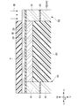
- FIG. 3 is a cross-sectional view of the domain wall moving element 101 according to the first embodiment.
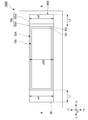
- FIG. 4 is a plan view of the domain wall moving element 101 according to the first embodiment.
- the domain wall moving element 101 has a first ferromagnetic layer 10, a magnetic recording layer 20, a non-magnetic layer 30, a first conductive portion 40, and a second conductive portion 50.
- FIG. 3 is a cross-sectional view of the domain wall moving element 101 cut along the xz plane (plane AA in FIG. 4) passing through the center of the magnetic recording layer 20 in the y direction.
- the domain wall moving element 101 is used as a storage element as an example.
- the first ferromagnetic layer 10 faces the non-magnetic layer 30.
- the first ferromagnetic layer 10 has a magnetization M 10 oriented in one direction. Magnetization M 10 of the first ferromagnetic layer 10, the orientation direction than the magnetization of the magnetic recording layer 20 is hardly changed when a predetermined external force is applied.
- the predetermined external force is, for example, an external force applied to the magnetization by an external magnetic field or an external force applied to the magnetization by a spin polarization current.
- the first ferromagnetic layer 10 is sometimes called a magnetization fixed layer or a magnetization reference layer. Magnetization M 10 is oriented in the z direction, for example.
- the magnetization of the magnetic recording layer 20 and the first ferromagnetic layer 10 may be oriented in any direction in the xy plane.
- the magnetization is oriented in the z direction
- the power consumption of the domain wall moving element 101 and the heat generation during operation are suppressed as compared with the case where the magnetization is oriented in the xy plane.
- the movement width of the domain wall 27 when a pulse current of the same intensity is applied is smaller than that when the magnetization is oriented in the xy plane.
- the change width (MR ratio) of the magnetic resistance of the domain wall moving element 101 is larger than that when the magnetization is oriented in the z direction.
- the first ferromagnetic layer 10 contains a ferromagnet.
- the ferromagnetic material constituting the first ferromagnetic layer 10 include a metal selected from the group consisting of Cr, Mn, Co, Fe and Ni, an alloy containing one or more of these metals, and these metals and B. , C, and N can be used as an alloy containing at least one or more elements.
- the first ferromagnetic layer 10 is, for example, Co—Fe, Co—Fe—B, Ni—Fe.
- the material constituting the first ferromagnetic layer 10 may be a Whistler alloy.
- the Whisler alloy is a half metal and has a high spin polarizability.
- the Whisler alloy is an intermetallic compound having a chemical composition of XYZ or X 2 YZ, where X is a transition metal element or noble metal element of the Co, Fe, Ni or Cu group on the periodic table, and Y is Mn, V. , Cr or Ti group transition metal or X elemental species, Z is a typical element of groups III to V.
- Examples of the Whisler alloy include Co 2 FeSi, Co 2 FeGe, Co 2 FeGa, Co 2 MnSi, Co 2 Mn 1-a Fe a Al b Si 1-b , and Co 2 FeGe 1-c Ga c .
- the film thickness of the first ferromagnetic layer 10 is preferably 1.5 nm or less, preferably 1.0 nm or less, when the easy axis of magnetization of the first ferromagnetic layer 10 is in the z direction (perpendicular magnetization film). Is more preferable.
- the first ferromagnetic layer 10 is perpendicularly magnetically anisotropic (interfacial vertical magnetism) at the interface between the first ferromagnetic layer 10 and another layer (non-magnetic layer 30). Anisotropy) is added, and the magnetization of the first ferromagnetic layer 10 is easily oriented in the z direction.
- the first ferromagnetic layer 10 is a ferromagnet selected from the group consisting of Co, Fe, and Ni, and Pt It is preferable to form a laminate with a non-magnetic material selected from the group consisting of Pd, Ru, and Rh, and an intermediate layer selected from the group consisting of Ir and Ru may be inserted at any position of the laminate. More preferred. Vertical magnetic anisotropy can be added by laminating a ferromagnetic material and a non-magnetic material, and by inserting an intermediate layer, the magnetization of the first ferromagnetic layer 10 can be easily oriented in the z direction.
- Magnetic recording layer The magnetic recording layer 20 extends in the x direction.
- the magnetic recording layer 20 is an example of a second ferromagnetic layer.
- the magnetic recording layer 20 is, for example, a rectangle having a major axis in the x direction and a minor axis in the y direction in a plan view from the z direction.
- the magnetic recording layer 20 is a magnetic layer facing the first ferromagnetic layer 10 with the non-magnetic layer 30 interposed therebetween.
- the magnetic recording layer 20 connects between the first conductive portion 40 and the second conductive portion 50.
- the magnetic recording layer 20 is a layer capable of magnetically recording information by changing the internal magnetic state.
- the magnetic recording layer 20 has a first magnetic domain 28 and a second magnetic domain 29 inside.
- the boundary between the first magnetic domain 28 and the second magnetic domain 29 is the domain wall 27.
- the magnetic recording layer 20 can have a magnetic domain wall 27 inside.
- Magnetic recording layer 20 shown in FIG. 3, the magnetization M 28 of the first magnetic domain 28 is oriented in the + z-direction, the magnetization M 29 of the second magnetic domain 29 is oriented in the -z direction.
- the domain wall moving element 101 can record data in multiple values or continuously depending on the position of the domain wall 27 of the magnetic recording layer 20.
- the data recorded on the magnetic recording layer 20 is read out as a change in the resistance value of the domain wall moving element 101 when a read-out current is applied.
- the ratio of the first magnetic domain 28 to the second magnetic domain 29 in the magnetic recording layer 20 changes as the domain wall 27 moves.
- Magnetization M 10 of the first ferromagnetic layer 10 is, for example, the same direction as the magnetization M 28 of the first magnetic domain 28 (parallel), in the opposite direction to the magnetization M 29 of the second magnetic domain 29 (antiparallel).
- the domain wall 27 moves in the + x direction and the area of the first magnetic domain 28 in the portion overlapping with the first ferromagnetic layer 10 in a plan view from the z direction becomes large, the resistance value of the domain wall moving element 101 becomes low.
- the domain wall 27 moves by passing a writing current in the x direction of the magnetic recording layer 20 or applying an external magnetic field. For example, when a write current (for example, a current pulse) is applied in the + x direction of the magnetic recording layer 20, electrons flow in the ⁇ x direction opposite to the current, and the domain wall 27 moves in the ⁇ x direction.
- a current flows from the first magnetic domain 28 to the second magnetic domain 29, the spin-polarized electrons in the second magnetic domain 29 reverse the magnetization M 28 of the first magnetic domain 28.
- magnetization M 28 of the first magnetic domain 28 to the magnetization reversal the domain wall 27 moves in the -x direction.
- the magnetic recording layer 20 is made of a magnetic material.
- the magnetic material constituting the magnetic recording layer 20 is a metal selected from the group consisting of Cr, Mn, Co, Fe and Ni, an alloy containing one or more of these metals, and B, C, and N of these metals.
- An alloy or the like containing at least one kind of element can be used. Specific examples thereof include Co-Fe, Co-Fe-B, and Ni-Fe.
- the magnetic recording layer 20 preferably has at least one element selected from the group consisting of Co, Ni, Pt, Pd, Gd, Tb, Mn, Ge, and Ga.
- the magnetic recording layer 20 may be, for example, a laminated film of Co and Ni, a laminated film of Co and Pt, or a laminated film of Co and Pd.
- the magnetic recording layer 20 may contain, for example, a MnGa-based material, a GdCo-based material, or a TbCo-based material.
- Ferrimagnetic materials such as MnGa-based materials, GdCo-based materials, and TbCo-based materials have a small saturation magnetization, and the magnetic recording layer 20 containing these materials has a small threshold current required to move the domain wall.
- the Co and Ni laminated film, the Co and Pt laminated film, and the Co and Pd laminated film have a large coercive force, and the magnetic recording layer 20 including these laminated films slows down the moving speed of the domain wall.
- the magnetic recording layer 20 may have a configuration (synthetic ferri configuration) in which a plurality of ferromagnetic layers are antiferromagnetically coupled with an intermediate layer interposed therebetween.
- the intermediate layer is, for example, Ru
- the plurality of ferromagnetic layers are, for example, a laminated film of CoFe and Pd.
- Non-magnetic layer The non-magnetic layer 30 is located between the first ferromagnetic layer 10 and the magnetic recording layer 20. The non-magnetic layer 30 is laminated on one surface of the magnetic recording layer 20.
- the non-magnetic layer 30 is made of, for example, a non-magnetic insulator, a semiconductor or a metal.
- the non-magnetic insulator is, for example, Al 2 O 3 , SiO 2 , MgO, MgAl 2 O 4 , and a material in which some of these Al, Si, and Mg are replaced with Zn, Be, and the like. These materials have a large bandgap and are excellent in insulating properties.
- the non-magnetic layer 30 is made of a non-magnetic insulator, the non-magnetic layer 30 is a tunnel barrier layer.
- Non-magnetic metals are, for example, Cu, Au, Ag and the like.
- Non-magnetic semiconductors are, for example, Si, Ge, CuInSe 2 , CuGaSe 2 , Cu (In, Ga) Se 2, and the like.
- the thickness of the non-magnetic layer 30 is preferably 20 ⁇ or more, and more preferably 30 ⁇ or more.
- the resistance area product (RA) of the domain wall moving element 101 becomes large.
- the resistance area product (RA) of the domain wall moving element 101 is preferably 1 ⁇ 10 5 ⁇ ⁇ m 2 or more, and more preferably 1 ⁇ 10 6 ⁇ ⁇ m 2 or more.
- the resistance area product (RA) of the domain wall moving element 101 is the product of the element resistance of one domain wall moving element 101 and the element cross-sectional area of the domain wall moving element 101 (the area of the cut surface obtained by cutting the non-magnetic layer 30 in the xy plane). expressed.
- the first conductive portion 40 and the second conductive portion 50 sandwich at least a part of the magnetic recording layer 20 in the x direction.
- the first conductive portion 40 and the second conductive portion 50 are separated from each other and connected to the magnetic recording layer 20.
- the first conductive portion 40 and the second conductive portion 50 are connected to, for example, the connection wiring Cw (see FIG. 2).
- Each of the first conductive portion 40 and the second conductive portion 50 may be a part of the connection wiring Cw, for example.
- the first conductive portion 40 is connected to, for example, the first end portion of the magnetic recording layer 20, and the second conductive portion 50 is connected to, for example, the second end portion of the magnetic recording layer 20.
- the plan view shape of the first conductive portion 40 and the second conductive portion 50 when viewed from the z direction is not particularly limited.
- the first conductive portion 40 and the second conductive portion 50 shown in FIG. 4 are rectangular in a plan view from the z direction.
- the first conductive portion 40 and the second conductive portion 50 may be circular or elliptical.
- the widths w1 and w2 of the first conductive portion 40 and the second conductive portion 50 in the y direction are wider than, for example, the width w20 of the magnetic recording layer 20 in the y direction.
- the first conductive portion 40 has a first magnetic layer 41, a second magnetic layer 42, and a first intermediate layer 43.
- the first conductive portion 40 has a first magnetic layer 41, a first intermediate layer 43, and a second magnetic layer 42 in order from the side closer to the magnetic recording layer 20.
- the first magnetic layer 41 is in contact with the magnetic recording layer 20.
- the first magnetic layer 41 and the second magnetic layer 42 include a ferromagnet.
- the first magnetic layer 41 and the second magnetic layer 42 include, for example, the same materials as those applied to the first ferromagnetic layer 10 and the magnetic recording layer 20.
- the first magnetic layer 41 and the second magnetic layer 42 may be, for example, a single layer composed of a single material or a plurality of layers.
- FIG. 3 illustrates a case where the first magnetic layer 41 and the second magnetic layer 42 are a single layer.
- the magnetization M 41 of the first magnetic layer 41 and the magnetization M 42 of the second magnetic layer 42 aligned in different directions.
- Magnetization M 41 of the first magnetic layer 41 is, for example, + z and oriented in the direction
- the magnetization M 42 of the second magnetic layer 42 are oriented for example in the -z direction.
- the + z direction is an example of the first magnetization direction
- the ⁇ z direction is an example of the second magnetization direction.
- the first intermediate layer 43 is a layer that magnetically couples two ferromagnets.
- the first intermediate layer 43 may be referred to as a magnetic coupling layer or an insertion layer.
- the first intermediate layer 43 is made of a non-magnetic material.
- the first intermediate layer 43 includes, for example, at least one selected from the group consisting of Ru, Ir, and Rh.
- the thickness of the first intermediate layer 43 is, for example, 2 nm or less, preferably 1 nm or less.
- the first intermediate layer 43 is sandwiched between two magnetization regions (first magnetization region A1 and second magnetization region A2).
- first magnetization region A1 coincides with the first magnetic layer 41
- the second magnetization region A2 coincides with the second magnetic layer 42.
- the first magnetization region A1 and the second magnetization region A2 are antiferromagnetically coupled via, for example, the first intermediate layer 43.
- the second conductive portion 50 has a third magnetic layer 51, a fourth magnetic layer 52, and a second intermediate layer 53.
- the second conductive portion 50 has a third magnetic layer 51, a second intermediate layer 53, and a fourth magnetic layer 52 in order from the side closer to the magnetic recording layer 20.
- the third magnetic layer 51 is in contact with the magnetic recording layer 20.
- the third magnetic layer 51 and the fourth magnetic layer 52 include a ferromagnet.
- the third magnetic layer 51 and the fourth magnetic layer 52 include, for example, the same materials as those applied to the first ferromagnetic layer 10 and the magnetic recording layer 20.
- the third magnetic layer 51 and the fourth magnetic layer 52 may be, for example, a single layer composed of a single material or a plurality of layers.
- FIG. 3 illustrates a case where the third magnetic layer 51 and the fourth magnetic layer 52 are a single layer. Magnetization M 51 of the third magnetic layer 51 are oriented for example in a direction different from the magnetization M 41, M 52 of the first magnetic layer 41 and fourth magnetic layer 52.
- Magnetization M 51 of the third magnetic layer 51 are oriented for example in the same direction as the magnetization M 42 of the second magnetic layer 42.
- Magnetization M 52 of the fourth magnetic layer 52 are oriented for example in a direction different from the magnetization M 42, M 51 of the second magnetic layer 42 and the third magnetic layer 51.
- Magnetization M 52 of the fourth magnetic layer 52 are oriented for example in the same direction as the magnetization M 41 of the first magnetic layer 41.
- Magnetization M 51 of the third magnetic layer 51 for example oriented in the -z direction
- the magnetization M 52 of the fourth magnetic layer 52 is oriented in the example the + z direction.
- the second intermediate layer 53 is a layer that magnetically couples two ferromagnets.
- the second intermediate layer 53 may be referred to as a magnetic coupling layer or an insertion layer.
- the material and thickness of the second intermediate layer 53 are the same as those of the first intermediate layer 43.
- the second intermediate layer 53 is sandwiched between two magnetization regions (third magnetization region A3 and fourth magnetization region A4).
- the third magnetization region A3 coincides with the third magnetic layer 51
- the fourth magnetization region A4 coincides with the fourth magnetic layer 52.
- the third magnetization region A3 and the fourth magnetization region A4 are antiferromagneticly coupled via, for example, a second intermediate layer 53.
- the thickness h1 of the first magnetization region A1 in the z direction is thicker than the thickness h2 of the second magnetization region A2 in the z direction.
- the length L1 of the first conductive portion 40 in the x direction is substantially constant at each position in the z direction. Approximately constant means that the amount of change with respect to the average value is 10% or less. Therefore, the difference between the thicknesses h1 and h2 can be converted into an area, and the area of the first magnetization region A1 is larger than the area of the second magnetization region A2. Further, the width w1 of the first conductive portion 40 in the y direction (see FIG. 4) is also substantially constant at each position in the x direction. Therefore, the difference between the thicknesses h1 and h2 can be converted into a volume.
- the thickness h3 of the third magnetization region A3 in the z direction is thinner than the thickness h4 of the fourth magnetization region A4 in the z direction.
- the length L2 in the x direction and the width w2 in the y direction of the second conductive portion 50 are substantially constant.
- the difference between the thicknesses h3 and h4 can be converted into area and volume.
- the area of the third magnetization region A3 is smaller than the area of the fourth magnetization region A4.
- the thickness h2 of the second magnetization region A2 and the thickness h4 of the fourth magnetization region A4 are, for example, equal.
- equality is not limited to the case where they are exactly the same, and an error of about 10% is allowed. That is, the thickness h2 of the second magnetization region A2 and the thickness h4 of the fourth magnetization region A4 are, for example, equal. ..
- the area of the second magnetization region A2 and the area of the fourth magnetization region A4 are, for example, equal (substantially the same).
- the first intermediate layer 43 and the second intermediate layer 53 are laminated on the second magnetization region A2 and the fourth magnetization region A4, respectively.
- the first intermediate layer 43 and the second intermediate layer 53 are, for example, at the same height position in the z direction. By aligning the height positions of the first intermediate layer 43 and the second intermediate layer 53 in the z direction, the first intermediate layer 43 and the second intermediate layer 53 can be formed at one time.
- the thickness h1 of the first magnetization region A1 is thicker than, for example, the thickness h3 of the third magnetization region A3.
- the area of the first magnetization region A1 is larger than the area of the third magnetization region A3, for example.
- the thicknesses h1 and h3 of the first magnetization region A1 and the third magnetization region A3 are thicker than, for example, the thickness h20 of the magnetic recording layer 20. Further, the widths w1 and w2 of the first magnetization region A1 and the third magnetization region A3 in the y direction are wider than, for example, the width w20 of the magnetic recording layer 20 in the y direction.
- the area of the cross section obtained by cutting the first magnetization region A1 and the third magnetization region A3 in the yz plane is, for example, the area of the cross section obtained by cutting the magnetic recording layer 20 in the yz plane (h20 ⁇ w20). ) Greater. Since the current density in the first magnetization region A1 and the third magnetization region A3 is larger than the current density in the magnetic recording layer 20, the invasion of the domain wall 27 into the first magnetization region A1 and the third magnetization region A3 can be further suppressed.
- the magnetization directions of the first ferromagnetic layer 10, the magnetic recording layer 20, the first conductive portion 40, and the second conductive portion 50 of the domain wall moving element 100 can be confirmed, for example, by measuring the magnetization curve.
- the magnetization curve can be measured using, for example, MOKE (Magneto Optical Kerr Effect).
- MOKE Magnetic Optical Kerr Effect
- the measurement by MOKE is a measurement method performed by making linearly polarized light incident on an object to be measured and using a magneto-optical effect (magnetic Kerr effect) in which rotation in the polarization direction occurs.
- the manufacturing method of the magnetic recording array 200 will be described.
- the magnetic recording array 200 is formed by a laminating step of each layer and a processing step of processing a part of each layer into a predetermined shape.
- a sputtering method, a chemical vapor deposition (CVD) method, an electron beam vapor deposition method (EB vapor deposition method), an atomic laser deposit method, or the like can be used.
- the processing of each layer can be performed using photolithography, ion milling, or the like.
- impurities are doped at a predetermined position on the substrate Sub to form a source region S and a drain region D.
- a gate insulating film GI and a gate electrode G are formed between the source region S and the drain region D.
- the source region S, the drain region D, the gate insulating film GI, and the gate electrode G serve as a transistor Tr.
- the insulating layer 60 is formed so as to cover the transistor Tr. Further, the connection wiring Cw is formed by forming an opening in the insulating layer 60 and filling the opening with a conductor.
- the first wiring Cm, the second wiring Wp, and the third wiring Rp are formed by laminating the insulating layer 60 to a predetermined thickness, forming a groove in the insulating layer 60, and filling the groove with a conductor.
- Each layer constituting the first conductive portion 40 and the second conductive portion 50 may form an opening in the insulating layer 60 and may be laminated in order in the opening. Further, after laminating the layers constituting the first conductive portion 40 and the second conductive portion 50, only the portions to be the first conductive portion 40 and the second conductive portion 50 may be removed.
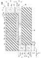
- FIG. 5 is a cross-sectional view showing a part of the first manufacturing method of the domain wall moving element 101.
- the first conductive portion 40, the second conductive portion 50, and the magnetic recording layer 20 are formed inside the insulating layer 60.
- the magnetic recording layer 20 is formed on, for example, one surface of the insulating layer 60 by a sputtering method.
- the surfaces of the first conductive portion 40 and the magnetic recording layer 20 are covered with the protective film P.
- the protective film P is, for example, a resist.
- the laminated film is irradiated with an ion beam IB.
- the first conductive portion 40 and the magnetic recording layer 20 protected by the protective film P are not removed by the ion beam IB, but a part of the third magnetic layer 51 of the second conductive portion 50 is removed by the ion beam IB.
- the thickness h3 of the third magnetic layer 51 is thinner than the thickness h1 of the first magnetic layer 41.
- the non-magnetic layer and the ferromagnetic layer are laminated in this order at positions overlapping the magnetic recording layer 20 in the z direction and processed into a predetermined shape to form the non-magnetic layer 30 and the first ferromagnetic layer 10.
- the domain wall moving element 101 can be manufactured by such a procedure.
- FIG. 6 is a cross-sectional view showing a part of the second manufacturing method of the domain wall moving element 101.
- the non-magnetic layer 30 and the first ferromagnetic layer 10 may be laminated and then irradiated with an ion beam IB.
- the processing of the non-magnetic layer 30 and the first ferromagnetic layer 10 and the processing of the third magnetic layer 51 can be performed at the same time.
- the domain wall moving element 101 can easily define the initial state only by applying an external magnetic field in one direction.
- the initial state includes both the initial state before shipment and the initial state after refreshing the data in the usage process.
- the provision of the initial state before shipment is particularly useful for improving the yield.
- a large magnetic field is applied to the domain wall moving element 101 in the + z direction.
- all the magnetizations M 10 , M 28 , M 29 , M 41 , M 42 , M 51 , and M 52 constituting the domain wall moving element 101 are oriented in the + z direction.
- the magnetization M 41 and the magnetization M 42 try to be oriented in opposite directions. This is because the first magnetic layer 41 and the second magnetic layer 42 are antiferromagnetically coupled via the first intermediate layer 43.
- the magnetization M 51 and the magnetization M 52 try to be oriented in opposite directions. This is because the third magnetic layer 51 and the fourth magnetic layer 52 are antiferromagnetically coupled via the second intermediate layer 53.
- the first magnetic layer 41 is thicker than the second magnetic layer 42, and the first magnetic layer 41 has a larger coercive energy than the second magnetic layer 42.
- the coercive energy is energy proportional to the product of saturation magnetization and thickness (area). The larger the coercive energy, the more difficult it is for magnetization reversal. Magnetization M 41 of the first magnetic layer 41 maintains the orientation of the + z-direction, the magnetization M 42 of the second magnetic layer 42 is oriented in the -z direction.
- the third magnetic layer 51 is thinner than the fourth magnetic layer 52, and the third magnetic layer 51 has a smaller coercive energy than the fourth magnetic layer 52.
- Magnetization M 52 of the fourth magnetic layer 52 maintains the orientation of the + z-direction, the magnetization M 51 of the third magnetic layer 51 is oriented in the -z direction.
- the orientation directions of the magnetizations M 41 and M 51 of the first magnetic layer 41 and the third magnetic layer 51, which are in contact with the magnetic recording layer 20, are different from each other.
- a magnetic domain wall 27 is formed inside the magnetic recording layer 20 in order to eliminate the difference in the orientation direction. That is, by simply applying an external magnetic field in one direction, different magnetization states can be formed at both ends of the magnetic recording layer 20, and the domain wall 27 can be generated inside. Since the domain wall 27 is formed at an arbitrary position, the initial state can be easily defined.
- domain wall moving element 101 according to the first embodiment can be variously modified and changed within the scope of the gist of the present invention.
- FIG. 7 is a cross-sectional view of the domain wall moving element 101A according to the first modification.
- the domain wall moving element 101A shown in FIG. 7 is different from the domain wall moving element 101 shown in FIG. 3 in that the first magnetic layer 41 and the third magnetic layer 51 have a two-layer structure.
- Other configurations are the same as those of the domain wall moving element 101, and the same reference numerals are given to the same configurations, and the description thereof will be omitted.
- the first magnetic layer 41 has a first layer 411 and a second layer 412.
- the first layer 411 is made of the same material as the magnetic recording layer 20. There is no boundary between the first layer 411 and the magnetic recording layer 20, and the portion overlapping the first intermediate layer 43 in the z direction is the first layer 411.
- the second layer 412 is made of a material different from that of the first layer 411.
- the first layer 411 and the second layer 412 are magnetically bonded to each other.
- the region where the first layer 411 and the second layer 412 are combined is the first magnetization region A1.
- the third magnetic layer 51 has a first layer 511 and a second layer 512.
- the first layer 511 is made of the same material as the magnetic recording layer 20. There is no boundary between the first layer 511 and the magnetic recording layer 20, and the portion overlapping the second intermediate layer 53 in the z direction is the first layer 511.
- the second layer 512 is made of a material different from that of the first layer 511.
- the first layer 511 and the second layer 512 are magnetically bonded to each other.
- the region where the first layer 511 and the second layer 512 are combined is the third magnetization region A3.
- the domain wall moving element 101A is obtained by forming a second layer 412, 512 and an insulating layer 60, and then forming a magnetic layer on them. A part of the formed magnetic layer becomes the first layer 411, 511 and the magnetic recording layer 20, respectively.
- the first magnetization region A1 has a larger coercive energy than the second magnetization region A2, and the third magnetization region A3 has a smaller coercive energy than the fourth magnetization region A4. It has the same effect as the domain wall moving element 101 according to the first embodiment.
- FIG. 8 is a cross-sectional view of the domain wall moving element 102A according to the second embodiment.
- FIG. 8 is a cross-sectional view of the domain wall moving element 102A cut along the xz plane (plane AA in FIG. 9) passing through the center of the magnetic recording layer 20 in the y direction.
- FIG. 9 is a plan view of the domain wall moving element 102A according to the second embodiment.
- the domain wall moving element 102A is different from the domain wall moving element 101 according to the first embodiment in the shapes of the first ferromagnetic layer 10A, the non-magnetic layer 30A, the magnetic recording layer 20A, and the second conductive portion 50A.
- Other configurations are the same as those of the domain wall moving element 101, and the same reference numerals are given to the same configurations, and the description thereof will be omitted.
- the side surfaces 10s and 30s in the x direction are inclined in the x direction with respect to the xy plane.
- the width of the first ferromagnetic layer 10A and the non-magnetic layer 30A increases in the x direction as it approaches the magnetic recording layer 20.
- the first ferromagnetic layer 10A and the non-magnetic layer 30A also have side surfaces 10s and 30s in the y direction inclined in the y direction with respect to the xy plane.
- the side surface 10s and the side surface 30s are continuous with each other. "Continuous" means that the inclination angle of the tangent does not change stepwise, and includes the case where the inclination angle of the tangent is constant and the case where the inclination angle of the tangent changes continuously.
- the magnetic recording layer 20A is different from the magnetic recording layer 20 according to the first embodiment in that the magnetic recording layer 20A has an inclined surface 20s at the end on the second conductive portion 50A side.
- the inclined surface 20s is inclined in the x direction with respect to the xy plane.
- the inclined surface 20s is discontinuous with the side surfaces 10s and 30s. There is a step between the side surface 30s and the inclined surface 20s.
- the shape of the third magnetic layer 51A of the second conductive portion 50A is different from that of the second conductive portion 50 according to the first embodiment.
- the area of the third magnetic layer 51A in FIG. 8 is smaller than the area of the fourth magnetic layer 52. Therefore, the area of the third magnetization region A3 is smaller than that of the fourth magnetization region A4. Further, the third magnetic layer 51A has a portion thinner than the fourth magnetic layer 52.
- the first surface 50a of the third magnetic layer 51A is inclined in the x direction with respect to the xy plane.
- the first surface 50a is a surface of the third magnetic layer 51A on the side closer to the first ferromagnetic layer 10A in the z direction, and is opposite to the surface in contact with the second intermediate layer 53 of the third magnetization region A3 in the z direction. is there.
- the first surface 50a is continuous with the inclined surface 20s.
- the domain wall moving element 102A is likely to be formed when the second conductive portion 50A, the first ferromagnetic layer 10A, and the non-magnetic layer 30A are processed separately (when the manufacturing conditions shown in FIG. 5 are adopted).
- the first magnetization region A1 has a larger coercive energy than the second magnetization region A2, and the third magnetization region A3 has a smaller coercive energy than the fourth magnetization region A4. It has the same effect as the domain wall moving element 101 according to the first embodiment. Further, the first surface 50a and the inclined surface 20s make the current flow from the second conductive portion 50A to the magnetic recording layer 20 smooth, and energy loss can be suppressed.
- FIG. 10 is a cross-sectional view of the domain wall moving element 102B according to the second modification.
- FIG. 11 is a plan view of the domain wall moving element 102B according to the second modification.
- the domain wall moving element 102B is different from the domain wall moving element 102A in the shapes of the magnetic recording layer 20 and the second conductive portion 50B.
- the same components as those of the domain wall moving element 102A are designated by the same reference numerals, and the description thereof will be omitted.
- the magnetic recording layer 20 is the same as the magnetic recording layer 20 according to the first embodiment.
- the shape of the third magnetic layer 51B of the second conductive portion 50B is different from that of the second conductive portion 50 according to the first embodiment.
- the area of the third magnetic layer 51B in FIG. 10 is smaller than the area of the fourth magnetic layer 52. Therefore, the area of the third magnetization region A3 is smaller than that of the fourth magnetization region A4. Further, the third magnetic layer 51B has a portion thinner than the fourth magnetic layer 52.
- the first surface 50b of the third magnetic layer 51B is composed of a flat surface 50b1 and an inclined surface 50b2.
- the flat surface 50b1 is parallel to the xy plane.
- the inclined surface 50b2 is inclined in the x direction with respect to the xy plane.
- the domain wall moving element 102B is likely to be formed when the second conductive portion 50B, the first ferromagnetic layer 10A, and the non-magnetic layer 30A are processed separately (when the manufacturing conditions shown in FIG. 5 are adopted).
- the domain wall moving element 102B according to the second modification has the same effect as the domain wall moving element 102A. Since the inclined surface 20s is not formed on the magnetic recording layer 20, the fluctuation of the current density in the magnetic recording layer 20 can be reduced. The moving conditions of the domain wall 27 change as the current density changes. When the fluctuation of the current density in the magnetic recording layer 20 is small, the operation of the domain wall 27 is stabilized.
- FIG. 12 is a cross-sectional view of the domain wall moving element 102C according to the third modification.
- FIG. 13 is a plan view of the domain wall moving element 102C according to the third modification.
- the domain wall moving element 102C is different from the domain wall moving element 102A in that the side surfaces 10s and 30s, the inclined surface 20s, and the first surface 50a are continuous.
- the same components as those of the domain wall moving element 102A are designated by the same reference numerals, and the description thereof will be omitted.
- the side surfaces 10s and 30s, the inclined surface 20s, and the first surface 50a are continuous.
- the domain wall moving element 102C has no step between the side surface 30s and the inclined surface 20s.
- the domain wall moving element 102C is likely to be formed when the second conductive portion 50A, the first ferromagnetic layer 10A, and the non-magnetic layer 30A are processed at the same time (when the manufacturing conditions shown in FIG. 6 are adopted).
- the manufacturing process is simplified.
- the width w2 of the second conductive portion 50A in the y direction and the magnetic recording layer 20 The width w20 in the y direction is substantially the same.
- the domain wall moving element 102C according to the third modification has the same effect as the domain wall moving element 102A.
- FIG. 14 is a cross-sectional view of the domain wall moving element 102D according to the fourth modification.
- FIG. 15 is a plan view of the domain wall moving element 102D according to the fourth modification.
- the domain wall moving element 102D is different from the domain wall moving element 102B in that the first ferromagnetic layer 10A and the non-magnetic layer 30A overlap with the second conductive portion 50B.
- the same components as those of the domain wall moving element 102B are designated by the same reference numerals, and the description thereof will be omitted.
- the first ferromagnetic layer 10A and the non-magnetic layer 30A project from the magnetic recording layer 20 in the + x direction.
- the magnetic recording layer 20 is hidden by the first ferromagnetic layer 10A and the non-magnetic layer 30A in a plan view from the + z direction.
- a part of the non-magnetic layer 30A is in contact with the flat surface 50b1 of the second conductive portion 50B.
- the side surfaces 10s and 30s and the inclined surface 50b2 are continuous.
- the domain wall moving element 102D is likely to be formed when the second conductive portion 50B, the first ferromagnetic layer 10A, and the non-magnetic layer 30A are processed at the same time (when the manufacturing conditions shown in FIG. 6 are adopted).
- the manufacturing process is simplified.
- the width w2 of the second conductive portion 50B in the y direction and the width w20 of the magnetic recording layer 20 in the y direction Is almost the same.
- the domain wall moving element 102D according to the fourth modification has the same effect as the domain wall moving element 102B.
- FIG. 16 is a cross-sectional view of the domain wall moving element 102E according to the fifth modification.
- FIG. 17 is a plan view of the domain wall moving element 102E according to the fifth modification.
- the shape of the second conductive portion 50E of the domain wall moving element 102E is different from that of the domain wall moving element 102A.
- the same components as those of the domain wall moving element 102A are designated by the same reference numerals, and the description thereof will be omitted.
- the second conductive portion 50E is different from the domain wall moving element 102A in that the length L2'in the x direction is longer than the length L1 in the x direction of the first conductive portion 40.
- the inclination angle of the first surface 50a with respect to the xy plane becomes gentle. For example, even if the same thickness is cut by ion milling, the length in the x direction becomes longer.
- FIG. 18 is a cross-sectional view of the domain wall moving element 103A according to the third embodiment.
- FIG. 18 is a cross-sectional view of the domain wall moving element 103A cut along the xz plane passing through the center of the magnetic recording layer 20 in the y direction.
- the structure of the second conductive portion 55 of the domain wall moving element 103A is different from that of the domain wall moving element 101 shown in FIG.
- the same components as those of the domain wall moving element 101 are designated by the same reference numerals, and the description thereof will be omitted.
- the second conductive portion 55 has a third magnetic layer 51, a fourth magnetic layer 52, and a second intermediate layer 53.
- the first surface 55a of the second conductive portion 55 is at the same height as the first surface 20a of the magnetic recording layer 20.
- the first surface 55a and the first surface 20a form a flat surface.
- the thickness h1 of the first magnetization region A1 and the thickness h3 of the third magnetization region A3 are, for example, the same (substantially the same).
- the area of the first magnetization region A1 and the area of the third magnetization region A3 are, for example, the same (substantially the same).
- the thickness h2 of the second magnetization region A2 is thinner than the thickness h4 of the fourth magnetization region A4.
- the area of the second magnetization region A2 is smaller than the area of the fourth magnetization region A4.
- the first magnetization region A1 has a larger coercive energy than the second magnetization region A2, and the third magnetization region A3 has a smaller coercive energy than the fourth magnetization region A4. It has the same effect as the domain wall moving element 101 according to the first embodiment.
- FIG. 19 is a cross-sectional view of the domain wall moving element 103B according to the sixth modification.
- the domain wall moving element 103B shown in FIG. 19 is different from the domain wall moving element 103A shown in FIG. 18 in that the second conductive portion 56 extends in the + z direction.
- the same components as those of the domain wall moving element 103A are designated by the same reference numerals, and the description thereof will be omitted.
- the directions in which the first conductive portion 40 and the second conductive portion 56 extend may be different.
- the first conductive portion 40 and the second conductive portion 56 extend in different directions with respect to the magnetic recording layer 20.
- the semiconductor device is formed for each layer.
- the first conductive portion 40 and the second conductive portion 56 may extend in different directions due to the wiring and the like.
- the distance L3 between the second conductive portion 56 and the first ferromagnetic layer 10 in the x direction is longer than, for example, the distance L4 between the first conductive portion 40 and the first ferromagnetic layer 10 in the x direction.
- the second conductive portion 56 is a conductive portion that extends in the same direction as the direction in which the first ferromagnetic layer 10 is laminated with reference to the magnetic recording layer 20.
- the first conductive portion 40 is a conductive portion that extends in a direction opposite to the direction in which the first ferromagnetic layer 10 is laminated with reference to the magnetic recording layer 20.
- FIG. 20 is a cross-sectional view of the domain wall moving element 104 according to the fourth embodiment.
- FIG. 20 is a cross-sectional view of the domain wall moving element 104 cut along the xz plane passing through the center of the magnetic recording layer 20 in the y direction.
- the domain wall moving element 104 is different from the domain wall moving element 101 shown in FIG. 3 in that the configuration of the first ferromagnetic layer 15 and the third ferromagnetic layer 70 are provided. The description of the same configuration as that of the domain wall moving element 101 will be omitted.
- the third ferromagnetic layer 70 is located between the magnetic recording layer 20 and the non-magnetic layer 30.
- the third ferromagnetic layer 70 contains a magnetic material.
- the third ferromagnetic layer 70 reflects the magnetic state of the magnetic recording layer 20.
- the magnetic material constituting the third ferromagnetic layer 70 the same magnetic material as that of the first ferromagnetic layer 10 according to the first embodiment can be used.
- the third ferromagnetic layer 70 is adjacent to the magnetic recording layer 20.
- An intermediate layer may be provided between the third ferromagnetic layer 70 and the magnetic recording layer 20.
- the intermediate layer is, for example, Ru.
- the magnetizations M 78 and M 79 of the third ferromagnetic layer 70 are magnetically coupled to the magnetizations M 28 and M 29 of the magnetic recording layer 20.
- the third ferromagnetic layer 70 reflects the magnetic state of the magnetic recording layer 20.
- the magnetic state of the third ferromagnetic layer 70 becomes the same as the magnetic state of the magnetic recording layer 20.
- the magnetic state of the third ferromagnetic layer 70 is opposite to the magnetic state of the magnetic recording layer 20.
- a first magnetic domain 78 and a second magnetic domain 79 are formed inside the third ferromagnetic layer 70.
- the change in magnetic resistance (MR ratio) of the domain wall moving element 104 is caused by a change in the magnetic state of two magnetic materials (fifth ferromagnetic layer 13 and third ferromagnetic layer 70) sandwiching the non-magnetic layer 30.
- the third ferromagnetic layer 70 preferably contains a material that easily obtains a coherent tunneling effect with the first ferromagnetic layer 10.
- the magnetic recording layer 20 preferably contains a material that slows down the moving speed of the domain wall 27.
- the first ferromagnetic layer 15 has a fourth ferromagnetic layer 11, a third intermediate layer 12, and a fifth ferromagnetic layer 13.
- the material constituting the fifth ferromagnetic layer 13 is the same as that of the first ferromagnetic layer 10 according to the first embodiment.
- the fourth ferromagnetic layer 11 may be made of the same material as the first ferromagnetic layer 10, and may contain IrMn, PtMn, or the like.
- the material constituting the third intermediate layer 12 is the same as that of the first intermediate layer 43.
- the first ferromagnetic layer 15 has a synthetic antiferromagnetic structure (SAF structure).
- the first magnetization region A1 has a larger coercive energy than the second magnetization region A2, and the third magnetization region A3 has a smaller coercive energy than the fourth magnetization region A4. It has the same effect as the domain wall moving element 101 according to the first embodiment. Further, since the first ferromagnetic layer 15 has a SAF structure, the coercive force of the fourth ferromagnetic layer 11 is large and the MR ratio is improved. Further, since the magnetic recording layer 20 is no longer two magnetic materials sandwiching the non-magnetic layer 30, the degree of freedom in selecting the material of the magnetic recording layer 20 is increased.
- FIG. 21 is a cross-sectional view of the domain wall moving element 104A according to the seventh modification.
- FIG. 20 shows that the domain wall moving element 104A shown in FIG. 21 extends to a position where the non-magnetic layer 31 and the third ferromagnetic layer 71 overlap the first conductive portion 40 and the second conductive portion 55 in the z direction. It is different from the domain wall moving element 104.
- the same components as those of the domain wall moving element 104 are designated by the same reference numerals, and the description thereof will be omitted.
- the third ferromagnetic layer 71 has a first superposed region 71A that overlaps the first conductive portion 40 in the z direction, and a second superposed region 71B that overlaps the second conductive portion 55 in the z direction.
- the first magnetization region A1 includes a first magnetic layer 41 and a first overlapping region 71A.
- the third magnetization region A3 includes a third magnetic layer 51 and a second superimposition region 71B.
- the domain wall moving element 104A according to the seventh modification also has the same effect as the domain wall moving element 104 according to the fourth embodiment.
- FIG. 22 is a cross-sectional view of the domain wall moving element 105 according to the fifth embodiment.
- FIG. 22 is a cross-sectional view of the domain wall moving element 105 cut along the xz plane passing through the center of the magnetic recording layer 20 in the y direction.
- the domain wall moving element 105 has a bottom pin structure in which the first ferromagnetic layer 10 is located closer to the substrate Sub than the magnetic recording layer 20.
- the same components as those in FIG. 20 are designated by the same reference numerals, and the description thereof will be omitted.
- the first intermediate layer 43 is sandwiched between the first magnetization region A1 and the second magnetization region A2 in the z direction.
- the portion of the third ferromagnetic layer 70 that overlaps the first magnetic layer 41 in the z direction is magnetically bonded to the first magnetic layer 41. Therefore, the first magnetization region A1 in the domain wall moving element 105 is a region in which the first magnetic layer 41, the first magnetic layer 41 of the third ferromagnetic layer 70, and the portion overlapping in the z direction are combined.
- the second magnetization region A2 coincides with the second magnetic layer 42.
- the second intermediate layer 53 is sandwiched between the third magnetization region A3 and the fourth magnetization region A4 in the z direction.
- the portion of the third ferromagnetic layer 70 that overlaps the third magnetic layer 51 in the z direction is magnetically bonded to the third magnetic layer 51. Therefore, the third magnetization region A3 in the domain wall moving element 105 is a region in which the third magnetic layer 51, the third magnetic layer 51 of the third ferromagnetic layer 70, and the portion overlapping in the z direction are combined.
- the fourth magnetization region A4 coincides with the fourth magnetic layer 52.
- the area of the first magnetization region A1 is larger than the area of the second magnetization region A2. Further, also in the domain wall moving element 105, the area of the third magnetization region A3 is smaller than the area of the fourth magnetization region A4.
- the thickness h1 of the first magnetization region A1 is thicker than the thickness h2 of the second magnetization region A2, and the thickness h3 of the third magnetization region A3 is thinner than the thickness h4 of the fourth magnetization region A4.
- the thickness difference between the thickness h2 of the second magnetization region A2 and the thickness h4 of the fourth magnetization region A4 is generated by, for example, milling the first conductive portion 40.
- the first magnetization region A1 has a larger coercive energy than the second magnetization region A2, and the third magnetization region A3 has a smaller coercive energy than the fourth magnetization region A4. It has the same effect as the domain wall moving element 101 according to the first embodiment.
- FIG. 23 is a modified example of the domain wall moving element according to the fifth embodiment. Even in the bottom pin structure as in the domain wall moving element 105A shown in FIG. 23, the direction in which the first conductive portion 40 extends and the direction in which the second conductive portion 50 extends may be different with respect to the magnetic recording layer 20.
- FIG. 24 is a cross-sectional view of the domain wall moving element 106 according to the sixth embodiment.
- FIG. 24 is a cross-sectional view of the domain wall moving element 106 cut along the xz plane passing through the center of the magnetic recording layer 20 in the y direction.
- the domain wall moving element 106 is different from the domain wall moving element 101 shown in FIG. 3 in that a part of the first conductive portion 40 protrudes from the magnetic recording layer 20 in the z direction.
- the description of the same configuration as that of the domain wall moving element 101 will be omitted.
- the first conductive portion 40 has a protruding portion PA protruding from the magnetic recording layer 20 in the z direction.
- the protruding portion PA belongs to the first magnetic layer 41 and belongs to the first magnetization region A1.
- the protruding portion PA projects from the magnetic recording layer 20 toward the side opposite to the side where the first conductive portion 40 extends with respect to the magnetic recording layer 20.
- the first conductive portion 40 refers to the magnetic recording layer 20.
- the protruding portion PA extends in the ⁇ z direction and projects in the + z direction with reference to the magnetic recording layer 20.
- a difference in thickness h1 and h3 between the first magnetic layer 41 and the third magnetic layer 51 was created by milling a part of each layer after laminating them.
- the difference in thickness h1 and h3 between the first magnetic layer 41 and the third magnetic layer 51 can be produced by additionally laminating the protruding portion PA after laminating each layer.
- the first magnetization region A1 has a larger coercive energy than the second magnetization region A2, and the third magnetization region A3 has a smaller coercive energy than the fourth magnetization region A4. It has the same effect as the domain wall moving element 101 according to the first embodiment.
- the characteristic configurations of the first to fifth embodiments may be combined. Further, the modification of each embodiment may be applied to other embodiments.
- Non-magnetic layer 40 1st conductive part 41 1st magnetic layer 42 2nd magnetic layer 43 1st intermediate layer 50, 50A, 50B, 50E, 55, 56 2nd conductive part 51, 51A, 51B 3rd magnetic layer 52 4th Magnetic layer 53 Second intermediate layer 60 Insulation layer 70, 71 Third ferromagnetic layer 71A First superimposition region 71B Second superimposition region 101, 101A, 102A, 102B, 102C, 102D, 102E, 103A, 103B, 104, 104A, 105, 105A, 106 Domain wall moving element 110 1st switching element 120 2nd switching element 130 3rd switching element 200 Magnetic recording array A1 1st magnetization region A2 2nd magnetization region A3 3rd
Landscapes
- Engineering & Computer Science (AREA)
- Computer Hardware Design (AREA)
- Hall/Mr Elements (AREA)
- Mram Or Spin Memory Techniques (AREA)
Priority Applications (3)
| Application Number | Priority Date | Filing Date | Title |
|---|---|---|---|
| JP2021519497A JP7173311B2 (ja) | 2019-05-15 | 2020-05-15 | 磁壁移動素子、磁気記録アレイ及び半導体装置 |
| US17/420,053 US11790967B2 (en) | 2019-05-15 | 2020-05-15 | Magnetic domain wall displacement element, magnetic recording array, and semiconductor device |
| CN202080010360.3A CN113366662B (zh) | 2019-05-15 | 2020-05-15 | 磁畴壁移动元件、磁记录阵列和半导体装置 |
Applications Claiming Priority (4)
| Application Number | Priority Date | Filing Date | Title |
|---|---|---|---|
| JP2019-092181 | 2019-05-15 | ||
| JP2019092181 | 2019-05-15 | ||
| JP2020-061064 | 2020-03-30 | ||
| JP2020061064 | 2020-03-30 |
Publications (1)
| Publication Number | Publication Date |
|---|---|
| WO2020230877A1 true WO2020230877A1 (ja) | 2020-11-19 |
Family
ID=73289439
Family Applications (1)
| Application Number | Title | Priority Date | Filing Date |
|---|---|---|---|
| PCT/JP2020/019387 Ceased WO2020230877A1 (ja) | 2019-05-15 | 2020-05-15 | 磁壁移動素子、磁気記録アレイ及び半導体装置 |
Country Status (4)
| Country | Link |
|---|---|
| US (1) | US11790967B2 (https=) |
| JP (1) | JP7173311B2 (https=) |
| CN (1) | CN113366662B (https=) |
| WO (1) | WO2020230877A1 (https=) |
Cited By (5)
| Publication number | Priority date | Publication date | Assignee | Title |
|---|---|---|---|---|
| JP7211564B1 (ja) * | 2021-03-02 | 2023-01-24 | Tdk株式会社 | 磁壁移動素子、磁気アレイ及び磁壁移動素子の製造方法 |
| US12369498B2 (en) | 2022-08-30 | 2025-07-22 | Tdk Corporation | Magnetic domain wall moving element and magnetic array |
| WO2025163735A1 (ja) * | 2024-01-30 | 2025-08-07 | Tdk株式会社 | 磁壁移動素子及び磁気アレイ |
| US12477953B2 (en) | 2024-01-30 | 2025-11-18 | Tdk Corporation | Domain wall movement element, magnetoresistive element, and magnetic array |
| US12604668B2 (en) | 2020-10-01 | 2026-04-14 | Tdk Corporation | Magnetic domain wall movement element and magnetic array |
Families Citing this family (1)
| Publication number | Priority date | Publication date | Assignee | Title |
|---|---|---|---|---|
| WO2022003957A1 (ja) * | 2020-07-03 | 2022-01-06 | Tdk株式会社 | 集積装置及びニューロモーフィックデバイス |
Citations (6)
| Publication number | Priority date | Publication date | Assignee | Title |
|---|---|---|---|---|
| WO2005069368A1 (ja) * | 2004-01-15 | 2005-07-28 | Japan Science And Technology Agency | 電流注入磁壁移動素子 |
| JP2006303159A (ja) * | 2005-04-20 | 2006-11-02 | Fuji Electric Holdings Co Ltd | スピン注入磁区移動素子およびこれを用いた装置 |
| WO2009122990A1 (ja) * | 2008-04-02 | 2009-10-08 | 日本電気株式会社 | 磁気抵抗効果素子及び磁気ランダムアクセスメモリ |
| JP2010219156A (ja) * | 2009-03-13 | 2010-09-30 | Nec Corp | 磁壁移動素子、及び、磁気ランダムアクセスメモリ |
| WO2011118395A1 (ja) * | 2010-03-23 | 2011-09-29 | 日本電気株式会社 | 磁気メモリ素子、磁気メモリ、及びその製造方法 |
| JP6499798B1 (ja) * | 2018-09-28 | 2019-04-10 | Tdk株式会社 | 磁気記録アレイ |
Family Cites Families (12)
| Publication number | Priority date | Publication date | Assignee | Title |
|---|---|---|---|---|
| JP5598697B2 (ja) * | 2007-06-25 | 2014-10-01 | 日本電気株式会社 | 磁気抵抗効果素子、および磁気ランダムアクセスメモリ |
| WO2010053039A1 (ja) | 2008-11-07 | 2010-05-14 | 日本電気株式会社 | 磁性記憶素子の初期化方法 |
| JP2010219104A (ja) | 2009-03-13 | 2010-09-30 | Nec Corp | 磁気メモリ素子、磁気メモリ、及びその製造方法 |
| WO2011052475A1 (ja) * | 2009-10-26 | 2011-05-05 | 日本電気株式会社 | 磁気メモリ素子、磁気メモリ、及びその初期化方法 |
| JP5794892B2 (ja) * | 2010-11-26 | 2015-10-14 | ルネサスエレクトロニクス株式会社 | 磁気メモリ |
| WO2012127722A1 (ja) * | 2011-03-22 | 2012-09-27 | ルネサスエレクトロニクス株式会社 | 磁気メモリ |
| JP6191941B2 (ja) * | 2013-01-24 | 2017-09-06 | 日本電気株式会社 | 磁気メモリセル及び磁気ランダムアクセスメモリ |
| CN105280806A (zh) * | 2015-09-14 | 2016-01-27 | 华中科技大学 | 一种存储装置及其存储方法 |
| US10672446B2 (en) * | 2016-06-10 | 2020-06-02 | Tdk Corporation | Exchange bias utilization type magnetization rotational element, exchange bias utilization type magnetoresistance effect element, exchange bias utilization type magnetic memory, non-volatile logic circuit, and magnetic neuron element |
| JP6743641B2 (ja) * | 2016-10-18 | 2020-08-19 | Tdk株式会社 | 磁場変調機構、磁場変調素子、アナログメモリ素子、及び、高周波フィルタ |
| CN109643690B (zh) * | 2017-04-14 | 2023-08-29 | Tdk株式会社 | 磁壁利用型模拟存储元件、磁壁利用型模拟存储器、非易失性逻辑电路及磁神经元件 |
| JP6555404B1 (ja) * | 2018-08-02 | 2019-08-07 | Tdk株式会社 | 磁壁移動型磁気記録素子及び磁気記録アレイ |
-
2020
- 2020-05-15 JP JP2021519497A patent/JP7173311B2/ja active Active
- 2020-05-15 US US17/420,053 patent/US11790967B2/en active Active
- 2020-05-15 CN CN202080010360.3A patent/CN113366662B/zh active Active
- 2020-05-15 WO PCT/JP2020/019387 patent/WO2020230877A1/ja not_active Ceased
Patent Citations (6)
| Publication number | Priority date | Publication date | Assignee | Title |
|---|---|---|---|---|
| WO2005069368A1 (ja) * | 2004-01-15 | 2005-07-28 | Japan Science And Technology Agency | 電流注入磁壁移動素子 |
| JP2006303159A (ja) * | 2005-04-20 | 2006-11-02 | Fuji Electric Holdings Co Ltd | スピン注入磁区移動素子およびこれを用いた装置 |
| WO2009122990A1 (ja) * | 2008-04-02 | 2009-10-08 | 日本電気株式会社 | 磁気抵抗効果素子及び磁気ランダムアクセスメモリ |
| JP2010219156A (ja) * | 2009-03-13 | 2010-09-30 | Nec Corp | 磁壁移動素子、及び、磁気ランダムアクセスメモリ |
| WO2011118395A1 (ja) * | 2010-03-23 | 2011-09-29 | 日本電気株式会社 | 磁気メモリ素子、磁気メモリ、及びその製造方法 |
| JP6499798B1 (ja) * | 2018-09-28 | 2019-04-10 | Tdk株式会社 | 磁気記録アレイ |
Cited By (5)
| Publication number | Priority date | Publication date | Assignee | Title |
|---|---|---|---|---|
| US12604668B2 (en) | 2020-10-01 | 2026-04-14 | Tdk Corporation | Magnetic domain wall movement element and magnetic array |
| JP7211564B1 (ja) * | 2021-03-02 | 2023-01-24 | Tdk株式会社 | 磁壁移動素子、磁気アレイ及び磁壁移動素子の製造方法 |
| US12369498B2 (en) | 2022-08-30 | 2025-07-22 | Tdk Corporation | Magnetic domain wall moving element and magnetic array |
| WO2025163735A1 (ja) * | 2024-01-30 | 2025-08-07 | Tdk株式会社 | 磁壁移動素子及び磁気アレイ |
| US12477953B2 (en) | 2024-01-30 | 2025-11-18 | Tdk Corporation | Domain wall movement element, magnetoresistive element, and magnetic array |
Also Published As
| Publication number | Publication date |
|---|---|
| JP7173311B2 (ja) | 2022-11-16 |
| US11790967B2 (en) | 2023-10-17 |
| US20220051708A1 (en) | 2022-02-17 |
| JPWO2020230877A1 (https=) | 2020-11-19 |
| CN113366662A (zh) | 2021-09-07 |
| CN113366662B (zh) | 2023-08-29 |
Similar Documents
| Publication | Publication Date | Title |
|---|---|---|
| JP7173311B2 (ja) | 磁壁移動素子、磁気記録アレイ及び半導体装置 | |
| US10762941B2 (en) | Spin-orbit torque magnetization rotating element, spin-orbit torque magnetoresistance effect element, and magnetic memory | |
| JP7211252B2 (ja) | スピン軌道トルク型磁化回転素子、スピン軌道トルク型磁気抵抗効果素子及び磁気メモリ | |
| CN116867350A (zh) | 磁畴壁移动元件和磁记录阵列 | |
| JP7400502B2 (ja) | 磁壁移動素子及び磁気記録アレイ | |
| JP7196701B2 (ja) | 磁壁移動素子、磁気記録アレイ及び半導体装置 | |
| WO2021166137A1 (ja) | 磁壁移動素子および磁気記録アレイ | |
| CN114373780A (zh) | 磁畴壁移动元件及磁阵列 | |
| US11145345B2 (en) | Storage element, semiconductor device, magnetic recording array, and method of producing storage element | |
| US12310253B2 (en) | Magnetic domain wall movement element and magnetic array | |
| US12225830B2 (en) | Magnetoresistance effect element and magnetic recording array | |
| JP7211564B1 (ja) | 磁壁移動素子、磁気アレイ及び磁壁移動素子の製造方法 | |
| US12201033B2 (en) | Magnetic domain wall movement element and magnetic array | |
| US20250204263A1 (en) | Magnetization rotating element, magnetoresistive effect element, and magnetic memory | |
| JP2020188138A (ja) | 記憶素子、半導体装置及び磁気記録アレイ | |
| JP2021015839A (ja) | 磁気メモリ及び磁気メモリの制御方法 | |
| JP7470599B2 (ja) | 配線層、磁壁移動素子および磁気アレイ | |
| CN115700065A (zh) | 磁化旋转元件、磁阻效应元件和磁存储器 | |
| JP2021190690A (ja) | 磁壁移動素子及び磁気記録アレイ | |
| JP7024914B2 (ja) | 磁壁移動素子及び磁気記録アレイ | |
| CN115458678B (zh) | 磁畴壁移动元件和磁阵列 | |
| WO2023012896A1 (ja) | 磁壁移動素子および磁気アレイ | |
| WO2023089766A1 (ja) | 磁化回転素子、磁気抵抗効果素子及び磁気メモリ | |
| JP2022025821A (ja) | 磁気メモリ |
Legal Events
| Date | Code | Title | Description |
|---|---|---|---|
| 121 | Ep: the epo has been informed by wipo that ep was designated in this application |
Ref document number: 20805699 Country of ref document: EP Kind code of ref document: A1 |
|
| ENP | Entry into the national phase |
Ref document number: 2021519497 Country of ref document: JP Kind code of ref document: A |
|
| NENP | Non-entry into the national phase |
Ref country code: DE |
|
| 122 | Ep: pct application non-entry in european phase |
Ref document number: 20805699 Country of ref document: EP Kind code of ref document: A1 |