WO2020189222A1 - 電位測定装置 - Google Patents
電位測定装置 Download PDFInfo
- Publication number
- WO2020189222A1 WO2020189222A1 PCT/JP2020/008226 JP2020008226W WO2020189222A1 WO 2020189222 A1 WO2020189222 A1 WO 2020189222A1 JP 2020008226 W JP2020008226 W JP 2020008226W WO 2020189222 A1 WO2020189222 A1 WO 2020189222A1
- Authority
- WO
- WIPO (PCT)
- Prior art keywords
- circuit
- measuring device
- potential measuring
- signal
- conversion
- Prior art date
- Legal status (The legal status is an assumption and is not a legal conclusion. Google has not performed a legal analysis and makes no representation as to the accuracy of the status listed.)
- Ceased
Links
Images









Classifications
-
- G—PHYSICS
- G01—MEASURING; TESTING
- G01R—MEASURING ELECTRIC VARIABLES; MEASURING MAGNETIC VARIABLES
- G01R19/00—Arrangements for measuring currents or voltages or for indicating presence or sign thereof
- G01R19/25—Arrangements for measuring currents or voltages or for indicating presence or sign thereof using digital measurement techniques
- G01R19/257—Arrangements for measuring currents or voltages or for indicating presence or sign thereof using digital measurement techniques using analogue/digital converters of the type with comparison of different reference values with the value of voltage or current, e.g. using step-by-step method
-
- C—CHEMISTRY; METALLURGY
- C12—BIOCHEMISTRY; BEER; SPIRITS; WINE; VINEGAR; MICROBIOLOGY; ENZYMOLOGY; MUTATION OR GENETIC ENGINEERING
- C12M—APPARATUS FOR ENZYMOLOGY OR MICROBIOLOGY; APPARATUS FOR CULTURING MICROORGANISMS FOR PRODUCING BIOMASS, FOR GROWING CELLS OR FOR OBTAINING FERMENTATION OR METABOLIC PRODUCTS, i.e. BIOREACTORS OR FERMENTERS
- C12M41/00—Means for regulation, monitoring, measurement or control, e.g. flow regulation
- C12M41/46—Means for regulation, monitoring, measurement or control, e.g. flow regulation of cellular or enzymatic activity or functionality, e.g. cell viability
-
- G—PHYSICS
- G01—MEASURING; TESTING
- G01R—MEASURING ELECTRIC VARIABLES; MEASURING MAGNETIC VARIABLES
- G01R19/00—Arrangements for measuring currents or voltages or for indicating presence or sign thereof
- G01R19/25—Arrangements for measuring currents or voltages or for indicating presence or sign thereof using digital measurement techniques
- G01R19/2506—Arrangements for conditioning or analysing measured signals, e.g. for indicating peak values ; Details concerning sampling, digitizing or waveform capturing
- G01R19/2509—Details concerning sampling, digitizing or waveform capturing
-
- H—ELECTRICITY
- H03—ELECTRONIC CIRCUITRY
- H03F—AMPLIFIERS
- H03F1/00—Details of amplifiers with only discharge tubes, only semiconductor devices or only unspecified devices as amplifying elements
- H03F1/26—Modifications of amplifiers to reduce influence of noise generated by amplifying elements
-
- H—ELECTRICITY
- H03—ELECTRONIC CIRCUITRY
- H03F—AMPLIFIERS
- H03F3/00—Amplifiers with only discharge tubes or only semiconductor devices as amplifying elements
- H03F3/45—Differential amplifiers
- H03F3/45071—Differential amplifiers with semiconductor devices only
- H03F3/45076—Differential amplifiers with semiconductor devices only characterised by the way of implementation of the active amplifying circuit in the differential amplifier
- H03F3/45475—Differential amplifiers with semiconductor devices only characterised by the way of implementation of the active amplifying circuit in the differential amplifier using IC blocks as the active amplifying circuit
-
- H—ELECTRICITY
- H03—ELECTRONIC CIRCUITRY
- H03M—CODING; DECODING; CODE CONVERSION IN GENERAL
- H03M1/00—Analogue/digital conversion; Digital/analogue conversion
- H03M1/12—Analogue/digital converters
- H03M1/50—Analogue/digital converters with intermediate conversion to time interval
- H03M1/56—Input signal compared with linear ramp
-
- C—CHEMISTRY; METALLURGY
- C12—BIOCHEMISTRY; BEER; SPIRITS; WINE; VINEGAR; MICROBIOLOGY; ENZYMOLOGY; MUTATION OR GENETIC ENGINEERING
- C12M—APPARATUS FOR ENZYMOLOGY OR MICROBIOLOGY; APPARATUS FOR CULTURING MICROORGANISMS FOR PRODUCING BIOMASS, FOR GROWING CELLS OR FOR OBTAINING FERMENTATION OR METABOLIC PRODUCTS, i.e. BIOREACTORS OR FERMENTERS
- C12M1/00—Apparatus for enzymology or microbiology
- C12M1/34—Measuring or testing with condition measuring or sensing means, e.g. colony counters
- C12M1/3407—Measure of electrical or magnetical factor
-
- G—PHYSICS
- G01—MEASURING; TESTING
- G01N—INVESTIGATING OR ANALYSING MATERIALS BY DETERMINING THEIR CHEMICAL OR PHYSICAL PROPERTIES
- G01N27/00—Investigating or analysing materials by the use of electric, electrochemical, or magnetic means
- G01N27/26—Investigating or analysing materials by the use of electric, electrochemical, or magnetic means by investigating electrochemical variables; by using electrolysis or electrophoresis
- G01N27/28—Electrolytic cell components
- G01N27/30—Electrodes, e.g. test electrodes; Half-cells
- G01N27/301—Reference electrodes
-
- H—ELECTRICITY
- H03—ELECTRONIC CIRCUITRY
- H03F—AMPLIFIERS
- H03F2200/00—Indexing scheme relating to amplifiers
- H03F2200/21—Bias resistors are added at the input of an amplifier
-
- H—ELECTRICITY
- H03—ELECTRONIC CIRCUITRY
- H03F—AMPLIFIERS
- H03F2200/00—Indexing scheme relating to amplifiers
- H03F2200/261—Amplifier which being suitable for instrumentation applications
-
- H—ELECTRICITY
- H03—ELECTRONIC CIRCUITRY
- H03F—AMPLIFIERS
- H03F2200/00—Indexing scheme relating to amplifiers
- H03F2200/504—Indexing scheme relating to amplifiers the supply voltage or current being continuously controlled by a controlling signal, e.g. the controlling signal of a transistor implemented as variable resistor in a supply path for, an IC-block showed amplifier
-
- H—ELECTRICITY
- H03—ELECTRONIC CIRCUITRY
- H03M—CODING; DECODING; CODE CONVERSION IN GENERAL
- H03M1/00—Analogue/digital conversion; Digital/analogue conversion
- H03M1/06—Continuously compensating for, or preventing, undesired influence of physical parameters
- H03M1/0602—Continuously compensating for, or preventing, undesired influence of physical parameters of deviations from the desired transfer characteristic
- H03M1/0604—Continuously compensating for, or preventing, undesired influence of physical parameters of deviations from the desired transfer characteristic at one point, i.e. by adjusting a single reference value, e.g. bias or gain error
- H03M1/0607—Offset or drift compensation
-
- H—ELECTRICITY
- H03—ELECTRONIC CIRCUITRY
- H03M—CODING; DECODING; CODE CONVERSION IN GENERAL
- H03M1/00—Analogue/digital conversion; Digital/analogue conversion
- H03M1/12—Analogue/digital converters
- H03M1/1205—Multiplexed conversion systems
- H03M1/123—Simultaneous, i.e. using one converter per channel but with common control or reference circuits for multiple converters
Definitions
- the present disclosure relates to a potential measuring device.
- CMOS Complementary MOS
- the amplifier circuit area (reference circuit area) on one side that constitutes the differential amplifier circuit is set to the electrodes while having a differential amplifier circuit for each electrode.
- a configuration has been proposed in which the signal received in is separated from the other amplifier circuit area (read circuit area) (see, for example, Non-Patent Document 2 and the like).
- the read circuit / reference circuit of the amplifier circuit, the load MOSFET, the current source NMOS, and the A / D conversion circuit are physically separated from each other, so that each node wiring of the amplifier circuit is increased as the resolution is increased.
- Long-distance wiring causes noise deterioration due to increased wiring resistance and deterioration of sampling rate due to increased wiring capacity.
- offset variation occurs due to the difference in the wiring length of the amplifier circuit for each cell. Increasing the AD period due to this offset variation also contributes to the deterioration of the sampling rate.
- a first substrate in which the readout electrodes are arranged in a two-dimensional array and a second substrate on which the first substrate is laminated are provided, and each of the readout electrodes is independently provided.
- a potential measuring device comprising at least one associated AD conversion circuit, wherein at least a part of the AD conversion circuit is arranged in a two-dimensional array on the second substrate.
- FIG. 1 is an explanatory diagram showing a circuit configuration example of an existing potential measuring device.
- the potential measuring device 1020 shown in FIG. 1 is a device capable of simultaneously detecting potentials at multiple points, and has a configuration in which a readout circuit region and a reference circuit region are separated.
- the potential measuring device 1020 shown in FIG. 1 includes an A / D conversion circuit 1021, a vertical selection circuit 1023, and a semiconductor device including a read cell region 1101 and a reference cell region 1102. Further, FIG. 1 shows MOSFETs Tr1a and 1b constituting the current mirror and a current source 1140.
- the A / D conversion circuit 1021 is a circuit that converts analog data measured by a semiconductor device into digital data.
- the vertical selection circuit 1023 is a circuit that outputs a signal for selecting a read cell or a reference cell used for measuring the potential of the semiconductor device.
- the distance between the output of the differential amplifier circuit in the reference circuit area and the AD conversion circuit is a long distance. Therefore, the settling time of the output of the differential amplifier circuit deteriorates, which is not compatible with the improvement of the sampling rate.
- the wiring length differs greatly depending on the electrode, so the differential amplifier output due to wiring resistance Offset variation occurs.
- an increase in offset variation of the differential amplifier output is directly linked to an increase in AD conversion time.
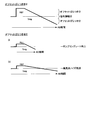
- FIG. 2 is an explanatory diagram showing an example in which the AD conversion time is compared between the case where there is offset variation and the case where there is no offset variation.
- the AD conversion method shown in FIG. 2 is a method in which the single-slope AD converter realizes AD conversion by comparing a reference signal that changes with time and an input analog signal (differential amplifier output), and has a signal amplitude range. In addition to this, it is necessary to secure a range for offset variation. As shown in FIG. 2, an increase in the AD conversion time means a decrease in the sampling rate. If there is no offset variation, high frequency noise can be reduced by lengthening the AD conversion time, but if there is offset variation, the AD conversion time should be further increased to reduce high frequency noise. It will be necessary.
- the Discloser has diligently studied the architecture of the potential measuring device to break the trade-off between low noise, high sampling rate, and high resolution. As a result, the Discloser has come up with an architecture of a potential measuring device that suppresses noise deterioration, sampling rate deterioration, and offset variation, as described below.
- the potential measuring device according to the embodiment of the present disclosure has a structure in which a second substrate on which the AD conversion circuit array is arranged is laminated on a substrate (first substrate) on which the electrode array is arranged.
- the potential measuring device according to the embodiment of the present disclosure is characterized in that an area for an AD conversion circuit is secured directly under the electrode.
- the potential measuring device can improve the sampling rate by reducing the wiring capacity, and further, an amplifier associated with substantially equalizing the wiring length that is different for each cell. It is also possible to improve the sampling rate by reducing the offset variation of the output.
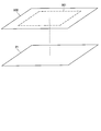
- FIG. 3 is an explanatory diagram showing a schematic configuration of the potential measuring device according to the embodiment of the present disclosure.
- the potential measuring device 1 shown in FIG. 3 has a structure in which the first substrate 100 and the second substrate 200 are laminated.
- the first substrate 100 includes a readout electrode array 900 in which electrodes 902 are arranged in an array.
- the second substrate 200 includes an AD conversion circuit array 22 so as to correspond to the readout electrode array 900 of the first substrate 100.
- AD conversion circuit array 22 AD conversion circuits 21 provided corresponding to each electrode of the first substrate 100 are arranged in an array.
- the readout electrode array 900 and the AD conversion circuit array 22 are connected with electrical continuity. For this connection with electrical continuity, for example, wafer level Cu-Cu bonding technology can be used.
- the wiring length between the electrode 902 and the AD conversion circuit corresponding to the electrode is substantially equal in all cells. can do.
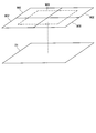
- FIG. 4 is an explanatory diagram showing a schematic configuration of a first substrate 100 of the potential measuring device 1 according to the embodiment of the present disclosure.
- the components of the readout electrode array 900 provided on the first substrate 100 are the electrodes 902 and the amplifier circuits 901 arranged in the same number as the electrodes 902 at the same pitch as the electrodes 902.
- a reference electrode 910 is arranged outside the read electrode array 900.
- the reference electrode 910 is an electrode intended to give a reference potential to the culture medium (medium) of the cells to be measured, which is immersed in the reading electrode array 900.
- the potential measuring device 1 according to the embodiment of the present disclosure measures the displacement from the reference potential supplied by the reference electrode 910 as the action potential of the cell to be measured.
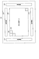
- FIG. 5 is an explanatory diagram showing a schematic configuration of a second substrate 200 of the potential measuring device 1 according to the embodiment of the present disclosure.
- the first substrate 100 is laminated on the second substrate 200.
- the AD conversion circuit array 22 is arranged on the second substrate 200 so as to correspond to the readout electrode array 900 of the first substrate 100.
- Various circuits necessary for operating the AD conversion circuit 21 are arranged outside the AD conversion circuit array 22.
- the AD conversion circuit array 22 is also provided with a time code transfer unit 23 that transfers the time code generated by the time code generation unit 26 to each AD conversion circuit 21.
- a pixel drive circuit 24 Around the AD conversion circuit array 22 on the second substrate 200, a pixel drive circuit 24, a DAC (D / A Converter) 25, a time code generator 26, a vertical drive circuit 27, an output unit 28, and a timing are used.
- the generation circuit 29 is formed.
- the AD conversion circuit 21 arranged in a two-dimensional array converts the analog signal from the electrode 902 into a digital signal SIG and outputs it.
- the pixel drive circuit 24 drives the AD conversion circuit 21.
- the DAC 25 generates a reference signal (reference voltage signal) REF, which is a slope signal whose level (voltage) monotonically decreases with the passage of time, and supplies the REF to each AD conversion circuit 21.
- the time code generation unit 26 generates a time code used when each AD conversion circuit 21 converts an analog signal into a digital signal (AD conversion), and supplies the time code to the corresponding time code transfer unit 23.
- a plurality of time code generation units 26 are provided for the AD conversion circuit array 22, and as many time code transfer units 23 as the number corresponding to the time code generation units 26 are provided in the AD conversion circuit array 22. ing. That is, the time code generation unit 26 and the time code transfer unit 23 that transfers the time code generated there have a one-to-one correspondence.
- the vertical drive circuit 27 controls the output unit 28 to output the digital signal SIG generated in the AD conversion circuit 21 to the output unit 28 in a predetermined order based on the timing signal supplied from the timing generation circuit 29.
- the digital signal SIG output from the AD conversion circuit 21 is output from the output unit 28 to the outside of the potential measuring device 1.
- the output unit 28 performs predetermined digital signal processing such as black level correction processing for correcting the black level and CDS (Correlated Double Sampling; correlation double sampling) processing as necessary, and then outputs the digital signal to the outside.
- the timing generation circuit 29 is configured by a timing generator or the like that generates various timing signals, and supplies the generated various timing signals to the pixel drive circuit 24, the DAC 25, the vertical drive circuit 27, and the like.
- FIG. 6 is an explanatory diagram showing a circuit block diagram from the electrode 902 to the AD conversion circuit 21 which is configured to straddle the first substrate 100 and the second substrate 200.
- FIG. 7 is an explanatory diagram showing an outline of a laminated structure of the electrode 902, the amplifier circuit 901, and the AD conversion circuit 21.
- the circuit model of the electrode 902 the simplest model in which the capacitance Cdl, which mainly represents the effect of the electric double layer capacitance, and the resistor Rct, which mainly represents the effect of the charge transfer resistance, are connected in parallel is adopted.
- An amplifier circuit 901 with an open loop gain of -A times is connected to the subsequent stage of the electrode 902.
- the input / output of the amplifier circuit 901 is connected to the amplifier circuit 901 via a feedback resistor Rfb.
- the feedback resistor Rfb for example, a non-doped polysilicon resistor or the like can be used. More preferably, the feedback resistor Rfb can be configured as a variable resistor.
- a reset switch transistor is connected to the input / output of the amplifier circuit 901 so that the input / output of the amplifier circuit 901 can be short-circuited at the time of reset, and the reset transistor is controlled to be turned on and off by the signal Amp_RST.
- the output wiring of the amplifier circuit 901 is passed to the second board 200.
- the analog signal from the amplifier circuit 901 is first sent to the comparison circuit 51 of the AD conversion circuit 21.
- the comparison circuit 51 compares the reference signal REF supplied from the DAC 25 with the analog signal sent from the amplifier circuit 901 of the first substrate 100, and outputs an output signal VCO as a comparison result signal representing the comparison result.
- the comparison circuit 51 inverts the output signal VCO when the reference signal REF and the analog signal are the same (voltage).
- the comparison circuit 51 is composed of a differential input circuit 61, a voltage conversion circuit 62, and a positive feedback circuit (PFB: positive fedback) 63.
- PFB positive fedback
- the output signal VCO is input from the comparison circuit 51 to the data storage unit 52, and the WORD signal that controls the read timing of the AD conversion circuit 21 during the signal read operation is supplied from the vertical drive circuit 27. Further, the time code generated by the time code generation unit 26 is also supplied via the time code transfer unit 23.
- the data storage unit 52 includes a latch control circuit 241 that controls the writing operation and the reading operation of the time code based on the WORD signal, and a latch storage unit 242 that stores the time code.
- the latch control circuit 241 is updated every unit time supplied from the time code transfer unit 23 while the Hi (High) output signal VCO is input from the comparison circuit 51.
- the time code is stored in the latch storage unit 242.
- the latch storage unit 242 holds the time code stored in the latch storage unit 242.
- the time code stored in the latch storage unit 242 represents the time when the analog signal and the reference signal REF become equal, and the data indicating that the analog signal was the reference voltage at that time, that is, digitized. Represents the light intensity value.
- the operation of the AD conversion circuit 21 changes from the write operation to the read operation. Be changed.
- the latch control circuit 241 stores the time stored in the latch storage unit 242 when the AD conversion circuit 21 reaches its own reading timing based on the WORD signal that controls the reading timing.
- the code (digital signal SIG) is output to the time code transfer unit 23.
- the time code transfer unit 23 sequentially transfers the supplied time code in the column direction (vertical direction) and supplies it to the output unit 28.
- the following is an inverted time code when the output signal VCO read from the latch storage unit 242 is inverted in the time code reading operation in order to distinguish it from the time code written in the latch storage unit 242 in the time code writing operation.
- the digitized data indicating that the analog signal was the reference voltage at that time is also referred to as AD conversion data.
- the bidirectional buffer circuit 37 is provided corresponding to the shift register included in the time code transfer unit 23.
- the bidirectional buffer circuit 371 is connected to one D flip-flop in the corresponding shift register.
- the bidirectional buffer circuit 371 is supplied with a write control signal WR that becomes Hi in the time code writing operation, and a read control signal RD that becomes Hi in the time code reading operation.
- the bidirectional buffer circuit 371 switches between a time code writing operation and a reading operation based on the write control signal WR and the read control signal RD.
- the analog signal from the amplifier circuit 901 is connected to the inverting input terminal of the differential input circuit 61 of the comparison circuit 51 of the first stage of the AD conversion circuit 21 via the DC cut capacitance Caz.
- the DC cut capacitance Caz is provided when the comparison circuit 51 is reset (also referred to as ode zero AZ). By performing this reset operation, it is possible to cancel the input offset caused by the manufacturing variation of the comparison circuit 51.
- the potential measuring device 1 may have a configuration in which one amplifier circuit 901 and an AD conversion circuit 21 correspond to a plurality of electrodes 902.
- FIG. 8 is an explanatory diagram showing a circuit block diagram from the electrode 902 to the AD conversion circuit 21 which is configured to straddle the first substrate 100 and the second substrate 200.
- FIG. 8 shows an example in which one amplifier circuit 901 and an AD conversion circuit 21 correspond to four electrodes 902.
- FIG. 9 is an explanatory diagram showing an outline of a laminated structure of four electrodes 902, one amplifier circuit 901, and one AD conversion circuit 21.
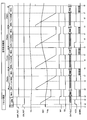
- FIG. 10 is an explanatory diagram showing the operation of the potential measuring device 1 according to the embodiment of the present disclosure in a timing chart.
- the potential measuring device 1 requires a reset period prior to the signal acquisition period.
- the reset period corresponds to times t1 to t5.
- the signal acquisition period corresponds to time t5 or later.
- the potential measuring device 1 continuously acquires signals of a plurality of frames (for example, several hundred frames) during the signal acquisition period.
- the potential measuring device 1 according to the embodiment of the present disclosure then inserts a reset period again as a refresh. Then, the potential measuring device 1 according to the embodiment of the present disclosure drives to start the signal acquisition period again.
- the potential measuring device 1 starts the reset operation of the amplifier circuit and the comparison circuit at time t1 during the reset period. At the following time t2, the potential measuring device 1 ends the reset of the comparison circuit and starts the AD conversion of the reset level. Therefore, the reference signal REF and the write enable signal WR to the latch storage unit of the time code DATA [n]. Launch. At time t3, the slope-changing REF and Vsig cross and the comparator output VCO is inverted. Along with this, the time code DATA [n] written in the latch storage unit 242 at that time is stored in the latch storage unit 242. This stored time code becomes the reset level AD conversion result.
- the reset level AD conversion period ends, the reset signals Amp_RST and WR of the amplifier circuit 901 are turned off, and instead, the AD conversion result stored in the latch storage unit 242 is enabled to be read out to the time code transfer unit 23.
- the signal RD is launched.
- the period from time t4 to t5 is a period in which the reset level AD conversion result is read out to the time code transfer unit 23 by the WORD signal and read out to the output unit 28 via the time code transfer unit 23.
- the reset period ends and the first frame of the signal acquisition period starts.
- the reset period except that the reset signal Amp_RST of the amplifier circuit 901 and the reset signal CM_RST of the comparison circuit 51 are not driven and the AD conversion time is long (due to the wider signal level range than the reset level). Is similar to.
- Times t5, t6 and t7 correspond to times t2, t3 and t4, respectively. After that, the operations at times t5 to t7 are repeated, so the description thereof will be omitted.
- a frame memory is arranged in the output unit 28, the AD conversion result of the reset level acquired during the reset period is held, and the signal acquired during the signal acquisition period.
- Correlated double sampling (CDS) can also be realized by taking the difference from the AD conversion result of the level.
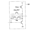
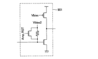
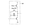
- 11 to 14 are explanatory views showing a circuit configuration example of the amplifier circuit 901.
- a feedback resistor Rfb and a reset transistor driven by an Amp_RST signal are connected to the source grounded amplifier circuit.
- the amplifier circuit 901 shown in FIG. 12 uses a bidirectional constantly OFF transistor as the feedback resistor Rfb.
- a bidirectional constantly OFF transistor as the feedback resistor Rfb, the feedback resistor Rfb of the amplifier circuit 901 can obtain a high resistance value in a small area.
- the amplifier circuit 901 shown in FIG. 13 has the same configuration as the example shown in FIG. 11 except for the circuit configuration of the amplifier.
- the input node of the amplifier is connected to the bias voltage Vbias2 via a resistor.
- the bias voltage Vbias2 is a bias voltage that can be arbitrarily set by the user. Therefore, the amplifier circuit 901 shown in FIG. 13 allows the user to arbitrarily adjust the operating point of the amplifier.
- the amplifier circuit 901 shown in FIG. 14 has the same configuration as the example shown in FIG. 11 except for the circuit configuration of the amplifier.
- the amplifier circuit 901 shown in FIG. 14 uses a source follower circuit instead of the grounded source amplifier circuit.
- the amplifier circuit 901 shown in FIG. 14 can be used in an expanded range by using a source follower circuit as an amplifier. Expanding the range of use is useful when measuring cells that emit large-amplitude signals compared to nerve cells, such as cardiomyocytes.
- FIG. 15 is an explanatory diagram showing a circuit configuration from the electrode 902 to the comparison circuit 51.
- FIG. 15 is a circuit diagram showing details of an electrode 902 and one amplifier circuit 901 added to the comparison circuit 51 shown in FIG.
- the differential input circuit 61 compares the signal SIG output from the amplifier circuit 901 with the reference signal REF output from the DAC 25, and outputs a predetermined signal (current) when the signal SIG is higher than the reference signal REF. To do.
- the differential input circuit 61 includes transistors 81 and 82 as differential pairs, transistors 83 and 84 constituting the current mirror, transistors 85 as a constant current source for supplying a current IB corresponding to the input bias current Vb, and a difference. It is composed of a transistor 86 that outputs an output signal HVO of the dynamic input circuit 61.
- Transistors 81, 82, and 85 are composed of NMOS (Negative Channel MOS) transistors, and transistors 83, 84, and 86 are composed of MOSFET (Positive Channel MOS) transistors.
- the reference signal REF output from the DAC 25 is input to the gate of the transistor 81, and the signal SIG output from the amplifier circuit 901 is input to the gate of the transistor 82.
- the source of the transistor 81 and the transistor 82 is connected to the drain of the transistor 85, and the source of the transistor 85 is connected to a predetermined voltage VSS (VSS ⁇ VDD2 ⁇ VDD1).
- the drain of the transistor 81 is connected to the gate of the transistors 83 and 84 and the drain of the transistor 83 constituting the current mirror circuit, and the drain of the transistor 82 is connected to the drain of the transistor 84 and the gate of the transistor 86.
- the sources of transistors 83, 84, and 86 are connected to a first supply voltage VDD1.
- the voltage conversion circuit 62 is composed of, for example, an NMOS type transistor 91.
- the drain of the transistor 91 is connected to the drain of the transistor 86 of the differential input circuit 61, the source of the transistor 91 is connected to a predetermined connection point in the positive feedback circuit 63, and the gate of the transistor 86 is connected to the bias voltage VBIAS. It is connected.
- the transistors 81 to 86 constituting the differential input circuit 61 are circuits that operate at a high voltage up to the first power supply voltage VDD1, and the positive feedback circuit 63 has a second power supply voltage VDD2 that is lower than the first power supply voltage VDD1. It is a working circuit.
- the voltage conversion circuit 62 converts the output signal HVO input from the differential input circuit 61 into a low voltage signal (conversion signal) LVI in which the positive feedback circuit 63 can operate, and supplies the output signal HVO to the positive feedback circuit 63.
- the bias voltage VBIAS may be any voltage that converts the transistors 101 to 105 of the positive feedback circuit 63 that operates at a constant voltage into a voltage that does not destroy them.
- the positive feedback circuit 63 inverts when the signal SIG is higher than the reference signal REF based on the conversion signal LVI in which the output signal HVO from the differential input circuit 61 is converted into a signal corresponding to the second power supply voltage VDD2. Output the comparison result signal. Further, the positive feedback circuit 63 speeds up the transition speed when the output signal VCO output as the comparison result signal is inverted.
- the positive feedback circuit 63 is composed of five transistors 101 to 105.
- the transistors 101, 102, and 104 are composed of MOSFET transistors, and the transistors 103 and 105 are composed of NMOS transistors.
- the source of the transistor 91 which is the output end of the voltage conversion circuit 62, is connected to the drain of the transistors 102 and 103 and the gate of the transistors 104 and 105.
- the source of the transistors 101 and 104 is connected to the second power supply voltage VDD2
- the drain of the transistor 101 is connected to the source of the transistor 102
- the gate of the transistor 102 is the output end of the positive feedback circuit 63. It is connected to the drain of.
- the sources of transistors 103 and 105 are connected to a predetermined voltage VSS.
- the initialization signal INI is supplied to the gates of the transistors 101 and 103.
- the transistors 104 and 105 form an inverter circuit, and the connection point between the drains thereof is an output end at which the comparison circuit 51 outputs an output signal VCO.
- FIG. 16 is an explanatory diagram showing a circuit configuration from the data storage unit 52 to the time code transfer unit 23.
- the time code transfer unit 23 is composed of N shift registers 341-1 to 341-N corresponding to the N-bit time codes DATA [1] to DATA [N] and a clock supply circuit 342.
- Each of the N shift registers 341-1 to 341-N is composed of a plurality of DF / F (D-flip-flops) 351.
- the clock supply circuit 342 supplies the clock signal CLK to the clock input of each DF / F351 of the shift register 341.
- the data storage unit 52 is composed of a latch control circuit 241 and N bit storage units 242-1 to 242-N. Further, N bidirectional buffer circuits 371-1 to 371-N are provided between the time code transfer unit 23 and the data storage unit 52.
- the N bidirectional buffer circuits 371-1 to 371-N are provided in the N shift registers 341-1 to 341-N of the time code transfer unit 23 in a one-to-one correspondence.
- the bidirectional buffer circuit 371 is connected to one DF / F351 in the corresponding shift register 341.
- a write control signal WR that becomes Hi in the time code writing operation is supplied to the buffer circuit 381 of the bidirectional buffer circuit 371-n, and a read control signal RD that becomes Hi in the time code reading operation is supplied to the inverter circuit 382. Is supplied.
- the bidirectional buffer circuit 371-n switches between a time code writing operation and a reading operation for the bit storage unit 242-n based on the write control signal WR and the read control signal RD.
- One latch control circuit 241 supplies output signals VCO and WORD signals to N bit storage units 242-1 to 242-N.
- Each of the bit storage units 242-1 to 242-N is composed of a transfer gate 261 and a latch storage unit 262.
- the latch control circuit 241 is composed of two inverters 281 and 282 connected in series, and a NOR circuit 283 and an inverter 284 connected in series.
- the transfer gate 261 of the bit storage unit 242-n is composed of two transistors 291 and 292, which are an NMOS transistor and a MOSFET transistor.
- the latch storage unit 262 of the bit storage unit 242-n is composed of a static type latch circuit composed of transistors 301 to 306.
- Transistors 301, 302, and 305 are composed of MOSFET transistors, and transistors 303, 304, and 306 are composed of NMOS transistors.
- the output signal VCO which is the output from the comparison circuit 51, is input to the inverter 281 and the NOR circuit 283, and the WORD signal is supplied to the other input of the NOR circuit 283.
- the output of the inverter 281 is supplied to the gate of the inverter 282 and the transistor 303 of the latch storage unit 262, and the output of the inverter 282 is supplied to the gate of the transistor 302 of the latch storage unit 262.
- the output of the NOR circuit 283 is supplied to the gate of the inverter 284 and the transistor 292 of the transfer gate 261, and the output of the inverter 284 is supplied to the gate of the transistor 291 of the transfer gate 261.
- the N shift registers 341 of the time code transfer unit 23 clock the time code supplied from the time code generation unit 26 and the unit time of the time code. Transfer with the shift clock.
- the Hi write control signal WR and the Lo read control signal RD are supplied to the bidirectional buffer circuit 371, and the bidirectional buffer circuit 371 is set to the predetermined D- of the shift register 341.
- the time code supplied from the F / F 351 is supplied to the bit storage unit 242 via the transfer gate 261.
- the bit storage unit 242 stores the supplied time code.
- the time code stored in the bit storage unit 242 is supplied to a predetermined DF / F351 of the shift register 341 of the time code transfer unit 23 via the bidirectional buffer circuit 371. Will be done.
- the shift register 341 sequentially transfers the time data supplied to the DF / F351 of each stage to the output unit 28 and outputs the time data.
- the clock signal CLK supplied to the clock input is described as a high impedance state (hereinafter referred to as HiZ state) in either Hi or Lo. .) Is adopted.
- HiZ state a high impedance state
- the DF / F351 is in the HiZ state when the clock signal CLK is Lo.
- the Hi read control signal RD is supplied to the bidirectional buffer circuit 371, the WORD signal becomes Hi, and the bit storage unit 242.
- the time code stored in is supplied to a predetermined DF / F351 of the shift register 341 of the time code transfer unit 23 via the bidirectional buffer circuit 371.
- FIG. 17 is an explanatory diagram showing a circuit configuration of flip flip of the shift register used in the time code transfer unit 23.
- characters such as on and off marked in parentheses () near each transistor and signal line indicate the potential state of each transistor and signal line when the Lo clock signal CLK is input to the clock input. It shows.
- FIG. 18 is an explanatory diagram showing the circuit configuration of the front stage portion of the comparison circuit 51 of the first stage of the electrode 902, the amplifier circuit 901, and the AD conversion circuit 21 by extracting it.
- the relationship between Vin and Vsig is shown as follows.
- the frequency characteristic with respect to the gain shows the high-pass filter (HPF) characteristic as shown in FIG.
- HPF high-pass filter
- the signal band is said to be several hundred Hz to several kHz, and it is desirable that the gain outside the signal band is reduced from the viewpoint of noise characteristics. It is considered that the above HPF characteristics can suppress low frequency noise on the medium.
- the noise on the high frequency side can be suppressed by the low-pass filter (LPF) characteristics of AD conversion.
- the gain in the signal band is obtained by dividing the open loop gain A of the amplifier circuit 901 by the inverse ratio of the DC cut capacitance Caz and the Vsig node parasitic capacitance Cin.
- the DC cut capacitance Caz can be reduced by increasing the open loop gain A of the amplifier circuit 901 with respect to the gain finally desired. Since the capacitance generally takes a large area, it is a great merit for the present embodiment in which the AD conversion circuit 21 must be mounted within the size of the electrode 902, which is about 10 ⁇ m square.
- the potential measuring device 1 has a structure in which a second substrate 200 on which an AD conversion circuit array is arranged is laminated on a first substrate 100 on which an electrode array is arranged. Has.
- the potential measuring device 1 according to the embodiment of the present disclosure minimizes the wiring length from the amplification circuit output to the AD conversion circuit, and makes each wiring substantially equal in length. be able to. Therefore, the potential measuring device 1 according to the embodiment of the present disclosure can improve the sampling rate by reducing the wiring capacity, and further, the wiring lengths that are different for each cell are substantially equalized. It is also possible to improve the sampling rate by reducing the offset variation of the amplifier output.
- an amplifier circuit is provided in a signal path from the read electrode to the AD conversion circuit.
- the potential measuring device is a source follower circuit including an amplifier transistor whose drain terminal is AC grounded and a load.
- the amplifier circuit is a source grounded amplifier circuit including an amplifier transistor and a load whose source terminals are AC grounded.
- the potential measuring device is a source grounded amplifier circuit including an amplifier transistor and a load whose source terminals are AC grounded.
- the potential measuring device according to (6) above, wherein the resistance value of the feedback resistor is variable.
- the potential measuring device according to (4) or (5) above, wherein a bias voltage is applied to the input of the amplifier circuit via a resistor.
- the AD conversion circuit includes a comparison circuit.
- an input signal is applied to one input via a DC cut capacitance, and a time-varying reference signal is applied to the other input.
- the potential measuring device described in. (10) A data storage unit that stores data according to the output of the comparison circuit, A data transfer circuit that writes data to the data storage unit and reads data from the data storage unit using the same circuit.
- the potential measuring device according to (9) above. (11) The potential measuring device according to any one of (1) to (10), wherein the AD conversion circuit is associated with a plurality of the readout electrodes.
Landscapes
- Engineering & Computer Science (AREA)
- Power Engineering (AREA)
- General Physics & Mathematics (AREA)
- Life Sciences & Earth Sciences (AREA)
- Physics & Mathematics (AREA)
- Chemical & Material Sciences (AREA)
- Organic Chemistry (AREA)
- Health & Medical Sciences (AREA)
- Bioinformatics & Cheminformatics (AREA)
- Zoology (AREA)
- Wood Science & Technology (AREA)
- Sustainable Development (AREA)
- Genetics & Genomics (AREA)
- Biotechnology (AREA)
- Biomedical Technology (AREA)
- Biochemistry (AREA)
- General Engineering & Computer Science (AREA)
- General Health & Medical Sciences (AREA)
- Microbiology (AREA)
- Analytical Chemistry (AREA)
- Cell Biology (AREA)
- Theoretical Computer Science (AREA)
- Analogue/Digital Conversion (AREA)
- Measurement Of Current Or Voltage (AREA)
- Apparatus Associated With Microorganisms And Enzymes (AREA)
- Measuring Leads Or Probes (AREA)
Abstract
読出し電極が2次元アレイ状に配置された第1の基板と、前記第1の基板が積層された第2の基板と、を備え、前記読出し電極のそれぞれは、独立に対応付けられた少なくとも1つのAD変換回路を備え、前記AD変換回路の少なくとも一部は前記第2の基板において2次元アレイ状に配置される、電位測定装置が提供される。
Description
本開示は、電位測定装置に関する。
微小電極をアレイ状に並べ、その微小電極上の溶液の電位を計測するデバイスがある。そのようなデバイスの中に、微小電極上を培養液で満たして生体細胞を乗せ、生体細胞が発生する活動電位を測定するデバイスがある(例えば特許文献1等参照)。特に近年では、CMOS(Complementary MOS)集積回路技術を用いて、電極と、増幅器やAD変換器などとを一つのチップにまとめ、多点で同時に電位を測定するデバイスが注目されている(例えば非特許文献1等参照)。
神経細胞の活動電位波形の取得を考えると、10kHz程度以上のサンプリングレートを確保した上で数μVクラスの低ノイズ計測が必要と考えられる。さらに、神経細胞ネットワーク内の信号伝搬を詳細かつ広範囲に取得するためには、電極サイズを10μm角程度として密に敷き詰め、高解像度化する必要がある。低ノイズ化、高サンプリングレート化、高解像度化はそれぞれトレードオフの関係にあり、これらのトレードオフを打破するため回路アーキテクチャにおいて様々な提案が行われている(例えば非特許文献1等参照)。
低ノイズかつ高解像度化を実現するための有望な手法のひとつとして、電極毎に差動増幅回路を持ちながらも、差動増幅回路を構成する片側の増幅回路領域(参照回路領域)を、電極で受けた信号を読み出すもう一方の増幅回路領域(読出し回路領域)から分離する構成が提案されている(例えば非特許文献2等参照)。
M.Obien,et al., "Revealing neuronalfunction through microelectrode array recordings" ,Frontiers in Neuro ScienceVol.8 (2015) Article 423
J.Park,et al.," A High-Density CMOS Multi-Modality JointSensor/Stimulator Array with 1024 Pixels for Holistic Real-Time CellularCharacterization", Symposium on VLSI Circuits Digest of Technical Papers(2016)
しかし、この手法ではアンプ回路の読出し回路/参照回路、負荷PMOS、電流源NMOSと、A/D変換回路がそれぞれ物理的に離れて配置されるため、高解像度化に伴いアンプ回路の各ノード配線は長距離配線にならざるを得ない。長距離配線により、配線抵抗増大に起因するノイズ悪化や、配線容量増大に起因するサンプリングレートの悪化を招く。また、セル毎にアンプ回路の配線長が異なることに起因してオフセットばらつきが発生する。このオフセットばらつきのためAD期間が増大することもサンプリングレート悪化の一因となる。
そこで、本開示では、ノイズ悪化やサンプリングレート悪化、オフセットばらつきを抑えて、データ処理の容易性や解析精度を向上させることが可能な、新規かつ改良された電位測定装置を提案する。
本開示によれば、読出し電極が2次元アレイ状に配置された第1の基板と、前記第1の基板が積層された第2の基板と、を備え、前記読出し電極のそれぞれは、独立に対応付けられた少なくとも1つのAD変換回路を備え、前記AD変換回路の少なくとも一部は前記第2の基板において2次元アレイ状に配置される、電位測定装置が提供される。
以下に添付図面を参照しながら、本開示の好適な実施の形態について詳細に説明する。なお、本明細書及び図面において、実質的に同一の機能構成を有する構成要素については、同一の符号を付することにより重複説明を省略する。
なお、説明は以下の順序で行うものとする。
1.本開示の実施の形態
1.1.経緯
1.2.構成例及び動作例
2.まとめ
1.本開示の実施の形態
1.1.経緯
1.2.構成例及び動作例
2.まとめ
<1.本開示の実施の形態>
[1.1.経緯]
本開示の実施の形態について詳細に説明する前に、本開示者が本開示の実施の形態に至った経緯について説明する。
[1.1.経緯]
本開示の実施の形態について詳細に説明する前に、本開示者が本開示の実施の形態に至った経緯について説明する。
上述したように、CMOS集積回路技術を用いて、電極と、増幅器やAD変換器などとを一つのチップにまとめ、多点で同時に電位を測定するデバイスが近年注目されている。低ノイズ化、高サンプリングレート化、高解像度化はそれぞれトレードオフの関係にあるが、これらのトレードオフを打破するため回路アーキテクチャに関する様々な提案がなされている。
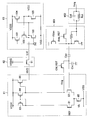
図1は、既存の電位測定装置の回路構成例を示す説明図である。図1に示した電位測定装置1020は多点で同時に電位を検出することが可能なデバイスであり、読出し回路領域と参照回路領域とを分離した構成を有する。図1に示した電位測定装置1020は、A/D変換回路1021と、垂直選択回路1023と、読み出しセル領域1101及び参照セル領域1102とからなる半導体デバイスと、を有する。また図1には、カレントミラーを構成するMOSFET Tr1a、1bと、電流源1140と、が示されている。
A/D変換回路1021は、半導体デバイスによって測定されたアナログのデータをデジタルのデータに変換する回路である。垂直選択回路1023は、半導体デバイスに対して電位の測定に使用される読み出しセルや参照セルの選択を行うための信号を出力する回路である。
このような構成を有する電位測定装置において、初段の差動増幅回路である程度の増幅ゲインを得ることで、入力換算ノイズを低減できる。しかし、初段の差動増幅回路である程度の増幅ゲインを得ると、初段の増幅器としてソースフォロア回路を用いた場合と比較して出力抵抗が高くなる。さらに、サンプリングレートを高く維持したまま高解像度化をするためには、AD変換回路の並列数を上げる必要があり、高出力抵抗である差動増幅回路の出力を電極アレイ外に配置されるAD変換回路まで長距離配線(すなわち高寄生容量)で接続する必要がある。
このように、読出し回路領域と参照回路領域とを分離した構成の場合、参照回路領域における差動増幅回路の出力と、AD変換回路との距離が長距離となる。したがって、差動増幅回路出力のセトリング時間が悪化し、サンプリングレートの向上に対しては相性が良くない。
また、AD変換回路の並列数を上げたことで電極アレイの幅とAD変換回路の領域の幅の整合がとれない場合、電極により配線長が大きく異なるため、配線抵抗起因の差動増幅器出力のオフセットばらつきが発生する。ここで、小面積で構成可能なシングルスロープ型のAD変換器を前提として考えると、差動増幅器出力のオフセットばらつきの増加はAD変換時間の増加に直結することになる。
図2は、AD変換時間を、オフセットばらつきがある場合と、無い場合とを比較した例を示す説明図である。図2に示したAD変換方式は、シングルスロープAD変換器が時間的に変化する参照信号と入力アナログ信号(差動増幅器出力)を比較することでAD変換を実現する方式であり、信号振幅レンジに加えてオフセットばらつき分のレンジを確保する必要があるためである。図2に示したように、AD変換時間の増加は、すなわちサンプリングレートの低下を意味する。またオフセットばらつきが無い場合は、AD変換時間を長時間化することで高周波ノイズの低減も可能となるが、オフセットばらつきがある場合は、高周波ノイズの低減のためにはさらなるAD変換時間の増加を要することになる。
そこで本件開示者は、上述した点に鑑み、低ノイズ化、高サンプリングレート化、高解像度化のトレードオフを打破するための電位測定装置のアーキテクチャについて鋭意検討を行った。その結果、本件開示者は、以下で説明するように、ノイズ悪化やサンプリングレート悪化、オフセットばらつきを抑えた電位測定装置のアーキテクチャを考案するに至った。
[1.2.構成例及び動作例]
次に、本開示の実施の形態に係る電位測定装置の構成例について説明する。本開示の実施の形態に係る電位測定装置は、電極アレイが配置される基板(第1の基板)に対し、AD変換回路アレイが配置される第2の基板を積層した構造を有する。本開示の実施の形態に係る電位測定装置は、電極の直下にAD変換回路用の面積を確保したことを特徴とする。本開示の実施の形態に係る電位測定装置は、このような構成を有することで、増幅回路出力からAD変換回路までの配線長を最小限にし、かつ、それぞれの配線を略等長化することができる。従って、本開示の実施の形態に係る電位測定装置は、配線容量を削減することによるサンプリングレートの向上が可能となり、さらに、セル毎に異なっていた配線長を略等長化することに伴う増幅器出力のオフセットばらつきの低減によるサンプリングレートの向上も可能となる。
次に、本開示の実施の形態に係る電位測定装置の構成例について説明する。本開示の実施の形態に係る電位測定装置は、電極アレイが配置される基板(第1の基板)に対し、AD変換回路アレイが配置される第2の基板を積層した構造を有する。本開示の実施の形態に係る電位測定装置は、電極の直下にAD変換回路用の面積を確保したことを特徴とする。本開示の実施の形態に係る電位測定装置は、このような構成を有することで、増幅回路出力からAD変換回路までの配線長を最小限にし、かつ、それぞれの配線を略等長化することができる。従って、本開示の実施の形態に係る電位測定装置は、配線容量を削減することによるサンプリングレートの向上が可能となり、さらに、セル毎に異なっていた配線長を略等長化することに伴う増幅器出力のオフセットばらつきの低減によるサンプリングレートの向上も可能となる。
図3は、本開示の実施の形態に係る電位測定装置の概略構成を示す説明図である。図3に示した電位測定装置1は、上述したように、第1の基板100と、第2の基板200とが積層された構造を有する。第1の基板100は、電極902がアレイ状に配置された読出し電極アレイ900を備える。また第2の基板200は、第1の基板100の読出し電極アレイ900に対応するようにAD変換回路アレイ22を備える。AD変換回路アレイ22は、第1の基板100の各電極に対応して設けられるAD変換回路21がアレイ状に配置されている。読出し電極アレイ900と、AD変換回路アレイ22とは、が電気的導通をもって接続される。この電気的導通をもった接続には、例えばウェハレベルCu-Cuボンディング技術を用いることができる。そして第1の基板100と、第2の基板200とが積層された構造を有することで、電極902と、その電極に対応するAD変換回路との間の配線長は、全てのセルにおいて略等しくすることができる。
図4は、本開示の実施の形態に係る電位測定装置1の第1の基板100の概略構成を示す説明図である。第1の基板100に設けられる読出し電極アレイ900の構成要素は、電極902、及び、電極902と同じピッチで電極902と同数配置される増幅回路901である。また、読出し電極アレイ900の外側には基準電極910が配置される。基準電極910は、読出し電極アレイ900に浸される、測定対象の細胞の培養液(培地)に対して、基準となる電位を与えることを目的とした電極である。本開示の実施の形態に係る電位測定装置1は、基準電極910が供給する基準電位からの変位を、測定対象の細胞の活動電位として測定するものである。
図5は、本開示の実施の形態に係る電位測定装置1の第2の基板200の概略構成を示す説明図である。第2の基板200は、上述したように第1の基板100が積層される。第2の基板200には、第1の基板100の読出し電極アレイ900に対応するようにAD変換回路アレイ22が配置される。AD変換回路アレイ22の外側にはAD変換回路21を動作させるために必要な各種回路が配置される。
AD変換回路アレイ22には、時刻コード発生部26で生成された時刻コードを各AD変換回路21に転送する時刻コード転送部23も設けられている。そして、第2の基板200上のAD変換回路アレイ22の周辺には、画素駆動回路24、DAC(D/A Converter)25、時刻コード発生部26、垂直駆動回路27、出力部28、及びタイミング生成回路29が形成されている。
2次元アレイ状に配列されたAD変換回路21は、電極902からのアナログ信号をデジタル信号SIGに変換して出力する。
画素駆動回路24は、AD変換回路21を駆動する。DAC25は、時間経過に応じてレベル(電圧)が単調減少するスロープ信号である参照信号(基準電圧信号)REFを生成し、各AD変換回路21に供給する。時刻コード発生部26は、各AD変換回路21が、アナログ信号をデジタルの信号に変換(AD変換)する際に使用される時刻コードを生成し、対応する時刻コード転送部23に供給する。時刻コード発生部26は、AD変換回路アレイ22に対して複数個設けられており、AD変換回路アレイ22内には、時刻コード発生部26に対応する数だけ、時刻コード転送部23が設けられている。即ち、時刻コード発生部26と、そこで生成された時刻コードを転送する時刻コード転送部23は、1対1に対応する。
垂直駆動回路27は、AD変換回路21内で生成されたデジタル信号SIGを、タイミング生成回路29から供給されるタイミング信号に基づいて、所定の順番で出力部28に出力させる制御を行う。AD変換回路21から出力されたデジタル信号SIGは、出力部28から電位測定装置1の外部へ出力される。出力部28は、黒レベルを補正する黒レベル補正処理やCDS(Correlated Double Sampling;相関2重サンプリング)処理など、所定のデジタル信号処理を必要に応じて行い、その後、外部へ出力する。
タイミング生成回路29は、各種のタイミング信号を生成するタイミングジェネレータなどによって構成され、生成した各種のタイミング信号を、画素駆動回路24、DAC25、垂直駆動回路27等に供給する。
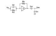
図6は、第1の基板100と第2の基板200とを跨いで構成される、電極902からAD変換回路21までの回路ブロック図を示す説明図である。また図7は、電極902及び増幅回路901と、AD変換回路21との積層構造の概要を示す説明図である。電極902の回路モデルとしては、主に電気二重層容量の効果を表す容量Cdlと、主に電荷移動抵抗の効果を表す抵抗Rctとを並列接続した、最も単純なモデルを採用している。
電極902の後段には、オープンループゲインが-A倍の増幅回路901が接続される。増幅回路901には、フィードバック抵抗Rfbを介してその入出力が接続されている。フィードバック抵抗Rfbには、例えばノンドープのポリシリコン抵抗等を用いることができる。さらに望ましくは、フィードバック抵抗Rfbは可変抵抗として構成されうる。また増幅回路901の入出力には、リセット時に増幅回路901の入出力を短絡できるようにリセット用のスイッチトランジスタが接続され、このリセットトランジスタは信号Amp_RSTでオン、オフが制御される。
増幅回路901の出力配線は、第2の基板200へと渡される。増幅回路901からのアナログ信号は、まずAD変換回路21の比較回路51に送られる。比較回路51は、DAC25から供給される参照信号REFと、第1の基板100の増幅回路901から送られるアナログ信号とを比較し、比較結果を表す比較結果信号として、出力信号VCOを出力する。比較回路51は、参照信号REFとアナログ信号が同一(の電圧)になったとき、出力信号VCOを反転させる。
比較回路51は、差動入力回路61、電圧変換回路62、及び正帰還回路(PFB:positive feedback)63により構成される。
データ記憶部52には、比較回路51から出力信号VCOが入力される他、垂直駆動回路27から、信号の読み出し動作中におけるAD変換回路21の読み出しタイミングを制御するWORD信号が供給される。また、時刻コード転送部23を介して、時刻コード発生部26で生成された時刻コードも供給される。
データ記憶部52は、WORD信号に基づいて、時刻コードの書き込み動作と読み出し動作を制御するラッチ制御回路241と、時刻コードを記憶するラッチ記憶部242で構成される。
ラッチ制御回路241は、時刻コードの書き込み動作においては、比較回路51からHi(High)の出力信号VCOが入力されている間、時刻コード転送部23から供給される、単位時間ごとに更新される時刻コードをラッチ記憶部242に記憶させる。そして、参照信号REFと信号SIGが同一(の電圧)になり、比較回路51から供給される出力信号VCOがLo(Low)に反転されたとき、供給される時刻コードの書き込み(更新)を中止し、最後にラッチ記憶部242に記憶された時刻コードをラッチ記憶部242に保持させる。ラッチ記憶部242に記憶された時刻コードは、アナログ信号と参照信号REFが等しくなった時刻を表しており、アナログ信号がその時刻の基準電圧であったことを示すデータ、即ち、デジタル化された光量値を表す。
参照信号REFの掃引が終了し、AD変換回路アレイ22内の全てのAD変換回路21のラッチ記憶部242に時刻コードが記憶された後、AD変換回路21の動作が、書き込み動作から読み出し動作に変更される。
ラッチ制御回路241は、時刻コードの読み出し動作においては、読み出しタイミングを制御するWORD信号に基づいて、AD変換回路21が自分の読み出しタイミングとなったときに、ラッチ記憶部242に記憶されている時刻コード(デジタル信号SIG)を、時刻コード転送部23に出力する。時刻コード転送部23は、供給された時刻コードを、列方向(垂直方向)に順次転送し、出力部28に供給する。
以下では、時刻コードの書き込み動作においてラッチ記憶部242に書き込まれる時刻コードと区別するため、時刻コードの読み出し動作においてラッチ記憶部242から読み出される出力信号VCOが反転したときの反転時刻コードである、アナログ信号がその時刻の基準電圧であったことを示すデジタル化されたデータを、AD変換データとも称する。
双方向バッファ回路37は、時刻コード転送部23に含まれるシフトレジスタに対応して設けられている。双方向バッファ回路371は、対応するシフトレジスタ内の1つのDフリップフロップと接続されている。
双方向バッファ回路371には、時刻コードの書き込み動作においてHiとなる書き込み制御信号WRが供給され、時刻コードの読み出し動作においてHiとなる読み出し制御信号RDが供給される。双方向バッファ回路371は、書き込み制御信号WRと読み出し制御信号RDに基づいて時刻コードの書き込み動作と読み出し動作を切り替える。
増幅回路901からのアナログ信号は、DCカット容量Cazを介してAD変換回路21の初段の比較回路51の差動入力回路61の反転入力端子へと接続される。DCカット容量Cazは、比較回路51のリセット動作(オードゼロAZとも呼ばれる)を行う場合は設けられる。このリセット動作を行うことで、比較回路51の製造ばらつきに起因する入力オフセットをキャンセルすることができる。
なお、ここまでは1つの電極902に1つの増幅回路901及び1つのAD変換回路21が対応している例を示したが、本開示は係る例に限定されるものではない。電位測定装置1は、複数の電極902に1つの増幅回路901及びAD変換回路21が対応するような構成を有していても良い。
図8は、第1の基板100と第2の基板200とを跨いで構成される、電極902からAD変換回路21までの回路ブロック図を示す説明図である。図8に示したのは、4つの電極902に1つの増幅回路901及びAD変換回路21が対応する例である。図9は、4つの電極902及び1つの増幅回路901と、1つのAD変換回路21との積層構造の概要を示す説明図である。
続いて、本開示の実施の形態に係る電位測定装置1の動作例を説明する。図10は、本開示の実施の形態に係る電位測定装置1の動作をタイミングチャートで示す説明図である。
本開示の実施の形態に係る電位測定装置1は、信号取得期間に先立ってリセット期間が必要となる。リセット期間は時刻t1~t5に相当する。信号取得期間は時刻t5以降に相当する。
本開示の実施の形態に係る電位測定装置1は、信号取得期間において、複数フレーム(例えば数百フレーム)の信号を連続して取得する。本開示の実施の形態に係る電位測定装置1は、その後、リフレッシュとして再度リセット期間を挿入する。そして本開示の実施の形態に係る電位測定装置1は、再び信号取得期間を開始するという駆動を行う。
本開示の実施の形態に係る電位測定装置1は、リセット期間では、時刻t1において増幅回路と比較回路のリセット動作を開始する。電位測定装置1は、続く時刻t2で、比較回路のリセットを終了し、リセットレベルのAD変換を開始するため、リファレンス信号REFと、時刻コードDATA[n]のラッチ記憶部への書き込みイネーブル信号WRを立ち上げる。時刻t3において、スロープ状に変化するREFとVsigがクロスし比較器出力VCOが反転する。それに伴い、その時点でラッチ記憶部242に書き込まれていた時刻コードDATA[n]がラッチ記憶部242に記憶されることになる。この記憶された時刻コードがリセットレベルのAD変換結果となる。
時刻t4において、リセットレベルのAD変換期間が終了し、増幅回路901のリセット信号Amp_RSTとWRが立ち下げられ、代わりにラッチ記憶部242に記憶されたAD変換結果を時刻コード転送部23へ読み出すイネーブル信号RDが立ち上げられる。時刻t4からt5の期間は、WORD信号によりリセットレベルのAD変換結果を時刻コード転送部23へ読出し、時刻コード転送部23を経由して出力部28へと読み出す期間である。
時刻t5において、リセット期間が終了し、信号取得期間の1フレーム目が開始される。増幅回路901のリセット信号Amp_RSTと比較回路51のリセット信号CM_RSTの駆動が無いことと、(リセットレベルより信号レベルのレンジが広いことに起因して)AD変換の時間が長いこと以外は、リセット期間と同様である。
時刻t5,t6,t7が、それぞれ、時刻t2,t3,t4に対応する。以降は時刻t5~t7の動作が繰り返しになるため説明は省略する。
なお、本開示の実施の形態に係る電位測定装置1は、出力部28にフレームメモリを配置し、リセット期間に取得したリセットレベルのAD変換結果を保持しておき、信号取得期間に取得する信号レベルのAD変換結果との差分を取ることで、相関二重サンプリング(CDS)を実現することも可能である。
図11~図14は、増幅回路901の回路構成例を示す説明図である。
図11に示した増幅回路901は、ソース接地増幅回路にフィードバック抵抗RfbとAmp_RST信号で駆動されるリセットトランジスタが接続されている。
図12に示した増幅回路901は、フィードバック抵抗Rfbとして双方向の常時OFFトランジスタを用いている。フィードバック抵抗Rfbとして双方向の常時OFFトランジスタを用いることで、増幅回路901のフィードバック抵抗Rfbは小面積で高い抵抗値を得ることができる。
図13に示した増幅回路901は、増幅器の回路構成以外は図11に示した例と同様の構成である。図13に示した増幅回路901は、フィードバック抵抗Rfbの代わりに、増幅器の入力ノードが抵抗を介してバイアス電圧Vbias2に接続されている。バイアス電圧Vbias2は、ユーザが任意に設定できるバイアス電圧である。従って、図13に示した増幅回路901は、増幅器の動作点をユーザが任意に調整することが可能になる。
図14に示した増幅回路901は、増幅器の回路構成以外は図11に示した例と同様の構成である。図14に示した増幅回路901は、ソース接地増幅回路の代わりにソースフォロア回路を用いている。図14に示した増幅回路901は、増幅器としてソースフォロア回路を用いることで使用レンジを拡大することができる。使用レンジの拡大は、心筋細胞のように、神経細胞と比較し大振幅の信号を発する細胞を測定する際に有用である。
図15は、電極902から比較回路51までの回路構成を示す説明図である。
図15は、図6に示した比較回路51に、電極902及び1つの増幅回路901の詳細を追加して示した回路図である。
差動入力回路61は、増幅回路901から出力された信号SIGと、DAC25から出力された参照信号REFとを比較し、信号SIGが参照信号REFよりも高いときに所定の信号(電流)を出力する。
差動入力回路61は、差動対となるトランジスタ81及び82、カレントミラーを構成するトランジスタ83及び84、入力バイアス電流Vbに応じた電流IBを供給する定電流源としてのトランジスタ85、並びに、差動入力回路61の出力信号HVOを出力するトランジスタ86により構成されている。
トランジスタ81、82、及び85は、NMOS(Negative Channel MOS)トランジスタで構成され、トランジスタ83、84、及び86は、PMOS(Positive Channel MOS)トランジスタで構成される。
差動対となるトランジスタ81、82のうち、トランジスタ81のゲートには、DAC25から出力された参照信号REFが入力され、トランジスタ82のゲートには、増幅回路901から出力された信号SIGが入力される。トランジスタ81とトランジスタ82のソースは、トランジスタ85のドレインと接続され、トランジスタ85のソースは、所定の電圧VSS(VSS<VDD2<VDD1)に接続されている。
トランジスタ81のドレインは、カレントミラー回路を構成するトランジスタ83、84のゲート及びトランジスタ83のドレインと接続され、トランジスタ82のドレインは、トランジスタ84のドレイン及びトランジスタ86のゲートと接続されている。トランジスタ83、84、及び86のソースは、第1電源電圧VDD1に接続されている。
電圧変換回路62は、例えば、NMOS型のトランジスタ91で構成される。トランジスタ91のドレインは、差動入力回路61のトランジスタ86のドレインと接続され、トランジスタ91のソースは、正帰還回路63内の所定の接続点に接続され、トランジスタ86のゲートは、バイアス電圧VBIASに接続されている。
差動入力回路61を構成するトランジスタ81~86は、第1電源電圧VDD1までの高電圧で動作する回路であり、正帰還回路63は、第1電源電圧VDD1よりも低い第2電源電圧VDD2で動作する回路である。電圧変換回路62は、差動入力回路61から入力される出力信号HVOを、正帰還回路63が動作可能な低電圧の信号(変換信号)LVIに変換して、正帰還回路63に供給する。
バイアス電圧VBIASは、定電圧で動作する正帰還回路63の各トランジスタ101~105を破壊しない電圧に変換する電圧であれば良い。例えば、バイアス電圧VBIASは、正帰還回路63の第2電源電圧VDD2と同じ電圧(VBIAS=VDD2)とすることができる。
正帰還回路63は、差動入力回路61からの出力信号HVOが第2電源電圧VDD2に対応する信号に変換された変換信号LVIに基づいて、信号SIGが参照信号REFよりも高いときに反転する比較結果信号を出力する。また、正帰還回路63は、比較結果信号として出力する出力信号VCOが反転するときの遷移速度を高速化する。
正帰還回路63は、5つのトランジスタ101~105で構成される。ここで、トランジスタ101、102、及び104は、PMOSトランジスタで構成され、トランジスタ103及び105は、NMOSトランジスタで構成される。
電圧変換回路62の出力端であるトランジスタ91のソースは、トランジスタ102及び103のドレインと、トランジスタ104及び105のゲートに接続されている。トランジスタ101及び104のソースは、第2電源電圧VDD2に接続され、トランジスタ101のドレインは、トランジスタ102のソースと接続され、トランジスタ102のゲートは、正帰還回路63の出力端でもあるトランジスタ104及び105のドレインと接続されている。トランジスタ103及び105のソースは、所定の電圧VSSに接続されている。トランジスタ101と103のゲートには、初期化信号INIが供給される。
トランジスタ104と105はインバータ回路を構成し、それらのドレイン同士の接続点は、比較回路51が出力信号VCOを出力する出力端となっている。
図16は、データ記憶部52から時刻コード転送部23の回路構成を示す説明図である。
時刻コード転送部23が、Nビットの時刻コードDATA[1]~DATA[N]に対応するN個のシフトレジスタ341-1~341-Nと、クロック供給回路342とで構成されている。N個のシフトレジスタ341-1~341-Nそれぞれは、複数のD-F/F(D-フリップフロップ)351からなる。クロック供給回路342は、シフトレジスタ341の各D-F/F351のクロック入力に、クロック信号CLKを供給する。
データ記憶部52は、ラッチ制御回路241と、N個のビット記憶部242-1~242-Nと、で構成されている。さらに時刻コード転送部23とデータ記憶部52との間に、N個の双方向バッファ回路371-1~371-Nが設けられている。
N個の双方向バッファ回路371-1~371-Nは、時刻コード転送部23のN個のシフトレジスタ341-1~341-Nに1対1に対応して設けられている。双方向バッファ回路371は、対応するシフトレジスタ341内の1つのD-F/F351と接続されている。
双方向バッファ回路371-nのバッファ回路381には、時刻コードの書き込み動作においてHiとなる書き込み制御信号WRが供給され、インバータ回路382には、時刻コードの読み出し動作においてHiとなる読み出し制御信号RDが供給される。双方向バッファ回路371-nは、書き込み制御信号WRと読み出し制御信号RDに基づいて、ビット記憶部242-nに対する時刻コードの書き込み動作と読み出し動作を切り替える。
1個のラッチ制御回路241が、N個のビット記憶部242-1~242-Nに、出力信号VCOとWORD信号を供給する。ビット記憶部242-1~242-Nそれぞれは、トランスファゲート261とラッチ記憶部262で構成される。
ラッチ制御回路241は、直列接続された2個のインバータ281及び282と、直列接続されたNOR回路283及びインバータ284で構成されている。
ビット記憶部242-nのトランスファゲート261は、NMOSトランジスタとPMOSトランジスタの2個のトランジスタ291及び292で構成されている。
ビット記憶部242-nのラッチ記憶部262は、トランジスタ301乃至306からなるスタティック型のラッチ回路で構成されている。トランジスタ301、302、及び305は、PMOSトランジスタで構成され、トランジスタ303、304、及び306は、NMOSトランジスタで構成されている。
比較回路51からの出力である出力信号VCOは、インバータ281とNOR回路283に入力され、NOR回路283のもう一方の入力には、WORD信号が供給される。インバータ281の出力は、インバータ282とラッチ記憶部262のトランジスタ303のゲートに供給され、インバータ282の出力は、ラッチ記憶部262のトランジスタ302のゲートに供給される。また、NOR回路283の出力は、インバータ284とトランスファゲート261のトランジスタ292のゲートに供給され、インバータ284の出力は、トランスファゲート261のトランジスタ291のゲートに供給される。
参照信号REFの掃引が行われるAD変換期間中には、時刻コード転送部23のN個のシフトレジスタ341は、時刻コード発生部26から供給された時刻コードを、時刻コードの単位時間をクロック周期とするシフトクロックで転送する。
時刻コードの書き込み動作においては、Hiの書き込み制御信号WRと、Loの読み出し制御信号RDが、双方向バッファ回路371に供給されており、双方向バッファ回路371は、シフトレジスタ341の所定のD-F/F351から供給された時刻コードを、トランスファゲート261を介してビット記憶部242に供給する。ビット記憶部242は、供給された時刻コードを記憶する。
次の時刻コードの読み出し動作においては、ビット記憶部242に記憶されている時刻コードが、双方向バッファ回路371を介して時刻コード転送部23のシフトレジスタ341の所定のD-F/F351に供給される。シフトレジスタ341は、各段のD-F/F351に供給された時刻データを順送りに出力部28まで転送し、出力する。
より具体的には、シフトレジスタ341の各D-F/F351には、クロック入力に供給されるクロック信号CLKがHiまたはLoのいずれか一方でハイインピーダンス状態(以下、Hi-Z状態と記述する。)にできる構成が採用される。例えば、図17で後述するD-F/F351の構成では、D-F/F351は、クロック信号CLKがLoであるとき、Hi-Z状態となる。
シフトレジスタ341の各D-F/F351がHi-Z状態とされている期間に、双方向バッファ回路371にHiの読み出し制御信号RDが供給されるとともに、WORD信号がHiとなり、ビット記憶部242に記憶されている時刻コードが、双方向バッファ回路371を介して時刻コード転送部23のシフトレジスタ341の所定のD-F/F351に供給される。
読み出し制御信号RDがLoに戻された後、シフトレジスタ341の各D-F/F351にシフトクロックが供給され、シフトレジスタ341は、各段のD-F/F351に供給された時刻データを出力部28まで順次転送し、出力する。
図17は、時刻コード転送部23で用いられるシフトレジスタのフリップフリップの回路構成を示す説明図である。
図17において、各トランジスタや信号線の近傍に括弧()付で記したon、off等の文字は、Loのクロック信号CLKがクロック入力に入力されたときの各トランジスタや信号線の電位状態を示している。
図17に示されるように、Loのクロック信号CLKがD-F/F351に入力された場合には、D-F/F351がHi-Z状態となる。
続いて、電極902の微小電位変動VinがAD変換回路21の初段の比較回路51の入力ノードVsigに至るまでの伝達関数について検討する。図18は、電極902、増幅回路901、AD変換回路21の初段の比較回路51の前段部分の回路構成を抜き出して示す説明図である。VinとVsigとの関係は、以下のように示される。

信号周波数が1/2πRctCdlより極めて小さい低周波領域では、

である。さらに、A>>1、A>>Rfb/Rctである場合は、

である。一方、信号周波数が(Rfb+Rct(1+A))/2πRfbRctCdlより極めて大きい高周波領域では、

となる。これらから、ゲインに対する周波数特性は図19に示すようなハイパスフィルタ(HPF)特性を示す。神経細胞の活動電位を取得する場合、その信号帯域は数百Hz~数kHzと言われており、ノイズ特性観点では信号帯域外のゲインは落ちていることが望ましい。上記のHPF特性により、培地に乗っている低周波ノイズを抑制できると考えられる。なお、高周波側のノイズはAD変換のローパスフィルタ(LPF)特性により抑制可能である。
また、上記の式から、信号帯域におけるゲインは増幅回路901のオープンループゲインAをDCカット容量CazとVsigノード寄生容量Cinの逆比で分圧した形になることが分かる。言い換えると、最終的に得たいゲインに対して、増幅回路901のオープンループゲインAを大きく取ることで、DCカット容量Cazを小さくすることができる。一般に容量は大きな面積を取ることから、10μm角程度である電極902のサイズ内にAD変換回路21を搭載しなければいけない本実施形態にとって大きなメリットである。
<2.まとめ>
以上説明したように本開示の実施の形態によれば、ノイズ悪化やサンプリングレート悪化、オフセットばらつきを抑えた電位測定装置1を提供することが出来る。具体的には、本開示の実施の形態に係る電位測定装置1は、電極アレイが配置される第1の基板100に対し、AD変換回路アレイが配置される第2の基板200を積層した構造を有する。
以上説明したように本開示の実施の形態によれば、ノイズ悪化やサンプリングレート悪化、オフセットばらつきを抑えた電位測定装置1を提供することが出来る。具体的には、本開示の実施の形態に係る電位測定装置1は、電極アレイが配置される第1の基板100に対し、AD変換回路アレイが配置される第2の基板200を積層した構造を有する。
本開示の実施の形態に係る電位測定装置1は、このような構成を有することで、増幅回路出力からAD変換回路までの配線長を最小限にし、かつ、それぞれの配線を略等長化することができる。従って、本開示の実施の形態に係る電位測定装置1は、配線容量を削減することによるサンプリングレートの向上が可能となり、さらに、セル毎に異なっていた配線長を略等長化することに伴う増幅器出力のオフセットばらつきの低減によるサンプリングレートの向上も可能となる。
以上、添付図面を参照しながら本開示の好適な実施形態について詳細に説明したが、本開示の技術的範囲はかかる例に限定されない。本開示の技術分野における通常の知識を有する者であれば、請求の範囲に記載された技術的思想の範疇内において、各種の変更例または修正例に想到し得ることは明らかであり、これらについても、当然に本開示の技術的範囲に属するものと了解される。
また、本明細書に記載された効果は、あくまで説明的または例示的なものであって限定的ではない。つまり、本開示に係る技術は、上記の効果とともに、または上記の効果に代えて、本明細書の記載から当業者には明らかな他の効果を奏しうる。
なお、以下のような構成も本開示の技術的範囲に属する。
(1)
読出し電極が2次元アレイ状に配置された第1の基板と、
前記第1の基板が積層された第2の基板と、
を備え、
前記読出し電極のそれぞれは、独立に対応付けられた少なくとも1つのAD変換回路を備え、前記AD変換回路の少なくとも一部は前記第2の基板において2次元アレイ状に配置される、電位測定装置。
(2)
前記読出し電極から前記AD変換回路までの信号経路の配線長がほぼ同一となるよう配線される、前記(1)に記載の電位測定装置。
(3)
前記読出し電極から前記AD変換回路までの信号経路に増幅回路を備える、前記(2)に記載の電位測定装置。
(4)
前記増幅回路は、ドレイン端子が交流的に接地されたアンプトランジスタと、負荷と、で構成されるソースフォロア回路である、前記(3)に記載の電位測定装置。
(5)
前記増幅回路は、ソース端子が交流的に接地されたアンプトランジスタ、負荷と、で構成されるソース接地増幅回路である、前記(3)に記載の電位測定装置。
(6)
前記増幅回路の入出力がフィードバック抵抗により接続されている、前記(4)または(5)に記載の電位測定装置。
(7)
前記フィードバック抵抗の抵抗値は可変である、前記(6)に記載の電位測定装置。
(8)
前記増幅回路の入力に、抵抗を介してバイアス電圧が印加される、前記(4)または(5)に記載の電位測定装置。
(9)
前記AD変換回路は、比較回路を含み、
前記比較回路は、一方の入力にはDCカット容量を介して入力信号が印加され、もう一方の入力には時間的に変化する参照信号が印加される、前記(1)~(8)のいずれかに記載の電位測定装置。
(10)
前記比較回路の出力に応じデータ記憶を行うデータ記憶部と、
前記データ記憶部へのデータ書き込み及び前記データ記憶部からのデータ読出しを同一の回路で行うデータ転送回路と、
をさらに備える、前記(9)に記載の電位測定装置。
(11)
前記AD変換回路は、複数の前記読出し電極に対応付けられる、前記(1)~(10)のいずれかに記載の電位測定装置。
(1)
読出し電極が2次元アレイ状に配置された第1の基板と、
前記第1の基板が積層された第2の基板と、
を備え、
前記読出し電極のそれぞれは、独立に対応付けられた少なくとも1つのAD変換回路を備え、前記AD変換回路の少なくとも一部は前記第2の基板において2次元アレイ状に配置される、電位測定装置。
(2)
前記読出し電極から前記AD変換回路までの信号経路の配線長がほぼ同一となるよう配線される、前記(1)に記載の電位測定装置。
(3)
前記読出し電極から前記AD変換回路までの信号経路に増幅回路を備える、前記(2)に記載の電位測定装置。
(4)
前記増幅回路は、ドレイン端子が交流的に接地されたアンプトランジスタと、負荷と、で構成されるソースフォロア回路である、前記(3)に記載の電位測定装置。
(5)
前記増幅回路は、ソース端子が交流的に接地されたアンプトランジスタ、負荷と、で構成されるソース接地増幅回路である、前記(3)に記載の電位測定装置。
(6)
前記増幅回路の入出力がフィードバック抵抗により接続されている、前記(4)または(5)に記載の電位測定装置。
(7)
前記フィードバック抵抗の抵抗値は可変である、前記(6)に記載の電位測定装置。
(8)
前記増幅回路の入力に、抵抗を介してバイアス電圧が印加される、前記(4)または(5)に記載の電位測定装置。
(9)
前記AD変換回路は、比較回路を含み、
前記比較回路は、一方の入力にはDCカット容量を介して入力信号が印加され、もう一方の入力には時間的に変化する参照信号が印加される、前記(1)~(8)のいずれかに記載の電位測定装置。
(10)
前記比較回路の出力に応じデータ記憶を行うデータ記憶部と、
前記データ記憶部へのデータ書き込み及び前記データ記憶部からのデータ読出しを同一の回路で行うデータ転送回路と、
をさらに備える、前記(9)に記載の電位測定装置。
(11)
前記AD変換回路は、複数の前記読出し電極に対応付けられる、前記(1)~(10)のいずれかに記載の電位測定装置。
1 :電位測定装置
21 :AD変換回路
22 :AD変換回路アレイ
23 :時刻コード転送部
24 :画素駆動回路
26 :時刻コード発生部
27 :垂直駆動回路
28 :出力部
29 :タイミング生成回路
37 :双方向バッファ回路
51 :比較回路
52 :データ記憶部
61 :差動入力回路
62 :電圧変換回路
63 :正帰還回路
900 :読出し電極アレイ
901 :増幅回路
902 :電極
910 :基準電極
21 :AD変換回路
22 :AD変換回路アレイ
23 :時刻コード転送部
24 :画素駆動回路
26 :時刻コード発生部
27 :垂直駆動回路
28 :出力部
29 :タイミング生成回路
37 :双方向バッファ回路
51 :比較回路
52 :データ記憶部
61 :差動入力回路
62 :電圧変換回路
63 :正帰還回路
900 :読出し電極アレイ
901 :増幅回路
902 :電極
910 :基準電極
Claims (11)
- 読出し電極が2次元アレイ状に配置された第1の基板と、
前記第1の基板が積層された第2の基板と、
を備え、
前記読出し電極のそれぞれは、独立に対応付けられた少なくとも1つのAD変換回路を備え、前記AD変換回路の少なくとも一部は前記第2の基板において2次元アレイ状に配置される、電位測定装置。 - 前記読出し電極から前記AD変換回路までの信号経路の配線長がほぼ同一となるよう配線される、請求項1に記載の電位測定装置。
- 前記読出し電極から前記AD変換回路までの信号経路に増幅回路を備える、請求項2に記載の電位測定装置。
- 前記増幅回路は、ドレイン端子が交流的に接地されたアンプトランジスタと、負荷と、で構成されるソースフォロア回路である、請求項3に記載の電位測定装置。
- 前記増幅回路は、ソース端子が交流的に接地されたアンプトランジスタ、負荷と、で構成されるソース接地増幅回路である、請求項3に記載の電位測定装置。
- 前記増幅回路の入出力がフィードバック抵抗により接続されている、請求項4に記載の電位測定装置。
- 前記フィードバック抵抗の抵抗値は可変である、請求項6に記載の電位測定装置。
- 前記増幅回路の入力に、抵抗を介してバイアス電圧が印加される、請求項4に記載の電位測定装置。
- 前記AD変換回路は、比較回路を含み、
前記比較回路は、一方の入力にはDCカット容量を介して入力信号が印加され、もう一方の入力には時間的に変化する参照信号が印加される、請求項1に記載の電位測定装置。 - 前記比較回路の出力に応じデータ記憶を行うデータ記憶部と、
前記データ記憶部へのデータ書き込み及び前記データ記憶部からのデータ読出しを同一の回路で行うデータ転送回路と、
をさらに備える、請求項9に記載の電位測定装置。 - 前記AD変換回路は、複数の前記読出し電極に対応付けられる、請求項1に記載の電位測定装置。
Priority Applications (1)
| Application Number | Priority Date | Filing Date | Title |
|---|---|---|---|
| US17/435,315 US12007420B2 (en) | 2019-03-19 | 2020-02-28 | Potential measurement device |
Applications Claiming Priority (2)
| Application Number | Priority Date | Filing Date | Title |
|---|---|---|---|
| JP2019-051653 | 2019-03-19 | ||
| JP2019051653A JP2020153778A (ja) | 2019-03-19 | 2019-03-19 | 電位測定装置 |
Publications (1)
| Publication Number | Publication Date |
|---|---|
| WO2020189222A1 true WO2020189222A1 (ja) | 2020-09-24 |
Family
ID=72520772
Family Applications (1)
| Application Number | Title | Priority Date | Filing Date |
|---|---|---|---|
| PCT/JP2020/008226 Ceased WO2020189222A1 (ja) | 2019-03-19 | 2020-02-28 | 電位測定装置 |
Country Status (3)
| Country | Link |
|---|---|
| US (1) | US12007420B2 (ja) |
| JP (1) | JP2020153778A (ja) |
| WO (1) | WO2020189222A1 (ja) |
Cited By (2)
| Publication number | Priority date | Publication date | Assignee | Title |
|---|---|---|---|---|
| CN115078812A (zh) * | 2022-05-10 | 2022-09-20 | 浙江诺尔康神经电子科技股份有限公司 | 一种mri兼容电极电压测试电路 |
| WO2026078999A1 (ja) * | 2024-10-08 | 2026-04-16 | ソニーセミコンダクタソリューションズ株式会社 | 電極アレイセンサおよび電極アレイセンサシステム |
Citations (10)
| Publication number | Priority date | Publication date | Assignee | Title |
|---|---|---|---|---|
| JPS59126306A (ja) * | 1983-01-10 | 1984-07-20 | Nippon Telegr & Teleph Corp <Ntt> | 広帯域電界効果トランジスタ増幅器 |
| JPH09246880A (ja) * | 1996-03-05 | 1997-09-19 | Nippon Telegr & Teleph Corp <Ntt> | 増幅回路 |
| JP2002055144A (ja) * | 2000-05-23 | 2002-02-20 | Tektronix Inc | 信号検出装置及び方法 |
| JP2014049983A (ja) * | 2012-08-31 | 2014-03-17 | Canon Inc | 放射線撮像装置、その制御方法及びプログラム |
| JP2014195112A (ja) * | 2005-06-02 | 2014-10-09 | Sony Corp | 半導体イメージセンサ・モジュール及びその製造方法 |
| US20150138153A1 (en) * | 2010-02-05 | 2015-05-21 | Broadcom Corporation | Systems and methods for providing enhanced touch sensing |
| JP2016019235A (ja) * | 2014-07-10 | 2016-02-01 | 株式会社半導体理工学研究センター | 増幅回路、cmosインバータ増幅回路、比較回路、δςアナログデジタル変換器、及び半導体装置 |
| JP2016171455A (ja) * | 2015-03-12 | 2016-09-23 | 株式会社東芝 | 固体撮像装置 |
| WO2016152267A1 (ja) * | 2015-03-24 | 2016-09-29 | ソニー株式会社 | 増幅器および電子回路 |
| JP2017507653A (ja) * | 2014-03-25 | 2017-03-23 | ジェニア・テクノロジーズ・インコーポレイテッド | 積層型ウェハ技術を用いたナノポアベースのシーケンシングチップ |
Family Cites Families (6)
| Publication number | Priority date | Publication date | Assignee | Title |
|---|---|---|---|---|
| JP3909738B2 (ja) | 2000-07-13 | 2007-04-25 | 松下電器産業株式会社 | 細胞外記録用一体化複合電極 |
| US8049293B2 (en) | 2005-03-07 | 2011-11-01 | Sony Corporation | Solid-state image pickup device, electronic apparatus using such solid-state image pickup device and method of manufacturing solid-state image pickup device |
| JP4802520B2 (ja) | 2005-03-07 | 2011-10-26 | ソニー株式会社 | 固体撮像装置及びその製造方法 |
| JP2016028408A (ja) * | 2014-03-24 | 2016-02-25 | パナソニックIpマネジメント株式会社 | 蓄電素子及び蓄電素子の製造方法 |
| US9785821B2 (en) * | 2015-08-28 | 2017-10-10 | Synaptics Incorporated | Capacitive sensor architecture for biometric sensing |
| JP2019056581A (ja) * | 2017-09-20 | 2019-04-11 | ソニーセミコンダクタソリューションズ株式会社 | 電荷検出センサおよび電位計測システム |
-
2019
- 2019-03-19 JP JP2019051653A patent/JP2020153778A/ja active Pending
-
2020
- 2020-02-28 WO PCT/JP2020/008226 patent/WO2020189222A1/ja not_active Ceased
- 2020-02-28 US US17/435,315 patent/US12007420B2/en active Active
Patent Citations (10)
| Publication number | Priority date | Publication date | Assignee | Title |
|---|---|---|---|---|
| JPS59126306A (ja) * | 1983-01-10 | 1984-07-20 | Nippon Telegr & Teleph Corp <Ntt> | 広帯域電界効果トランジスタ増幅器 |
| JPH09246880A (ja) * | 1996-03-05 | 1997-09-19 | Nippon Telegr & Teleph Corp <Ntt> | 増幅回路 |
| JP2002055144A (ja) * | 2000-05-23 | 2002-02-20 | Tektronix Inc | 信号検出装置及び方法 |
| JP2014195112A (ja) * | 2005-06-02 | 2014-10-09 | Sony Corp | 半導体イメージセンサ・モジュール及びその製造方法 |
| US20150138153A1 (en) * | 2010-02-05 | 2015-05-21 | Broadcom Corporation | Systems and methods for providing enhanced touch sensing |
| JP2014049983A (ja) * | 2012-08-31 | 2014-03-17 | Canon Inc | 放射線撮像装置、その制御方法及びプログラム |
| JP2017507653A (ja) * | 2014-03-25 | 2017-03-23 | ジェニア・テクノロジーズ・インコーポレイテッド | 積層型ウェハ技術を用いたナノポアベースのシーケンシングチップ |
| JP2016019235A (ja) * | 2014-07-10 | 2016-02-01 | 株式会社半導体理工学研究センター | 増幅回路、cmosインバータ増幅回路、比較回路、δςアナログデジタル変換器、及び半導体装置 |
| JP2016171455A (ja) * | 2015-03-12 | 2016-09-23 | 株式会社東芝 | 固体撮像装置 |
| WO2016152267A1 (ja) * | 2015-03-24 | 2016-09-29 | ソニー株式会社 | 増幅器および電子回路 |
Cited By (2)
| Publication number | Priority date | Publication date | Assignee | Title |
|---|---|---|---|---|
| CN115078812A (zh) * | 2022-05-10 | 2022-09-20 | 浙江诺尔康神经电子科技股份有限公司 | 一种mri兼容电极电压测试电路 |
| WO2026078999A1 (ja) * | 2024-10-08 | 2026-04-16 | ソニーセミコンダクタソリューションズ株式会社 | 電極アレイセンサおよび電極アレイセンサシステム |
Also Published As
| Publication number | Publication date |
|---|---|
| US20220137106A1 (en) | 2022-05-05 |
| US12007420B2 (en) | 2024-06-11 |
| JP2020153778A (ja) | 2020-09-24 |
Similar Documents
| Publication | Publication Date | Title |
|---|---|---|
| JP3507800B2 (ja) | アナログ−デジタル変換器及びこれを用いたイメージセンサ | |
| JP2013540259A (ja) | アレイ列積分器 | |
| WO2020189222A1 (ja) | 電位測定装置 | |
| US7696911B2 (en) | Amplifier circuit, digital-to-analog conversion circuit, and display device | |
| US20190080660A1 (en) | Half-Power Buffer and/or Amplifier | |
| JP6919651B2 (ja) | 半導体装置および細胞電位測定装置 | |
| JPH02282788A (ja) | 表示駆動回路 | |
| CN100525112C (zh) | 具有晶片上参考电压产生器的半导体装置 | |
| JP4785848B2 (ja) | オートズーム式傾斜型ad変換器 | |
| CN102111125A (zh) | 具有电流输出型放大单元的信号发生器 | |
| CN109361883B (zh) | 像素读出电路及图像传感器 | |
| CN101527549B (zh) | 具电压内插功能的放大器电路 | |
| JP2011205393A (ja) | 固体撮像装置および固体撮像装置の駆動方法 | |
| TWI227965B (en) | True/complement-phase logic signal pair generation device | |
| US6044036A (en) | Buffer circuit, memory device, and integrated circuit for receiving digital signals | |
| Ashoori et al. | Multichannel Potentiostat with Shared Reference Electrode for Simultaneous Multitechnique Measurements in Microfluidic Sensor Arrays | |
| JP3176860B2 (ja) | 信号伝達回路、信号伝達方法、a/d変換器および固体撮像素子 | |
| CN111654253B (zh) | 一种信号采集与放大电路阵列 | |
| CN108011636A (zh) | 一种用于时间交织adc的直流耦合通道校准电路 | |
| CN117118407B (zh) | 一种带二维地址调制tot脉冲功能的时间测量电路 | |
| TWI259433B (en) | Source driver and liquid crystal display | |
| TWI384752B (zh) | Buffer amplifiers and flat panel display devices | |
| JP2001027919A (ja) | レシーバ回路 | |
| Lay et al. | Pre-amplifier arrays for intra-oral ultrasound probe receiving electronics | |
| JP3909570B2 (ja) | Ad変換器の入力回路 |
Legal Events
| Date | Code | Title | Description |
|---|---|---|---|
| 121 | Ep: the epo has been informed by wipo that ep was designated in this application |
Ref document number: 20773785 Country of ref document: EP Kind code of ref document: A1 |
|
| NENP | Non-entry into the national phase |
Ref country code: DE |
|
| 122 | Ep: pct application non-entry in european phase |
Ref document number: 20773785 Country of ref document: EP Kind code of ref document: A1 |