WO2020144746A1 - 積層セラミックコンデンサ用ニッケルペースト - Google Patents
積層セラミックコンデンサ用ニッケルペースト Download PDFInfo
- Publication number
- WO2020144746A1 WO2020144746A1 PCT/JP2019/000252 JP2019000252W WO2020144746A1 WO 2020144746 A1 WO2020144746 A1 WO 2020144746A1 JP 2019000252 W JP2019000252 W JP 2019000252W WO 2020144746 A1 WO2020144746 A1 WO 2020144746A1
- Authority
- WO
- WIPO (PCT)
- Prior art keywords
- nickel
- paste
- nickel paste
- internal electrode
- ceramic capacitor
- Prior art date
- Legal status (The legal status is an assumption and is not a legal conclusion. Google has not performed a legal analysis and makes no representation as to the accuracy of the status listed.)
- Ceased
Links
Classifications
-
- H—ELECTRICITY
- H01—ELECTRIC ELEMENTS
- H01B—CABLES; CONDUCTORS; INSULATORS; SELECTION OF MATERIALS FOR THEIR CONDUCTIVE, INSULATING OR DIELECTRIC PROPERTIES
- H01B1/00—Conductors or conductive bodies characterised by the conductive materials; Selection of materials as conductors
- H01B1/20—Conductive material dispersed in non-conductive organic material
- H01B1/22—Conductive material dispersed in non-conductive organic material the conductive material comprising metals or alloys
-
- H—ELECTRICITY
- H01—ELECTRIC ELEMENTS
- H01G—CAPACITORS; CAPACITORS, RECTIFIERS, DETECTORS, SWITCHING DEVICES, LIGHT-SENSITIVE OR TEMPERATURE-SENSITIVE DEVICES OF THE ELECTROLYTIC TYPE
- H01G4/00—Fixed capacitors; Processes of their manufacture
- H01G4/002—Details
- H01G4/018—Dielectrics
- H01G4/06—Solid dielectrics
- H01G4/08—Inorganic dielectrics
- H01G4/12—Ceramic dielectrics
-
- H—ELECTRICITY
- H01—ELECTRIC ELEMENTS
- H01G—CAPACITORS; CAPACITORS, RECTIFIERS, DETECTORS, SWITCHING DEVICES, LIGHT-SENSITIVE OR TEMPERATURE-SENSITIVE DEVICES OF THE ELECTROLYTIC TYPE
- H01G4/00—Fixed capacitors; Processes of their manufacture
- H01G4/30—Stacked capacitors
Definitions
- the present invention relates to a conductive paste, and more particularly, to a nickel paste used to form an internal electrode of a multi-layer ceramic capacitor (MLCC: Multi-Layer Ceramic Capacitor).
- MLCC Multi-Layer Ceramic Capacitor
- the monolithic ceramic capacitor has a structure in which ceramic dielectric layers and internal electrode layers are alternately laminated and sintered to be integrated.
- noble metals such as palladium have been conventionally used as the internal electrode material of the monolithic ceramic capacitor, but nowadays nickel is mainly used for cost reduction.
- the most effective means for achieving miniaturization, high capacity, and high performance is to make the nickel internal electrode layer and the ceramic dielectric layer thin to achieve a multilayer structure.
- a laminated ceramic capacitor is manufactured, for example, by the following manufacturing process.
- a nickel paste in which nickel powder as an internal electrode material is dispersed in a vehicle containing an organic resin binder and a solvent is prepared.
- a ceramic green sheet is prepared by dispersing a dielectric powder such as barium titanate (BaTiO 3 ) as a main component in an organic resin binder and then drying it. After printing the nickel paste on this green sheet, it is dried to remove the solvent and form a dry film to be an internal electrode.
- the green sheets on which the dried films are formed in this manner are stacked in multiple layers, and are thermocompression bonded to be integrated.
- the integrated dielectric block is cut into a predetermined chip size, and then, in order to remove the organic resin binder, heat treatment is performed at a temperature of 500° C. or less in an oxidizing atmosphere or an inert atmosphere to remove the binder, and then the binder is removed.
- the nickel internal electrode layer and the ceramic dielectric layer are integrally sintered by heating to a temperature of about 1300° C. in a reducing atmosphere so as to prevent the internal electrode from being oxidized and firing.
- a conductive paste for external electrodes is applied to both end faces of the sintered chip and baked at about 800°C. Then, the surface of the external electrode is plated to obtain a monolithic ceramic capacitor.
- the temperature at which the ceramic dielectric layer sinters and starts shrinking is about 1200° C., which is higher than the temperature at which the conductive powder such as nickel sinters and starts shrinking. Due to the large difference in shrinkage behavior between the body layer and the nickel internal electrode layer, structural defects such as delamination and cracks may occur. In particular, as the number of stacked layers increases or the thickness of the ceramic dielectric layer becomes thinner, the occurrence of structural defects becomes more prominent as the size and the capacity are increased.
- Patent Document 1 discloses that an electrode paste contains a ceramic powder as a co-material to control the interaction between the co-material and the dielectric layer during sintering.
- Patent Document 2 by using a nickel powder in which sulfur is contained even in the nickelaceous portion of the fine nickel powder, the heat shrinkage start temperature is raised and the temperature between the dielectric layer and the internal electrode layer is increased.
- a technique is disclosed that reduces the generated stress and does not cause a break in the formed internal electrode film.
- Patent Document 3 by using nickel fine particles in which fine particles containing a precious metal element as a main component are scattered on the surface of the fine particles containing a nickel element as a main component, the sintering resistance of the nickel fine particles is improved, A technique for suppressing the contraction of the electrode layer and the breakage of the internal electrode film is disclosed.
- JP 2006-269320 A Japanese Patent Laid-Open No. 2014-091862 JP-A-2005-049973
- Patent Document 1 controls the firing shrinkage behavior by the interaction of the sintering of the co-material and the dielectric layer, and the co-material existing at the interface reacts with the dielectric layer and sticks to the internal electrode layer It is thought that the contraction of the is suppressed.
- shrinkage may be suppressed by this effect, but when the internal electrode layer becomes thin, it may cause cracks in the internal electrode layer near the fixed co-material, which is not preferable. ..
- Patent Document 2 raises the sintering start temperature of the internal electrode layers by adding sulfur to the nickel powder.
- the formed monolithic ceramic capacitors are good, but the various electronic components that are mounted at the same time are also becoming smaller and finer, and if the sulfur contained in the nickel powder is generated as outgas, This is not preferable because it may corrode high-definition parts.
- Patent Document 3 uses conductive particles in which fine particles containing a precious metal element as a main component are scattered on the surface of fine particles containing a nickel element as a main component. Amid the further miniaturization, it is not preferable to evenly disperse expensive precious metal fine particles so that the nickel powders are not sintered together, because the cost is technically and materially high.
- the present invention has been made in view of the above-mentioned conventional circumstances, does not utilize the interaction with the dielectric layer, and does not contain sulfur, which is not preferable for semiconductor parts, and does not contain expensive precious metals.
- the configuration by raising the sintering start temperature of the conductive paste to approach the sintering start temperature of the ceramic green sheet, it is possible to prevent structural defects such as delamination, cracks, and breakage of the internal electrode film in the firing process of the multilayer ceramic capacitor.
- An object of the present invention is to provide a nickel paste for a laminated ceramic capacitor, which can prevent generation at low cost and is suitable for forming a nickel internal electrode.
- a nickel paste for a multilayer ceramic capacitor according to the present invention is a nickel paste used for forming an internal electrode of a multilayer ceramic capacitor containing nickel powder, a dispersant, and an organic vehicle as a main component.
- the agent is characterized by containing a phosphate polyester.
- the content of the phosphoric acid polyester is preferably 0.3 part by mass or more and 3 parts by mass or less with respect to 100 parts by mass of the nickel powder.
- the sintering start temperature of the conductive paste is increased.
- the ceramic green sheet it is possible to inexpensively prevent the occurrence of structural defects such as delamination and cracks in the firing process of manufacturing the monolithic ceramic capacitor, and breaks in the internal electrode film. Therefore, it is possible to obtain a nickel paste for a laminated ceramic capacitor which can easily manufacture a laminated ceramic capacitor having no structural defect without controlling the shape and particle size of the nickel powder and regardless of the binder and the solvent used.
- the nickel paste for a multilayer ceramic capacitor of the present invention will be described in detail.
- the present inventor diligently studied the effect of various additive materials contained in the nickel paste on the shrinkage behavior of the nickel internal electrode layer, and found that the nickel paste contains a polyester phosphate. , Has an effect of increasing the sintering start temperature of the nickel paste, and has an effect of reducing the stress generated between the dielectric layer and the internal electrode layer as compared with the conventional nickel paste which does not contain polyester phosphate. Found.
- the phosphoric acid polyester when the phosphoric acid polyester is contained in the nickel paste, the phosphoric acid group is strongly adsorbed on the surface of the nickel powder in the nickel paste, and the long chain structure of the polyester connected to the phosphoric acid group prevents the agglomeration of the nickel powders. It is considered that the nickel powder can be uniformly dispersed in the nickel paste by suppressing the agglomeration of the nickel powders in the nickel paste. Further, since the phosphoric acid polyester has heat resistance and can maintain the state in which the agglomeration of the nickel powders is prevented up to a higher temperature, it inhibits the binding of the nickel powders to a higher temperature during firing, and the sintering temperature is It is thought to be rising.
- the difference between the sintering start temperature of the nickel powder and the sintering start temperature of the dielectric layer is reduced by the effect of increasing the sintering temperature of the phosphoric acid polyester with respect to the nickel paste, and the conventional nickel paste containing no phosphoric acid polyester is added.
- the stress generated between the dielectric layer and the internal electrode layer during sintering becomes small, and it is possible to suppress the occurrence of delamination and cracks between the dielectric layer and the internal electrode layer that occur during sintering,
- the present invention has been derived.
- the nickel paste for forming the internal electrodes of the monolithic ceramic capacitor of the present invention contains nickel powder, a dispersant, and an organic vehicle as main components, and the dispersant contains phosphoric acid polyester. Further, the content of the phosphoric acid polyester is preferably 0.3 part by mass or more and 3 parts by mass or less with respect to 100 parts by mass of the nickel powder. Furthermore, in the nickel paste for forming the internal electrodes of the multilayer ceramic capacitor of the present invention, a dielectric powder, which is a constituent material of the green sheet, may be added as an additive in order to bring the shrinkage behavior closer to that of the green sheet. .. Further, an organic solvent may be further added to adjust the viscosity.
- organic solvent to be added a general organic solvent used for the conductive paste can be used, but it is preferable to use the organic solvent used for the organic vehicle.
- organic solvent used for the organic vehicle a general organic solvent used for the conductive paste.
- Nickel Powder As the nickel powder used in the nickel paste for a laminated ceramic capacitor of the present invention, a general nickel powder used in a normal conductive paste can be used, but it is possible to calculate a volume integrated value measured by using a laser diffraction scattering method.
- the median diameter D50 is preferably 0.1 ⁇ m or more and 1 ⁇ m or less.
- the median diameter D50 of the nickel powder used in the nickel paste for a monolithic ceramic capacitor of the present invention is less than 0.1 ⁇ m, the viscosity of the nickel paste is increased due to the inclusion of a large amount of fine nickel powder of less than 0.1 ⁇ m. It is not preferable because it may be excessive.
- the median diameter D50 of the nickel powder exceeds 1 ⁇ m, a short circuit between the conductive layers may easily occur in a laminated electronic component having a reduced thickness, which is not preferable.
- the content of the nickel powder in the nickel paste for a laminated ceramic capacitor of the present invention is preferably 30% by mass or more and 60% by mass or less based on 100% by mass of the nickel paste. If the content of the nickel powder is less than 30 mass% with respect to 100 mass% of the nickel paste, the nickel powder content may be too small to form a sufficient conductive path, which is not preferable. On the other hand, if the content of the nickel powder with respect to 100% by mass of the nickel paste exceeds 60% by mass, it may be difficult to reduce the thickness of the electrode film, which is not preferable.
- the dispersant used in the nickel paste for a laminated ceramic capacitor of the present invention contains phosphoric acid polyester. As described above, when the phosphoric acid polyester is contained in the nickel paste, the phosphoric acid group is strongly adsorbed on the surface of the nickel powder in the nickel paste, and the long chain structure of the polyester connected to the phosphoric acid group is aggregated between the nickel powders. It is considered that the nickel powder is uniformly dispersed in the nickel paste by preventing the above.
- the phosphate polyester has heat resistance, and since it is possible to maintain the state of preventing the agglomeration of the nickel powders to a higher temperature, it inhibits the binding of the nickel powders to a temperature higher than the normal sintering temperature, It is considered that the sintering temperature of the nickel powder is increased.
- the dispersant used in the nickel paste for a laminated ceramic capacitor of the present invention may further contain a dispersant other than the phosphoric acid polyester in addition to the phosphoric acid polyester. Examples of the dispersant other than the phosphoric acid polyester that may be contained in addition to the phosphoric acid polyester include, for example, acid dispersants such as higher fatty acids and polymer surfactants, and base dispersants such as amine base dispersants. A dispersant generally used in conductive paste can be contained.
- the content of the phosphoric acid polyester in the nickel paste for a laminated ceramic capacitor of the present invention is preferably 0.3 parts by mass or more and 3 parts by mass or less with respect to 100 parts by mass of the nickel powder. If the content of the phosphoric acid polyester is less than 0.3 parts by mass, the nickel powder may not be sufficiently diffused, and the effect of increasing the sintering start temperature during firing may not be exhibited, which is not preferable. On the other hand, if the content of the phosphoric acid polyester exceeds 3 parts by mass, the effect of increasing the sintering start temperature is saturated and the viscosity of the nickel paste may become too high, which is not preferable.
- the total content of the dispersants including the dispersants other than the phosphoric acid polyester is 0.09% by mass or more based on 100% by mass of the nickel paste. It is preferably not more than mass %.
- the paste constituent materials including the nickel powder may not be dispersed sufficiently uniformly, which is not preferable. ..
- the viscosity of the nickel paste may become too high, which is not preferable.
- Organic Vehicle As the organic vehicle used in the nickel paste for a laminated ceramic capacitor of the present invention, a general organic vehicle used in conductive paste can be used. For example, terpineol, butyl carbitol acetate, butyl carbitol, dihydroterpineol, dihydroterpineol acetate, other paraffinic hydrocarbon solvents such as solvents, cellulose such as ethyl cellulose, polyvinyl butyral, those containing an organic binder such as Can be used.
- an additive may be added.
- ceramic powder generally used in conductive paste can be used, but it is more preferable to use the dielectric material used in the green sheet. Examples of the dielectric material often used for the green sheet include barium titanate.
- a laminate using nickel paste starts to sinter at a temperature of 900°C to 1000°C, and when the temperature is further raised to about 1300°C, the nickel and ceramic green sheets are sintered and shrink. I will do it.
- the shrinkage due to the sintering starts at a relatively low temperature of about 900° C. to 1000° C., and after the sintering starts, the shrinking behavior of the nickel powder and the relatively high temperature of about 1200° C. This is due to the shrinkage behavior of the ceramic green sheet, in which the sintering is started and the sintering proceeds slowly after the start of the sintering.
- the sintering start temperature of the ceramic green sheet is not affected by the nickel paste forming the conductor and is considered to hardly change. Therefore, the sintering start temperature of the nickel powder is low, and the sintering at a lower temperature does not occur.
- the difference from the sintering start temperature of the ceramic green sheet becomes larger. If the difference between the sintering start temperature of the nickel powder and the sintering start temperature of the ceramic green sheet is large, a shrinkage reaction due to sintering occurs in a wider temperature range.
- the total amount of shrinkage of the ceramic green sheet and the nickel powder is not significantly affected by the composition of the constituent elements (dispersing agent, organic vehicle, etc.) other than the nickel powder in the nickel paste.
- the electrode film printed and formed with the nickel paste is sintered by the heat treatment as described above.
- the nickel paste for a monolithic ceramic capacitor of the present invention the contraction behavior of the dielectric layer and the electrode film during the firing process can be made closer, but the nickel paste for forming the electrode film is not limited to nickel powder, but an organic vehicle or It contains various materials such as dispersants, and when the sintering start temperature of the nickel powder rises, whether the various materials have the effect of interrupting the electrode film when the nickel powder sinters Not clear.
- the nickel paste for a multilayer ceramic capacitor of the present invention in which the sintering start temperature of the nickel powder has risen, there is no adverse effect of various materials during the formation of the electrode film by firing, and the sintering start temperature of the nickel powder increases, so that the electrode
- the nickel paste for a multilayer ceramic capacitor having the constitution of the present invention and the conventional nickel paste not having the constitution of the present invention are used in Examples described later. It was decided to evaluate the continuity of the electrode films formed by firing the respective evaluation samples of the nickel paste for laminated ceramic capacitors.
- the firing behavior on the alumina substrate was changed. It was decided to compare and evaluate the continuity of the electrode films.
- Evaluation sample 1 (Preparation of evaluation sample) 86 parts by mass of an organic vehicle consisting of 6 parts by mass of ethyl cellulose and 80 parts by mass of terpineol, 0.3 parts by mass of a phosphoric acid polyester as a dispersant, and 100 parts by mass of nickel powder (D50 average particle size 0.4 ⁇ m), an additive
- barium titanate was prepared in a ratio of 20 parts by mass as the raw material and kneaded at the same time using a three-roll mill to produce a nickel paste of Evaluation Sample 1.
- the obtained nickel paste of the evaluation sample 1 was dried at 120° C. for 40 minutes, and the obtained dried nickel sheet was crushed to obtain a dried powder sample. 0.15 g of the prepared dry powder sample was placed in a cylindrical mold (bottom diameter 0.5 cm) and a pressure of 1000 kgf/cm 2 was applied to prepare a pellet for shrinkage behavior evaluation.
- the thermal shrinkage starting temperature of the produced pellets for evaluation of shrinkage behavior was measured by TMA (thermomechanical analyzer).
- the sample mounting load is 10.0 g
- the atmosphere is a mixed gas atmosphere of hydrogen gas and nitrogen gas of 2.0%
- the gas flow rate is 200 ml/min
- the heating rate is 5° C./min
- the measurement temperature range is 25° C. It was set to ⁇ 1300° C.
- the sintering start temperature of the evaluation sample 1 during firing was determined from the measurement data. The evaluation results are shown in Table 1.
- the nickel paste of Evaluation Sample 1 was screen-printed on an alumina substrate so that the fired film thickness was 0.8 ⁇ m, dried, and fired in an inert atmosphere to perform an image analysis of the electrode film to obtain an electrode film.
- the ratio of the nickel coating area after firing to the printed area was determined and evaluated as the nickel effective electrode area.
- the alumina substrate does not shrink, so the nickel coating area is smaller than on the actual dielectric layer.
- the reference value of the effective electrode area that does not cause the discontinuity of the electrode film on the alumina substrate is set to 50%, and in this evaluation nickel effective When the electrode area was 55% or more, it was evaluated as ⁇ , when 50% or more and less than 55% was evaluated as ⁇ , and when less than 50% was evaluated as x.
- the evaluation results are shown in Table 1.
- Evaluation sample 2 A shrinkage behavior was obtained in the same manner as the nickel paste of the evaluation sample 1 by producing the nickel paste of the evaluation sample 2 in the same manner as the nickel paste of the evaluation sample 1 except that the content of the phosphoric acid polyester was changed to 0.5 part by mass. And the continuity were evaluated. The evaluation results are shown in Table 1.
- Evaluation sample 3 Evaluation of shrinkage behavior in the same manner as in the evaluation sample 1 nickel paste was performed by manufacturing in the same manner as the evaluation sample 1 nickel paste except that the content of the phosphoric acid polyester was changed to 3 parts by mass. And the continuity was evaluated. The evaluation results are shown in Table 1.
- Evaluation sample 4 Evaluation of shrinkage behavior in the same manner as in the nickel paste of Evaluation sample 1 was performed by manufacturing in the same manner as the nickel paste of evaluation sample 1 except that the content of the phosphoric acid polyester was changed to 4 parts by mass. And the continuity was evaluated. The evaluation results are shown in Table 1.
- Evaluation sample 5 A nickel paste of Evaluation Sample 5 was obtained in the same manner as the nickel paste of Evaluation Sample 1 except that the content of the phosphoric acid polyester was 0.2 parts by mass, and the shrinkage behavior was obtained by the same method as the nickel paste of Evaluation Sample 1. And the continuity were evaluated. The evaluation results are shown in Table 1.
- Evaluation sample 6 Except that the dispersant was changed to oleic acid, the nickel paste of Evaluation Sample 6 was obtained in the same manner as the nickel paste of Evaluation Sample 1, and the shrinkage behavior and continuity were evaluated by the same method as the nickel paste of Evaluation Sample 1. I went. The evaluation results are shown in Table 1. This sample using oleic acid as the dispersant corresponds to a nickel paste for a multilayer ceramic capacitor which has been conventionally used.
- the nickel pastes for evaluation samples of evaluation samples 1 to 3 have a higher sintering start temperature than the nickel pastes for evaluation sample of evaluation sample 6 corresponding to the conventional product, nickel powder and ceramic green are used. It can be inferred that the shrinkage behavior of the sheet is approaching. In addition, the continuity evaluation results using the evaluation sample nickel pastes of the evaluation samples 1 to 3 on the dielectric ceramic green sheets were all ⁇ . From these, by setting the content of the phosphoric acid polyester in the preferable range in the present invention, delamination occurs between the conductive layer formed by the nickel powder and the dielectric layer formed by the ceramic green sheet, or the conductive layer is formed by the stress difference. It can be inferred that cracks are unlikely to occur and breaks in the internal electrode film are less likely to occur.
- the nickel paste for the evaluation sample of the evaluation sample 4 in which the content of the phosphoric acid polyester is more than the preferable range in the present invention is evaluated for the sintering start temperature in comparison with the nickel paste for the evaluation sample of the conventional product of the evaluation sample 6. Although it was as high as Samples 1 to 3, the continuity evaluation result using the evaluation sample nickel paste of Evaluation Sample 4 was ⁇ . It is considered that this is because the content of the dispersant was too large and the viscosity of the nickel paste became too high, so that a sufficiently uniform conductor was not formed during printing.
- the nickel paste for evaluation samples of evaluation sample 5 in which the content of the phosphoric acid polyester is less than the preferable range in the present invention has a sintering start temperature higher than that of the nickel paste for evaluation samples corresponding to the conventional product of evaluation sample 6. Since the temperature was high, but not so high, it can be inferred that the shrinkage behaviors of the nickel powder and the ceramic green sheet are not so close. Further, the continuity evaluation using the evaluation sample nickel paste for the evaluation sample 5 was ⁇ . Therefore, although the evaluation sample 5 has an effect of improving structural defects such as delamination, cracks, and discontinuity of the internal electrode film as compared with the conventional product, the effect cannot be said to be sufficient. It is considered limited.
- the nickel paste for a multilayer ceramic capacitor of the present invention it is possible to suppress the occurrence of structural defects due to the difference in contraction with the dielectric layer at a low cost such as the use of noble metal powder, It can be said that it is possible to reduce the size and reduce the occurrence of defective multilayer ceramic capacitors in which the internal electrode layers and the dielectric layers are becoming thinner.
- the nickel paste for a monolithic ceramic capacitor of the present invention is a chip component of a miniaturized electronic device such as a mobile phone or a digital device, especially in a field where it is required to form an internal electrode of a monolithic ceramic capacitor which has a multi-layered structure. It is useful.
Landscapes
- Engineering & Computer Science (AREA)
- Power Engineering (AREA)
- Chemical & Material Sciences (AREA)
- Manufacturing & Machinery (AREA)
- Microelectronics & Electronic Packaging (AREA)
- Physics & Mathematics (AREA)
- Dispersion Chemistry (AREA)
- Spectroscopy & Molecular Physics (AREA)
- Ceramic Engineering (AREA)
- Inorganic Chemistry (AREA)
- Ceramic Capacitors (AREA)
- Conductive Materials (AREA)
Abstract
Description
また、特許文献2には、微細なニッケル粉末におけるニッケル質部の内部にまで硫黄が含有したニッケル粉末を用いることにより、熱収縮開始温度を上昇させ、誘電体層と内部電極層との間に生じる応力を低減させ、形成される内部電極膜に途切れを生じさせない技術が開示されている。
また、特許文献3には、ニッケル元素を主成分とする微粒子の表面に、貴金属元素を主成分とする微粒子を点在させるニッケル微粒子を用いることにより、ニッケル微粒子の耐焼結性を向上させ、内部電極層の収縮や内部電極膜の途切れを抑える技術が開示されている。
本発明者は、積層セラミックコンデンサの焼結工程において、ニッケルペーストに含有させる各種添加材料が、ニッケル内部電極層の収縮挙動に与える影響を鋭意検討した結果、ニッケルペーストにリン酸ポリエステルを含有させると、ニッケルペーストの焼結開始温度を上昇させる効果があり、リン酸ポリエステルを含有しない従来のニッケルペーストに比べて、誘電体層と内部電極層との間に発生する応力を低減させる効果があることを見出した。
以下、本発明の積層セラミックコンデンサ用ニッケルペーストにおける各構成要素について詳しく説明する。
本発明の積層セラミックコンデンサ用ニッケルペーストに用いるニッケル粉末としては、通常の導電性ペーストに用いる一般的なニッケル粉末を用いることができるが、レーザー回折散乱法を用いて測定された体積積算の中位径D50が0.1μm以上1μm以下であるのが好ましい。
本発明の積層セラミックコンデンサ用ニッケルペーストに用いるニッケル粉末の中位径D50が0.1μm未満であると、0.1μm未満の微細なニッケル粉末を多く含有することにより、ニッケルペーストの粘度が高くなりすぎてしまう場合があるので好ましくない。
一方、ニッケル粉末の中位径D50が1μmを上回ると、薄膜化が進んだ積層電子部品において、導電層間の短絡を引き起こし易くなる場合があるので好ましくない。
ニッケルペースト100質量%に対するニッケル粉末の含有量が30質量%未満であると、ニッケル粉末の含有量が少なすぎて十分な導電経路を形成できない場合があるので好ましくない。
一方、ニッケルペースト100質量%に対するニッケル粉末の含有量が60質量%を上回ると、電極膜の薄層化が困難となる場合があるため好ましくない。
本発明の積層セラミックコンデンサ用ニッケルペーストに用いる分散剤は、リン酸ポリエステルを含有する。上述したように、ニッケルペーストにリン酸ポリエステルを含有させると、ニッケルペースト内のニッケル粉末表面にリン酸基が強く吸着して、リン酸基に繋がるポリエステルの長い鎖状構造がニッケル粉末同士の凝集を防止し、ニッケルペースト内にニッケル粉末を均一に分散させていると考えられる。また、リン酸ポリエステルは耐熱性を有し、より高温までニッケル粉末同士の凝集を防止した状態を維持することができるため、ニッケル粉末同士の結合を通常の焼結温度よりも高温まで阻害し、ニッケル粉末の焼結温度を上昇させていると考えられる。
また、本発明の積層セラミックコンデンサ用ニッケルペーストに用いる分散剤は、リン酸ポリエステルに加えて、さらに、リン酸ポリエステル以外の分散剤を含有しても良い。リン酸ポリエステルに加えて含有しうるリン酸ポリエステル以外の分散剤としては、例えば、高級脂肪酸や高分子界面活性剤等の酸系分散剤や、アミン塩基系分散剤などの塩基系分散剤など、一般に導電性ペーストに用いられている分散剤を含有させることができる。
リン酸ポリエステルの含有量が0.3質量部未満であると、ニッケル粉末を十分拡散できない場合があり、焼成時の焼結開始温度を上昇させる効果を発揮できない場合があるので好ましくない。
一方、リン酸ポリエステルの含有量が3質量部を上回ると、焼結開始温度を上昇させる効果が飽和し、ニッケルペーストの粘度が高くなりすぎる場合があるので好ましくない。
リン酸ポリエステル以外の他の分散剤を含めた分散剤の含有量の総量が0.09質量%未満であると、ニッケル粉末を含めたペースト構成材料を十分均一に分散できない場合があるので好ましくない。
一方、リン酸ポリエステル以外の他の分散剤を含めた分散剤の含有量の総量が5質量%を上回ると、ニッケルペーストの粘度が高くなりすぎる場合があるので好ましくない。
本発明の積層セラミックコンデンサ用ニッケルペーストに用いる有機ビヒクルとしては、導電性ペーストに用いられている一般的な有機ビヒクルを用いることができる。例えば、ターピネオール、ブチルカルビトールアセテート、ブチルカルビトール、ジヒドロターピネオール、ジヒドロターピネオールアセテート、その他パラフィン系炭化水素溶剤などの溶剤に、エチルセルロースなどのセルロース類、ポリビニルブチラール、などの有機バインダーを含有させたものを用いることができる。
本発明の積層セラミックコンデンサ用ニッケルペーストの収縮挙動をセラミックグリーンシートに近づけるため、添加剤を含有させても良い。本発明のニッケルペーストに用いる添加剤としては、導電ペーストに一般的に用いられているセラミック粉末を用いることができるが、グリーンシートに用いられている誘電体材料を用いることがより好ましい。グリーンシートに多く用いられている誘電体材料としては、例えば、チタン酸バリウムなどがあげられる。
ニッケルペーストを用いた積層体は、900℃~1000℃程度の温度で焼結を開始し、さらに温度を1300℃程度まで上げることにより、ニッケル及びセラミックグリーンシートの焼結が進み収縮していく。この焼結による収縮は、900℃~1000℃程度の比較的低温で焼結を開始し、焼結開始後は焼結が急速に進行するニッケル粉末の収縮挙動と1200℃程度の比較的高温で焼結を開始し、焼結開始後は焼結がゆっくり進行するセラミックグリーンシートの収縮挙動が合わさって生じているものである。
ここで、セラミックグリーンシートの焼結開始温度は、導電体を形成するニッケルペーストの影響を受けず、ほとんど変化しないと考えられるため、ニッケル粉末の焼結開始温度が低く、より低温で焼結が開始されると、セラミックグリーンシートの焼結開始温度との差がより大きくなってしまうことになる。ニッケル粉末の焼結開始温度とセラミックグリーンシートの焼結開始温度の差が大きいと、より広い温度範囲で焼結による収縮反応が生じる。セラミックグリーンシートとニッケル粉末の収縮量の総量は、ニッケルペーストにおけるニッケル粉末以外の構成要素(分散剤や有機ビヒクル等)の組成による影響を大きくは受けない。このため、ニッケル粉末の焼結開始温度が高いほど、セラミックグリーンシートとニッケル粉末の収縮挙動が近くなり、構造欠陥を発生し難いといえる。
そこで、後述する実施例において、本発明の構成を備えた積層セラミックコンデンサ用ニッケルペーストと、本発明の構成を備えない従来用いられている積層セラミックコンデンサ用ニッケルペーストの夫々の評価試料の焼結開始温度を評価することにより、ニッケル粉末の収縮挙動とセラミックグリーンシートの収縮挙動の近づき度合いを評価することとした。
ニッケルペーストにより印刷され形成される電極膜は、上述のように熱処理により焼結される。本発明の積層セラミックコンデンサ用ニッケルペーストにより、焼成処理時の誘電体層と電極膜の収縮挙動をより近づけることができるが、電極膜を形成するニッケルペーストは、ニッケル粉末の他に、有機ビヒクルや分散剤などの各種材料を含有しており、ニッケル粉末の焼結開始温度が上昇した際に、各種材料が、ニッケル粉末が焼結する際に電極膜を途切れさせるような影響を及ぼすかどうかは明確になっていない。
そこで、ニッケル粉末の焼結開始温度が上昇した本発明の積層セラミックコンデンサ用ニッケルペーストにおいて、焼成による電極膜形成時に各種材料などの悪影響がなく、かつ、ニッケル粉末の焼結開始温度上昇により、電極膜の途切れ箇所が効果的に抑制されていることを確認するため、後述する実施例における、本発明の構成を備えた積層セラミックコンデンサ用ニッケルペーストと、本発明の構成を備えない従来用いられている積層セラミックコンデンサ用ニッケルペーストの夫々の評価試料を焼成して形成した電極膜の連続性を評価することとした。
なお、その際、誘電体層の材料がニッケルペースト内のニッケル粉末の焼結に及ぼす影響により、ニッケルペーストの比較評価が不明瞭になることを排除するため、アルミナ基板上での焼成挙動にて電極膜の連続性を比較評価することとした。
(評価試料の作製)
ニッケル粉末(D50平均粒径0.4μm)100質量部に対し、エチルセルロース6質量部とターピネオール80質量部からなる有機ビヒクルを86質量部、分散剤としてリン酸ポリエステルを0.3質量部、添加剤としてチタン酸バリウムを20質量部となる比率で準備した原材料を、3本ロールミルを用いて同時に混練し、評価試料1のニッケルペーストを製造した。
また、得られた評価試料1のニッケルペーストを、120℃で40分乾燥処理し、得られた乾燥ニッケルシートを粉砕し、乾燥粉末試料を得た。作製した乾燥粉末試料0.15gを円柱形の金型(底面の直径0.5cm)に入れ、1000kgf/cm2の圧力をかけ、収縮挙動評価用ペレットを作製した。
作製した上記収縮挙動評価用ペレットの熱収縮開始温度をTMA(thermomechanical analyzer:熱機械分析装置)により測定した。ここで、試料装着荷重は10.0g、雰囲気は2.0%の水素ガスと窒素ガスの混合ガス雰囲気、ガス流量は200ml/分、昇温速度は5℃/分、測定温度範囲は25℃~1300℃とした。測定データより、評価試料1の焼成時の焼結開始温度を求めた。その評価結果を表1に示す。
評価試料1のニッケルペーストをスクリーン印刷によりアルミナ基板上に焼成膜厚が0.8μmになるように印刷し、乾燥後、不活性雰囲気下で焼成した後の電極膜を画像解析して、電極膜印刷面積に対する、焼成後のニッケルの被覆面積の割合を求め、ニッケル有効電極面積とし評価した。
アルミナ基板上での連続性評価の場合、誘電体層と異なりアルミナ基板は収縮しないため、ニッケルの被覆面積は実際の誘電体層上よりも小さくなる。そこで、誘電体層の一般的な収縮率(20%程度)を勘案した上で、アルミナ基板上での電極膜の途切れを生じない有効電極面積の基準値を50%とし、本評価ではニッケル有効電極面積が55%以上の場合を○、50%以上55%未満の場合を△、50%未満の場合を×とした。その評価結果を表1に示す。
リン酸ポリエステルの含有量を0.5質量部にした以外は評価試料1のニッケルペーストと同様に製造して評価試料2のニッケルペーストを得、評価試料1のニッケルペーストと同様の方法で収縮挙動の評価及び連続性の評価を行った。それらの評価結果を表1に示す。
リン酸ポリエステルの含有量を3質量部にした以外は評価試料1のニッケルペーストと同様に製造して評価試料3のニッケルペーストを得、評価試料1のニッケルペーストと同様の方法で収縮挙動の評価及び連続性の評価を行った。それらの評価結果を表1に示す。
リン酸ポリエステルの含有量を4質量部にした以外は評価試料1のニッケルペーストと同様に製造して評価試料4のニッケルペーストを得、評価試料1のニッケルペーストと同様の方法で収縮挙動の評価及び連続性の評価を行った。それらの評価結果を表1に示す。
リン酸ポリエステルの含有量を0.2質量部にした以外は評価試料1のニッケルペーストと同様に製造して評価試料5のニッケルペーストを得、評価試料1のニッケルペーストと同様の方法で収縮挙動の評価及び連続性の評価を行った。それらの評価結果を表1に示す。
分散剤をオレイン酸にした以外は評価試料1のニッケルペーストと同様に製造して評価試料6のニッケルペーストを得、評価試料1のニッケルペーストと同様の方法で収縮挙動の評価及び連続性の評価を行った。それらの評価結果を表1に示す。分散剤にオレイン酸を用いた本試料は従来用いられている積層セラミックコンデンサ用ニッケルペーストに相当する。
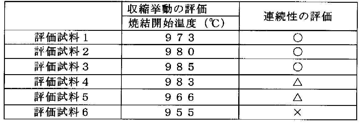
Claims (2)
- ニッケル粉末と、分散剤と、有機ビヒクルを主成分とする積層セラミックコンデンサの内部電極形成に用いるニッケルペーストであって、前記分散剤がリン酸ポリエステルを含有することを特徴とする積層セラミックコンデンサ用ニッケルペースト。
- 前記リン酸ポリエステルの含有量が、ニッケル粉末100質量部に対し、0.3質量部以上3質量部以下であることを特徴とする、請求項1に記載の積層セラミックコンデンサ用ニッケルペースト。
Priority Applications (4)
| Application Number | Priority Date | Filing Date | Title |
|---|---|---|---|
| KR1020217018390A KR102819416B1 (ko) | 2019-01-08 | 2019-01-08 | 적층 세라믹 콘덴서용 니켈 페이스트 |
| PCT/JP2019/000252 WO2020144746A1 (ja) | 2019-01-08 | 2019-01-08 | 積層セラミックコンデンサ用ニッケルペースト |
| MYPI2021002818A MY207997A (en) | 2019-01-08 | 2019-01-08 | Nickel paste for multilayer ceramic capacitors |
| CN201980088188.0A CN113272919A (zh) | 2019-01-08 | 2019-01-08 | 层叠陶瓷电容器用镍糊料 |
Applications Claiming Priority (1)
| Application Number | Priority Date | Filing Date | Title |
|---|---|---|---|
| PCT/JP2019/000252 WO2020144746A1 (ja) | 2019-01-08 | 2019-01-08 | 積層セラミックコンデンサ用ニッケルペースト |
Publications (1)
| Publication Number | Publication Date |
|---|---|
| WO2020144746A1 true WO2020144746A1 (ja) | 2020-07-16 |
Family
ID=71521499
Family Applications (1)
| Application Number | Title | Priority Date | Filing Date |
|---|---|---|---|
| PCT/JP2019/000252 Ceased WO2020144746A1 (ja) | 2019-01-08 | 2019-01-08 | 積層セラミックコンデンサ用ニッケルペースト |
Country Status (4)
| Country | Link |
|---|---|
| KR (1) | KR102819416B1 (ja) |
| CN (1) | CN113272919A (ja) |
| MY (1) | MY207997A (ja) |
| WO (1) | WO2020144746A1 (ja) |
Cited By (3)
| Publication number | Priority date | Publication date | Assignee | Title |
|---|---|---|---|---|
| WO2022114121A1 (ja) * | 2020-11-26 | 2022-06-02 | 住友金属鉱山株式会社 | 導電性ペースト及び積層セラミックコンデンサ |
| WO2024010075A1 (ja) * | 2022-07-08 | 2024-01-11 | 住友金属鉱山株式会社 | 導電性ペースト、乾燥膜、内部電極、及び、積層セラミックコンデンサ |
| JPWO2024209540A1 (ja) * | 2023-04-04 | 2024-10-10 |
Citations (9)
| Publication number | Priority date | Publication date | Assignee | Title |
|---|---|---|---|---|
| JPH01205410A (ja) * | 1988-02-10 | 1989-08-17 | Nippon Chemicon Corp | 積層セラミックコンデンサの製造方法 |
| JPH06172017A (ja) * | 1992-12-08 | 1994-06-21 | Unitika Ltd | セラミツクス基板用グリーンシート及びセラミツクス基板 |
| JP2004158397A (ja) * | 2001-12-21 | 2004-06-03 | Kawatetsu Mining Co Ltd | 分散性に優れた金属超微粉スラリー |
| JP2004263205A (ja) * | 2003-01-31 | 2004-09-24 | Toho Titanium Co Ltd | 金属微粉末およびその製造方法ならびにこの金属微粉末を用いた導電ペースト |
| JP2005298792A (ja) * | 2003-06-26 | 2005-10-27 | Sekisui Chem Co Ltd | 導電ペースト用バインダー樹脂及び導電ペースト |
| JP2006004905A (ja) * | 2004-03-10 | 2006-01-05 | Murata Mfg Co Ltd | 導電性ペーストおよびこれを用いたセラミック電子部品 |
| JP2007021475A (ja) * | 2005-07-15 | 2007-02-01 | Samsung Electro Mech Co Ltd | リン酸系分散剤、それを利用したペースト組成物及び分散方法 |
| JP2014111800A (ja) * | 2012-12-05 | 2014-06-19 | Nippon Handa Kk | ペースト状金属微粒子組成物、固形状金属または固形状金属合金の製造方法、金属製部材の接合方法、プリント配線板の製造方法および電気回路接続用バンプの製造方法 |
| JP2017182932A (ja) * | 2016-03-28 | 2017-10-05 | Jxtgエネルギー株式会社 | 金属粉ペーストの製造方法、金属粉ペーストのスクリーン印刷方法、電極の製造方法、チップ積層セラミックコンデンサーの製造方法および金属粉ペースト |
Family Cites Families (7)
| Publication number | Priority date | Publication date | Assignee | Title |
|---|---|---|---|---|
| JP4595613B2 (ja) | 2005-03-25 | 2010-12-08 | パナソニック株式会社 | 電極用ペーストならびにこれを用いた積層セラミック電子部品の製造方法 |
| JP4947418B2 (ja) * | 2007-04-27 | 2012-06-06 | 住友金属鉱山株式会社 | 導電性ペースト、導電性ペースト乾燥膜及びそれを用いた積層セラミックコンデンサ |
| JP5934336B2 (ja) * | 2011-03-29 | 2016-06-15 | サン ケミカル コーポレイション | ワックスチクソトロープ剤を含有する高いアスペクト比のスクリーン印刷可能な厚膜ペースト組成物 |
| JP5942791B2 (ja) | 2012-11-07 | 2016-06-29 | 住友金属鉱山株式会社 | ニッケル粉末の製造方法 |
| JP2015049973A (ja) | 2013-08-30 | 2015-03-16 | 新日鉄住金化学株式会社 | 導電性ペースト及びそれに用いる複合ニッケル微粒子の製造方法 |
| JP2017128782A (ja) * | 2016-01-22 | 2017-07-27 | 新日鉄住金化学株式会社 | ニッケル微粒子含有組成物及び接合材 |
| KR101893470B1 (ko) * | 2017-08-22 | 2018-08-30 | 한국화학연구원 | 3차원 프린팅을 위한 전극형성용 페이스트 조성물 및 이를 이용한 전극 |
-
2019
- 2019-01-08 WO PCT/JP2019/000252 patent/WO2020144746A1/ja not_active Ceased
- 2019-01-08 MY MYPI2021002818A patent/MY207997A/en unknown
- 2019-01-08 KR KR1020217018390A patent/KR102819416B1/ko active Active
- 2019-01-08 CN CN201980088188.0A patent/CN113272919A/zh active Pending
Patent Citations (9)
| Publication number | Priority date | Publication date | Assignee | Title |
|---|---|---|---|---|
| JPH01205410A (ja) * | 1988-02-10 | 1989-08-17 | Nippon Chemicon Corp | 積層セラミックコンデンサの製造方法 |
| JPH06172017A (ja) * | 1992-12-08 | 1994-06-21 | Unitika Ltd | セラミツクス基板用グリーンシート及びセラミツクス基板 |
| JP2004158397A (ja) * | 2001-12-21 | 2004-06-03 | Kawatetsu Mining Co Ltd | 分散性に優れた金属超微粉スラリー |
| JP2004263205A (ja) * | 2003-01-31 | 2004-09-24 | Toho Titanium Co Ltd | 金属微粉末およびその製造方法ならびにこの金属微粉末を用いた導電ペースト |
| JP2005298792A (ja) * | 2003-06-26 | 2005-10-27 | Sekisui Chem Co Ltd | 導電ペースト用バインダー樹脂及び導電ペースト |
| JP2006004905A (ja) * | 2004-03-10 | 2006-01-05 | Murata Mfg Co Ltd | 導電性ペーストおよびこれを用いたセラミック電子部品 |
| JP2007021475A (ja) * | 2005-07-15 | 2007-02-01 | Samsung Electro Mech Co Ltd | リン酸系分散剤、それを利用したペースト組成物及び分散方法 |
| JP2014111800A (ja) * | 2012-12-05 | 2014-06-19 | Nippon Handa Kk | ペースト状金属微粒子組成物、固形状金属または固形状金属合金の製造方法、金属製部材の接合方法、プリント配線板の製造方法および電気回路接続用バンプの製造方法 |
| JP2017182932A (ja) * | 2016-03-28 | 2017-10-05 | Jxtgエネルギー株式会社 | 金属粉ペーストの製造方法、金属粉ペーストのスクリーン印刷方法、電極の製造方法、チップ積層セラミックコンデンサーの製造方法および金属粉ペースト |
Cited By (7)
| Publication number | Priority date | Publication date | Assignee | Title |
|---|---|---|---|---|
| WO2022114121A1 (ja) * | 2020-11-26 | 2022-06-02 | 住友金属鉱山株式会社 | 導電性ペースト及び積層セラミックコンデンサ |
| JP2022084400A (ja) * | 2020-11-26 | 2022-06-07 | 住友金属鉱山株式会社 | 導電性ペースト及び積層セラミックコンデンサ |
| WO2024010075A1 (ja) * | 2022-07-08 | 2024-01-11 | 住友金属鉱山株式会社 | 導電性ペースト、乾燥膜、内部電極、及び、積層セラミックコンデンサ |
| JP2024008536A (ja) * | 2022-07-08 | 2024-01-19 | 住友金属鉱山株式会社 | 導電性ペースト、乾燥膜、内部電極、及び、積層セラミックコンデンサ |
| JP7831167B2 (ja) | 2022-07-08 | 2026-03-17 | 住友金属鉱山株式会社 | 導電性ペースト、乾燥膜、内部電極、及び、積層セラミックコンデンサ |
| JPWO2024209540A1 (ja) * | 2023-04-04 | 2024-10-10 | ||
| JP7819413B2 (ja) | 2023-04-04 | 2026-02-24 | 三菱電機株式会社 | 高周波パッケージおよび高周波パッケージの製造方法 |
Also Published As
| Publication number | Publication date |
|---|---|
| MY207997A (en) | 2025-04-03 |
| KR102819416B1 (ko) | 2025-06-11 |
| CN113272919A (zh) | 2021-08-17 |
| KR20210109531A (ko) | 2021-09-06 |
Similar Documents
| Publication | Publication Date | Title |
|---|---|---|
| JP5569747B2 (ja) | 積層セラミックコンデンサ内部電極に用いられるグラビア印刷用導電性ペースト | |
| JP2012174797A5 (ja) | ||
| CN102655052B (zh) | 电极烧结体、层压电子零件、内电极糊、电极烧结体的制备方法、层压电子零件的制备方法 | |
| CN114641835B (zh) | 层叠陶瓷电容器内部电极用导电膏组合物及其制造方法以及导电膏 | |
| JP6447903B2 (ja) | 積層セラミック電子部品用導電性ペーストの製造方法及びこの導電性ペーストを用いた積層セラミック電子部品の製造方法、並びにこの方法による積層セラミックコンデンサの製造方法 | |
| US11062847B2 (en) | Capacitor component and method for manufacturing the same | |
| JP7263694B2 (ja) | 積層セラミックコンデンサ用ニッケルペースト | |
| JP4947418B2 (ja) | 導電性ペースト、導電性ペースト乾燥膜及びそれを用いた積層セラミックコンデンサ | |
| KR102819416B1 (ko) | 적층 세라믹 콘덴서용 니켈 페이스트 | |
| CN103632742B (zh) | 用于内部电极的导电胶和使用该导电胶的多层陶瓷电子元件及其制造方法 | |
| US7744711B2 (en) | Manufacturing method of ceramic slurry, green sheet and multilayer ceramic device | |
| JP5887919B2 (ja) | 電極焼結体および積層電子部品 | |
| TWI795509B (zh) | 積層陶瓷電容器用鎳糊料 | |
| JP2007234330A (ja) | 導電体ペーストおよび電子部品 | |
| JP6152808B2 (ja) | 積層セラミックコンデンサ内部電極用導電性ペーストおよび積層セラミックコンデンサ | |
| JP2024146128A (ja) | 導電性ペースト、電子部品、及び、積層セラミックコンデンサ | |
| JP2024146126A (ja) | 導電性ペースト、電子部品、及び、積層セラミックコンデンサ | |
| JP2024146127A (ja) | 導電性ペースト、電子部品、及び、積層セラミックコンデンサ | |
| JP2013135096A (ja) | 電極焼結体、積層電子部品、内部電極ペースト、電極焼結体の製造方法、積層電子部品の製造方法 | |
| JP4517689B2 (ja) | 導電ペースト及びこれを用いた積層型電子部品 | |
| JP4088594B2 (ja) | 導電体ペースト、電子部品およびそれらの製造方法 | |
| JP5899912B2 (ja) | 電極焼結体、積層電子部品、内部電極ペースト、電極焼結体の製造方法、積層電子部品の製造方法 | |
| JP2007207885A (ja) | 積層セラミック電子部品 |
Legal Events
| Date | Code | Title | Description |
|---|---|---|---|
| 121 | Ep: the epo has been informed by wipo that ep was designated in this application |
Ref document number: 19909114 Country of ref document: EP Kind code of ref document: A1 |
|
| ENP | Entry into the national phase |
Ref document number: 20217018390 Country of ref document: KR Kind code of ref document: A |
|
| NENP | Non-entry into the national phase |
Ref country code: DE |
|
| 122 | Ep: pct application non-entry in european phase |
Ref document number: 19909114 Country of ref document: EP Kind code of ref document: A1 |
|
| NENP | Non-entry into the national phase |
Ref country code: JP |