WO2020138191A1 - 基板用コネクタ、及び機器 - Google Patents
基板用コネクタ、及び機器 Download PDFInfo
- Publication number
- WO2020138191A1 WO2020138191A1 PCT/JP2019/050875 JP2019050875W WO2020138191A1 WO 2020138191 A1 WO2020138191 A1 WO 2020138191A1 JP 2019050875 W JP2019050875 W JP 2019050875W WO 2020138191 A1 WO2020138191 A1 WO 2020138191A1
- Authority
- WO
- WIPO (PCT)
- Prior art keywords
- outer conductor
- connector
- board
- back wall
- circuit board
- Prior art date
Links
Images


Classifications
-
- H—ELECTRICITY
- H01—ELECTRIC ELEMENTS
- H01R—ELECTRICALLY-CONDUCTIVE CONNECTIONS; STRUCTURAL ASSOCIATIONS OF A PLURALITY OF MUTUALLY-INSULATED ELECTRICAL CONNECTING ELEMENTS; COUPLING DEVICES; CURRENT COLLECTORS
- H01R12/00—Structural associations of a plurality of mutually-insulated electrical connecting elements, specially adapted for printed circuits, e.g. printed circuit boards [PCB], flat or ribbon cables, or like generally planar structures, e.g. terminal strips, terminal blocks; Coupling devices specially adapted for printed circuits, flat or ribbon cables, or like generally planar structures; Terminals specially adapted for contact with, or insertion into, printed circuits, flat or ribbon cables, or like generally planar structures
- H01R12/70—Coupling devices
- H01R12/71—Coupling devices for rigid printing circuits or like structures
- H01R12/712—Coupling devices for rigid printing circuits or like structures co-operating with the surface of the printed circuit or with a coupling device exclusively provided on the surface of the printed circuit
- H01R12/716—Coupling device provided on the PCB
-
- H—ELECTRICITY
- H01—ELECTRIC ELEMENTS
- H01R—ELECTRICALLY-CONDUCTIVE CONNECTIONS; STRUCTURAL ASSOCIATIONS OF A PLURALITY OF MUTUALLY-INSULATED ELECTRICAL CONNECTING ELEMENTS; COUPLING DEVICES; CURRENT COLLECTORS
- H01R24/00—Two-part coupling devices, or either of their cooperating parts, characterised by their overall structure
- H01R24/38—Two-part coupling devices, or either of their cooperating parts, characterised by their overall structure having concentrically or coaxially arranged contacts
- H01R24/40—Two-part coupling devices, or either of their cooperating parts, characterised by their overall structure having concentrically or coaxially arranged contacts specially adapted for high frequency
- H01R24/50—Two-part coupling devices, or either of their cooperating parts, characterised by their overall structure having concentrically or coaxially arranged contacts specially adapted for high frequency mounted on a PCB [Printed Circuit Board]
-
- H—ELECTRICITY
- H01—ELECTRIC ELEMENTS
- H01R—ELECTRICALLY-CONDUCTIVE CONNECTIONS; STRUCTURAL ASSOCIATIONS OF A PLURALITY OF MUTUALLY-INSULATED ELECTRICAL CONNECTING ELEMENTS; COUPLING DEVICES; CURRENT COLLECTORS
- H01R13/00—Details of coupling devices of the kinds covered by groups H01R12/70 or H01R24/00 - H01R33/00
- H01R13/40—Securing contact members in or to a base or case; Insulating of contact members
- H01R13/42—Securing in a demountable manner
- H01R13/424—Securing in base or case composed of a plurality of insulating parts having at least one resilient insulating part
-
- H—ELECTRICITY
- H01—ELECTRIC ELEMENTS
- H01R—ELECTRICALLY-CONDUCTIVE CONNECTIONS; STRUCTURAL ASSOCIATIONS OF A PLURALITY OF MUTUALLY-INSULATED ELECTRICAL CONNECTING ELEMENTS; COUPLING DEVICES; CURRENT COLLECTORS
- H01R13/00—Details of coupling devices of the kinds covered by groups H01R12/70 or H01R24/00 - H01R33/00
- H01R13/46—Bases; Cases
- H01R13/502—Bases; Cases composed of different pieces
- H01R13/506—Bases; Cases composed of different pieces assembled by snap action of the parts
-
- H—ELECTRICITY
- H01—ELECTRIC ELEMENTS
- H01R—ELECTRICALLY-CONDUCTIVE CONNECTIONS; STRUCTURAL ASSOCIATIONS OF A PLURALITY OF MUTUALLY-INSULATED ELECTRICAL CONNECTING ELEMENTS; COUPLING DEVICES; CURRENT COLLECTORS
- H01R13/00—Details of coupling devices of the kinds covered by groups H01R12/70 or H01R24/00 - H01R33/00
- H01R13/62—Means for facilitating engagement or disengagement of coupling parts or for holding them in engagement
- H01R13/627—Snap or like fastening
- H01R13/6271—Latching means integral with the housing
- H01R13/6272—Latching means integral with the housing comprising a single latching arm
-
- H—ELECTRICITY
- H01—ELECTRIC ELEMENTS
- H01R—ELECTRICALLY-CONDUCTIVE CONNECTIONS; STRUCTURAL ASSOCIATIONS OF A PLURALITY OF MUTUALLY-INSULATED ELECTRICAL CONNECTING ELEMENTS; COUPLING DEVICES; CURRENT COLLECTORS
- H01R13/00—Details of coupling devices of the kinds covered by groups H01R12/70 or H01R24/00 - H01R33/00
- H01R13/648—Protective earth or shield arrangements on coupling devices, e.g. anti-static shielding
- H01R13/658—High frequency shielding arrangements, e.g. against EMI [Electro-Magnetic Interference] or EMP [Electro-Magnetic Pulse]
- H01R13/6591—Specific features or arrangements of connection of shield to conductive members
- H01R13/6594—Specific features or arrangements of connection of shield to conductive members the shield being mounted on a PCB and connected to conductive members
Definitions
- the technology disclosed in this specification relates to a technology related to a board connector arranged on a circuit board.
- This connector includes an inner conductor connected to a conductive path formed on a circuit board, an insulating dielectric surrounding the inner conductor, an outer conductor surrounding the dielectric, an inner conductor, and a dielectric. , And a connector housing in which the outer conductor is accommodated.
- the inner conductor connected to the conductive path of the circuit board is surrounded by the outer conductor, noise that enters the inner conductor from the outside of the board connector is suppressed, and the inner conductor leaks to the outside of the board connector. The noise that is generated is also suppressed.
- the above connector has a hood part to which the mating connector fits.
- a stopper to which the mating connector is locked is formed so as to project inward of the hood portion.
- a die-cutting hole for forming a stopper is penetrated through an inner wall provided on the side opposite to the open end of the hood portion. Therefore, there is a concern that noise generated from the circuit board may leak from the die-cutting hole of the connector housing to the outside of the board connector.
- the technology disclosed in this specification has been completed based on the above circumstances, and an object thereof is to provide a technology relating to a board connector having improved shield performance.
- the technology disclosed in the present specification is a board connector attached to a circuit board, which has a hood portion to which a mating connector fits and which is provided on the opposite side to the opening direction of the hood portion.
- a connector housing having a wall, an outer conductor inserted through an outer conductor mounting hole penetrating the inner wall, an insulating dielectric disposed inside the outer conductor, and an insulating dielectric disposed inside the dielectric.
- An inner conductor, and the outer conductor has a closing portion that closes a through hole formed at a position different from the outer conductor mounting hole in the inner wall.
- the through hole formed in the connector housing is closed by the closing portion of the outer conductor, so that noise generated from the circuit board may leak to the outside through the through hole of the board connector. Can be suppressed. As a result, the shield performance of the board connector can be improved.
- the noise generated from the circuit board includes noise generated from the conductive paths formed on the circuit board and also noise generated from the electronic components mounted on the circuit board.
- the outer conductor has a tubular portion that extends along the opening direction and accommodates at least a part of the inner conductor, and a flange protruding outward is provided on an outer periphery of the tubular portion.
- the closing portion is provided on the flange.
- the connector housing and the outer conductor can be easily aligned in the opening direction.
- the through hole in the back wall can be reliably closed.
- the connector housing and the outer conductor are positioned by the engaging projections provided on one of the inner wall and the flange and the engaging recesses provided on the other matingly.
- the connector housing and the outer conductor can be reliably positioned.
- the locking recess is provided in the flange, and the locking recess is provided on the small-diameter portion on the back wall side and on the side opposite to the back wall, and is formed larger in diameter than the small-diameter portion. And a large diameter portion, and the locking projection is filled in the locking recess.
- the locking convex portion filled in the locking concave portion is in contact with the boundary portion between the large diameter portion and the small diameter portion of the locking concave portion from the side opposite to the back wall,
- the connector housing and the flange are fixed.
- the positional displacement between the connector housing and the outer conductor can be suppressed, so that the shield performance of the board connector can be improved.
- the large-diameter portion has a tapered surface that expands in diameter with increasing distance from the inner wall.
- the locking projections filled in the locking recesses can easily come into close contact with the inner wall of the locking recesses. Thereby, the connector housing and the outer conductor can be more firmly fixed.
- the technology disclosed in the present specification is a device, and includes the above-mentioned board connector, a circuit board to which the board connector is attached, the circuit board, and the outer conductor and the electrical conductor. And a metal housing that are electrically connected to each other.
- the metal case is electrically connected to the outer conductor, it is possible to reliably suppress the noise generated from the circuit board housed in the case from leaking to the outside.
- the shield performance of the board connector can be improved.
- FIG. 5 is a perspective view showing the dielectric, which is viewed from an angle different from FIG. Perspective view showing board connector Front view showing board connector IX-IX line sectional view in FIG.
- FIG. 3 is a perspective view showing a board connector according to the second embodiment.
- FIG. 9 is a side view showing the board connector according to the third embodiment, showing the cross-sectional shapes of the locking projection and the locking recess.
- FIG. 11 is a side view showing the board connector according to the fourth embodiment, showing the cross-sectional shapes of the locking projection and the locking recess.
- FIG. 10 is a side view showing the board connector according to the fifth embodiment, showing the cross-sectional shapes of the locking projection and the locking recess.
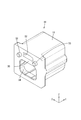
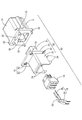
- the board connector 10 is attached to the circuit board 50 housed inside the device 60.
- the Z direction indicates the upper side
- the Y direction indicates the front side
- the X direction indicates the left side.
- only some of the members may be denoted by the reference numerals, and the reference numerals of the other members may be omitted.
- the device 60 includes a box-shaped lower case 61 that opens upward, and an upper case 62 that is assembled to the lower case 61 from above and closes the opening of the lower case 61.
- the lower case 61 and the upper case 62 are made of metal having conductivity.
- the casing 63 is formed by integrally assembling the lower case 61 and the upper case 62 by a known method such as screwing or locking.
- the housing 63 has a rectangular parallelepiped shape as a whole.
- a lower recess 64 that is recessed downward is formed at the upper edge of the front wall of the lower case 61.
- An upper concave portion 65 that is cut out upward is formed at a lower edge of a front wall of the upper case 62 at a position corresponding to the lower concave portion 64 of the lower case 61 in a state of being assembled to the lower case 61.
- the circuit board 50 is housed in the housing 63.
- the circuit board 50 is fixed to the housing 63 by a known method such as screwing.
- a signal conductive path 53 for transmitting a signal and a ground conductive path 54 are formed by a known printed wiring technique.
- a plurality of (four in this embodiment) through holes 51 for outer conductors and a plurality (two in this embodiment) through holes 52 for inner conductors are provided at positions near the front end of the circuit board 50.
- the circuit board 50 is formed so as to vertically pass therethrough.
- a conductive path (not shown) formed by plating or the like is formed on the inner surface of the outer conductor through hole 51 and the inner surface of the inner conductor through hole 52.
- the conductive path formed on the inner surface of the outer conductor through hole 51 is electrically connected to the ground conductive path 54.
- the conductive path formed on the inner surface of the inner conductor through hole 52 is electrically connected to the signal conductive path 53.
- Electronic components (not shown) are connected to the signal conductive path 53 and the ground conductive path 54 on the circuit board 50 by a known method such as soldering.
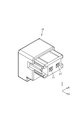
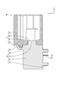
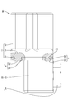
- the board connector 10 includes a connector housing 11 mounted on the circuit board 50, an outer conductor 20 mounted on the connector housing 11, and a dielectric 19 housed inside the outer conductor 20. And an inner conductor 18 housed inside the dielectric 19.
- the connector housing 11 is formed by injection molding an insulating synthetic resin.
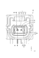
- the connector housing 11 is provided with a hood portion 15 that is open to the front (an example of the opening direction) and into which the mating connector 70 is fitted.
- a back wall 30 is provided on the opposite side of the connector housing 11 from the open end of the hood portion 15.
- a lock portion 31 protruding downward is formed at a front end edge (opening end portion) of the upper wall of the hood portion 15 so as to protrude downward. As shown in FIG. 2, the lock portion 31 engages with the lock arm 72 of the mating connector 70 fitted in the hood portion 15, whereby the mating connector 70 is held in the hood portion 15. ing.
- a die-cutting hole 32 (an example of a through hole) for forming the lock portion 31 when the connector housing 11 is injection-molded is provided at a position behind the lock portion 31 in the front-rear direction. Is formed so as to penetrate through.
- locking protrusions 33 projecting rearward are formed on both left and right sides of the die-cutting hole 32.
- the locking protrusion 33 is formed in a cylindrical shape (see FIG. 3).
- An outer conductor attachment hole 34 through which the outer conductor 20 is inserted, is formed in the inner wall 30 below the die-cutting hole 32 so as to penetrate the inner wall 30 in the front-rear direction.
- the cross section of the outer conductor mounting hole 34 has a rectangular shape with rounded corners.
- the outer conductor 20 is made of a conductive metal.
- any metal such as copper, copper alloy, aluminum, and aluminum alloy can be appropriately selected.
- the outer conductor 20 is formed by a known method such as casting, die casting, and cutting.
- the outer conductor 20 is adapted to make electrical contact with the mating outer conductor 73 housed in the mating connector 70 (see FIG. 2).
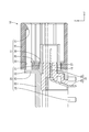
- the outer conductor 20 has a tubular portion 21 that extends in the front-rear direction and has a tubular shape, a dielectric surrounding portion 22 that extends rearward from a rear end edge of the tubular portion 21, and a boundary portion between the tubular portion 21 and the dielectric surrounding portion 22.
- the flange 23 protruding in a direction intersecting the front-back direction.
- Cylinder 21 has a rectangular cross section with rounded corners.
- the outer shape of the tubular portion 21 is set to be the same as or slightly smaller than the inner shape of the outer conductor mounting hole 34 of the inner wall 30. As a result, the tubular portion 21 is press-fitted into the outer conductor mounting hole 34.
- the dielectric surrounding portion 22 has a gate shape that opens downward when viewed from the rear.
- the dielectric 19 is housed inside the dielectric surrounding portion 22 in a state of being surrounded by the dielectric surrounding portion 22 on the upper side, the right side, and the left side.
- a plurality of (four in the present embodiment) substrate connecting portions 24 each having a columnar shape and protruding downward are provided at a lower end portion of the dielectric surrounding portion 22.
- the board connecting portion 24 is penetrated into the through hole 51 for the outer conductor of the circuit board 50 and is connected to the conductive path formed on the inner surface of the through hole 51 for the outer conductor by a known method such as soldering. As a result, the outer conductor 20 is electrically connected to the ground conductive path 54 formed on the circuit board 50.
- the flange 23 is adapted to come into contact with the rear surface of the inner wall 30 from the rear side in a state where the tubular portion 21 is press-fitted into the outer conductor mounting hole 34.
- a position of the flange 23 corresponding to the die-cutting hole 32 of the back wall 30 is a closing portion 25, which closes the die-cutting hole 32 from the rear side.
- the flange 23 is locked on both left and right sides of the closed portion 25 at positions corresponding to the locking protrusions 33 of the inner wall 30 so as to penetrate the flange 23 in the front-rear direction.
- a recess 26 is formed.
- the locking recess 26 has a circular cross section.
- the inner shape of the locking concave portion 26 is set to be substantially the same as the outer shape of the locking convex portion 33. The term “substantially the same” includes the case where they are the same, and includes the case where they can be recognized as substantially the same even if they are not the same.
- Dielectric 19 As shown in FIGS. 5 and 6, the dielectric 19 is formed by injection molding a synthetic resin product having an insulating property.
- the dielectric 19 is generally formed in an L-shaped cross section.
- the dielectric 19 includes an inner conductor housing chamber 27 that can house the inner conductor 18.
- the inner conductor accommodating chamber 27 is formed so as to penetrate the dielectric 19 in the front-rear direction and open on the lower surface side.
- the inner conductor 18 is formed by bending a tab-shaped metal plate in the middle, and a straight portion 28 extending in the front-rear direction (a direction along the plate surface of the circuit board 50) and a straight portion 28.
- the bent portion 29 is bent with respect to the portion 28 and extends in the up-down direction (direction orthogonal to the plate surface of the circuit board 50).
- the mating inner conductor 71 housed in the mating connector 70 can come into contact with the straight portion 28.
- the straight portion 28 projects forward of the dielectric 19.
- the bent portion 29 is bent downward at a right angle to the straight portion 28 and projects further downward from the lower surface of the connector housing 11.
- the protruding portion of the bent portion 29 from the lower surface of the connector housing 11 is inserted into the through hole 52 for the inner conductor formed in the circuit board 50 and is soldered to the signal formed on the circuit board 50. Is electrically connected to the conductive path 53.
- the tubular portion 21 of the outer conductor 20 is press-fitted from the rear into the outer conductor mounting hole 34 of the connector housing 11.
- the locking projection 33 is inserted into the locking recess 26 of the flange 23.
- the board connector 10 is assembled to the circuit board 50 from above.
- the board connecting portion 24 is inserted into the outer conductor through hole 51 of the circuit board 50 from above, and the lower end portion of the bent portion 29 is inserted into the inner conductor through hole 52 of the circuit board 50 from above. ..
- the lower ends of the board connecting portion 24 and the bent portion 29 are formed by soldering on the conductive paths formed on the inner surface of the outer conductor through hole 51 and the inner surface of the inner conductor through hole 52, respectively. Fixed to the conductive path.
- the upper case 62 is assembled from above the lower case 61, the lower case 61 and the upper case 62 are fixed, and the housing 63 is formed. At this time, the hole edge of the lower recess 64 provided in the lower case 61 is brought into contact with the outer surface of the outer conductor 20, and the hole edge of the upper recess 65 provided in the upper case 62 is brought into contact with the outer surface of the outer conductor 20. Let As a result, the outer conductor 20 and the housing 63 are electrically connected. With the above, the device 60 is completed.
- the lock arm 72 elastically deforms and elastically engages with the lock portion 31.
- the mating connector 70 is held in the connector housing 11 in a retaining state.
- the inner conductor 18 of the board connector 10 is electrically connected to the mating inner conductor 71 of the mating connector 70.
- the outer conductor 20 of the board connector 10 is electrically connected to the mating outer conductor 73 of the mating connector 70.
- the board connector 10 is a board connector 10 that is attached to a circuit board 50.
- the board connector 10 has a hood portion 15 into which a mating connector 70 fits, and an opening direction (arrow line) in which the hood portion 15 opens.
- Connector housing 11 having an inner wall 30 provided on the opposite side to the outer conductor 20, an outer conductor 20 provided in an outer conductor mounting hole 34 formed through the inner wall 30, and an outer conductor 20.
- an inner conductor 18 arranged inside the dielectric 19, and the outer conductor 20 is located at a position different from the outer conductor mounting hole 34 in the inner wall 30. It has a closing portion 25 that closes the formed die-cutting hole 32.
- the die-cutting hole 32 formed in the connector housing 11 is closed by the closing portion 25 of the outer conductor 20.
- noise generated from the signal conductive path 53 of the circuit board 50, the ground conductive path 54, the electronic components mounted on the circuit board 50, and the like leaks out from the die-cutting hole 32 of the board connector 10. Can be suppressed. Thereby, the shield performance of the board connector 10 can be improved.
- the outer conductor 20 has the tubular portion 21 that extends along the front-rear direction and that accommodates at least a part of the inner conductor 18, and the outer circumferential surface of the tubular portion 21 has an outer side.
- the flange 23 is provided so as to project to the bottom, and the flange 23 is provided with the closing portion 25.
- the connector housing 11 and the outer conductor 20 can be easily aligned in the front-rear direction of the hood portion 15.
- the die-cutting hole 32 of the back wall 30 can be reliably closed.
- the engaging projection 33 provided on the back wall 30 and the engaging recess 26 provided on the flange 23 are fitted in a concave-convex manner, whereby the connector housing 11 and the outer conductor 20 are connected. Is positioned.
- the connector housing 11 and the outer conductor 20 can be reliably positioned.
- the device 60 includes a board connector 10, a circuit board 50 to which the board connector 10 is attached, a metal board that accommodates the circuit board 50 and that is electrically connected to the outer conductor 20. And a housing 63 made of metal.
- the metal casing 63 is electrically connected to the outer conductor 20, it is ensured that noise generated from the circuit board 50 housed in the casing 63 leaks to the outside. Can be suppressed.
- the locking recess 83 formed in the flange 82 of the outer conductor 81 is a bottomed hole and does not penetrate the flange 82. This prevents the rear wall 30 of the rear surface of the rear wall 30 of the connector housing 11 where the flange 82 contacts from the rear from being exposed rearward.
- the noise generated from the circuit board 50 is electromagnetically shielded by the flange 82 of the outer conductor 81, so that the noise is suppressed from leaking to the outside from the inner wall 30 of the connector housing 11. It has become.
- the locking recess 91 provided in the flange 23 has a small diameter portion 92 located on the front side and a small diameter portion located on the rear side. And a large-diameter portion 93 having a larger diameter than 92.
- the locking projection 33 of the connector housing 11 has its rear end crushed by heating and pressurizing with the locking recess 91 being penetrated from the front to the rear.
- the crushed locking projection 33 has a small diameter portion 92 formed on the back wall 30 side of the connector housing 11 and a large diameter portion 93 provided on the opposite side of the back wall 30. It is filled inside.
- the locking projection 33 filled in the large-diameter portion 93 comes into contact with the boundary portion between the small-diameter portion 92 and the large-diameter portion 93 of the flange 82 from the rear side, whereby the connector housing 11 and the flange 23 are moved forward and backward. It is fixed in a state of being positioned in the direction.
- the crushed locking convex portion 33 comes into contact with the boundary portion between the large diameter portion 93 and the small diameter portion 92 of the locking concave portion 91 from the rear, whereby the connector housing 11 and the flange 23. And are fixed. Accordingly, the connector housing 11 and the outer conductor 20 can be fixed by a simple method of heat welding, so that the manufacturing work of the board connector 90 can be made efficient. Further, since the positional displacement between the connector housing 11 and the outer conductor 20 can be suppressed, the shield performance of the board connector 90 can be improved.
- a tapered surface 96 that increases in diameter from the front to the rear is formed at the front side of the large diameter portion 93 formed in the locking recess 95.
- the tapered surface 96 is formed so that the diameter thereof increases as the distance from the inner wall 30 of the connector housing 11 increases.
- the locking projection 33 of the connector housing 11 is penetrated into the locking recess 95 and then crushed by being heated and pressed to be filled in the locking recess 95.
- the tapered surface 96 is formed on the large-diameter portion 93, so that the molten and crushed locking convex portion 33 is easily brought into close contact with the inner wall of the locking concave portion 95. Thereby, the connector housing 11 and the outer conductor 20 can be more firmly fixed.
- all the inner surfaces of the large diameter portion 99 formed in the locking recess 98 are tapered surfaces 100 that increase in diameter from the front to the rear.
- the tapered surface 100 according to the present embodiment is also formed in a shape in which the diameter increases as the distance from the inner wall 30 of the connector housing 11 increases.
- the connector housing 11 and the outer conductor 20 can be more firmly fixed.
- the locking recess 26 may be provided on the back wall 30 and the locking projection 33 may be provided on the flange 23. Further, the locking convex portion 33 and the locking concave portion 26 may be omitted.
- the housing 63 may be made of synthetic resin.
- the outer conductor 20 may be formed by pressing a metal plate material.
- the number of the inner conductors 18 may be one, or may be three or more.
- the through hole formed in the inner wall 30 is not limited to the die-cutting hole 32 for injection-molding the lock portion 31, but includes a through hole formed for any purpose such as a drain hole and a vent hole.
- the closing portion 25 may be provided in a portion of the connector housing 11 different from the flange 23.
- the number of the locking protrusions 33 may be one, or may be three or more.
- the outer conductor is provided with the same number of locking recesses as the locking protrusions 33.
- Connector for board 11 Connector housing 15: Hood part 18: Inner conductor 19: Dielectric 20, 81: Outer conductor 21: Cylindrical part 22: Dielectric surrounding part 23, 82: Flange 24: Board connecting part 25: Closing part 26, 83, 91, 95, 98: Locking concave part 27: Inner conductor accommodating chamber 28: Straight part 29: Bending part 30: Back wall 31: Lock part 32: Die cutting hole ( (Example of through hole) 33: Locking convex portion 34: Outer conductor mounting hole 50: Circuit board 51: Through hole for outer conductor 52: Through hole for inner conductor 53: Conductive path for signal 54: Conductive path for ground 60: Equipment 61: Lower case 62: Upper case 63: Casing 64: Lower concave portion 65: Upper concave portion 70: Counter connector 71: Counter inner conductor 72: Lock arm 73: Counter outer conductor 92: Small diameter portion 93,99: Large diameter portion 96, 100: Taper surface
Abstract
回路基板50に取り付けられる基板用コネクタ10であって、相手方コネクタ70が嵌合するフード部15を有すると共に、フード部15が開口する開口方向と反対側に設けられた奥壁30を有するコネクタハウジング11と、奥壁30を貫通して形成された外導体取り付け孔34に配設された外導体20と、外導体20の内部に配された絶縁性の誘電体19と、誘電体19の内部に配された内導体18と、を備え、外導体20は、奥壁30のうち外導体取り付け孔34と異なる位置に形成された型抜き孔32を塞ぐ閉塞部25を有する。
Description
本明細書に開示された技術は、回路基板に配設される基板用コネクタに係る技術に関する。
従来、基板用コネクタとして、特開2008-59761号公報に記載のものが知られている。このコネクタは、回路基板に形成された導電路に接続される内導体と、内導体の周囲を包囲する絶縁性の誘電体と、誘電体の周囲を包囲する外導体と、内導体、誘電体、及び外導体が収容されるコネクタハウジングと、を備える。
回路基板の導電路に接続された内導体が外導体に包囲されていることにより、基板用コネクタの外部から内導体に侵入するノイズが抑制されると共に、内導体から基板用コネクタの外部に漏洩するノイズも抑制されるようになっている。
上記のコネクタは、相手方コネクタが嵌合するフード部を有する。フード部の開口端部には、相手方コネクタが係止されるストッパが、フード部の内方に突出して形成されている。フード部の開口端部と反対側に設けられた奥壁には、ストッパを形成するための型抜き孔が貫通されている。このため、回路基板から発生するノイズが、コネクタハウジングの型抜き孔から基板用コネクタの外部へと漏洩することが懸念される。
本明細書に開示された技術は上記のような事情に基づいて完成されたものであって、シールド性能が向上された基板用コネクタに関する技術を提供することを目的とする。
本明細書に開示された技術は、回路基板に取り付けられる基板用コネクタであって、相手方コネクタが嵌合するフード部を有すると共に、前記フード部が開口する開口方向と反対側に設けられた奥壁を有するコネクタハウジングと、前記奥壁を貫通する外導体取り付け孔に挿通された外導体と、前記外導体の内部に配された絶縁性の誘電体と、前記誘電体の内部に配された内導体と、を備え、前記外導体は、前記奥壁のうち前記外導体取り付け孔とは異なる位置に形成された貫通孔を塞ぐ閉塞部を有する。
上記の構成によれば、コネクタハウジングに形成された貫通孔は、外導体の閉塞部によって塞がれているので、回路基板から発生したノイズが、基板用コネクタの貫通孔から外部に漏洩することを抑制することができる。これにより、基板用コネクタのシールド性能を向上させることができる。回路基板から発生したノイズとは、回路基板に形成された導電路から発生したノイズを含むと共に、回路基板に実装された電子部品から発生したノイズも含む。
本明細書に開示された技術の実施態様としては以下の態様が好ましい。
前記外導体は、前記開口方向に沿って延びると共に、前記内導体の少なくも一部を収容する筒部を有し、前記筒部の外周には、外方に突出するフランジが設けられており、前記フランジに前記閉塞部が設けられている。
上記の構成によれば、コネクタハウジングの奥壁にフランジを接触させることにより、コネクタハウジングと外導体の、開口方向についての位置合わせを容易に行うことができる。
また、コネクタハウジングの奥壁とフランジとを接触させることにより、奥壁の貫通孔を確実に塞ぐことができる。
前記奥壁及び前記フランジの一方に設けられた係止凸部と、他方に設けられた係止凹部とが凹凸嵌合することにより、前記コネクタハウジングと前記外導体とが位置決めされている。
上記の構成によれば、コネクタハウジングと外導体とを確実に位置決めすることができる。
前記係止凹部は前記フランジに設けられており、前記係止凹部は、前記奥壁側の径小部と、前記奥壁と反対側に設けられるとともに前記径小部よりも径大に形成された径大部と、を有し、前記係止凸部は前記係止凹部内に充填されている。
上記の構成によれば、係止凹部内に充填された係止凸部が、係止凹部のうち径大部と径小部との境界部分に、奥壁と反対側から接触することにより、コネクタハウジングとフランジとが固定される。これにより、コネクタハウジングと外導体との位置ずれを抑制できるので、基板用コネクタのシールド性能を向上できる。
前記径大部は、前記奥壁から離れるにつれて拡径するテーパ面を有する。
径大部にテーパ面が形成されていることにより、係止凹部内に充填された係止凸部が、係止凹部の内壁に密着しやすくなっている。これにより、コネクタハウジングと外導体とをより強固に固定することができる。
また、本明細書に開示された技術は、機器であって、上記の基板用コネクタと、前記基板用コネクタが取り付けられた回路基板と、前記回路基板が収容されると共に、前記外導体と電気的に接続された金属製の筐体と、を備える。
上記の構成によれば、金属製の筐体が外導体と電気的に接続されているので、筐体に収容された回路基板から発生するノイズが外部に漏洩することを、確実に抑制することができる。
本明細書に開示された技術によれば、基板用コネクタのシールド性能を向上させることができる。
<実施形態1>
本明細書に開示された技術の実施形態1を図1から図9を参照しつつ説明する。本実施形態に係る基板用コネクタ10は、機器60の内部に収容された回路基板50に取り付けられる。以下の説明において、Z方向は上方を示し、Y方向は前方を示し、X方向は左方を示す。また、複数の同一部材については、一部の部材にのみ符号を付して、他の部材の符号を省略する場合がある。
本明細書に開示された技術の実施形態1を図1から図9を参照しつつ説明する。本実施形態に係る基板用コネクタ10は、機器60の内部に収容された回路基板50に取り付けられる。以下の説明において、Z方向は上方を示し、Y方向は前方を示し、X方向は左方を示す。また、複数の同一部材については、一部の部材にのみ符号を付して、他の部材の符号を省略する場合がある。
機器60
図1及び図2に示すように機器60は、上方に開口する箱状をなすロアケース61と、ロアケース61に上方から組み付けられてロアケース61の開口を塞ぐアッパーケース62と、を備える。ロアケース61とアッパーケース62は導電性を有する金属製である。ロアケース61とアッパーケース62とが、ネジ止め、ロック構造等の公知の手法により一体に組み付けられることにより、筐体63が形成される。筐体63は全体として直方体形状をなしている。
図1及び図2に示すように機器60は、上方に開口する箱状をなすロアケース61と、ロアケース61に上方から組み付けられてロアケース61の開口を塞ぐアッパーケース62と、を備える。ロアケース61とアッパーケース62は導電性を有する金属製である。ロアケース61とアッパーケース62とが、ネジ止め、ロック構造等の公知の手法により一体に組み付けられることにより、筐体63が形成される。筐体63は全体として直方体形状をなしている。
ロアケース61の前壁の上端縁には、下方に陥没した下側凹部64が形成されている。アッパーケース62の前壁の下端縁には、ロアケース61に組み付けられた状態で、ロアケース61の下側凹部64に対応する位置に、上方に切り欠かれた上側凹部65が形成されている。ロアケース61とアッパーケース62とが組み付けられた状態で、下側凹部64と上側凹部65とにより形成された空間内に、基板用コネクタ10が組み付けられるようになっている。
筐体63内には、回路基板50が収容されている。回路基板50は、ネジ止め等の公知の手法により、筐体63に固定されている。回路基板50には、公知のプリント配線技術により、信号が伝送される信号用導電路53と、グランド用導電路54と、が形成されている。回路基板50の前端部寄りの位置には、複数(本実施形態であは4つ)の外導体用スルーホール51と、複数(本実施形態では2つ)の内導体用スルーホール52とが、回路基板50を上下方向に貫通して形成されている。外導体用スルーホール51の内面、及び内導体用スルーホール52の内面には、メッキ等により形成された導電路(図示せず)が形成されている。外導体用スルーホール51の内面に形成された導電路は、グランド用導電路54と電気的に接続されている。また、内導体用スルーホール52の内面に形成された導電路は信号用導電路53と電気的に接続されている。回路基板50には、図示しない電子部品が半田付け等の公知の手法により、信号用導電路53、及びグランド用導電路54に接続されている。
基板用コネクタ10
図2に示すように、基板用コネクタ10は、回路基板50に取り付けられるコネクタハウジング11と、コネクタハウジング11に装着される外導体20と、外導体20の内部に収容される誘電体19と、誘電体19の内部に収容される内導体18と、を有する。
図2に示すように、基板用コネクタ10は、回路基板50に取り付けられるコネクタハウジング11と、コネクタハウジング11に装着される外導体20と、外導体20の内部に収容される誘電体19と、誘電体19の内部に収容される内導体18と、を有する。
コネクタハウジング11
図3及び図9に示すように、コネクタハウジング11は、絶縁性の合成樹脂を射出成型することにより形成される。コネクタハウジング11は、前方(開口方向の一例)に開口すると共に、相手方コネクタ70が内嵌されるフード部15を備える。コネクタハウジング11のうち、フード部15の開口端部と反対側には奥壁30が設けられている。フード部15の上壁の前端縁(開口端部)には、下方に突出するロック部31が下方に突出して形成されている。図2に示すように、ロック部31が、フード部15内に内嵌された相手方コネクタ70のロックアーム72と係合することにより、相手方コネクタ70がフード部15内に保持されるようになっている。
図3及び図9に示すように、コネクタハウジング11は、絶縁性の合成樹脂を射出成型することにより形成される。コネクタハウジング11は、前方(開口方向の一例)に開口すると共に、相手方コネクタ70が内嵌されるフード部15を備える。コネクタハウジング11のうち、フード部15の開口端部と反対側には奥壁30が設けられている。フード部15の上壁の前端縁(開口端部)には、下方に突出するロック部31が下方に突出して形成されている。図2に示すように、ロック部31が、フード部15内に内嵌された相手方コネクタ70のロックアーム72と係合することにより、相手方コネクタ70がフード部15内に保持されるようになっている。
奥壁30には、ロック部31の後方の位置に、コネクタハウジング11を射出成型する際にロック部31を形成するための型抜き孔32(貫通孔の一例)が、前後方向に奥壁30を貫通して形成されている。奥壁30の外面には、型抜き孔32の左右両側方に、後方に突出する係止凸部33が形成されている。係止凸部33は円柱状に形成されている(図3参照)。
奥壁30には、型抜き孔32の下方に、外導体20が挿通される外導体取り付け孔34が、前後方向に奥壁30を貫通して形成されている。外導体取り付け孔34の断面形状は、角が丸められた長方形状をなしている。
外導体20
図4に示すように、外導体20は、導電性を有する金属製である。外導体20を構成する金属としては、銅、銅合金、アルミニウム、アルミニウム合金等、任意の金属を適宜に選択できる。外導体20は、鋳造、ダイキャスト、切削加工等、公知の手法により形成される。外導体20は、相手方コネクタ70に収容された相手方外導体73と電気的に接触するようになっている(図2参照)。
図4に示すように、外導体20は、導電性を有する金属製である。外導体20を構成する金属としては、銅、銅合金、アルミニウム、アルミニウム合金等、任意の金属を適宜に選択できる。外導体20は、鋳造、ダイキャスト、切削加工等、公知の手法により形成される。外導体20は、相手方コネクタ70に収容された相手方外導体73と電気的に接触するようになっている(図2参照)。
外導体20は、前後方向に延びると共に筒状をなす筒部21と、筒部21の後端縁から後方に延びる誘電体包囲部22と、筒部21と誘電体包囲部22との境界部分において、前後方向と交差する方向に突出するフランジ23と、を有する。
筒部21の断面形状は、角が丸められた長方形状をなしている。筒部21の外形状は、奥壁30の外導体取り付け孔34の内形状と同じか、やや小さく設定されている。これにより、筒部21は、外導体取り付け孔34内に圧入されるようになっている。
誘電体包囲部22は、後方から見て、下方に開口した門形状をなしている。誘電体包囲部22の内部には、誘電体19が、誘電体包囲部22によって、上方、右方、及び左方を包囲された状態で、収容されるようになっている。
誘電体包囲部22の下端部には、下方に突出する円柱状をなす複数(本実施形態では4つ)の基板接続部24が設けられている。基板接続部24は、回路基板50の外導体用スルーホール51内に貫通されて、はんだ付け等の公知の手法により、外導体用スルーホール51の内面に形成された導電路と接続される。これにより、外導体20は回路基板50に形成されたグランド用導電路54と電気的に接続される。
図9に示すように、筒部21が外導体取り付け孔34内に圧入された状態で、フランジ23は、奥壁30の後面に後方から接触するようになっている。フランジ23のうち、奥壁30の型抜き孔32に対応する位置は、閉塞部25とされ、型抜き孔32を後方から塞ぐようになっている。
図7に示すように、フランジ23には、閉塞部25の左右両側方であって、奥壁30の係止凸部33に対応する位置に、それぞれ、フランジ23を前後方向に貫通する係止凹部26が形成されている。係止凹部26の断面形状は円形状をなしている。係止凹部26の内形状は、係止凸部33の外形状と、略同じに設定されている。略同じとは、同じである場合を含むと共に、同じでない場合であっても、実質的に同じと認定しうる場合も含む。
誘電体19
図5及び図6に示すように、誘電体19は、絶縁性を有する合成樹脂製を射出成型してなる。誘電体19は、概ね、断面L字型に形成されている。誘電体19は、内部に内導体18を収容可能な内導体収容室27を備える。内導体収容室27は、誘電体19を前後に貫通するとともに、下面側にも開口して形成されている。
図5及び図6に示すように、誘電体19は、絶縁性を有する合成樹脂製を射出成型してなる。誘電体19は、概ね、断面L字型に形成されている。誘電体19は、内部に内導体18を収容可能な内導体収容室27を備える。内導体収容室27は、誘電体19を前後に貫通するとともに、下面側にも開口して形成されている。
内導体18
図9に示すように、内導体18は、タブ状の金属板を途中で屈曲させることで形成され、前後方向(回路基板50の板面に沿う方向)に沿って延びるストレート部28と、ストレート部28に対して屈曲されて上下方向(回路基板50の板面と直交する方向)に沿って延びる屈曲部29とを備える。
図9に示すように、内導体18は、タブ状の金属板を途中で屈曲させることで形成され、前後方向(回路基板50の板面に沿う方向)に沿って延びるストレート部28と、ストレート部28に対して屈曲されて上下方向(回路基板50の板面と直交する方向)に沿って延びる屈曲部29とを備える。
図2に示すように、ストレート部28には、相手方コネクタ70に収容された相手方内導体71が接触可能になっている。ストレート部28は、誘電体19よりも前方へ突き出している。一方、屈曲部29は、ストレート部28に対して下向きにほぼ直角に曲げられて、コネクタハウジング11の下面からさらに下方へ突出している。屈曲部29のうちコネクタハウジング11の下面からの突出部分が、回路基板50に形成された内導体用スルーホール52に対して差し込まれるとともに半田付けされることで、回路基板50に形成された信号用導電路53に対して電気的に接続される。
続いて、本実施形態に係る基板用コネクタ10及び機器60の組み立て工程の一例について説明する。基板用コネクタ10及び機器60の組み立て工程は、以下の記載に限定されない。
誘電体19の内導体収容室27内に、後方から内導体18を挿入する。続いて、内導体18を外導体20に対して、後方から組み付ける。これにより、誘電体19のうち前後方向に延びる部分が、外導体20の筒部21の内部に圧入される。
続いて、コネクタハウジング11の外導体取り付け孔34に、外導体20の筒部21を後方から圧入する。このとき、フランジ23の係止凹部26内に、係止凸部33が挿入されるようにする。上記の工程により、基板用コネクタ10が完成する。
次に、回路基板50に対して、上方から基板用コネクタ10を組み付ける。回路基板50の外導体用スルーホール51に対して、上方から基板接続部24を挿入すると共に、回路基板50の内導体用スルーホール52に対して、上方から屈曲部29の下端部を挿入する。その後、基板接続部24、及び屈曲部29の下端部を、はんだ付けにより、それぞれ、外導体用スルーホール51の内面に形成された導電路、及び、内導体用スルーホール52の内面に形成された導電路に固定する。
回路基板50をロアケース61に固定する。ロアケース61の上方からアッパーケース62を組み付けて、ロアケース61とアッパーケース62とを固定し、筐体63を形成する。このとき、ロアケース61に設けられた下側凹部64の孔縁部を外導体20の外面に接触させると共に、アッパーケース62に設けられた上側凹部65の孔縁部を外導体20の外面に接触させる。これにより、外導体20と、筐体63とが電気的に接続される。以上により、機器60が完成する。
フード部15内に、前方から相手方コネクタ70を嵌入させる。ロックアーム72が弾性変形し、ロック部31と弾性的に係合する。これにより、相手方コネクタ70が、コネクタハウジング11に抜け止め状態で保持される。この状態で、基板用コネクタ10の内導体18は、相手方コネクタ70の相手方内導体71と電気的に接続される。また、基板用コネクタ10の外導体20は、相手方コネクタ70の相手方外導体73と電気的に接続される。
続いて、本実施形態の作用効果について説明する。本実施形態に係る基板用コネクタ10は、回路基板50に取り付けられる基板用コネクタ10であって、相手方コネクタ70が嵌合するフード部15を有すると共に、フード部15が開口する開口方向(矢線Aで示す方向)と反対側に設けられた奥壁30を有するコネクタハウジング11と、奥壁30を貫通して形成された外導体取り付け孔34に配設された外導体20と、外導体20の内部に配された絶縁性の誘電体19と、誘電体19の内部に配された内導体18と、を備え、外導体20は、奥壁30のうち外導体取り付け孔34と異なる位置に形成された型抜き孔32を塞ぐ閉塞部25を有する。
上記の構成によれば、コネクタハウジング11に形成された型抜き孔32は、外導体20の閉塞部25によって塞がれている。これにより、回路基板50の信号用導電路53、グランド用導電路54、及び回路基板50に実装された電子部品等から発生したノイズが、基板用コネクタ10の型抜き孔32から外部に漏洩することを抑制することができる。これにより、基板用コネクタ10のシールド性能を向上させることができる。
また、本実施形態によれば、外導体20は、前後方向に沿って延びると共に、内導体18の少なくも一部を収容する筒部21を有し、筒部21の外周には、外方に突出するフランジ23が設けられており、フランジ23に閉塞部25が設けられている。
上記の構成によれば、コネクタハウジング11の奥壁30にフランジ23を接触させることにより、コネクタハウジング11と外導体20の、フード部15の前後方向についての位置合わせを容易に行うことができる。
また、コネクタハウジング11の奥壁30とフランジ23とを接触させることにより、奥壁30の型抜き孔32を確実に塞ぐことができる。
また、本実施形態によれば、奥壁30に設けられた係止凸部33と、フランジ23に設けられた係止凹部26とが凹凸嵌合することにより、コネクタハウジング11と外導体20とが位置決めされている。
上記の構成によれば、コネクタハウジング11と外導体20とを確実に位置決めすることができる。
また、本実施形態に係る機器60は、基板用コネクタ10と、基板用コネクタ10が取り付けられた回路基板50と、回路基板50が収容されると共に、外導体20と電気的に接続された金属製の筐体63と、を備えている。
上記の構成によれば、金属製の筐体63が外導体20と電気的に接続されているので、筐体63に収容された回路基板50から発生するノイズが外部に漏洩することを、確実に抑制することができる。
<実施形態2>
本明細書に開示された技術の実施形態2を図10から図11を参照しつつ説明する。この実施形態2に係る基板用コネクタ80では、外導体81のフランジ82に形成された係止凹部83は有底孔であって、フランジ82を貫通していない。これにより、コネクタハウジング11の奥壁30の後面のうち、フランジ82が後方から接触した部分については、奥壁30が後方に露出しないようになっている。
本明細書に開示された技術の実施形態2を図10から図11を参照しつつ説明する。この実施形態2に係る基板用コネクタ80では、外導体81のフランジ82に形成された係止凹部83は有底孔であって、フランジ82を貫通していない。これにより、コネクタハウジング11の奥壁30の後面のうち、フランジ82が後方から接触した部分については、奥壁30が後方に露出しないようになっている。
上記以外の構成については、実施形態1と略同様なので、同一部材については同一符号を付し、重複する説明を省略する。
本実施形態によれば、回路基板50から発生したノイズは、外導体81のフランジ82によって電磁的にシールドされることにより、コネクタハウジング11の奥壁30から外部に漏洩することが抑制されるようになっている。
<実施形態3>
本明細書に開示された技術の実施形態3について、図12から図14を参照しつつ説明する。図12に示されるように、実施形態3にかかる基板用コネクタ90において、フランジ23に設けられた係止凹部91は、前側に位置する径小部92と、後側に位置するとともに径小部92よりも径大な径大部93とを有する。
本明細書に開示された技術の実施形態3について、図12から図14を参照しつつ説明する。図12に示されるように、実施形態3にかかる基板用コネクタ90において、フランジ23に設けられた係止凹部91は、前側に位置する径小部92と、後側に位置するとともに径小部92よりも径大な径大部93とを有する。
図13に示されるように、コネクタハウジング11の係止凸部33は、係止凹部91内に、前方から後方に貫通された状態で、後端部が加熱および加圧によりつぶされている。
図14に示されるように、つぶされた係止凸部33は、コネクタハウジング11の奥壁30側に形成された径小部92と、奥壁30と反対側に設けられた径大部93内に充填された状態になっている。径大部93内に充填された係止凸部33が、フランジ82のうち径小部92と径大部93との境界部分に後方から接触することにより、コネクタハウジング11とフランジ23とが前後方向について位置決めされた状態で固定されている。
上記以外の構成については、実施形態1と略同様なので、同一部材については同一符号を付し、重複する説明を省略する。
上記の構成によれば、つぶされた係止凸部33が、係止凹部91のうち径大部93と径小部92との境界部分に後方から接触することにより、コネクタハウジング11とフランジ23とが固定される。これにより、熱溶着という簡易な手法によりコネクタハウジング11と外導体20とを固定できるので、基板用コネクタ90の製造作業を効率化することができる。また、コネクタハウジング11と外導体20との位置ずれを抑制できるので、基板用コネクタ90のシールド性能を向上できる。
<実施形態4>
本明細書に開示された技術の実施形態4について、図15を参照しつつ説明する。本実施形態にかかる基板用コネクタ94においては、係止凹部95に形成された径大部93の前側の部分に、前方から後方に向かうに従って拡径するテーパ面96が形成されている。換言すると、テーパ面96は、コネクタハウジング11の奥壁30から離れるに従って拡径するように形成されている。
本明細書に開示された技術の実施形態4について、図15を参照しつつ説明する。本実施形態にかかる基板用コネクタ94においては、係止凹部95に形成された径大部93の前側の部分に、前方から後方に向かうに従って拡径するテーパ面96が形成されている。換言すると、テーパ面96は、コネクタハウジング11の奥壁30から離れるに従って拡径するように形成されている。
コネクタハウジング11の係止凸部33は、係止凹部95内に貫通された後に、加熱、加圧されることによりつぶされて、係止凹部95内に充填された状態になっている。
上記以外の構成については、実施形態1と略同様なので、同一部材については同一符号を付し、重複する説明を省略する。
本実施形態においては、径大部93にテーパ面96が形成されていることにより、溶融、圧潰された係止凸部33が、係止凹部95の内壁に密着しやすくなっている。これにより、コネクタハウジング11と外導体20とをより強固に固定することができる。
<実施形態5>
本明細書に開示された技術の実施形態5について、図16を参照しつつ説明する。本実施形態にかかる基板用コネクタ97においては、係止凹部98に形成された径大部99の内面は、全て、前方から後方に向かうに従って拡径するテーパ面100とされる。本実施形態にかかるテーパ面100も、コネクタハウジング11の奥壁30から離れるに従って拡径する形状に形成されている。
本明細書に開示された技術の実施形態5について、図16を参照しつつ説明する。本実施形態にかかる基板用コネクタ97においては、係止凹部98に形成された径大部99の内面は、全て、前方から後方に向かうに従って拡径するテーパ面100とされる。本実施形態にかかるテーパ面100も、コネクタハウジング11の奥壁30から離れるに従って拡径する形状に形成されている。
上記以外の構成については、実施形態1と略同様なので、同一部材については同一符号を付し、重複する説明を省略する。
本実施形態によれば、径大部99の内面が全てテーパ面100とされているので、溶融、圧潰された係止凸部33が、係止凹部98の内壁により密着しやすくなっている。これにより、コネクタハウジング11と外導体20とをさらに強固に固定することができる。
<他の実施形態>
本明細書に開示された技術は上記記述及び図面によって説明した実施形態に限定されるものではなく、例えば次のような実施形態も本明細書に開示された技術の技術的範囲に含まれる。
本明細書に開示された技術は上記記述及び図面によって説明した実施形態に限定されるものではなく、例えば次のような実施形態も本明細書に開示された技術の技術的範囲に含まれる。
(1)奥壁30に係止凹部26が設けられ、フランジ23に係止凸部33が設けられる構成としてもよい。また、係止凸部33と、係止凹部26は省略してもよい。
(2)筐体63は、合成樹脂製であってもよい。
(3)外導体20は、金属板材をプレス加工することにより形成される構成としてもよい。
(4)内導体18は、1つでもよく、また、3つ以上の複数であってもよい。
(5)奥壁30に形成された貫通孔は、ロック部31を射出成型するための型抜き孔32に限られず、排水孔、通気孔等、任意の目的で形成された貫通孔を含む。
(6)閉塞部25は、コネクタハウジング11のうち、フランジ23と異なる部位に設けられる構成としてもよい。
(7)係止凸部33の個数は1つでもよく、また、3つ以上でもよい。外導体には、係止凸部33と同数の係止凹部が設けられる。
10,80,90,94,97:基板用コネクタ
11:コネクタハウジング
15:フード部
18:内導体
19:誘電体
20,81:外導体
21:筒部
22:誘電体包囲部
23,82:フランジ
24:基板接続部
25:閉塞部
26,83,91,95,98:係止凹部
27:内導体収容室
28:ストレート部
29:屈曲部
30:奥壁
31:ロック部
32:型抜き孔(貫通孔の一例)
33:係止凸部
34:外導体取り付け孔
50:回路基板
51:外導体用スルーホール
52:内導体用スルーホール
53:信号用導電路
54:グランド用導電路
60:機器
61:ロアケース
62:アッパーケース
63:筐体
64:下側凹部
65:上側凹部
70:相手方コネクタ
71:相手方内導体
72:ロックアーム
73:相手方外導体
92:径小部
93,99:径大部
96,100:テーパ面
Claims (6)
- 回路基板に取り付けられる基板用コネクタであって、
相手方コネクタが嵌合するフード部を有すると共に、前記フード部が開口する開口方向と反対側に設けられた奥壁を有するコネクタハウジングと、
前記奥壁を貫通する外導体取り付け孔に挿通された外導体と、
前記外導体の内部に配された絶縁性の誘電体と、
前記誘電体の内部に配された内導体と、を備え、
前記外導体は、前記奥壁のうち前記外導体取り付け孔とは異なる位置に形成された貫通孔を塞ぐ閉塞部を有する、基板用コネクタ。 - 前記外導体は、前記開口方向に沿って延びると共に、前記内導体の少なくも一部を収容する筒部を有し、
前記筒部の外周には、外方に突出するフランジが設けられており、前記フランジに前記閉塞部が設けられている、請求項1に記載の基板用コネクタ。 - 前記奥壁及び前記フランジの一方に設けられた係止凸部と、他方に設けられた係止凹部とが凹凸嵌合することにより、前記コネクタハウジングと前記外導体とが位置決めされている、請求項2に記載の基板用コネクタ。
- 前記係止凹部は前記フランジに設けられており、
前記係止凹部は、前記奥壁側の径小部と、前記奥壁と反対側に設けられるとともに前記径小部よりも径大に形成された径大部と、を有し、
前記係止凸部は前記係止凹部内に充填されている請求項3に記載の基板用コネクタ。 - 前記径大部は、前記奥壁から離れるにつれて拡径するテーパ面を有する請求項4に記載の基板用コネクタ。
- 請求項1から請求項5のいずれか一項に記載の基板用コネクタと、
前記基板用コネクタが取り付けられた回路基板と、
前記回路基板が収容されると共に、前記外導体と電気的に接続された金属製の筐体と、を備えた機器。
Priority Applications (2)
| Application Number | Priority Date | Filing Date | Title |
|---|---|---|---|
| US17/418,535 US11837808B2 (en) | 2018-12-28 | 2019-12-25 | Board connector and device |
| CN201980085465.2A CN113228423B (zh) | 2018-12-28 | 2019-12-25 | 基板用连接器及机器 |
Applications Claiming Priority (4)
| Application Number | Priority Date | Filing Date | Title |
|---|---|---|---|
| JP2018247604 | 2018-12-28 | ||
| JP2018-247604 | 2018-12-28 | ||
| JP2019-143489 | 2019-08-05 | ||
| JP2019143489A JP7228117B2 (ja) | 2018-12-28 | 2019-08-05 | 基板用コネクタ、及び機器 |
Publications (1)
| Publication Number | Publication Date |
|---|---|
| WO2020138191A1 true WO2020138191A1 (ja) | 2020-07-02 |
Family
ID=71129457
Family Applications (1)
| Application Number | Title | Priority Date | Filing Date |
|---|---|---|---|
| PCT/JP2019/050875 WO2020138191A1 (ja) | 2018-12-28 | 2019-12-25 | 基板用コネクタ、及び機器 |
Country Status (2)
| Country | Link |
|---|---|
| US (1) | US11837808B2 (ja) |
| WO (1) | WO2020138191A1 (ja) |
Citations (4)
| Publication number | Priority date | Publication date | Assignee | Title |
|---|---|---|---|---|
| JPH0523461U (ja) * | 1991-09-03 | 1993-03-26 | 富士通テン株式会社 | ジヤツクの取付構造 |
| JP2009066858A (ja) * | 2007-09-12 | 2009-04-02 | Sumitomo Wiring Syst Ltd | 樹脂成形品、樹脂成形品の成形方法、及び成形用金型 |
| JP2009277544A (ja) * | 2008-05-15 | 2009-11-26 | Sumitomo Wiring Syst Ltd | 基板用シールドコネクタ |
| JP2016143648A (ja) * | 2015-02-05 | 2016-08-08 | 株式会社オートネットワーク技術研究所 | シールドコネクタ |
Family Cites Families (42)
| Publication number | Priority date | Publication date | Assignee | Title |
|---|---|---|---|---|
| US4889503A (en) * | 1984-01-16 | 1989-12-26 | Stewart Stamping Corporation | Shielded plug and jack connector |
| JPS60183380U (ja) * | 1984-05-17 | 1985-12-05 | アムプ インコ−ポレ−テッド | 電気接続子ハウジング |
| JP2793380B2 (ja) * | 1991-06-17 | 1998-09-03 | 富士通株式会社 | 同軸マルチ混在コネクタ |
| US5244412A (en) * | 1991-12-24 | 1993-09-14 | Stewart Connector Systems, Inc. | Electrical device for surface mounting on a circuit board and mounting component thereof |
| US5234353A (en) * | 1992-03-03 | 1993-08-10 | Amp Incorporated | Hybrid input/output connector having low mating force and high cycle life and contacts therefor |
| US5344335A (en) * | 1992-03-03 | 1994-09-06 | The Whitaker Corporation | Latching system for electrical connectors |
| JP2836500B2 (ja) * | 1994-09-16 | 1998-12-14 | 住友電装株式会社 | 基板用コネクタ |
| US5913703A (en) * | 1996-04-24 | 1999-06-22 | Sumitomo Wiring Systems, Ltd. | Connector assembly with sequentially engageable housings |
| JP2001015223A (ja) * | 1999-06-25 | 2001-01-19 | Nec Corp | 汎用コネクタおよびその結合方法 |
| JP4226737B2 (ja) * | 1999-08-03 | 2009-02-18 | 日本圧着端子製造株式会社 | フラットケーブル用コネクタ及びその製造方法 |
| JP2001267000A (ja) * | 2000-03-21 | 2001-09-28 | Sumitomo Wiring Syst Ltd | 防水コネクタ |
| EP1337009B1 (en) * | 2002-02-15 | 2005-05-04 | Sumitomo Wiring Systems, Ltd. | A shielding connector, a shielding connector system, a terminal fitting and use thereof |
| DE10317154B4 (de) * | 2002-04-15 | 2009-03-26 | Yazaki Corp. | Verriegelungsaufbau für Steckverbinder |
| JP4028316B2 (ja) * | 2002-07-30 | 2007-12-26 | 矢崎総業株式会社 | コネクタ |
| JP4550470B2 (ja) * | 2004-04-14 | 2010-09-22 | 住友電装株式会社 | コネクタ |
| US7303438B2 (en) * | 2004-12-17 | 2007-12-04 | Molex Incorporated | Plug connector with mating protection and alignment means |
| JP2006294386A (ja) * | 2005-04-08 | 2006-10-26 | Tyco Electronics Amp Kk | 電気コネクタ、ワイヤハーネス及びワイヤハーネスの配置方法 |
| JP4828311B2 (ja) * | 2006-06-02 | 2011-11-30 | タイコエレクトロニクスジャパン合同会社 | 電気コネクタ |
| JP2008059761A (ja) | 2006-08-29 | 2008-03-13 | Auto Network Gijutsu Kenkyusho:Kk | 基板用シールドコネクタおよび基板用シールドコネクタの固定構造 |
| CN201204304Y (zh) * | 2008-04-25 | 2009-03-04 | 富士康(昆山)电脑接插件有限公司 | 电连接器 |
| JP5673320B2 (ja) * | 2011-04-18 | 2015-02-18 | 株式会社オートネットワーク技術研究所 | コネクタ |
| US9209540B2 (en) * | 2013-02-08 | 2015-12-08 | Apple Inc. | Board-to-board connectors |
| JP2015032433A (ja) * | 2013-08-01 | 2015-02-16 | ヒロセ電機株式会社 | 中継電気コネクタ |
| CN106030925A (zh) * | 2013-12-23 | 2016-10-12 | 富加宜(亚洲)私人有限公司 | 电连接器 |
| US9257767B2 (en) * | 2014-01-18 | 2016-02-09 | Advanced Micro Devices, Inc. | Connector adaptor to facilitate coupling of a mating card edge with a female card-edge connector |
| US9954306B2 (en) * | 2014-01-31 | 2018-04-24 | Panasonic Intellectual Property Management Co., Ltd. | Connector and connector device |
| US9525246B2 (en) * | 2014-05-05 | 2016-12-20 | Tyco Electronics Corporation | Printed circuit board connector assembly having contact shield with integral securing members |
| JP6252417B2 (ja) * | 2014-09-19 | 2017-12-27 | 株式会社オートネットワーク技術研究所 | コネクタ |
| CN112086780B (zh) * | 2014-10-23 | 2022-11-01 | 安费诺富加宜(亚洲)私人有限公司 | 夹层式电连接器 |
| GB2533354B (en) * | 2014-12-17 | 2017-09-13 | Etl Systems Ltd | Connector assembly and related methods and assemblies |
| TWI635675B (zh) * | 2015-11-06 | 2018-09-11 | 莫仕有限公司 | Plug connector assembly |
| WO2017125314A1 (en) * | 2016-01-18 | 2017-07-27 | Huber+Suhner Ag | Highspeed board connector |
| JP6627599B2 (ja) * | 2016-03-23 | 2020-01-08 | 株式会社オートネットワーク技術研究所 | 基板用防水コネクタ及び基板付きコネクタ |
| JP6745125B2 (ja) * | 2016-03-29 | 2020-08-26 | 株式会社堀場エステック | 流体制御装置 |
| US10673173B2 (en) * | 2016-05-24 | 2020-06-02 | Nippon Tanshi Co., Ltd. | Connector structure |
| JP6797677B2 (ja) * | 2016-12-28 | 2020-12-09 | 株式会社フジクラ | 電気コネクタ |
| DE102017100538B3 (de) * | 2017-01-12 | 2018-05-09 | Knorr-Bremse Systeme für Nutzfahrzeuge GmbH | Elektrische Steckverbindung aus einem Stecker und einem Gegenstecker sowie elektrische oder elektro-pneumatische Bremseinrichtung eines Fahrzeugs |
| US9882303B1 (en) * | 2017-05-25 | 2018-01-30 | Te Connectivity Corporation | Modular electrical connector and method of assembly |
| JP6761375B2 (ja) * | 2017-05-29 | 2020-09-23 | 京セラ株式会社 | 電気コネクタ |
| US10847927B2 (en) * | 2017-10-05 | 2020-11-24 | Fci Usa Llc | Ruggedized connector system |
| JP6446109B1 (ja) * | 2017-10-10 | 2018-12-26 | イリソ電子工業株式会社 | コネクタ |
| US11005204B2 (en) * | 2018-07-17 | 2021-05-11 | Carlisle Interconnect Technologies, Inc. | High speed electrical connector assembly |
-
2019
- 2019-12-25 US US17/418,535 patent/US11837808B2/en active Active
- 2019-12-25 WO PCT/JP2019/050875 patent/WO2020138191A1/ja active Application Filing
Patent Citations (4)
| Publication number | Priority date | Publication date | Assignee | Title |
|---|---|---|---|---|
| JPH0523461U (ja) * | 1991-09-03 | 1993-03-26 | 富士通テン株式会社 | ジヤツクの取付構造 |
| JP2009066858A (ja) * | 2007-09-12 | 2009-04-02 | Sumitomo Wiring Syst Ltd | 樹脂成形品、樹脂成形品の成形方法、及び成形用金型 |
| JP2009277544A (ja) * | 2008-05-15 | 2009-11-26 | Sumitomo Wiring Syst Ltd | 基板用シールドコネクタ |
| JP2016143648A (ja) * | 2015-02-05 | 2016-08-08 | 株式会社オートネットワーク技術研究所 | シールドコネクタ |
Also Published As
| Publication number | Publication date |
|---|---|
| US20220102885A1 (en) | 2022-03-31 |
| US11837808B2 (en) | 2023-12-05 |
Similar Documents
| Publication | Publication Date | Title |
|---|---|---|
| JP7228117B2 (ja) | 基板用コネクタ、及び機器 | |
| JP5696698B2 (ja) | レセプタクルコネクタ | |
| JP6879647B2 (ja) | シールド端子及びシールドコネクタ | |
| JP5221188B2 (ja) | シールドコネクタ | |
| US10044148B2 (en) | Electrical connector with adhesive layer covering seam of main shell | |
| US9570836B2 (en) | Connector, electrical connection box and connector manufacturing method | |
| KR20110041980A (ko) | 실드 커버, 실드 케이스 및 기판 모듈 | |
| KR20030052993A (ko) | 실드형 커넥터 | |
| JP2015095358A (ja) | 機器用コネクタ | |
| JP2020109738A5 (ja) | ||
| US20170294748A1 (en) | Pluggable electrical connector | |
| JP6160844B2 (ja) | コネクタ | |
| TW201834324A (zh) | 電連接器及其組件 | |
| JP2017045604A (ja) | シールドコネクタ | |
| WO2020138191A1 (ja) | 基板用コネクタ、及び機器 | |
| JP6941092B2 (ja) | カメラ・モジュール用接続手段、カメラ・モジュール、並びに、カメラ・モジュールを接続するための方法 | |
| US9742119B2 (en) | Plug connector assembly with shielding shell | |
| WO2023282027A1 (ja) | 基板用コネクタおよび機器 | |
| WO2023276630A1 (ja) | 基板用コネクタ | |
| WO2023286578A1 (ja) | 基板用コネクタおよび機器 | |
| JP2016015272A (ja) | シールドコネクタ | |
| WO2023008035A1 (ja) | 基板用コネクタおよび機器 | |
| JP2019079621A (ja) | 同軸ケーブル用コネクタ | |
| US11381040B2 (en) | Outer conductor terminal and shield connector | |
| WO2024062982A1 (ja) | コネクタ |
Legal Events
| Date | Code | Title | Description |
|---|---|---|---|
| 121 | Ep: the epo has been informed by wipo that ep was designated in this application |
Ref document number: 19905619 Country of ref document: EP Kind code of ref document: A1 |
|
| NENP | Non-entry into the national phase |
Ref country code: DE |
|
| 122 | Ep: pct application non-entry in european phase |
Ref document number: 19905619 Country of ref document: EP Kind code of ref document: A1 |