WO2020128673A1 - 半導体装置、並びに電子機器及び人工衛星 - Google Patents
半導体装置、並びに電子機器及び人工衛星 Download PDFInfo
- Publication number
- WO2020128673A1 WO2020128673A1 PCT/IB2019/059860 IB2019059860W WO2020128673A1 WO 2020128673 A1 WO2020128673 A1 WO 2020128673A1 IB 2019059860 W IB2019059860 W IB 2019059860W WO 2020128673 A1 WO2020128673 A1 WO 2020128673A1
- Authority
- WO
- WIPO (PCT)
- Prior art keywords
- transistor
- oxide
- insulator
- conductor
- potential
- Prior art date
- Legal status (The legal status is an assumption and is not a legal conclusion. Google has not performed a legal analysis and makes no representation as to the accuracy of the status listed.)
- Ceased
Links
Images


Classifications
-
- G—PHYSICS
- G05—CONTROLLING; REGULATING
- G05F—SYSTEMS FOR REGULATING ELECTRIC OR MAGNETIC VARIABLES
- G05F1/00—Automatic systems in which deviations of an electric quantity from one or more predetermined values are detected at the output of the system and fed back to a device within the system to restore the detected quantity to its predetermined value or values, i.e. retroactive systems
- G05F1/10—Regulating voltage or current
- G05F1/46—Regulating voltage or current wherein the variable actually regulated by the final control device is DC
- G05F1/56—Regulating voltage or current wherein the variable actually regulated by the final control device is DC using semiconductor devices in series with the load as final control devices
- G05F1/59—Regulating voltage or current wherein the variable actually regulated by the final control device is DC using semiconductor devices in series with the load as final control devices including plural semiconductor devices as final control devices for a single load
- G05F1/595—Regulating voltage or current wherein the variable actually regulated by the final control device is DC using semiconductor devices in series with the load as final control devices including plural semiconductor devices as final control devices for a single load semiconductor devices connected in series
-
- B—PERFORMING OPERATIONS; TRANSPORTING
- B64—AIRCRAFT; AVIATION; COSMONAUTICS
- B64G—COSMONAUTICS; VEHICLES OR EQUIPMENT THEREFOR
- B64G1/00—Cosmonautic vehicles
- B64G1/22—Parts of, or equipment specially adapted for fitting in or to, cosmonautic vehicles
- B64G1/42—Arrangements or adaptations of power supply systems
- B64G1/44—Arrangements or adaptations of power supply systems using radiation, e.g. deployable solar arrays
- B64G1/443—Photovoltaic cell arrays
-
- H—ELECTRICITY
- H03—ELECTRONIC CIRCUITRY
- H03K—PULSE TECHNIQUE
- H03K17/00—Electronic switching or gating, i.e. not by contact-making and –breaking
- H03K17/04—Modifications for accelerating switching
- H03K17/042—Modifications for accelerating switching by feedback from the output circuit to the control circuit
- H03K17/04206—Modifications for accelerating switching by feedback from the output circuit to the control circuit in field-effect transistor switches
-
- H—ELECTRICITY
- H10—SEMICONDUCTOR DEVICES; ELECTRIC SOLID-STATE DEVICES NOT OTHERWISE PROVIDED FOR
- H10D—INORGANIC ELECTRIC SEMICONDUCTOR DEVICES
- H10D87/00—Integrated devices comprising both bulk components and either SOI or SOS components on the same substrate
-
- B—PERFORMING OPERATIONS; TRANSPORTING
- B64—AIRCRAFT; AVIATION; COSMONAUTICS
- B64G—COSMONAUTICS; VEHICLES OR EQUIPMENT THEREFOR
- B64G1/00—Cosmonautic vehicles
- B64G1/22—Parts of, or equipment specially adapted for fitting in or to, cosmonautic vehicles
- B64G1/66—Arrangements or adaptations of apparatus or instruments, not otherwise provided for
-
- H—ELECTRICITY
- H10—SEMICONDUCTOR DEVICES; ELECTRIC SOLID-STATE DEVICES NOT OTHERWISE PROVIDED FOR
- H10D—INORGANIC ELECTRIC SEMICONDUCTOR DEVICES
- H10D30/00—Field-effect transistors [FET]
- H10D30/60—Insulated-gate field-effect transistors [IGFET]
- H10D30/67—Thin-film transistors [TFT]
- H10D30/6729—Thin-film transistors [TFT] characterised by the electrodes
- H10D30/673—Thin-film transistors [TFT] characterised by the electrodes characterised by the shapes, relative sizes or dispositions of the gate electrodes
- H10D30/6733—Multi-gate TFTs
- H10D30/6734—Multi-gate TFTs having gate electrodes arranged on both top and bottom sides of the channel, e.g. dual-gate TFTs
-
- H—ELECTRICITY
- H10—SEMICONDUCTOR DEVICES; ELECTRIC SOLID-STATE DEVICES NOT OTHERWISE PROVIDED FOR
- H10D—INORGANIC ELECTRIC SEMICONDUCTOR DEVICES
- H10D30/00—Field-effect transistors [FET]
- H10D30/60—Insulated-gate field-effect transistors [IGFET]
- H10D30/67—Thin-film transistors [TFT]
- H10D30/674—Thin-film transistors [TFT] characterised by the active materials
- H10D30/6755—Oxide semiconductors, e.g. zinc oxide, copper aluminium oxide or cadmium stannate
-
- H—ELECTRICITY
- H10—SEMICONDUCTOR DEVICES; ELECTRIC SOLID-STATE DEVICES NOT OTHERWISE PROVIDED FOR
- H10D—INORGANIC ELECTRIC SEMICONDUCTOR DEVICES
- H10D30/00—Field-effect transistors [FET]
- H10D30/60—Insulated-gate field-effect transistors [IGFET]
- H10D30/67—Thin-film transistors [TFT]
- H10D30/6757—Thin-film transistors [TFT] characterised by the structure of the channel, e.g. transverse or longitudinal shape or doping profile
Definitions
- One embodiment of the present invention relates to a semiconductor device, an electronic device, and an artificial satellite.
- one embodiment of the present invention is not limited to the above technical field.
- the technical field of the invention disclosed in this specification and the like relates to an object, a method, or a manufacturing method.
- one embodiment of the present invention relates to a process, a machine, a manufacture, or a composition (composition of matter). Therefore, more specifically, as technical fields of one embodiment of the present invention disclosed in this specification, a semiconductor device, a display device, a liquid crystal display device, a light-emitting device, a power storage device, an imaging device, a storage device, a signal processing device, and a processor.
- Electronic devices, systems, their operating methods, their manufacturing methods, or their inspection methods can be cited as examples.
- a semiconductor device generally means a device that can function by utilizing semiconductor characteristics.
- Display devices liquid crystal display devices, light-emitting display devices, etc.
- projection devices lighting devices
- electro-optical devices power storage devices, storage devices, semiconductor circuits, imaging devices, signal processing devices, transceiver devices, wireless sensors, sensor devices, etc.
- the semiconductor device has a semiconductor device.
- a DC-DC converter is an example of a semiconductor device that can output a constant potential.
- a linear regulator can be cited as a type of DC-DC converter.
- a low dropout regulator (Low Drop Out: LDO), which is a linear regulator that operates even when the potential difference between input and output is small, has been developed (for example, Patent Document 1).
- Patent Document 2 discloses a fault-tolerant system with reduced power consumption, which is said to be usable in spacecraft, artificial satellites, and the like.
- the linear regulator can be configured to include an operational amplifier circuit. In this case, current continues to flow in the operational amplifier circuit while the linear regulator is outputting the potential, and the power consumption of the linear regulator increases.
- Another object is to provide a method for operating a semiconductor device with low power consumption. Another object is to provide a method for operating a semiconductor device that can operate stably. Another object is to provide a highly reliable method for operating a semiconductor device. Another object is to provide a novel method for operating a semiconductor device.
- One embodiment of the present invention includes an operational amplifier circuit, a first transistor, and a second transistor, and an output terminal of the operational amplifier circuit is electrically connected to one of a source and a drain of the first transistor.
- the other of the source and the drain of the first transistor is a semiconductor device which is electrically connected to the gate of the second transistor.
- one of a source and a drain of the second transistor may be electrically connected to an input terminal of the operational amplifier circuit.
- the transistor has a third transistor and a capacitor, and one of a source and a drain of the third transistor is electrically connected to the other of the source and the drain of the first transistor.
- the other of the source and the drain of the third transistor may be electrically connected to the gate of the second transistor, and the one electrode of the capacitor may be electrically connected to the source and the drain of the third transistor. ..
- the first signal is supplied to the gate of the first transistor
- the second signal is supplied to the gate of the third transistor
- the first signal and the second signal are supplied. And may be signals complementary to each other.
- one embodiment of the present invention includes an operational amplifier circuit, a first transistor, a second transistor, a third transistor, a fourth transistor, and a current source, and an output terminal of the operational amplifier circuit.
- the power supply terminal is electrically connected to one of a source and a drain of the third transistor
- the first power supply terminal of the operational amplifier circuit is electrically connected to one of a source and a drain of the fourth transistor.
- the other of the source and the drain of the transistor is electrically connected to the current source, and the other of the source and the drain of the fourth transistor is a semiconductor device electrically connected to the power supply line.
- one of a source and a drain of the second transistor may be electrically connected to an input terminal of the operational amplifier circuit.
- the fifth transistor and the capacitor are included, and one of a source and a drain of the fifth transistor is electrically connected to the other of the source and the drain of the first transistor.
- the other of the source and the drain of the transistor 5 may be electrically connected to the gate of the second transistor, and the one electrode of the capacitor may be electrically connected to the source and the drain of the fifth transistor. ..
- the first signal is supplied to the gate of the first transistor
- the second signal is supplied to the gate of the fifth transistor
- the second signal is supplied to the gate of the third transistor.
- 3 signal is supplied
- the fourth signal is supplied to the gate of the fourth transistor
- the first signal and the second signal are complementary signals to each other
- the fourth signal may be signals complementary to each other.
- the first transistor may include a metal oxide in the channel formation region.
- An electronic device including the semiconductor device of one embodiment of the present invention and a housing is also one embodiment of the present invention.
- an artificial satellite including the semiconductor device of one embodiment of the present invention and a solar panel is also one embodiment of the present invention.
- a semiconductor device with low power consumption can be provided.
- a semiconductor device that can be stably operated can be provided.
- a highly reliable semiconductor device can be provided.
- a novel semiconductor device can be provided.
- a method for operating a semiconductor device with low power consumption can be provided.
- a method for operating a semiconductor device that can operate stably can be provided.
- a highly reliable method for operating a semiconductor device can be provided.
- a novel method for operating a semiconductor device can be provided.
- FIG. 1A and 1B are block diagrams illustrating a structural example of a semiconductor device.
- 2A and 2B are block diagrams each illustrating a structural example of a semiconductor device.
- 3A and 3B are block diagrams illustrating a structural example of a semiconductor device.
- FIG. 4 is a circuit diagram illustrating a configuration example of a semiconductor device.
- FIG. 5 is a circuit diagram illustrating a configuration example of a semiconductor device.
- FIG. 6 is a circuit diagram illustrating a configuration example of a semiconductor device.
- FIG. 7 is a circuit diagram illustrating a configuration example of a semiconductor device.
- FIG. 8 is a timing chart illustrating an example of a method for operating the semiconductor device.
- FIG. 9 is a schematic cross-sectional view illustrating a configuration example of a semiconductor device.
- FIG. 10 is a schematic sectional view illustrating a configuration example of a semiconductor device.
- 11A to 11C are schematic cross-sectional views each illustrating a structural example of a transistor.
- 12A and 12B are schematic cross-sectional views each illustrating a structural example of a transistor.
- FIG. 13 is a schematic sectional view illustrating a configuration example of a semiconductor device.
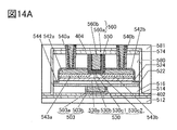
- 14A and 14B are schematic cross-sectional views each illustrating a structural example of a transistor.
- FIG. 15 is a schematic sectional view illustrating a configuration example of a semiconductor device.
- 16A and 16B are schematic cross-sectional views each illustrating a structural example of a transistor.
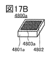
- 17A and 17B are perspective views showing an example of a semiconductor wafer.
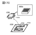
- FIG. 17C and 17D are perspective views showing an example of an electronic component.
- FIG. 18 is a perspective view and a schematic diagram illustrating an example of a product.
- FIG. 19 is a circuit diagram showing the configuration of the semiconductor device according to the example.
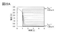
- 20A and 20B are graphs showing simulation results of the example.
- FIG. 21 is a circuit diagram showing the configuration of the semiconductor device according to the example.
- 22A to 22C are graphs showing simulation results of the example.
- the position, size, range, etc. of each configuration shown in the drawings and the like may not represent the actual position, size, range, etc. in order to facilitate understanding of the invention. Therefore, the disclosed invention is not necessarily limited to the position, size, range, or the like disclosed in the drawings and the like.
- a resist mask or the like may be unintentionally reduced due to a process such as etching, but it may not be reflected in the drawings for easy understanding.
- a top view also referred to as a “plan view”
- a perspective view and the like, some of the constituent elements may be omitted for easy understanding of the drawing.
- electrode and “wiring” do not functionally limit these components.
- electrode may be used as part of “wiring” and vice versa.
- electrode and wiring include the case where a plurality of “electrodes” and “wirings” are integrally formed.
- the resistance value of “resistance” may be determined depending on the length of wiring.
- the resistance value may be determined by connecting to a conductive layer having a resistivity different from that of the conductive layer used for the wiring.
- the resistance value may be determined by doping the semiconductor layer with an impurity.
- a “terminal” in an electric circuit refers to a portion where input or output of current or voltage and reception or transmission of a signal are performed. Therefore, part of the wiring or the electrode may function as a terminal.
- electrode B on insulating layer A it is not necessary that the electrode B is directly formed on the insulating layer A, and another structure is provided between the insulating layer A and the electrode B. Do not exclude those that contain elements.
- the functions of the source and the drain are switched with each other depending on operating conditions such as the case where a transistor having different polarities is adopted, the direction of current changes in circuit operation, and the like, which limits which is a source or a drain. Is difficult. Therefore, in this specification and the like, the terms source and drain can be used interchangeably.
- “electrically connected” includes a case of being directly connected and a case of being connected through “thing having some electric action”.
- the “object having some kind of electrical action” is not particularly limited as long as it can transfer an electric signal between the connection targets. Therefore, even in the case of being expressed as “electrically connected”, there is a case where the actual circuit does not have a physical connection portion and only the wiring extends. Further, even when it is expressed as “direct connection”, it includes a case where different conductive layers are connected via a contact. Note that there are cases where the wiring has different conductive layers containing one or more same elements and cases where the wiring contains different elements.
- the voltage often indicates a potential difference between a certain potential and a reference potential (for example, a ground potential or a source potential). Therefore, the voltage and the potential can be paraphrased in many cases. In this specification and the like, voltage and potential can be paraphrased unless otherwise specified.
- semiconductor even when described as “semiconductor”, for example, when the conductivity is sufficiently high, it has characteristics as “conductor”. Therefore, it is possible to replace the “semiconductor” with the “conductor” and use it. In this case, the boundary between the “semiconductor” and the “conductor” is ambiguous, and it is difficult to strictly distinguish the two. Therefore, the “semiconductor” and the “conductor” described in this specification and the like may be interchangeable in some cases.
- ordinal numbers such as “first” and “second” in this specification and the like are given to avoid confusion among components and do not indicate any order or order such as a process order or a stacking order. .. Further, even in the present specification, a term without an ordinal number may have an ordinal number in the claims in order to avoid confusion among components. Further, even if a term is given an ordinal number in this specification, a different ordinal number may be attached in the claims. Further, even if a term has an ordinal number in this specification, the ordinal number may be omitted in the claims and the like.
- the “on state” of a transistor refers to a state where the source and drain of the transistor can be regarded as being electrically short-circuited (also referred to as “conduction state”). Further, the “off state” of a transistor refers to a state where the source and drain of the transistor can be considered to be electrically disconnected (also referred to as a “non-conduction state”).
- the “on-state current” may refer to a current flowing between the source and the drain when the transistor is on.
- the “off current” may mean a current flowing between the source and the drain when the transistor is off.
- a gate refers to part or all of a gate electrode and a gate wiring.
- a gate wiring refers to a wiring for electrically connecting a gate electrode of at least one transistor to another electrode or another wiring.
- a source refers to part or all of a source region, a source electrode, and a source wiring.
- the source region refers to a region of the semiconductor layer whose resistivity is equal to or lower than a certain value.
- the source electrode refers to a conductive layer in a portion connected to the source region.
- a source wiring refers to a wiring for electrically connecting a source electrode of at least one transistor to another electrode or another wiring.
- a drain refers to part or all of a drain region, a drain electrode, and a drain wiring.
- the drain region refers to a region of the semiconductor layer whose resistivity is equal to or lower than a certain value.
- the drain electrode refers to a conductive layer in a portion connected to the drain region.
- the drain wiring refers to a wiring for electrically connecting the drain electrode of at least one transistor to another electrode or another wiring.
- the metal oxide is a metal oxide in a broad sense. Metal oxides are classified into oxide insulators, oxide conductors (including transparent oxide conductors), oxide semiconductors (Oxide Semiconductor or simply OS), and the like. For example, when a metal oxide is used for a semiconductor layer of a transistor, the metal oxide may be referred to as an oxide semiconductor. That is, the term “OS transistor” can be rephrased as a transistor including a metal oxide or an oxide semiconductor.
- metal oxides containing nitrogen may be collectively referred to as metal oxides. Further, the metal oxide containing nitrogen may be referred to as a metal oxynitride.
- One embodiment of the present invention is a semiconductor device in which a holding transistor is provided between a control circuit and an output transistor.
- the control circuit can have a configuration including an operational amplifier.
- the semiconductor device of one embodiment of the present invention can be applied to a semiconductor device having a function of continuously outputting a constant potential, such as a DC-DC converter, for example, a linear regulator.
- the constant potential can be output from the source or the drain of the output transistor.
- a node where the other of the source and the drain of the holding transistor and the gate of the output transistor are electrically connected is a holding node.
- the holding transistor When the holding transistor is turned on, the potential corresponding to the potential output from the control circuit is written in the holding node. After that, when the holding transistor is turned off, the potential of the holding node is held. Therefore, even if the control circuit is turned off, the gate potential of the output transistor can be maintained at a constant value. Therefore, even if the control circuit is turned off, a constant potential can be continuously output from, for example, the source or drain of the output transistor.
- the self-consumption current which is a current consumed in the control circuit and the like can be reduced, so that the power consumption of the semiconductor device of one embodiment of the present invention can be reduced.
- the holding transistor is preferably a transistor with extremely low off-state current, such as an OS transistor. Accordingly, the potential can be held at the holding node for a long time. Therefore, the frequency of writing the potential to the holding node can be reduced, so that power consumption of the semiconductor device of one embodiment of the present invention can be reduced.
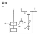
- FIG. 1A is a diagram illustrating a configuration example of a semiconductor device 10 which is a semiconductor device of one embodiment of the present invention.
- the semiconductor device 10 includes a control circuit 20, a power switch circuit 21, a transistor 22, and a transistor 23.
- the transistor 22 can be provided between the control circuit 20 and the transistor 23.
- the control circuit 20 can be configured to have, for example, a first power supply terminal, a second power supply terminal, a first input terminal, a second input terminal, and an output terminal.
- the first power supply terminal of the control circuit 20 can be electrically connected to the wiring 11.
- the second power supply terminal of the control circuit 20 can be electrically connected to the power supply switch circuit 21.
- the first input terminal of the control circuit 20 can be electrically connected to the wiring 15.
- the second input terminal of the control circuit 20 can be electrically connected to the wiring 16.
- the output terminal of the control circuit 20 can be electrically connected to one of the source and the drain of the transistor 22.
- a node NW where the output terminal of the control circuit 20 and one of the source and the drain of the transistor 22 are electrically connected.
- first power supply terminal and “second power supply terminal” can be replaced with each other as necessary or appropriate.
- the wiring 11 may be electrically connected to the second power supply terminal of the control circuit 20, and the power supply switch circuit 21 may be electrically connected to the first power supply terminal of the control circuit 20.
- first input terminal and the term “second input terminal” can be replaced with each other as necessary or appropriate.
- the wiring 15 may be electrically connected to the second input terminal of the control circuit 20, and the wiring 16 may be electrically connected to the first input terminal of the control circuit 20.
- the wiring 16 is electrically connected to the second input terminal of the control circuit 20 and one of a source and a drain of the transistor 23.
- the other of the source and the drain of the transistor 22 is electrically connected to the gate of the transistor 23. Further, the other of the source and the drain of the transistor 23 is electrically connected to the wiring 12.
- a node where the other of the source and the drain of the transistor 22 and the gate of the transistor 23 are electrically connected is a node NH.
- the wiring 11 and the wiring 12 have a function as a power supply line.
- the potentials of the wiring 11 and the wiring 12 can be, for example, high potential.
- a high potential refers to a potential higher than a low potential.
- the low potential is the ground potential
- the positive potential can be the high potential.
- the source potential is low and the potential of the transistor is on when it is applied to the gate of the n-channel transistor, it can be high and the off potential can be low.
- the potential can be high and the potential on can be low.
- the wiring 16 has a function as an output line that outputs a desired potential to the outside of the semiconductor device 10.
- the wiring 16 can be electrically connected to, for example, a device provided outside the semiconductor device 10.
- the control circuit 20 has a function of outputting a potential corresponding to the potential supplied to the input terminal from the output terminal.
- the wiring 16 electrically connected to the second input terminal has a function as an output line. Therefore, it can be said that the control circuit 20 is feedback-controlled. Accordingly, the control circuit 20 can output a potential corresponding to the potential of the wiring 15 electrically connected to the first input terminal.
- the potential of the wiring 15 can be referred to as a reference potential, for example.
- the power switch circuit 21 can control ON/OFF of the control circuit 20 by controlling a current or a potential supplied to the control circuit 20.
- the control circuit 20 being turned on means that the control circuit 20 can output a desired potential
- the control circuit 20 being turned off means that the control circuit 20 is turned off. Is not in a state capable of outputting a desired potential.
- the control circuit 20 when the control circuit 20 is on, the control circuit 20 outputs a potential corresponding to the potential of the wiring 15, and when the control circuit 20 is off, the control circuit 20 outputs the potential.
- the potential is a potential that does not correspond to the potential of the wiring 15.
- the transistor 22 has a function of controlling writing of a potential to the node NH. Specifically, the potential output from the control circuit 20 is written to the node NH when the transistor 22 is on, and the potential of the node NH is held when the transistor 22 is off. To be done. That is, it can be said that the transistor 22 is a holding transistor.
- the transistor 22 it is preferable to use a transistor having extremely low off-state current. Accordingly, the period in which the potential can be held at the node NH can be extremely extended.
- An OS transistor can be given as a transistor having extremely low off-state current. Specifically, the off-state current per 1 ⁇ m of the channel width can be less than 1 ⁇ 10 ⁇ 20 A, preferably less than 1 ⁇ 10 ⁇ 22 A, and more preferably less than 1 ⁇ 10 ⁇ 24 A at room temperature.
- the OS transistor has excellent electrical characteristics in a high temperature environment as compared with a transistor including silicon in a semiconductor layer (hereinafter also referred to as a Si transistor). Therefore, by using an OS transistor as a transistor included in the semiconductor device of one embodiment of the present invention, such as the transistor 22, a semiconductor device with stable operation even in a high temperature environment and favorable reliability can be realized.
- the transistor 23 has a function of outputting a potential corresponding to the potential of the node NH to the wiring 16. That is, the transistor 23 can be said to be an output transistor.
- the transistor 23 can be, for example, a p-channel transistor.
- the transistor 23 can be, for example, a Si transistor. Besides the transistor 23, a Si transistor can be used as a transistor included in the semiconductor device 10.
- the potential output from the control circuit 20 can be a potential corresponding to the potential of the wiring 15 and the potential output from the control circuit 20 is written and held in the node NH. Then, the potential of the wiring 16 becomes a potential corresponding to the potential of the node NH. From the above, the potential of the wiring 16 can be a potential corresponding to the potential of the wiring 15. For example, the potential of the wiring 16 can be the same as or substantially the same as the potential of the wiring 15.
- the semiconductor device 10 by turning on the control circuit 20 and turning on the transistor 22, the potential output from the control circuit 20 is written to the node NH. After that, the transistor 22 is turned off and the potential of the node NH is held, so that the semiconductor device 10 can continue to output a desired potential from the wiring 16 even when the control circuit 20 is turned off.
- the self-consumption current which is a current consumed inside the control circuit 20 and the like, can be reduced, so that the power consumption of the semiconductor device 10 can be reduced.
- the semiconductor device 10 can be applied to, for example, a semiconductor device having a function of continuously outputting a constant potential.
- the semiconductor device 10 can be applied to a DC-DC converter, a linear regulator, or the like.
- FIG. 1B is a modified example of the semiconductor device 10 having the configuration shown in FIG. 1A, and is different from the semiconductor device 10 having the configuration shown in FIG. 1A in that a capacitor 24 is provided.
- the capacitance value of the capacitive element 24 can be, for example, 100 aF or more and 100 pF or less, for example, 10 fF or more and 50 pF or less, and can be 100 fF or more and 10 pF or less, for example, 1 pF or more and 5 pF or less.
- One electrode of the capacitor 24 is electrically connected to the node NH.
- the other electrode of the capacitor 24 is electrically connected to the wiring 34.
- the wiring 34 has a function as a power supply line.
- the potential of the wiring 34 can be, for example, low potential, for example, ground potential.
- the amount of charge that can be held in the node NH can be increased. Therefore, the potential of the node NH can be held for a long time.
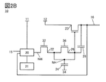
- FIG. 2A is a modified example of the semiconductor device 10 having the configuration shown in FIG. 1B, and is different from the semiconductor device 10 having the configuration shown in FIG. 1B in that it has a transistor 26.
- the transistor 22, the capacitor 24, and the transistor 26 can be provided between the control circuit 20 and the transistor 23.
- the source and the drain of the transistor 26 are electrically connected to the node NH.
- the gate of the transistor 26 is electrically connected to the wiring 36.
- the transistor 26 when the transistor 22 is turned on, the transistor 26 is turned off, and when the transistor 22 is turned off, the transistor 26 is turned on. Accordingly, when the transistor 22 is turned off, the potential of the node NH can be prevented from changing due to capacitive coupling of the capacitor 24 and the like. Therefore, the fluctuation of the potential of the wiring 16 can be suppressed, and the semiconductor device 10 can be stably operated.
- the semiconductor device 10 when the semiconductor device 10 is applied to a DC-DC converter, a linear regulator, or the like, it is preferable that the potential of the node NH does not fluctuate as much as possible because the output potential of the semiconductor device 10 requires high accuracy. Therefore, particularly when the semiconductor device 10 is applied to a DC-DC converter, a linear regulator, or the like, it is preferable to provide the transistor 26 in the semiconductor device 10.
- FIG. 2B is a modification of the semiconductor device 10 having the configuration shown in FIG. 2A, and is different from the semiconductor device 10 having the configuration shown in FIG. 2A in that the capacitor 28 is provided.
- the capacitance value of the capacitive element 28 can be, for example, greater than or equal to the capacitance value of the capacitive element 24.
- One electrode of the capacitor 28 is electrically connected to the node NH, and the other electrode of the capacitor 28 is electrically connected to the wiring 16.
- the potential of the wiring 16 decreases as the potential of the node NH increases, and the potential of the wiring 16 decreases as the potential of the node NH decreases. growing. Therefore, when the semiconductor device 10 is provided with the capacitance element 28, when the potential of one electrode of the capacitance element 28 increases, the potential of the other electrode of the capacitance element 28 increases and when the potential of one electrode of the capacitance element 28 decreases. The potential of the other electrode of the capacitor 28 becomes smaller. Therefore, the change in the potential of the wiring 16 due to the change in the potential of the node NH can be offset.
- the capacitor 28 can have a function similar to that of the capacitor 24. That is, it has a function of holding the potential of the node NH, for example. Therefore, when the semiconductor device 10 has the capacitive element 28, the semiconductor device 10 can be configured without the capacitive element 24. Alternatively, the capacitance value of the capacitive element 24 can be reduced.
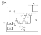
- FIG. 3A is a modified example of the semiconductor device 10 having the configuration shown in FIG. 2A, and is different from the semiconductor device 10 having the configuration shown in FIG. 2A in that the transistor 23 is not provided and the transistors 41 and 42 are provided. As illustrated in FIG. 3A, the transistor 22, the capacitor 24, and the transistor 26 can be provided between the control circuit 20 and the transistor 42.
- One of a source and a drain of the transistor 41 is electrically connected to the wiring 12.
- the other of the source and the drain of the transistor 41 and one of the source and the drain of the transistor 42 are electrically connected to the wiring 16.
- the other of the source and the drain of the transistor 42 is electrically connected to the wiring 52.
- the gate of the transistor 41 is electrically connected to the wiring 51.
- the gate of the transistor 42 is electrically connected to the node NH.
- a bias potential can be supplied to the wiring 51.
- the bias potential may be a constant potential, for example.
- the transistor 41 can function as a current source.
- the wiring 52 also has a function as a power supply line.
- the potential of the wiring 52 can be low potential, for example, ground potential.
- the transistors 41 and 42 can be, for example, n-channel transistors.
- the potential of the wiring 12 is high and the potential of the wiring 52 is low
- the transistors 41 and 42 are n-channel transistors
- the potential of the wiring 16 decreases and the potential of the node NH decreases as the potential of the node NH increases.
- the potential of the wiring 16 increases. That is, even if the p-channel type transistor is not used as the output transistor, the semiconductor device 10 can perform, for example, the same operation as when the p-channel type transistor is used as the output transistor.
- OS transistors can be used as the transistors 41 and 42.
- the OS transistor has superior electrical characteristics in a high temperature environment as compared with the Si transistor. Therefore, by using OS transistors as the transistors 41 and 42, the potential of the wiring 16 is stable even in a high temperature environment. Therefore, the potential output from the semiconductor device 10 is stable even in a high temperature environment, and the semiconductor device 10 can be operated stably.
- FIG. 3B is a modified example of the semiconductor device 10 having the configuration shown in FIG. 3A, and is different from the semiconductor device 10 having the configuration shown in FIG. 3A in that a capacitor 28 is provided. 2B, one electrode of the capacitor 28 is electrically connected to the node NH, and the other electrode of the capacitor 28 is electrically connected to the wiring 16.
- the semiconductor device 10 By configuring the semiconductor device 10 as shown in FIG. 3B, the semiconductor device 10 can be stably operated as in the case where the semiconductor device 10 is configured as shown in FIG. 2B.
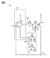
- FIG. 4 is a circuit diagram showing a specific configuration example of the semiconductor device 10 shown in FIG. 2A.
- FIG. 4 shows a circuit configuration example of the control circuit 20 and the power switch circuit 21.
- the control circuit 20 has an operational amplifier circuit 40.
- the power switch circuit 21 includes a transistor 44a, a transistor 44b, and a current source 45.
- the operational amplifier circuit 40 can be configured to have, for example, a first power supply terminal, a second power supply terminal, a first input terminal, a second input terminal, and an output terminal.
- the first and second power supply terminals, the first and second input terminals, and the output terminal of the operational amplifier circuit 40 are respectively connected to the first and second power supply terminals, the first and second input terminals of the control circuit 20, respectively. It can be a terminal or an output terminal.
- the first power supply terminal of the operational amplifier circuit 40 is electrically connected to the wiring 11.
- the second power supply terminal of the operational amplifier circuit 40 is electrically connected to one of the source and drain of the transistor 44a and one of the source and drain of the transistor 44b.
- a node to which the second power supply terminal of the operational amplifier circuit 40, one of the source and the drain of the transistor 44a, and one of the source and the drain of the transistor 44b are electrically connected is a node Nref.
- the first input terminal of the operational amplifier circuit 40 is electrically connected to the wiring 15.
- the second input terminal of the operational amplifier circuit 40 is electrically connected to the wiring 16.
- FIG. 4 shows a case where the non-inverting input terminal is the first input terminal of the operational amplifier circuit 40 and the inverting input terminal is the second input terminal of the operational amplifier circuit 40.
- the output terminal of the operational amplifier circuit 40 is electrically connected to the node NW.
- the other of the source and the drain of the transistor 44a is electrically connected to one electrode of the current source 45.
- the gate of the transistor 44a is electrically connected to the wiring 54a.
- the other electrode of the current source 45 is electrically connected to the wiring 55a.
- the other of the source and the drain of the transistor 44b is electrically connected to the wiring 55b.
- the gate of the transistor 44b is electrically connected to the wiring 54b.
- the wiring 55a and the wiring 55b function as a power supply line.
- the potentials of the wiring 55a and the wiring 55b can be low potential, for example, ground potential.
- the operational amplifier circuit 40 is turned on by turning on the transistor 44a and turning off the transistor 44b. Therefore, the operational amplifier circuit 40 can output a potential corresponding to the potential of the wiring 15, for example. On the other hand, when the transistor 44a is turned off and the transistor 44b is turned on, the operational amplifier circuit 40 is turned off. Therefore, the operational amplifier circuit 40 can stop the output of the potential, for example. Details of switching on/off of the operational amplifier circuit 40 will be described later.
- FIG. 5 is a modification of the semiconductor device 10 having the configuration shown in FIG. 4, and is different from the semiconductor device 10 having the configuration shown in FIG. 4 in that the transistor 23 is an n-channel transistor.
- the wiring 15 can be electrically connected to the inverting input terminal of the operational amplifier circuit 40, and the wiring 16 can be electrically connected to the non-inverting input terminal of the operational amplifier circuit 40.
- the transistor 23 When the transistor 23 is an n-channel transistor, the transistor 23 can be an OS transistor. As described above, the OS transistor has superior electrical characteristics in a high temperature environment as compared with the Si transistor. Therefore, by using an OS transistor as the transistor 23, the potential of the wiring 16 is stable even in a high temperature environment. Therefore, the potential output from the semiconductor device 10 is stable even in a high temperature environment, and the semiconductor device 10 can be operated stably.
- FIG. 6 is a circuit diagram showing a specific configuration example of the semiconductor device 10 shown in FIG. 4, and shows a circuit configuration example of the operational amplifier circuit 40.
- the operational amplifier circuit 40 includes a transistor 63a, a transistor 63b, a transistor 64a, a transistor 64b, a transistor 65a, and a transistor 65b.
- One of a source and a drain of the transistor 63a and one of a source and a drain of the transistor 63b are electrically connected to the wiring 11.
- the other of the source and the drain of the transistor 63a is electrically connected to one of the source and the drain of the transistor 64a.
- One of a source and a drain of the transistor 64a is electrically connected to one of a source and a drain of the transistor 22.
- the gate of the transistor 63a is electrically connected to the gate of the transistor 63b.
- the gate of the transistor 63b is electrically connected to the other of the source and the drain of the transistor 63b.
- the other of the source and the drain of the transistor 63b is electrically connected to one of the source and the drain of the transistor 64b.
- the other of the source and the drain of the transistor 64a and the other of the source and the drain of the transistor 64b are electrically connected to one of the source and the drain of the transistor 65a.
- the other of the source and the drain of the transistor 65a is electrically connected to the wiring 75a.
- the gate of the transistor 65a, the gate of the transistor 65b, and one of the source and the drain of the transistor 65b are electrically connected to the node Nref.
- the other of the source and the drain of the transistor 65b is electrically connected to the wiring 75b.
- the gate of the transistor 64a is electrically connected to the wiring 15 and the gate of the transistor 64b is electrically connected to the wiring 16. That is, the gate of the transistor 64a can be said to be the first input terminal of the operational amplifier circuit 40, and the gate of the transistor 64b can be said to be the second input terminal of the operational amplifier circuit 40.
- the wiring 75a and the wiring 75b function as a power supply line.
- the potential of the wiring 75a and the wiring 75b can be low potential, for example, ground potential.
- FIG. 7 is a modification of the semiconductor device 10 having the configuration shown in FIG. 6, and is different from the semiconductor device 10 having the configuration shown in FIG. As in the case shown in FIG. 2B, one electrode of the capacitor 28 is electrically connected to the node NH, and the other electrode of the capacitor 28 is electrically connected to the wiring 16.
- the semiconductor device 10 By configuring the semiconductor device 10 to have the capacitive element 28, the semiconductor device 10 can be stably operated as described above.
- FIG. 8 is a timing chart showing an example of an operating method of the semiconductor device 10 having the configuration shown in FIG. In FIG. 8, “H” indicates a high potential and “L” indicates a low potential. Note that in the following description, the potentials of the wiring 11 and the wiring 12 are high potentials. The potentials of the wiring 34, the wiring 55a, the wiring 55b, the wiring 75a, and the wiring 75b are low.
- the potential of the wiring 32 is low, the potential of the wiring 36 is high, the potential of the wiring 54a is low, and the potential of the wiring 54b is high.
- the transistor 22 is off, the transistor 26 is on, the transistor 44a is off, and the transistor 44b is on.
- the potential of the node Nref is low, so that no current flows through the transistor 65b and thus no current flows through the transistor 65a. Therefore, it can be said that the operational amplifier circuit 40 is off.
- the potential of the wiring 32 is low, the potential of the wiring 36 is high, the potential of the wiring 54a is high, and the potential of the wiring 54b is low.
- the transistor 22 is turned off, the transistor 26 is turned on, the transistor 44a is turned on, and the transistor 44b is turned off.
- the transistor 44a is turned on, a current flows from the current source 45 toward the node Nref, so that the potential of the node Nref rises.
- a current flows between the source and the drain of the transistor 65b.
- a current mirror is formed by the transistors 65a and 65b, current also flows through the transistor 65a. Therefore, a current flows between the wiring 11 and the wirings 75a and 75b, and the operational amplifier circuit 40 is turned on.
- the operational amplifier circuit 40 is turned off when the potential of the node Nref is low, and the operational amplifier circuit 40 is turned on when the potential of the node Nref is higher than the low potential.
- the potential of the wiring 32 is high, the potential of the wiring 36 is low, the potential of the wiring 54a is high, and the potential of the wiring 54b is low.
- the transistor 22 is turned on, the transistor 26 is turned off, the transistor 44a is turned on, and the transistor 44b is turned off.
- the potential of the wiring 16 becomes a potential corresponding to the potential of the node NH which is the gate potential of the transistor 23.
- the potential of the node NH can be a potential corresponding to the potential of the wiring 15.
- the potential of the wiring 16 becomes a potential corresponding to the potential of the wiring 15. Note that in FIG. 8, the potential of the node NH from time T2 to time T3 is equal to the potential of the node NW which is a node to which the output terminal of the control circuit 20 is electrically connected.
- the potential of the wiring 32 is low, the potential of the wiring 36 is high, the potential of the wiring 54a is high, and the potential of the wiring 54b is low.
- the transistor 22 is turned off, the transistor 26 is turned on, the transistor 44a is turned on, and the transistor 44b is turned off. With the transistor 22 turned off and the transistor 26 turned on, the potential of the node NH is held.
- the potential of the wiring 32 is low, the potential of the wiring 36 is high, the potential of the wiring 54a is low, and the potential of the wiring 54b is high.
- the transistor 22 is turned off, the transistor 26 is turned on, the transistor 44a is turned off, and the transistor 44b is turned on. Since the transistor 44a is turned off and the transistor 44b is turned on, the potential of the node Nref becomes low and current does not flow between the source and the drain of the transistor 65b. Accordingly, current does not flow between the source and the drain of the transistor 65a, so that the potential of one of the source and the drain of the transistor 65a approaches a high potential which is the potential of the wiring 11.
- the potential of the wiring 75a is low and lower than the potential of the wiring 11, so that the potential of one of the source and the drain of the transistor 65a increases. As a result, the potential of the node NW rises. As described above, the operational amplifier circuit 40 is turned off.
- the transistor 22 since the transistor 22 is off, the potential of the node NH does not vary even if the potential of the node NW varies. Therefore, even from time T4 to time T5 when the operational amplifier circuit 40 is off, the potential of the wiring 16 does not change from the potential from time T2 to time T4 when the operational amplifier circuit 40 is on.
- the potential of the node NW rises and the potential of the node NH does not change. Therefore, when the transistor 22 is an n-channel transistor, the source of the transistor 22 is electrically connected to the node NH. It will be composed. Therefore, when the potential to be written to the node NH is increased from time T2 to time T3, the difference between the gate potential of the transistor 22 and the source potential of the transistor 22 is small (the difference is a negative value when the transistor 22 is turned off). In some cases, the absolute value of the difference is large). Thus, the off-state current of the transistor 22 is reduced, so that the potential of the node NH can be held for a long time.
- the difference between the gate potential of the transistor 22 and the source potential of the transistor 22 is negative. Therefore, when the gate potential of the transistor 22 is equal to the source potential of the transistor 22, for example, the off-state current of the transistor 22 is smaller than when the gate potential of the transistor 22 and the source potential of the transistor 22 are both ground potential, and the potential of the node NH Can be held for a long time.
- the operational amplifier circuit 40 can be turned off after the operational amplifier circuit 40 is turned on and the potential is written in the node NH again.
- the above is an example of the operation method of the semiconductor device 10.
- the potential of the wiring 36 is high while the potential of the wiring 32 is low, and the potential of the wiring 36 is high while the potential of the wiring 32 is high.
- the potential is low. That is, it can be said that signals complementary to each other are supplied to the wiring 32 and the wiring 36.
- the potential of the wiring 54b is high while the potential of the wiring 54a is low, and the potential of the wiring 54b is low while the potential of the wiring 54a is high. There is. That is, it can be said that signals complementary to each other are supplied to the wiring 54a and the wiring 54b. Note that there may be a period in which both the wiring 32 and the wiring 36 have a low potential or a period in which both the wiring 32 and the wiring 36 have a high potential.
- both the wiring 54a and the wiring 54b may have a low potential, or a period in which both the wiring 54a and the wiring 54b have a high potential.
- both the wiring 32 and the wiring 36 may have a high potential or a low potential during a period within 20% of time T1 to time T5.
- both the wiring 54a and the wiring 54b may have a high potential or a low potential in a period within 20% of the time T1 to the time T5.
- the semiconductor device 10 can continue to output a desired potential even when the operational amplifier circuit 40 is turned off. As described above, when the operational amplifier circuit 40 is turned off, no current flows in the transistors 65a and 65b. Therefore, the self-power consumption can be reduced by operating the semiconductor device 10 by the method shown in FIG. 8, so that the power consumption of the semiconductor device 10 can be reduced.
- the transistor 22 is preferably a transistor with extremely low off-state current, such as an OS transistor. Accordingly, the potential can be kept held at the node NH for a long time, so that the period from time T4 to time T5 can be extended. Therefore, the frequency of writing the potential to the node NH can be reduced. That is, it is possible to reduce the frequency of performing the operations shown from time T1 to time T4. As a result, the power consumption of the semiconductor device 10 can be reduced.
- the semiconductor device 10 can be applied to a DC-DC converter, a linear regulator, or the like. These require high precision in the output potential.
- the transistor 22 can be a transistor with extremely low off-state current such as an OS transistor.
- the semiconductor device 10 is operated by the method shown in FIG. 8, as described above, when the transistor 22 is turned off, the difference between the gate potential of the transistor 22 and the source potential of the transistor 22 is small (the difference is negative). The absolute value of the difference becomes large).
- the semiconductor device 10 can continue to output the potential with high accuracy, and the semiconductor device 10 can be stably operated.
- This embodiment can be implemented in appropriate combination with any of the structures described in the other embodiments and the like.
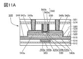
- the semiconductor device illustrated in FIG. 9 includes a transistor 300, a transistor 500, and a capacitor 600.
- 11A is a cross-sectional view of the transistor 500 in the channel length direction
- FIG. 11B is a cross-sectional view of the transistor 500 in the channel width direction
- FIG. 11C is a cross-sectional view of the transistor 300 in the channel width direction.
- the transistor 500 is an OS transistor.
- the off-state current of the transistor 500 is small. Therefore, for example, when the structure of the transistor 22 described in the above embodiment is similar to that of the transistor 500, the potential can be held at the node NH for a long time. Thus, the frequency of writing the potential to the node NH is reduced, so that power consumption of the semiconductor device can be reduced.
- the semiconductor device described in this embodiment includes a transistor 300, a transistor 500, and a capacitor 600 as illustrated in FIG.
- the transistor 500 is provided above the transistor 300
- the capacitor 600 is provided above the transistor 300 and the transistor 500.
- the transistor 23 described in the above embodiment can have a structure similar to that of the transistor 300
- the capacitor 24 can have a structure similar to that of the capacitor 600.
- the transistor 300 is provided over the substrate 311.
- the transistor 300 includes a conductor 316 and an insulator 315. Further, the transistor 300 includes a semiconductor region 313 formed of a part of the substrate 311, a low resistance region 314a which functions as a source region or a drain region, and a low resistance region 314b.
- the top surface of the semiconductor region 313 and the side surface in the channel width direction are covered with the conductor 316 with the insulator 315 interposed therebetween.
- the Fin type transistor 300 increases the effective channel width. Accordingly, the on characteristics of the transistor 300 can be improved. Further, since the electric field contribution of the gate electrode can be increased, the off characteristics of the transistor 300 can be improved.
- the transistor 300 may be either a p-channel type or an n-channel type.
- a region of the semiconductor region 313 in which a channel is formed, a region in the vicinity thereof, a low-resistance region 314a and a low-resistance region 314b which serve as a source region or a drain region, and the like preferably contain a semiconductor such as a silicon-based semiconductor, and a single crystal. It preferably contains silicon. Alternatively, a material including Ge (germanium), SiGe (silicon germanium), GaAs (gallium arsenide), GaAlAs (gallium aluminum arsenide), or the like may be used. A structure may be used in which silicon is used in which the effective mass is controlled by applying stress to the crystal lattice and changing the lattice spacing. Alternatively, the transistor 300 may be a HEMT (High Electron Mobility Transistor) by using GaAs and GaAlAs.
- HEMT High Electron Mobility Transistor
- the low-resistance region 314a and the low-resistance region 314b impart an n-type conductivity imparting element such as arsenic or phosphorus, or a p-type conductivity imparting boron, in addition to the semiconductor material applied to the semiconductor region 313. Including the element to do.
- the conductor 316 functioning as a gate electrode can be formed using a semiconductor material such as silicon containing an element imparting n-type conductivity such as arsenic or phosphorus, or an element imparting p-type conductivity such as boron. ..
- a conductive material such as a metal material, an alloy material, or a metal oxide material can be used.
- the threshold voltage of the transistor can be adjusted by selecting the material of the conductor. Specifically, it is preferable to use a material such as titanium nitride or tantalum nitride for the conductor. Further, in order to achieve both conductivity and embedding properties, it is preferable to stack and use a metal material such as tungsten or aluminum on the conductor, and it is particularly preferable to use tungsten in terms of heat resistance.
- the structure of the transistor 300 illustrated in FIG. 9 is an example, and the structure is not limited thereto, and an appropriate transistor may be used depending on a circuit structure or an operation method.
- the transistor 300 may have a structure similar to that of the transistor 500 which is an OS transistor as illustrated in FIG. Note that details of the transistor 500 will be described later.
- the transistor 300 illustrated in FIG. 10 can be applied to the n-channel transistor 23 illustrated in FIG. 5, for example.
- a unipolar circuit refers to a circuit in which all transistors are transistors of the same polarity, for example.
- a circuit in which all transistors are n-channel transistors can be said to be a unipolar circuit.
- An insulator 320, an insulator 322, an insulator 324, and an insulator 326 are sequentially stacked to cover the transistor 300.
- the insulator 320, the insulator 322, the insulator 324, and the insulator 326 for example, silicon oxide, silicon oxynitride, silicon nitride oxide, silicon nitride, aluminum oxide, aluminum oxynitride, aluminum nitride oxide, aluminum nitride, or the like is used. Good.
- silicon oxynitride refers to a material whose content of oxygen is higher than that of nitrogen
- silicon oxynitride is a material whose content of nitrogen is higher than that of oxygen.
- aluminum oxynitride refers to a material having a higher oxygen content than nitrogen as its composition
- aluminum oxynitride means a material having a higher nitrogen content than oxygen as its composition.
- the insulator 322 may have a function as a planarization film which planarizes a step formed by the transistor 300 or the like provided below the insulator 322.
- the upper surface of the insulator 322 may be flattened by a flattening treatment using a chemical mechanical polishing (CMP) method or the like in order to improve flatness.
- CMP chemical mechanical polishing
- the insulator 324 it is preferable to use a film having a barrier property such that hydrogen and impurities do not diffuse from the substrate 311, the transistor 300, or the like to a region where the transistor 500 is provided.
- a film having a barrier property against hydrogen for example, silicon nitride formed by a CVD method can be used.
- silicon nitride formed by a CVD method when hydrogen diffuses into a semiconductor element including an oxide semiconductor, such as the transistor 500, characteristics of the semiconductor element might be deteriorated in some cases. Therefore, it is preferable to use a film which suppresses diffusion of hydrogen between the transistor 500 and the transistor 300.
- the film that suppresses hydrogen diffusion is a film in which the amount of released hydrogen is small.
- the desorption amount of hydrogen can be analyzed using, for example, a thermal desorption gas analysis method (TDS).
- TDS thermal desorption gas analysis method
- the desorption amount of hydrogen in the insulator 324 is calculated by converting the desorption amount converted into hydrogen atoms into the area of the insulator 324 in the range of the surface temperature of the film from 50° C. to 500° C. Therefore, it may be 10 ⁇ 10 15 atoms/cm 2 or less, preferably 5 ⁇ 10 15 atoms/cm 2 or less.
- the insulator 326 preferably has a lower relative permittivity than the insulator 324.
- the dielectric constant of the insulator 326 is preferably less than 4, and more preferably less than 3.
- the relative dielectric constant of the insulator 326 is preferably 0.7 times or less, and more preferably 0.6 times or less that of the insulator 324.
- a conductor 328, a conductor 330, and the like which are connected to the capacitor 600 or the transistor 500 are embedded.
- the conductor 328 and the conductor 330 have a function as a plug or a wiring.
- the conductor having a function as a plug or a wiring may have a plurality of structures collectively given the same reference numeral. In this specification and the like, the wiring and the plug connected to the wiring may be integrated. That is, part of the conductor may function as a wiring, and part of the conductor may function as a plug.
- a conductive material such as a metal material, an alloy material, a metal nitride material, or a metal oxide material is used as a single layer or a laminated layer. be able to. It is preferable to use a high melting point material such as tungsten or molybdenum, which has both heat resistance and conductivity, and it is preferable to use tungsten. Alternatively, it is preferably formed of a low resistance conductive material such as aluminum or copper. Wiring resistance can be reduced by using a low-resistance conductive material.
- a wiring layer may be provided over the insulator 326 and the conductor 330.
- an insulator 350, an insulator 352, and an insulator 354 are sequentially stacked and provided.
- a conductor 356 is formed over the insulator 350, the insulator 352, and the insulator 354.
- the conductor 356 has a function of a plug connected to the transistor 300 or a wiring. Note that the conductor 356 can be provided using a material similar to that of the conductor 328 or the conductor 330.
- the insulator 350 like the insulator 324, an insulator having a barrier property against hydrogen is preferably used.
- the conductor 356 preferably contains a conductor having a barrier property against hydrogen.
- a conductor having a barrier property against hydrogen be formed in an opening provided in the insulator 350 having a barrier property against hydrogen.
- tantalum nitride or the like is preferably used as the conductor having a barrier property against hydrogen. Further, by stacking tantalum nitride and tungsten having high conductivity, diffusion of hydrogen from the transistor 300 can be suppressed while maintaining conductivity as a wiring. In this case, it is preferable that the tantalum nitride layer having a hydrogen barrier property is in contact with the insulator 350 having a hydrogen barrier property.
- a wiring layer may be provided over the insulator 354 and the conductor 356.
- an insulator 360, an insulator 362, and an insulator 364 are sequentially stacked and provided.
- a conductor 366 is formed over the insulator 360, the insulator 362, and the insulator 364.
- the conductor 366 has a function as a plug or a wiring. Note that the conductor 366 can be provided using a material similar to that of the conductor 328 or the conductor 330.
- the conductor 366 preferably contains a conductor having a barrier property against hydrogen.
- a conductor having a barrier property against hydrogen be formed in an opening portion provided in the insulator 360 having a barrier property against hydrogen.
- a wiring layer may be provided over the insulator 364 and the conductor 366.
- an insulator 370, an insulator 372, and an insulator 374 are sequentially stacked and provided.
- a conductor 376 is formed over the insulator 370, the insulator 372, and the insulator 374.
- the conductor 376 has a function as a plug or a wiring. Note that the conductor 376 can be provided using a material similar to that of the conductor 328 or the conductor 330.
- the conductor 376 preferably includes a conductor having a barrier property against hydrogen.
- a conductor having a barrier property against hydrogen be formed in an opening portion provided in the insulator 370 having a barrier property against hydrogen.
- a wiring layer may be provided over the insulator 374 and the conductor 376.
- an insulator 380, an insulator 382, and an insulator 384 are sequentially stacked and provided.
- a conductor 386 is formed over the insulator 380, the insulator 382, and the insulator 384.
- the conductor 386 has a function as a plug or a wiring. Note that the conductor 386 can be provided using a material similar to that of the conductor 328 or the conductor 330.
- the insulator 380 like the insulator 324, an insulator having a barrier property against hydrogen is preferably used.
- the conductor 386 preferably contains a conductor having a barrier property against hydrogen.
- a conductor having a barrier property against hydrogen be formed in an opening portion provided in the insulator 380 having a barrier property against hydrogen.
- the semiconductor device has been described above, the semiconductor device according to this embodiment It is not limited to this.
- the number of wiring layers similar to the wiring layer including the conductor 356 may be three or less, or the number of wiring layers similar to the wiring layer including the conductor 356 may be five or more.
- An insulator 510, an insulator 512, an insulator 514, and an insulator 516 are sequentially stacked over the insulator 384.
- Any of the insulator 510, the insulator 512, the insulator 514, and the insulator 516 is preferably formed using a substance having a barrier property against oxygen and hydrogen.
- the insulator 510 and the insulator 514 it is preferable to use a film having a barrier property such that hydrogen and impurities do not diffuse from the substrate 311 or the like, or from the region where the transistor 300 is provided to the region where the transistor 500 is provided. .. Therefore, it is preferable to use a material similar to that of the insulator 324.
- silicon nitride formed by a CVD method can be used as an example of a film having a barrier property against hydrogen.
- silicon nitride formed by a CVD method when hydrogen diffuses into a semiconductor element including an oxide semiconductor, such as the transistor 500, characteristics of the semiconductor element might be deteriorated in some cases. Therefore, it is preferable to use a film which suppresses diffusion of hydrogen between the transistor 500 and the transistor 300.
- the film that suppresses the diffusion of hydrogen is specifically a film in which the amount of released hydrogen is small.
- a metal oxide such as aluminum oxide, hafnium oxide, or tantalum oxide is preferably used for the insulator 510 and the insulator 514.
- aluminum oxide has a high blocking effect on both oxygen and impurities such as hydrogen and moisture which cause fluctuations in electrical characteristics of a transistor, which do not pass through the film. Therefore, aluminum oxide can prevent impurities such as hydrogen and moisture from entering the transistor 500 during and after the manufacturing process of the transistor. In addition, release of oxygen from the metal oxide included in the transistor 500 can be suppressed. Therefore, it is suitable to be used as a protective film for the transistor 500.
- the same material as that of the insulator 320 can be used for the insulator 512 and the insulator 516. Further, by applying a material having a relatively low dielectric constant to these insulators, it is possible to reduce the parasitic capacitance generated between the wirings.
- a silicon oxide film, a silicon oxynitride film, or the like can be used as the insulator 512 and the insulator 516.
- a conductor 518 In the insulator 510, the insulator 512, the insulator 514, and the insulator 516, a conductor 518, a conductor included in the transistor 500 (eg, the conductor 503), and the like are embedded. Note that the conductor 518 has a function of a plug connected to the capacitor 600 or the transistor 300, or a wiring.
- the conductor 518 can be provided using a material similar to that of the conductor 328 or the conductor 330.
- the conductor 518 in a region which is in contact with the insulator 510 and the insulator 514 is preferably a conductor having a barrier property against oxygen, hydrogen, and water.
- the transistor 300 and the transistor 500 can be separated by a layer having a barrier property against oxygen, hydrogen, and water, and diffusion of hydrogen from the transistor 300 to the transistor 500 can be suppressed.
- the transistor 500 is provided above the insulator 514.
- the transistor 500 includes a conductor 503 arranged so as to be embedded in an insulator 514 and an insulator 516 and an insulator 520 arranged over the insulator 516 and the conductor 503.
- An insulator 522 arranged on the insulator 520, an insulator 524 arranged on the insulator 522, an oxide 530a arranged on the insulator 524, and an oxide 530a arranged on the oxide 530a.
- the oxide 530b arranged, the conductor 542a and the conductor 542b arranged apart from each other on the oxide 530b, and the conductor 542a and the conductor 542b arranged between the conductor 542a and the conductor 542b.
- An insulator 580 in which an opening is overlapped and formed, an oxide 530c arranged so as to have a region in contact with a bottom surface and a side surface of the opening, an insulator 550 arranged in a formation surface of the oxide 530c, and an insulator. And a conductor 560 arranged on the formation surface of 550.
- the insulator 544 is preferably provided between the oxide 530a, the oxide 530b, the conductor 542a, and the insulator 580 and the insulator 580.
- the conductor 560 includes a conductor 560a provided inside the insulator 550 and a conductor 560b provided so as to be embedded inside the conductor 560a. It is preferable to have.
- an insulator 574 is preferably provided over the oxide 530c, the insulator 580, the conductor 560, and the insulator 550.
- the oxide 530a, the oxide 530b, and the oxide 530c may be collectively referred to as the oxide 530.
- the transistor 500 has a structure in which three layers of an oxide 530a, an oxide 530b, and an oxide 530c are stacked in a region where a channel is formed and in the vicinity thereof, the present invention is not limited to this. Not a thing. For example, a single layer of the oxide 530b, a two-layer structure of the oxide 530b and the oxide 530a, a two-layer structure of the oxide 530b and the oxide 530c, or a stacked structure of four or more layers may be provided. Further, in the transistor 500, the conductor 560 is illustrated as a stacked structure of two layers, but the present invention is not limited to this.
- the conductor 560 may have a single-layer structure or a stacked structure including three or more layers.
- the structure of the transistor 500 illustrated in FIGS. 9, 10, 11A, and 11B is an example, and the structure is not limited thereto, and an appropriate transistor may be used depending on a circuit structure or an operation method.
- the conductor 560 functions as a gate electrode of the transistor 500, and the conductors 542a and 542b function as a source electrode and a drain electrode, respectively.
- the conductor 560 is formed so as to be embedded in the opening of the insulator 580 and the region between the conductor 542a and the conductor 542b.
- the arrangement of the conductor 560, the conductor 542a, and the conductor 542b is selected in a self-aligned manner with respect to the opening of the insulator 580. That is, in the transistor 500, the gate electrode can be arranged in a self-aligned manner between the source electrode and the drain electrode. Therefore, the conductor 560 can be formed without providing a positioning margin, so that the area occupied by the transistor 500 can be reduced. As a result, the semiconductor device can be miniaturized and highly integrated.
- the conductor 560 is formed in a region between the conductor 542a and the conductor 542b in a self-aligned manner, the conductor 560 does not have a region overlapping with the conductor 542a or the conductor 542b. Accordingly, the parasitic capacitance formed between the conductor 560 and the conductors 542a and 542b can be reduced. Therefore, the switching speed of the transistor 500 is improved and high frequency characteristics can be obtained.
- the conductor 560 may function as a first gate (also referred to as a top gate) electrode.
- the conductor 503 may function as a second gate (also referred to as a bottom gate) electrode.
- the threshold voltage of the transistor 500 can be controlled by changing the potential applied to the conductor 503 independently of the potential applied to the conductor 560.
- the threshold voltage of the transistor 500 can be made higher than 0 V and the off-state current can be reduced. Therefore, applying a negative potential to the conductor 503 can reduce the drain current when the potential applied to the conductor 560 is 0 V, as compared to the case where no potential is applied.
- the conductor 503 is arranged so as to have a region overlapping with the oxide 530 and the conductor 560. Thus, when a potential is applied to the conductor 560 and the conductor 503, the electric field generated from the conductor 560 and the electric field generated from the conductor 503 are connected to cover a channel formation region formed in the oxide 530.
- a structure of a transistor in which a channel formation region is electrically surrounded by an electric field of a first gate electrode and a second gate electrode is referred to as a surrounded channel (s-channel) structure.
- the conductor 503 has a structure similar to that of the conductor 518, and the conductor 503a is formed in contact with the inner walls of the openings of the insulator 514 and the insulator 516, and the conductor 503b is formed further inside.
- the transistor 500 has a structure in which the conductor 503a and the conductor 503b are stacked, the present invention is not limited to this.
- the conductor 503 may have a single-layer structure or a stacked structure including three or more layers.
- the conductor 503a it is preferable to use a conductive material having a function of suppressing diffusion of impurities such as hydrogen atoms, hydrogen molecules, water molecules, and copper atoms (the above impurities are less likely to penetrate).
- a conductive material having a function of suppressing diffusion of oxygen eg, at least one of an oxygen atom and an oxygen molecule
- the function of suppressing diffusion of impurities or oxygen is a function of suppressing diffusion of any one or all of the above impurities and oxygen.
- the conductor 503a since the conductor 503a has a function of suppressing diffusion of oxygen, it is possible to prevent the conductor 503b from being oxidized and being reduced in conductivity.
- the conductor 503b is preferably formed using a conductive material having high conductivity, which contains tungsten, copper, or aluminum as its main component. In that case, the conductor 503a does not necessarily have to be provided.
- the conductor 503b is illustrated as a single layer, it may have a laminated structure, for example, a laminate of titanium or titanium nitride and the above conductive material.
- the insulator 520, the insulator 522, and the insulator 524 function as a second gate insulating film.
- the insulator 524 which is in contact with the oxide 530, an insulator containing more oxygen than oxygen which satisfies the stoichiometric composition is preferably used. That is, it is preferable that the insulator 524 be formed with an excess oxygen region. By providing such an insulator containing excess oxygen in contact with the oxide 530, oxygen vacancies in the oxide 530 can be reduced and the reliability of the transistor 500 can be improved.
- an oxide material in which part of oxygen is released by heating is preferably used.
- An oxide that desorbs oxygen by heating means that the amount of desorbed oxygen in terms of oxygen atoms is 1.0 ⁇ 10 18 atoms/cm 3 or more, preferably 1 or more by TDS (Thermal Desorption Spectroscopy) analysis.
- the surface temperature of the film during the TDS analysis is preferably 100° C. or higher and 700° C. or lower, or 100° C. or higher and 400° C. or lower.
- any one or more of heat treatment, microwave treatment, and RF treatment may be performed by contacting the insulator having the excess oxygen region with the oxide 530.
- water or hydrogen in the oxide 530 can be removed.
- reactions occur which bonds VoH is disconnected, when other words by reacting as "V O H ⁇ V O + H" occurs, it is possible to dehydrogenation.
- Part of the hydrogen generated at this time may be combined with oxygen and converted into H 2 O, which is removed from the oxide 530 or the insulator in the vicinity of the oxide 530.
- part of hydrogen may be diffused or captured (also referred to as gettering) in the conductor 542.
- a device having a power source for generating high-density plasma or a device having a power source for applying RF to the substrate side for the microwave treatment.
- a high-density oxygen radical can be generated by using a gas containing oxygen and using high-density plasma.
- oxygen radicals generated by high-density plasma can be efficiently introduced into the oxide 530 or the insulator near the oxide 530.
- the pressure may be 133 Pa or higher, preferably 200 Pa or higher, more preferably 400 Pa or higher.
- oxygen and argon are used, and an oxygen flow rate ratio (O 2 /(O 2 +Ar)) is 50% or less, preferably 10% or more and 30% or less. Good to do.
- heat treatment is preferably performed with the surface of the oxide 530 exposed.
- the heat treatment may be performed at 100 °C to 450 °C inclusive, more preferably 350 °C to 400 °C inclusive, for example.
- the heat treatment is performed in an atmosphere of a nitrogen gas or an inert gas, or an atmosphere containing an oxidizing gas at 10 ppm or more, 1% or more, or 10% or more.
- the heat treatment is preferably performed in an oxygen atmosphere. Accordingly, oxygen can be supplied to the oxide 530 to reduce oxygen vacancies (V 2 O 3 ).
- the heat treatment may be performed under reduced pressure.
- the heat treatment may be performed in an atmosphere containing an oxidizing gas in an amount of 10 ppm or higher, 1% or higher, or 10% or higher in order to supplement desorbed oxygen after the heat treatment is performed in a nitrogen gas or inert gas atmosphere.
- the heat treatment may be performed in an atmosphere containing an oxidizing gas in an amount of 10 ppm or more, 1% or more, or 10% or more, and then continuously performed in a nitrogen gas or inert gas atmosphere.
- the insulator 522 preferably has a function of suppressing diffusion of oxygen (eg, oxygen atoms, oxygen molecules, and the like) (oxygen is difficult to permeate).
- oxygen eg, oxygen atoms, oxygen molecules, and the like
- the insulator 522 have a function of suppressing diffusion of oxygen and impurities because oxygen included in the oxide 530 does not diffuse to the insulator 520 side. Further, the conductor 503 can suppress reaction with oxygen contained in the insulator 524 and the oxide 530, which is preferable.
- the insulator 522 is, for example, aluminum oxide, hafnium oxide, an oxide containing aluminum and hafnium (hafnium aluminate), tantalum oxide, zirconium oxide, lead zirconate titanate (PZT), strontium titanate (SrTiO 3 ), or It is preferable to use an insulator containing a so-called high-k material such as (Ba, Sr)TiO 3 (BST) in a single layer or a laminated layer. As transistors are miniaturized and highly integrated, thinning of the gate insulating film may cause problems such as leakage current. By using a high-k material for the insulator functioning as a gate insulating film, it is possible to reduce the gate potential during transistor operation while maintaining the physical film thickness.
- a so-called high-k material such as (Ba, Sr)TiO 3 (BST)
- an insulator containing an oxide of one or both of aluminum and hafnium which is an insulating material having a function of suppressing diffusion of impurities, oxygen, and the like (oxygen is difficult to permeate) is preferably used.
- the insulator containing one or both oxides of aluminum and hafnium aluminum oxide, hafnium oxide, an oxide containing aluminum and hafnium (hafnium aluminate), or the like is preferably used.
- the insulator 522 is formed using such a material, the insulator 522 suppresses release of oxygen from the oxide 530 and mixture of impurities such as hydrogen from the peripheral portion of the transistor 500 into the oxide 530. Functions as a layer.
- aluminum oxide, bismuth oxide, germanium oxide, niobium oxide, silicon oxide, titanium oxide, tungsten oxide, yttrium oxide, or zirconium oxide may be added to these insulators.
- these insulators may be nitrided. Silicon oxide, silicon oxynitride, or silicon nitride may be stacked over the above insulator and used.
- the insulator 520 is preferably thermally stable.
- silicon oxide and silicon oxynitride are preferable because they are thermally stable.
- an insulator of a high-k material by combining an insulator of a high-k material with silicon oxide or silicon oxynitride, an insulator 520 having a stacked structure which is thermally stable and has a high relative dielectric constant can be obtained.
- the insulator 520, the insulator 522, and the insulator 524 are illustrated as the second gate insulating film having a stacked-layer structure of three layers.
- the insulating film may have a single layer, two layers, or a laminated structure of four or more layers.
- the laminated structure is not limited to the same material, and may be a laminated structure made of different materials.
- the oxide 530 including the channel formation region is preferably formed using a metal oxide which functions as an oxide semiconductor.
- a metal oxide which functions as an oxide semiconductor.
- an In-M-Zn oxide the element M is aluminum, gallium, yttrium, copper, vanadium, beryllium, boron, titanium, iron, nickel, germanium, zirconium, molybdenum, lanthanum, cerium, neodymium.
- hafnium, tantalum, tungsten, magnesium, and the like One or more selected from hafnium, tantalum, tungsten, magnesium, and the like).
- the In-M-Zn oxide that can be applied as the oxide 530 is preferably a CAAC-OS (C-Axls Aligned Crystal Oxide Semiconductor) or a CAC-OS (Clood-Aligned Composite Oxide Semiconductor).
- a CAAC-OS C-Axls Aligned Crystal Oxide Semiconductor
- CAC-OS Clood-Aligned Composite Oxide Semiconductor
- an In—Ga oxide or an In—Zn oxide may be used as the oxide 530.
- the CAAC-OS and CAC-OS will be described later.
- a metal oxide having a low carrier concentration is preferably used.
- the concentration of impurities in the metal oxide may be lowered and the density of defect states may be lowered.
- low impurity concentration and low defect level density are referred to as high-purity intrinsic or substantially high-purity intrinsic.
- the impurities in the metal oxide include, for example, hydrogen, nitrogen, alkali metals, alkaline earth metals, iron, nickel, silicon and the like.
- hydrogen contained in a metal oxide reacts with oxygen bonded to a metal atom to be water, which may cause oxygen vacancies in the metal oxide.
- oxygen vacancies and hydrogen combine to form a V O H.
- V O H acts as a donor, sometimes electrons serving as carriers are generated.
- part of hydrogen may be bonded to oxygen which is bonded to a metal atom to generate an electron which is a carrier. Therefore, a transistor including a metal oxide containing a large amount of hydrogen is likely to have normally-on characteristics.
- the metal oxide easily moves due to stress such as heat and an electric field; therefore, when a large amount of hydrogen is contained in the metal oxide, reliability of the transistor might be deteriorated.
- the highly purified intrinsic or substantially highly purified intrinsic it is preferable that the highly purified intrinsic or substantially highly purified intrinsic.
- the impurities such as hydrogen (dehydration, may be described as dehydrogenation.)
- oxygenation treatment it is important to supply oxygen to the metal oxide to fill oxygen vacancies (sometimes referred to as oxygenation treatment).
- the metal oxide impurities is sufficiently reduced such V O H By using the channel formation region of the transistor, it is possible to have stable electrical characteristics.
- a defect in which hydrogen is contained in an oxygen vacancy can function as a metal oxide donor.
- the metal oxide may be evaluated not by the donor concentration but by the carrier concentration. Therefore, in this specification and the like, a carrier concentration which is assumed to be a state where an electric field is not applied is sometimes used as a parameter of a metal oxide, instead of a donor concentration. That is, the “carrier concentration” described in this specification and the like can be called the “donor concentration” in some cases.
- the hydrogen concentration obtained by secondary ion mass spectrometry is less than 1 ⁇ 10 20 atoms/cm 3 , preferably 1 ⁇ 10 19 atoms/cm 3. It is less than 3 , more preferably less than 5 ⁇ 10 18 atoms/cm 3 , and even more preferably less than 1 ⁇ 10 18 atoms/cm 3 .
- the carrier concentration of the metal oxide in the channel formation region is preferably 1 ⁇ 10 18 cm ⁇ 3 or lower, and less than 1 ⁇ 10 17 cm ⁇ 3. Is more preferable, less than 1 ⁇ 10 16 cm ⁇ 3 is more preferable, less than 1 ⁇ 10 13 cm ⁇ 3 is still more preferable, and less than 1 ⁇ 10 12 cm ⁇ 3 is further preferable.
- the lower limit of the carrier concentration of the metal oxide in the channel formation region is not particularly limited, but can be set to, for example, 1 ⁇ 10 ⁇ 9 cm ⁇ 3 .
- the conductor 542 (the conductor 542a and the conductor 542b) and the oxide 530 are in contact with each other, so that oxygen in the oxide 530 diffuses into the conductor 542,
- the conductor 542 may be oxidized. Oxidation of the conductor 542 is likely to reduce the conductivity of the conductor 542. Note that diffusion of oxygen in the oxide 530 to the conductor 542 can be restated as absorption of oxygen in the oxide 530 by the conductor 542.
- oxygen in the oxide 530 diffuses into the conductor 542 (the conductor 542a and the conductor 542b), so that the conductor 542a and the oxide 530b are separated from each other and the conductor 542b and the oxide 530b are separated from each other.
- a different layer is formed. Since the different layer contains more oxygen than the conductor 542, it is estimated that the different layer has an insulating property.
- the three-layer structure of the conductor 542, the different layer, and the oxide 530b can be regarded as a three-layer structure including a metal-insulator-semiconductor, which is called a MIS (Metal-Insulator-Semiconductor) structure. , Or a diode junction structure mainly composed of a MIS structure.
- the different layer is not limited to being formed between the conductor 542 and the oxide 530b.
- a different layer may be formed between the conductor 542 and the oxide 530c.
- it may be formed between the conductor 542 and the oxide 530b and between the conductor 542 and the oxide 530c.
- a metal oxide having a bandgap of 2 eV or more, preferably 2.5 eV or more is preferably used.
- the oxide 530 includes the oxide 530a below the oxide 530b, and thus can suppress diffusion of impurities into the oxide 530b from a structure formed below the oxide 530a. In addition, by having the oxide 530c over the oxide 530b, impurities can be prevented from diffusing into the oxide 530b from a structure formed above the oxide 530c.
- the oxide 530 preferably has a stacked structure including oxides in which the atomic ratio of each metal atom is different. Specifically, in the metal oxide used for the oxide 530a, the atomic ratio of the element M in the constituent elements is higher than the atomic ratio of the element M in the constituent elements in the metal oxide used for the oxide 530b. Is preferred. In the metal oxide used for the oxide 530a, the atomic ratio of the element M to In is preferably higher than the atomic ratio of the element M to In in the metal oxide used for the oxide 530b. In the metal oxide used for the oxide 530b, the atomic ratio of In to the element M is preferably higher than the atomic ratio of In to the element M in the metal oxide used for the oxide 530a. As the oxide 530c, a metal oxide that can be used for the oxide 530a or the oxide 530b can be used.
- the metal oxide having the composition of may be used.
- the energy of the bottom of the conduction band of the oxide 530a and the oxide 530c be higher than the energy of the bottom of the conduction band of the oxide 530b.
- the electron affinity of the oxide 530a and the oxide 530c be smaller than the electron affinity of the oxide 530b.
- the energy level at the bottom of the conduction band changes gently at the junction of the oxide 530a, the oxide 530b, and the oxide 530c.
- the energy level at the bottom of the conduction band at the junction of the oxide 530a, the oxide 530b, and the oxide 530c is continuously changed or continuously joined.
- the density of defect states in the mixed layer formed at the interface between the oxide 530a and the oxide 530b and the interface between the oxide 530b and the oxide 530c is preferably low.
- the oxide 530a and the oxide 530b, and the oxide 530b and the oxide 530c have a common element other than oxygen (as a main component), so that a mixed layer with low density of defect states is formed. can do.
- the oxide 530b is an In—Ga—Zn oxide
- In—Ga—Zn oxide, Ga—Zn oxide, gallium oxide, or the like may be used as the oxide 530a and the oxide 530c.
- the main path of carriers is the oxide 530b.
- the oxide 530a and the oxide 530c have the above structure, the density of defect states in the interface between the oxide 530a and the oxide 530b and the interface between the oxide 530b and the oxide 530c can be reduced. .. Therefore, the influence of interface scattering on carrier conduction is reduced and the transistor 500 can have high on-state current.
- the semiconductor material that can be used for the oxide 530 is not limited to the above metal oxide.
- a semiconductor material having a band gap (a semiconductor material that is not a zero-gap semiconductor) may be used.
- a semiconductor of a simple element such as silicon, a compound semiconductor such as gallium arsenide, a layered substance functioning as a semiconductor (also referred to as an atomic layer substance, a two-dimensional material, or the like) is preferably used as a semiconductor material.
- the layered substance is a general term for a group of materials having a layered crystal structure.
- the layered crystal structure is a structure in which layers formed by a covalent bond or an ionic bond are stacked via a bond weaker than the covalent bond or the ionic bond, such as van der Waals force.
- the layered material has high electric conductivity in the unit layer, that is, high two-dimensional electric conductivity.
- Layered substances include graphene, silicene, chalcogenides and the like.
- a chalcogenide is a compound containing chalcogen.
- chalcogen is a general term for elements belonging to Group 16 and includes oxygen, sulfur, selenium, tellurium, polonium, and livermolium.
- Examples of chalcogenides include transition metal chalcogenides and group 13 chalcogenides.
- a transition metal chalcogenide which functions as a semiconductor is preferably used.
- Specific examples of the transition metal chalcogenide applicable as the oxide 530 include molybdenum sulfide (typically MoS 2 ), molybdenum selenide (typically MoSe 2 ), molybdenum tellurium (typically MoTe 2 ).
- Tungsten sulfide typically WS 2
- tungsten selenide typically WSe 2
- tungsten tellurium typically WTe 2
- hafnium sulfide typically HfS 2
- hafnium selenide typically HfS 2
- hafnium selenide representative HFSE 2
- the sulfide zirconium typically ZrS 2 is
- the selenide zirconium typically include ZrSe 2 or the like.
- a conductor 542a and a conductor 542b which function as a source electrode and a drain electrode are provided over the oxide 530b.
- Examples of the conductor 542a and the conductor 542b are aluminum, chromium, copper, silver, gold, platinum, tantalum, nickel, titanium, molybdenum, tungsten, hafnium, vanadium, niobium, manganese, magnesium, zirconium, beryllium, indium, and ruthenium. It is preferable to use a metal element selected from iridium, strontium, and lanthanum, an alloy containing the above metal element as a component, an alloy in which the above metal elements are combined, or the like.
- the conductor 542a and the conductor 542b are illustrated as a single-layer structure in FIG. 11, they may be a stacked structure of two or more layers.
- a tantalum nitride film and a tungsten film may be stacked.
- a titanium film and an aluminum film may be stacked.
- a two-layer structure in which an aluminum film is stacked over a tungsten film a two-layer structure in which a copper film is stacked over a copper-magnesium-aluminum alloy film, a two-layer structure in which a copper film is stacked over a titanium film, and a tungsten film is formed over the tungsten film.
- a two-layer structure in which copper films are laminated may be used.
- a titanium film or a titanium nitride film a three-layer structure in which an aluminum film or a copper film is stacked over the titanium film or the titanium nitride film, and a titanium film or a titanium nitride film is further formed thereover, a molybdenum film, or
- a molybdenum nitride film and an aluminum film or a copper film are stacked over the molybdenum film or the molybdenum nitride film, and a molybdenum film or a molybdenum nitride film is formed thereover.
- a transparent conductive material containing indium oxide, tin oxide, or zinc oxide may be used.
- a region 543a and a region 543b may be formed as low resistance regions in the interface of the oxide 530 with the conductor 542a (conductor 542b) and in the vicinity thereof.
- the region 543a functions as one of the source region and the drain region
- the region 543b functions as the other of the source region and the drain region.
- a channel formation region is formed in a region between the region 543a and the region 543b.
- the oxygen concentration in the region 543a (region 543b) may be reduced.
- a metal compound layer containing a metal contained in the conductor 542a (conductor 542b) and a component of the oxide 530 may be formed in the region 543a (region 543b). In such a case, the carrier concentration of the region 543a (region 543b) increases, and the region 543a (region 543b) becomes a low resistance region.
- the insulator 544 is provided so as to cover the conductors 542a and 542b and suppresses oxidation of the conductors 542a and 542b. At this time, the insulator 544 may be provided so as to cover a side surface of the oxide 530 and be in contact with the insulator 524.
- insulator 544 a metal oxide containing one kind or two or more kinds selected from hafnium, aluminum, gallium, yttrium, zirconium, tungsten, titanium, tantalum, nickel, germanium, neodymium, lanthanum, magnesium, and the like is used. be able to. Further, as the insulator 544, silicon nitride oxide, silicon nitride, or the like can be used.
- the insulator 544 it is preferable to use aluminum oxide, hafnium oxide, an oxide containing aluminum and hafnium (hafnium aluminate), which is an insulator containing one or both oxides of aluminum and hafnium. ..
- hafnium aluminate has higher heat resistance than the hafnium oxide film. Therefore, crystallization is less likely to occur in heat treatment in a later step, which is preferable.
- the insulator 544 is not an essential component when the conductors 542a and 542b are materials that have oxidation resistance or when the conductivity does not significantly decrease even when oxygen is absorbed. It may be designed as appropriate according to the desired transistor characteristics.
- impurities such as water and hydrogen contained in the insulator 580 can be suppressed from diffusing into the oxide 530b through the oxide 530c and the insulator 550.
- oxidation of the conductor 560 due to excess oxygen in the insulator 580 can be suppressed.
- the insulator 550 functions as a first gate insulating film.
- the insulator 550 is preferably arranged so as to be in contact with the inside (top surface and side surface) of the oxide 530c.
- the insulator 550 is preferably formed using an insulator that contains excess oxygen and releases oxygen by heating.
- silicon oxide containing excess oxygen, silicon oxynitride, silicon nitride oxide, silicon nitride, silicon oxide containing fluorine, silicon oxide containing carbon, carbon oxide containing silicon and nitrogen, and voids The silicon oxide which it has can be used.
- silicon oxide and silicon oxynitride are preferable because they are stable to heat.
- the insulator 550 By providing an insulator from which oxygen is released by heating as the insulator 550 in contact with the upper surface of the oxide 530c, oxygen is effectively supplied from the insulator 550 to the channel formation region of the oxide 530b through the oxide 530c. can do. Further, similarly to the insulator 524, it is preferable that the concentration of impurities such as water or hydrogen in the insulator 550 be reduced.
- the thickness of the insulator 550 is preferably 1 nm or more and 20 nm or less.
- a metal oxide may be provided between the insulator 550 and the conductor 560 in order to efficiently supply the excess oxygen included in the insulator 550 to the oxide 530.
- the metal oxide preferably has a function of suppressing oxygen diffusion from the insulator 550 to the conductor 560.
- the metal oxide having a function of suppressing diffusion of oxygen diffusion of excess oxygen from the insulator 550 to the conductor 560 is suppressed. That is, a decrease in the excess oxygen amount supplied to the oxide 530 can be suppressed.
- oxidation of the conductor 560 due to excess oxygen can be suppressed.
- a material that can be used for the insulator 544 may be used.
- the insulator 550 may have a stacked-layer structure like the second gate insulating film.
- the insulator functioning as a gate insulating film has a stacked structure of a high-k material and a thermally stable material, so that the gate potential at the time of transistor operation can be increased while maintaining the physical film thickness. It becomes possible to reduce. Further, it is possible to form a laminated structure that is thermally stable and has a high relative dielectric constant.
- the conductor 560 functioning as the first gate electrode has a two-layer structure in FIGS. 11A and 11B, it may have a single-layer structure or a stacked structure of three or more layers.
- the conductor 560a has a function of suppressing diffusion of impurities such as hydrogen atoms, hydrogen molecules, water molecules, nitrogen atoms, nitrogen molecules, nitric oxide molecules (N 2 O, NO, NO 2, etc.), and copper atoms. It is preferable to use materials. Alternatively, it is preferable to use a conductive material having a function of suppressing diffusion of oxygen (eg, at least one of oxygen atoms and oxygen molecules). Since the conductor 560a has a function of suppressing diffusion of oxygen, it is possible to prevent the conductor 560b from being oxidized by oxygen contained in the insulator 550 and thus lowering conductivity.
- impurities such as hydrogen atoms, hydrogen molecules, water molecules, nitrogen atoms, nitrogen molecules, nitric oxide molecules (N 2 O, NO, NO 2, etc.), and copper atoms. It is preferable to use materials. Alternatively, it is preferable to use a conductive material having a function of suppressing diffusion of oxygen (eg, at least one of oxygen
- the conductive material having a function of suppressing diffusion of oxygen for example, tantalum, tantalum nitride, ruthenium, ruthenium oxide, or the like is preferably used.
- an oxide semiconductor which can be used for the oxide 530 can be used as the conductor 560a. In that case, by forming a film of the conductor 560b by a sputtering method, the electric resistance value of the conductor 560a can be reduced to be a conductor. This can be called an OC (Oxide Conductor) electrode.
- the conductor 560b is preferably formed using a conductive material containing tungsten, copper, or aluminum as its main component. Since the conductor 560b also functions as a wiring, it is preferable to use a conductor having high conductivity. For example, a conductive material containing tungsten, copper, or aluminum as its main component can be used. Further, the conductor 560b may have a stacked structure, for example, a stacked structure of titanium or titanium nitride and the above conductive material.
- the insulator 580 is provided over the conductor 542a and the conductor 542b with the insulator 544 interposed therebetween.
- the insulator 580 preferably has an excess oxygen region.
- silicon oxide, silicon oxynitride, silicon nitride oxide, silicon nitride, fluorine-added silicon oxide, carbon-added silicon oxide, carbon-nitrogen-added silicon oxide, or void-containing oxide is used. It is preferable to have silicon, resin, or the like.
- silicon oxide and silicon oxynitride are preferable because they are thermally stable.
- silicon oxide and silicon oxide having vacancies are preferable because an excess oxygen region can be easily formed in a later step.
- the insulator 580 preferably has an excess oxygen region.
- oxygen in the insulator 580 is efficiently transferred to the oxide 530a and the oxide 530b through the oxide 530c. Can be supplied. Note that the concentration of impurities such as water or hydrogen in the insulator 580 is preferably reduced.
- the opening of the insulator 580 is formed so as to overlap with a region between the conductor 542a and the conductor 542b.
- the conductor 560 is formed so as to be embedded in the opening of the insulator 580 and the region between the conductors 542a and 542b.
- the conductor 560 can have a shape with a high aspect ratio.
- the conductor 560 is provided so as to be embedded in the opening of the insulator 580, even if the conductor 560 has a high aspect ratio, the conductor 560 is not collapsed during the process. Can be formed.
- the insulator 574 is preferably provided in contact with the top surface of the insulator 580, the top surface of the conductor 560, and the top surface of the insulator 550.
- the excess oxygen region can be provided in the insulator 550 and the insulator 580. Accordingly, oxygen can be supplied into the oxide 530 from the excess oxygen region.
- insulator 574 a metal oxide containing one kind or two or more kinds selected from hafnium, aluminum, gallium, yttrium, zirconium, tungsten, titanium, tantalum, nickel, germanium, magnesium, or the like is used. You can
- aluminum oxide has a high barrier property and can suppress diffusion of hydrogen and nitrogen even in a thin film of 0.5 nm to 3.0 nm. Therefore, aluminum oxide formed by a sputtering method can have a function as a barrier film against impurities such as hydrogen as well as an oxygen supply source.
- an insulator 581 which functions as an interlayer film is preferably provided over the insulator 574.
- the insulator 581 preferably has a reduced concentration of impurities such as water or hydrogen in the film.
- the conductor 540a and the conductor 540b are provided in the openings formed in the insulator 581, the insulator 574, the insulator 580, and the insulator 544.
- the conductor 540a and the conductor 540b are provided to face each other with the conductor 560 interposed therebetween.
- the conductor 540a and the conductor 540b have the same structure as the conductor 546 and the conductor 548 described later.
- An insulator 582 is provided over the insulator 581.
- the insulator 582 it is preferable to use a substance having a barrier property against oxygen and hydrogen. Therefore, a material similar to that of the insulator 514 can be used for the insulator 582.
- the insulator 582 is preferably formed using a metal oxide such as aluminum oxide, hafnium oxide, or tantalum oxide.
- aluminum oxide has a high blocking effect of not permeating the film with respect to both oxygen and impurities such as hydrogen and moisture which cause fluctuations in electrical characteristics of the transistor. Therefore, aluminum oxide can prevent impurities such as hydrogen and moisture from entering the transistor 500 during and after the manufacturing process of the transistor. Further, release of oxygen from the oxide included in the transistor 500 can be suppressed. Therefore, it is suitable to be used as a protective film for the transistor 500.
- an insulator 586 is provided over the insulator 582.
- a material similar to that of the insulator 320 can be used.
- a material having a relatively low dielectric constant to these insulators, it is possible to reduce the parasitic capacitance generated between the wirings.
- a silicon oxide film, a silicon oxynitride film, or the like can be used as the insulator 586.
- the insulator 520, the insulator 522, the insulator 524, the insulator 544, the insulator 580, the insulator 574, the insulator 581, the insulator 582, and the insulator 586 include the conductor 546, the conductor 548, and the like. Is embedded.
- the conductor 546 and the conductor 548 have a function of a plug connected to the capacitor 600, the transistor 500, or the transistor 300, or a wiring.
- the conductor 546 and the conductor 548 can be provided using a material similar to that of the conductor 328 or the conductor 330.
- an opening may be formed so as to surround the transistor 500, and an insulator having a high barrier property against hydrogen or water may be formed so as to cover the opening.
- the plurality of transistors 500 may be collectively wrapped with an insulator having a high barrier property against hydrogen or water.
- an opening is formed so as to surround the transistor 500, for example, an opening reaching the insulator 514 or the insulator 522 is formed and the above-described insulator having a high barrier property is provided so as to be in contact with the insulator 514 or the insulator 522.
- the transistor 500 can serve as part of a manufacturing process of the transistor 500, which is preferable.
- the insulator having a high barrier property against hydrogen or water a material similar to that of the insulator 522 may be used, for example.
- the capacitor 600 is provided above the transistor 500.
- the capacitor 600 includes a conductor 610, a conductor 620, and an insulator 630.
- the conductor 612 may be provided over the conductor 546 and the conductor 548.
- the conductor 612 has a function as a plug connected to the transistor 500 or a wiring.
- the conductor 610 has a function as an electrode of the capacitor 600. Note that the conductor 612 and the conductor 610 can be formed at the same time.
- a metal film containing an element selected from molybdenum, titanium, tantalum, tungsten, aluminum, copper, chromium, neodymium, and scandium, or a metal nitride film containing the above element as a component (Tantalum nitride film, titanium nitride film, molybdenum nitride film, tungsten nitride film) or the like can be used.
- indium tin oxide, indium oxide containing tungsten oxide, indium zinc oxide containing tungsten oxide, indium oxide containing titanium oxide, indium tin oxide containing titanium oxide, indium zinc oxide, or silicon oxide is added. It is also possible to apply a conductive material such as indium tin oxide.
- the conductor 612 and the conductor 610 have a single-layer structure; however, the structure is not limited thereto and a stacked structure of two or more layers may be used.
- a conductor having a barrier property and a conductor having high adhesion to the conductor having a high conductivity may be formed between the conductor having a barrier property and the conductor having high conductivity.
- the conductor 620 is provided so as to overlap with the conductor 610 with the insulator 630 interposed therebetween.
- the conductor 620 can be formed using a conductive material such as a metal material, an alloy material, or a metal oxide material. It is preferable to use a high-melting-point material such as tungsten or molybdenum that has both heat resistance and conductivity, and it is particularly preferable to use tungsten.
- a low resistance metal material such as Cu (copper) or Al (aluminum) may be used.
- An insulator 640 is provided over the conductor 620 and the insulator 630.
- the insulator 640 can be provided using a material similar to that of the insulator 320. Further, the insulator 640 may function as a flattening film that covers the uneven shape below the insulator 640.
- FIGS. 12A and 12B are modified examples of the transistor 500 shown in FIGS. 11A and 11B.
- 12A is a cross-sectional view of the transistor 500 in the channel length direction
- FIG. 12B is a cross-sectional view of the transistor 500 in the channel width direction.
- the transistor 500 illustrated in FIGS. 12A and 12B is different from the transistor 500 illustrated in FIGS. 11A and 11B in that it includes an insulator 402 and an insulator 404.
- the insulator 552 is provided in contact with the side surface of the conductor 540a and the insulator 552 is provided in contact with the side surface of the conductor 540b, which is a difference from the transistor 500 illustrated in FIGS. 11A and 11B.
- the transistor 500 is different from the transistor 500 in FIGS. 11A and 11B in that the insulator 520 is not provided. Note that the structure illustrated in FIGS. 12A and 12B can be applied to another transistor included in the semiconductor device of one embodiment of the present invention, such as the transistor 300.
- the insulator 402 is provided over the insulator 512. Further, the insulator 404 is provided over the insulator 574 and the insulator 402.
- the insulator 514, the insulator 516, the insulator 522, the insulator 524, the insulator 544, the insulator 580, and the insulator 574 are patterned, and the insulator 404 is It is structured to cover. That is, the insulator 404 includes the upper surface of the insulator 574, the side surface of the insulator 574, the side surface of the insulator 580, the side surface of the insulator 544, the side surface of the insulator 524, the side surface of the insulator 522, the side surface of the insulator 516, and the insulating surface. The side surface of the body 514 and the upper surface of the insulator 402 are in contact with each other. Accordingly, the oxide 530 and the like are isolated from the outside by the insulator 404 and the insulator 402.
- the insulator 402 and the insulator 404 have a high function of suppressing diffusion of hydrogen (for example, at least one of hydrogen atoms and hydrogen molecules) or water molecules.
- hydrogen for example, at least one of hydrogen atoms and hydrogen molecules
- water molecules for example, water molecules.
- silicon nitride or silicon nitride oxide which is a material having a high hydrogen barrier property, is preferably used. Accordingly, hydrogen or the like can be suppressed from diffusing into the oxide 530, so that deterioration in characteristics of the transistor 500 can be suppressed. Therefore, reliability of the semiconductor device of one embodiment of the present invention can be improved.
- the insulator 552 is provided in contact with the insulator 581, the insulator 404, the insulator 574, the insulator 580, and the insulator 544.
- the insulator 552 preferably has a function of suppressing diffusion of hydrogen or water molecules.
- an insulator such as silicon nitride, aluminum oxide, or silicon nitride oxide, which is a material having a high hydrogen barrier property.
- silicon nitride is a material having a high hydrogen barrier property, and thus is preferably used as the insulator 552.
- the reliability of the semiconductor device of one embodiment of the present invention can be improved.
- FIG. 13 is a cross-sectional view illustrating a structural example of a semiconductor device when the transistors 500 and 300 have the structures illustrated in FIGS. 12A and 12B.
- An insulator 552 is provided on a side surface of the conductor 546.
- FIGS. 14A and 14B are modified examples of the transistors illustrated in FIGS. 12A and 12B.
- 14A is a cross-sectional view of the transistor in the channel length direction
- FIG. 14B is a cross-sectional view of the transistor in the channel width direction.
- the transistors illustrated in FIGS. 14A and 14B are different from the transistors illustrated in FIGS. 12A and 12B in that the oxide 530c has a two-layer structure of the oxide 530c1 and the oxide 530c2.
- the oxide 530c1 is in contact with the top surface of the insulator 524, the side surface of the oxide 530a, the top surface and side surface of the oxide 530b, the side surfaces of the conductors 542a and 542b, the side surface of the insulator 544, and the side surface of the insulator 580.
- the oxide 530c2 is in contact with the insulator 550.
- an In—Zn oxide can be used.
- a material similar to the material that can be used for the oxide 530c when the oxide 530c has a one-layer structure can be used.
- the on-state current of the transistor can be higher than in the case where the oxide 530c has a one-layer structure. Therefore, the transistor can be, for example, a power MOS transistor. Note that the oxide 530c included in the transistor illustrated in FIGS. 11A and 11B can also have a two-layer structure of the oxide 530c1 and the oxide 530c2.
- the transistors illustrated in FIGS. 14A and 14B can be applied to the transistor 300, for example.
- the transistor 300 can be applied to the transistor 23 illustrated in FIG. 5 in the above embodiment.
- the on-state current of the transistor 300 having the structure illustrated in FIGS. 14A and 14B is high. Therefore, by providing the transistor 23 having a function as an output transistor with the structure illustrated in FIGS. 14A and 14B, the on-state current of the transistor 23 can be increased. Therefore, the accuracy of the potential output from the semiconductor device of one embodiment of the present invention can be improved.
- the structure illustrated in FIGS. 14A and 14B can be applied to a transistor other than the transistor 300 included in the semiconductor device of one embodiment of the present invention, such as the transistor 500.
- FIG. 15 is a cross-sectional view illustrating a structural example of a semiconductor device in the case where the transistor 500 has the structure illustrated in FIGS. 11A and 11B and the transistor 300 has the structure illustrated in FIGS. 14A and 14B. Note that as in FIG. 13, the insulator 552 is provided on the side surface of the conductor 546. As illustrated in FIG. 15, in the semiconductor device of one embodiment of the present invention, both the transistors 300 and 500 can be OS transistors and the transistors 300 and 500 can have different structures.
- 16A and 16B are modified examples of the transistors illustrated in FIGS. 14A and 14B.
- 16A is a cross-sectional view of the transistor in the channel length direction
- FIG. 16B is a cross-sectional view of the transistor in the channel width direction.
- the transistor illustrated in FIGS. 16A and 16B is different from the transistor illustrated in FIGS. 14A and 14B in that it does not include the oxide 530b. That is, in the transistor illustrated in FIGS. 16A and 16B, the oxide 530 includes the oxide 530a, the oxide 530c1, and the oxide 530c2.
- the oxide 530 has a stacked structure of the oxide 530a, the oxide 530c1, and the oxide 530c2, the following excellent effects are obtained.
- the oxide 530c1 and the oxide 530c2 are U-shaped (U-) so as to extend along the openings formed in the insulator 580, the insulator 544, the conductor 542a, the conductor 542b, and the oxide 530a. Shape). Note that the opening formed in the oxide 530a does not reach the upper surface of the insulator 524. Alternatively, the side surface of the conductor 542a and the side surface of the conductor 542b and the side surface of the oxide 530c1 may be in contact with each other. Further, the oxide 530c2 is in contact with the upper surface of the oxide 530c1, so that the insulator 550 can be prevented from coming into contact with the oxide 530c1.
- the contact area between the conductor 542a and the conductor 542b and the oxide 530c1 can be reduced.
- the junction leakage current also referred to as a junction leakage current
- the contact area with the oxide 530c1 can be arbitrarily adjusted.
- a semiconductor device having a transistor having the structure shown in FIG. 16 can be preferably used when used in outer space.
- the transistor having the structure illustrated in FIG. 16 can be used as a transistor included in a semiconductor device provided in an artificial satellite.
- cosmic radiation or electrons or protons emitted from the sun may enter the inside of the semiconductor device and affect the semiconductor characteristics. Since the transistor having the structure shown in FIG. 16 has a reduced junction leakage current, it can be said that the transistor has a high resistance to cosmic radiation and a high reliability.
- This embodiment can be implemented in appropriate combination with any of the structures described in the other embodiments and the like.
- the CAC-OS or the CAC-metal oxide has a conductive function in a part of the material, an insulating function in a part of the material, and a function as a semiconductor in the whole material.
- a conductive function is a function of flowing electrons (or holes) serving as carriers
- an insulating function is a function of electrons serving as carriers. It is a function that does not flow.
- the CAC-OS or the CAC-metal oxide has a conductive region and an insulating region.
- the conductive region has the above-mentioned conductive function
- the insulating region has the above-mentioned insulating function.
- the conductive region and the insulating region may be separated at the nanoparticle level.
- the conductive region and the insulating region may be unevenly distributed in the material.
- the conductive region may be observed as a cloudy connection at the periphery and connected in a cloud shape.
- the conductive region and the insulating region are each dispersed in the material in a size of 0.5 nm to 10 nm, preferably 0.5 nm to 3 nm. There is.
- CAC-OS or the CAC-metal oxide is composed of components having different band gaps.
- CAC-OS or CAC-metal oxide is composed of a component having a wide gap due to the insulating region and a component having a narrow gap due to the conductive region.
- the carrier when the carrier flows, the carrier mainly flows in the component having the narrow gap.
- the component having the narrow gap acts complementarily to the component having the wide gap, and the carrier also flows to the component having the wide gap in conjunction with the component having the narrow gap. Therefore, when the CAC-OS or CAC-metal oxide is used in the channel formation region of the transistor, a high current driving force, that is, a large on-current and a high field-effect mobility can be obtained in the on-state of the transistor.
- the CAC-OS or the CAC-metal oxide can also be referred to as a matrix composite material or a metal matrix composite material.
- Oxide semiconductors are classified into single crystal oxide semiconductors and other non-single crystal oxide semiconductors.
- the non-single-crystal oxide semiconductor include a CAAC-OS, a polycrystalline oxide semiconductor, an nc-OS (nanocrystal oxide semiconductor), a pseudo-amorphous oxide semiconductor (a-like OS: amorphous-like oxide semiconductor), and the like. There are amorphous oxide semiconductors and the like.
- the CAAC-OS has a crystal structure having c-axis orientation and a strain in which a plurality of nanocrystals are connected in the ab plane direction.
- the strain refers to a portion in which the orientation of the lattice arrangement is changed between a region where the lattice arrangement is uniform and another region where the lattice arrangement is uniform in the region where a plurality of nanocrystals are connected.
- the nanocrystal is basically a hexagon, but is not limited to a regular hexagon, and may be a non-regular hexagon.
- the strain may have a lattice arrangement such as a pentagon and a heptagon.
- a clear crystal grain boundary also referred to as a grain boundary
- the formation of crystal grain boundaries is suppressed by the distortion of the lattice arrangement. This is because the CAAC-OS can tolerate strain due to the fact that the arrangement of oxygen atoms is not dense in the ab plane direction, the bond distance between atoms changes due to substitution with a metal element, or the like. It is thought to be because.
- the CAAC-OS is a layered crystal in which a layer containing indium and oxygen (hereinafter, an In layer) and a layer containing elements M, zinc, and oxygen (hereinafter, a (M,Zn) layer) are stacked. It tends to have a structure (also called a layered structure).
- indium and the element M can be replaced with each other, and when the element M of the (M,Zn) layer is replaced with indium, it can be expressed as an (In,M,Zn) layer.
- the indium of the In layer is replaced with the element M, it can be expressed as an (In,M) layer.
- CAAC-OS is an oxide semiconductor with high crystallinity.
- the CAAC-OS a clear crystal grain boundary cannot be confirmed, so that it can be said that a decrease in electron mobility due to the crystal grain boundary does not easily occur.
- the crystallinity of an oxide semiconductor might be lowered due to entry of impurities, generation of defects, or the like; therefore, it can be said that the CAAC-OS is an oxide semiconductor with few impurities and defects (oxygen vacancy or the like). Therefore, the oxide semiconductor including the CAAC-OS has stable physical properties. Therefore, the oxide semiconductor including the CAAC-OS is highly heat resistant and highly reliable. Further, the CAAC-OS is stable even at a high temperature (so-called thermal budget) in the manufacturing process. Therefore, when the CAAC-OS is used for the OS transistor, the degree of freedom in the manufacturing process can be increased.
- the nc-OS has a periodic atomic arrangement in a minute region (for example, a region of 1 nm or more and 10 nm or less, particularly a region of 1 nm or more and 3 nm or less). Moreover, in the nc-OS, no regularity is found in the crystal orientation between different nanocrystals. Therefore, no orientation is seen in the entire film. Therefore, the nc-OS may be indistinguishable from the a-like OS or the amorphous oxide semiconductor depending on the analysis method.
- the a-like OS is an oxide semiconductor having a structure between the nc-OS and the amorphous oxide semiconductor.
- the a-like OS has a void or a low density region. That is, the crystallinity of the a-like OS is lower than that of the nc-OS and the CAAC-OS.
- Oxide semiconductors have various structures and have different characteristics.
- the oxide semiconductor of one embodiment of the present invention may include two or more of an amorphous oxide semiconductor, a polycrystalline oxide semiconductor, an a-like OS, an nc-OS, and a CAAC-OS.
- an oxide semiconductor having a low carrier concentration is preferably used for the transistor.
- the concentration of impurities in the oxide semiconductor may be lowered and the density of defect states may be lowered.
- low impurity concentration and low defect level density are referred to as high-purity intrinsic or substantially high-purity intrinsic.
- a highly purified intrinsic or substantially highly purified intrinsic oxide semiconductor has a low density of defect states and thus has a low density of trap states in some cases.
- the charge trapped in the trap level of the oxide semiconductor takes a long time to disappear and may behave like fixed charge. Therefore, a transistor in which a channel formation region is formed in an oxide semiconductor with a high trap level density might have unstable electrical characteristics.
- Impurities include hydrogen, nitrogen, alkali metals, alkaline earth metals, iron, nickel, silicon and the like.
- the concentration of silicon or carbon in the oxide semiconductor and the concentration of silicon or carbon in the vicinity of the interface with the oxide semiconductor (the concentration obtained by secondary ion mass spectrometry (SIMS) are 2) It is set to be not more than ⁇ 10 18 atoms/cm 3 , preferably not more than 2 ⁇ 10 17 atoms/cm 3 .
- the oxide semiconductor contains an alkali metal or an alkaline earth metal
- a defect level might be formed and a carrier might be generated. Therefore, a transistor including an oxide semiconductor containing an alkali metal or an alkaline earth metal is likely to have normally-on characteristics. Therefore, it is preferable to reduce the concentration of alkali metal or alkaline earth metal in the oxide semiconductor.
- the concentration of an alkali metal or an alkaline earth metal in the oxide semiconductor obtained by SIMS is 1 ⁇ 10 18 atoms/cm 3 or less, preferably 2 ⁇ 10 16 atoms/cm 3 or less.
- the nitrogen concentration in the oxide semiconductor is less than 5 ⁇ 10 19 atoms/cm 3 in SIMS, preferably 5 ⁇ 10 18. Atoms/cm 3 or less, more preferably 1 ⁇ 10 18 atoms/cm 3 or less, and further preferably 5 ⁇ 10 17 atoms/cm 3 or less.
- the oxide semiconductor reacts with oxygen which is bonded to a metal atom to be water, which might cause oxygen deficiency.
- oxygen When hydrogen enters the oxygen vacancies, electrons which are carriers may be generated. Further, part of hydrogen may be bonded to oxygen which is bonded to a metal atom to generate an electron which is a carrier. Therefore, a transistor including an oxide semiconductor containing hydrogen is likely to have normally-on characteristics. Therefore, it is preferable that hydrogen in the oxide semiconductor be reduced as much as possible.
- the hydrogen concentration obtained by SIMS is less than 1 ⁇ 10 20 atoms/cm 3 , preferably less than 1 ⁇ 10 19 atoms/cm 3 , and more preferably 5 ⁇ 10 18 atoms/cm 3. It is less than 3 , and more preferably less than 1 ⁇ 10 18 atoms/cm 3 .
- This embodiment can be implemented in appropriate combination with any of the structures described in the other embodiments and the like.
- This embodiment shows an example of a semiconductor wafer in which the semiconductor device or the like shown in the above embodiment is formed, and an electronic component in which the semiconductor device is incorporated.
- a semiconductor wafer 4800 illustrated in FIG. 17A includes a wafer 4801 and a plurality of circuit portions 4802 provided on the top surface of the wafer 4801. A portion without the circuit portion 4802 on the upper surface of the wafer 4801 is a spacing 4803, which is a dicing area.
- the semiconductor wafer 4800 can be manufactured by forming a plurality of circuit portions 4802 on the surface of the wafer 4801 by a previous step. After that, the surface of the wafer 4801 opposite to the surface on which the plurality of circuit portions 4802 are formed may be ground to reduce the thickness of the wafer 4801. By this step, the warp of the wafer 4801 can be reduced and the size of the component can be reduced.
- a dicing process is performed as the next process.
- the dicing is performed along the scribe line SCL1 and the scribe line SCL2 (which may be referred to as a dicing line or a cutting line) indicated by a chain line.
- the spacing 4803 is provided so that the plurality of scribe lines SCL1 are parallel to each other and the plurality of scribe lines SCL2 are parallel to each other in order to easily perform the dicing process. It is preferable to provide the SCL2 vertically.
- a chip 4800a as shown in FIG. 17B can be cut out from the semiconductor wafer 4800.
- the chip 4800a includes a wafer 4801a, a circuit portion 4802, and a spacing 4803a. Note that it is preferable that the spacing 4803a be as small as possible. In this case, the width of the spacing 4803 between the adjacent circuit portions 4802 may be approximately the same as the cut margin of the scribe line SCL1 or the cut margin of the scribe line SCL2.
- the shape of the element substrate of one embodiment of the present invention is not limited to the shape of the semiconductor wafer 4800 illustrated in FIG. 17A.
- it may be a semiconductor wafer having a rectangular shape.
- the shape of the element substrate can be changed as appropriate depending on a manufacturing process of the element and an apparatus for manufacturing the element.
- FIG. 17C shows a perspective view of the electronic component 4700 and the substrate (mounting substrate 4704) on which the electronic component 4700 is mounted.
- the electronic component 4700 illustrated in FIG. 17C includes the lead 4701 and the chip 4800a described above, and functions as an IC chip or the like.
- the electronic component 4700 includes, for example, a wire bonding step of electrically connecting the lead 4701 of the lead frame and the electrode on the chip 4800a with a metal thin wire (wire), a molding step of sealing with an epoxy resin, and a lead frame. It can be manufactured by performing a plating process on the lead 4701 and a printing process on the surface of the package. Further, in the wire bonding process, for example, ball bonding, wedge bonding or the like can be used. Further, in FIG. 17C, QFP (Quad Flat Package) is applied to the package of the electronic component 4700, but the form of the package is not limited to this.
- QFP Quad Flat Package
- the electronic component 4700 is mounted on the printed board 4702, for example.
- a plurality of such IC chips are combined and electrically connected to each other on the printed board 4702, whereby the mounting board 4704 is completed.
- FIG. 17D shows a perspective view of electronic component 4730.
- the electronic component 4730 is an example of SiP (System in Package) or MCM (Multi Chip Module).
- an interposer 4731 is provided on a package board 4732 (printed board), and a semiconductor device 4735 and a plurality of semiconductor devices 4710 are provided on the interposer 4731.
- a wide band memory (HBM: High Bandwidth Memory) or the like can be used in addition to the semiconductor device described in the above embodiment.
- an integrated circuit semiconductor device such as a CPU, a GPU, an FPGA, or a memory device can be used.
- the package substrate 4732 a ceramic substrate, a plastic substrate, a glass epoxy substrate, or the like can be used.
- the interposer 4731 a silicon interposer, a resin interposer, or the like can be used.
- the interposer 4731 has a plurality of wirings and has a function of electrically connecting a plurality of integrated circuits having different terminal pitches.
- the plurality of wirings are provided in a single layer or a multilayer.
- the interposer 4731 has a function of electrically connecting an integrated circuit provided over the interposer 4731 to an electrode provided over the package substrate 4732.
- an interposer may be called a "rewiring board” or an "intermediate board.”
- a through electrode may be provided in the interposer 4731, and the integrated circuit and the package substrate 4732 may be electrically connected using the through electrode.
- TSV Through Silicon Via
- the interposer 4731 It is preferable to use a silicon interposer as the interposer 4731. Since the silicon interposer does not require an active element, it can be manufactured at a lower cost than an integrated circuit. On the other hand, since the wiring of the silicon interposer can be formed by a semiconductor process, it is easy to form fine wiring, which is difficult with the resin interposer.
- the interposer on which the HBM is mounted is required to form fine and high-density wiring. Therefore, it is preferable to use the silicon interposer as the interposer for mounting the HBM.
- the reliability is unlikely to decrease due to the difference in expansion coefficient between the integrated circuit and the interposer.
- the silicon interposer has a high surface flatness, a defective connection between the integrated circuit provided on the silicon interposer and the silicon interposer is unlikely to occur.
- a 2.5D package 2.5-dimensional mounting
- a heat sink heat dissipation plate
- the heights of the integrated circuits provided on the interposer 4731 be uniform.
- the semiconductor device 4710 and the semiconductor device 4735 have the same height.
- An electrode 4733 may be provided on the bottom of the package substrate 4732 to mount the electronic component 4730 on another substrate.
- FIG. 17D shows an example in which the electrode 4733 is formed of a solder ball.
- BGA Ball Grid Array
- the electrode 4733 may be formed using a conductive pin.
- PGA Peripheral Component Interconnect
- the electronic component 4730 can be mounted on another substrate using various mounting methods other than BGA and PGA.
- SPGA Sttaggered Pin Grid Array
- LGA Land Grid Array
- QFP Quad Flat Package
- QFJ Quad Flat J-leaded package
- QFN Quad non-Flade
- This embodiment can be implemented in appropriate combination with any of the structures described in the other embodiments and the like.
- FIG. 18 illustrates a state where an electronic component 4700 including the semiconductor device is included in each electronic device.
- the information terminal 5500 illustrated in FIG. 18 is a mobile phone (smartphone) that is a type of information terminal.
- the information terminal 5500 includes a housing 5510 and a display portion 5511.
- a touch panel is provided in the display portion 5511 and a button is provided in the housing 5510 as an input interface.
- the information terminal 5500 with low power consumption can be realized.
- low power consumption can reduce heat generation from a circuit, so that the influence of heat generation on the circuit itself, peripheral circuits, and modules can be reduced. Thereby, the reliability of the information terminal 5500 can be improved.
- FIG. 18 illustrates a smart watch 5900 as an example of a wearable terminal.
- the smartwatch 5900 includes a housing 5901, a display portion 5902, operation buttons 5903, operators 5904, a band 5905, and the like.
- the wearable terminal can realize a low power consumption wearable terminal by applying the semiconductor device described in any of the above embodiments. Moreover, since heat generation from a circuit can be reduced by low power consumption, the influence of the heat generation on the circuit itself, peripheral circuits, and modules can be reduced. Thereby, the reliability of the wearable terminal can be improved.
- FIG. 18 shows a desktop information terminal 5300.
- the desktop information terminal 5300 has a main body 5301 of the information terminal, a display 5302, and a keyboard 5303.
- the desktop information terminal 5300 can realize the desktop information terminal 5300 with low power consumption by applying the semiconductor device described in the above embodiment. Moreover, since heat generation from a circuit can be reduced by low power consumption, the influence of the heat generation on the circuit itself, peripheral circuits, and modules can be reduced. Thereby, the reliability of the desktop information terminal 5300 can be improved.
- a smartphone, a smart watch, and a desktop information terminal are shown as examples of electronic devices in FIG. 18, but information terminals other than the smartphone, smart watch, and desktop information terminal can be applied. ..
- Examples of information terminals other than smartphones, smart watches, and desktop information terminals include PDA (Personal Digital Assistant), notebook information terminals, workstations, and the like.
- FIG. 18 illustrates an electric refrigerator-freezer 5800 as an example of an electric appliance.
- the electric refrigerator-freezer 5800 includes a housing 5801, a refrigerator compartment door 5802, a freezer compartment door 5803, and the like.
- the electric refrigerator-freezer 5800 By applying the semiconductor device described in the above embodiment to the electric refrigerator-freezer 5800, the electric refrigerator-freezer 5800 with low power consumption can be realized. Moreover, since heat generation from a circuit can be reduced by low power consumption, the influence of the heat generation on the circuit itself, peripheral circuits, and modules can be reduced. Thereby, the reliability of the electric refrigerator-freezer 5800 can be improved.
- an electric refrigerator-freezer is described as an electric appliance, but other electric appliances include, for example, a vacuum cleaner, a microwave oven, a microwave oven, a rice cooker, a water heater, an IH cooker, a water server, and an air conditioner including an air conditioner. Examples include appliances, washing machines, dryers and audiovisual equipment.
- FIG. 18 illustrates a portable game machine 5200 which is an example of a game machine.
- the portable game machine 5200 includes a housing 5201, a display portion 5202, buttons 5203, and the like.
- FIG. 18 illustrates a stationary game machine 7500 which is an example of a game machine.
- the stationary game machine 7500 has a main body 7520 and a controller 7522.
- a controller 7522 can be connected to the main body 7520 wirelessly or by wire.
- the controller 7522 may include a display unit for displaying a game image, a touch panel or a stick that serves as an input interface other than buttons, a rotary knob, a slide knob, and the like.
- the controller 7522 is not limited to the shape shown in FIG. 18, and the shape of the controller 7522 may be variously changed according to the genre of the game.
- a trigger can be used as a button and a controller simulating a gun can be used.
- a controller having a shape imitating a musical instrument, a musical instrument, or the like can be used.
- the stationary game machine may be provided with a camera, a depth sensor, a microphone, etc. instead of using the controller, and may be operated by the game player's gesture and/or voice.
- the image of the game machine described above can be displayed on a display device such as a television device, a display for personal computer, a display for game, a head mounted display or the like.
- a display device such as a television device, a display for personal computer, a display for game, a head mounted display or the like.
- the portable game machine 5200 with low power consumption or the stationary game machine 7500 can be realized. Moreover, since heat generation from a circuit can be reduced by low power consumption, the influence of the heat generation on the circuit itself, peripheral circuits, and modules can be reduced. Thereby, the reliability of the portable game machine 5200 or the stationary game machine 7500 can be improved.
- FIG. 18 illustrates a portable game machine and a stationary game machine as examples of the game machine
- the electronic device of one embodiment of the present invention is not limited to this.
- Examples of the electronic device of one embodiment of the present invention include an arcade game machine installed in an entertainment facility (game center, amusement park, etc.), a batting practice pitching machine installed in a sports facility, and the like.
- a digital camera 6240 is shown in FIG.
- the digital camera 6240 includes a housing 6241, a display portion 6242, operation buttons 6243, a shutter button 6244, and the like.
- a detachable lens 6246 is attached to the digital camera 6240.
- the digital camera 6240 has a configuration in which the lens 6246 can be removed from the housing 6241 and can be replaced, the lens 6246 and the housing 6241 may be integrated. Further, the digital camera 6240 may be configured such that a strobe device, a viewfinder, etc. can be separately mounted.
- the low power consumption digital camera 6240 can be realized. Moreover, since heat generation from a circuit can be reduced by low power consumption, the influence of the heat generation on the circuit itself, peripheral circuits, and modules can be reduced. Thereby, the reliability of the digital camera 6240 can be improved.
- Video camera The semiconductor device described in any of the above embodiments can be applied to a video camera.
- a video camera 6300 is shown in FIG.
- the video camera 6300 includes a first housing 6301, a second housing 6302, a display portion 6303, operation keys 6304, a lens 6305, a connecting portion 6306, and the like.
- the operation key 6304 and the lens 6305 are provided in the first housing 6301, and the display portion 6303 is provided in the second housing 6302.
- the first housing 6301 and the second housing 6302 are connected by the connecting portion 6306, and the angle between the first housing 6301 and the second housing 6302 can be changed by the connecting portion 6306. is there.
- the image on the display portion 6303 may be switched according to the angle between the first housing 6301 and the second housing 6302 in the connection portion 6306.
- the video camera 6300 with low power consumption can be realized. Moreover, since heat generation from a circuit can be reduced by low power consumption, the influence of the heat generation on the circuit itself, peripheral circuits, and modules can be reduced. Thereby, the reliability of the video camera 6300 can be improved.
- ICD implantable defibrillator
- FIG. 18 is a schematic sectional view showing an example of the ICD.
- the ICD main body 5400 includes at least a battery 5401, an electronic component 4700, an antenna 5404, a wire 5402 to the right atrium, and a wire 5403 to the right ventricle.
- the ICD main body 5400 is placed in the body by surgery, and two wires are passed through the subclavian vein 5405 and the superior vena cava 5406 of the human body and one wire tip is placed in the right ventricle and the other wire tip is placed in the right atrium. To be done.
- the ICD main body 5400 has a function as a pacemaker and performs pacing on the heart when the heart rate is out of the specified range. If heart rate does not improve due to pacing (fast ventricular tachycardia, ventricular fibrillation, etc.), treatment with electric shock is performed.
- the ICD body 5400 needs to constantly monitor heart rate for proper pacing and electric shock. Therefore, the ICD main body 5400 has a sensor for detecting the heart rate. Further, the ICD main body 5400 can store heart rate data acquired by the sensor or the like, the number of times pacing treatment is performed, time, and the like.
- the ICD main body 5400 has a plurality of batteries, safety can be improved. Specifically, even if a part of the battery of the ICD main body 5400 becomes unusable, the remaining battery can be made to function, so that it also functions as an auxiliary power source.
- an antenna capable of transmitting a physiological signal may be provided, and for example, a physiological signal such as a pulse rate, a respiratory rate, a heart rate, and body temperature can be confirmed by an external monitor device.
- a physiological signal such as a pulse rate, a respiratory rate, a heart rate, and body temperature can be confirmed by an external monitor device.
- a system for monitoring active heart activity may be configured.
- the ICD main body 5400 By applying the semiconductor device described in the above embodiment to the ICD main body 5400, the ICD main body 5400 with low power consumption can be realized. Moreover, since heat generation from a circuit can be reduced by low power consumption, the influence of the heat generation on the circuit itself, peripheral circuits, and modules can be reduced. Thereby, the reliability of the ICD main body 5400 can be improved.
- the artificial satellite 6800 has a body 6801, a solar panel 6802, and an antenna 6803.
- the semiconductor device applied to the artificial satellite 6800 can generate a signal, for example.
- the signal is transmitted via the antenna 6803 and can be received by, for example, a receiver provided on the ground or another satellite.
- a receiver provided on the ground or another satellite.
- the position of the receiver that has received the signal can be measured. From the above, the artificial satellite 6800 can form a satellite positioning system, for example.
- the semiconductor device applied to the artificial satellite 6800 can have a structure including a sensor, for example.
- the artificial satellite 6800 can have a function of detecting sunlight reflected by an object provided on the ground.
- the artificial satellite 6800 can have a function of detecting thermal infrared rays emitted from the ground surface by being configured to have a thermal infrared sensor. From the above, the artificial satellite 6800 can have a function as, for example, an earth observation satellite.
- the semiconductor device described in any of the above embodiments is a low power consumption semiconductor device. Therefore, by applying the semiconductor device described in any of the above embodiments to the artificial satellite 6800, power consumption of the artificial satellite 6800 can be reduced. As a result, it is not necessary to provide a large capacity battery for the artificial satellite 6800, and the weight of the artificial satellite 6800 can be reduced. Therefore, the cost of launching the artificial satellite 6800 from the ground can be reduced.
- a semiconductor device or the like provided in the artificial satellite 6800 may be exposed to a high temperature environment of 200° C. or higher in a region where sunlight is irradiated.
- the semiconductor device described in the above embodiment has high reliability even in a high temperature environment. Therefore, by applying the semiconductor device of one embodiment of the present invention to the artificial satellite 6800, the reliability of the artificial satellite 6800 can be increased.
- This embodiment can be implemented in appropriate combination with any of the structures described in the other embodiments and the like.
- FIG. 19 is a circuit diagram showing the configuration of the circuit assumed in this embodiment.
- a circuit including the semiconductor device 10 having the configuration shown in FIG. 6 and a load circuit 13 provided outside the semiconductor device 10 and electrically connected to the wiring 16 The operation was performed on the simulation by the method shown in FIG.
- the load circuit 13 is configured to include a transistor 46a, a transistor 46b, a capacitor 47, and a current source 48.
- One of the source and the drain of the transistor 46a and the one electrode of the capacitor 47 was electrically connected to the wiring 16.
- the other electrode of the capacitor 47 was electrically connected to the wiring 57.
- the other of the source and the drain of the transistor 46a was electrically connected to the wiring 56a.
- the gate of the transistor 46a was electrically connected to the gate of the transistor 46b.
- the gate of the transistor 46b was electrically connected to one of the source and the drain of the transistor 46b.
- One of a source and a drain of the transistor 46b was electrically connected to one electrode of the current source 48.
- the other electrode of the current source 48 was electrically connected to the wiring 58.
- the other of the source and the drain of the transistor 46b was electrically connected to the wiring 56b.
- the potential of the wiring 11 is 3.3 V
- the capacitance value of the capacitor element 24 is 1 pF
- the current value of the current source 45 is 0.1 ⁇ A
- the capacitance value of the capacitor element 47 is 1 ⁇ F
- the current value of the current source 48 is 1 ⁇ A. ..
- the potentials of the wiring 34, the wiring 55a, the wiring 55b, the wiring 56a, the wiring 56b, the wiring 57, the wiring 58, the wiring 75a, and the wiring 75b are set to the ground potential. Assuming the above conditions, the operation of the semiconductor device 10 when 1.2 V is supplied to the wiring 15 as a reference potential was verified by simulation.
- FIG. 20A is a graph showing changes over time in the potentials of the wiring 32 and the wiring 54a.
- FIG. 20B is a graph showing changes over time in the potentials of the wiring 16, the node NW, the node NH, and the node Nref.
- the operation corresponding to the time T1 to the time T2 is performed for 0.0s to 0.5s
- the operation corresponding to the time T2 to the time T3 is performed for 0.5s to 1.5s
- the operation for 1.5s is performed.
- the operation corresponding to the time T3 to the time T4 was performed in the period from 2.0 s to 2.0 s
- the operation corresponding to the time T4 to the time T5 was performed in the simulation in the period 2.0 s to 4.0 s.
- the operation corresponding to the time T1 to the time T2 is performed during 4.0 s to 4.5 s
- the operation corresponding to the time T2 to the time T3 is performed between 4.5 s to 5.5 s
- An operation corresponding to time T3 to time T4 was performed during 6.0 s
- an operation corresponding to time T4 to time T5 was performed during simulation between 6.0 s and 8.0 s.
- the potential of the wiring 16 is approximately the same as the potential of the wiring 15, which is 1.2 V, and it was confirmed by simulation that the semiconductor device 10 can continue to output a desired potential.
- FIG. 21 shows a configuration in which the load circuit 13 having the configuration shown in FIG. 19 is provided outside the semiconductor device 10 having the configuration shown in FIG. 7, and the load circuit 13 is electrically connected to the wiring 16.
- the potential of the wiring 11 is 3.3 V
- the capacitance value of the capacitance element 24 is 1 pF
- the current value of the current source 45 is 0.1 ⁇ A
- the capacitance value of the capacitance element 47 is 1 ⁇ F.
- the potentials of the wiring 34, the wiring 55a, the wiring 55b, the wiring 56a, the wiring 56b, the wiring 57, the wiring 58, the wiring 75a, and the wiring 75b are set to the ground potential.
- 1.2 V is supplied to the wiring 15 as a reference potential.
- the current value of the current flowing through the current source 48 is defined as the current I load , and the current I load is 0.20 ⁇ A, 0.40 ⁇ A, 0.60 ⁇ A, 0.80 ⁇ A, 0.90 ⁇ A, 0. 0.92 ⁇ A, 0.94 ⁇ A, 0.96 ⁇ A, 0.98 ⁇ A, 1.00 ⁇ A, 1.02 ⁇ A, 1.04 ⁇ A, 1.06 ⁇ A, 1.08 ⁇ A, 1.10 ⁇ A, 1.20 ⁇ A, 1.40 ⁇ A, 1.60 ⁇ A
- the changes over time in the potential of the wiring 16 were calculated for the cases of 1.80 ⁇ A and 2.00 ⁇ A, respectively.
- FIG. 22A shows the calculation result of the change over time in the potential of the wiring 16 when the semiconductor device 10 has the configuration shown in FIG.
- FIG. 22B shows the calculation result of the change over time in the potential of the wiring 16 when the semiconductor device 10 has the configuration shown in FIG. 21 and the capacitance value of the capacitive element 28 is 1 pF
- FIG. 22C shows the calculation result of the change over time in the potential of the wiring 16 when the semiconductor device 10 has the configuration shown in FIG. 21 and the capacitance value of the capacitive element 28 is 10 pF.
- 542b conductor, 543a: region, 543b: region, 544: insulator, 546: conductor, 548: conductor, 550: insulator, 552: insulator, 560: conductor, 560a: conductor, 560b.
Landscapes
- Engineering & Computer Science (AREA)
- Physics & Mathematics (AREA)
- Electromagnetism (AREA)
- General Physics & Mathematics (AREA)
- Radar, Positioning & Navigation (AREA)
- Automation & Control Theory (AREA)
- Life Sciences & Earth Sciences (AREA)
- Sustainable Development (AREA)
- Remote Sensing (AREA)
- Aviation & Aerospace Engineering (AREA)
- Thin Film Transistor (AREA)
- Continuous-Control Power Sources That Use Transistors (AREA)
- Semiconductor Integrated Circuits (AREA)
Priority Applications (4)
| Application Number | Priority Date | Filing Date | Title |
|---|---|---|---|
| KR1020217018620A KR102841341B1 (ko) | 2018-12-21 | 2019-11-18 | 반도체 장치, 그리고 전자 기기 및 인공위성 |
| US17/298,695 US11899478B2 (en) | 2018-12-21 | 2019-11-18 | Semiconductor device, electronic device, and artificial satellite |
| JP2020560633A JP7303828B2 (ja) | 2018-12-21 | 2019-11-18 | 半導体装置、並びに電子機器及び人工衛星 |
| JP2023103042A JP2023140355A (ja) | 2018-12-21 | 2023-06-23 | 半導体装置 |
Applications Claiming Priority (4)
| Application Number | Priority Date | Filing Date | Title |
|---|---|---|---|
| JP2018239966 | 2018-12-21 | ||
| JP2018-239966 | 2018-12-21 | ||
| JP2019006545 | 2019-01-18 | ||
| JP2019-006545 | 2019-01-18 |
Publications (1)
| Publication Number | Publication Date |
|---|---|
| WO2020128673A1 true WO2020128673A1 (ja) | 2020-06-25 |
Family
ID=71100676
Family Applications (1)
| Application Number | Title | Priority Date | Filing Date |
|---|---|---|---|
| PCT/IB2019/059860 Ceased WO2020128673A1 (ja) | 2018-12-21 | 2019-11-18 | 半導体装置、並びに電子機器及び人工衛星 |
Country Status (4)
| Country | Link |
|---|---|
| US (1) | US11899478B2 (https=) |
| JP (2) | JP7303828B2 (https=) |
| KR (1) | KR102841341B1 (https=) |
| WO (1) | WO2020128673A1 (https=) |
Families Citing this family (3)
| Publication number | Priority date | Publication date | Assignee | Title |
|---|---|---|---|---|
| US12035061B2 (en) * | 2019-01-29 | 2024-07-09 | Semiconductor Energy Laboratory Co., Ltd. | Imaging device and electronic device |
| US11935887B2 (en) | 2019-03-28 | 2024-03-19 | Intel Corporation | Source or drain structures with vertical trenches |
| US12126344B2 (en) | 2020-07-24 | 2024-10-22 | Semiconductor Energy Laboratory Co., Ltd. | Semiconductor device |
Citations (5)
| Publication number | Priority date | Publication date | Assignee | Title |
|---|---|---|---|---|
| JPH11224496A (ja) * | 1998-02-06 | 1999-08-17 | Kawasaki Steel Corp | サンプルホールド回路 |
| JP2003029854A (ja) * | 2001-07-13 | 2003-01-31 | Matsushita Electric Ind Co Ltd | 電圧降圧回路 |
| JP2009032278A (ja) * | 2008-09-11 | 2009-02-12 | Fujitsu Microelectronics Ltd | 電圧供給回路および半導体メモリ |
| JP2013235564A (ja) * | 2012-04-11 | 2013-11-21 | Semiconductor Energy Lab Co Ltd | 半導体装置 |
| US8954767B2 (en) * | 2011-01-28 | 2015-02-10 | Nxp B.V. | Standby current reduction through a switching arrangement with multiple regulators |
Family Cites Families (12)
| Publication number | Priority date | Publication date | Assignee | Title |
|---|---|---|---|---|
| JP3790242B2 (ja) * | 2003-09-26 | 2006-06-28 | 株式会社東芝 | 半導体装置及びその製造方法 |
| JP2005182494A (ja) | 2003-12-19 | 2005-07-07 | Mitsubishi Electric Corp | 電流増幅回路およびそれを備える液晶表示装置 |
| JP4700317B2 (ja) * | 2004-09-30 | 2011-06-15 | 株式会社半導体エネルギー研究所 | 表示装置の作製方法 |
| JP5078246B2 (ja) * | 2005-09-29 | 2012-11-21 | 株式会社半導体エネルギー研究所 | 半導体装置、及び半導体装置の作製方法 |
| JP5169039B2 (ja) * | 2007-06-29 | 2013-03-27 | Nec東芝スペースシステム株式会社 | Dc‐dcコンバータ |
| US8363374B2 (en) | 2010-12-12 | 2013-01-29 | The Boeing Company | Synchronous rectified switch with auto fault clearing |
| WO2012157463A1 (en) | 2011-05-13 | 2012-11-22 | Semiconductor Energy Laboratory Co., Ltd. | Semiconductor device |
| JP5898589B2 (ja) | 2012-08-10 | 2016-04-06 | 株式会社東芝 | Dc−dcコンバータの制御回路およびdc−dcコンバータ |
| US9374048B2 (en) | 2013-08-20 | 2016-06-21 | Semiconductor Energy Laboratory Co., Ltd. | Signal processing device, and driving method and program thereof |
| US10250247B2 (en) * | 2016-02-10 | 2019-04-02 | Semiconductor Energy Laboratory Co., Ltd. | Semiconductor device, electronic component, and electronic device |
| WO2018104824A1 (en) * | 2016-12-07 | 2018-06-14 | Semiconductor Energy Laboratory Co., Ltd. | Semiconductor device, display system, and electronic device |
| TWI657328B (zh) * | 2017-11-28 | 2019-04-21 | 立積電子股份有限公司 | 低壓降穩壓器及電源輸出裝置 |
-
2019
- 2019-11-18 JP JP2020560633A patent/JP7303828B2/ja active Active
- 2019-11-18 WO PCT/IB2019/059860 patent/WO2020128673A1/ja not_active Ceased
- 2019-11-18 KR KR1020217018620A patent/KR102841341B1/ko active Active
- 2019-11-18 US US17/298,695 patent/US11899478B2/en active Active
-
2023
- 2023-06-23 JP JP2023103042A patent/JP2023140355A/ja not_active Withdrawn
Patent Citations (5)
| Publication number | Priority date | Publication date | Assignee | Title |
|---|---|---|---|---|
| JPH11224496A (ja) * | 1998-02-06 | 1999-08-17 | Kawasaki Steel Corp | サンプルホールド回路 |
| JP2003029854A (ja) * | 2001-07-13 | 2003-01-31 | Matsushita Electric Ind Co Ltd | 電圧降圧回路 |
| JP2009032278A (ja) * | 2008-09-11 | 2009-02-12 | Fujitsu Microelectronics Ltd | 電圧供給回路および半導体メモリ |
| US8954767B2 (en) * | 2011-01-28 | 2015-02-10 | Nxp B.V. | Standby current reduction through a switching arrangement with multiple regulators |
| JP2013235564A (ja) * | 2012-04-11 | 2013-11-21 | Semiconductor Energy Lab Co Ltd | 半導体装置 |
Also Published As
| Publication number | Publication date |
|---|---|
| KR20210107000A (ko) | 2021-08-31 |
| JPWO2020128673A1 (ja) | 2021-12-16 |
| US20220052663A1 (en) | 2022-02-17 |
| JP7303828B2 (ja) | 2023-07-05 |
| JP2023140355A (ja) | 2023-10-04 |
| US11899478B2 (en) | 2024-02-13 |
| KR102841341B1 (ko) | 2025-07-31 |
Similar Documents
| Publication | Publication Date | Title |
|---|---|---|
| TWI827696B (zh) | 半導體裝置及電子裝置 | |
| JP7273064B2 (ja) | ヒステリシスコンパレータ、半導体装置、及び蓄電装置 | |
| JP2023140355A (ja) | 半導体装置 | |
| JP7702411B2 (ja) | 半導体装置の駆動方法 | |
| JP7325439B2 (ja) | 蓄電装置 | |
| JP7753458B2 (ja) | 半導体装置 | |
| JP2023010639A (ja) | 半導体装置 | |
| JP2026050393A (ja) | 半導体装置 | |
| JP2023160913A (ja) | 半導体装置 | |
| WO2021181192A1 (ja) | 半導体装置、及び電子機器 | |
| WO2023144652A1 (ja) | 記憶装置 | |
| CN118575282A (zh) | 半导体装置 | |
| TWI918635B (zh) | 半導體裝置及電子裝置 | |
| JP7730833B2 (ja) | 半導体装置、および半導体装置の駆動方法 | |
| KR102959950B1 (ko) | 반도체 장치 및 촬상 장치 | |
| WO2023144653A1 (ja) | 記憶装置 | |
| WO2023047229A1 (ja) | 半導体装置、記憶装置、及び電子機器 | |
| CN118872401A (zh) | 半导体装置 | |
| CN118872402A (zh) | 半导体装置及半导体装置的制造方法 | |
| KR20260061474A (ko) | 반도체 장치 및 촬상 장치 |
Legal Events
| Date | Code | Title | Description |
|---|---|---|---|
| 121 | Ep: the epo has been informed by wipo that ep was designated in this application |
Ref document number: 19899389 Country of ref document: EP Kind code of ref document: A1 |
|
| ENP | Entry into the national phase |
Ref document number: 2020560633 Country of ref document: JP Kind code of ref document: A |
|
| NENP | Non-entry into the national phase |
Ref country code: DE |
|
| 122 | Ep: pct application non-entry in european phase |
Ref document number: 19899389 Country of ref document: EP Kind code of ref document: A1 |