WO2020128673A1 - Semiconductor device, electronic equipment, and artificial satellite - Google Patents
Semiconductor device, electronic equipment, and artificial satellite Download PDFInfo
- Publication number
- WO2020128673A1 WO2020128673A1 PCT/IB2019/059860 IB2019059860W WO2020128673A1 WO 2020128673 A1 WO2020128673 A1 WO 2020128673A1 IB 2019059860 W IB2019059860 W IB 2019059860W WO 2020128673 A1 WO2020128673 A1 WO 2020128673A1
- Authority
- WO
- WIPO (PCT)
- Prior art keywords
- transistor
- oxide
- insulator
- conductor
- potential
- Prior art date
Links
- 239000004065 semiconductor Substances 0.000 title claims abstract description 320
- 229910044991 metal oxide Inorganic materials 0.000 claims description 76
- 150000004706 metal oxides Chemical class 0.000 claims description 66
- 239000003990 capacitor Substances 0.000 claims description 44
- 230000015572 biosynthetic process Effects 0.000 claims description 21
- 230000000295 complement effect Effects 0.000 claims description 9
- 230000014759 maintenance of location Effects 0.000 abstract 9
- 230000000717 retained effect Effects 0.000 abstract 1
- 239000012212 insulator Substances 0.000 description 345
- 239000004020 conductor Substances 0.000 description 301
- 229910052760 oxygen Inorganic materials 0.000 description 105
- 239000001301 oxygen Substances 0.000 description 104
- QVGXLLKOCUKJST-UHFFFAOYSA-N atomic oxygen Chemical compound [O] QVGXLLKOCUKJST-UHFFFAOYSA-N 0.000 description 102
- 230000006870 function Effects 0.000 description 98
- 239000001257 hydrogen Substances 0.000 description 97
- 229910052739 hydrogen Inorganic materials 0.000 description 97
- UFHFLCQGNIYNRP-UHFFFAOYSA-N Hydrogen Chemical compound [H][H] UFHFLCQGNIYNRP-UHFFFAOYSA-N 0.000 description 86
- 239000010410 layer Substances 0.000 description 86
- 239000010408 film Substances 0.000 description 79
- 239000000463 material Substances 0.000 description 68
- 230000004888 barrier function Effects 0.000 description 46
- 239000012535 impurity Substances 0.000 description 40
- XUIMIQQOPSSXEZ-UHFFFAOYSA-N Silicon Chemical compound [Si] XUIMIQQOPSSXEZ-UHFFFAOYSA-N 0.000 description 37
- 229910052710 silicon Inorganic materials 0.000 description 37
- 239000010703 silicon Substances 0.000 description 37
- 238000000034 method Methods 0.000 description 35
- IJGRMHOSHXDMSA-UHFFFAOYSA-N Atomic nitrogen Chemical compound N#N IJGRMHOSHXDMSA-UHFFFAOYSA-N 0.000 description 33
- 238000009792 diffusion process Methods 0.000 description 30
- 239000000203 mixture Substances 0.000 description 30
- 239000011701 zinc Substances 0.000 description 30
- 229910052782 aluminium Inorganic materials 0.000 description 28
- XAGFODPZIPBFFR-UHFFFAOYSA-N aluminium Chemical compound [Al] XAGFODPZIPBFFR-UHFFFAOYSA-N 0.000 description 28
- 125000004429 atom Chemical group 0.000 description 28
- 239000000758 substrate Substances 0.000 description 24
- 229910052721 tungsten Inorganic materials 0.000 description 22
- 239000010937 tungsten Substances 0.000 description 22
- VYPSYNLAJGMNEJ-UHFFFAOYSA-N Silicium dioxide Chemical compound O=[Si]=O VYPSYNLAJGMNEJ-UHFFFAOYSA-N 0.000 description 20
- 229910052814 silicon oxide Inorganic materials 0.000 description 20
- WFKWXMTUELFFGS-UHFFFAOYSA-N tungsten Chemical compound [W] WFKWXMTUELFFGS-UHFFFAOYSA-N 0.000 description 20
- XLYOFNOQVPJJNP-UHFFFAOYSA-N water Substances O XLYOFNOQVPJJNP-UHFFFAOYSA-N 0.000 description 19
- 229910001868 water Inorganic materials 0.000 description 19
- PXHVJJICTQNCMI-UHFFFAOYSA-N Nickel Chemical group [Ni] PXHVJJICTQNCMI-UHFFFAOYSA-N 0.000 description 16
- 229910052581 Si3N4 Inorganic materials 0.000 description 16
- 239000013078 crystal Substances 0.000 description 16
- 230000020169 heat generation Effects 0.000 description 16
- 229910052751 metal Inorganic materials 0.000 description 16
- HQVNEWCFYHHQES-UHFFFAOYSA-N silicon nitride Chemical compound N12[Si]34N5[Si]62N3[Si]51N64 HQVNEWCFYHHQES-UHFFFAOYSA-N 0.000 description 16
- RYGMFSIKBFXOCR-UHFFFAOYSA-N Copper Chemical compound [Cu] RYGMFSIKBFXOCR-UHFFFAOYSA-N 0.000 description 15
- 238000010438 heat treatment Methods 0.000 description 15
- 239000002184 metal Substances 0.000 description 15
- 229910052757 nitrogen Inorganic materials 0.000 description 15
- RTAQQCXQSZGOHL-UHFFFAOYSA-N Titanium Chemical compound [Ti] RTAQQCXQSZGOHL-UHFFFAOYSA-N 0.000 description 14
- 239000010949 copper Substances 0.000 description 14
- 230000007547 defect Effects 0.000 description 14
- 238000010586 diagram Methods 0.000 description 14
- -1 for example Inorganic materials 0.000 description 14
- 229910052735 hafnium Inorganic materials 0.000 description 14
- TWNQGVIAIRXVLR-UHFFFAOYSA-N oxo(oxoalumanyloxy)alumane Chemical compound O=[Al]O[Al]=O TWNQGVIAIRXVLR-UHFFFAOYSA-N 0.000 description 14
- 229910052719 titanium Inorganic materials 0.000 description 14
- 239000010936 titanium Substances 0.000 description 14
- 229910052802 copper Inorganic materials 0.000 description 13
- 238000004088 simulation Methods 0.000 description 13
- 238000004519 manufacturing process Methods 0.000 description 12
- 230000007423 decrease Effects 0.000 description 11
- 150000002431 hydrogen Chemical class 0.000 description 11
- 230000008569 process Effects 0.000 description 11
- 239000002356 single layer Substances 0.000 description 11
- VBJZVLUMGGDVMO-UHFFFAOYSA-N hafnium atom Chemical compound [Hf] VBJZVLUMGGDVMO-UHFFFAOYSA-N 0.000 description 10
- MZLGASXMSKOWSE-UHFFFAOYSA-N tantalum nitride Chemical compound [Ta]#N MZLGASXMSKOWSE-UHFFFAOYSA-N 0.000 description 10
- ZOKXTWBITQBERF-UHFFFAOYSA-N Molybdenum Chemical compound [Mo] ZOKXTWBITQBERF-UHFFFAOYSA-N 0.000 description 9
- NRTOMJZYCJJWKI-UHFFFAOYSA-N Titanium nitride Chemical compound [Ti]#N NRTOMJZYCJJWKI-UHFFFAOYSA-N 0.000 description 9
- 229910052750 molybdenum Inorganic materials 0.000 description 9
- 239000011733 molybdenum Substances 0.000 description 9
- 230000002093 peripheral effect Effects 0.000 description 9
- 229910052759 nickel Inorganic materials 0.000 description 8
- 239000000126 substance Substances 0.000 description 8
- 229910052715 tantalum Inorganic materials 0.000 description 8
- GUVRBAGPIYLISA-UHFFFAOYSA-N tantalum atom Chemical compound [Ta] GUVRBAGPIYLISA-UHFFFAOYSA-N 0.000 description 8
- 230000008859 change Effects 0.000 description 7
- 150000004767 nitrides Chemical class 0.000 description 7
- XEEYBQQBJWHFJM-UHFFFAOYSA-N Iron Chemical group [Fe] XEEYBQQBJWHFJM-UHFFFAOYSA-N 0.000 description 6
- QCWXUUIWCKQGHC-UHFFFAOYSA-N Zirconium Chemical group [Zr] QCWXUUIWCKQGHC-UHFFFAOYSA-N 0.000 description 6
- 229910052783 alkali metal Inorganic materials 0.000 description 6
- 150000001340 alkali metals Chemical class 0.000 description 6
- 229910052784 alkaline earth metal Inorganic materials 0.000 description 6
- 150000001342 alkaline earth metals Chemical class 0.000 description 6
- 239000000969 carrier Substances 0.000 description 6
- 230000000694 effects Effects 0.000 description 6
- 230000005684 electric field Effects 0.000 description 6
- 229910000449 hafnium oxide Inorganic materials 0.000 description 6
- WIHZLLGSGQNAGK-UHFFFAOYSA-N hafnium(4+);oxygen(2-) Chemical compound [O-2].[O-2].[Hf+4] WIHZLLGSGQNAGK-UHFFFAOYSA-N 0.000 description 6
- 229910052707 ruthenium Inorganic materials 0.000 description 6
- 229910052726 zirconium Inorganic materials 0.000 description 6
- OKTJSMMVPCPJKN-UHFFFAOYSA-N Carbon Chemical compound [C] OKTJSMMVPCPJKN-UHFFFAOYSA-N 0.000 description 5
- 239000000956 alloy Substances 0.000 description 5
- 238000003795 desorption Methods 0.000 description 5
- 239000007789 gas Substances 0.000 description 5
- 229910052738 indium Inorganic materials 0.000 description 5
- APFVFJFRJDLVQX-UHFFFAOYSA-N indium atom Chemical compound [In] APFVFJFRJDLVQX-UHFFFAOYSA-N 0.000 description 5
- 229910052746 lanthanum Inorganic materials 0.000 description 5
- FZLIPJUXYLNCLC-UHFFFAOYSA-N lanthanum atom Chemical group [La] FZLIPJUXYLNCLC-UHFFFAOYSA-N 0.000 description 5
- 239000007769 metal material Substances 0.000 description 5
- 239000002159 nanocrystal Substances 0.000 description 5
- 230000003647 oxidation Effects 0.000 description 5
- 238000007254 oxidation reaction Methods 0.000 description 5
- 125000004430 oxygen atom Chemical group O* 0.000 description 5
- 238000001004 secondary ion mass spectrometry Methods 0.000 description 5
- JBRZTFJDHDCESZ-UHFFFAOYSA-N AsGa Chemical compound [As]#[Ga] JBRZTFJDHDCESZ-UHFFFAOYSA-N 0.000 description 4
- 229910001218 Gallium arsenide Inorganic materials 0.000 description 4
- FYYHWMGAXLPEAU-UHFFFAOYSA-N Magnesium Chemical compound [Mg] FYYHWMGAXLPEAU-UHFFFAOYSA-N 0.000 description 4
- KJTLSVCANCCWHF-UHFFFAOYSA-N Ruthenium Chemical compound [Ru] KJTLSVCANCCWHF-UHFFFAOYSA-N 0.000 description 4
- 238000004458 analytical method Methods 0.000 description 4
- GPBUGPUPKAGMDK-UHFFFAOYSA-N azanylidynemolybdenum Chemical compound [Mo]#N GPBUGPUPKAGMDK-UHFFFAOYSA-N 0.000 description 4
- 229910052799 carbon Inorganic materials 0.000 description 4
- 150000004770 chalcogenides Chemical class 0.000 description 4
- 229910052732 germanium Inorganic materials 0.000 description 4
- GNPVGFCGXDBREM-UHFFFAOYSA-N germanium atom Chemical compound [Ge] GNPVGFCGXDBREM-UHFFFAOYSA-N 0.000 description 4
- 125000004435 hydrogen atom Chemical group [H]* 0.000 description 4
- 229910052749 magnesium Inorganic materials 0.000 description 4
- 239000011777 magnesium Substances 0.000 description 4
- 238000011017 operating method Methods 0.000 description 4
- 230000003071 parasitic effect Effects 0.000 description 4
- 238000003860 storage Methods 0.000 description 4
- 229910052712 strontium Inorganic materials 0.000 description 4
- OGIDPMRJRNCKJF-UHFFFAOYSA-N titanium oxide Inorganic materials [Ti]=O OGIDPMRJRNCKJF-UHFFFAOYSA-N 0.000 description 4
- ZOXJGFHDIHLPTG-UHFFFAOYSA-N Boron Chemical compound [B] ZOXJGFHDIHLPTG-UHFFFAOYSA-N 0.000 description 3
- GYHNNYVSQQEPJS-UHFFFAOYSA-N Gallium Chemical group [Ga] GYHNNYVSQQEPJS-UHFFFAOYSA-N 0.000 description 3
- 229910052779 Neodymium Inorganic materials 0.000 description 3
- 101150075681 SCL1 gene Proteins 0.000 description 3
- GWEVSGVZZGPLCZ-UHFFFAOYSA-N Titan oxide Chemical compound O=[Ti]=O GWEVSGVZZGPLCZ-UHFFFAOYSA-N 0.000 description 3
- 238000005513 bias potential Methods 0.000 description 3
- 229910052796 boron Inorganic materials 0.000 description 3
- 238000004364 calculation method Methods 0.000 description 3
- 238000006243 chemical reaction Methods 0.000 description 3
- 239000000470 constituent Substances 0.000 description 3
- 229910001873 dinitrogen Inorganic materials 0.000 description 3
- 238000005530 etching Methods 0.000 description 3
- 229910052733 gallium Inorganic materials 0.000 description 3
- 229910003437 indium oxide Inorganic materials 0.000 description 3
- PJXISJQVUVHSOJ-UHFFFAOYSA-N indium(iii) oxide Chemical compound [O-2].[O-2].[O-2].[In+3].[In+3] PJXISJQVUVHSOJ-UHFFFAOYSA-N 0.000 description 3
- AMGQUBHHOARCQH-UHFFFAOYSA-N indium;oxotin Chemical compound [In].[Sn]=O AMGQUBHHOARCQH-UHFFFAOYSA-N 0.000 description 3
- 239000011261 inert gas Substances 0.000 description 3
- 229910052742 iron Inorganic materials 0.000 description 3
- 239000011159 matrix material Substances 0.000 description 3
- 230000004048 modification Effects 0.000 description 3
- 238000012986 modification Methods 0.000 description 3
- QEFYFXOXNSNQGX-UHFFFAOYSA-N neodymium atom Chemical group [Nd] QEFYFXOXNSNQGX-UHFFFAOYSA-N 0.000 description 3
- QGLKJKCYBOYXKC-UHFFFAOYSA-N nonaoxidotritungsten Chemical compound O=[W]1(=O)O[W](=O)(=O)O[W](=O)(=O)O1 QGLKJKCYBOYXKC-UHFFFAOYSA-N 0.000 description 3
- 230000001590 oxidative effect Effects 0.000 description 3
- BPUBBGLMJRNUCC-UHFFFAOYSA-N oxygen(2-);tantalum(5+) Chemical compound [O-2].[O-2].[O-2].[O-2].[O-2].[Ta+5].[Ta+5] BPUBBGLMJRNUCC-UHFFFAOYSA-N 0.000 description 3
- 239000012466 permeate Substances 0.000 description 3
- 229920005989 resin Polymers 0.000 description 3
- 239000011347 resin Substances 0.000 description 3
- 229910001925 ruthenium oxide Inorganic materials 0.000 description 3
- WOCIAKWEIIZHES-UHFFFAOYSA-N ruthenium(iv) oxide Chemical compound O=[Ru]=O WOCIAKWEIIZHES-UHFFFAOYSA-N 0.000 description 3
- 238000004544 sputter deposition Methods 0.000 description 3
- CIOAGBVUUVVLOB-UHFFFAOYSA-N strontium atom Chemical compound [Sr] CIOAGBVUUVVLOB-UHFFFAOYSA-N 0.000 description 3
- 229910001936 tantalum oxide Inorganic materials 0.000 description 3
- 229910052714 tellurium Inorganic materials 0.000 description 3
- PORWMNRCUJJQNO-UHFFFAOYSA-N tellurium atom Chemical compound [Te] PORWMNRCUJJQNO-UHFFFAOYSA-N 0.000 description 3
- 229910052723 transition metal Inorganic materials 0.000 description 3
- 229910001930 tungsten oxide Inorganic materials 0.000 description 3
- 229910052720 vanadium Inorganic materials 0.000 description 3
- 229910052727 yttrium Inorganic materials 0.000 description 3
- VWQVUPCCIRVNHF-UHFFFAOYSA-N yttrium atom Chemical group [Y] VWQVUPCCIRVNHF-UHFFFAOYSA-N 0.000 description 3
- XKRFYHLGVUSROY-UHFFFAOYSA-N Argon Chemical compound [Ar] XKRFYHLGVUSROY-UHFFFAOYSA-N 0.000 description 2
- VYZAMTAEIAYCRO-UHFFFAOYSA-N Chromium Chemical compound [Cr] VYZAMTAEIAYCRO-UHFFFAOYSA-N 0.000 description 2
- MWUXSHHQAYIFBG-UHFFFAOYSA-N Nitric oxide Chemical compound O=[N] MWUXSHHQAYIFBG-UHFFFAOYSA-N 0.000 description 2
- OAICVXFJPJFONN-UHFFFAOYSA-N Phosphorus Chemical compound [P] OAICVXFJPJFONN-UHFFFAOYSA-N 0.000 description 2
- 229910000577 Silicon-germanium Inorganic materials 0.000 description 2
- XLOMVQKBTHCTTD-UHFFFAOYSA-N Zinc monoxide Chemical compound [Zn]=O XLOMVQKBTHCTTD-UHFFFAOYSA-N 0.000 description 2
- 230000009471 action Effects 0.000 description 2
- 229910045601 alloy Inorganic materials 0.000 description 2
- 229910052785 arsenic Inorganic materials 0.000 description 2
- RQNWIZPPADIBDY-UHFFFAOYSA-N arsenic atom Chemical compound [As] RQNWIZPPADIBDY-UHFFFAOYSA-N 0.000 description 2
- 229910052790 beryllium Inorganic materials 0.000 description 2
- ATBAMAFKBVZNFJ-UHFFFAOYSA-N beryllium atom Chemical group [Be] ATBAMAFKBVZNFJ-UHFFFAOYSA-N 0.000 description 2
- 230000000903 blocking effect Effects 0.000 description 2
- JJWKPURADFRFRB-UHFFFAOYSA-N carbonyl sulfide Chemical compound O=C=S JJWKPURADFRFRB-UHFFFAOYSA-N 0.000 description 2
- 229910052798 chalcogen Inorganic materials 0.000 description 2
- 150000001787 chalcogens Chemical class 0.000 description 2
- 238000005229 chemical vapour deposition Methods 0.000 description 2
- 229910052804 chromium Inorganic materials 0.000 description 2
- 239000011651 chromium Substances 0.000 description 2
- 239000002131 composite material Substances 0.000 description 2
- 150000001875 compounds Chemical class 0.000 description 2
- PMHQVHHXPFUNSP-UHFFFAOYSA-M copper(1+);methylsulfanylmethane;bromide Chemical compound Br[Cu].CSC PMHQVHHXPFUNSP-UHFFFAOYSA-M 0.000 description 2
- 238000006356 dehydrogenation reaction Methods 0.000 description 2
- AJNVQOSZGJRYEI-UHFFFAOYSA-N digallium;oxygen(2-) Chemical compound [O-2].[O-2].[O-2].[Ga+3].[Ga+3] AJNVQOSZGJRYEI-UHFFFAOYSA-N 0.000 description 2
- 230000005669 field effect Effects 0.000 description 2
- 229910001195 gallium oxide Inorganic materials 0.000 description 2
- 238000003384 imaging method Methods 0.000 description 2
- 239000011229 interlayer Substances 0.000 description 2
- 229910052451 lead zirconate titanate Inorganic materials 0.000 description 2
- 239000004973 liquid crystal related substance Substances 0.000 description 2
- 230000001151 other effect Effects 0.000 description 2
- RVTZCBVAJQQJTK-UHFFFAOYSA-N oxygen(2-);zirconium(4+) Chemical compound [O-2].[O-2].[Zr+4] RVTZCBVAJQQJTK-UHFFFAOYSA-N 0.000 description 2
- 229910052698 phosphorus Inorganic materials 0.000 description 2
- 239000011574 phosphorus Substances 0.000 description 2
- BASFCYQUMIYNBI-UHFFFAOYSA-N platinum Chemical compound [Pt] BASFCYQUMIYNBI-UHFFFAOYSA-N 0.000 description 2
- 238000012545 processing Methods 0.000 description 2
- 230000001681 protective effect Effects 0.000 description 2
- 230000005855 radiation Effects 0.000 description 2
- 210000005245 right atrium Anatomy 0.000 description 2
- 210000005241 right ventricle Anatomy 0.000 description 2
- 229910000679 solder Inorganic materials 0.000 description 2
- 210000001321 subclavian vein Anatomy 0.000 description 2
- GPPXJZIENCGNKB-UHFFFAOYSA-N vanadium Chemical group [V]#[V] GPPXJZIENCGNKB-UHFFFAOYSA-N 0.000 description 2
- 210000002620 vena cava superior Anatomy 0.000 description 2
- 239000011800 void material Substances 0.000 description 2
- YVTHLONGBIQYBO-UHFFFAOYSA-N zinc indium(3+) oxygen(2-) Chemical compound [O--].[Zn++].[In+3] YVTHLONGBIQYBO-UHFFFAOYSA-N 0.000 description 2
- 229910001928 zirconium oxide Inorganic materials 0.000 description 2
- VUFNLQXQSDUXKB-DOFZRALJSA-N 2-[4-[4-[bis(2-chloroethyl)amino]phenyl]butanoyloxy]ethyl (5z,8z,11z,14z)-icosa-5,8,11,14-tetraenoate Chemical compound CCCCC\C=C/C\C=C/C\C=C/C\C=C/CCCC(=O)OCCOC(=O)CCCC1=CC=C(N(CCCl)CCCl)C=C1 VUFNLQXQSDUXKB-DOFZRALJSA-N 0.000 description 1
- SDDGNMXIOGQCCH-UHFFFAOYSA-N 3-fluoro-n,n-dimethylaniline Chemical compound CN(C)C1=CC=CC(F)=C1 SDDGNMXIOGQCCH-UHFFFAOYSA-N 0.000 description 1
- 229910000838 Al alloy Inorganic materials 0.000 description 1
- CURLTUGMZLYLDI-UHFFFAOYSA-N Carbon dioxide Chemical compound O=C=O CURLTUGMZLYLDI-UHFFFAOYSA-N 0.000 description 1
- 229910052684 Cerium Inorganic materials 0.000 description 1
- MYMOFIZGZYHOMD-UHFFFAOYSA-N Dioxygen Chemical compound O=O MYMOFIZGZYHOMD-UHFFFAOYSA-N 0.000 description 1
- 239000004593 Epoxy Substances 0.000 description 1
- PXGOKWXKJXAPGV-UHFFFAOYSA-N Fluorine Chemical compound FF PXGOKWXKJXAPGV-UHFFFAOYSA-N 0.000 description 1
- 206010021143 Hypoxia Diseases 0.000 description 1
- 229910016001 MoSe Inorganic materials 0.000 description 1
- 240000007594 Oryza sativa Species 0.000 description 1
- 235000007164 Oryza sativa Nutrition 0.000 description 1
- BUGBHKTXTAQXES-UHFFFAOYSA-N Selenium Chemical compound [Se] BUGBHKTXTAQXES-UHFFFAOYSA-N 0.000 description 1
- BQCADISMDOOEFD-UHFFFAOYSA-N Silver Chemical compound [Ag] BQCADISMDOOEFD-UHFFFAOYSA-N 0.000 description 1
- NINIDFKCEFEMDL-UHFFFAOYSA-N Sulfur Chemical compound [S] NINIDFKCEFEMDL-UHFFFAOYSA-N 0.000 description 1
- UCKMPCXJQFINFW-UHFFFAOYSA-N Sulphide Chemical compound [S-2] UCKMPCXJQFINFW-UHFFFAOYSA-N 0.000 description 1
- 238000005411 Van der Waals force Methods 0.000 description 1
- HCHKCACWOHOZIP-UHFFFAOYSA-N Zinc Chemical compound [Zn] HCHKCACWOHOZIP-UHFFFAOYSA-N 0.000 description 1
- LEVVHYCKPQWKOP-UHFFFAOYSA-N [Si].[Ge] Chemical compound [Si].[Ge] LEVVHYCKPQWKOP-UHFFFAOYSA-N 0.000 description 1
- 238000010521 absorption reaction Methods 0.000 description 1
- MDPILPRLPQYEEN-UHFFFAOYSA-N aluminium arsenide Chemical compound [As]#[Al] MDPILPRLPQYEEN-UHFFFAOYSA-N 0.000 description 1
- 238000013459 approach Methods 0.000 description 1
- 229910052786 argon Inorganic materials 0.000 description 1
- 229910052788 barium Inorganic materials 0.000 description 1
- LNMGXZOOXVAITI-UHFFFAOYSA-N bis(selanylidene)hafnium Chemical compound [Se]=[Hf]=[Se] LNMGXZOOXVAITI-UHFFFAOYSA-N 0.000 description 1
- 229910000416 bismuth oxide Inorganic materials 0.000 description 1
- 230000036760 body temperature Effects 0.000 description 1
- 229910052800 carbon group element Inorganic materials 0.000 description 1
- 229910002090 carbon oxide Inorganic materials 0.000 description 1
- 239000000919 ceramic Substances 0.000 description 1
- ZMIGMASIKSOYAM-UHFFFAOYSA-N cerium Chemical group [Ce][Ce][Ce][Ce][Ce][Ce][Ce][Ce][Ce][Ce][Ce][Ce][Ce][Ce][Ce][Ce][Ce][Ce][Ce][Ce][Ce][Ce][Ce][Ce][Ce][Ce][Ce][Ce][Ce][Ce][Ce][Ce][Ce][Ce][Ce][Ce][Ce][Ce] ZMIGMASIKSOYAM-UHFFFAOYSA-N 0.000 description 1
- 230000008878 coupling Effects 0.000 description 1
- 238000010168 coupling process Methods 0.000 description 1
- 238000005859 coupling reaction Methods 0.000 description 1
- 238000002425 crystallisation Methods 0.000 description 1
- 230000008025 crystallization Effects 0.000 description 1
- 238000005520 cutting process Methods 0.000 description 1
- 230000002950 deficient Effects 0.000 description 1
- 230000018044 dehydration Effects 0.000 description 1
- 238000006297 dehydration reaction Methods 0.000 description 1
- 230000006866 deterioration Effects 0.000 description 1
- TYIXMATWDRGMPF-UHFFFAOYSA-N dibismuth;oxygen(2-) Chemical compound [O-2].[O-2].[O-2].[Bi+3].[Bi+3] TYIXMATWDRGMPF-UHFFFAOYSA-N 0.000 description 1
- 239000003822 epoxy resin Substances 0.000 description 1
- 230000002349 favourable effect Effects 0.000 description 1
- 239000011737 fluorine Substances 0.000 description 1
- 229910052731 fluorine Inorganic materials 0.000 description 1
- 230000008014 freezing Effects 0.000 description 1
- 238000007710 freezing Methods 0.000 description 1
- 238000004868 gas analysis Methods 0.000 description 1
- YBMRDBCBODYGJE-UHFFFAOYSA-N germanium oxide Inorganic materials O=[Ge]=O YBMRDBCBODYGJE-UHFFFAOYSA-N 0.000 description 1
- 238000005247 gettering Methods 0.000 description 1
- 239000011521 glass Substances 0.000 description 1
- PCHJSUWPFVWCPO-UHFFFAOYSA-N gold Chemical compound [Au] PCHJSUWPFVWCPO-UHFFFAOYSA-N 0.000 description 1
- 229910052737 gold Inorganic materials 0.000 description 1
- 239000010931 gold Substances 0.000 description 1
- 229910021389 graphene Inorganic materials 0.000 description 1
- NRJVMVHUISHHQB-UHFFFAOYSA-N hafnium(4+);disulfide Chemical compound [S-2].[S-2].[Hf+4] NRJVMVHUISHHQB-UHFFFAOYSA-N 0.000 description 1
- 230000017525 heat dissipation Effects 0.000 description 1
- 238000007689 inspection Methods 0.000 description 1
- 239000011810 insulating material Substances 0.000 description 1
- 230000010354 integration Effects 0.000 description 1
- 229910052741 iridium Inorganic materials 0.000 description 1
- GKOZUEZYRPOHIO-UHFFFAOYSA-N iridium atom Chemical compound [Ir] GKOZUEZYRPOHIO-UHFFFAOYSA-N 0.000 description 1
- HFGPZNIAWCZYJU-UHFFFAOYSA-N lead zirconate titanate Chemical compound [O-2].[O-2].[O-2].[O-2].[O-2].[Ti+4].[Zr+4].[Pb+2] HFGPZNIAWCZYJU-UHFFFAOYSA-N 0.000 description 1
- WPBNNNQJVZRUHP-UHFFFAOYSA-L manganese(2+);methyl n-[[2-(methoxycarbonylcarbamothioylamino)phenyl]carbamothioyl]carbamate;n-[2-(sulfidocarbothioylamino)ethyl]carbamodithioate Chemical compound [Mn+2].[S-]C(=S)NCCNC([S-])=S.COC(=O)NC(=S)NC1=CC=CC=C1NC(=S)NC(=O)OC WPBNNNQJVZRUHP-UHFFFAOYSA-L 0.000 description 1
- 238000005259 measurement Methods 0.000 description 1
- 238000002844 melting Methods 0.000 description 1
- 230000008018 melting Effects 0.000 description 1
- 150000002736 metal compounds Chemical class 0.000 description 1
- 239000011156 metal matrix composite Substances 0.000 description 1
- MHWZQNGIEIYAQJ-UHFFFAOYSA-N molybdenum diselenide Chemical compound [Se]=[Mo]=[Se] MHWZQNGIEIYAQJ-UHFFFAOYSA-N 0.000 description 1
- CWQXQMHSOZUFJS-UHFFFAOYSA-N molybdenum disulfide Chemical compound S=[Mo]=S CWQXQMHSOZUFJS-UHFFFAOYSA-N 0.000 description 1
- 238000012544 monitoring process Methods 0.000 description 1
- 238000000465 moulding Methods 0.000 description 1
- 239000002105 nanoparticle Substances 0.000 description 1
- 229910052758 niobium Inorganic materials 0.000 description 1
- 239000010955 niobium Substances 0.000 description 1
- GUCVJGMIXFAOAE-UHFFFAOYSA-N niobium atom Chemical compound [Nb] GUCVJGMIXFAOAE-UHFFFAOYSA-N 0.000 description 1
- 229910000484 niobium oxide Inorganic materials 0.000 description 1
- URLJKFSTXLNXLG-UHFFFAOYSA-N niobium(5+);oxygen(2-) Chemical compound [O-2].[O-2].[O-2].[O-2].[O-2].[Nb+5].[Nb+5] URLJKFSTXLNXLG-UHFFFAOYSA-N 0.000 description 1
- 125000004433 nitrogen atom Chemical group N* 0.000 description 1
- SIWVEOZUMHYXCS-UHFFFAOYSA-N oxo(oxoyttriooxy)yttrium Chemical compound O=[Y]O[Y]=O SIWVEOZUMHYXCS-UHFFFAOYSA-N 0.000 description 1
- PVADDRMAFCOOPC-UHFFFAOYSA-N oxogermanium Chemical compound [Ge]=O PVADDRMAFCOOPC-UHFFFAOYSA-N 0.000 description 1
- 238000006213 oxygenation reaction Methods 0.000 description 1
- 230000000737 periodic effect Effects 0.000 description 1
- 230000000704 physical effect Effects 0.000 description 1
- 239000011295 pitch Substances 0.000 description 1
- 239000004033 plastic Substances 0.000 description 1
- 238000007747 plating Methods 0.000 description 1
- 229910052697 platinum Inorganic materials 0.000 description 1
- 238000005498 polishing Methods 0.000 description 1
- 229910052699 polonium Inorganic materials 0.000 description 1
- HZEBHPIOVYHPMT-UHFFFAOYSA-N polonium atom Chemical compound [Po] HZEBHPIOVYHPMT-UHFFFAOYSA-N 0.000 description 1
- 229920000647 polyepoxide Polymers 0.000 description 1
- 238000007639 printing Methods 0.000 description 1
- 239000000047 product Substances 0.000 description 1
- 230000036387 respiratory rate Effects 0.000 description 1
- 235000009566 rice Nutrition 0.000 description 1
- 229910052706 scandium Inorganic materials 0.000 description 1
- SIXSYDAISGFNSX-UHFFFAOYSA-N scandium atom Chemical compound [Sc] SIXSYDAISGFNSX-UHFFFAOYSA-N 0.000 description 1
- 238000007789 sealing Methods 0.000 description 1
- 150000004771 selenides Chemical class 0.000 description 1
- 229910052711 selenium Inorganic materials 0.000 description 1
- 239000011669 selenium Substances 0.000 description 1
- 230000008054 signal transmission Effects 0.000 description 1
- 229910021428 silicene Inorganic materials 0.000 description 1
- 229910052709 silver Inorganic materials 0.000 description 1
- 239000004332 silver Substances 0.000 description 1
- 238000004611 spectroscopical analysis Methods 0.000 description 1
- VEALVRVVWBQVSL-UHFFFAOYSA-N strontium titanate Chemical compound [Sr+2].[O-][Ti]([O-])=O VEALVRVVWBQVSL-UHFFFAOYSA-N 0.000 description 1
- 238000006467 substitution reaction Methods 0.000 description 1
- 229910052717 sulfur Inorganic materials 0.000 description 1
- 239000011593 sulfur Substances 0.000 description 1
- 239000013589 supplement Substances 0.000 description 1
- 238000001356 surgical procedure Methods 0.000 description 1
- 239000010409 thin film Substances 0.000 description 1
- XOLBLPGZBRYERU-UHFFFAOYSA-N tin dioxide Chemical compound O=[Sn]=O XOLBLPGZBRYERU-UHFFFAOYSA-N 0.000 description 1
- 229910001887 tin oxide Inorganic materials 0.000 description 1
- 238000012546 transfer Methods 0.000 description 1
- ITRNXVSDJBHYNJ-UHFFFAOYSA-N tungsten disulfide Chemical compound S=[W]=S ITRNXVSDJBHYNJ-UHFFFAOYSA-N 0.000 description 1
- 208000003663 ventricular fibrillation Diseases 0.000 description 1
- 206010047302 ventricular tachycardia Diseases 0.000 description 1
- 238000005406 washing Methods 0.000 description 1
- 229910052725 zinc Inorganic materials 0.000 description 1
- 239000011787 zinc oxide Substances 0.000 description 1
Images


Classifications
-
- G—PHYSICS
- G05—CONTROLLING; REGULATING
- G05F—SYSTEMS FOR REGULATING ELECTRIC OR MAGNETIC VARIABLES
- G05F1/00—Automatic systems in which deviations of an electric quantity from one or more predetermined values are detected at the output of the system and fed back to a device within the system to restore the detected quantity to its predetermined value or values, i.e. retroactive systems
- G05F1/10—Regulating voltage or current
- G05F1/46—Regulating voltage or current wherein the variable actually regulated by the final control device is dc
- G05F1/56—Regulating voltage or current wherein the variable actually regulated by the final control device is dc using semiconductor devices in series with the load as final control devices
- G05F1/59—Regulating voltage or current wherein the variable actually regulated by the final control device is dc using semiconductor devices in series with the load as final control devices including plural semiconductor devices as final control devices for a single load
- G05F1/595—Regulating voltage or current wherein the variable actually regulated by the final control device is dc using semiconductor devices in series with the load as final control devices including plural semiconductor devices as final control devices for a single load semiconductor devices connected in series
-
- B—PERFORMING OPERATIONS; TRANSPORTING
- B64—AIRCRAFT; AVIATION; COSMONAUTICS
- B64G—COSMONAUTICS; VEHICLES OR EQUIPMENT THEREFOR
- B64G1/00—Cosmonautic vehicles
- B64G1/22—Parts of, or equipment specially adapted for fitting in or to, cosmonautic vehicles
- B64G1/42—Arrangements or adaptations of power supply systems
- B64G1/44—Arrangements or adaptations of power supply systems using radiation, e.g. deployable solar arrays
- B64G1/443—Photovoltaic cell arrays
-
- H—ELECTRICITY
- H01—ELECTRIC ELEMENTS
- H01L—SEMICONDUCTOR DEVICES NOT COVERED BY CLASS H10
- H01L27/00—Devices consisting of a plurality of semiconductor or other solid-state components formed in or on a common substrate
- H01L27/02—Devices consisting of a plurality of semiconductor or other solid-state components formed in or on a common substrate including semiconductor components specially adapted for rectifying, oscillating, amplifying or switching and having at least one potential-jump barrier or surface barrier; including integrated passive circuit elements with at least one potential-jump barrier or surface barrier
- H01L27/12—Devices consisting of a plurality of semiconductor or other solid-state components formed in or on a common substrate including semiconductor components specially adapted for rectifying, oscillating, amplifying or switching and having at least one potential-jump barrier or surface barrier; including integrated passive circuit elements with at least one potential-jump barrier or surface barrier the substrate being other than a semiconductor body, e.g. an insulating body
- H01L27/1203—Devices consisting of a plurality of semiconductor or other solid-state components formed in or on a common substrate including semiconductor components specially adapted for rectifying, oscillating, amplifying or switching and having at least one potential-jump barrier or surface barrier; including integrated passive circuit elements with at least one potential-jump barrier or surface barrier the substrate being other than a semiconductor body, e.g. an insulating body the substrate comprising an insulating body on a semiconductor body, e.g. SOI
- H01L27/1207—Devices consisting of a plurality of semiconductor or other solid-state components formed in or on a common substrate including semiconductor components specially adapted for rectifying, oscillating, amplifying or switching and having at least one potential-jump barrier or surface barrier; including integrated passive circuit elements with at least one potential-jump barrier or surface barrier the substrate being other than a semiconductor body, e.g. an insulating body the substrate comprising an insulating body on a semiconductor body, e.g. SOI combined with devices in contact with the semiconductor body, i.e. bulk/SOI hybrid circuits
-
- H—ELECTRICITY
- H03—ELECTRONIC CIRCUITRY
- H03K—PULSE TECHNIQUE
- H03K17/00—Electronic switching or gating, i.e. not by contact-making and –breaking
- H03K17/04—Modifications for accelerating switching
- H03K17/042—Modifications for accelerating switching by feedback from the output circuit to the control circuit
- H03K17/04206—Modifications for accelerating switching by feedback from the output circuit to the control circuit in field-effect transistor switches
-
- B—PERFORMING OPERATIONS; TRANSPORTING
- B64—AIRCRAFT; AVIATION; COSMONAUTICS
- B64G—COSMONAUTICS; VEHICLES OR EQUIPMENT THEREFOR
- B64G1/00—Cosmonautic vehicles
- B64G1/22—Parts of, or equipment specially adapted for fitting in or to, cosmonautic vehicles
- B64G1/66—Arrangements or adaptations of apparatus or instruments, not otherwise provided for
-
- H—ELECTRICITY
- H01—ELECTRIC ELEMENTS
- H01L—SEMICONDUCTOR DEVICES NOT COVERED BY CLASS H10
- H01L29/00—Semiconductor devices adapted for rectifying, amplifying, oscillating or switching, or capacitors or resistors with at least one potential-jump barrier or surface barrier, e.g. PN junction depletion layer or carrier concentration layer; Details of semiconductor bodies or of electrodes thereof ; Multistep manufacturing processes therefor
- H01L29/66—Types of semiconductor device ; Multistep manufacturing processes therefor
- H01L29/68—Types of semiconductor device ; Multistep manufacturing processes therefor controllable by only the electric current supplied, or only the electric potential applied, to an electrode which does not carry the current to be rectified, amplified or switched
- H01L29/76—Unipolar devices, e.g. field effect transistors
- H01L29/772—Field effect transistors
- H01L29/78—Field effect transistors with field effect produced by an insulated gate
- H01L29/786—Thin film transistors, i.e. transistors with a channel being at least partly a thin film
- H01L29/78645—Thin film transistors, i.e. transistors with a channel being at least partly a thin film with multiple gate
- H01L29/78648—Thin film transistors, i.e. transistors with a channel being at least partly a thin film with multiple gate arranged on opposing sides of the channel
-
- H—ELECTRICITY
- H01—ELECTRIC ELEMENTS
- H01L—SEMICONDUCTOR DEVICES NOT COVERED BY CLASS H10
- H01L29/00—Semiconductor devices adapted for rectifying, amplifying, oscillating or switching, or capacitors or resistors with at least one potential-jump barrier or surface barrier, e.g. PN junction depletion layer or carrier concentration layer; Details of semiconductor bodies or of electrodes thereof ; Multistep manufacturing processes therefor
- H01L29/66—Types of semiconductor device ; Multistep manufacturing processes therefor
- H01L29/68—Types of semiconductor device ; Multistep manufacturing processes therefor controllable by only the electric current supplied, or only the electric potential applied, to an electrode which does not carry the current to be rectified, amplified or switched
- H01L29/76—Unipolar devices, e.g. field effect transistors
- H01L29/772—Field effect transistors
- H01L29/78—Field effect transistors with field effect produced by an insulated gate
- H01L29/786—Thin film transistors, i.e. transistors with a channel being at least partly a thin film
- H01L29/7869—Thin film transistors, i.e. transistors with a channel being at least partly a thin film having a semiconductor body comprising an oxide semiconductor material, e.g. zinc oxide, copper aluminium oxide, cadmium stannate
-
- H—ELECTRICITY
- H01—ELECTRIC ELEMENTS
- H01L—SEMICONDUCTOR DEVICES NOT COVERED BY CLASS H10
- H01L29/00—Semiconductor devices adapted for rectifying, amplifying, oscillating or switching, or capacitors or resistors with at least one potential-jump barrier or surface barrier, e.g. PN junction depletion layer or carrier concentration layer; Details of semiconductor bodies or of electrodes thereof ; Multistep manufacturing processes therefor
- H01L29/66—Types of semiconductor device ; Multistep manufacturing processes therefor
- H01L29/68—Types of semiconductor device ; Multistep manufacturing processes therefor controllable by only the electric current supplied, or only the electric potential applied, to an electrode which does not carry the current to be rectified, amplified or switched
- H01L29/76—Unipolar devices, e.g. field effect transistors
- H01L29/772—Field effect transistors
- H01L29/78—Field effect transistors with field effect produced by an insulated gate
- H01L29/786—Thin film transistors, i.e. transistors with a channel being at least partly a thin film
- H01L29/78696—Thin film transistors, i.e. transistors with a channel being at least partly a thin film characterised by the structure of the channel, e.g. multichannel, transverse or longitudinal shape, length or width, doping structure, or the overlap or alignment between the channel and the gate, the source or the drain, or the contacting structure of the channel
Definitions
- One embodiment of the present invention relates to a semiconductor device, an electronic device, and an artificial satellite.
- one embodiment of the present invention is not limited to the above technical field.
- the technical field of the invention disclosed in this specification and the like relates to an object, a method, or a manufacturing method.
- one embodiment of the present invention relates to a process, a machine, a manufacture, or a composition (composition of matter). Therefore, more specifically, as technical fields of one embodiment of the present invention disclosed in this specification, a semiconductor device, a display device, a liquid crystal display device, a light-emitting device, a power storage device, an imaging device, a storage device, a signal processing device, and a processor.
- Electronic devices, systems, their operating methods, their manufacturing methods, or their inspection methods can be cited as examples.
- a semiconductor device generally means a device that can function by utilizing semiconductor characteristics.
- Display devices liquid crystal display devices, light-emitting display devices, etc.
- projection devices lighting devices
- electro-optical devices power storage devices, storage devices, semiconductor circuits, imaging devices, signal processing devices, transceiver devices, wireless sensors, sensor devices, etc.
- the semiconductor device has a semiconductor device.
- a DC-DC converter is an example of a semiconductor device that can output a constant potential.
- a linear regulator can be cited as a type of DC-DC converter.
- a low dropout regulator (Low Drop Out: LDO), which is a linear regulator that operates even when the potential difference between input and output is small, has been developed (for example, Patent Document 1).
- Patent Document 2 discloses a fault-tolerant system with reduced power consumption, which is said to be usable in spacecraft, artificial satellites, and the like.
- the linear regulator can be configured to include an operational amplifier circuit. In this case, current continues to flow in the operational amplifier circuit while the linear regulator is outputting the potential, and the power consumption of the linear regulator increases.
- Another object is to provide a method for operating a semiconductor device with low power consumption. Another object is to provide a method for operating a semiconductor device that can operate stably. Another object is to provide a highly reliable method for operating a semiconductor device. Another object is to provide a novel method for operating a semiconductor device.
- One embodiment of the present invention includes an operational amplifier circuit, a first transistor, and a second transistor, and an output terminal of the operational amplifier circuit is electrically connected to one of a source and a drain of the first transistor.
- the other of the source and the drain of the first transistor is a semiconductor device which is electrically connected to the gate of the second transistor.
- one of a source and a drain of the second transistor may be electrically connected to an input terminal of the operational amplifier circuit.
- the transistor has a third transistor and a capacitor, and one of a source and a drain of the third transistor is electrically connected to the other of the source and the drain of the first transistor.
- the other of the source and the drain of the third transistor may be electrically connected to the gate of the second transistor, and the one electrode of the capacitor may be electrically connected to the source and the drain of the third transistor. ..
- the first signal is supplied to the gate of the first transistor
- the second signal is supplied to the gate of the third transistor
- the first signal and the second signal are supplied. And may be signals complementary to each other.
- one embodiment of the present invention includes an operational amplifier circuit, a first transistor, a second transistor, a third transistor, a fourth transistor, and a current source, and an output terminal of the operational amplifier circuit.
- the power supply terminal is electrically connected to one of a source and a drain of the third transistor
- the first power supply terminal of the operational amplifier circuit is electrically connected to one of a source and a drain of the fourth transistor.
- the other of the source and the drain of the transistor is electrically connected to the current source, and the other of the source and the drain of the fourth transistor is a semiconductor device electrically connected to the power supply line.
- one of a source and a drain of the second transistor may be electrically connected to an input terminal of the operational amplifier circuit.
- the fifth transistor and the capacitor are included, and one of a source and a drain of the fifth transistor is electrically connected to the other of the source and the drain of the first transistor.
- the other of the source and the drain of the transistor 5 may be electrically connected to the gate of the second transistor, and the one electrode of the capacitor may be electrically connected to the source and the drain of the fifth transistor. ..
- the first signal is supplied to the gate of the first transistor
- the second signal is supplied to the gate of the fifth transistor
- the second signal is supplied to the gate of the third transistor.
- 3 signal is supplied
- the fourth signal is supplied to the gate of the fourth transistor
- the first signal and the second signal are complementary signals to each other
- the fourth signal may be signals complementary to each other.
- the first transistor may include a metal oxide in the channel formation region.
- An electronic device including the semiconductor device of one embodiment of the present invention and a housing is also one embodiment of the present invention.
- an artificial satellite including the semiconductor device of one embodiment of the present invention and a solar panel is also one embodiment of the present invention.
- a semiconductor device with low power consumption can be provided.
- a semiconductor device that can be stably operated can be provided.
- a highly reliable semiconductor device can be provided.
- a novel semiconductor device can be provided.
- a method for operating a semiconductor device with low power consumption can be provided.
- a method for operating a semiconductor device that can operate stably can be provided.
- a highly reliable method for operating a semiconductor device can be provided.
- a novel method for operating a semiconductor device can be provided.
- FIG. 1A and 1B are block diagrams illustrating a structural example of a semiconductor device.
- 2A and 2B are block diagrams each illustrating a structural example of a semiconductor device.
- 3A and 3B are block diagrams illustrating a structural example of a semiconductor device.
- FIG. 4 is a circuit diagram illustrating a configuration example of a semiconductor device.
- FIG. 5 is a circuit diagram illustrating a configuration example of a semiconductor device.
- FIG. 6 is a circuit diagram illustrating a configuration example of a semiconductor device.
- FIG. 7 is a circuit diagram illustrating a configuration example of a semiconductor device.
- FIG. 8 is a timing chart illustrating an example of a method for operating the semiconductor device.
- FIG. 9 is a schematic cross-sectional view illustrating a configuration example of a semiconductor device.
- FIG. 10 is a schematic sectional view illustrating a configuration example of a semiconductor device.
- 11A to 11C are schematic cross-sectional views each illustrating a structural example of a transistor.
- 12A and 12B are schematic cross-sectional views each illustrating a structural example of a transistor.
- FIG. 13 is a schematic sectional view illustrating a configuration example of a semiconductor device.
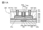
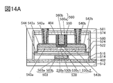
- 14A and 14B are schematic cross-sectional views each illustrating a structural example of a transistor.
- FIG. 15 is a schematic sectional view illustrating a configuration example of a semiconductor device.
- 16A and 16B are schematic cross-sectional views each illustrating a structural example of a transistor.
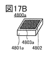
- 17A and 17B are perspective views showing an example of a semiconductor wafer.
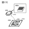
- FIG. 17C and 17D are perspective views showing an example of an electronic component.
- FIG. 18 is a perspective view and a schematic diagram illustrating an example of a product.
- FIG. 19 is a circuit diagram showing the configuration of the semiconductor device according to the example.
- 20A and 20B are graphs showing simulation results of the example.
- FIG. 21 is a circuit diagram showing the configuration of the semiconductor device according to the example.
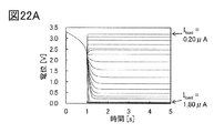
- 22A to 22C are graphs showing simulation results of the example.
- the position, size, range, etc. of each configuration shown in the drawings and the like may not represent the actual position, size, range, etc. in order to facilitate understanding of the invention. Therefore, the disclosed invention is not necessarily limited to the position, size, range, or the like disclosed in the drawings and the like.
- a resist mask or the like may be unintentionally reduced due to a process such as etching, but it may not be reflected in the drawings for easy understanding.
- a top view also referred to as a “plan view”
- a perspective view and the like, some of the constituent elements may be omitted for easy understanding of the drawing.
- electrode and “wiring” do not functionally limit these components.
- electrode may be used as part of “wiring” and vice versa.
- electrode and wiring include the case where a plurality of “electrodes” and “wirings” are integrally formed.
- the resistance value of “resistance” may be determined depending on the length of wiring.
- the resistance value may be determined by connecting to a conductive layer having a resistivity different from that of the conductive layer used for the wiring.
- the resistance value may be determined by doping the semiconductor layer with an impurity.
- a “terminal” in an electric circuit refers to a portion where input or output of current or voltage and reception or transmission of a signal are performed. Therefore, part of the wiring or the electrode may function as a terminal.
- electrode B on insulating layer A it is not necessary that the electrode B is directly formed on the insulating layer A, and another structure is provided between the insulating layer A and the electrode B. Do not exclude those that contain elements.
- the functions of the source and the drain are switched with each other depending on operating conditions such as the case where a transistor having different polarities is adopted, the direction of current changes in circuit operation, and the like, which limits which is a source or a drain. Is difficult. Therefore, in this specification and the like, the terms source and drain can be used interchangeably.
- “electrically connected” includes a case of being directly connected and a case of being connected through “thing having some electric action”.
- the “object having some kind of electrical action” is not particularly limited as long as it can transfer an electric signal between the connection targets. Therefore, even in the case of being expressed as “electrically connected”, there is a case where the actual circuit does not have a physical connection portion and only the wiring extends. Further, even when it is expressed as “direct connection”, it includes a case where different conductive layers are connected via a contact. Note that there are cases where the wiring has different conductive layers containing one or more same elements and cases where the wiring contains different elements.
- the voltage often indicates a potential difference between a certain potential and a reference potential (for example, a ground potential or a source potential). Therefore, the voltage and the potential can be paraphrased in many cases. In this specification and the like, voltage and potential can be paraphrased unless otherwise specified.
- semiconductor even when described as “semiconductor”, for example, when the conductivity is sufficiently high, it has characteristics as “conductor”. Therefore, it is possible to replace the “semiconductor” with the “conductor” and use it. In this case, the boundary between the “semiconductor” and the “conductor” is ambiguous, and it is difficult to strictly distinguish the two. Therefore, the “semiconductor” and the “conductor” described in this specification and the like may be interchangeable in some cases.
- ordinal numbers such as “first” and “second” in this specification and the like are given to avoid confusion among components and do not indicate any order or order such as a process order or a stacking order. .. Further, even in the present specification, a term without an ordinal number may have an ordinal number in the claims in order to avoid confusion among components. Further, even if a term is given an ordinal number in this specification, a different ordinal number may be attached in the claims. Further, even if a term has an ordinal number in this specification, the ordinal number may be omitted in the claims and the like.
- the “on state” of a transistor refers to a state where the source and drain of the transistor can be regarded as being electrically short-circuited (also referred to as “conduction state”). Further, the “off state” of a transistor refers to a state where the source and drain of the transistor can be considered to be electrically disconnected (also referred to as a “non-conduction state”).
- the “on-state current” may refer to a current flowing between the source and the drain when the transistor is on.
- the “off current” may mean a current flowing between the source and the drain when the transistor is off.
- a gate refers to part or all of a gate electrode and a gate wiring.
- a gate wiring refers to a wiring for electrically connecting a gate electrode of at least one transistor to another electrode or another wiring.
- a source refers to part or all of a source region, a source electrode, and a source wiring.
- the source region refers to a region of the semiconductor layer whose resistivity is equal to or lower than a certain value.
- the source electrode refers to a conductive layer in a portion connected to the source region.
- a source wiring refers to a wiring for electrically connecting a source electrode of at least one transistor to another electrode or another wiring.
- a drain refers to part or all of a drain region, a drain electrode, and a drain wiring.
- the drain region refers to a region of the semiconductor layer whose resistivity is equal to or lower than a certain value.
- the drain electrode refers to a conductive layer in a portion connected to the drain region.
- the drain wiring refers to a wiring for electrically connecting the drain electrode of at least one transistor to another electrode or another wiring.
- the metal oxide is a metal oxide in a broad sense. Metal oxides are classified into oxide insulators, oxide conductors (including transparent oxide conductors), oxide semiconductors (Oxide Semiconductor or simply OS), and the like. For example, when a metal oxide is used for a semiconductor layer of a transistor, the metal oxide may be referred to as an oxide semiconductor. That is, the term “OS transistor” can be rephrased as a transistor including a metal oxide or an oxide semiconductor.
- metal oxides containing nitrogen may be collectively referred to as metal oxides. Further, the metal oxide containing nitrogen may be referred to as a metal oxynitride.
- One embodiment of the present invention is a semiconductor device in which a holding transistor is provided between a control circuit and an output transistor.
- the control circuit can have a configuration including an operational amplifier.
- the semiconductor device of one embodiment of the present invention can be applied to a semiconductor device having a function of continuously outputting a constant potential, such as a DC-DC converter, for example, a linear regulator.
- the constant potential can be output from the source or the drain of the output transistor.
- a node where the other of the source and the drain of the holding transistor and the gate of the output transistor are electrically connected is a holding node.
- the holding transistor When the holding transistor is turned on, the potential corresponding to the potential output from the control circuit is written in the holding node. After that, when the holding transistor is turned off, the potential of the holding node is held. Therefore, even if the control circuit is turned off, the gate potential of the output transistor can be maintained at a constant value. Therefore, even if the control circuit is turned off, a constant potential can be continuously output from, for example, the source or drain of the output transistor.
- the self-consumption current which is a current consumed in the control circuit and the like can be reduced, so that the power consumption of the semiconductor device of one embodiment of the present invention can be reduced.
- the holding transistor is preferably a transistor with extremely low off-state current, such as an OS transistor. Accordingly, the potential can be held at the holding node for a long time. Therefore, the frequency of writing the potential to the holding node can be reduced, so that power consumption of the semiconductor device of one embodiment of the present invention can be reduced.
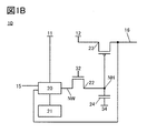
- FIG. 1A is a diagram illustrating a configuration example of a semiconductor device 10 which is a semiconductor device of one embodiment of the present invention.
- the semiconductor device 10 includes a control circuit 20, a power switch circuit 21, a transistor 22, and a transistor 23.
- the transistor 22 can be provided between the control circuit 20 and the transistor 23.
- the control circuit 20 can be configured to have, for example, a first power supply terminal, a second power supply terminal, a first input terminal, a second input terminal, and an output terminal.
- the first power supply terminal of the control circuit 20 can be electrically connected to the wiring 11.
- the second power supply terminal of the control circuit 20 can be electrically connected to the power supply switch circuit 21.
- the first input terminal of the control circuit 20 can be electrically connected to the wiring 15.
- the second input terminal of the control circuit 20 can be electrically connected to the wiring 16.
- the output terminal of the control circuit 20 can be electrically connected to one of the source and the drain of the transistor 22.
- a node NW where the output terminal of the control circuit 20 and one of the source and the drain of the transistor 22 are electrically connected.
- first power supply terminal and “second power supply terminal” can be replaced with each other as necessary or appropriate.
- the wiring 11 may be electrically connected to the second power supply terminal of the control circuit 20, and the power supply switch circuit 21 may be electrically connected to the first power supply terminal of the control circuit 20.
- first input terminal and the term “second input terminal” can be replaced with each other as necessary or appropriate.
- the wiring 15 may be electrically connected to the second input terminal of the control circuit 20, and the wiring 16 may be electrically connected to the first input terminal of the control circuit 20.
- the wiring 16 is electrically connected to the second input terminal of the control circuit 20 and one of a source and a drain of the transistor 23.
- the other of the source and the drain of the transistor 22 is electrically connected to the gate of the transistor 23. Further, the other of the source and the drain of the transistor 23 is electrically connected to the wiring 12.
- a node where the other of the source and the drain of the transistor 22 and the gate of the transistor 23 are electrically connected is a node NH.
- the wiring 11 and the wiring 12 have a function as a power supply line.
- the potentials of the wiring 11 and the wiring 12 can be, for example, high potential.
- a high potential refers to a potential higher than a low potential.
- the low potential is the ground potential
- the positive potential can be the high potential.
- the source potential is low and the potential of the transistor is on when it is applied to the gate of the n-channel transistor, it can be high and the off potential can be low.
- the potential can be high and the potential on can be low.
- the wiring 16 has a function as an output line that outputs a desired potential to the outside of the semiconductor device 10.
- the wiring 16 can be electrically connected to, for example, a device provided outside the semiconductor device 10.
- the control circuit 20 has a function of outputting a potential corresponding to the potential supplied to the input terminal from the output terminal.
- the wiring 16 electrically connected to the second input terminal has a function as an output line. Therefore, it can be said that the control circuit 20 is feedback-controlled. Accordingly, the control circuit 20 can output a potential corresponding to the potential of the wiring 15 electrically connected to the first input terminal.
- the potential of the wiring 15 can be referred to as a reference potential, for example.
- the power switch circuit 21 can control ON/OFF of the control circuit 20 by controlling a current or a potential supplied to the control circuit 20.
- the control circuit 20 being turned on means that the control circuit 20 can output a desired potential
- the control circuit 20 being turned off means that the control circuit 20 is turned off. Is not in a state capable of outputting a desired potential.
- the control circuit 20 when the control circuit 20 is on, the control circuit 20 outputs a potential corresponding to the potential of the wiring 15, and when the control circuit 20 is off, the control circuit 20 outputs the potential.
- the potential is a potential that does not correspond to the potential of the wiring 15.
- the transistor 22 has a function of controlling writing of a potential to the node NH. Specifically, the potential output from the control circuit 20 is written to the node NH when the transistor 22 is on, and the potential of the node NH is held when the transistor 22 is off. To be done. That is, it can be said that the transistor 22 is a holding transistor.
- the transistor 22 it is preferable to use a transistor having extremely low off-state current. Accordingly, the period in which the potential can be held at the node NH can be extremely extended.
- An OS transistor can be given as a transistor having extremely low off-state current. Specifically, the off-state current per 1 ⁇ m of the channel width can be less than 1 ⁇ 10 ⁇ 20 A, preferably less than 1 ⁇ 10 ⁇ 22 A, and more preferably less than 1 ⁇ 10 ⁇ 24 A at room temperature.
- the OS transistor has excellent electrical characteristics in a high temperature environment as compared with a transistor including silicon in a semiconductor layer (hereinafter also referred to as a Si transistor). Therefore, by using an OS transistor as a transistor included in the semiconductor device of one embodiment of the present invention, such as the transistor 22, a semiconductor device with stable operation even in a high temperature environment and favorable reliability can be realized.
- the transistor 23 has a function of outputting a potential corresponding to the potential of the node NH to the wiring 16. That is, the transistor 23 can be said to be an output transistor.
- the transistor 23 can be, for example, a p-channel transistor.
- the transistor 23 can be, for example, a Si transistor. Besides the transistor 23, a Si transistor can be used as a transistor included in the semiconductor device 10.
- the potential output from the control circuit 20 can be a potential corresponding to the potential of the wiring 15 and the potential output from the control circuit 20 is written and held in the node NH. Then, the potential of the wiring 16 becomes a potential corresponding to the potential of the node NH. From the above, the potential of the wiring 16 can be a potential corresponding to the potential of the wiring 15. For example, the potential of the wiring 16 can be the same as or substantially the same as the potential of the wiring 15.
- the semiconductor device 10 by turning on the control circuit 20 and turning on the transistor 22, the potential output from the control circuit 20 is written to the node NH. After that, the transistor 22 is turned off and the potential of the node NH is held, so that the semiconductor device 10 can continue to output a desired potential from the wiring 16 even when the control circuit 20 is turned off.
- the self-consumption current which is a current consumed inside the control circuit 20 and the like, can be reduced, so that the power consumption of the semiconductor device 10 can be reduced.
- the semiconductor device 10 can be applied to, for example, a semiconductor device having a function of continuously outputting a constant potential.
- the semiconductor device 10 can be applied to a DC-DC converter, a linear regulator, or the like.
- FIG. 1B is a modified example of the semiconductor device 10 having the configuration shown in FIG. 1A, and is different from the semiconductor device 10 having the configuration shown in FIG. 1A in that a capacitor 24 is provided.
- the capacitance value of the capacitive element 24 can be, for example, 100 aF or more and 100 pF or less, for example, 10 fF or more and 50 pF or less, and can be 100 fF or more and 10 pF or less, for example, 1 pF or more and 5 pF or less.
- One electrode of the capacitor 24 is electrically connected to the node NH.
- the other electrode of the capacitor 24 is electrically connected to the wiring 34.
- the wiring 34 has a function as a power supply line.
- the potential of the wiring 34 can be, for example, low potential, for example, ground potential.
- the amount of charge that can be held in the node NH can be increased. Therefore, the potential of the node NH can be held for a long time.
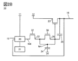
- FIG. 2A is a modified example of the semiconductor device 10 having the configuration shown in FIG. 1B, and is different from the semiconductor device 10 having the configuration shown in FIG. 1B in that it has a transistor 26.
- the transistor 22, the capacitor 24, and the transistor 26 can be provided between the control circuit 20 and the transistor 23.
- the source and the drain of the transistor 26 are electrically connected to the node NH.
- the gate of the transistor 26 is electrically connected to the wiring 36.
- the transistor 26 when the transistor 22 is turned on, the transistor 26 is turned off, and when the transistor 22 is turned off, the transistor 26 is turned on. Accordingly, when the transistor 22 is turned off, the potential of the node NH can be prevented from changing due to capacitive coupling of the capacitor 24 and the like. Therefore, the fluctuation of the potential of the wiring 16 can be suppressed, and the semiconductor device 10 can be stably operated.
- the semiconductor device 10 when the semiconductor device 10 is applied to a DC-DC converter, a linear regulator, or the like, it is preferable that the potential of the node NH does not fluctuate as much as possible because the output potential of the semiconductor device 10 requires high accuracy. Therefore, particularly when the semiconductor device 10 is applied to a DC-DC converter, a linear regulator, or the like, it is preferable to provide the transistor 26 in the semiconductor device 10.
- FIG. 2B is a modification of the semiconductor device 10 having the configuration shown in FIG. 2A, and is different from the semiconductor device 10 having the configuration shown in FIG. 2A in that the capacitor 28 is provided.
- the capacitance value of the capacitive element 28 can be, for example, greater than or equal to the capacitance value of the capacitive element 24.
- One electrode of the capacitor 28 is electrically connected to the node NH, and the other electrode of the capacitor 28 is electrically connected to the wiring 16.
- the potential of the wiring 16 decreases as the potential of the node NH increases, and the potential of the wiring 16 decreases as the potential of the node NH decreases. growing. Therefore, when the semiconductor device 10 is provided with the capacitance element 28, when the potential of one electrode of the capacitance element 28 increases, the potential of the other electrode of the capacitance element 28 increases and when the potential of one electrode of the capacitance element 28 decreases. The potential of the other electrode of the capacitor 28 becomes smaller. Therefore, the change in the potential of the wiring 16 due to the change in the potential of the node NH can be offset.
- the capacitor 28 can have a function similar to that of the capacitor 24. That is, it has a function of holding the potential of the node NH, for example. Therefore, when the semiconductor device 10 has the capacitive element 28, the semiconductor device 10 can be configured without the capacitive element 24. Alternatively, the capacitance value of the capacitive element 24 can be reduced.
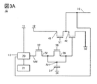
- FIG. 3A is a modified example of the semiconductor device 10 having the configuration shown in FIG. 2A, and is different from the semiconductor device 10 having the configuration shown in FIG. 2A in that the transistor 23 is not provided and the transistors 41 and 42 are provided. As illustrated in FIG. 3A, the transistor 22, the capacitor 24, and the transistor 26 can be provided between the control circuit 20 and the transistor 42.
- One of a source and a drain of the transistor 41 is electrically connected to the wiring 12.
- the other of the source and the drain of the transistor 41 and one of the source and the drain of the transistor 42 are electrically connected to the wiring 16.
- the other of the source and the drain of the transistor 42 is electrically connected to the wiring 52.
- the gate of the transistor 41 is electrically connected to the wiring 51.
- the gate of the transistor 42 is electrically connected to the node NH.
- a bias potential can be supplied to the wiring 51.
- the bias potential may be a constant potential, for example.
- the transistor 41 can function as a current source.
- the wiring 52 also has a function as a power supply line.
- the potential of the wiring 52 can be low potential, for example, ground potential.
- the transistors 41 and 42 can be, for example, n-channel transistors.
- the potential of the wiring 12 is high and the potential of the wiring 52 is low
- the transistors 41 and 42 are n-channel transistors
- the potential of the wiring 16 decreases and the potential of the node NH decreases as the potential of the node NH increases.
- the potential of the wiring 16 increases. That is, even if the p-channel type transistor is not used as the output transistor, the semiconductor device 10 can perform, for example, the same operation as when the p-channel type transistor is used as the output transistor.
- OS transistors can be used as the transistors 41 and 42.
- the OS transistor has superior electrical characteristics in a high temperature environment as compared with the Si transistor. Therefore, by using OS transistors as the transistors 41 and 42, the potential of the wiring 16 is stable even in a high temperature environment. Therefore, the potential output from the semiconductor device 10 is stable even in a high temperature environment, and the semiconductor device 10 can be operated stably.
- FIG. 3B is a modified example of the semiconductor device 10 having the configuration shown in FIG. 3A, and is different from the semiconductor device 10 having the configuration shown in FIG. 3A in that a capacitor 28 is provided. 2B, one electrode of the capacitor 28 is electrically connected to the node NH, and the other electrode of the capacitor 28 is electrically connected to the wiring 16.
- the semiconductor device 10 By configuring the semiconductor device 10 as shown in FIG. 3B, the semiconductor device 10 can be stably operated as in the case where the semiconductor device 10 is configured as shown in FIG. 2B.
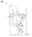
- FIG. 4 is a circuit diagram showing a specific configuration example of the semiconductor device 10 shown in FIG. 2A.
- FIG. 4 shows a circuit configuration example of the control circuit 20 and the power switch circuit 21.
- the control circuit 20 has an operational amplifier circuit 40.
- the power switch circuit 21 includes a transistor 44a, a transistor 44b, and a current source 45.
- the operational amplifier circuit 40 can be configured to have, for example, a first power supply terminal, a second power supply terminal, a first input terminal, a second input terminal, and an output terminal.
- the first and second power supply terminals, the first and second input terminals, and the output terminal of the operational amplifier circuit 40 are respectively connected to the first and second power supply terminals, the first and second input terminals of the control circuit 20, respectively. It can be a terminal or an output terminal.
- the first power supply terminal of the operational amplifier circuit 40 is electrically connected to the wiring 11.
- the second power supply terminal of the operational amplifier circuit 40 is electrically connected to one of the source and drain of the transistor 44a and one of the source and drain of the transistor 44b.
- a node to which the second power supply terminal of the operational amplifier circuit 40, one of the source and the drain of the transistor 44a, and one of the source and the drain of the transistor 44b are electrically connected is a node Nref.
- the first input terminal of the operational amplifier circuit 40 is electrically connected to the wiring 15.
- the second input terminal of the operational amplifier circuit 40 is electrically connected to the wiring 16.
- FIG. 4 shows a case where the non-inverting input terminal is the first input terminal of the operational amplifier circuit 40 and the inverting input terminal is the second input terminal of the operational amplifier circuit 40.
- the output terminal of the operational amplifier circuit 40 is electrically connected to the node NW.
- the other of the source and the drain of the transistor 44a is electrically connected to one electrode of the current source 45.
- the gate of the transistor 44a is electrically connected to the wiring 54a.
- the other electrode of the current source 45 is electrically connected to the wiring 55a.
- the other of the source and the drain of the transistor 44b is electrically connected to the wiring 55b.
- the gate of the transistor 44b is electrically connected to the wiring 54b.
- the wiring 55a and the wiring 55b function as a power supply line.
- the potentials of the wiring 55a and the wiring 55b can be low potential, for example, ground potential.
- the operational amplifier circuit 40 is turned on by turning on the transistor 44a and turning off the transistor 44b. Therefore, the operational amplifier circuit 40 can output a potential corresponding to the potential of the wiring 15, for example. On the other hand, when the transistor 44a is turned off and the transistor 44b is turned on, the operational amplifier circuit 40 is turned off. Therefore, the operational amplifier circuit 40 can stop the output of the potential, for example. Details of switching on/off of the operational amplifier circuit 40 will be described later.
- FIG. 5 is a modification of the semiconductor device 10 having the configuration shown in FIG. 4, and is different from the semiconductor device 10 having the configuration shown in FIG. 4 in that the transistor 23 is an n-channel transistor.
- the wiring 15 can be electrically connected to the inverting input terminal of the operational amplifier circuit 40, and the wiring 16 can be electrically connected to the non-inverting input terminal of the operational amplifier circuit 40.
- the transistor 23 When the transistor 23 is an n-channel transistor, the transistor 23 can be an OS transistor. As described above, the OS transistor has superior electrical characteristics in a high temperature environment as compared with the Si transistor. Therefore, by using an OS transistor as the transistor 23, the potential of the wiring 16 is stable even in a high temperature environment. Therefore, the potential output from the semiconductor device 10 is stable even in a high temperature environment, and the semiconductor device 10 can be operated stably.
- FIG. 6 is a circuit diagram showing a specific configuration example of the semiconductor device 10 shown in FIG. 4, and shows a circuit configuration example of the operational amplifier circuit 40.
- the operational amplifier circuit 40 includes a transistor 63a, a transistor 63b, a transistor 64a, a transistor 64b, a transistor 65a, and a transistor 65b.
- One of a source and a drain of the transistor 63a and one of a source and a drain of the transistor 63b are electrically connected to the wiring 11.
- the other of the source and the drain of the transistor 63a is electrically connected to one of the source and the drain of the transistor 64a.
- One of a source and a drain of the transistor 64a is electrically connected to one of a source and a drain of the transistor 22.
- the gate of the transistor 63a is electrically connected to the gate of the transistor 63b.
- the gate of the transistor 63b is electrically connected to the other of the source and the drain of the transistor 63b.
- the other of the source and the drain of the transistor 63b is electrically connected to one of the source and the drain of the transistor 64b.
- the other of the source and the drain of the transistor 64a and the other of the source and the drain of the transistor 64b are electrically connected to one of the source and the drain of the transistor 65a.
- the other of the source and the drain of the transistor 65a is electrically connected to the wiring 75a.
- the gate of the transistor 65a, the gate of the transistor 65b, and one of the source and the drain of the transistor 65b are electrically connected to the node Nref.
- the other of the source and the drain of the transistor 65b is electrically connected to the wiring 75b.
- the gate of the transistor 64a is electrically connected to the wiring 15 and the gate of the transistor 64b is electrically connected to the wiring 16. That is, the gate of the transistor 64a can be said to be the first input terminal of the operational amplifier circuit 40, and the gate of the transistor 64b can be said to be the second input terminal of the operational amplifier circuit 40.
- the wiring 75a and the wiring 75b function as a power supply line.
- the potential of the wiring 75a and the wiring 75b can be low potential, for example, ground potential.
- FIG. 7 is a modification of the semiconductor device 10 having the configuration shown in FIG. 6, and is different from the semiconductor device 10 having the configuration shown in FIG. As in the case shown in FIG. 2B, one electrode of the capacitor 28 is electrically connected to the node NH, and the other electrode of the capacitor 28 is electrically connected to the wiring 16.
- the semiconductor device 10 By configuring the semiconductor device 10 to have the capacitive element 28, the semiconductor device 10 can be stably operated as described above.
- FIG. 8 is a timing chart showing an example of an operating method of the semiconductor device 10 having the configuration shown in FIG. In FIG. 8, “H” indicates a high potential and “L” indicates a low potential. Note that in the following description, the potentials of the wiring 11 and the wiring 12 are high potentials. The potentials of the wiring 34, the wiring 55a, the wiring 55b, the wiring 75a, and the wiring 75b are low.
- the potential of the wiring 32 is low, the potential of the wiring 36 is high, the potential of the wiring 54a is low, and the potential of the wiring 54b is high.
- the transistor 22 is off, the transistor 26 is on, the transistor 44a is off, and the transistor 44b is on.
- the potential of the node Nref is low, so that no current flows through the transistor 65b and thus no current flows through the transistor 65a. Therefore, it can be said that the operational amplifier circuit 40 is off.
- the potential of the wiring 32 is low, the potential of the wiring 36 is high, the potential of the wiring 54a is high, and the potential of the wiring 54b is low.
- the transistor 22 is turned off, the transistor 26 is turned on, the transistor 44a is turned on, and the transistor 44b is turned off.
- the transistor 44a is turned on, a current flows from the current source 45 toward the node Nref, so that the potential of the node Nref rises.
- a current flows between the source and the drain of the transistor 65b.
- a current mirror is formed by the transistors 65a and 65b, current also flows through the transistor 65a. Therefore, a current flows between the wiring 11 and the wirings 75a and 75b, and the operational amplifier circuit 40 is turned on.
- the operational amplifier circuit 40 is turned off when the potential of the node Nref is low, and the operational amplifier circuit 40 is turned on when the potential of the node Nref is higher than the low potential.
- the potential of the wiring 32 is high, the potential of the wiring 36 is low, the potential of the wiring 54a is high, and the potential of the wiring 54b is low.
- the transistor 22 is turned on, the transistor 26 is turned off, the transistor 44a is turned on, and the transistor 44b is turned off.
- the potential of the wiring 16 becomes a potential corresponding to the potential of the node NH which is the gate potential of the transistor 23.
- the potential of the node NH can be a potential corresponding to the potential of the wiring 15.
- the potential of the wiring 16 becomes a potential corresponding to the potential of the wiring 15. Note that in FIG. 8, the potential of the node NH from time T2 to time T3 is equal to the potential of the node NW which is a node to which the output terminal of the control circuit 20 is electrically connected.
- the potential of the wiring 32 is low, the potential of the wiring 36 is high, the potential of the wiring 54a is high, and the potential of the wiring 54b is low.
- the transistor 22 is turned off, the transistor 26 is turned on, the transistor 44a is turned on, and the transistor 44b is turned off. With the transistor 22 turned off and the transistor 26 turned on, the potential of the node NH is held.
- the potential of the wiring 32 is low, the potential of the wiring 36 is high, the potential of the wiring 54a is low, and the potential of the wiring 54b is high.
- the transistor 22 is turned off, the transistor 26 is turned on, the transistor 44a is turned off, and the transistor 44b is turned on. Since the transistor 44a is turned off and the transistor 44b is turned on, the potential of the node Nref becomes low and current does not flow between the source and the drain of the transistor 65b. Accordingly, current does not flow between the source and the drain of the transistor 65a, so that the potential of one of the source and the drain of the transistor 65a approaches a high potential which is the potential of the wiring 11.
- the potential of the wiring 75a is low and lower than the potential of the wiring 11, so that the potential of one of the source and the drain of the transistor 65a increases. As a result, the potential of the node NW rises. As described above, the operational amplifier circuit 40 is turned off.
- the transistor 22 since the transistor 22 is off, the potential of the node NH does not vary even if the potential of the node NW varies. Therefore, even from time T4 to time T5 when the operational amplifier circuit 40 is off, the potential of the wiring 16 does not change from the potential from time T2 to time T4 when the operational amplifier circuit 40 is on.
- the potential of the node NW rises and the potential of the node NH does not change. Therefore, when the transistor 22 is an n-channel transistor, the source of the transistor 22 is electrically connected to the node NH. It will be composed. Therefore, when the potential to be written to the node NH is increased from time T2 to time T3, the difference between the gate potential of the transistor 22 and the source potential of the transistor 22 is small (the difference is a negative value when the transistor 22 is turned off). In some cases, the absolute value of the difference is large). Thus, the off-state current of the transistor 22 is reduced, so that the potential of the node NH can be held for a long time.
- the difference between the gate potential of the transistor 22 and the source potential of the transistor 22 is negative. Therefore, when the gate potential of the transistor 22 is equal to the source potential of the transistor 22, for example, the off-state current of the transistor 22 is smaller than when the gate potential of the transistor 22 and the source potential of the transistor 22 are both ground potential, and the potential of the node NH Can be held for a long time.
- the operational amplifier circuit 40 can be turned off after the operational amplifier circuit 40 is turned on and the potential is written in the node NH again.
- the above is an example of the operation method of the semiconductor device 10.
- the potential of the wiring 36 is high while the potential of the wiring 32 is low, and the potential of the wiring 36 is high while the potential of the wiring 32 is high.
- the potential is low. That is, it can be said that signals complementary to each other are supplied to the wiring 32 and the wiring 36.
- the potential of the wiring 54b is high while the potential of the wiring 54a is low, and the potential of the wiring 54b is low while the potential of the wiring 54a is high. There is. That is, it can be said that signals complementary to each other are supplied to the wiring 54a and the wiring 54b. Note that there may be a period in which both the wiring 32 and the wiring 36 have a low potential or a period in which both the wiring 32 and the wiring 36 have a high potential.
- both the wiring 54a and the wiring 54b may have a low potential, or a period in which both the wiring 54a and the wiring 54b have a high potential.
- both the wiring 32 and the wiring 36 may have a high potential or a low potential during a period within 20% of time T1 to time T5.
- both the wiring 54a and the wiring 54b may have a high potential or a low potential in a period within 20% of the time T1 to the time T5.
- the semiconductor device 10 can continue to output a desired potential even when the operational amplifier circuit 40 is turned off. As described above, when the operational amplifier circuit 40 is turned off, no current flows in the transistors 65a and 65b. Therefore, the self-power consumption can be reduced by operating the semiconductor device 10 by the method shown in FIG. 8, so that the power consumption of the semiconductor device 10 can be reduced.
- the transistor 22 is preferably a transistor with extremely low off-state current, such as an OS transistor. Accordingly, the potential can be kept held at the node NH for a long time, so that the period from time T4 to time T5 can be extended. Therefore, the frequency of writing the potential to the node NH can be reduced. That is, it is possible to reduce the frequency of performing the operations shown from time T1 to time T4. As a result, the power consumption of the semiconductor device 10 can be reduced.
- the semiconductor device 10 can be applied to a DC-DC converter, a linear regulator, or the like. These require high precision in the output potential.
- the transistor 22 can be a transistor with extremely low off-state current such as an OS transistor.
- the semiconductor device 10 is operated by the method shown in FIG. 8, as described above, when the transistor 22 is turned off, the difference between the gate potential of the transistor 22 and the source potential of the transistor 22 is small (the difference is negative). The absolute value of the difference becomes large).
- the semiconductor device 10 can continue to output the potential with high accuracy, and the semiconductor device 10 can be stably operated.
- This embodiment can be implemented in appropriate combination with any of the structures described in the other embodiments and the like.
- the semiconductor device illustrated in FIG. 9 includes a transistor 300, a transistor 500, and a capacitor 600.
- 11A is a cross-sectional view of the transistor 500 in the channel length direction
- FIG. 11B is a cross-sectional view of the transistor 500 in the channel width direction
- FIG. 11C is a cross-sectional view of the transistor 300 in the channel width direction.
- the transistor 500 is an OS transistor.
- the off-state current of the transistor 500 is small. Therefore, for example, when the structure of the transistor 22 described in the above embodiment is similar to that of the transistor 500, the potential can be held at the node NH for a long time. Thus, the frequency of writing the potential to the node NH is reduced, so that power consumption of the semiconductor device can be reduced.
- the semiconductor device described in this embodiment includes a transistor 300, a transistor 500, and a capacitor 600 as illustrated in FIG.
- the transistor 500 is provided above the transistor 300
- the capacitor 600 is provided above the transistor 300 and the transistor 500.
- the transistor 23 described in the above embodiment can have a structure similar to that of the transistor 300
- the capacitor 24 can have a structure similar to that of the capacitor 600.
- the transistor 300 is provided over the substrate 311.
- the transistor 300 includes a conductor 316 and an insulator 315. Further, the transistor 300 includes a semiconductor region 313 formed of a part of the substrate 311, a low resistance region 314a which functions as a source region or a drain region, and a low resistance region 314b.
- the top surface of the semiconductor region 313 and the side surface in the channel width direction are covered with the conductor 316 with the insulator 315 interposed therebetween.
- the Fin type transistor 300 increases the effective channel width. Accordingly, the on characteristics of the transistor 300 can be improved. Further, since the electric field contribution of the gate electrode can be increased, the off characteristics of the transistor 300 can be improved.
- the transistor 300 may be either a p-channel type or an n-channel type.
- a region of the semiconductor region 313 in which a channel is formed, a region in the vicinity thereof, a low-resistance region 314a and a low-resistance region 314b which serve as a source region or a drain region, and the like preferably contain a semiconductor such as a silicon-based semiconductor, and a single crystal. It preferably contains silicon. Alternatively, a material including Ge (germanium), SiGe (silicon germanium), GaAs (gallium arsenide), GaAlAs (gallium aluminum arsenide), or the like may be used. A structure may be used in which silicon is used in which the effective mass is controlled by applying stress to the crystal lattice and changing the lattice spacing. Alternatively, the transistor 300 may be a HEMT (High Electron Mobility Transistor) by using GaAs and GaAlAs.
- HEMT High Electron Mobility Transistor
- the low-resistance region 314a and the low-resistance region 314b impart an n-type conductivity imparting element such as arsenic or phosphorus, or a p-type conductivity imparting boron, in addition to the semiconductor material applied to the semiconductor region 313. Including the element to do.
- the conductor 316 functioning as a gate electrode can be formed using a semiconductor material such as silicon containing an element imparting n-type conductivity such as arsenic or phosphorus, or an element imparting p-type conductivity such as boron. ..
- a conductive material such as a metal material, an alloy material, or a metal oxide material can be used.
- the threshold voltage of the transistor can be adjusted by selecting the material of the conductor. Specifically, it is preferable to use a material such as titanium nitride or tantalum nitride for the conductor. Further, in order to achieve both conductivity and embedding properties, it is preferable to stack and use a metal material such as tungsten or aluminum on the conductor, and it is particularly preferable to use tungsten in terms of heat resistance.
- the structure of the transistor 300 illustrated in FIG. 9 is an example, and the structure is not limited thereto, and an appropriate transistor may be used depending on a circuit structure or an operation method.
- the transistor 300 may have a structure similar to that of the transistor 500 which is an OS transistor as illustrated in FIG. Note that details of the transistor 500 will be described later.
- the transistor 300 illustrated in FIG. 10 can be applied to the n-channel transistor 23 illustrated in FIG. 5, for example.
- a unipolar circuit refers to a circuit in which all transistors are transistors of the same polarity, for example.
- a circuit in which all transistors are n-channel transistors can be said to be a unipolar circuit.
- An insulator 320, an insulator 322, an insulator 324, and an insulator 326 are sequentially stacked to cover the transistor 300.
- the insulator 320, the insulator 322, the insulator 324, and the insulator 326 for example, silicon oxide, silicon oxynitride, silicon nitride oxide, silicon nitride, aluminum oxide, aluminum oxynitride, aluminum nitride oxide, aluminum nitride, or the like is used. Good.
- silicon oxynitride refers to a material whose content of oxygen is higher than that of nitrogen
- silicon oxynitride is a material whose content of nitrogen is higher than that of oxygen.
- aluminum oxynitride refers to a material having a higher oxygen content than nitrogen as its composition
- aluminum oxynitride means a material having a higher nitrogen content than oxygen as its composition.
- the insulator 322 may have a function as a planarization film which planarizes a step formed by the transistor 300 or the like provided below the insulator 322.
- the upper surface of the insulator 322 may be flattened by a flattening treatment using a chemical mechanical polishing (CMP) method or the like in order to improve flatness.
- CMP chemical mechanical polishing
- the insulator 324 it is preferable to use a film having a barrier property such that hydrogen and impurities do not diffuse from the substrate 311, the transistor 300, or the like to a region where the transistor 500 is provided.
- a film having a barrier property against hydrogen for example, silicon nitride formed by a CVD method can be used.
- silicon nitride formed by a CVD method when hydrogen diffuses into a semiconductor element including an oxide semiconductor, such as the transistor 500, characteristics of the semiconductor element might be deteriorated in some cases. Therefore, it is preferable to use a film which suppresses diffusion of hydrogen between the transistor 500 and the transistor 300.
- the film that suppresses hydrogen diffusion is a film in which the amount of released hydrogen is small.
- the desorption amount of hydrogen can be analyzed using, for example, a thermal desorption gas analysis method (TDS).
- TDS thermal desorption gas analysis method
- the desorption amount of hydrogen in the insulator 324 is calculated by converting the desorption amount converted into hydrogen atoms into the area of the insulator 324 in the range of the surface temperature of the film from 50° C. to 500° C. Therefore, it may be 10 ⁇ 10 15 atoms/cm 2 or less, preferably 5 ⁇ 10 15 atoms/cm 2 or less.
- the insulator 326 preferably has a lower relative permittivity than the insulator 324.
- the dielectric constant of the insulator 326 is preferably less than 4, and more preferably less than 3.
- the relative dielectric constant of the insulator 326 is preferably 0.7 times or less, and more preferably 0.6 times or less that of the insulator 324.
- a conductor 328, a conductor 330, and the like which are connected to the capacitor 600 or the transistor 500 are embedded.
- the conductor 328 and the conductor 330 have a function as a plug or a wiring.
- the conductor having a function as a plug or a wiring may have a plurality of structures collectively given the same reference numeral. In this specification and the like, the wiring and the plug connected to the wiring may be integrated. That is, part of the conductor may function as a wiring, and part of the conductor may function as a plug.
- a conductive material such as a metal material, an alloy material, a metal nitride material, or a metal oxide material is used as a single layer or a laminated layer. be able to. It is preferable to use a high melting point material such as tungsten or molybdenum, which has both heat resistance and conductivity, and it is preferable to use tungsten. Alternatively, it is preferably formed of a low resistance conductive material such as aluminum or copper. Wiring resistance can be reduced by using a low-resistance conductive material.
- a wiring layer may be provided over the insulator 326 and the conductor 330.
- an insulator 350, an insulator 352, and an insulator 354 are sequentially stacked and provided.
- a conductor 356 is formed over the insulator 350, the insulator 352, and the insulator 354.
- the conductor 356 has a function of a plug connected to the transistor 300 or a wiring. Note that the conductor 356 can be provided using a material similar to that of the conductor 328 or the conductor 330.
- the insulator 350 like the insulator 324, an insulator having a barrier property against hydrogen is preferably used.
- the conductor 356 preferably contains a conductor having a barrier property against hydrogen.
- a conductor having a barrier property against hydrogen be formed in an opening provided in the insulator 350 having a barrier property against hydrogen.
- tantalum nitride or the like is preferably used as the conductor having a barrier property against hydrogen. Further, by stacking tantalum nitride and tungsten having high conductivity, diffusion of hydrogen from the transistor 300 can be suppressed while maintaining conductivity as a wiring. In this case, it is preferable that the tantalum nitride layer having a hydrogen barrier property is in contact with the insulator 350 having a hydrogen barrier property.
- a wiring layer may be provided over the insulator 354 and the conductor 356.
- an insulator 360, an insulator 362, and an insulator 364 are sequentially stacked and provided.
- a conductor 366 is formed over the insulator 360, the insulator 362, and the insulator 364.
- the conductor 366 has a function as a plug or a wiring. Note that the conductor 366 can be provided using a material similar to that of the conductor 328 or the conductor 330.
- the conductor 366 preferably contains a conductor having a barrier property against hydrogen.
- a conductor having a barrier property against hydrogen be formed in an opening portion provided in the insulator 360 having a barrier property against hydrogen.
- a wiring layer may be provided over the insulator 364 and the conductor 366.
- an insulator 370, an insulator 372, and an insulator 374 are sequentially stacked and provided.
- a conductor 376 is formed over the insulator 370, the insulator 372, and the insulator 374.
- the conductor 376 has a function as a plug or a wiring. Note that the conductor 376 can be provided using a material similar to that of the conductor 328 or the conductor 330.
- the conductor 376 preferably includes a conductor having a barrier property against hydrogen.
- a conductor having a barrier property against hydrogen be formed in an opening portion provided in the insulator 370 having a barrier property against hydrogen.
- a wiring layer may be provided over the insulator 374 and the conductor 376.
- an insulator 380, an insulator 382, and an insulator 384 are sequentially stacked and provided.
- a conductor 386 is formed over the insulator 380, the insulator 382, and the insulator 384.
- the conductor 386 has a function as a plug or a wiring. Note that the conductor 386 can be provided using a material similar to that of the conductor 328 or the conductor 330.
- the insulator 380 like the insulator 324, an insulator having a barrier property against hydrogen is preferably used.
- the conductor 386 preferably contains a conductor having a barrier property against hydrogen.
- a conductor having a barrier property against hydrogen be formed in an opening portion provided in the insulator 380 having a barrier property against hydrogen.
- the semiconductor device has been described above, the semiconductor device according to this embodiment It is not limited to this.
- the number of wiring layers similar to the wiring layer including the conductor 356 may be three or less, or the number of wiring layers similar to the wiring layer including the conductor 356 may be five or more.
- An insulator 510, an insulator 512, an insulator 514, and an insulator 516 are sequentially stacked over the insulator 384.
- Any of the insulator 510, the insulator 512, the insulator 514, and the insulator 516 is preferably formed using a substance having a barrier property against oxygen and hydrogen.
- the insulator 510 and the insulator 514 it is preferable to use a film having a barrier property such that hydrogen and impurities do not diffuse from the substrate 311 or the like, or from the region where the transistor 300 is provided to the region where the transistor 500 is provided. .. Therefore, it is preferable to use a material similar to that of the insulator 324.
- silicon nitride formed by a CVD method can be used as an example of a film having a barrier property against hydrogen.
- silicon nitride formed by a CVD method when hydrogen diffuses into a semiconductor element including an oxide semiconductor, such as the transistor 500, characteristics of the semiconductor element might be deteriorated in some cases. Therefore, it is preferable to use a film which suppresses diffusion of hydrogen between the transistor 500 and the transistor 300.
- the film that suppresses the diffusion of hydrogen is specifically a film in which the amount of released hydrogen is small.
- a metal oxide such as aluminum oxide, hafnium oxide, or tantalum oxide is preferably used for the insulator 510 and the insulator 514.
- aluminum oxide has a high blocking effect on both oxygen and impurities such as hydrogen and moisture which cause fluctuations in electrical characteristics of a transistor, which do not pass through the film. Therefore, aluminum oxide can prevent impurities such as hydrogen and moisture from entering the transistor 500 during and after the manufacturing process of the transistor. In addition, release of oxygen from the metal oxide included in the transistor 500 can be suppressed. Therefore, it is suitable to be used as a protective film for the transistor 500.
- the same material as that of the insulator 320 can be used for the insulator 512 and the insulator 516. Further, by applying a material having a relatively low dielectric constant to these insulators, it is possible to reduce the parasitic capacitance generated between the wirings.
- a silicon oxide film, a silicon oxynitride film, or the like can be used as the insulator 512 and the insulator 516.
- a conductor 518 In the insulator 510, the insulator 512, the insulator 514, and the insulator 516, a conductor 518, a conductor included in the transistor 500 (eg, the conductor 503), and the like are embedded. Note that the conductor 518 has a function of a plug connected to the capacitor 600 or the transistor 300, or a wiring.
- the conductor 518 can be provided using a material similar to that of the conductor 328 or the conductor 330.
- the conductor 518 in a region which is in contact with the insulator 510 and the insulator 514 is preferably a conductor having a barrier property against oxygen, hydrogen, and water.
- the transistor 300 and the transistor 500 can be separated by a layer having a barrier property against oxygen, hydrogen, and water, and diffusion of hydrogen from the transistor 300 to the transistor 500 can be suppressed.
- the transistor 500 is provided above the insulator 514.
- the transistor 500 includes a conductor 503 arranged so as to be embedded in an insulator 514 and an insulator 516 and an insulator 520 arranged over the insulator 516 and the conductor 503.
- An insulator 522 arranged on the insulator 520, an insulator 524 arranged on the insulator 522, an oxide 530a arranged on the insulator 524, and an oxide 530a arranged on the oxide 530a.
- the oxide 530b arranged, the conductor 542a and the conductor 542b arranged apart from each other on the oxide 530b, and the conductor 542a and the conductor 542b arranged between the conductor 542a and the conductor 542b.
- An insulator 580 in which an opening is overlapped and formed, an oxide 530c arranged so as to have a region in contact with a bottom surface and a side surface of the opening, an insulator 550 arranged in a formation surface of the oxide 530c, and an insulator. And a conductor 560 arranged on the formation surface of 550.
- the insulator 544 is preferably provided between the oxide 530a, the oxide 530b, the conductor 542a, and the insulator 580 and the insulator 580.
- the conductor 560 includes a conductor 560a provided inside the insulator 550 and a conductor 560b provided so as to be embedded inside the conductor 560a. It is preferable to have.
- an insulator 574 is preferably provided over the oxide 530c, the insulator 580, the conductor 560, and the insulator 550.
- the oxide 530a, the oxide 530b, and the oxide 530c may be collectively referred to as the oxide 530.
- the transistor 500 has a structure in which three layers of an oxide 530a, an oxide 530b, and an oxide 530c are stacked in a region where a channel is formed and in the vicinity thereof, the present invention is not limited to this. Not a thing. For example, a single layer of the oxide 530b, a two-layer structure of the oxide 530b and the oxide 530a, a two-layer structure of the oxide 530b and the oxide 530c, or a stacked structure of four or more layers may be provided. Further, in the transistor 500, the conductor 560 is illustrated as a stacked structure of two layers, but the present invention is not limited to this.
- the conductor 560 may have a single-layer structure or a stacked structure including three or more layers.
- the structure of the transistor 500 illustrated in FIGS. 9, 10, 11A, and 11B is an example, and the structure is not limited thereto, and an appropriate transistor may be used depending on a circuit structure or an operation method.
- the conductor 560 functions as a gate electrode of the transistor 500, and the conductors 542a and 542b function as a source electrode and a drain electrode, respectively.
- the conductor 560 is formed so as to be embedded in the opening of the insulator 580 and the region between the conductor 542a and the conductor 542b.
- the arrangement of the conductor 560, the conductor 542a, and the conductor 542b is selected in a self-aligned manner with respect to the opening of the insulator 580. That is, in the transistor 500, the gate electrode can be arranged in a self-aligned manner between the source electrode and the drain electrode. Therefore, the conductor 560 can be formed without providing a positioning margin, so that the area occupied by the transistor 500 can be reduced. As a result, the semiconductor device can be miniaturized and highly integrated.
- the conductor 560 is formed in a region between the conductor 542a and the conductor 542b in a self-aligned manner, the conductor 560 does not have a region overlapping with the conductor 542a or the conductor 542b. Accordingly, the parasitic capacitance formed between the conductor 560 and the conductors 542a and 542b can be reduced. Therefore, the switching speed of the transistor 500 is improved and high frequency characteristics can be obtained.
- the conductor 560 may function as a first gate (also referred to as a top gate) electrode.
- the conductor 503 may function as a second gate (also referred to as a bottom gate) electrode.
- the threshold voltage of the transistor 500 can be controlled by changing the potential applied to the conductor 503 independently of the potential applied to the conductor 560.
- the threshold voltage of the transistor 500 can be made higher than 0 V and the off-state current can be reduced. Therefore, applying a negative potential to the conductor 503 can reduce the drain current when the potential applied to the conductor 560 is 0 V, as compared to the case where no potential is applied.
- the conductor 503 is arranged so as to have a region overlapping with the oxide 530 and the conductor 560. Thus, when a potential is applied to the conductor 560 and the conductor 503, the electric field generated from the conductor 560 and the electric field generated from the conductor 503 are connected to cover a channel formation region formed in the oxide 530.
- a structure of a transistor in which a channel formation region is electrically surrounded by an electric field of a first gate electrode and a second gate electrode is referred to as a surrounded channel (s-channel) structure.
- the conductor 503 has a structure similar to that of the conductor 518, and the conductor 503a is formed in contact with the inner walls of the openings of the insulator 514 and the insulator 516, and the conductor 503b is formed further inside.
- the transistor 500 has a structure in which the conductor 503a and the conductor 503b are stacked, the present invention is not limited to this.
- the conductor 503 may have a single-layer structure or a stacked structure including three or more layers.
- the conductor 503a it is preferable to use a conductive material having a function of suppressing diffusion of impurities such as hydrogen atoms, hydrogen molecules, water molecules, and copper atoms (the above impurities are less likely to penetrate).
- a conductive material having a function of suppressing diffusion of oxygen eg, at least one of an oxygen atom and an oxygen molecule
- the function of suppressing diffusion of impurities or oxygen is a function of suppressing diffusion of any one or all of the above impurities and oxygen.
- the conductor 503a since the conductor 503a has a function of suppressing diffusion of oxygen, it is possible to prevent the conductor 503b from being oxidized and being reduced in conductivity.
- the conductor 503b is preferably formed using a conductive material having high conductivity, which contains tungsten, copper, or aluminum as its main component. In that case, the conductor 503a does not necessarily have to be provided.
- the conductor 503b is illustrated as a single layer, it may have a laminated structure, for example, a laminate of titanium or titanium nitride and the above conductive material.
- the insulator 520, the insulator 522, and the insulator 524 function as a second gate insulating film.
- the insulator 524 which is in contact with the oxide 530, an insulator containing more oxygen than oxygen which satisfies the stoichiometric composition is preferably used. That is, it is preferable that the insulator 524 be formed with an excess oxygen region. By providing such an insulator containing excess oxygen in contact with the oxide 530, oxygen vacancies in the oxide 530 can be reduced and the reliability of the transistor 500 can be improved.
- an oxide material in which part of oxygen is released by heating is preferably used.
- An oxide that desorbs oxygen by heating means that the amount of desorbed oxygen in terms of oxygen atoms is 1.0 ⁇ 10 18 atoms/cm 3 or more, preferably 1 or more by TDS (Thermal Desorption Spectroscopy) analysis.
- the surface temperature of the film during the TDS analysis is preferably 100° C. or higher and 700° C. or lower, or 100° C. or higher and 400° C. or lower.
- any one or more of heat treatment, microwave treatment, and RF treatment may be performed by contacting the insulator having the excess oxygen region with the oxide 530.
- water or hydrogen in the oxide 530 can be removed.
- reactions occur which bonds VoH is disconnected, when other words by reacting as "V O H ⁇ V O + H" occurs, it is possible to dehydrogenation.
- Part of the hydrogen generated at this time may be combined with oxygen and converted into H 2 O, which is removed from the oxide 530 or the insulator in the vicinity of the oxide 530.
- part of hydrogen may be diffused or captured (also referred to as gettering) in the conductor 542.
- a device having a power source for generating high-density plasma or a device having a power source for applying RF to the substrate side for the microwave treatment.
- a high-density oxygen radical can be generated by using a gas containing oxygen and using high-density plasma.
- oxygen radicals generated by high-density plasma can be efficiently introduced into the oxide 530 or the insulator near the oxide 530.
- the pressure may be 133 Pa or higher, preferably 200 Pa or higher, more preferably 400 Pa or higher.
- oxygen and argon are used, and an oxygen flow rate ratio (O 2 /(O 2 +Ar)) is 50% or less, preferably 10% or more and 30% or less. Good to do.
- heat treatment is preferably performed with the surface of the oxide 530 exposed.
- the heat treatment may be performed at 100 °C to 450 °C inclusive, more preferably 350 °C to 400 °C inclusive, for example.
- the heat treatment is performed in an atmosphere of a nitrogen gas or an inert gas, or an atmosphere containing an oxidizing gas at 10 ppm or more, 1% or more, or 10% or more.
- the heat treatment is preferably performed in an oxygen atmosphere. Accordingly, oxygen can be supplied to the oxide 530 to reduce oxygen vacancies (V 2 O 3 ).
- the heat treatment may be performed under reduced pressure.
- the heat treatment may be performed in an atmosphere containing an oxidizing gas in an amount of 10 ppm or higher, 1% or higher, or 10% or higher in order to supplement desorbed oxygen after the heat treatment is performed in a nitrogen gas or inert gas atmosphere.
- the heat treatment may be performed in an atmosphere containing an oxidizing gas in an amount of 10 ppm or more, 1% or more, or 10% or more, and then continuously performed in a nitrogen gas or inert gas atmosphere.
- the insulator 522 preferably has a function of suppressing diffusion of oxygen (eg, oxygen atoms, oxygen molecules, and the like) (oxygen is difficult to permeate).
- oxygen eg, oxygen atoms, oxygen molecules, and the like
- the insulator 522 have a function of suppressing diffusion of oxygen and impurities because oxygen included in the oxide 530 does not diffuse to the insulator 520 side. Further, the conductor 503 can suppress reaction with oxygen contained in the insulator 524 and the oxide 530, which is preferable.
- the insulator 522 is, for example, aluminum oxide, hafnium oxide, an oxide containing aluminum and hafnium (hafnium aluminate), tantalum oxide, zirconium oxide, lead zirconate titanate (PZT), strontium titanate (SrTiO 3 ), or It is preferable to use an insulator containing a so-called high-k material such as (Ba, Sr)TiO 3 (BST) in a single layer or a laminated layer. As transistors are miniaturized and highly integrated, thinning of the gate insulating film may cause problems such as leakage current. By using a high-k material for the insulator functioning as a gate insulating film, it is possible to reduce the gate potential during transistor operation while maintaining the physical film thickness.
- a so-called high-k material such as (Ba, Sr)TiO 3 (BST)
- an insulator containing an oxide of one or both of aluminum and hafnium which is an insulating material having a function of suppressing diffusion of impurities, oxygen, and the like (oxygen is difficult to permeate) is preferably used.
- the insulator containing one or both oxides of aluminum and hafnium aluminum oxide, hafnium oxide, an oxide containing aluminum and hafnium (hafnium aluminate), or the like is preferably used.
- the insulator 522 is formed using such a material, the insulator 522 suppresses release of oxygen from the oxide 530 and mixture of impurities such as hydrogen from the peripheral portion of the transistor 500 into the oxide 530. Functions as a layer.
- aluminum oxide, bismuth oxide, germanium oxide, niobium oxide, silicon oxide, titanium oxide, tungsten oxide, yttrium oxide, or zirconium oxide may be added to these insulators.
- these insulators may be nitrided. Silicon oxide, silicon oxynitride, or silicon nitride may be stacked over the above insulator and used.
- the insulator 520 is preferably thermally stable.
- silicon oxide and silicon oxynitride are preferable because they are thermally stable.
- an insulator of a high-k material by combining an insulator of a high-k material with silicon oxide or silicon oxynitride, an insulator 520 having a stacked structure which is thermally stable and has a high relative dielectric constant can be obtained.
- the insulator 520, the insulator 522, and the insulator 524 are illustrated as the second gate insulating film having a stacked-layer structure of three layers.
- the insulating film may have a single layer, two layers, or a laminated structure of four or more layers.
- the laminated structure is not limited to the same material, and may be a laminated structure made of different materials.
- the oxide 530 including the channel formation region is preferably formed using a metal oxide which functions as an oxide semiconductor.
- a metal oxide which functions as an oxide semiconductor.
- an In-M-Zn oxide the element M is aluminum, gallium, yttrium, copper, vanadium, beryllium, boron, titanium, iron, nickel, germanium, zirconium, molybdenum, lanthanum, cerium, neodymium.
- hafnium, tantalum, tungsten, magnesium, and the like One or more selected from hafnium, tantalum, tungsten, magnesium, and the like).
- the In-M-Zn oxide that can be applied as the oxide 530 is preferably a CAAC-OS (C-Axls Aligned Crystal Oxide Semiconductor) or a CAC-OS (Clood-Aligned Composite Oxide Semiconductor).
- a CAAC-OS C-Axls Aligned Crystal Oxide Semiconductor
- CAC-OS Clood-Aligned Composite Oxide Semiconductor
- an In—Ga oxide or an In—Zn oxide may be used as the oxide 530.
- the CAAC-OS and CAC-OS will be described later.
- a metal oxide having a low carrier concentration is preferably used.
- the concentration of impurities in the metal oxide may be lowered and the density of defect states may be lowered.
- low impurity concentration and low defect level density are referred to as high-purity intrinsic or substantially high-purity intrinsic.
- the impurities in the metal oxide include, for example, hydrogen, nitrogen, alkali metals, alkaline earth metals, iron, nickel, silicon and the like.
- hydrogen contained in a metal oxide reacts with oxygen bonded to a metal atom to be water, which may cause oxygen vacancies in the metal oxide.
- oxygen vacancies and hydrogen combine to form a V O H.
- V O H acts as a donor, sometimes electrons serving as carriers are generated.
- part of hydrogen may be bonded to oxygen which is bonded to a metal atom to generate an electron which is a carrier. Therefore, a transistor including a metal oxide containing a large amount of hydrogen is likely to have normally-on characteristics.
- the metal oxide easily moves due to stress such as heat and an electric field; therefore, when a large amount of hydrogen is contained in the metal oxide, reliability of the transistor might be deteriorated.
- the highly purified intrinsic or substantially highly purified intrinsic it is preferable that the highly purified intrinsic or substantially highly purified intrinsic.
- the impurities such as hydrogen (dehydration, may be described as dehydrogenation.)
- oxygenation treatment it is important to supply oxygen to the metal oxide to fill oxygen vacancies (sometimes referred to as oxygenation treatment).
- the metal oxide impurities is sufficiently reduced such V O H By using the channel formation region of the transistor, it is possible to have stable electrical characteristics.
- a defect in which hydrogen is contained in an oxygen vacancy can function as a metal oxide donor.
- the metal oxide may be evaluated not by the donor concentration but by the carrier concentration. Therefore, in this specification and the like, a carrier concentration which is assumed to be a state where an electric field is not applied is sometimes used as a parameter of a metal oxide, instead of a donor concentration. That is, the “carrier concentration” described in this specification and the like can be called the “donor concentration” in some cases.
- the hydrogen concentration obtained by secondary ion mass spectrometry is less than 1 ⁇ 10 20 atoms/cm 3 , preferably 1 ⁇ 10 19 atoms/cm 3. It is less than 3 , more preferably less than 5 ⁇ 10 18 atoms/cm 3 , and even more preferably less than 1 ⁇ 10 18 atoms/cm 3 .
- the carrier concentration of the metal oxide in the channel formation region is preferably 1 ⁇ 10 18 cm ⁇ 3 or lower, and less than 1 ⁇ 10 17 cm ⁇ 3. Is more preferable, less than 1 ⁇ 10 16 cm ⁇ 3 is more preferable, less than 1 ⁇ 10 13 cm ⁇ 3 is still more preferable, and less than 1 ⁇ 10 12 cm ⁇ 3 is further preferable.
- the lower limit of the carrier concentration of the metal oxide in the channel formation region is not particularly limited, but can be set to, for example, 1 ⁇ 10 ⁇ 9 cm ⁇ 3 .
- the conductor 542 (the conductor 542a and the conductor 542b) and the oxide 530 are in contact with each other, so that oxygen in the oxide 530 diffuses into the conductor 542,
- the conductor 542 may be oxidized. Oxidation of the conductor 542 is likely to reduce the conductivity of the conductor 542. Note that diffusion of oxygen in the oxide 530 to the conductor 542 can be restated as absorption of oxygen in the oxide 530 by the conductor 542.
- oxygen in the oxide 530 diffuses into the conductor 542 (the conductor 542a and the conductor 542b), so that the conductor 542a and the oxide 530b are separated from each other and the conductor 542b and the oxide 530b are separated from each other.
- a different layer is formed. Since the different layer contains more oxygen than the conductor 542, it is estimated that the different layer has an insulating property.
- the three-layer structure of the conductor 542, the different layer, and the oxide 530b can be regarded as a three-layer structure including a metal-insulator-semiconductor, which is called a MIS (Metal-Insulator-Semiconductor) structure. , Or a diode junction structure mainly composed of a MIS structure.
- the different layer is not limited to being formed between the conductor 542 and the oxide 530b.
- a different layer may be formed between the conductor 542 and the oxide 530c.
- it may be formed between the conductor 542 and the oxide 530b and between the conductor 542 and the oxide 530c.
- a metal oxide having a bandgap of 2 eV or more, preferably 2.5 eV or more is preferably used.
- the oxide 530 includes the oxide 530a below the oxide 530b, and thus can suppress diffusion of impurities into the oxide 530b from a structure formed below the oxide 530a. In addition, by having the oxide 530c over the oxide 530b, impurities can be prevented from diffusing into the oxide 530b from a structure formed above the oxide 530c.
- the oxide 530 preferably has a stacked structure including oxides in which the atomic ratio of each metal atom is different. Specifically, in the metal oxide used for the oxide 530a, the atomic ratio of the element M in the constituent elements is higher than the atomic ratio of the element M in the constituent elements in the metal oxide used for the oxide 530b. Is preferred. In the metal oxide used for the oxide 530a, the atomic ratio of the element M to In is preferably higher than the atomic ratio of the element M to In in the metal oxide used for the oxide 530b. In the metal oxide used for the oxide 530b, the atomic ratio of In to the element M is preferably higher than the atomic ratio of In to the element M in the metal oxide used for the oxide 530a. As the oxide 530c, a metal oxide that can be used for the oxide 530a or the oxide 530b can be used.
- the metal oxide having the composition of may be used.
- the energy of the bottom of the conduction band of the oxide 530a and the oxide 530c be higher than the energy of the bottom of the conduction band of the oxide 530b.
- the electron affinity of the oxide 530a and the oxide 530c be smaller than the electron affinity of the oxide 530b.
- the energy level at the bottom of the conduction band changes gently at the junction of the oxide 530a, the oxide 530b, and the oxide 530c.
- the energy level at the bottom of the conduction band at the junction of the oxide 530a, the oxide 530b, and the oxide 530c is continuously changed or continuously joined.
- the density of defect states in the mixed layer formed at the interface between the oxide 530a and the oxide 530b and the interface between the oxide 530b and the oxide 530c is preferably low.
- the oxide 530a and the oxide 530b, and the oxide 530b and the oxide 530c have a common element other than oxygen (as a main component), so that a mixed layer with low density of defect states is formed. can do.
- the oxide 530b is an In—Ga—Zn oxide
- In—Ga—Zn oxide, Ga—Zn oxide, gallium oxide, or the like may be used as the oxide 530a and the oxide 530c.
- the main path of carriers is the oxide 530b.
- the oxide 530a and the oxide 530c have the above structure, the density of defect states in the interface between the oxide 530a and the oxide 530b and the interface between the oxide 530b and the oxide 530c can be reduced. .. Therefore, the influence of interface scattering on carrier conduction is reduced and the transistor 500 can have high on-state current.
- the semiconductor material that can be used for the oxide 530 is not limited to the above metal oxide.
- a semiconductor material having a band gap (a semiconductor material that is not a zero-gap semiconductor) may be used.
- a semiconductor of a simple element such as silicon, a compound semiconductor such as gallium arsenide, a layered substance functioning as a semiconductor (also referred to as an atomic layer substance, a two-dimensional material, or the like) is preferably used as a semiconductor material.
- the layered substance is a general term for a group of materials having a layered crystal structure.
- the layered crystal structure is a structure in which layers formed by a covalent bond or an ionic bond are stacked via a bond weaker than the covalent bond or the ionic bond, such as van der Waals force.
- the layered material has high electric conductivity in the unit layer, that is, high two-dimensional electric conductivity.
- Layered substances include graphene, silicene, chalcogenides and the like.
- a chalcogenide is a compound containing chalcogen.
- chalcogen is a general term for elements belonging to Group 16 and includes oxygen, sulfur, selenium, tellurium, polonium, and livermolium.
- Examples of chalcogenides include transition metal chalcogenides and group 13 chalcogenides.
- a transition metal chalcogenide which functions as a semiconductor is preferably used.
- Specific examples of the transition metal chalcogenide applicable as the oxide 530 include molybdenum sulfide (typically MoS 2 ), molybdenum selenide (typically MoSe 2 ), molybdenum tellurium (typically MoTe 2 ).
- Tungsten sulfide typically WS 2
- tungsten selenide typically WSe 2
- tungsten tellurium typically WTe 2
- hafnium sulfide typically HfS 2
- hafnium selenide typically HfS 2
- hafnium selenide representative HFSE 2
- the sulfide zirconium typically ZrS 2 is
- the selenide zirconium typically include ZrSe 2 or the like.
- a conductor 542a and a conductor 542b which function as a source electrode and a drain electrode are provided over the oxide 530b.
- Examples of the conductor 542a and the conductor 542b are aluminum, chromium, copper, silver, gold, platinum, tantalum, nickel, titanium, molybdenum, tungsten, hafnium, vanadium, niobium, manganese, magnesium, zirconium, beryllium, indium, and ruthenium. It is preferable to use a metal element selected from iridium, strontium, and lanthanum, an alloy containing the above metal element as a component, an alloy in which the above metal elements are combined, or the like.
- the conductor 542a and the conductor 542b are illustrated as a single-layer structure in FIG. 11, they may be a stacked structure of two or more layers.
- a tantalum nitride film and a tungsten film may be stacked.
- a titanium film and an aluminum film may be stacked.
- a two-layer structure in which an aluminum film is stacked over a tungsten film a two-layer structure in which a copper film is stacked over a copper-magnesium-aluminum alloy film, a two-layer structure in which a copper film is stacked over a titanium film, and a tungsten film is formed over the tungsten film.
- a two-layer structure in which copper films are laminated may be used.
- a titanium film or a titanium nitride film a three-layer structure in which an aluminum film or a copper film is stacked over the titanium film or the titanium nitride film, and a titanium film or a titanium nitride film is further formed thereover, a molybdenum film, or
- a molybdenum nitride film and an aluminum film or a copper film are stacked over the molybdenum film or the molybdenum nitride film, and a molybdenum film or a molybdenum nitride film is formed thereover.
- a transparent conductive material containing indium oxide, tin oxide, or zinc oxide may be used.
- a region 543a and a region 543b may be formed as low resistance regions in the interface of the oxide 530 with the conductor 542a (conductor 542b) and in the vicinity thereof.
- the region 543a functions as one of the source region and the drain region
- the region 543b functions as the other of the source region and the drain region.
- a channel formation region is formed in a region between the region 543a and the region 543b.
- the oxygen concentration in the region 543a (region 543b) may be reduced.
- a metal compound layer containing a metal contained in the conductor 542a (conductor 542b) and a component of the oxide 530 may be formed in the region 543a (region 543b). In such a case, the carrier concentration of the region 543a (region 543b) increases, and the region 543a (region 543b) becomes a low resistance region.
- the insulator 544 is provided so as to cover the conductors 542a and 542b and suppresses oxidation of the conductors 542a and 542b. At this time, the insulator 544 may be provided so as to cover a side surface of the oxide 530 and be in contact with the insulator 524.
- insulator 544 a metal oxide containing one kind or two or more kinds selected from hafnium, aluminum, gallium, yttrium, zirconium, tungsten, titanium, tantalum, nickel, germanium, neodymium, lanthanum, magnesium, and the like is used. be able to. Further, as the insulator 544, silicon nitride oxide, silicon nitride, or the like can be used.
- the insulator 544 it is preferable to use aluminum oxide, hafnium oxide, an oxide containing aluminum and hafnium (hafnium aluminate), which is an insulator containing one or both oxides of aluminum and hafnium. ..
- hafnium aluminate has higher heat resistance than the hafnium oxide film. Therefore, crystallization is less likely to occur in heat treatment in a later step, which is preferable.
- the insulator 544 is not an essential component when the conductors 542a and 542b are materials that have oxidation resistance or when the conductivity does not significantly decrease even when oxygen is absorbed. It may be designed as appropriate according to the desired transistor characteristics.
- impurities such as water and hydrogen contained in the insulator 580 can be suppressed from diffusing into the oxide 530b through the oxide 530c and the insulator 550.
- oxidation of the conductor 560 due to excess oxygen in the insulator 580 can be suppressed.
- the insulator 550 functions as a first gate insulating film.
- the insulator 550 is preferably arranged so as to be in contact with the inside (top surface and side surface) of the oxide 530c.
- the insulator 550 is preferably formed using an insulator that contains excess oxygen and releases oxygen by heating.
- silicon oxide containing excess oxygen, silicon oxynitride, silicon nitride oxide, silicon nitride, silicon oxide containing fluorine, silicon oxide containing carbon, carbon oxide containing silicon and nitrogen, and voids The silicon oxide which it has can be used.
- silicon oxide and silicon oxynitride are preferable because they are stable to heat.
- the insulator 550 By providing an insulator from which oxygen is released by heating as the insulator 550 in contact with the upper surface of the oxide 530c, oxygen is effectively supplied from the insulator 550 to the channel formation region of the oxide 530b through the oxide 530c. can do. Further, similarly to the insulator 524, it is preferable that the concentration of impurities such as water or hydrogen in the insulator 550 be reduced.
- the thickness of the insulator 550 is preferably 1 nm or more and 20 nm or less.
- a metal oxide may be provided between the insulator 550 and the conductor 560 in order to efficiently supply the excess oxygen included in the insulator 550 to the oxide 530.
- the metal oxide preferably has a function of suppressing oxygen diffusion from the insulator 550 to the conductor 560.
- the metal oxide having a function of suppressing diffusion of oxygen diffusion of excess oxygen from the insulator 550 to the conductor 560 is suppressed. That is, a decrease in the excess oxygen amount supplied to the oxide 530 can be suppressed.
- oxidation of the conductor 560 due to excess oxygen can be suppressed.
- a material that can be used for the insulator 544 may be used.
- the insulator 550 may have a stacked-layer structure like the second gate insulating film.
- the insulator functioning as a gate insulating film has a stacked structure of a high-k material and a thermally stable material, so that the gate potential at the time of transistor operation can be increased while maintaining the physical film thickness. It becomes possible to reduce. Further, it is possible to form a laminated structure that is thermally stable and has a high relative dielectric constant.
- the conductor 560 functioning as the first gate electrode has a two-layer structure in FIGS. 11A and 11B, it may have a single-layer structure or a stacked structure of three or more layers.
- the conductor 560a has a function of suppressing diffusion of impurities such as hydrogen atoms, hydrogen molecules, water molecules, nitrogen atoms, nitrogen molecules, nitric oxide molecules (N 2 O, NO, NO 2, etc.), and copper atoms. It is preferable to use materials. Alternatively, it is preferable to use a conductive material having a function of suppressing diffusion of oxygen (eg, at least one of oxygen atoms and oxygen molecules). Since the conductor 560a has a function of suppressing diffusion of oxygen, it is possible to prevent the conductor 560b from being oxidized by oxygen contained in the insulator 550 and thus lowering conductivity.
- impurities such as hydrogen atoms, hydrogen molecules, water molecules, nitrogen atoms, nitrogen molecules, nitric oxide molecules (N 2 O, NO, NO 2, etc.), and copper atoms. It is preferable to use materials. Alternatively, it is preferable to use a conductive material having a function of suppressing diffusion of oxygen (eg, at least one of oxygen
- the conductive material having a function of suppressing diffusion of oxygen for example, tantalum, tantalum nitride, ruthenium, ruthenium oxide, or the like is preferably used.
- an oxide semiconductor which can be used for the oxide 530 can be used as the conductor 560a. In that case, by forming a film of the conductor 560b by a sputtering method, the electric resistance value of the conductor 560a can be reduced to be a conductor. This can be called an OC (Oxide Conductor) electrode.
- the conductor 560b is preferably formed using a conductive material containing tungsten, copper, or aluminum as its main component. Since the conductor 560b also functions as a wiring, it is preferable to use a conductor having high conductivity. For example, a conductive material containing tungsten, copper, or aluminum as its main component can be used. Further, the conductor 560b may have a stacked structure, for example, a stacked structure of titanium or titanium nitride and the above conductive material.
- the insulator 580 is provided over the conductor 542a and the conductor 542b with the insulator 544 interposed therebetween.
- the insulator 580 preferably has an excess oxygen region.
- silicon oxide, silicon oxynitride, silicon nitride oxide, silicon nitride, fluorine-added silicon oxide, carbon-added silicon oxide, carbon-nitrogen-added silicon oxide, or void-containing oxide is used. It is preferable to have silicon, resin, or the like.
- silicon oxide and silicon oxynitride are preferable because they are thermally stable.
- silicon oxide and silicon oxide having vacancies are preferable because an excess oxygen region can be easily formed in a later step.
- the insulator 580 preferably has an excess oxygen region.
- oxygen in the insulator 580 is efficiently transferred to the oxide 530a and the oxide 530b through the oxide 530c. Can be supplied. Note that the concentration of impurities such as water or hydrogen in the insulator 580 is preferably reduced.
- the opening of the insulator 580 is formed so as to overlap with a region between the conductor 542a and the conductor 542b.
- the conductor 560 is formed so as to be embedded in the opening of the insulator 580 and the region between the conductors 542a and 542b.
- the conductor 560 can have a shape with a high aspect ratio.
- the conductor 560 is provided so as to be embedded in the opening of the insulator 580, even if the conductor 560 has a high aspect ratio, the conductor 560 is not collapsed during the process. Can be formed.
- the insulator 574 is preferably provided in contact with the top surface of the insulator 580, the top surface of the conductor 560, and the top surface of the insulator 550.
- the excess oxygen region can be provided in the insulator 550 and the insulator 580. Accordingly, oxygen can be supplied into the oxide 530 from the excess oxygen region.
- insulator 574 a metal oxide containing one kind or two or more kinds selected from hafnium, aluminum, gallium, yttrium, zirconium, tungsten, titanium, tantalum, nickel, germanium, magnesium, or the like is used. You can
- aluminum oxide has a high barrier property and can suppress diffusion of hydrogen and nitrogen even in a thin film of 0.5 nm to 3.0 nm. Therefore, aluminum oxide formed by a sputtering method can have a function as a barrier film against impurities such as hydrogen as well as an oxygen supply source.
- an insulator 581 which functions as an interlayer film is preferably provided over the insulator 574.
- the insulator 581 preferably has a reduced concentration of impurities such as water or hydrogen in the film.
- the conductor 540a and the conductor 540b are provided in the openings formed in the insulator 581, the insulator 574, the insulator 580, and the insulator 544.
- the conductor 540a and the conductor 540b are provided to face each other with the conductor 560 interposed therebetween.
- the conductor 540a and the conductor 540b have the same structure as the conductor 546 and the conductor 548 described later.
- An insulator 582 is provided over the insulator 581.
- the insulator 582 it is preferable to use a substance having a barrier property against oxygen and hydrogen. Therefore, a material similar to that of the insulator 514 can be used for the insulator 582.
- the insulator 582 is preferably formed using a metal oxide such as aluminum oxide, hafnium oxide, or tantalum oxide.
- aluminum oxide has a high blocking effect of not permeating the film with respect to both oxygen and impurities such as hydrogen and moisture which cause fluctuations in electrical characteristics of the transistor. Therefore, aluminum oxide can prevent impurities such as hydrogen and moisture from entering the transistor 500 during and after the manufacturing process of the transistor. Further, release of oxygen from the oxide included in the transistor 500 can be suppressed. Therefore, it is suitable to be used as a protective film for the transistor 500.
- an insulator 586 is provided over the insulator 582.
- a material similar to that of the insulator 320 can be used.
- a material having a relatively low dielectric constant to these insulators, it is possible to reduce the parasitic capacitance generated between the wirings.
- a silicon oxide film, a silicon oxynitride film, or the like can be used as the insulator 586.
- the insulator 520, the insulator 522, the insulator 524, the insulator 544, the insulator 580, the insulator 574, the insulator 581, the insulator 582, and the insulator 586 include the conductor 546, the conductor 548, and the like. Is embedded.
- the conductor 546 and the conductor 548 have a function of a plug connected to the capacitor 600, the transistor 500, or the transistor 300, or a wiring.
- the conductor 546 and the conductor 548 can be provided using a material similar to that of the conductor 328 or the conductor 330.
- an opening may be formed so as to surround the transistor 500, and an insulator having a high barrier property against hydrogen or water may be formed so as to cover the opening.
- the plurality of transistors 500 may be collectively wrapped with an insulator having a high barrier property against hydrogen or water.
- an opening is formed so as to surround the transistor 500, for example, an opening reaching the insulator 514 or the insulator 522 is formed and the above-described insulator having a high barrier property is provided so as to be in contact with the insulator 514 or the insulator 522.
- the transistor 500 can serve as part of a manufacturing process of the transistor 500, which is preferable.
- the insulator having a high barrier property against hydrogen or water a material similar to that of the insulator 522 may be used, for example.
- the capacitor 600 is provided above the transistor 500.
- the capacitor 600 includes a conductor 610, a conductor 620, and an insulator 630.
- the conductor 612 may be provided over the conductor 546 and the conductor 548.
- the conductor 612 has a function as a plug connected to the transistor 500 or a wiring.
- the conductor 610 has a function as an electrode of the capacitor 600. Note that the conductor 612 and the conductor 610 can be formed at the same time.
- a metal film containing an element selected from molybdenum, titanium, tantalum, tungsten, aluminum, copper, chromium, neodymium, and scandium, or a metal nitride film containing the above element as a component (Tantalum nitride film, titanium nitride film, molybdenum nitride film, tungsten nitride film) or the like can be used.
- indium tin oxide, indium oxide containing tungsten oxide, indium zinc oxide containing tungsten oxide, indium oxide containing titanium oxide, indium tin oxide containing titanium oxide, indium zinc oxide, or silicon oxide is added. It is also possible to apply a conductive material such as indium tin oxide.
- the conductor 612 and the conductor 610 have a single-layer structure; however, the structure is not limited thereto and a stacked structure of two or more layers may be used.
- a conductor having a barrier property and a conductor having high adhesion to the conductor having a high conductivity may be formed between the conductor having a barrier property and the conductor having high conductivity.
- the conductor 620 is provided so as to overlap with the conductor 610 with the insulator 630 interposed therebetween.
- the conductor 620 can be formed using a conductive material such as a metal material, an alloy material, or a metal oxide material. It is preferable to use a high-melting-point material such as tungsten or molybdenum that has both heat resistance and conductivity, and it is particularly preferable to use tungsten.
- a low resistance metal material such as Cu (copper) or Al (aluminum) may be used.
- An insulator 640 is provided over the conductor 620 and the insulator 630.
- the insulator 640 can be provided using a material similar to that of the insulator 320. Further, the insulator 640 may function as a flattening film that covers the uneven shape below the insulator 640.
- FIGS. 12A and 12B are modified examples of the transistor 500 shown in FIGS. 11A and 11B.
- 12A is a cross-sectional view of the transistor 500 in the channel length direction
- FIG. 12B is a cross-sectional view of the transistor 500 in the channel width direction.
- the transistor 500 illustrated in FIGS. 12A and 12B is different from the transistor 500 illustrated in FIGS. 11A and 11B in that it includes an insulator 402 and an insulator 404.
- the insulator 552 is provided in contact with the side surface of the conductor 540a and the insulator 552 is provided in contact with the side surface of the conductor 540b, which is a difference from the transistor 500 illustrated in FIGS. 11A and 11B.
- the transistor 500 is different from the transistor 500 in FIGS. 11A and 11B in that the insulator 520 is not provided. Note that the structure illustrated in FIGS. 12A and 12B can be applied to another transistor included in the semiconductor device of one embodiment of the present invention, such as the transistor 300.
- the insulator 402 is provided over the insulator 512. Further, the insulator 404 is provided over the insulator 574 and the insulator 402.
- the insulator 514, the insulator 516, the insulator 522, the insulator 524, the insulator 544, the insulator 580, and the insulator 574 are patterned, and the insulator 404 is It is structured to cover. That is, the insulator 404 includes the upper surface of the insulator 574, the side surface of the insulator 574, the side surface of the insulator 580, the side surface of the insulator 544, the side surface of the insulator 524, the side surface of the insulator 522, the side surface of the insulator 516, and the insulating surface. The side surface of the body 514 and the upper surface of the insulator 402 are in contact with each other. Accordingly, the oxide 530 and the like are isolated from the outside by the insulator 404 and the insulator 402.
- the insulator 402 and the insulator 404 have a high function of suppressing diffusion of hydrogen (for example, at least one of hydrogen atoms and hydrogen molecules) or water molecules.
- hydrogen for example, at least one of hydrogen atoms and hydrogen molecules
- water molecules for example, water molecules.
- silicon nitride or silicon nitride oxide which is a material having a high hydrogen barrier property, is preferably used. Accordingly, hydrogen or the like can be suppressed from diffusing into the oxide 530, so that deterioration in characteristics of the transistor 500 can be suppressed. Therefore, reliability of the semiconductor device of one embodiment of the present invention can be improved.
- the insulator 552 is provided in contact with the insulator 581, the insulator 404, the insulator 574, the insulator 580, and the insulator 544.
- the insulator 552 preferably has a function of suppressing diffusion of hydrogen or water molecules.
- an insulator such as silicon nitride, aluminum oxide, or silicon nitride oxide, which is a material having a high hydrogen barrier property.
- silicon nitride is a material having a high hydrogen barrier property, and thus is preferably used as the insulator 552.
- the reliability of the semiconductor device of one embodiment of the present invention can be improved.
- FIG. 13 is a cross-sectional view illustrating a structural example of a semiconductor device when the transistors 500 and 300 have the structures illustrated in FIGS. 12A and 12B.
- An insulator 552 is provided on a side surface of the conductor 546.
- FIGS. 14A and 14B are modified examples of the transistors illustrated in FIGS. 12A and 12B.
- 14A is a cross-sectional view of the transistor in the channel length direction
- FIG. 14B is a cross-sectional view of the transistor in the channel width direction.
- the transistors illustrated in FIGS. 14A and 14B are different from the transistors illustrated in FIGS. 12A and 12B in that the oxide 530c has a two-layer structure of the oxide 530c1 and the oxide 530c2.
- the oxide 530c1 is in contact with the top surface of the insulator 524, the side surface of the oxide 530a, the top surface and side surface of the oxide 530b, the side surfaces of the conductors 542a and 542b, the side surface of the insulator 544, and the side surface of the insulator 580.
- the oxide 530c2 is in contact with the insulator 550.
- an In—Zn oxide can be used.
- a material similar to the material that can be used for the oxide 530c when the oxide 530c has a one-layer structure can be used.
- the on-state current of the transistor can be higher than in the case where the oxide 530c has a one-layer structure. Therefore, the transistor can be, for example, a power MOS transistor. Note that the oxide 530c included in the transistor illustrated in FIGS. 11A and 11B can also have a two-layer structure of the oxide 530c1 and the oxide 530c2.
- the transistors illustrated in FIGS. 14A and 14B can be applied to the transistor 300, for example.
- the transistor 300 can be applied to the transistor 23 illustrated in FIG. 5 in the above embodiment.
- the on-state current of the transistor 300 having the structure illustrated in FIGS. 14A and 14B is high. Therefore, by providing the transistor 23 having a function as an output transistor with the structure illustrated in FIGS. 14A and 14B, the on-state current of the transistor 23 can be increased. Therefore, the accuracy of the potential output from the semiconductor device of one embodiment of the present invention can be improved.
- the structure illustrated in FIGS. 14A and 14B can be applied to a transistor other than the transistor 300 included in the semiconductor device of one embodiment of the present invention, such as the transistor 500.
- FIG. 15 is a cross-sectional view illustrating a structural example of a semiconductor device in the case where the transistor 500 has the structure illustrated in FIGS. 11A and 11B and the transistor 300 has the structure illustrated in FIGS. 14A and 14B. Note that as in FIG. 13, the insulator 552 is provided on the side surface of the conductor 546. As illustrated in FIG. 15, in the semiconductor device of one embodiment of the present invention, both the transistors 300 and 500 can be OS transistors and the transistors 300 and 500 can have different structures.
- 16A and 16B are modified examples of the transistors illustrated in FIGS. 14A and 14B.
- 16A is a cross-sectional view of the transistor in the channel length direction
- FIG. 16B is a cross-sectional view of the transistor in the channel width direction.
- the transistor illustrated in FIGS. 16A and 16B is different from the transistor illustrated in FIGS. 14A and 14B in that it does not include the oxide 530b. That is, in the transistor illustrated in FIGS. 16A and 16B, the oxide 530 includes the oxide 530a, the oxide 530c1, and the oxide 530c2.
- the oxide 530 has a stacked structure of the oxide 530a, the oxide 530c1, and the oxide 530c2, the following excellent effects are obtained.
- the oxide 530c1 and the oxide 530c2 are U-shaped (U-) so as to extend along the openings formed in the insulator 580, the insulator 544, the conductor 542a, the conductor 542b, and the oxide 530a. Shape). Note that the opening formed in the oxide 530a does not reach the upper surface of the insulator 524. Alternatively, the side surface of the conductor 542a and the side surface of the conductor 542b and the side surface of the oxide 530c1 may be in contact with each other. Further, the oxide 530c2 is in contact with the upper surface of the oxide 530c1, so that the insulator 550 can be prevented from coming into contact with the oxide 530c1.
- the contact area between the conductor 542a and the conductor 542b and the oxide 530c1 can be reduced.
- the junction leakage current also referred to as a junction leakage current
- the contact area with the oxide 530c1 can be arbitrarily adjusted.
- a semiconductor device having a transistor having the structure shown in FIG. 16 can be preferably used when used in outer space.
- the transistor having the structure illustrated in FIG. 16 can be used as a transistor included in a semiconductor device provided in an artificial satellite.
- cosmic radiation or electrons or protons emitted from the sun may enter the inside of the semiconductor device and affect the semiconductor characteristics. Since the transistor having the structure shown in FIG. 16 has a reduced junction leakage current, it can be said that the transistor has a high resistance to cosmic radiation and a high reliability.
- This embodiment can be implemented in appropriate combination with any of the structures described in the other embodiments and the like.
- the CAC-OS or the CAC-metal oxide has a conductive function in a part of the material, an insulating function in a part of the material, and a function as a semiconductor in the whole material.
- a conductive function is a function of flowing electrons (or holes) serving as carriers
- an insulating function is a function of electrons serving as carriers. It is a function that does not flow.
- the CAC-OS or the CAC-metal oxide has a conductive region and an insulating region.
- the conductive region has the above-mentioned conductive function
- the insulating region has the above-mentioned insulating function.
- the conductive region and the insulating region may be separated at the nanoparticle level.
- the conductive region and the insulating region may be unevenly distributed in the material.
- the conductive region may be observed as a cloudy connection at the periphery and connected in a cloud shape.
- the conductive region and the insulating region are each dispersed in the material in a size of 0.5 nm to 10 nm, preferably 0.5 nm to 3 nm. There is.
- CAC-OS or the CAC-metal oxide is composed of components having different band gaps.
- CAC-OS or CAC-metal oxide is composed of a component having a wide gap due to the insulating region and a component having a narrow gap due to the conductive region.
- the carrier when the carrier flows, the carrier mainly flows in the component having the narrow gap.
- the component having the narrow gap acts complementarily to the component having the wide gap, and the carrier also flows to the component having the wide gap in conjunction with the component having the narrow gap. Therefore, when the CAC-OS or CAC-metal oxide is used in the channel formation region of the transistor, a high current driving force, that is, a large on-current and a high field-effect mobility can be obtained in the on-state of the transistor.
- the CAC-OS or the CAC-metal oxide can also be referred to as a matrix composite material or a metal matrix composite material.
- Oxide semiconductors are classified into single crystal oxide semiconductors and other non-single crystal oxide semiconductors.
- the non-single-crystal oxide semiconductor include a CAAC-OS, a polycrystalline oxide semiconductor, an nc-OS (nanocrystal oxide semiconductor), a pseudo-amorphous oxide semiconductor (a-like OS: amorphous-like oxide semiconductor), and the like. There are amorphous oxide semiconductors and the like.
- the CAAC-OS has a crystal structure having c-axis orientation and a strain in which a plurality of nanocrystals are connected in the ab plane direction.
- the strain refers to a portion in which the orientation of the lattice arrangement is changed between a region where the lattice arrangement is uniform and another region where the lattice arrangement is uniform in the region where a plurality of nanocrystals are connected.
- the nanocrystal is basically a hexagon, but is not limited to a regular hexagon, and may be a non-regular hexagon.
- the strain may have a lattice arrangement such as a pentagon and a heptagon.
- a clear crystal grain boundary also referred to as a grain boundary
- the formation of crystal grain boundaries is suppressed by the distortion of the lattice arrangement. This is because the CAAC-OS can tolerate strain due to the fact that the arrangement of oxygen atoms is not dense in the ab plane direction, the bond distance between atoms changes due to substitution with a metal element, or the like. It is thought to be because.
- the CAAC-OS is a layered crystal in which a layer containing indium and oxygen (hereinafter, an In layer) and a layer containing elements M, zinc, and oxygen (hereinafter, a (M,Zn) layer) are stacked. It tends to have a structure (also called a layered structure).
- indium and the element M can be replaced with each other, and when the element M of the (M,Zn) layer is replaced with indium, it can be expressed as an (In,M,Zn) layer.
- the indium of the In layer is replaced with the element M, it can be expressed as an (In,M) layer.
- CAAC-OS is an oxide semiconductor with high crystallinity.
- the CAAC-OS a clear crystal grain boundary cannot be confirmed, so that it can be said that a decrease in electron mobility due to the crystal grain boundary does not easily occur.
- the crystallinity of an oxide semiconductor might be lowered due to entry of impurities, generation of defects, or the like; therefore, it can be said that the CAAC-OS is an oxide semiconductor with few impurities and defects (oxygen vacancy or the like). Therefore, the oxide semiconductor including the CAAC-OS has stable physical properties. Therefore, the oxide semiconductor including the CAAC-OS is highly heat resistant and highly reliable. Further, the CAAC-OS is stable even at a high temperature (so-called thermal budget) in the manufacturing process. Therefore, when the CAAC-OS is used for the OS transistor, the degree of freedom in the manufacturing process can be increased.
- the nc-OS has a periodic atomic arrangement in a minute region (for example, a region of 1 nm or more and 10 nm or less, particularly a region of 1 nm or more and 3 nm or less). Moreover, in the nc-OS, no regularity is found in the crystal orientation between different nanocrystals. Therefore, no orientation is seen in the entire film. Therefore, the nc-OS may be indistinguishable from the a-like OS or the amorphous oxide semiconductor depending on the analysis method.
- the a-like OS is an oxide semiconductor having a structure between the nc-OS and the amorphous oxide semiconductor.
- the a-like OS has a void or a low density region. That is, the crystallinity of the a-like OS is lower than that of the nc-OS and the CAAC-OS.
- Oxide semiconductors have various structures and have different characteristics.
- the oxide semiconductor of one embodiment of the present invention may include two or more of an amorphous oxide semiconductor, a polycrystalline oxide semiconductor, an a-like OS, an nc-OS, and a CAAC-OS.
- an oxide semiconductor having a low carrier concentration is preferably used for the transistor.
- the concentration of impurities in the oxide semiconductor may be lowered and the density of defect states may be lowered.
- low impurity concentration and low defect level density are referred to as high-purity intrinsic or substantially high-purity intrinsic.
- a highly purified intrinsic or substantially highly purified intrinsic oxide semiconductor has a low density of defect states and thus has a low density of trap states in some cases.
- the charge trapped in the trap level of the oxide semiconductor takes a long time to disappear and may behave like fixed charge. Therefore, a transistor in which a channel formation region is formed in an oxide semiconductor with a high trap level density might have unstable electrical characteristics.
- Impurities include hydrogen, nitrogen, alkali metals, alkaline earth metals, iron, nickel, silicon and the like.
- the concentration of silicon or carbon in the oxide semiconductor and the concentration of silicon or carbon in the vicinity of the interface with the oxide semiconductor (the concentration obtained by secondary ion mass spectrometry (SIMS) are 2) It is set to be not more than ⁇ 10 18 atoms/cm 3 , preferably not more than 2 ⁇ 10 17 atoms/cm 3 .
- the oxide semiconductor contains an alkali metal or an alkaline earth metal
- a defect level might be formed and a carrier might be generated. Therefore, a transistor including an oxide semiconductor containing an alkali metal or an alkaline earth metal is likely to have normally-on characteristics. Therefore, it is preferable to reduce the concentration of alkali metal or alkaline earth metal in the oxide semiconductor.
- the concentration of an alkali metal or an alkaline earth metal in the oxide semiconductor obtained by SIMS is 1 ⁇ 10 18 atoms/cm 3 or less, preferably 2 ⁇ 10 16 atoms/cm 3 or less.
- the nitrogen concentration in the oxide semiconductor is less than 5 ⁇ 10 19 atoms/cm 3 in SIMS, preferably 5 ⁇ 10 18. Atoms/cm 3 or less, more preferably 1 ⁇ 10 18 atoms/cm 3 or less, and further preferably 5 ⁇ 10 17 atoms/cm 3 or less.
- the oxide semiconductor reacts with oxygen which is bonded to a metal atom to be water, which might cause oxygen deficiency.
- oxygen When hydrogen enters the oxygen vacancies, electrons which are carriers may be generated. Further, part of hydrogen may be bonded to oxygen which is bonded to a metal atom to generate an electron which is a carrier. Therefore, a transistor including an oxide semiconductor containing hydrogen is likely to have normally-on characteristics. Therefore, it is preferable that hydrogen in the oxide semiconductor be reduced as much as possible.
- the hydrogen concentration obtained by SIMS is less than 1 ⁇ 10 20 atoms/cm 3 , preferably less than 1 ⁇ 10 19 atoms/cm 3 , and more preferably 5 ⁇ 10 18 atoms/cm 3. It is less than 3 , and more preferably less than 1 ⁇ 10 18 atoms/cm 3 .
- This embodiment can be implemented in appropriate combination with any of the structures described in the other embodiments and the like.
- This embodiment shows an example of a semiconductor wafer in which the semiconductor device or the like shown in the above embodiment is formed, and an electronic component in which the semiconductor device is incorporated.
- a semiconductor wafer 4800 illustrated in FIG. 17A includes a wafer 4801 and a plurality of circuit portions 4802 provided on the top surface of the wafer 4801. A portion without the circuit portion 4802 on the upper surface of the wafer 4801 is a spacing 4803, which is a dicing area.
- the semiconductor wafer 4800 can be manufactured by forming a plurality of circuit portions 4802 on the surface of the wafer 4801 by a previous step. After that, the surface of the wafer 4801 opposite to the surface on which the plurality of circuit portions 4802 are formed may be ground to reduce the thickness of the wafer 4801. By this step, the warp of the wafer 4801 can be reduced and the size of the component can be reduced.
- a dicing process is performed as the next process.
- the dicing is performed along the scribe line SCL1 and the scribe line SCL2 (which may be referred to as a dicing line or a cutting line) indicated by a chain line.
- the spacing 4803 is provided so that the plurality of scribe lines SCL1 are parallel to each other and the plurality of scribe lines SCL2 are parallel to each other in order to easily perform the dicing process. It is preferable to provide the SCL2 vertically.
- a chip 4800a as shown in FIG. 17B can be cut out from the semiconductor wafer 4800.
- the chip 4800a includes a wafer 4801a, a circuit portion 4802, and a spacing 4803a. Note that it is preferable that the spacing 4803a be as small as possible. In this case, the width of the spacing 4803 between the adjacent circuit portions 4802 may be approximately the same as the cut margin of the scribe line SCL1 or the cut margin of the scribe line SCL2.
- the shape of the element substrate of one embodiment of the present invention is not limited to the shape of the semiconductor wafer 4800 illustrated in FIG. 17A.
- it may be a semiconductor wafer having a rectangular shape.
- the shape of the element substrate can be changed as appropriate depending on a manufacturing process of the element and an apparatus for manufacturing the element.
- FIG. 17C shows a perspective view of the electronic component 4700 and the substrate (mounting substrate 4704) on which the electronic component 4700 is mounted.
- the electronic component 4700 illustrated in FIG. 17C includes the lead 4701 and the chip 4800a described above, and functions as an IC chip or the like.
- the electronic component 4700 includes, for example, a wire bonding step of electrically connecting the lead 4701 of the lead frame and the electrode on the chip 4800a with a metal thin wire (wire), a molding step of sealing with an epoxy resin, and a lead frame. It can be manufactured by performing a plating process on the lead 4701 and a printing process on the surface of the package. Further, in the wire bonding process, for example, ball bonding, wedge bonding or the like can be used. Further, in FIG. 17C, QFP (Quad Flat Package) is applied to the package of the electronic component 4700, but the form of the package is not limited to this.
- QFP Quad Flat Package
- the electronic component 4700 is mounted on the printed board 4702, for example.
- a plurality of such IC chips are combined and electrically connected to each other on the printed board 4702, whereby the mounting board 4704 is completed.
- FIG. 17D shows a perspective view of electronic component 4730.
- the electronic component 4730 is an example of SiP (System in Package) or MCM (Multi Chip Module).
- an interposer 4731 is provided on a package board 4732 (printed board), and a semiconductor device 4735 and a plurality of semiconductor devices 4710 are provided on the interposer 4731.
- a wide band memory (HBM: High Bandwidth Memory) or the like can be used in addition to the semiconductor device described in the above embodiment.
- an integrated circuit semiconductor device such as a CPU, a GPU, an FPGA, or a memory device can be used.
- the package substrate 4732 a ceramic substrate, a plastic substrate, a glass epoxy substrate, or the like can be used.
- the interposer 4731 a silicon interposer, a resin interposer, or the like can be used.
- the interposer 4731 has a plurality of wirings and has a function of electrically connecting a plurality of integrated circuits having different terminal pitches.
- the plurality of wirings are provided in a single layer or a multilayer.
- the interposer 4731 has a function of electrically connecting an integrated circuit provided over the interposer 4731 to an electrode provided over the package substrate 4732.
- an interposer may be called a "rewiring board” or an "intermediate board.”
- a through electrode may be provided in the interposer 4731, and the integrated circuit and the package substrate 4732 may be electrically connected using the through electrode.
- TSV Through Silicon Via
- the interposer 4731 It is preferable to use a silicon interposer as the interposer 4731. Since the silicon interposer does not require an active element, it can be manufactured at a lower cost than an integrated circuit. On the other hand, since the wiring of the silicon interposer can be formed by a semiconductor process, it is easy to form fine wiring, which is difficult with the resin interposer.
- the interposer on which the HBM is mounted is required to form fine and high-density wiring. Therefore, it is preferable to use the silicon interposer as the interposer for mounting the HBM.
- the reliability is unlikely to decrease due to the difference in expansion coefficient between the integrated circuit and the interposer.
- the silicon interposer has a high surface flatness, a defective connection between the integrated circuit provided on the silicon interposer and the silicon interposer is unlikely to occur.
- a 2.5D package 2.5-dimensional mounting
- a heat sink heat dissipation plate
- the heights of the integrated circuits provided on the interposer 4731 be uniform.
- the semiconductor device 4710 and the semiconductor device 4735 have the same height.
- An electrode 4733 may be provided on the bottom of the package substrate 4732 to mount the electronic component 4730 on another substrate.
- FIG. 17D shows an example in which the electrode 4733 is formed of a solder ball.
- BGA Ball Grid Array
- the electrode 4733 may be formed using a conductive pin.
- PGA Peripheral Component Interconnect
- the electronic component 4730 can be mounted on another substrate using various mounting methods other than BGA and PGA.
- SPGA Sttaggered Pin Grid Array
- LGA Land Grid Array
- QFP Quad Flat Package
- QFJ Quad Flat J-leaded package
- QFN Quad non-Flade
- This embodiment can be implemented in appropriate combination with any of the structures described in the other embodiments and the like.
- FIG. 18 illustrates a state where an electronic component 4700 including the semiconductor device is included in each electronic device.
- the information terminal 5500 illustrated in FIG. 18 is a mobile phone (smartphone) that is a type of information terminal.
- the information terminal 5500 includes a housing 5510 and a display portion 5511.
- a touch panel is provided in the display portion 5511 and a button is provided in the housing 5510 as an input interface.
- the information terminal 5500 with low power consumption can be realized.
- low power consumption can reduce heat generation from a circuit, so that the influence of heat generation on the circuit itself, peripheral circuits, and modules can be reduced. Thereby, the reliability of the information terminal 5500 can be improved.
- FIG. 18 illustrates a smart watch 5900 as an example of a wearable terminal.
- the smartwatch 5900 includes a housing 5901, a display portion 5902, operation buttons 5903, operators 5904, a band 5905, and the like.
- the wearable terminal can realize a low power consumption wearable terminal by applying the semiconductor device described in any of the above embodiments. Moreover, since heat generation from a circuit can be reduced by low power consumption, the influence of the heat generation on the circuit itself, peripheral circuits, and modules can be reduced. Thereby, the reliability of the wearable terminal can be improved.
- FIG. 18 shows a desktop information terminal 5300.
- the desktop information terminal 5300 has a main body 5301 of the information terminal, a display 5302, and a keyboard 5303.
- the desktop information terminal 5300 can realize the desktop information terminal 5300 with low power consumption by applying the semiconductor device described in the above embodiment. Moreover, since heat generation from a circuit can be reduced by low power consumption, the influence of the heat generation on the circuit itself, peripheral circuits, and modules can be reduced. Thereby, the reliability of the desktop information terminal 5300 can be improved.
- a smartphone, a smart watch, and a desktop information terminal are shown as examples of electronic devices in FIG. 18, but information terminals other than the smartphone, smart watch, and desktop information terminal can be applied. ..
- Examples of information terminals other than smartphones, smart watches, and desktop information terminals include PDA (Personal Digital Assistant), notebook information terminals, workstations, and the like.
- FIG. 18 illustrates an electric refrigerator-freezer 5800 as an example of an electric appliance.
- the electric refrigerator-freezer 5800 includes a housing 5801, a refrigerator compartment door 5802, a freezer compartment door 5803, and the like.
- the electric refrigerator-freezer 5800 By applying the semiconductor device described in the above embodiment to the electric refrigerator-freezer 5800, the electric refrigerator-freezer 5800 with low power consumption can be realized. Moreover, since heat generation from a circuit can be reduced by low power consumption, the influence of the heat generation on the circuit itself, peripheral circuits, and modules can be reduced. Thereby, the reliability of the electric refrigerator-freezer 5800 can be improved.
- an electric refrigerator-freezer is described as an electric appliance, but other electric appliances include, for example, a vacuum cleaner, a microwave oven, a microwave oven, a rice cooker, a water heater, an IH cooker, a water server, and an air conditioner including an air conditioner. Examples include appliances, washing machines, dryers and audiovisual equipment.
- FIG. 18 illustrates a portable game machine 5200 which is an example of a game machine.
- the portable game machine 5200 includes a housing 5201, a display portion 5202, buttons 5203, and the like.
- FIG. 18 illustrates a stationary game machine 7500 which is an example of a game machine.
- the stationary game machine 7500 has a main body 7520 and a controller 7522.
- a controller 7522 can be connected to the main body 7520 wirelessly or by wire.
- the controller 7522 may include a display unit for displaying a game image, a touch panel or a stick that serves as an input interface other than buttons, a rotary knob, a slide knob, and the like.
- the controller 7522 is not limited to the shape shown in FIG. 18, and the shape of the controller 7522 may be variously changed according to the genre of the game.
- a trigger can be used as a button and a controller simulating a gun can be used.
- a controller having a shape imitating a musical instrument, a musical instrument, or the like can be used.
- the stationary game machine may be provided with a camera, a depth sensor, a microphone, etc. instead of using the controller, and may be operated by the game player's gesture and/or voice.
- the image of the game machine described above can be displayed on a display device such as a television device, a display for personal computer, a display for game, a head mounted display or the like.
- a display device such as a television device, a display for personal computer, a display for game, a head mounted display or the like.
- the portable game machine 5200 with low power consumption or the stationary game machine 7500 can be realized. Moreover, since heat generation from a circuit can be reduced by low power consumption, the influence of the heat generation on the circuit itself, peripheral circuits, and modules can be reduced. Thereby, the reliability of the portable game machine 5200 or the stationary game machine 7500 can be improved.
- FIG. 18 illustrates a portable game machine and a stationary game machine as examples of the game machine
- the electronic device of one embodiment of the present invention is not limited to this.
- Examples of the electronic device of one embodiment of the present invention include an arcade game machine installed in an entertainment facility (game center, amusement park, etc.), a batting practice pitching machine installed in a sports facility, and the like.
- a digital camera 6240 is shown in FIG.
- the digital camera 6240 includes a housing 6241, a display portion 6242, operation buttons 6243, a shutter button 6244, and the like.
- a detachable lens 6246 is attached to the digital camera 6240.
- the digital camera 6240 has a configuration in which the lens 6246 can be removed from the housing 6241 and can be replaced, the lens 6246 and the housing 6241 may be integrated. Further, the digital camera 6240 may be configured such that a strobe device, a viewfinder, etc. can be separately mounted.
- the low power consumption digital camera 6240 can be realized. Moreover, since heat generation from a circuit can be reduced by low power consumption, the influence of the heat generation on the circuit itself, peripheral circuits, and modules can be reduced. Thereby, the reliability of the digital camera 6240 can be improved.
- Video camera The semiconductor device described in any of the above embodiments can be applied to a video camera.
- a video camera 6300 is shown in FIG.
- the video camera 6300 includes a first housing 6301, a second housing 6302, a display portion 6303, operation keys 6304, a lens 6305, a connecting portion 6306, and the like.
- the operation key 6304 and the lens 6305 are provided in the first housing 6301, and the display portion 6303 is provided in the second housing 6302.
- the first housing 6301 and the second housing 6302 are connected by the connecting portion 6306, and the angle between the first housing 6301 and the second housing 6302 can be changed by the connecting portion 6306. is there.
- the image on the display portion 6303 may be switched according to the angle between the first housing 6301 and the second housing 6302 in the connection portion 6306.
- the video camera 6300 with low power consumption can be realized. Moreover, since heat generation from a circuit can be reduced by low power consumption, the influence of the heat generation on the circuit itself, peripheral circuits, and modules can be reduced. Thereby, the reliability of the video camera 6300 can be improved.
- ICD implantable defibrillator
- FIG. 18 is a schematic sectional view showing an example of the ICD.
- the ICD main body 5400 includes at least a battery 5401, an electronic component 4700, an antenna 5404, a wire 5402 to the right atrium, and a wire 5403 to the right ventricle.
- the ICD main body 5400 is placed in the body by surgery, and two wires are passed through the subclavian vein 5405 and the superior vena cava 5406 of the human body and one wire tip is placed in the right ventricle and the other wire tip is placed in the right atrium. To be done.
- the ICD main body 5400 has a function as a pacemaker and performs pacing on the heart when the heart rate is out of the specified range. If heart rate does not improve due to pacing (fast ventricular tachycardia, ventricular fibrillation, etc.), treatment with electric shock is performed.
- the ICD body 5400 needs to constantly monitor heart rate for proper pacing and electric shock. Therefore, the ICD main body 5400 has a sensor for detecting the heart rate. Further, the ICD main body 5400 can store heart rate data acquired by the sensor or the like, the number of times pacing treatment is performed, time, and the like.
- the ICD main body 5400 has a plurality of batteries, safety can be improved. Specifically, even if a part of the battery of the ICD main body 5400 becomes unusable, the remaining battery can be made to function, so that it also functions as an auxiliary power source.
- an antenna capable of transmitting a physiological signal may be provided, and for example, a physiological signal such as a pulse rate, a respiratory rate, a heart rate, and body temperature can be confirmed by an external monitor device.
- a physiological signal such as a pulse rate, a respiratory rate, a heart rate, and body temperature can be confirmed by an external monitor device.
- a system for monitoring active heart activity may be configured.
- the ICD main body 5400 By applying the semiconductor device described in the above embodiment to the ICD main body 5400, the ICD main body 5400 with low power consumption can be realized. Moreover, since heat generation from a circuit can be reduced by low power consumption, the influence of the heat generation on the circuit itself, peripheral circuits, and modules can be reduced. Thereby, the reliability of the ICD main body 5400 can be improved.
- the artificial satellite 6800 has a body 6801, a solar panel 6802, and an antenna 6803.
- the semiconductor device applied to the artificial satellite 6800 can generate a signal, for example.
- the signal is transmitted via the antenna 6803 and can be received by, for example, a receiver provided on the ground or another satellite.
- a receiver provided on the ground or another satellite.
- the position of the receiver that has received the signal can be measured. From the above, the artificial satellite 6800 can form a satellite positioning system, for example.
- the semiconductor device applied to the artificial satellite 6800 can have a structure including a sensor, for example.
- the artificial satellite 6800 can have a function of detecting sunlight reflected by an object provided on the ground.
- the artificial satellite 6800 can have a function of detecting thermal infrared rays emitted from the ground surface by being configured to have a thermal infrared sensor. From the above, the artificial satellite 6800 can have a function as, for example, an earth observation satellite.
- the semiconductor device described in any of the above embodiments is a low power consumption semiconductor device. Therefore, by applying the semiconductor device described in any of the above embodiments to the artificial satellite 6800, power consumption of the artificial satellite 6800 can be reduced. As a result, it is not necessary to provide a large capacity battery for the artificial satellite 6800, and the weight of the artificial satellite 6800 can be reduced. Therefore, the cost of launching the artificial satellite 6800 from the ground can be reduced.
- a semiconductor device or the like provided in the artificial satellite 6800 may be exposed to a high temperature environment of 200° C. or higher in a region where sunlight is irradiated.
- the semiconductor device described in the above embodiment has high reliability even in a high temperature environment. Therefore, by applying the semiconductor device of one embodiment of the present invention to the artificial satellite 6800, the reliability of the artificial satellite 6800 can be increased.
- This embodiment can be implemented in appropriate combination with any of the structures described in the other embodiments and the like.
- FIG. 19 is a circuit diagram showing the configuration of the circuit assumed in this embodiment.
- a circuit including the semiconductor device 10 having the configuration shown in FIG. 6 and a load circuit 13 provided outside the semiconductor device 10 and electrically connected to the wiring 16 The operation was performed on the simulation by the method shown in FIG.
- the load circuit 13 is configured to include a transistor 46a, a transistor 46b, a capacitor 47, and a current source 48.
- One of the source and the drain of the transistor 46a and the one electrode of the capacitor 47 was electrically connected to the wiring 16.
- the other electrode of the capacitor 47 was electrically connected to the wiring 57.
- the other of the source and the drain of the transistor 46a was electrically connected to the wiring 56a.
- the gate of the transistor 46a was electrically connected to the gate of the transistor 46b.
- the gate of the transistor 46b was electrically connected to one of the source and the drain of the transistor 46b.
- One of a source and a drain of the transistor 46b was electrically connected to one electrode of the current source 48.
- the other electrode of the current source 48 was electrically connected to the wiring 58.
- the other of the source and the drain of the transistor 46b was electrically connected to the wiring 56b.
- the potential of the wiring 11 is 3.3 V
- the capacitance value of the capacitor element 24 is 1 pF
- the current value of the current source 45 is 0.1 ⁇ A
- the capacitance value of the capacitor element 47 is 1 ⁇ F
- the current value of the current source 48 is 1 ⁇ A. ..
- the potentials of the wiring 34, the wiring 55a, the wiring 55b, the wiring 56a, the wiring 56b, the wiring 57, the wiring 58, the wiring 75a, and the wiring 75b are set to the ground potential. Assuming the above conditions, the operation of the semiconductor device 10 when 1.2 V is supplied to the wiring 15 as a reference potential was verified by simulation.
- FIG. 20A is a graph showing changes over time in the potentials of the wiring 32 and the wiring 54a.
- FIG. 20B is a graph showing changes over time in the potentials of the wiring 16, the node NW, the node NH, and the node Nref.
- the operation corresponding to the time T1 to the time T2 is performed for 0.0s to 0.5s
- the operation corresponding to the time T2 to the time T3 is performed for 0.5s to 1.5s
- the operation for 1.5s is performed.
- the operation corresponding to the time T3 to the time T4 was performed in the period from 2.0 s to 2.0 s
- the operation corresponding to the time T4 to the time T5 was performed in the simulation in the period 2.0 s to 4.0 s.
- the operation corresponding to the time T1 to the time T2 is performed during 4.0 s to 4.5 s
- the operation corresponding to the time T2 to the time T3 is performed between 4.5 s to 5.5 s
- An operation corresponding to time T3 to time T4 was performed during 6.0 s
- an operation corresponding to time T4 to time T5 was performed during simulation between 6.0 s and 8.0 s.
- the potential of the wiring 16 is approximately the same as the potential of the wiring 15, which is 1.2 V, and it was confirmed by simulation that the semiconductor device 10 can continue to output a desired potential.
- FIG. 21 shows a configuration in which the load circuit 13 having the configuration shown in FIG. 19 is provided outside the semiconductor device 10 having the configuration shown in FIG. 7, and the load circuit 13 is electrically connected to the wiring 16.
- the potential of the wiring 11 is 3.3 V
- the capacitance value of the capacitance element 24 is 1 pF
- the current value of the current source 45 is 0.1 ⁇ A
- the capacitance value of the capacitance element 47 is 1 ⁇ F.
- the potentials of the wiring 34, the wiring 55a, the wiring 55b, the wiring 56a, the wiring 56b, the wiring 57, the wiring 58, the wiring 75a, and the wiring 75b are set to the ground potential.
- 1.2 V is supplied to the wiring 15 as a reference potential.
- the current value of the current flowing through the current source 48 is defined as the current I load , and the current I load is 0.20 ⁇ A, 0.40 ⁇ A, 0.60 ⁇ A, 0.80 ⁇ A, 0.90 ⁇ A, 0. 0.92 ⁇ A, 0.94 ⁇ A, 0.96 ⁇ A, 0.98 ⁇ A, 1.00 ⁇ A, 1.02 ⁇ A, 1.04 ⁇ A, 1.06 ⁇ A, 1.08 ⁇ A, 1.10 ⁇ A, 1.20 ⁇ A, 1.40 ⁇ A, 1.60 ⁇ A
- the changes over time in the potential of the wiring 16 were calculated for the cases of 1.80 ⁇ A and 2.00 ⁇ A, respectively.
- FIG. 22A shows the calculation result of the change over time in the potential of the wiring 16 when the semiconductor device 10 has the configuration shown in FIG.
- FIG. 22B shows the calculation result of the change over time in the potential of the wiring 16 when the semiconductor device 10 has the configuration shown in FIG. 21 and the capacitance value of the capacitive element 28 is 1 pF
- FIG. 22C shows the calculation result of the change over time in the potential of the wiring 16 when the semiconductor device 10 has the configuration shown in FIG. 21 and the capacitance value of the capacitive element 28 is 10 pF.
- 542b conductor, 543a: region, 543b: region, 544: insulator, 546: conductor, 548: conductor, 550: insulator, 552: insulator, 560: conductor, 560a: conductor, 560b.
Abstract
The purpose of the present invention is to provide a low power consumption semiconductor device. According to the present invention, a retention transistor is provided between a control circuit and an output transistor. An output terminal of the control circuit is electrically connected to one of the source and the drain of the retention transistor, and the other of the source and the drain of the retention transistor is electrically connected to the gate of the output transistor. The node at which the other of the source and the drain of the retention transistor is electrically connected to the gate of the output transistor is set as a retention node. When the retention transistor is set in an ON state, a potential corresponding to the potential output from the control circuit is written to the retention node. Then if the retention transistor is set in an OFF state, the potential at the retention node is retained. Therefore, the gate potential of the output transistor can be maintained at a constant value even if the control circuit is turned off. Accordingly, for example, a constant potential can continue to be output from either the source or the drain of the output transistor even if the control circuit is turned off.
Description
本発明の一態様は、半導体装置、並びに電子機器及び人工衛星に関する。
One embodiment of the present invention relates to a semiconductor device, an electronic device, and an artificial satellite.
なお本発明の一態様は、上記の技術分野に限定されない。本明細書等で開示する発明の技術分野は、物、方法、又は、製造方法に関するものである。又は、本発明の一態様は、プロセス、マシン、マニュファクチャ、又は組成物(コンポジション・オブ・マター)に関するものである。そのため、より具体的に本明細書で開示する本発明の一態様の技術分野としては、半導体装置、表示装置、液晶表示装置、発光装置、蓄電装置、撮像装置、記憶装置、信号処理装置、プロセッサ、電子機器、システム、それらの動作方法、それらの製造方法、又はそれらの検査方法を一例として挙げることができる。
Note that one embodiment of the present invention is not limited to the above technical field. The technical field of the invention disclosed in this specification and the like relates to an object, a method, or a manufacturing method. Alternatively, one embodiment of the present invention relates to a process, a machine, a manufacture, or a composition (composition of matter). Therefore, more specifically, as technical fields of one embodiment of the present invention disclosed in this specification, a semiconductor device, a display device, a liquid crystal display device, a light-emitting device, a power storage device, an imaging device, a storage device, a signal processing device, and a processor. , Electronic devices, systems, their operating methods, their manufacturing methods, or their inspection methods can be cited as examples.
なお、本明細書等において半導体装置とは、半導体特性を利用することで機能しうる装置全般を指す。表示装置(液晶表示装置、発光表示装置等)、投影装置、照明装置、電気光学装置、蓄電装置、記憶装置、半導体回路、撮像装置、信号処理装置、送受信装置、無線センサ、及びセンサ装置等は、半導体装置を有すると言える場合がある。
Note that in this specification and the like, a semiconductor device generally means a device that can function by utilizing semiconductor characteristics. Display devices (liquid crystal display devices, light-emitting display devices, etc.), projection devices, lighting devices, electro-optical devices, power storage devices, storage devices, semiconductor circuits, imaging devices, signal processing devices, transceiver devices, wireless sensors, sensor devices, etc. In some cases, it can be said that the semiconductor device has a semiconductor device.
定電位を出力することができる半導体装置として、例えばDC−DCコンバータが挙げられる。また、DC−DCコンバータの一種としてリニアレギュレータが挙げられる。ここで、入出力間電位差が小さくても動作するリニアレギュレータである、低ドロップアウトレギュレータ(Low Drop Out:LDO)が開発されている(例えば、特許文献1)。
A DC-DC converter is an example of a semiconductor device that can output a constant potential. Further, a linear regulator can be cited as a type of DC-DC converter. Here, a low dropout regulator (Low Drop Out: LDO), which is a linear regulator that operates even when the potential difference between input and output is small, has been developed (for example, Patent Document 1).
また、低消費電力の半導体装置が求められている。特に、人工衛星等、宇宙用途の装置は電力の供給が制限される場合があるため、宇宙用途の装置に設けられる半導体装置は低消費電力であることが好ましい。特許文献2には、消費電力を低減した耐故障システムが開示されており、当該システムは宇宙船、人工衛星等で使用することができるとされている。
Further, a semiconductor device with low power consumption is required. In particular, since the power supply to a space application device such as an artificial satellite may be limited, it is preferable that the semiconductor device provided in the space application device has low power consumption. Patent Document 2 discloses a fault-tolerant system with reduced power consumption, which is said to be usable in spacecraft, artificial satellites, and the like.
リニアレギュレータは、オペアンプ回路を有する構成とすることができる。この場合、リニアレギュレータが電位を出力している期間は、オペアンプ回路に電流が流れ続け、リニアレギュレータの消費電力が大きくなる。
The linear regulator can be configured to include an operational amplifier circuit. In this case, current continues to flow in the operational amplifier circuit while the linear regulator is outputting the potential, and the power consumption of the linear regulator increases.
したがって、本発明の一態様では、低消費電力の半導体装置を提供することを課題の一つとする。又は、安定して動作させることができる半導体装置を提供することを課題の一つとする。又は、信頼性の高い半導体装置を提供することを課題の一つとする。又は、新規な半導体装置を提供することを課題の一つとする。
Therefore, it is an object of one embodiment of the present invention to provide a semiconductor device with low power consumption. Alternatively, it is another object to provide a semiconductor device which can be stably operated. Alternatively, it is an object to provide a highly reliable semiconductor device. Alternatively, it is an object to provide a new semiconductor device.
又は、低消費電力の半導体装置の動作方法を提供することを課題の一つとする。又は、安定して動作させることができる半導体装置の動作方法を提供することを課題の一つとする。又は、信頼性の高い半導体装置の動作方法を提供することを課題の一つとする。又は、新規な半導体装置の動作方法を提供することを課題の一つとする。
Another object is to provide a method for operating a semiconductor device with low power consumption. Another object is to provide a method for operating a semiconductor device that can operate stably. Another object is to provide a highly reliable method for operating a semiconductor device. Another object is to provide a novel method for operating a semiconductor device.
なお、これらの課題の記載は、他の課題の存在を妨げるものではない。なお、本発明の一態様は、これらの課題の全てを解決する必要はないものとする。なお、これら以外の課題は、明細書、図面、請求項等の記載から、自ずと明らかとなるものであり、明細書、図面、請求項等の記載から、これら以外の課題を抽出することが可能である。
Note that the description of these problems does not prevent the existence of other problems. Note that one embodiment of the present invention does not need to solve all of these problems. It should be noted that problems other than these are obvious from the description of the specification, drawings, claims, etc., and other problems can be extracted from the description of the specification, drawings, claims, etc. Is.
本発明の一態様は、オペアンプ回路と、第1のトランジスタと、第2のトランジスタと、を有し、オペアンプ回路の出力端子は、第1のトランジスタのソース又はドレインの一方と電気的に接続され、第1のトランジスタのソース又はドレインの他方は、第2のトランジスタのゲートと電気的に接続されている半導体装置である。
One embodiment of the present invention includes an operational amplifier circuit, a first transistor, and a second transistor, and an output terminal of the operational amplifier circuit is electrically connected to one of a source and a drain of the first transistor. The other of the source and the drain of the first transistor is a semiconductor device which is electrically connected to the gate of the second transistor.
又は、上記態様において、第2のトランジスタのソース又はドレインの一方は、オペアンプ回路の入力端子と電気的に接続してもよい。
Alternatively, in the above embodiment, one of a source and a drain of the second transistor may be electrically connected to an input terminal of the operational amplifier circuit.
又は、上記態様において、第3のトランジスタと、容量素子と、を有し、第3のトランジスタのソース又はドレインの一方は、第1のトランジスタのソース又はドレインの他方と電気的に接続され、第3のトランジスタのソース又はドレインの他方は、第2のトランジスタのゲートと電気的に接続され、容量素子の一方の電極は、第3のトランジスタのソース及びドレインと電気的に接続されていてもよい。
Alternatively, in the above embodiment, the transistor has a third transistor and a capacitor, and one of a source and a drain of the third transistor is electrically connected to the other of the source and the drain of the first transistor. The other of the source and the drain of the third transistor may be electrically connected to the gate of the second transistor, and the one electrode of the capacitor may be electrically connected to the source and the drain of the third transistor. ..
又は、上記態様において、第1のトランジスタのゲートには、第1の信号が供給され、第3のトランジスタのゲートには、第2の信号が供給され、第1の信号と、第2の信号と、は互いに相補的な信号であってもよい。
Alternatively, in the above aspect, the first signal is supplied to the gate of the first transistor, the second signal is supplied to the gate of the third transistor, and the first signal and the second signal are supplied. And may be signals complementary to each other.
又は、本発明の一態様は、オペアンプ回路と、第1のトランジスタと、第2のトランジスタと、第3のトランジスタと、第4のトランジスタと、電流源と、を有し、オペアンプ回路の出力端子は、第1のトランジスタのソース又はドレインの一方と電気的に接続され、第1のトランジスタのソース又はドレインの他方は、第2のトランジスタのゲートと電気的に接続され、オペアンプ回路の第1の電源端子は、第3のトランジスタのソース又はドレインの一方と電気的に接続され、オペアンプ回路の第1の電源端子は、第4のトランジスタのソース又はドレインの一方と電気的に接続され、第3のトランジスタのソース又はドレインの他方は、電流源と電気的に接続され、第4のトランジスタのソース又はドレインの他方は、電源線と電気的に接続されている半導体装置である。
Alternatively, one embodiment of the present invention includes an operational amplifier circuit, a first transistor, a second transistor, a third transistor, a fourth transistor, and a current source, and an output terminal of the operational amplifier circuit. Is electrically connected to one of a source and a drain of the first transistor, and the other of the source and the drain of the first transistor is electrically connected to a gate of the second transistor. The power supply terminal is electrically connected to one of a source and a drain of the third transistor, and the first power supply terminal of the operational amplifier circuit is electrically connected to one of a source and a drain of the fourth transistor. The other of the source and the drain of the transistor is electrically connected to the current source, and the other of the source and the drain of the fourth transistor is a semiconductor device electrically connected to the power supply line.
又は、上記態様において、第2のトランジスタのソース又はドレインの一方は、オペアンプ回路の入力端子と電気的に接続されていてもよい。
Alternatively, in the above embodiment, one of a source and a drain of the second transistor may be electrically connected to an input terminal of the operational amplifier circuit.
又は、上記態様において、第5のトランジスタと、容量素子と、を有し、第5のトランジスタのソース又はドレインの一方は、第1のトランジスタのソース又はドレインの他方と電気的に接続され、第5のトランジスタのソース又はドレインの他方は、第2のトランジスタのゲートと電気的に接続され、容量素子の一方の電極は、第5のトランジスタのソース及びドレインと電気的に接続されていてもよい。
Alternatively, in the above embodiment, the fifth transistor and the capacitor are included, and one of a source and a drain of the fifth transistor is electrically connected to the other of the source and the drain of the first transistor. The other of the source and the drain of the transistor 5 may be electrically connected to the gate of the second transistor, and the one electrode of the capacitor may be electrically connected to the source and the drain of the fifth transistor. ..
又は、上記態様において、第1のトランジスタのゲートには、第1の信号が供給され、第5のトランジスタのゲートには、第2の信号が供給され、第3のトランジスタのゲートには、第3の信号が供給され、第4のトランジスタのゲートには、第4の信号が供給され、第1の信号と、第2の信号と、は互いに相補的な信号であり、第3の信号と、第4の信号と、は互いに相補的な信号であってもよい。
Alternatively, in the above aspect, the first signal is supplied to the gate of the first transistor, the second signal is supplied to the gate of the fifth transistor, and the second signal is supplied to the gate of the third transistor. 3 signal is supplied, the fourth signal is supplied to the gate of the fourth transistor, and the first signal and the second signal are complementary signals to each other, and , And the fourth signal may be signals complementary to each other.
又は、上記態様において、第1のトランジスタは、チャネル形成領域に金属酸化物を有してもよい。
Alternatively, in the above embodiment, the first transistor may include a metal oxide in the channel formation region.
本発明の一態様の半導体装置と、筐体と、を有する電子機器も本発明の一態様である。
An electronic device including the semiconductor device of one embodiment of the present invention and a housing is also one embodiment of the present invention.
又は、本発明の一態様の半導体装置と、ソーラーパネルと、を有する人工衛星も本発明の一態様である。
Alternatively, an artificial satellite including the semiconductor device of one embodiment of the present invention and a solar panel is also one embodiment of the present invention.
したがって、本発明の一態様により、低消費電力の半導体装置を提供することができる。又は、安定して動作させることができる半導体装置を提供することができる。又は、信頼性の高い半導体装置を提供することができる。又は、新規な半導体装置を提供することができる。
Therefore, according to one embodiment of the present invention, a semiconductor device with low power consumption can be provided. Alternatively, a semiconductor device that can be stably operated can be provided. Alternatively, a highly reliable semiconductor device can be provided. Alternatively, a novel semiconductor device can be provided.
又は、低消費電力の半導体装置の動作方法を提供することができる。又は、安定して動作させることができる半導体装置の動作方法を提供することができる。又は、信頼性の高い半導体装置の動作方法を提供することができる。又は、新規な半導体装置の動作方法を提供することができる。
Alternatively, a method for operating a semiconductor device with low power consumption can be provided. Alternatively, a method for operating a semiconductor device that can operate stably can be provided. Alternatively, a highly reliable method for operating a semiconductor device can be provided. Alternatively, a novel method for operating a semiconductor device can be provided.
なお、これらの効果の記載は、他の効果の存在を妨げるものではない。なお、本発明の一態様は、これらの効果の全てを有する必要はない。なお、これら以外の効果は、明細書、図面、請求項等の記載から、自ずと明らかとなるものであり、明細書、図面、請求項等の記載から、これら以外の効果を抽出することが可能である。
Note that the description of these effects does not disturb the existence of other effects. Note that one embodiment of the present invention need not have all of these effects. It should be noted that the effects other than these are apparent from the description of the specification, drawings, claims, etc., and it is possible to extract other effects from the description of the specification, drawings, claims, etc. Is.
図1A及び図1Bは、半導体装置の構成例を説明するブロック図である。
図2A及び図2Bは、半導体装置の構成例を説明するブロック図である。
図3A及び図3Bは、半導体装置の構成例を説明するブロック図である。
図4は、半導体装置の構成例を説明する回路図である。
図5は、半導体装置の構成例を説明する回路図である。
図6は、半導体装置の構成例を説明する回路図である。
図7は、半導体装置の構成例を説明する回路図である。
図8は、半導体装置の動作方法の一例を説明するタイミングチャートである。
図9は、半導体装置の構成例を説明する断面模式図である。
図10は、半導体装置の構成例を説明する断面模式図である。
図11A乃至図11Cは、トランジスタの構成例を説明する断面模式図である。
図12A及び図12Bは、トランジスタの構成例を説明する断面模式図である。
図13は、半導体装置の構成例を説明する断面模式図である。
図14A及び図14Bは、トランジスタの構成例を説明する断面模式図である。
図15は、半導体装置の構成例を説明する断面模式図である。
図16A及び図16Bは、トランジスタの構成例を説明する断面模式図である。
図17A及び図17Bは、半導体ウェハの一例を示す斜視図である。図17C及び図17Dは、電子部品の一例を示す斜視図である。
図18は、製品の一例を説明する斜視図、及び模式図である。
図19は、実施例に係る半導体装置の構成を示す回路図である。
図20A及び図20Bは、実施例のシミュレーション結果を示すグラフである。
図21は、実施例に係る半導体装置の構成を示す回路図である。
図22A乃至図22Cは、実施例のシミュレーション結果を示すグラフである。 1A and 1B are block diagrams illustrating a structural example of a semiconductor device.
2A and 2B are block diagrams each illustrating a structural example of a semiconductor device.
3A and 3B are block diagrams illustrating a structural example of a semiconductor device.
FIG. 4 is a circuit diagram illustrating a configuration example of a semiconductor device.
FIG. 5 is a circuit diagram illustrating a configuration example of a semiconductor device.
FIG. 6 is a circuit diagram illustrating a configuration example of a semiconductor device.
FIG. 7 is a circuit diagram illustrating a configuration example of a semiconductor device.
FIG. 8 is a timing chart illustrating an example of a method for operating the semiconductor device.
FIG. 9 is a schematic cross-sectional view illustrating a configuration example of a semiconductor device.
FIG. 10 is a schematic sectional view illustrating a configuration example of a semiconductor device.
11A to 11C are schematic cross-sectional views each illustrating a structural example of a transistor.
12A and 12B are schematic cross-sectional views each illustrating a structural example of a transistor.
FIG. 13 is a schematic sectional view illustrating a configuration example of a semiconductor device.
14A and 14B are schematic cross-sectional views each illustrating a structural example of a transistor.
FIG. 15 is a schematic sectional view illustrating a configuration example of a semiconductor device.
16A and 16B are schematic cross-sectional views each illustrating a structural example of a transistor.
17A and 17B are perspective views showing an example of a semiconductor wafer. 17C and 17D are perspective views showing an example of an electronic component.
FIG. 18 is a perspective view and a schematic diagram illustrating an example of a product.
FIG. 19 is a circuit diagram showing the configuration of the semiconductor device according to the example.
20A and 20B are graphs showing simulation results of the example.
FIG. 21 is a circuit diagram showing the configuration of the semiconductor device according to the example.
22A to 22C are graphs showing simulation results of the example.
実施の形態について、図面を用いて詳細に説明する。但し、本発明は以下の説明に限定されず、本発明の趣旨及びその範囲から逸脱することなくその形態及び詳細を様々に変更し得ることは当業者であれば容易に理解される。したがって、本発明は以下に示す実施の形態の記載内容に限定して解釈されるものではない。なお、以下に説明する発明の構成において、同一部分又は同様な機能を有する部分には同一の符号を異なる図面間で共通して用い、その繰り返しの説明は省略する。
Embodiments will be described in detail with reference to the drawings. However, the present invention is not limited to the following description, and it is easily understood by those skilled in the art that modes and details can be variously modified without departing from the spirit and scope of the present invention. Therefore, the present invention should not be construed as being limited to the description of the embodiments below. Note that, in the structure of the invention described below, the same portions or portions having similar functions are denoted by the same reference numerals in different drawings, and repeated description thereof is omitted.
また、図面等において示す各構成の、位置、大きさ、範囲等は、発明の理解を容易とするため、実際の位置、大きさ、範囲等を表していない場合がある。このため、開示する発明は、必ずしも図面等に開示された位置、大きさ、範囲等に限定されない。例えば、実際の製造工程において、エッチング等の処理によりレジストマスク等が意図せずに目減りすることがあるが、理解を容易とするために図に反映しないことがある。
Further, the position, size, range, etc. of each configuration shown in the drawings and the like may not represent the actual position, size, range, etc. in order to facilitate understanding of the invention. Therefore, the disclosed invention is not necessarily limited to the position, size, range, or the like disclosed in the drawings and the like. For example, in an actual manufacturing process, a resist mask or the like may be unintentionally reduced due to a process such as etching, but it may not be reflected in the drawings for easy understanding.
また、上面図(「平面図」ともいう)や斜視図等において、図面をわかりやすくするために、一部の構成要素の記載を省略する場合がある。
In addition, in a top view (also referred to as a “plan view”), a perspective view, and the like, some of the constituent elements may be omitted for easy understanding of the drawing.
また、本明細書等において「電極」や「配線」の用語は、これらの構成要素を機能的に限定するものではない。例えば、「電極」は「配線」の一部として用いられることがあり、その逆もまた同様である。さらに、「電極」や「配線」の用語は、複数の「電極」や「配線」が一体となって形成されている場合等も含む。
Further, in this specification and the like, the terms “electrode” and “wiring” do not functionally limit these components. For example, "electrode" may be used as part of "wiring" and vice versa. Furthermore, the terms "electrode" and "wiring" include the case where a plurality of "electrodes" and "wirings" are integrally formed.
また、本明細書等において、「抵抗」の抵抗値を、配線の長さによって決める場合がある。又は、抵抗値は、配線で用いる導電層とは異なる抵抗率を有する導電層と接続することにより決める場合がある。又は、半導体層に不純物をドーピングすることで抵抗値を決める場合がある。
In addition, in this specification and the like, the resistance value of “resistance” may be determined depending on the length of wiring. Alternatively, the resistance value may be determined by connecting to a conductive layer having a resistivity different from that of the conductive layer used for the wiring. Alternatively, the resistance value may be determined by doping the semiconductor layer with an impurity.
また、本明細書等において、電気回路における「端子」とは、電流又は電圧の入力又は出力や、信号の受信又は送信が行なわれる部位をいう。よって、配線又は電極の一部が端子として機能する場合がある。
In addition, in this specification and the like, a “terminal” in an electric circuit refers to a portion where input or output of current or voltage and reception or transmission of a signal are performed. Therefore, part of the wiring or the electrode may function as a terminal.
なお、本明細書等において「上」や「下」の用語は、構成要素の位置関係が直上又は直下で、かつ、直接接していることを限定するものではない。例えば、「絶縁層A上の電極B」の表現であれば、絶縁層Aの上に電極Bが直接接して形成されている必要はなく、絶縁層Aと電極Bとの間に他の構成要素を含むものを除外しない。
Note that the term such as “over” or “below” in this specification and the like does not necessarily mean that a component is placed immediately above or below the component and is in direct contact with the component. For example, in the expression “electrode B on insulating layer A”, it is not necessary that the electrode B is directly formed on the insulating layer A, and another structure is provided between the insulating layer A and the electrode B. Do not exclude those that contain elements.
また、ソース及びドレインの機能は、異なる極性のトランジスタを採用する場合や、回路動作において電流の方向が変化する場合等、動作条件等によって互いに入れ替わるため、いずれがソース又はドレインであるかを限定することが困難である。このため、本明細書等においては、ソース及びドレインの用語は、入れ替えて用いることができるものとする。
Further, the functions of the source and the drain are switched with each other depending on operating conditions such as the case where a transistor having different polarities is adopted, the direction of current changes in circuit operation, and the like, which limits which is a source or a drain. Is difficult. Therefore, in this specification and the like, the terms source and drain can be used interchangeably.
また、本明細書等において、「電気的に接続」には、直接接続している場合と、「何らかの電気的作用を有するもの」を介して接続されている場合が含まれる。ここで、「何らかの電気的作用を有するもの」は、接続対象間での電気信号の授受を可能とするものであれば、特に制限を受けない。よって、「電気的に接続する」と表現される場合であっても、現実の回路においては、物理的な接続部分がなく、配線が延在しているだけの場合もある。また、「直接接続」と表現される場合であっても、異なる導電層がコンタクトを介して接続される場合が含まれる。なお、配線には、異なる導電層が一つ以上の同じ元素を含む場合と、異なる元素を含む場合と、がある。
In addition, in this specification and the like, “electrically connected” includes a case of being directly connected and a case of being connected through “thing having some electric action”. Here, the “object having some kind of electrical action” is not particularly limited as long as it can transfer an electric signal between the connection targets. Therefore, even in the case of being expressed as “electrically connected”, there is a case where the actual circuit does not have a physical connection portion and only the wiring extends. Further, even when it is expressed as “direct connection”, it includes a case where different conductive layers are connected via a contact. Note that there are cases where the wiring has different conductive layers containing one or more same elements and cases where the wiring contains different elements.
なお、本明細書等において、計数値及び計量値に関して「同一」、「同じ」、「等しい」、又は「均一」等という場合は、明示されている場合を除き、プラスマイナス20%の誤差を含むものとする。
In this specification and the like, when the count value and the measurement value are referred to as “identical”, “same”, “equal”, or “uniform”, an error of plus or minus 20% is taken unless explicitly stated. Shall be included.
また、本明細書等において、レジストマスクを形成した後にエッチング処理を行う場合は、特段の説明がない限り、レジストマスクはエッチング処理終了後に除去するものとする。
In addition, in this specification and the like, in the case where etching treatment is performed after the resist mask is formed, the resist mask is removed after the etching treatment is completed unless otherwise specified.
また、電圧は、ある電位と、基準の電位(例えば接地電位又はソース電位)との電位差のことを示す場合が多い。よって、電圧と電位は互いに言い換えることが可能な場合が多い。本明細書等では、特段の明示が無い限り、電圧と電位を言い換えることができるものとする。
Further, the voltage often indicates a potential difference between a certain potential and a reference potential (for example, a ground potential or a source potential). Therefore, the voltage and the potential can be paraphrased in many cases. In this specification and the like, voltage and potential can be paraphrased unless otherwise specified.
なお、「半導体」と表記した場合でも、例えば、導電性が十分低い場合は「絶縁体」としての特性を有する。よって、「半導体」を「絶縁体」に置き換えて用いることも可能である。この場合、「半導体」と「絶縁体」の境界は曖昧であり、両者の厳密な区別は難しい。したがって、本明細書等に記載の「半導体」と「絶縁体」は、互いに読み換えることができる場合がある。
Note that even when described as “semiconductor”, for example, when the conductivity is sufficiently low, it has characteristics as an “insulator”. Therefore, it is possible to replace the "semiconductor" with the "insulator". In this case, the boundary between the “semiconductor” and the “insulator” is ambiguous, and it is difficult to strictly distinguish the two. Therefore, the “semiconductor” and the “insulator” described in this specification and the like may be interchangeable with each other.
また、「半導体」と表記した場合でも、例えば、導電性が十分高い場合は「導電体」としての特性を有する。よって、「半導体」を「導電体」に置き換えて用いることも可能である。この場合、「半導体」と「導電体」の境界は曖昧であり、両者の厳密な区別は難しい。したがって、本明細書等に記載の「半導体」と「導電体」は、互いに読み換えることができる場合がある。
Further, even when described as “semiconductor”, for example, when the conductivity is sufficiently high, it has characteristics as “conductor”. Therefore, it is possible to replace the "semiconductor" with the "conductor" and use it. In this case, the boundary between the “semiconductor” and the “conductor” is ambiguous, and it is difficult to strictly distinguish the two. Therefore, the “semiconductor” and the “conductor” described in this specification and the like may be interchangeable in some cases.
なお、本明細書等における「第1」、「第2」等の序数詞は、構成要素の混同を避けるために付すものであり、工程順又は積層順等、何らかの順番や順位を示すものではない。また、本明細書において序数詞が付されていない用語であっても、構成要素の混同を避けるため、特許請求の範囲において序数詞が付される場合がある。また、本明細書において序数詞が付されている用語であっても、特許請求の範囲において異なる序数詞が付される場合がある。また、本明細書において序数詞が付されている用語であっても、特許請求の範囲等において序数詞を省略する場合がある。
Note that ordinal numbers such as “first” and “second” in this specification and the like are given to avoid confusion among components and do not indicate any order or order such as a process order or a stacking order. .. Further, even in the present specification, a term without an ordinal number may have an ordinal number in the claims in order to avoid confusion among components. Further, even if a term is given an ordinal number in this specification, a different ordinal number may be attached in the claims. Further, even if a term has an ordinal number in this specification, the ordinal number may be omitted in the claims and the like.
なお、本明細書等において、トランジスタの「オン状態」とは、トランジスタのソースとドレインが電気的に短絡しているとみなせる状態(「導通状態」ともいう。)をいう。また、トランジスタの「オフ状態」とは、トランジスタのソースとドレインが電気的に遮断しているとみなせる状態(「非導通状態」ともいう。)をいう。
Note that in this specification and the like, the “on state” of a transistor refers to a state where the source and drain of the transistor can be regarded as being electrically short-circuited (also referred to as “conduction state”). Further, the “off state” of a transistor refers to a state where the source and drain of the transistor can be considered to be electrically disconnected (also referred to as a “non-conduction state”).
また、本明細書等において、「オン電流」とは、トランジスタがオン状態の時にソースとドレイン間に流れる電流をいう場合がある。また、「オフ電流」とは、トランジスタがオフ状態である時にソースとドレイン間に流れる電流をいう場合がある。
In this specification and the like, the “on-state current” may refer to a current flowing between the source and the drain when the transistor is on. The "off current" may mean a current flowing between the source and the drain when the transistor is off.
また、本明細書等において、ゲートとは、ゲート電極及びゲート配線の一部又は全部のことをいう。ゲート配線とは、少なくとも一つのトランジスタのゲート電極と、別の電極や別の配線とを電気的に接続させるための配線のことをいう。
In this specification and the like, a gate refers to part or all of a gate electrode and a gate wiring. A gate wiring refers to a wiring for electrically connecting a gate electrode of at least one transistor to another electrode or another wiring.
また、本明細書等において、ソースとは、ソース領域、ソース電極、及びソース配線の一部又は全部のことをいう。ソース領域とは、半導体層のうち、抵抗率が一定値以下の領域のことをいう。ソース電極とは、ソース領域に接続される部分の導電層のことをいう。ソース配線とは、少なくとも一つのトランジスタのソース電極と、別の電極や別の配線とを電気的に接続させるための配線のことをいう。
In this specification and the like, a source refers to part or all of a source region, a source electrode, and a source wiring. The source region refers to a region of the semiconductor layer whose resistivity is equal to or lower than a certain value. The source electrode refers to a conductive layer in a portion connected to the source region. A source wiring refers to a wiring for electrically connecting a source electrode of at least one transistor to another electrode or another wiring.
また、本明細書等において、ドレインとは、ドレイン領域、ドレイン電極、及びドレイン配線の一部又は全部のことをいう。ドレイン領域とは、半導体層のうち、抵抗率が一定値以下の領域のことをいう。ドレイン電極とは、ドレイン領域に接続される部分の導電層のことをいう。ドレイン配線とは、少なくとも一つのトランジスタのドレイン電極と、別の電極や別の配線とを電気的に接続させるための配線のことをいう。
In addition, in this specification and the like, a drain refers to part or all of a drain region, a drain electrode, and a drain wiring. The drain region refers to a region of the semiconductor layer whose resistivity is equal to or lower than a certain value. The drain electrode refers to a conductive layer in a portion connected to the drain region. The drain wiring refers to a wiring for electrically connecting the drain electrode of at least one transistor to another electrode or another wiring.
本明細書等において、金属酸化物(metal oxide)とは、広い意味での金属の酸化物である。金属酸化物は、酸化物絶縁体、酸化物導電体(透明酸化物導電体を含む)、酸化物半導体(Oxide Semiconductor又は単にOSともいう)等に分類される。例えば、トランジスタの半導体層に金属酸化物を用いた場合、当該金属酸化物を酸化物半導体と呼称する場合がある。つまり、OSトランジスタと記載する場合においては、金属酸化物又は酸化物半導体を有するトランジスタと言い換えることができる。
In this specification and the like, the metal oxide is a metal oxide in a broad sense. Metal oxides are classified into oxide insulators, oxide conductors (including transparent oxide conductors), oxide semiconductors (Oxide Semiconductor or simply OS), and the like. For example, when a metal oxide is used for a semiconductor layer of a transistor, the metal oxide may be referred to as an oxide semiconductor. That is, the term “OS transistor” can be rephrased as a transistor including a metal oxide or an oxide semiconductor.
また、本明細書等において、窒素を有する金属酸化物も金属酸化物と総称する場合がある。また、窒素を有する金属酸化物を、金属酸窒化物(metal oxynitride)と呼称してもよい。
In addition, in this specification and the like, metal oxides containing nitrogen may be collectively referred to as metal oxides. Further, the metal oxide containing nitrogen may be referred to as a metal oxynitride.
(実施の形態1)
本実施の形態では、本発明の一態様の半導体装置の構成例、及びその動作方法の一例について、図面を用いて説明する。ただし、本発明は、本実施の形態に示す構成例に限られない。また、各構成は適宜組み合わせて用いることができる。 (Embodiment 1)
In this embodiment, a structural example of a semiconductor device of one embodiment of the present invention and an example of an operating method thereof will be described with reference to drawings. However, the present invention is not limited to the configuration example shown in this embodiment. Further, the respective configurations can be used in an appropriate combination.
本発明の一態様は、制御回路と、出力トランジスタと、の間に保持トランジスタを設けた半導体装置である。制御回路は、オペアンプを有する構成とすることができる。本発明の一態様の半導体装置は、例えばDC−DCコンバータ、例えばリニアレギュレータ等の、定電位を出力し続ける機能を有する半導体装置に適用することができる。本発明の一態様の半導体装置が定電位を出力し続ける機能を有する場合、当該定電位は、出力トランジスタのソース又はドレインから出力することができる。
One embodiment of the present invention is a semiconductor device in which a holding transistor is provided between a control circuit and an output transistor. The control circuit can have a configuration including an operational amplifier. The semiconductor device of one embodiment of the present invention can be applied to a semiconductor device having a function of continuously outputting a constant potential, such as a DC-DC converter, for example, a linear regulator. In the case where the semiconductor device of one embodiment of the present invention has a function of continuously outputting a constant potential, the constant potential can be output from the source or the drain of the output transistor.
本発明の一態様の半導体装置において、例えば、制御回路の出力端子は、保持トランジスタのソース又はドレインの一方と電気的に接続され、保持トランジスタのソース又はドレインの他方は、出力トランジスタのゲートと電気的に接続される。制御回路は、例えば比較回路を有し、比較回路の出力端子を制御回路の出力端子とすることができる。
In the semiconductor device of one embodiment of the present invention, for example, an output terminal of the control circuit is electrically connected to one of a source and a drain of the holding transistor, and the other of the source and the drain of the holding transistor is electrically connected to the gate of the output transistor. Connected. The control circuit includes, for example, a comparison circuit, and the output terminal of the comparison circuit can be the output terminal of the control circuit.
本発明の一態様の半導体装置では、保持トランジスタのソース又はドレインの他方と、出力トランジスタのゲートと、が電気的に接続されるノードを保持ノードとする。保持トランジスタをオン状態とすると、制御回路から出力される電位に対応する電位が保持ノードに書き込まれる。その後、保持トランジスタをオフ状態とすると、保持ノードの電位が保持される。よって、制御回路をオフとしても、出力トランジスタのゲート電位を一定値に保つことができる。したがって、制御回路をオフとしても、例えば出力トランジスタのソース又はドレインから定電位を出力し続けることができる。以上より、制御回路等の内部で消費される電流である自己消費電流を低減することができるため、本発明の一態様の半導体装置の消費電力を低減することができる。
In the semiconductor device of one embodiment of the present invention, a node where the other of the source and the drain of the holding transistor and the gate of the output transistor are electrically connected is a holding node. When the holding transistor is turned on, the potential corresponding to the potential output from the control circuit is written in the holding node. After that, when the holding transistor is turned off, the potential of the holding node is held. Therefore, even if the control circuit is turned off, the gate potential of the output transistor can be maintained at a constant value. Therefore, even if the control circuit is turned off, a constant potential can be continuously output from, for example, the source or drain of the output transistor. As described above, the self-consumption current which is a current consumed in the control circuit and the like can be reduced, so that the power consumption of the semiconductor device of one embodiment of the present invention can be reduced.
ここで、保持トランジスタは、OSトランジスタ等のオフ電流が極めて低いトランジスタとすることが好ましい。これにより、保持ノードに長期間電位を保持し続けることができる。したがって、保持ノードへの電位の書き込みの頻度を低下させることができるため、本発明の一態様の半導体装置の消費電力を低減することができる。
Here, the holding transistor is preferably a transistor with extremely low off-state current, such as an OS transistor. Accordingly, the potential can be held at the holding node for a long time. Therefore, the frequency of writing the potential to the holding node can be reduced, so that power consumption of the semiconductor device of one embodiment of the present invention can be reduced.
<半導体装置の構成例>
図1Aは、本発明の一態様の半導体装置である半導体装置10の構成例を示す図である。半導体装置10は、制御回路20と、電源スイッチ回路21と、トランジスタ22と、トランジスタ23と、を有する。トランジスタ22は、制御回路20と、トランジスタ23と、の間に設けることができる。 <Example of configuration of semiconductor device>
FIG. 1A is a diagram illustrating a configuration example of asemiconductor device 10 which is a semiconductor device of one embodiment of the present invention. The semiconductor device 10 includes a control circuit 20, a power switch circuit 21, a transistor 22, and a transistor 23. The transistor 22 can be provided between the control circuit 20 and the transistor 23.
図1Aは、本発明の一態様の半導体装置である半導体装置10の構成例を示す図である。半導体装置10は、制御回路20と、電源スイッチ回路21と、トランジスタ22と、トランジスタ23と、を有する。トランジスタ22は、制御回路20と、トランジスタ23と、の間に設けることができる。 <Example of configuration of semiconductor device>
FIG. 1A is a diagram illustrating a configuration example of a
制御回路20は、例えば第1の電源端子と、第2の電源端子と、第1の入力端子と、第2の入力端子と、出力端子と、を有する構成とすることができる。例えば、制御回路20の第1の電源端子は、配線11と電気的に接続することができる。例えば、制御回路20の第2の電源端子は、電源スイッチ回路21と電気的に接続することができる。例えば、制御回路20の第1の入力端子は、配線15と電気的に接続することができる。例えば、制御回路20の第2の入力端子は、配線16と電気的に接続することができる。例えば、制御回路20の出力端子は、トランジスタ22のソース又はドレインの一方と電気的に接続することができる。ここで、制御回路20の出力端子と、トランジスタ22のソース又はドレインの一方と、が電気的に接続されているノードをノードNWとする。
The control circuit 20 can be configured to have, for example, a first power supply terminal, a second power supply terminal, a first input terminal, a second input terminal, and an output terminal. For example, the first power supply terminal of the control circuit 20 can be electrically connected to the wiring 11. For example, the second power supply terminal of the control circuit 20 can be electrically connected to the power supply switch circuit 21. For example, the first input terminal of the control circuit 20 can be electrically connected to the wiring 15. For example, the second input terminal of the control circuit 20 can be electrically connected to the wiring 16. For example, the output terminal of the control circuit 20 can be electrically connected to one of the source and the drain of the transistor 22. Here, a node where the output terminal of the control circuit 20 and one of the source and the drain of the transistor 22 are electrically connected is referred to as a node NW.
本明細書等において、第1の電源端子という用語と、第2の電源端子という用語は、必要に応じて、又は適宜入れ替えることができる。例えば、制御回路20の第2の電源端子に配線11を電気的に接続し、制御回路20の第1の電源端子に電源スイッチ回路21を電気的に接続してもよい。また、本明細書等において、第1の入力端子という用語と、第2の入力端子という用語は、必要に応じて、又は適宜入れ替えることができる。例えば、制御回路20の第2の入力端子に配線15を電気的に接続し、制御回路20の第1の入力端子に配線16を電気的に接続してもよい。
In this specification and the like, the terms “first power supply terminal” and “second power supply terminal” can be replaced with each other as necessary or appropriate. For example, the wiring 11 may be electrically connected to the second power supply terminal of the control circuit 20, and the power supply switch circuit 21 may be electrically connected to the first power supply terminal of the control circuit 20. In addition, in this specification and the like, the term “first input terminal” and the term “second input terminal” can be replaced with each other as necessary or appropriate. For example, the wiring 15 may be electrically connected to the second input terminal of the control circuit 20, and the wiring 16 may be electrically connected to the first input terminal of the control circuit 20.
配線16は、制御回路20の第2の入力端子の他、トランジスタ23のソース又はドレインの一方と電気的に接続されている。また、トランジスタ22のソース又はドレインの他方は、トランジスタ23のゲートと電気的に接続されている。さらに、トランジスタ23のソース又はドレインの他方は、配線12と電気的に接続されている。ここで、トランジスタ22のソース又はドレインの他方と、トランジスタ23のゲートと、が電気的に接続されているノードをノードNHとする。
The wiring 16 is electrically connected to the second input terminal of the control circuit 20 and one of a source and a drain of the transistor 23. The other of the source and the drain of the transistor 22 is electrically connected to the gate of the transistor 23. Further, the other of the source and the drain of the transistor 23 is electrically connected to the wiring 12. Here, a node where the other of the source and the drain of the transistor 22 and the gate of the transistor 23 are electrically connected is a node NH.
配線11及び配線12は、電源線としての機能を有する。配線11及び配線12の電位は、例えば高電位とすることができる。
The wiring 11 and the wiring 12 have a function as a power supply line. The potentials of the wiring 11 and the wiring 12 can be, for example, high potential.
本明細書等において、高電位は、低電位より高い電位を示す。例えば、低電位が接地電位である場合、正電位を高電位とすることができる。また、例えばソース電位を低電位として、nチャネル型トランジスタのゲートに印加した場合に当該トランジスタがオン状態となる電位を高電位とし、オフ状態となる電位を低電位とすることができる。又は、例えばソース電位を高電位として、pチャネル型トランジスタのゲートに印加した場合に当該トランジスタがオフ状態となる電位を高電位とし、オン状態となる電位を低電位とすることができる。
In this specification and the like, a high potential refers to a potential higher than a low potential. For example, when the low potential is the ground potential, the positive potential can be the high potential. Further, for example, when the source potential is low and the potential of the transistor is on when it is applied to the gate of the n-channel transistor, it can be high and the off potential can be low. Alternatively, for example, when the source potential is high and the potential of the transistor is off when applied to the gate of the p-channel transistor, the potential can be high and the potential on can be low.
配線16は、半導体装置10の外部に所望の電位を出力する、出力線としての機能を有する。配線16は、例えば半導体装置10の外部に設けられている装置と電気的に接続することができる。
The wiring 16 has a function as an output line that outputs a desired potential to the outside of the semiconductor device 10. The wiring 16 can be electrically connected to, for example, a device provided outside the semiconductor device 10.
制御回路20は、入力端子に供給された電位に対応する電位を、出力端子から出力する機能を有する。ここで、前述のように、第2の入力端子と電気的に接続されている配線16は出力線としての機能を有する。よって、制御回路20はフィードバック制御されるということができる。これにより、制御回路20は、第1の入力端子と電気的に接続されている配線15の電位と対応する電位を出力することができる。ここで、配線15の電位は、例えば参照電位ということができる。
The control circuit 20 has a function of outputting a potential corresponding to the potential supplied to the input terminal from the output terminal. Here, as described above, the wiring 16 electrically connected to the second input terminal has a function as an output line. Therefore, it can be said that the control circuit 20 is feedback-controlled. Accordingly, the control circuit 20 can output a potential corresponding to the potential of the wiring 15 electrically connected to the first input terminal. Here, the potential of the wiring 15 can be referred to as a reference potential, for example.
電源スイッチ回路21は、制御回路20に供給する電流、又は電位を制御することにより、制御回路20のオンオフを制御することができる。ここで、制御回路20がオンになっているとは、制御回路20が所望の電位を出力することができる状態にあることをいい、制御回路20がオフになっているとは、制御回路20が所望の電位を出力することができる状態にないことをいう。例えば、制御回路20がオンになっている場合には、制御回路20は配線15の電位に対応する電位を出力し、制御回路20がオフになっている場合には、制御回路20が出力する電位は配線15の電位に対応しない電位となる。
The power switch circuit 21 can control ON/OFF of the control circuit 20 by controlling a current or a potential supplied to the control circuit 20. Here, the control circuit 20 being turned on means that the control circuit 20 can output a desired potential, and the control circuit 20 being turned off means that the control circuit 20 is turned off. Is not in a state capable of outputting a desired potential. For example, when the control circuit 20 is on, the control circuit 20 outputs a potential corresponding to the potential of the wiring 15, and when the control circuit 20 is off, the control circuit 20 outputs the potential. The potential is a potential that does not correspond to the potential of the wiring 15.
トランジスタ22は、ノードNHへの電位の書き込みを制御する機能を有する。具体的には、トランジスタ22がオン状態となっている場合は、制御回路20から出力される電位がノードNHに書き込まれ、トランジスタ22がオフ状態となっている場合は、ノードNHの電位が保持される。つまり、トランジスタ22は、保持トランジスタであるということができる。
The transistor 22 has a function of controlling writing of a potential to the node NH. Specifically, the potential output from the control circuit 20 is written to the node NH when the transistor 22 is on, and the potential of the node NH is held when the transistor 22 is off. To be done. That is, it can be said that the transistor 22 is a holding transistor.
トランジスタ22は、オフ電流が極めて低いトランジスタを用いることが好ましい。これにより、ノードNHで電位を保持できる期間を極めて長くすることができる。オフ電流が極めて低いトランジスタとして、OSトランジスタが挙げられる。具体的には、チャネル幅1μm当たりのオフ電流を室温下において1×10⁻²⁰A未満、好ましくは1×10⁻²²A未満、さらに好ましくは1×10⁻²⁴A未満とすることができる。
As the transistor 22, it is preferable to use a transistor having extremely low off-state current. Accordingly, the period in which the potential can be held at the node NH can be extremely extended. An OS transistor can be given as a transistor having extremely low off-state current. Specifically, the off-state current per 1 μm of the channel width can be less than 1×10 −20 A, preferably less than 1×10 −22 A, and more preferably less than 1×10 −24 A at room temperature.
また、OSトランジスタは、半導体層にシリコンを有するトランジスタ(以下、Siトランジスタともいう。)に比べて高温環境下における電気特性が優れている。よって、トランジスタ22等、本発明の一態様の半導体装置が有するトランジスタにOSトランジスタを用いることで、高温環境下においても動作が安定し、信頼性の良好な半導体装置を実現できる。
Further, the OS transistor has excellent electrical characteristics in a high temperature environment as compared with a transistor including silicon in a semiconductor layer (hereinafter also referred to as a Si transistor). Therefore, by using an OS transistor as a transistor included in the semiconductor device of one embodiment of the present invention, such as the transistor 22, a semiconductor device with stable operation even in a high temperature environment and favorable reliability can be realized.
トランジスタ23は、ノードNHの電位に対応する電位を、配線16に出力する機能を有する。つまり、トランジスタ23は、出力トランジスタであるということができる。トランジスタ23は、例えばpチャネル型トランジスタとすることができる。トランジスタ23は、例えばSiトランジスタとすることができる。また、トランジスタ23以外でも、半導体装置10が有するトランジスタとしてSiトランジスタを用いることができる。
The transistor 23 has a function of outputting a potential corresponding to the potential of the node NH to the wiring 16. That is, the transistor 23 can be said to be an output transistor. The transistor 23 can be, for example, a p-channel transistor. The transistor 23 can be, for example, a Si transistor. Besides the transistor 23, a Si transistor can be used as a transistor included in the semiconductor device 10.
前述のように、制御回路20から出力される電位は配線15の電位に対応する電位とすることができ、ノードNHには制御回路20から出力される電位が書き込まれて保持される。そして、配線16の電位は、ノードNHの電位に対応する電位となる。以上より、配線16の電位は、配線15の電位に対応する電位とすることができる。例えば、配線16の電位は、配線15の電位と同一、又は概略同一の電位とすることができる。
As described above, the potential output from the control circuit 20 can be a potential corresponding to the potential of the wiring 15 and the potential output from the control circuit 20 is written and held in the node NH. Then, the potential of the wiring 16 becomes a potential corresponding to the potential of the node NH. From the above, the potential of the wiring 16 can be a potential corresponding to the potential of the wiring 15. For example, the potential of the wiring 16 can be the same as or substantially the same as the potential of the wiring 15.
半導体装置10では、制御回路20をオンとし、トランジスタ22をオン状態とすることにより、制御回路20から出力される電位がノードNHに書き込まれる。その後、トランジスタ22をオフ状態としてノードNHの電位を保持することにより、制御回路20をオフとしても半導体装置10は配線16から所望の電位を出力し続けることができる。以上により、制御回路20等の内部で消費される電流である自己消費電流を低減することができるため、半導体装置10の消費電力を低減することができる。
In the semiconductor device 10, by turning on the control circuit 20 and turning on the transistor 22, the potential output from the control circuit 20 is written to the node NH. After that, the transistor 22 is turned off and the potential of the node NH is held, so that the semiconductor device 10 can continue to output a desired potential from the wiring 16 even when the control circuit 20 is turned off. As described above, the self-consumption current, which is a current consumed inside the control circuit 20 and the like, can be reduced, so that the power consumption of the semiconductor device 10 can be reduced.
半導体装置10は、例えば定電位を出力し続ける機能を有する半導体装置に適用することができる。例えば、DC−DCコンバータ、リニアレギュレータ等に半導体装置10を適用することができる。
The semiconductor device 10 can be applied to, for example, a semiconductor device having a function of continuously outputting a constant potential. For example, the semiconductor device 10 can be applied to a DC-DC converter, a linear regulator, or the like.
図1Bは、図1Aに示す構成の半導体装置10の変形例であり、容量素子24を有する点が図1Aに示す構成の半導体装置10と異なる。容量素子24の容量値は、例えば100aF以上、100pF以下とすることができ、例えば10fF以上、50pF以下とすることができ、例えば100fF以上、10pF以下とすることができ、例えば1pF以上、5pF以下とすることができる。
FIG. 1B is a modified example of the semiconductor device 10 having the configuration shown in FIG. 1A, and is different from the semiconductor device 10 having the configuration shown in FIG. 1A in that a capacitor 24 is provided. The capacitance value of the capacitive element 24 can be, for example, 100 aF or more and 100 pF or less, for example, 10 fF or more and 50 pF or less, and can be 100 fF or more and 10 pF or less, for example, 1 pF or more and 5 pF or less. Can be
容量素子24の一方の電極は、ノードNHと電気的に接続されている。容量素子24の他方の電極は、配線34と電気的に接続されている。配線34は電源線としての機能を有する。配線34の電位は、例えば低電位、例えば接地電位とすることができる。
One electrode of the capacitor 24 is electrically connected to the node NH. The other electrode of the capacitor 24 is electrically connected to the wiring 34. The wiring 34 has a function as a power supply line. The potential of the wiring 34 can be, for example, low potential, for example, ground potential.
半導体装置10を図1Bに示す構成とすることにより、ノードNHに保持できる電荷量を大きくすることができる。よって、ノードNHの電位を長期間保持することができる。
With the configuration of the semiconductor device 10 illustrated in FIG. 1B, the amount of charge that can be held in the node NH can be increased. Therefore, the potential of the node NH can be held for a long time.
図2Aは、図1Bに示す構成の半導体装置10の変形例であり、トランジスタ26を有する点が図1Bに示す構成の半導体装置10と異なる。図2Aに示すように、制御回路20とトランジスタ23の間に、トランジスタ22、容量素子24、及びトランジスタ26を設けることができる。トランジスタ26のソース及びドレインは、ノードNHと電気的に接続されている。また、トランジスタ26のゲートは、配線36と電気的に接続されている。
FIG. 2A is a modified example of the semiconductor device 10 having the configuration shown in FIG. 1B, and is different from the semiconductor device 10 having the configuration shown in FIG. 1B in that it has a transistor 26. As illustrated in FIG. 2A, the transistor 22, the capacitor 24, and the transistor 26 can be provided between the control circuit 20 and the transistor 23. The source and the drain of the transistor 26 are electrically connected to the node NH. The gate of the transistor 26 is electrically connected to the wiring 36.
図2Aに示す構成の半導体装置10では、例えばトランジスタ22をオン状態とする場合にはトランジスタ26をオフ状態とし、トランジスタ22をオフ状態とする場合にはトランジスタ26をオン状態とする。これにより、トランジスタ22をオフ状態とした場合に、容量素子24等の容量結合によりノードNHの電位が変動することを抑制することができる。したがって、配線16の電位の変動を抑制することができ、半導体装置10を安定して動作させることができる。特に、半導体装置10をDC−DCコンバータ、リニアレギュレータ等に適用する場合、半導体装置10の出力電位に高い精度が求められるため、ノードNHの電位がなるべく変動しないようにすることが好ましい。よって、特に半導体装置10をDC−DCコンバータ、リニアレギュレータ等に適用する場合には、半導体装置10にトランジスタ26を設けることが好ましい。
In the semiconductor device 10 configured as shown in FIG. 2A, for example, when the transistor 22 is turned on, the transistor 26 is turned off, and when the transistor 22 is turned off, the transistor 26 is turned on. Accordingly, when the transistor 22 is turned off, the potential of the node NH can be prevented from changing due to capacitive coupling of the capacitor 24 and the like. Therefore, the fluctuation of the potential of the wiring 16 can be suppressed, and the semiconductor device 10 can be stably operated. In particular, when the semiconductor device 10 is applied to a DC-DC converter, a linear regulator, or the like, it is preferable that the potential of the node NH does not fluctuate as much as possible because the output potential of the semiconductor device 10 requires high accuracy. Therefore, particularly when the semiconductor device 10 is applied to a DC-DC converter, a linear regulator, or the like, it is preferable to provide the transistor 26 in the semiconductor device 10.
図2Bは、図2Aに示す構成の半導体装置10の変形例であり、容量素子28を有する点が図2Aに示す構成の半導体装置10と異なる。容量素子28の容量値は、例えば容量素子24の容量値以上とすることができる。
FIG. 2B is a modification of the semiconductor device 10 having the configuration shown in FIG. 2A, and is different from the semiconductor device 10 having the configuration shown in FIG. 2A in that the capacitor 28 is provided. The capacitance value of the capacitive element 28 can be, for example, greater than or equal to the capacitance value of the capacitive element 24.
容量素子28の一方の電極はノードNHと電気的に接続され、容量素子28の他方の電極は配線16と電気的に接続されている。
One electrode of the capacitor 28 is electrically connected to the node NH, and the other electrode of the capacitor 28 is electrically connected to the wiring 16.
半導体装置10が容量素子28を有さない場合、トランジスタ23をpチャネル型トランジスタとすると、ノードNHの電位が大きくなると配線16の電位は小さくなり、ノードNHの電位が小さくなると配線16の電位は大きくなる。そこで、半導体装置10に容量素子28を設けると、容量素子28の一方の電極の電位が大きくなると容量素子28の他方の電極の電位が大きくなり、容量素子28の一方の電極の電位が小さくなると容量素子28の他方の電極の電位が小さくなる。よって、ノードNHの電位の変動による配線16の電位の変動を相殺することができる。これにより、ノードNHの電位が変動した場合に配線16の電位が変動することを抑制することができ、半導体装置10を安定して動作させることができる。なお、容量素子28の容量値が大きいほど、ノードNHの電位が変動した場合に配線16の電位が変動することを抑制する効果が大きくなるため、半導体装置10を安定して動作させることができる。
In the case where the semiconductor device 10 does not include the capacitor 28 and the transistor 23 is a p-channel transistor, the potential of the wiring 16 decreases as the potential of the node NH increases, and the potential of the wiring 16 decreases as the potential of the node NH decreases. growing. Therefore, when the semiconductor device 10 is provided with the capacitance element 28, when the potential of one electrode of the capacitance element 28 increases, the potential of the other electrode of the capacitance element 28 increases and when the potential of one electrode of the capacitance element 28 decreases. The potential of the other electrode of the capacitor 28 becomes smaller. Therefore, the change in the potential of the wiring 16 due to the change in the potential of the node NH can be offset. This can prevent the potential of the wiring 16 from varying when the potential of the node NH varies, so that the semiconductor device 10 can be stably operated. Note that the larger the capacitance value of the capacitor 28 is, the greater the effect of suppressing the potential of the wiring 16 from varying when the potential of the node NH varies, so that the semiconductor device 10 can be stably operated. ..
また、容量素子28は、容量素子24と同様の機能を有することができる。つまり、例えばノードNHの電位を保持する機能を有する。よって、半導体装置10が容量素子28を有する場合、半導体装置10は容量素子24を有しない構成とすることができる。又は、容量素子24の容量値を小さくすることができる。
Further, the capacitor 28 can have a function similar to that of the capacitor 24. That is, it has a function of holding the potential of the node NH, for example. Therefore, when the semiconductor device 10 has the capacitive element 28, the semiconductor device 10 can be configured without the capacitive element 24. Alternatively, the capacitance value of the capacitive element 24 can be reduced.
図3Aは、図2Aに示す構成の半導体装置10の変形例であり、トランジスタ23を有さず、トランジスタ41及びトランジスタ42を有する点が図2Aに示す構成の半導体装置10と異なる。図3Aに示すように、制御回路20とトランジスタ42の間に、トランジスタ22、容量素子24、及びトランジスタ26を設けることができる。
FIG. 3A is a modified example of the semiconductor device 10 having the configuration shown in FIG. 2A, and is different from the semiconductor device 10 having the configuration shown in FIG. 2A in that the transistor 23 is not provided and the transistors 41 and 42 are provided. As illustrated in FIG. 3A, the transistor 22, the capacitor 24, and the transistor 26 can be provided between the control circuit 20 and the transistor 42.
トランジスタ41のソース又はドレインの一方は、配線12と電気的に接続されている。トランジスタ41のソース又はドレインの他方、及びトランジスタ42のソース又はドレインの一方は、配線16と電気的に接続されている。トランジスタ42のソース又はドレインの他方は、配線52と電気的に接続されている。トランジスタ41のゲートは、配線51と電気的に接続されている。トランジスタ42のゲートは、ノードNHと電気的に接続されている。
One of a source and a drain of the transistor 41 is electrically connected to the wiring 12. The other of the source and the drain of the transistor 41 and one of the source and the drain of the transistor 42 are electrically connected to the wiring 16. The other of the source and the drain of the transistor 42 is electrically connected to the wiring 52. The gate of the transistor 41 is electrically connected to the wiring 51. The gate of the transistor 42 is electrically connected to the node NH.
配線51には、バイアス電位を供給することができる。バイアス電位として、例えば定電位とすることができる。配線51にバイアス電位を供給することにより、トランジスタ41は電流源として機能することができる。また、配線52は電源線としての機能を有する。配線52の電位は、例えば低電位、例えば接地電位とすることができる。
A bias potential can be supplied to the wiring 51. The bias potential may be a constant potential, for example. By supplying a bias potential to the wiring 51, the transistor 41 can function as a current source. The wiring 52 also has a function as a power supply line. The potential of the wiring 52 can be low potential, for example, ground potential.
トランジスタ41及びトランジスタ42は、例えばnチャネル型トランジスタとすることができる。配線12の電位を高電位、配線52の電位を低電位とすると、トランジスタ41及びトランジスタ42をnチャネル型トランジスタとした場合、ノードNHの電位が大きくなると配線16の電位が小さくなり、ノードNHの電位が小さくなると配線16の電位が大きくなる。つまり、出力トランジスタとしてpチャネル型のトランジスタを用いなくても、半導体装置10は出力トランジスタとしてpチャネル型のトランジスタを用いた場合と例えば同様の動作を行うことができる。
The transistors 41 and 42 can be, for example, n-channel transistors. When the potential of the wiring 12 is high and the potential of the wiring 52 is low, when the transistors 41 and 42 are n-channel transistors, the potential of the wiring 16 decreases and the potential of the node NH decreases as the potential of the node NH increases. As the potential decreases, the potential of the wiring 16 increases. That is, even if the p-channel type transistor is not used as the output transistor, the semiconductor device 10 can perform, for example, the same operation as when the p-channel type transistor is used as the output transistor.
トランジスタ41及びトランジスタ42をnチャネル型トランジスタとする場合、トランジスタ41及びトランジスタ42として、OSトランジスタを用いることができる。前述のように、OSトランジスタは、Siトランジスタに比べて高温環境下における電気特性が優れている。よって、トランジスタ41及びトランジスタ42にOSトランジスタを用いることで、高温環境下においても配線16の電位が安定する。したがって、高温環境下においても半導体装置10から出力される電位が安定し、半導体装置10を安定して動作させることができる。
When the transistors 41 and 42 are n-channel transistors, OS transistors can be used as the transistors 41 and 42. As described above, the OS transistor has superior electrical characteristics in a high temperature environment as compared with the Si transistor. Therefore, by using OS transistors as the transistors 41 and 42, the potential of the wiring 16 is stable even in a high temperature environment. Therefore, the potential output from the semiconductor device 10 is stable even in a high temperature environment, and the semiconductor device 10 can be operated stably.
図3Bは、図3Aに示す構成の半導体装置10の変形例であり、容量素子28を有する点が図3Aに示す構成の半導体装置10と異なる。図2Bに示す構成の半導体装置10と同様に、容量素子28の一方の電極はノードNHと電気的に接続され、容量素子28の他方の電極は配線16と電気的に接続されている。
FIG. 3B is a modified example of the semiconductor device 10 having the configuration shown in FIG. 3A, and is different from the semiconductor device 10 having the configuration shown in FIG. 3A in that a capacitor 28 is provided. 2B, one electrode of the capacitor 28 is electrically connected to the node NH, and the other electrode of the capacitor 28 is electrically connected to the wiring 16.
半導体装置10を図3Bに示す構成とすることにより、半導体装置10を図2Bに示す構成とする場合と同様に、半導体装置10を安定して動作させることができる。
By configuring the semiconductor device 10 as shown in FIG. 3B, the semiconductor device 10 can be stably operated as in the case where the semiconductor device 10 is configured as shown in FIG. 2B.
図4は、図2Aに示す半導体装置10の具体的な構成例を示す回路図である。図4では、制御回路20、及び電源スイッチ回路21の回路構成例を示している。
FIG. 4 is a circuit diagram showing a specific configuration example of the semiconductor device 10 shown in FIG. 2A. FIG. 4 shows a circuit configuration example of the control circuit 20 and the power switch circuit 21.
制御回路20は、オペアンプ回路40を有する。電源スイッチ回路21は、トランジスタ44aと、トランジスタ44bと、電流源45と、を有する。
The control circuit 20 has an operational amplifier circuit 40. The power switch circuit 21 includes a transistor 44a, a transistor 44b, and a current source 45.
オペアンプ回路40は、例えば第1の電源端子と、第2の電源端子と、第1の入力端子と、第2の入力端子と、出力端子と、を有する構成とすることができる。この場合、例えばオペアンプ回路40の第1及び第2の電源端子、第1及び第2の入力端子、出力端子をそれぞれ制御回路20の第1及び第2の電源端子、第1及び第2の入力端子、出力端子とすることができる。
The operational amplifier circuit 40 can be configured to have, for example, a first power supply terminal, a second power supply terminal, a first input terminal, a second input terminal, and an output terminal. In this case, for example, the first and second power supply terminals, the first and second input terminals, and the output terminal of the operational amplifier circuit 40 are respectively connected to the first and second power supply terminals, the first and second input terminals of the control circuit 20, respectively. It can be a terminal or an output terminal.
オペアンプ回路40の第1の電源端子は、配線11と電気的に接続されている。オペアンプ回路40の第2の電源端子は、トランジスタ44aのソース又はドレインの一方、及びトランジスタ44bのソース又はドレインの一方と電気的に接続されている。ここで、オペアンプ回路40の第2の電源端子と、トランジスタ44aのソース又はドレインの一方と、トランジスタ44bのソース又はドレインの一方と、が電気的に接続されているノードをノードNrefとする。
The first power supply terminal of the operational amplifier circuit 40 is electrically connected to the wiring 11. The second power supply terminal of the operational amplifier circuit 40 is electrically connected to one of the source and drain of the transistor 44a and one of the source and drain of the transistor 44b. Here, a node to which the second power supply terminal of the operational amplifier circuit 40, one of the source and the drain of the transistor 44a, and one of the source and the drain of the transistor 44b are electrically connected is a node Nref.
オペアンプ回路40の第1の入力端子は、配線15と電気的に接続されている。オペアンプ回路40の第2の入力端子は、配線16と電気的に接続されている。図4は、非反転入力端子をオペアンプ回路40の第1の入力端子とし、反転入力端子をオペアンプ回路40の第2の入力端子とする場合を示している。また、オペアンプ回路40の出力端子は、ノードNWと電気的に接続されている。
The first input terminal of the operational amplifier circuit 40 is electrically connected to the wiring 15. The second input terminal of the operational amplifier circuit 40 is electrically connected to the wiring 16. FIG. 4 shows a case where the non-inverting input terminal is the first input terminal of the operational amplifier circuit 40 and the inverting input terminal is the second input terminal of the operational amplifier circuit 40. The output terminal of the operational amplifier circuit 40 is electrically connected to the node NW.
トランジスタ44aのソース又はドレインの他方は、電流源45の一方の電極と電気的に接続されている。トランジスタ44aのゲートは、配線54aと電気的に接続されている。電流源45の他方の電極は、配線55aと電気的に接続されている。トランジスタ44bのソース又はドレインの他方は、配線55bと電気的に接続されている。トランジスタ44bのゲートは、配線54bと電気的に接続されている。
The other of the source and the drain of the transistor 44a is electrically connected to one electrode of the current source 45. The gate of the transistor 44a is electrically connected to the wiring 54a. The other electrode of the current source 45 is electrically connected to the wiring 55a. The other of the source and the drain of the transistor 44b is electrically connected to the wiring 55b. The gate of the transistor 44b is electrically connected to the wiring 54b.
配線55a及び配線55bは電源線としての機能を有する。配線55a及び配線55bの電位は、例えば低電位、例えば接地電位とすることができる。
The wiring 55a and the wiring 55b function as a power supply line. The potentials of the wiring 55a and the wiring 55b can be low potential, for example, ground potential.
図4に示す構成の半導体装置10において、トランジスタ44aをオン状態、トランジスタ44bをオフ状態とすることにより、オペアンプ回路40がオンとなる。よって、オペアンプ回路40は、例えば配線15の電位に対応する電位を出力することができる。一方、トランジスタ44aをオフ状態、トランジスタ44bをオン状態とすると、オペアンプ回路40がオフとなる。よって、オペアンプ回路40は、例えば電位の出力を停止することができる。オペアンプ回路40のオンオフの切り替えの詳細については後述する。
In the semiconductor device 10 having the configuration shown in FIG. 4, the operational amplifier circuit 40 is turned on by turning on the transistor 44a and turning off the transistor 44b. Therefore, the operational amplifier circuit 40 can output a potential corresponding to the potential of the wiring 15, for example. On the other hand, when the transistor 44a is turned off and the transistor 44b is turned on, the operational amplifier circuit 40 is turned off. Therefore, the operational amplifier circuit 40 can stop the output of the potential, for example. Details of switching on/off of the operational amplifier circuit 40 will be described later.
図5は、図4に示す構成の半導体装置10の変形例であり、トランジスタ23がnチャネル型トランジスタである点が、図4に示す構成の半導体装置10と異なる。図5に示す構成の半導体装置10では、オペアンプ回路40の反転入力端子に配線15を電気的に接続し、オペアンプ回路40の非反転入力端子に配線16を電気的に接続することができる。
FIG. 5 is a modification of the semiconductor device 10 having the configuration shown in FIG. 4, and is different from the semiconductor device 10 having the configuration shown in FIG. 4 in that the transistor 23 is an n-channel transistor. In the semiconductor device 10 configured as shown in FIG. 5, the wiring 15 can be electrically connected to the inverting input terminal of the operational amplifier circuit 40, and the wiring 16 can be electrically connected to the non-inverting input terminal of the operational amplifier circuit 40.
トランジスタ23をnチャネル型トランジスタとすることにより、トランジスタ23をOSトランジスタとすることができる。前述のように、OSトランジスタは、Siトランジスタに比べて高温環境下における電気特性が優れている。よって、トランジスタ23にOSトランジスタを用いることで、高温環境下においても配線16の電位が安定する。したがって、高温環境下においても半導体装置10から出力される電位が安定し、半導体装置10を安定して動作させることができる。
When the transistor 23 is an n-channel transistor, the transistor 23 can be an OS transistor. As described above, the OS transistor has superior electrical characteristics in a high temperature environment as compared with the Si transistor. Therefore, by using an OS transistor as the transistor 23, the potential of the wiring 16 is stable even in a high temperature environment. Therefore, the potential output from the semiconductor device 10 is stable even in a high temperature environment, and the semiconductor device 10 can be operated stably.
図6は、図4に示す半導体装置10の具体的な構成例を示す回路図であり、オペアンプ回路40の回路構成例を示している。
FIG. 6 is a circuit diagram showing a specific configuration example of the semiconductor device 10 shown in FIG. 4, and shows a circuit configuration example of the operational amplifier circuit 40.
オペアンプ回路40は、トランジスタ63aと、トランジスタ63bと、トランジスタ64aと、トランジスタ64bと、トランジスタ65aと、トランジスタ65bと、を有する。
The operational amplifier circuit 40 includes a transistor 63a, a transistor 63b, a transistor 64a, a transistor 64b, a transistor 65a, and a transistor 65b.
トランジスタ63aのソース又はドレインの一方、及びトランジスタ63bのソース又はドレインの一方は、配線11と電気的に接続されている。トランジスタ63aのソース又はドレインの他方は、トランジスタ64aのソース又はドレインの一方と電気的に接続されている。トランジスタ64aのソース又はドレインの一方は、トランジスタ22のソース又はドレインの一方と電気的に接続されている。トランジスタ63aのゲートは、トランジスタ63bのゲートと電気的に接続されている。トランジスタ63bのゲートは、トランジスタ63bのソース又はドレインの他方と電気的に接続されている。トランジスタ63bのソース又はドレインの他方は、トランジスタ64bのソース又はドレインの一方と電気的に接続されている。トランジスタ64aのソース又はドレインの他方、及びトランジスタ64bのソース又はドレインの他方は、トランジスタ65aのソース又はドレインの一方と電気的に接続されている。トランジスタ65aのソース又はドレインの他方は、配線75aと電気的に接続されている。トランジスタ65aのゲート、トランジスタ65bのゲート、及びトランジスタ65bのソース又はドレインの一方は、ノードNrefと電気的に接続されている。トランジスタ65bのソース又はドレインの他方は、配線75bと電気的に接続されている。
One of a source and a drain of the transistor 63a and one of a source and a drain of the transistor 63b are electrically connected to the wiring 11. The other of the source and the drain of the transistor 63a is electrically connected to one of the source and the drain of the transistor 64a. One of a source and a drain of the transistor 64a is electrically connected to one of a source and a drain of the transistor 22. The gate of the transistor 63a is electrically connected to the gate of the transistor 63b. The gate of the transistor 63b is electrically connected to the other of the source and the drain of the transistor 63b. The other of the source and the drain of the transistor 63b is electrically connected to one of the source and the drain of the transistor 64b. The other of the source and the drain of the transistor 64a and the other of the source and the drain of the transistor 64b are electrically connected to one of the source and the drain of the transistor 65a. The other of the source and the drain of the transistor 65a is electrically connected to the wiring 75a. The gate of the transistor 65a, the gate of the transistor 65b, and one of the source and the drain of the transistor 65b are electrically connected to the node Nref. The other of the source and the drain of the transistor 65b is electrically connected to the wiring 75b.
トランジスタ64aのゲートは配線15と電気的に接続されており、トランジスタ64bのゲートは配線16と電気的に接続されている。つまり、トランジスタ64aのゲートは、オペアンプ回路40の第1の入力端子であるということができ、トランジスタ64bのゲートは、オペアンプ回路40の第2の入力端子であるということができる。
The gate of the transistor 64a is electrically connected to the wiring 15 and the gate of the transistor 64b is electrically connected to the wiring 16. That is, the gate of the transistor 64a can be said to be the first input terminal of the operational amplifier circuit 40, and the gate of the transistor 64b can be said to be the second input terminal of the operational amplifier circuit 40.
配線75a及び配線75bは、電源線としての機能を有する。配線75a及び配線75bの電位は、例えば低電位、例えば接地電位とすることができる。
The wiring 75a and the wiring 75b function as a power supply line. The potential of the wiring 75a and the wiring 75b can be low potential, for example, ground potential.
図7は、図6に示す構成の半導体装置10の変形例であり、容量素子28を有する点が図6に示す構成の半導体装置10と異なる。図2Bに示す場合と同様に、容量素子28の一方の電極はノードNHと電気的に接続され、容量素子28の他方の電極は配線16と電気的に接続されている。
FIG. 7 is a modification of the semiconductor device 10 having the configuration shown in FIG. 6, and is different from the semiconductor device 10 having the configuration shown in FIG. As in the case shown in FIG. 2B, one electrode of the capacitor 28 is electrically connected to the node NH, and the other electrode of the capacitor 28 is electrically connected to the wiring 16.
半導体装置10が容量素子28を有する構成とすることで、前述のように半導体装置10を安定して動作させることができる。
By configuring the semiconductor device 10 to have the capacitive element 28, the semiconductor device 10 can be stably operated as described above.
<半導体装置の動作方法の一例>
次に、半導体装置10の動作方法の一例を説明する。図8は、図6等に示す構成の半導体装置10の動作方法の一例を示すタイミングチャートである。図8において、“H”は高電位を示し、“L”は低電位を示す。なお、以下の説明では、配線11及び配線12の電位は高電位とする。また、配線34、配線55a、配線55b、配線75a、及び配線75bの電位は低電位とする。 <Example of operating method of semiconductor device>
Next, an example of a method of operating thesemiconductor device 10 will be described. FIG. 8 is a timing chart showing an example of an operating method of the semiconductor device 10 having the configuration shown in FIG. In FIG. 8, “H” indicates a high potential and “L” indicates a low potential. Note that in the following description, the potentials of the wiring 11 and the wiring 12 are high potentials. The potentials of the wiring 34, the wiring 55a, the wiring 55b, the wiring 75a, and the wiring 75b are low.
次に、半導体装置10の動作方法の一例を説明する。図8は、図6等に示す構成の半導体装置10の動作方法の一例を示すタイミングチャートである。図8において、“H”は高電位を示し、“L”は低電位を示す。なお、以下の説明では、配線11及び配線12の電位は高電位とする。また、配線34、配線55a、配線55b、配線75a、及び配線75bの電位は低電位とする。 <Example of operating method of semiconductor device>
Next, an example of a method of operating the
時刻T1以前では、配線32の電位は低電位、配線36の電位は高電位、配線54aの電位は低電位、配線54bの電位は高電位となっている。これにより、トランジスタ22はオフ状態、トランジスタ26はオン状態、トランジスタ44aはオフ状態、トランジスタ44bはオン状態となっている。この状態では、ノードNrefの電位は低電位となるため、トランジスタ65bには電流が流れず、よってトランジスタ65aにも電流が流れない。よって、オペアンプ回路40はオフとなっているということができる。
Before time T1, the potential of the wiring 32 is low, the potential of the wiring 36 is high, the potential of the wiring 54a is low, and the potential of the wiring 54b is high. As a result, the transistor 22 is off, the transistor 26 is on, the transistor 44a is off, and the transistor 44b is on. In this state, the potential of the node Nref is low, so that no current flows through the transistor 65b and thus no current flows through the transistor 65a. Therefore, it can be said that the operational amplifier circuit 40 is off.
時刻T1乃至時刻T2において、配線32の電位を低電位、配線36の電位を高電位、配線54aの電位を高電位、配線54bの電位を低電位とする。これにより、トランジスタ22はオフ状態、トランジスタ26はオン状態、トランジスタ44aはオン状態、トランジスタ44bはオフ状態となる。トランジスタ44aがオン状態となることにより、電流源45からノードNrefに向かって電流が流れるため、ノードNrefの電位が上昇する。これにより、トランジスタ65bのソースとドレイン間に電流が流れる。ここで、トランジスタ65aとトランジスタ65bによりカレントミラーが構成されているため、トランジスタ65aにも電流が流れる。よって、配線11と、配線75a及び配線75bと、の間に電流が流れ、オペアンプ回路40がオンとなる。
From time T1 to time T2, the potential of the wiring 32 is low, the potential of the wiring 36 is high, the potential of the wiring 54a is high, and the potential of the wiring 54b is low. As a result, the transistor 22 is turned off, the transistor 26 is turned on, the transistor 44a is turned on, and the transistor 44b is turned off. When the transistor 44a is turned on, a current flows from the current source 45 toward the node Nref, so that the potential of the node Nref rises. As a result, a current flows between the source and the drain of the transistor 65b. Here, since a current mirror is formed by the transistors 65a and 65b, current also flows through the transistor 65a. Therefore, a current flows between the wiring 11 and the wirings 75a and 75b, and the operational amplifier circuit 40 is turned on.
以上より、ノードNrefの電位が低電位である場合はオペアンプ回路40がオフとなり、ノードNrefの電位が低電位より高い電位である場合はオペアンプ回路40がオンになるということができる。
From the above, it can be said that the operational amplifier circuit 40 is turned off when the potential of the node Nref is low, and the operational amplifier circuit 40 is turned on when the potential of the node Nref is higher than the low potential.
時刻T2乃至時刻T3において、配線32の電位を高電位、配線36の電位を低電位、配線54aの電位を高電位、配線54bの電位を低電位とする。これにより、トランジスタ22はオン状態、トランジスタ26はオフ状態、トランジスタ44aはオン状態、トランジスタ44bはオフ状態となる。トランジスタ22がオン状態となることにより、制御回路20から出力される電位がノードNHに書き込まれる。よって、配線16の電位が、トランジスタ23のゲート電位であるノードNHの電位に対応する電位となる。前述のように、ノードNHの電位は、配線15の電位に対応する電位とすることができる。以上より、時刻T2乃至時刻T3において、配線16の電位が配線15の電位と対応する電位となる。なお、図8では、時刻T2乃至時刻T3におけるノードNHの電位は、制御回路20の出力端子が電気的に接続されているノードであるノードNWの電位と等しいとしている。
From time T2 to time T3, the potential of the wiring 32 is high, the potential of the wiring 36 is low, the potential of the wiring 54a is high, and the potential of the wiring 54b is low. As a result, the transistor 22 is turned on, the transistor 26 is turned off, the transistor 44a is turned on, and the transistor 44b is turned off. When the transistor 22 is turned on, the potential output from the control circuit 20 is written in the node NH. Therefore, the potential of the wiring 16 becomes a potential corresponding to the potential of the node NH which is the gate potential of the transistor 23. As described above, the potential of the node NH can be a potential corresponding to the potential of the wiring 15. From the above, from time T2 to time T3, the potential of the wiring 16 becomes a potential corresponding to the potential of the wiring 15. Note that in FIG. 8, the potential of the node NH from time T2 to time T3 is equal to the potential of the node NW which is a node to which the output terminal of the control circuit 20 is electrically connected.
時刻T3乃至時刻T4において、配線32の電位を低電位、配線36の電位を高電位、配線54aの電位を高電位、配線54bの電位を低電位とする。これにより、トランジスタ22はオフ状態、トランジスタ26はオン状態、トランジスタ44aはオン状態、トランジスタ44bはオフ状態となる。トランジスタ22がオフ状態、トランジスタ26がオン状態となることにより、ノードNHの電位が保持される。
From time T3 to time T4, the potential of the wiring 32 is low, the potential of the wiring 36 is high, the potential of the wiring 54a is high, and the potential of the wiring 54b is low. As a result, the transistor 22 is turned off, the transistor 26 is turned on, the transistor 44a is turned on, and the transistor 44b is turned off. With the transistor 22 turned off and the transistor 26 turned on, the potential of the node NH is held.
時刻T4乃至時刻T5において、配線32の電位を低電位、配線36の電位を高電位、配線54aの電位を低電位、配線54bの電位を高電位とする。これにより、トランジスタ22はオフ状態、トランジスタ26はオン状態、トランジスタ44aはオフ状態、トランジスタ44bはオン状態となる。トランジスタ44aがオフ状態、トランジスタ44bがオン状態となることにより、ノードNrefの電位が低電位となり、トランジスタ65bのソースとドレイン間に電流が流れなくなる。これにより、トランジスタ65aのソースとドレイン間にも電流が流れなくなるため、トランジスタ65aのソース又はドレインの一方の電位が、配線11の電位である高電位に近づく。ここで、配線75aの電位は低電位であり、配線11の電位より低いことから、トランジスタ65aのソース又はドレインの一方の電位が上昇する。これにより、ノードNWの電位が上昇する。以上により、オペアンプ回路40がオフとなる。
From time T4 to time T5, the potential of the wiring 32 is low, the potential of the wiring 36 is high, the potential of the wiring 54a is low, and the potential of the wiring 54b is high. As a result, the transistor 22 is turned off, the transistor 26 is turned on, the transistor 44a is turned off, and the transistor 44b is turned on. Since the transistor 44a is turned off and the transistor 44b is turned on, the potential of the node Nref becomes low and current does not flow between the source and the drain of the transistor 65b. Accordingly, current does not flow between the source and the drain of the transistor 65a, so that the potential of one of the source and the drain of the transistor 65a approaches a high potential which is the potential of the wiring 11. Here, the potential of the wiring 75a is low and lower than the potential of the wiring 11, so that the potential of one of the source and the drain of the transistor 65a increases. As a result, the potential of the node NW rises. As described above, the operational amplifier circuit 40 is turned off.
ここで、トランジスタ22がオフ状態となっているため、ノードNWの電位が変動しても、ノードNHの電位は変動しない。よって、オペアンプ回路40がオフとなっている時刻T4乃至時刻T5においても、配線16の電位は、オペアンプ回路40がオンとなっている時刻T2乃至時刻T4における電位から変動しない。
Here, since the transistor 22 is off, the potential of the node NH does not vary even if the potential of the node NW varies. Therefore, even from time T4 to time T5 when the operational amplifier circuit 40 is off, the potential of the wiring 16 does not change from the potential from time T2 to time T4 when the operational amplifier circuit 40 is on.
時刻T4乃至時刻T5において、ノードNWの電位が上昇する一方、ノードNHの電位が変動しないことから、トランジスタ22をnチャネル型トランジスタとすると、トランジスタ22のソースがノードNHと電気的に接続された構成となる。よって、時刻T2乃至時刻T3においてノードNHに書き込む電位を大きくすると、トランジスタ22をオフ状態とした際に、トランジスタ22のゲート電位とトランジスタ22のソース電位との差が小さく(差が負の値である場合は、差の絶対値が大きく)なる。これにより、トランジスタ22のオフ電流が小さくなるため、ノードNHの電位を長期間保持することができる。例えば、低電位を接地電位とし、ノードNHに書き込まれる電位を正電位とすると、トランジスタ22のゲート電位とトランジスタ22のソース電位との差は負となる。よって、トランジスタ22のゲート電位がトランジスタ22のソース電位と等しい場合、例えばトランジスタ22のゲート電位とトランジスタ22のソース電位が共に接地電位である場合よりトランジスタ22のオフ電流が小さくなり、ノードNHの電位を長期間保持することができる。
From time T4 to time T5, the potential of the node NW rises and the potential of the node NH does not change. Therefore, when the transistor 22 is an n-channel transistor, the source of the transistor 22 is electrically connected to the node NH. It will be composed. Therefore, when the potential to be written to the node NH is increased from time T2 to time T3, the difference between the gate potential of the transistor 22 and the source potential of the transistor 22 is small (the difference is a negative value when the transistor 22 is turned off). In some cases, the absolute value of the difference is large). Thus, the off-state current of the transistor 22 is reduced, so that the potential of the node NH can be held for a long time. For example, when the low potential is the ground potential and the potential written in the node NH is the positive potential, the difference between the gate potential of the transistor 22 and the source potential of the transistor 22 is negative. Therefore, when the gate potential of the transistor 22 is equal to the source potential of the transistor 22, for example, the off-state current of the transistor 22 is smaller than when the gate potential of the transistor 22 and the source potential of the transistor 22 are both ground potential, and the potential of the node NH Can be held for a long time.
時刻T5以降において、時刻T1乃至時刻T5の動作を繰り返す。これにより、オペアンプ回路40をオンとしてノードNHに再び電位を書き込んだ後、オペアンプ回路40をオフとすることができる。以上が半導体装置10の動作方法の一例である。
After time T5, the operations from time T1 to time T5 are repeated. Accordingly, the operational amplifier circuit 40 can be turned off after the operational amplifier circuit 40 is turned on and the potential is written in the node NH again. The above is an example of the operation method of the semiconductor device 10.
なお、図8に示すように、配線32の電位が低電位となっている期間は配線36の電位が高電位となっており、配線32の電位が高電位となっている期間は配線36の電位が低電位となっている。つまり、配線32と配線36には、互いに相補的な信号が供給されるということができる。また、配線54aの電位が低電位となっている期間は配線54bの電位が高電位となっており、配線54aの電位が高電位となっている期間は配線54bの電位が低電位となっている。つまり、配線54aと配線54bには、互いに相補的な信号が供給されるということができる。なお、配線32と配線36の両方が低電位となる期間があってもよいし、配線32と配線36の両方が高電位となる期間があってもよい。また、配線54aと配線54bの両方が低電位となる期間があってもよいし、配線54aと配線54bの両方が高電位となる期間があってもよい。例えば、時刻T1乃至時刻T5の中の、20%以内の期間において配線32と配線36の両方が高電位、又は低電位であってもよい。又は、時刻T1乃至時刻T5の中の、20%以内の期間において配線54aと配線54bの両方が高電位、又は低電位であってもよい。
As shown in FIG. 8, the potential of the wiring 36 is high while the potential of the wiring 32 is low, and the potential of the wiring 36 is high while the potential of the wiring 32 is high. The potential is low. That is, it can be said that signals complementary to each other are supplied to the wiring 32 and the wiring 36. Further, the potential of the wiring 54b is high while the potential of the wiring 54a is low, and the potential of the wiring 54b is low while the potential of the wiring 54a is high. There is. That is, it can be said that signals complementary to each other are supplied to the wiring 54a and the wiring 54b. Note that there may be a period in which both the wiring 32 and the wiring 36 have a low potential or a period in which both the wiring 32 and the wiring 36 have a high potential. Further, there may be a period in which both the wiring 54a and the wiring 54b have a low potential, or a period in which both the wiring 54a and the wiring 54b have a high potential. For example, both the wiring 32 and the wiring 36 may have a high potential or a low potential during a period within 20% of time T1 to time T5. Alternatively, both the wiring 54a and the wiring 54b may have a high potential or a low potential in a period within 20% of the time T1 to the time T5.
図8に示す動作方法では、ノードNHの電位を保持することにより、オペアンプ回路40をオフとしても半導体装置10は所望の電位を出力し続けることができる。前述のように、オペアンプ回路40をオフとした場合には、トランジスタ65a及びトランジスタ65bに電流が流れなくなる。よって、半導体装置10を図8に示す方法で動作させることにより自己消費電力を低減することができるため、半導体装置10の消費電力を低減することができる。
In the operation method shown in FIG. 8, by holding the potential of the node NH, the semiconductor device 10 can continue to output a desired potential even when the operational amplifier circuit 40 is turned off. As described above, when the operational amplifier circuit 40 is turned off, no current flows in the transistors 65a and 65b. Therefore, the self-power consumption can be reduced by operating the semiconductor device 10 by the method shown in FIG. 8, so that the power consumption of the semiconductor device 10 can be reduced.
前述のように、トランジスタ22は、OSトランジスタ等のオフ電流が極めて低いトランジスタとすることが好ましい。これにより、ノードNHに長期間電位を保持し続けることができるようになるため、時刻T4乃至時刻T5の期間を長くすることができる。したがって、ノードNHへの電位の書き込みの頻度を減少させることができる。つまり、時刻T1乃至時刻T4に示す動作を行う頻度を減少させることができる。これにより、半導体装置10の消費電力を低減することができる。
As described above, the transistor 22 is preferably a transistor with extremely low off-state current, such as an OS transistor. Accordingly, the potential can be kept held at the node NH for a long time, so that the period from time T4 to time T5 can be extended. Therefore, the frequency of writing the potential to the node NH can be reduced. That is, it is possible to reduce the frequency of performing the operations shown from time T1 to time T4. As a result, the power consumption of the semiconductor device 10 can be reduced.
また、前述のように、半導体装置10はDC−DCコンバータ、リニアレギュレータ等に適用することができる。これらは出力電位に高い精度が求められる。前述のように、トランジスタ22は、OSトランジスタ等のオフ電流が極めて低いトランジスタとすることができる。また、半導体装置10を図8に示す方法で動作させた場合、前述のように、トランジスタ22をオフ状態とした際にトランジスタ22のゲート電位とトランジスタのソース電位との差が小さく(差が負の値である場合は、差の絶対値が大きく)なる。以上により、半導体装置10では、オペアンプ回路40をオフとしても、ノードNHの電位を高い精度で保持することができる。よって、半導体装置10は高い精度で電位を出力し続けることができ、半導体装置10を安定して動作させることができる。
Moreover, as described above, the semiconductor device 10 can be applied to a DC-DC converter, a linear regulator, or the like. These require high precision in the output potential. As described above, the transistor 22 can be a transistor with extremely low off-state current such as an OS transistor. When the semiconductor device 10 is operated by the method shown in FIG. 8, as described above, when the transistor 22 is turned off, the difference between the gate potential of the transistor 22 and the source potential of the transistor 22 is small (the difference is negative). The absolute value of the difference becomes large). As described above, in the semiconductor device 10, the potential of the node NH can be held with high accuracy even when the operational amplifier circuit 40 is turned off. Therefore, the semiconductor device 10 can continue to output the potential with high accuracy, and the semiconductor device 10 can be stably operated.
本実施の形態は、他の実施の形態等に記載した構成と適宜組み合わせて実施することが可能である。
This embodiment can be implemented in appropriate combination with any of the structures described in the other embodiments and the like.
(実施の形態2)
本実施の形態では、上記実施の形態で説明した半導体装置の断面構成例について、図面を用いて説明する。 (Embodiment 2)
In this embodiment, an example of a cross-sectional structure of the semiconductor device described in any of the above embodiments will be described with reference to the drawings.
本実施の形態では、上記実施の形態で説明した半導体装置の断面構成例について、図面を用いて説明する。 (Embodiment 2)
In this embodiment, an example of a cross-sectional structure of the semiconductor device described in any of the above embodiments will be described with reference to the drawings.
図9に示す半導体装置は、トランジスタ300と、トランジスタ500と、容量素子600と、を有している。図11Aはトランジスタ500のチャネル長方向の断面図であり、図11Bはトランジスタ500のチャネル幅方向の断面図であり、図11Cはトランジスタ300のチャネル幅方向の断面図である。
The semiconductor device illustrated in FIG. 9 includes a transistor 300, a transistor 500, and a capacitor 600. 11A is a cross-sectional view of the transistor 500 in the channel length direction, FIG. 11B is a cross-sectional view of the transistor 500 in the channel width direction, and FIG. 11C is a cross-sectional view of the transistor 300 in the channel width direction.
トランジスタ500は、OSトランジスタである。トランジスタ500は、オフ電流が小さい。このため、例えば上記実施の形態で説明したトランジスタ22の構成をトランジスタ500と同様の構成とすることにより、ノードNHに長期間電位を保持することができる。これにより、ノードNHへの電位の書き込みの頻度が少なくなるため、半導体装置の消費電力を低減することができる。
The transistor 500 is an OS transistor. The off-state current of the transistor 500 is small. Therefore, for example, when the structure of the transistor 22 described in the above embodiment is similar to that of the transistor 500, the potential can be held at the node NH for a long time. Thus, the frequency of writing the potential to the node NH is reduced, so that power consumption of the semiconductor device can be reduced.
本実施の形態で説明する半導体装置は、図9に示すようにトランジスタ300、トランジスタ500、及び容量素子600を有する。トランジスタ500はトランジスタ300の上方に設けられ、容量素子600はトランジスタ300、及びトランジスタ500の上方に設けられている。例えば上記実施の形態で説明したトランジスタ23の構成をトランジスタ300と同様の構成とすることができ、容量素子24の構成を容量素子600と同様の構成とすることができる。
The semiconductor device described in this embodiment includes a transistor 300, a transistor 500, and a capacitor 600 as illustrated in FIG. The transistor 500 is provided above the transistor 300, and the capacitor 600 is provided above the transistor 300 and the transistor 500. For example, the transistor 23 described in the above embodiment can have a structure similar to that of the transistor 300, and the capacitor 24 can have a structure similar to that of the capacitor 600.
トランジスタ300は、基板311上に設けられる。トランジスタ300は、導電体316及び絶縁体315を有する。また、トランジスタ300は、基板311の一部からなる半導体領域313、ソース領域又はドレイン領域として機能する低抵抗領域314a、及び低抵抗領域314bを有する。
The transistor 300 is provided over the substrate 311. The transistor 300 includes a conductor 316 and an insulator 315. Further, the transistor 300 includes a semiconductor region 313 formed of a part of the substrate 311, a low resistance region 314a which functions as a source region or a drain region, and a low resistance region 314b.
トランジスタ300は、図11Cに示すように、半導体領域313の上面、及びチャネル幅方向の側面が絶縁体315を介して導電体316に覆われている。このように、トランジスタ300をFin型とすることにより、実効上のチャネル幅が増大する。これにより、トランジスタ300のオン特性を向上させることができる。また、ゲート電極の電界の寄与を高くすることができるため、トランジスタ300のオフ特性を向上させることができる。
As illustrated in FIG. 11C, in the transistor 300, the top surface of the semiconductor region 313 and the side surface in the channel width direction are covered with the conductor 316 with the insulator 315 interposed therebetween. As described above, the Fin type transistor 300 increases the effective channel width. Accordingly, the on characteristics of the transistor 300 can be improved. Further, since the electric field contribution of the gate electrode can be increased, the off characteristics of the transistor 300 can be improved.
なお、トランジスタ300は、pチャネル型、あるいはnチャネル型のいずれでもよい。
Note that the transistor 300 may be either a p-channel type or an n-channel type.
半導体領域313のチャネルが形成される領域及びその近傍の領域、並びにソース領域又はドレイン領域となる低抵抗領域314a及び低抵抗領域314b等において、シリコン系半導体等の半導体を含むことが好ましく、単結晶シリコンを含むことが好ましい。又は、Ge(ゲルマニウム)、SiGe(シリコンゲルマニウム)、GaAs(ガリウムヒ素)、GaAlAs(ガリウムアルミニウムヒ素)等を有する材料で形成してもよい。結晶格子に応力を与え、格子間隔を変化させることで有効質量を制御したシリコンを用いた構成としてもよい。又はGaAsとGaAlAs等を用いることで、トランジスタ300をHEMT(High Electron Mobility Transistor)としてもよい。
A region of the semiconductor region 313 in which a channel is formed, a region in the vicinity thereof, a low-resistance region 314a and a low-resistance region 314b which serve as a source region or a drain region, and the like preferably contain a semiconductor such as a silicon-based semiconductor, and a single crystal. It preferably contains silicon. Alternatively, a material including Ge (germanium), SiGe (silicon germanium), GaAs (gallium arsenide), GaAlAs (gallium aluminum arsenide), or the like may be used. A structure may be used in which silicon is used in which the effective mass is controlled by applying stress to the crystal lattice and changing the lattice spacing. Alternatively, the transistor 300 may be a HEMT (High Electron Mobility Transistor) by using GaAs and GaAlAs.
低抵抗領域314a、及び低抵抗領域314bは、半導体領域313に適用される半導体材料に加え、ヒ素、リン等のn型の導電性を付与する元素、又はホウ素等のp型の導電性を付与する元素を含む。
The low-resistance region 314a and the low-resistance region 314b impart an n-type conductivity imparting element such as arsenic or phosphorus, or a p-type conductivity imparting boron, in addition to the semiconductor material applied to the semiconductor region 313. Including the element to do.
ゲート電極として機能する導電体316は、ヒ素、リン等のn型の導電性を付与する元素、もしくはホウ素等のp型の導電性を付与する元素を含むシリコン等の半導体材料を用いることができる。また、金属材料、合金材料、又は金属酸化物材料等の導電性材料を用いることができる。
The conductor 316 functioning as a gate electrode can be formed using a semiconductor material such as silicon containing an element imparting n-type conductivity such as arsenic or phosphorus, or an element imparting p-type conductivity such as boron. .. Alternatively, a conductive material such as a metal material, an alloy material, or a metal oxide material can be used.
なお、導電体の材料によって仕事関数が決まるため、当該導電体の材料を選択することで、トランジスタのしきい値電圧を調整することができる。具体的には、導電体に窒化チタンや窒化タンタル等の材料を用いることが好ましい。さらに導電性と埋め込み性を両立するために導電体にタングステンやアルミニウム等の金属材料を積層して用いることが好ましく、特にタングステンを用いることが耐熱性の点で好ましい。
Since the work function is determined by the material of the conductor, the threshold voltage of the transistor can be adjusted by selecting the material of the conductor. Specifically, it is preferable to use a material such as titanium nitride or tantalum nitride for the conductor. Further, in order to achieve both conductivity and embedding properties, it is preferable to stack and use a metal material such as tungsten or aluminum on the conductor, and it is particularly preferable to use tungsten in terms of heat resistance.
図9に示すトランジスタ300の構成は一例であり、その構造に限定されず、回路構成や動作方法に応じて適切なトランジスタを用いればよい。例えば、半導体装置をOSトランジスタのみの単極性回路とする場合、図10に示すとおり、トランジスタ300の構成を、OSトランジスタであるトランジスタ500と同様の構成にすればよい。なお、トランジスタ500の詳細については後述する。図10に示すトランジスタ300は、例えば図5に示すようなnチャネル型のトランジスタ23に適用することができる。
The structure of the transistor 300 illustrated in FIG. 9 is an example, and the structure is not limited thereto, and an appropriate transistor may be used depending on a circuit structure or an operation method. For example, in the case where the semiconductor device is a unipolar circuit including only OS transistors, the transistor 300 may have a structure similar to that of the transistor 500 which is an OS transistor as illustrated in FIG. Note that details of the transistor 500 will be described later. The transistor 300 illustrated in FIG. 10 can be applied to the n-channel transistor 23 illustrated in FIG. 5, for example.
本明細書等において、単極性回路とは、例えば全てのトランジスタが同極性のトランジスタである回路を示す。例えば、全てのトランジスタがnチャネル型トランジスタである回路は、単極性回路であるということができる。
In this specification and the like, a unipolar circuit refers to a circuit in which all transistors are transistors of the same polarity, for example. For example, a circuit in which all transistors are n-channel transistors can be said to be a unipolar circuit.
トランジスタ300を覆って、絶縁体320、絶縁体322、絶縁体324、及び絶縁体326が順に積層して設けられている。
An insulator 320, an insulator 322, an insulator 324, and an insulator 326 are sequentially stacked to cover the transistor 300.
絶縁体320、絶縁体322、絶縁体324、及び絶縁体326として、例えば、酸化シリコン、酸化窒化シリコン、窒化酸化シリコン、窒化シリコン、酸化アルミニウム、酸化窒化アルミニウム、窒化酸化アルミニウム、窒化アルミニウム等を用いればよい。
As the insulator 320, the insulator 322, the insulator 324, and the insulator 326, for example, silicon oxide, silicon oxynitride, silicon nitride oxide, silicon nitride, aluminum oxide, aluminum oxynitride, aluminum nitride oxide, aluminum nitride, or the like is used. Good.
なお、本明細書等において、酸化窒化シリコンとは、その組成として窒素よりも酸素の含有量が多い材料を指し、窒化酸化シリコンとは、その組成として、酸素よりも窒素の含有量が多い材料を示す。また、本明細書等において、酸化窒化アルミニウムとは、その組成として窒素よりも酸素の含有量が多い材料を指し、窒化酸化アルミニウムとは、その組成として、酸素よりも窒素の含有量が多い材料を示す。
Note that in this specification and the like, silicon oxynitride refers to a material whose content of oxygen is higher than that of nitrogen, and silicon oxynitride is a material whose content of nitrogen is higher than that of oxygen. Indicates. In this specification and the like, aluminum oxynitride refers to a material having a higher oxygen content than nitrogen as its composition, and aluminum oxynitride means a material having a higher nitrogen content than oxygen as its composition. Indicates.
絶縁体322は、その下方に設けられるトランジスタ300等によって生じる段差を平坦化する平坦化膜としての機能を有していてもよい。例えば、絶縁体322の上面は、平坦性を高めるために化学機械研磨(CMP)法等を用いた平坦化処理により平坦化されていてもよい。
The insulator 322 may have a function as a planarization film which planarizes a step formed by the transistor 300 or the like provided below the insulator 322. For example, the upper surface of the insulator 322 may be flattened by a flattening treatment using a chemical mechanical polishing (CMP) method or the like in order to improve flatness.
また、絶縁体324には、基板311、又はトランジスタ300等から、トランジスタ500が設けられる領域に、水素や不純物が拡散しないようなバリア性を有する膜を用いることが好ましい。
For the insulator 324, it is preferable to use a film having a barrier property such that hydrogen and impurities do not diffuse from the substrate 311, the transistor 300, or the like to a region where the transistor 500 is provided.
水素に対するバリア性を有する膜の一例として、例えば、CVD法で形成した窒化シリコンを用いることができる。ここで、トランジスタ500等の酸化物半導体を有する半導体素子に水素が拡散することで、当該半導体素子の特性が低下する場合がある。したがって、トランジスタ500と、トランジスタ300との間に、水素の拡散を抑制する膜を用いることが好ましい。水素の拡散を抑制する膜とは、具体的には、水素の脱離量が少ない膜とする。
As an example of a film having a barrier property against hydrogen, for example, silicon nitride formed by a CVD method can be used. Here, when hydrogen diffuses into a semiconductor element including an oxide semiconductor, such as the transistor 500, characteristics of the semiconductor element might be deteriorated in some cases. Therefore, it is preferable to use a film which suppresses diffusion of hydrogen between the transistor 500 and the transistor 300. Specifically, the film that suppresses hydrogen diffusion is a film in which the amount of released hydrogen is small.
水素の脱離量は、例えば、昇温脱離ガス分析法(TDS)等を用いて分析することができる。例えば、絶縁体324の水素の脱離量は、TDS分析において、膜の表面温度が50℃から500℃の範囲において、水素原子に換算した脱離量が、絶縁体324の面積当たりに換算して、10×1015atoms/cm2以下、好ましくは5×1015atoms/cm2以下であればよい。
The desorption amount of hydrogen can be analyzed using, for example, a thermal desorption gas analysis method (TDS). For example, in the TDS analysis, the desorption amount of hydrogen in the insulator 324 is calculated by converting the desorption amount converted into hydrogen atoms into the area of the insulator 324 in the range of the surface temperature of the film from 50° C. to 500° C. Therefore, it may be 10×10 15 atoms/cm 2 or less, preferably 5×10 15 atoms/cm 2 or less.
なお、絶縁体326は、絶縁体324よりも比誘電率が低いことが好ましい。例えば、絶縁体326の比誘電率は4未満が好ましく、3未満がより好ましい。また例えば、絶縁体326の比誘電率は、絶縁体324の比誘電率の0.7倍以下が好ましく、0.6倍以下がより好ましい。比誘電率が低い材料を層間膜とすることで、配線間に生じる寄生容量を低減することができる。
Note that the insulator 326 preferably has a lower relative permittivity than the insulator 324. For example, the dielectric constant of the insulator 326 is preferably less than 4, and more preferably less than 3. Further, for example, the relative dielectric constant of the insulator 326 is preferably 0.7 times or less, and more preferably 0.6 times or less that of the insulator 324. By using a material having a low relative dielectric constant as the interlayer film, it is possible to reduce the parasitic capacitance generated between the wirings.
また、絶縁体320、絶縁体322、絶縁体324、及び絶縁体326には容量素子600、又はトランジスタ500と接続する導電体328、及び導電体330等が埋め込まれている。なお、導電体328、及び導電体330は、プラグ又は配線としての機能を有する。また、プラグ又は配線としての機能を有する導電体は、複数の構造をまとめて同一の符号を付与する場合がある。また、本明細書等において、配線と、配線と接続するプラグとが一体物であってもよい。すなわち、導電体の一部が配線として機能する場合、及び導電体の一部がプラグとして機能する場合もある。
Further, in the insulator 320, the insulator 322, the insulator 324, and the insulator 326, a conductor 328, a conductor 330, and the like which are connected to the capacitor 600 or the transistor 500 are embedded. Note that the conductor 328 and the conductor 330 have a function as a plug or a wiring. Further, the conductor having a function as a plug or a wiring may have a plurality of structures collectively given the same reference numeral. In this specification and the like, the wiring and the plug connected to the wiring may be integrated. That is, part of the conductor may function as a wiring, and part of the conductor may function as a plug.
各プラグ、及び配線(導電体328、導電体330等)の材料としては、金属材料、合金材料、金属窒化物材料、又は金属酸化物材料等の導電性材料を、単層又は積層して用いることができる。耐熱性と導電性を両立するタングステンやモリブデン等の高融点材料を用いることが好ましく、タングステンを用いることが好ましい。又は、アルミニウムや銅等の低抵抗導電性材料で形成することが好ましい。低抵抗導電性材料を用いることで配線抵抗を低くすることができる。
As a material for each plug and wiring (conductor 328, conductor 330, etc.), a conductive material such as a metal material, an alloy material, a metal nitride material, or a metal oxide material is used as a single layer or a laminated layer. be able to. It is preferable to use a high melting point material such as tungsten or molybdenum, which has both heat resistance and conductivity, and it is preferable to use tungsten. Alternatively, it is preferably formed of a low resistance conductive material such as aluminum or copper. Wiring resistance can be reduced by using a low-resistance conductive material.
絶縁体326、及び導電体330上に、配線層を設けてもよい。例えば、図9において、絶縁体350、絶縁体352、及び絶縁体354が順に積層して設けられている。また、絶縁体350、絶縁体352、及び絶縁体354には、導電体356が形成されている。導電体356は、トランジスタ300と接続するプラグ、又は配線としての機能を有する。なお導電体356は、導電体328、又は導電体330と同様の材料を用いて設けることができる。
A wiring layer may be provided over the insulator 326 and the conductor 330. For example, in FIG. 9, an insulator 350, an insulator 352, and an insulator 354 are sequentially stacked and provided. Further, a conductor 356 is formed over the insulator 350, the insulator 352, and the insulator 354. The conductor 356 has a function of a plug connected to the transistor 300 or a wiring. Note that the conductor 356 can be provided using a material similar to that of the conductor 328 or the conductor 330.
なお、例えば、絶縁体350は、絶縁体324と同様に、水素に対するバリア性を有する絶縁体を用いることが好ましい。また、導電体356は、水素に対するバリア性を有する導電体を含むことが好ましい。特に、水素に対するバリア性を有する絶縁体350に設けられる開口部に、水素に対するバリア性を有する導電体が形成される構成とすることが好ましい。当該構成により、トランジスタ300とトランジスタ500とは、バリア層により分離することができ、トランジスタ300からトランジスタ500への水素の拡散を抑制することができる。
Note that for example, as the insulator 350, like the insulator 324, an insulator having a barrier property against hydrogen is preferably used. Further, the conductor 356 preferably contains a conductor having a barrier property against hydrogen. In particular, it is preferable that a conductor having a barrier property against hydrogen be formed in an opening provided in the insulator 350 having a barrier property against hydrogen. With this structure, the transistor 300 and the transistor 500 can be separated by the barrier layer, and diffusion of hydrogen from the transistor 300 to the transistor 500 can be suppressed.
なお、水素に対するバリア性を有する導電体としては、例えば、窒化タンタル等を用いるとよい。また、窒化タンタルと、導電性が高いタングステンとを積層することで、配線としての導電性を保持したまま、トランジスタ300からの水素の拡散を抑制することができる。この場合、水素に対するバリア性を有する窒化タンタル層が、水素に対するバリア性を有する絶縁体350と接する構造であることが好ましい。
Note that tantalum nitride or the like is preferably used as the conductor having a barrier property against hydrogen. Further, by stacking tantalum nitride and tungsten having high conductivity, diffusion of hydrogen from the transistor 300 can be suppressed while maintaining conductivity as a wiring. In this case, it is preferable that the tantalum nitride layer having a hydrogen barrier property is in contact with the insulator 350 having a hydrogen barrier property.
絶縁体354、及び導電体356上に、配線層を設けてもよい。例えば、図9において、絶縁体360、絶縁体362、及び絶縁体364が順に積層して設けられている。また、絶縁体360、絶縁体362、及び絶縁体364には、導電体366が形成されている。導電体366は、プラグ又は配線としての機能を有する。なお導電体366は、導電体328、又は導電体330と同様の材料を用いて設けることができる。
A wiring layer may be provided over the insulator 354 and the conductor 356. For example, in FIG. 9, an insulator 360, an insulator 362, and an insulator 364 are sequentially stacked and provided. Further, a conductor 366 is formed over the insulator 360, the insulator 362, and the insulator 364. The conductor 366 has a function as a plug or a wiring. Note that the conductor 366 can be provided using a material similar to that of the conductor 328 or the conductor 330.
なお、例えば、絶縁体360は、絶縁体324と同様に、水素に対するバリア性を有する絶縁体を用いることが好ましい。また、導電体366は、水素に対するバリア性を有する導電体を含むことが好ましい。特に、水素に対するバリア性を有する絶縁体360に設けられる開口部に、水素に対するバリア性を有する導電体が形成される構成とすることが好ましい。当該構成により、トランジスタ300とトランジスタ500とは、バリア層により分離することができ、トランジスタ300からトランジスタ500への水素の拡散を抑制することができる。
Note that for example, as the insulator 360, like the insulator 324, an insulator having a barrier property against hydrogen is preferably used. Further, the conductor 366 preferably contains a conductor having a barrier property against hydrogen. In particular, it is preferable that a conductor having a barrier property against hydrogen be formed in an opening portion provided in the insulator 360 having a barrier property against hydrogen. With this structure, the transistor 300 and the transistor 500 can be separated by the barrier layer, and diffusion of hydrogen from the transistor 300 to the transistor 500 can be suppressed.
絶縁体364、及び導電体366上に、配線層を設けてもよい。例えば、図9において、絶縁体370、絶縁体372、及び絶縁体374が順に積層して設けられている。また、絶縁体370、絶縁体372、及び絶縁体374には、導電体376が形成されている。導電体376は、プラグ又は配線としての機能を有する。なお導電体376は、導電体328、又は導電体330と同様の材料を用いて設けることができる。
A wiring layer may be provided over the insulator 364 and the conductor 366. For example, in FIG. 9, an insulator 370, an insulator 372, and an insulator 374 are sequentially stacked and provided. A conductor 376 is formed over the insulator 370, the insulator 372, and the insulator 374. The conductor 376 has a function as a plug or a wiring. Note that the conductor 376 can be provided using a material similar to that of the conductor 328 or the conductor 330.
なお、例えば、絶縁体370は、絶縁体324と同様に、水素に対するバリア性を有する絶縁体を用いることが好ましい。また、導電体376は、水素に対するバリア性を有する導電体を含むことが好ましい。特に、水素に対するバリア性を有する絶縁体370に設けられる開口部に、水素に対するバリア性を有する導電体が形成される構成とすることが好ましい。当該構成により、トランジスタ300とトランジスタ500とは、バリア層により分離することができ、トランジスタ300からトランジスタ500への水素の拡散を抑制することができる。
Note that for example, as the insulator 370, like the insulator 324, an insulator having a barrier property against hydrogen is preferably used. Further, the conductor 376 preferably includes a conductor having a barrier property against hydrogen. In particular, it is preferable that a conductor having a barrier property against hydrogen be formed in an opening portion provided in the insulator 370 having a barrier property against hydrogen. With this structure, the transistor 300 and the transistor 500 can be separated by the barrier layer, and diffusion of hydrogen from the transistor 300 to the transistor 500 can be suppressed.
絶縁体374、及び導電体376上に、配線層を設けてもよい。例えば、図9において、絶縁体380、絶縁体382、及び絶縁体384が順に積層して設けられている。また、絶縁体380、絶縁体382、及び絶縁体384には、導電体386が形成されている。導電体386は、プラグ又は配線としての機能を有する。なお導電体386は、導電体328、又は導電体330と同様の材料を用いて設けることができる。
A wiring layer may be provided over the insulator 374 and the conductor 376. For example, in FIG. 9, an insulator 380, an insulator 382, and an insulator 384 are sequentially stacked and provided. Further, a conductor 386 is formed over the insulator 380, the insulator 382, and the insulator 384. The conductor 386 has a function as a plug or a wiring. Note that the conductor 386 can be provided using a material similar to that of the conductor 328 or the conductor 330.
なお、例えば、絶縁体380は、絶縁体324と同様に、水素に対するバリア性を有する絶縁体を用いることが好ましい。また、導電体386は、水素に対するバリア性を有する導電体を含むことが好ましい。特に、水素に対するバリア性を有する絶縁体380に設けられる開口部に、水素に対するバリア性を有する導電体が形成される構成とすることが好ましい。当該構成により、トランジスタ300とトランジスタ500とは、バリア層により分離することができ、トランジスタ300からトランジスタ500への水素の拡散を抑制することができる。
Note that for example, as the insulator 380, like the insulator 324, an insulator having a barrier property against hydrogen is preferably used. Further, the conductor 386 preferably contains a conductor having a barrier property against hydrogen. In particular, it is preferable that a conductor having a barrier property against hydrogen be formed in an opening portion provided in the insulator 380 having a barrier property against hydrogen. With this structure, the transistor 300 and the transistor 500 can be separated by the barrier layer, and diffusion of hydrogen from the transistor 300 to the transistor 500 can be suppressed.
上記において、導電体356を含む配線層、導電体366を含む配線層、導電体376を含む配線層、及び導電体386を含む配線層、について説明したが、本実施の形態に係る半導体装置はこれに限られるものではない。導電体356を含む配線層と同様の配線層を3層以下にしてもよいし、導電体356を含む配線層と同様の配線層を5層以上にしてもよい。
Although the wiring layer including the conductor 356, the wiring layer including the conductor 366, the wiring layer including the conductor 376, and the wiring layer including the conductor 386 have been described above, the semiconductor device according to this embodiment It is not limited to this. The number of wiring layers similar to the wiring layer including the conductor 356 may be three or less, or the number of wiring layers similar to the wiring layer including the conductor 356 may be five or more.
絶縁体384上には絶縁体510、絶縁体512、絶縁体514、及び絶縁体516が、順に積層して設けられている。絶縁体510、絶縁体512、絶縁体514、及び絶縁体516のいずれかは、酸素や水素に対してバリア性のある物質を用いることが好ましい。
An insulator 510, an insulator 512, an insulator 514, and an insulator 516 are sequentially stacked over the insulator 384. Any of the insulator 510, the insulator 512, the insulator 514, and the insulator 516 is preferably formed using a substance having a barrier property against oxygen and hydrogen.
例えば、絶縁体510及び絶縁体514には、基板311等から、又はトランジスタ300を設ける領域等からトランジスタ500を設ける領域に、水素や不純物が拡散しないようなバリア性を有する膜を用いることが好ましい。したがって、絶縁体324と同様の材料を用いることが好ましい。
For example, as the insulator 510 and the insulator 514, it is preferable to use a film having a barrier property such that hydrogen and impurities do not diffuse from the substrate 311 or the like, or from the region where the transistor 300 is provided to the region where the transistor 500 is provided. .. Therefore, it is preferable to use a material similar to that of the insulator 324.
水素に対するバリア性を有する膜の一例として、CVD法で形成した窒化シリコンを用いることができる。ここで、トランジスタ500等の酸化物半導体を有する半導体素子に水素が拡散することで、当該半導体素子の特性が低下する場合がある。したがって、トランジスタ500と、トランジスタ300との間に、水素の拡散を抑制する膜を用いることが好ましい。水素の拡散を抑制する膜とは、具体的には、水素の脱離量が少ない膜である。
As an example of a film having a barrier property against hydrogen, silicon nitride formed by a CVD method can be used. Here, when hydrogen diffuses into a semiconductor element including an oxide semiconductor, such as the transistor 500, characteristics of the semiconductor element might be deteriorated in some cases. Therefore, it is preferable to use a film which suppresses diffusion of hydrogen between the transistor 500 and the transistor 300. The film that suppresses the diffusion of hydrogen is specifically a film in which the amount of released hydrogen is small.
また、水素に対するバリア性を有する膜として、例えば、絶縁体510、及び絶縁体514には、酸化アルミニウム、酸化ハフニウム、酸化タンタル等の金属酸化物を用いることが好ましい。
As the film having a barrier property against hydrogen, for example, a metal oxide such as aluminum oxide, hafnium oxide, or tantalum oxide is preferably used for the insulator 510 and the insulator 514.
特に、酸化アルミニウムは、酸素と、トランジスタの電気特性の変動要因となる水素、水分等の不純物と、の両方に対して膜を透過させない遮断効果が高い。したがって、酸化アルミニウムは、トランジスタの作製工程中及び作製後において、水素、水分等の不純物のトランジスタ500への混入を防止することができる。また、トランジスタ500を構成する金属酸化物からの酸素の放出を抑制することができる。そのため、トランジスタ500に対する保護膜として用いることに適している。
In particular, aluminum oxide has a high blocking effect on both oxygen and impurities such as hydrogen and moisture which cause fluctuations in electrical characteristics of a transistor, which do not pass through the film. Therefore, aluminum oxide can prevent impurities such as hydrogen and moisture from entering the transistor 500 during and after the manufacturing process of the transistor. In addition, release of oxygen from the metal oxide included in the transistor 500 can be suppressed. Therefore, it is suitable to be used as a protective film for the transistor 500.
また、例えば、絶縁体512、及び絶縁体516には、絶縁体320と同様の材料を用いることができる。また、これらの絶縁体に、比較的誘電率が低い材料を適用することで、配線間に生じる寄生容量を低減することができる。例えば、絶縁体512、及び絶縁体516として、酸化シリコン膜や酸化窒化シリコン膜等を用いることができる。
Further, for example, the same material as that of the insulator 320 can be used for the insulator 512 and the insulator 516. Further, by applying a material having a relatively low dielectric constant to these insulators, it is possible to reduce the parasitic capacitance generated between the wirings. For example, as the insulator 512 and the insulator 516, a silicon oxide film, a silicon oxynitride film, or the like can be used.
また、絶縁体510、絶縁体512、絶縁体514、及び絶縁体516には、導電体518、及びトランジスタ500を構成する導電体(例えば、導電体503)等が埋め込まれている。なお、導電体518は、容量素子600、又はトランジスタ300と接続するプラグ、又は配線としての機能を有する。導電体518は、導電体328、又は導電体330と同様の材料を用いて設けることができる。
In the insulator 510, the insulator 512, the insulator 514, and the insulator 516, a conductor 518, a conductor included in the transistor 500 (eg, the conductor 503), and the like are embedded. Note that the conductor 518 has a function of a plug connected to the capacitor 600 or the transistor 300, or a wiring. The conductor 518 can be provided using a material similar to that of the conductor 328 or the conductor 330.
特に、絶縁体510、及び絶縁体514と接する領域の導電体518は、酸素、水素、及び水に対するバリア性を有する導電体であることが好ましい。当該構成により、トランジスタ300とトランジスタ500とは、酸素、水素、及び水に対するバリア性を有する層で分離することができ、トランジスタ300からトランジスタ500への水素の拡散を抑制することができる。
In particular, the conductor 518 in a region which is in contact with the insulator 510 and the insulator 514 is preferably a conductor having a barrier property against oxygen, hydrogen, and water. With this structure, the transistor 300 and the transistor 500 can be separated by a layer having a barrier property against oxygen, hydrogen, and water, and diffusion of hydrogen from the transistor 300 to the transistor 500 can be suppressed.
絶縁体514の上方には、トランジスタ500が設けられている。
The transistor 500 is provided above the insulator 514.
図11A及び図11Bに示すように、トランジスタ500は、絶縁体514及び絶縁体516に埋め込まれるように配置された導電体503と、絶縁体516及び導電体503の上に配置された絶縁体520と、絶縁体520の上に配置された絶縁体522と、絶縁体522の上に配置された絶縁体524と、絶縁体524の上に配置された酸化物530aと、酸化物530aの上に配置された酸化物530bと、酸化物530b上に互いに離れて配置された導電体542a及び導電体542bと、導電体542a及び導電体542b上に配置され、導電体542aと導電体542bの間に重畳して開口が形成された絶縁体580と、開口の底面及び側面と接する領域を有するように配置された酸化物530cと、酸化物530cの形成面に配置された絶縁体550と、絶縁体550の形成面に配置された導電体560と、を有する。
As illustrated in FIGS. 11A and 11B, the transistor 500 includes a conductor 503 arranged so as to be embedded in an insulator 514 and an insulator 516 and an insulator 520 arranged over the insulator 516 and the conductor 503. An insulator 522 arranged on the insulator 520, an insulator 524 arranged on the insulator 522, an oxide 530a arranged on the insulator 524, and an oxide 530a arranged on the oxide 530a. The oxide 530b arranged, the conductor 542a and the conductor 542b arranged apart from each other on the oxide 530b, and the conductor 542a and the conductor 542b arranged between the conductor 542a and the conductor 542b. An insulator 580 in which an opening is overlapped and formed, an oxide 530c arranged so as to have a region in contact with a bottom surface and a side surface of the opening, an insulator 550 arranged in a formation surface of the oxide 530c, and an insulator. And a conductor 560 arranged on the formation surface of 550.
また、図11A及び図11Bに示すように、酸化物530a、酸化物530b、導電体542a、及び導電体542bと、絶縁体580との間に絶縁体544を配置することが好ましい。また、図11A及び図11Bに示すように、導電体560は、絶縁体550の内側に設けられた導電体560aと、導電体560aの内側に埋め込まれるように設けられた導電体560bと、を有することが好ましい。また、図11A及び図11Bに示すように、酸化物530c、絶縁体580、導電体560、及び絶縁体550の上に絶縁体574が配置されることが好ましい。
In addition, as illustrated in FIGS. 11A and 11B, the insulator 544 is preferably provided between the oxide 530a, the oxide 530b, the conductor 542a, and the insulator 580 and the insulator 580. Further, as shown in FIGS. 11A and 11B, the conductor 560 includes a conductor 560a provided inside the insulator 550 and a conductor 560b provided so as to be embedded inside the conductor 560a. It is preferable to have. Further, as shown in FIGS. 11A and 11B, an insulator 574 is preferably provided over the oxide 530c, the insulator 580, the conductor 560, and the insulator 550.
なお、以下において、酸化物530a、酸化物530b、及び酸化物530cをまとめて酸化物530という場合がある。
Note that in the following, the oxide 530a, the oxide 530b, and the oxide 530c may be collectively referred to as the oxide 530.
なお、トランジスタ500では、チャネルが形成される領域と、その近傍において、酸化物530a、酸化物530b、及び酸化物530cの3層を積層する構成について示しているが、本発明はこれに限られるものではない。例えば、酸化物530bの単層、酸化物530bと酸化物530aの2層構造、酸化物530bと酸化物530cの2層構造、又は4層以上の積層構造を設ける構成にしてもよい。また、トランジスタ500では、導電体560を2層の積層構造として示しているが、本発明はこれに限られるものではない。例えば、導電体560が単層構造であってもよいし、3層以上の積層構造であってもよい。また、図9、図10、図11A及び図11Bに示すトランジスタ500の構成は一例であり、その構造に限定されず、回路構成や動作方法に応じて適切なトランジスタを用いればよい。
Note that although the transistor 500 has a structure in which three layers of an oxide 530a, an oxide 530b, and an oxide 530c are stacked in a region where a channel is formed and in the vicinity thereof, the present invention is not limited to this. Not a thing. For example, a single layer of the oxide 530b, a two-layer structure of the oxide 530b and the oxide 530a, a two-layer structure of the oxide 530b and the oxide 530c, or a stacked structure of four or more layers may be provided. Further, in the transistor 500, the conductor 560 is illustrated as a stacked structure of two layers, but the present invention is not limited to this. For example, the conductor 560 may have a single-layer structure or a stacked structure including three or more layers. In addition, the structure of the transistor 500 illustrated in FIGS. 9, 10, 11A, and 11B is an example, and the structure is not limited thereto, and an appropriate transistor may be used depending on a circuit structure or an operation method.
ここで、導電体560は、トランジスタ500のゲート電極として機能し、導電体542a及び導電体542bは、それぞれソース電極又はドレイン電極として機能する。上記のように、導電体560は、絶縁体580の開口、及び導電体542aと導電体542bに挟まれた領域に埋め込まれるように形成される。導電体560、導電体542a、及び導電体542bの配置は、絶縁体580の開口に対して自己整合的に選択される。つまり、トランジスタ500において、ゲート電極を、ソース電極とドレイン電極の間に自己整合的に配置させることができる。よって、導電体560を位置合わせのマージンを設けることなく形成することができるため、トランジスタ500の占有面積の縮小を図ることができる。これにより、半導体装置の微細化、高集積化を図ることができる。
Here, the conductor 560 functions as a gate electrode of the transistor 500, and the conductors 542a and 542b function as a source electrode and a drain electrode, respectively. As described above, the conductor 560 is formed so as to be embedded in the opening of the insulator 580 and the region between the conductor 542a and the conductor 542b. The arrangement of the conductor 560, the conductor 542a, and the conductor 542b is selected in a self-aligned manner with respect to the opening of the insulator 580. That is, in the transistor 500, the gate electrode can be arranged in a self-aligned manner between the source electrode and the drain electrode. Therefore, the conductor 560 can be formed without providing a positioning margin, so that the area occupied by the transistor 500 can be reduced. As a result, the semiconductor device can be miniaturized and highly integrated.
さらに、導電体560が、導電体542aと導電体542bの間の領域に自己整合的に形成されるため、導電体560は、導電体542a又は導電体542bと重畳する領域を有さない。これにより、導電体560と、導電体542a及び導電体542bと、の間に形成される寄生容量を低減することができる。よって、トランジスタ500のスイッチング速度が向上し、高い周波数特性を有することができる。
Furthermore, since the conductor 560 is formed in a region between the conductor 542a and the conductor 542b in a self-aligned manner, the conductor 560 does not have a region overlapping with the conductor 542a or the conductor 542b. Accordingly, the parasitic capacitance formed between the conductor 560 and the conductors 542a and 542b can be reduced. Therefore, the switching speed of the transistor 500 is improved and high frequency characteristics can be obtained.
導電体560は、第1のゲート(トップゲートともいう)電極として機能する場合がある。また、導電体503は、第2のゲート(ボトムゲートともいう)電極として機能する場合がある。その場合、導電体503に印加する電位を、導電体560に印加する電位と連動させず、独立して変化させることで、トランジスタ500のしきい値電圧を制御することができる。特に、導電体503に負の電位を印加することにより、トランジスタ500のしきい値電圧を0Vより大きくし、オフ電流を低減することが可能となる。したがって、導電体503に負の電位を印加したほうが、印加しない場合よりも、導電体560に印加する電位が0Vのときのドレイン電流を小さくすることができる。
The conductor 560 may function as a first gate (also referred to as a top gate) electrode. In addition, the conductor 503 may function as a second gate (also referred to as a bottom gate) electrode. In that case, the threshold voltage of the transistor 500 can be controlled by changing the potential applied to the conductor 503 independently of the potential applied to the conductor 560. In particular, by applying a negative potential to the conductor 503, the threshold voltage of the transistor 500 can be made higher than 0 V and the off-state current can be reduced. Therefore, applying a negative potential to the conductor 503 can reduce the drain current when the potential applied to the conductor 560 is 0 V, as compared to the case where no potential is applied.
導電体503は、酸化物530、及び導電体560と重なる領域を有するように配置する。これにより、導電体560、及び導電体503に電位を印加した場合、導電体560から生じる電界と、導電体503から生じる電界と、がつながり、酸化物530に形成されるチャネル形成領域を覆うことができる。本明細書等において、第1のゲート電極、及び第2のゲート電極の電界によってチャネル形成領域を電気的に取り囲むトランジスタの構造を、surrounded channel(s−channel)構造という。
The conductor 503 is arranged so as to have a region overlapping with the oxide 530 and the conductor 560. Thus, when a potential is applied to the conductor 560 and the conductor 503, the electric field generated from the conductor 560 and the electric field generated from the conductor 503 are connected to cover a channel formation region formed in the oxide 530. You can In this specification and the like, a structure of a transistor in which a channel formation region is electrically surrounded by an electric field of a first gate electrode and a second gate electrode is referred to as a surrounded channel (s-channel) structure.
また、導電体503は、導電体518と同様の構成であり、絶縁体514及び絶縁体516の開口の内壁に接して導電体503aが形成され、さらに内側に導電体503bが形成されている。なお、トランジスタ500では、導電体503a及び導電体503bを積層する構成について示しているが、本発明はこれに限られるものではない。例えば、導電体503は、単層、又は3層以上の積層構造として設ける構成にしてもよい。
The conductor 503 has a structure similar to that of the conductor 518, and the conductor 503a is formed in contact with the inner walls of the openings of the insulator 514 and the insulator 516, and the conductor 503b is formed further inside. Although the transistor 500 has a structure in which the conductor 503a and the conductor 503b are stacked, the present invention is not limited to this. For example, the conductor 503 may have a single-layer structure or a stacked structure including three or more layers.
ここで、導電体503aは、水素原子、水素分子、水分子、銅原子等の不純物の拡散を抑制する機能を有する(上記不純物が透過しにくい)導電性材料を用いることが好ましい。又は、酸素(例えば、酸素原子、酸素分子等の少なくとも一)の拡散を抑制する機能を有する(上記酸素が透過しにくい)導電性材料を用いることが好ましい。なお、本明細書等において、不純物、又は酸素の拡散を抑制する機能とは、上記不純物、又は上記酸素のいずれか一、又は全ての拡散を抑制する機能とする。
Here, as the conductor 503a, it is preferable to use a conductive material having a function of suppressing diffusion of impurities such as hydrogen atoms, hydrogen molecules, water molecules, and copper atoms (the above impurities are less likely to penetrate). Alternatively, it is preferable to use a conductive material having a function of suppressing diffusion of oxygen (eg, at least one of an oxygen atom and an oxygen molecule) (the above oxygen is less likely to permeate). Note that in this specification and the like, the function of suppressing diffusion of impurities or oxygen is a function of suppressing diffusion of any one or all of the above impurities and oxygen.
例えば、導電体503aが酸素の拡散を抑制する機能を有することにより、導電体503bが酸化して導電率が低下することを抑制することができる。
For example, since the conductor 503a has a function of suppressing diffusion of oxygen, it is possible to prevent the conductor 503b from being oxidized and being reduced in conductivity.
また、導電体503が配線の機能を兼ねる場合、導電体503bは、タングステン、銅、又はアルミニウムを主成分とする、導電性が高い導電性材料を用いることが好ましい。その場合、導電体503aは、必ずしも設けなくともよい。なお、導電体503bを単層で図示したが、積層構造としてもよく、例えば、チタン又は窒化チタンと上記導電性材料との積層としてもよい。
In the case where the conductor 503 also has a wiring function, the conductor 503b is preferably formed using a conductive material having high conductivity, which contains tungsten, copper, or aluminum as its main component. In that case, the conductor 503a does not necessarily have to be provided. Although the conductor 503b is illustrated as a single layer, it may have a laminated structure, for example, a laminate of titanium or titanium nitride and the above conductive material.
絶縁体520、絶縁体522、及び絶縁体524は、第2のゲート絶縁膜としての機能を有する。
The insulator 520, the insulator 522, and the insulator 524 function as a second gate insulating film.
ここで、酸化物530と接する絶縁体524は、化学量論的組成を満たす酸素よりも多くの酸素を含む絶縁体を用いることが好ましい。つまり、絶縁体524には、過剰酸素領域が形成されていることが好ましい。このような過剰酸素を含む絶縁体を酸化物530に接して設けることにより、酸化物530中の酸素欠損を低減し、トランジスタ500の信頼性を向上させることができる。
Here, as the insulator 524 which is in contact with the oxide 530, an insulator containing more oxygen than oxygen which satisfies the stoichiometric composition is preferably used. That is, it is preferable that the insulator 524 be formed with an excess oxygen region. By providing such an insulator containing excess oxygen in contact with the oxide 530, oxygen vacancies in the oxide 530 can be reduced and the reliability of the transistor 500 can be improved.
過剰酸素領域を有する絶縁体として、具体的には、加熱により一部の酸素が脱離する酸化物材料を用いることが好ましい。加熱により酸素を脱離する酸化物とは、TDS(Thermal Desorption Spectroscopy)分析にて、酸素原子に換算しての酸素の脱離量が1.0×10¹⁸atoms/cm3以上、好ましくは1.0×1019atoms/cm3以上、さらに好ましくは2.0×1019atoms/cm3以上、又は3.0×1020atoms/cm3以上である酸化物膜である。なお、上記TDS分析時における膜の表面温度としては100℃以上700℃以下、又は100℃以上400℃以下の範囲が好ましい。
As the insulator having an excess oxygen region, specifically, an oxide material in which part of oxygen is released by heating is preferably used. An oxide that desorbs oxygen by heating means that the amount of desorbed oxygen in terms of oxygen atoms is 1.0×10 18 atoms/cm 3 or more, preferably 1 or more by TDS (Thermal Desorption Spectroscopy) analysis. An oxide film having a density of 0.0×10 19 atoms/cm 3 or more, more preferably 2.0×10 19 atoms/cm 3 or more, or 3.0×10 20 atoms/cm 3 or more. The surface temperature of the film during the TDS analysis is preferably 100° C. or higher and 700° C. or lower, or 100° C. or higher and 400° C. or lower.
また、上記過剰酸素領域を有する絶縁体と、酸化物530と、を接して加熱処理、マイクロ波処理、又はRF処理のいずれか一又は複数の処理を行ってもよい。当該処理を行うことで、酸化物530中の水、又は水素を除去することができる。例えば、酸化物530において、VoHの結合が切断される反応が起きる、別言すると「VOH→VO+H」という反応が起きることにより、脱水素化することができる。このとき発生した水素の一部は、酸素と結合してH2Oとして、酸化物530、又は酸化物530近傍の絶縁体から除去される場合がある。また、水素の一部は、導電体542に拡散又は捕獲(ゲッタリングともいう)される場合がある。
Further, any one or more of heat treatment, microwave treatment, and RF treatment may be performed by contacting the insulator having the excess oxygen region with the oxide 530. By performing the treatment, water or hydrogen in the oxide 530 can be removed. For example, in the oxide 530, reactions occur which bonds VoH is disconnected, when other words by reacting as "V O H → V O + H" occurs, it is possible to dehydrogenation. Part of the hydrogen generated at this time may be combined with oxygen and converted into H 2 O, which is removed from the oxide 530 or the insulator in the vicinity of the oxide 530. In addition, part of hydrogen may be diffused or captured (also referred to as gettering) in the conductor 542.
また、上記マイクロ波処理は、例えば、高密度プラズマを発生させる電源を有する装置、又は、基板側にRFを印加する電源を有する装置を用いると好適である。例えば、酸素を含むガスを用い、且つ高密度プラズマを用いることにより、高密度の酸素ラジカルを生成することができる。また、基板側にRFを印加することで、高密度プラズマによって生成された酸素ラジカルを、効率よく酸化物530、又は酸化物530近傍の絶縁体中に導入することができる。また、上記マイクロ波処理は、圧力を133Pa以上、好ましくは200Pa以上、さらに好ましくは400Pa以上とすればよい。また、マイクロ波処理を行う装置内に導入するガスとしては、例えば酸素及びアルゴンを用い、酸素流量比(O2/(O2+Ar))は50%以下、好ましくは10%以上30%以下とするとよい。
In addition, it is preferable to use, for example, a device having a power source for generating high-density plasma or a device having a power source for applying RF to the substrate side for the microwave treatment. For example, a high-density oxygen radical can be generated by using a gas containing oxygen and using high-density plasma. Further, by applying RF to the substrate side, oxygen radicals generated by high-density plasma can be efficiently introduced into the oxide 530 or the insulator near the oxide 530. In the microwave treatment, the pressure may be 133 Pa or higher, preferably 200 Pa or higher, more preferably 400 Pa or higher. As a gas to be introduced into the apparatus for performing microwave treatment, for example, oxygen and argon are used, and an oxygen flow rate ratio (O 2 /(O 2 +Ar)) is 50% or less, preferably 10% or more and 30% or less. Good to do.
また、トランジスタ500の作製工程中において、酸化物530の表面が露出した状態で加熱処理を行うと好適である。当該加熱処理は、例えば、100℃以上450℃以下、より好ましくは350℃以上400℃以下で行えばよい。なお、加熱処理は、窒素ガスもしくは不活性ガスの雰囲気、又は酸化性ガスを10ppm以上、1%以上、もしくは10%以上含む雰囲気で行う。例えば、加熱処理は酸素雰囲気で行うことが好ましい。これにより、酸化物530に酸素を供給して、酸素欠損(VO)の低減を図ることができる。また、加熱処理は減圧状態で行ってもよい。又は、加熱処理は、窒素ガスもしくは不活性ガスの雰囲気で加熱処理した後に、脱離した酸素を補うために、酸化性ガスを10ppm以上、1%以上、又は10%以上含む雰囲気で行ってもよい。又は、酸化性ガスを10ppm以上、1%以上、又は10%以上含む雰囲気で加熱処理した後に、連続して窒素ガスもしくは不活性ガスの雰囲気で加熱処理を行ってもよい。
Further, in the manufacturing process of the transistor 500, heat treatment is preferably performed with the surface of the oxide 530 exposed. The heat treatment may be performed at 100 °C to 450 °C inclusive, more preferably 350 °C to 400 °C inclusive, for example. Note that the heat treatment is performed in an atmosphere of a nitrogen gas or an inert gas, or an atmosphere containing an oxidizing gas at 10 ppm or more, 1% or more, or 10% or more. For example, the heat treatment is preferably performed in an oxygen atmosphere. Accordingly, oxygen can be supplied to the oxide 530 to reduce oxygen vacancies (V 2 O 3 ). The heat treatment may be performed under reduced pressure. Alternatively, the heat treatment may be performed in an atmosphere containing an oxidizing gas in an amount of 10 ppm or higher, 1% or higher, or 10% or higher in order to supplement desorbed oxygen after the heat treatment is performed in a nitrogen gas or inert gas atmosphere. Good. Alternatively, the heat treatment may be performed in an atmosphere containing an oxidizing gas in an amount of 10 ppm or more, 1% or more, or 10% or more, and then continuously performed in a nitrogen gas or inert gas atmosphere.
なお、酸化物530に加酸素化処理を行うことで、酸化物530中の酸素欠損を、供給された酸素により修復させる、別言すると「VO+O→null」という反応を促進させることができる。さらに、酸化物530中に残存した水素と、酸化物530に供給された酸素と、が反応することで、当該水素をH2Oとして除去する(脱水化する)ことができる。これにより、酸化物530中に残存していた水素が酸素欠損に再結合してVOHが形成されるのを抑制することができる。
Note that by performing the oxygen supplying treatment on the oxide 530, the oxygen vacancies in the oxide 530, is repaired by supplied oxygen, it is possible to accelerate the reaction of when other words "V O + O → null" .. Further, hydrogen remaining in the oxide 530 reacts with oxygen supplied to the oxide 530, whereby the hydrogen can be removed (dehydrated) as H 2 O. Thus, the hydrogen remained in the oxide 530 can be prevented from recombine V O H is formed by oxygen vacancies.
また、絶縁体524が過剰酸素領域を有する場合、絶縁体522は、酸素(例えば、酸素原子、酸素分子等)の拡散を抑制する機能を有する(上記酸素が透過しにくい)ことが好ましい。
In the case where the insulator 524 has an excess oxygen region, the insulator 522 preferably has a function of suppressing diffusion of oxygen (eg, oxygen atoms, oxygen molecules, and the like) (oxygen is difficult to permeate).
絶縁体522が、酸素や不純物の拡散を抑制する機能を有すると、酸化物530が有する酸素が絶縁体520側へ拡散することがないため好ましい。また、導電体503が、絶縁体524や酸化物530が有する酸素と反応することを抑制することができるため好ましい。
It is preferable that the insulator 522 have a function of suppressing diffusion of oxygen and impurities because oxygen included in the oxide 530 does not diffuse to the insulator 520 side. Further, the conductor 503 can suppress reaction with oxygen contained in the insulator 524 and the oxide 530, which is preferable.
絶縁体522は、例えば、酸化アルミニウム、酸化ハフニウム、アルミニウム及びハフニウムを含む酸化物(ハフニウムアルミネート)、酸化タンタル、酸化ジルコニウム、チタン酸ジルコン酸鉛(PZT)、チタン酸ストロンチウム(SrTiO3)、又は(Ba,Sr)TiO3(BST)等のいわゆるhigh−k材料を含む絶縁体を単層又は積層で用いることが好ましい。トランジスタの微細化、及び高集積化が進むと、ゲート絶縁膜の薄膜化により、リーク電流等の問題が生じる場合がある。ゲート絶縁膜として機能する絶縁体にhigh−k材料を用いることで、物理膜厚を保ちながら、トランジスタ動作時のゲート電位の低減が可能となる。
The insulator 522 is, for example, aluminum oxide, hafnium oxide, an oxide containing aluminum and hafnium (hafnium aluminate), tantalum oxide, zirconium oxide, lead zirconate titanate (PZT), strontium titanate (SrTiO 3 ), or It is preferable to use an insulator containing a so-called high-k material such as (Ba, Sr)TiO 3 (BST) in a single layer or a laminated layer. As transistors are miniaturized and highly integrated, thinning of the gate insulating film may cause problems such as leakage current. By using a high-k material for the insulator functioning as a gate insulating film, it is possible to reduce the gate potential during transistor operation while maintaining the physical film thickness.
特に、不純物、及び酸素等の拡散を抑制する機能を有する(上記酸素が透過しにくい)絶縁性材料であるアルミニウム、ハフニウムの一方又は双方の酸化物を含む絶縁体を用いるとよい。アルミニウム、ハフニウムの一方又は双方の酸化物を含む絶縁体として、酸化アルミニウム、酸化ハフニウム、又はアルミニウム及びハフニウムを含む酸化物(ハフニウムアルミネート)等を用いることが好ましい。このような材料を用いて絶縁体522を形成した場合、絶縁体522は、酸化物530からの酸素の放出や、トランジスタ500の周辺部から酸化物530への水素等の不純物の混入を抑制する層として機能する。
In particular, an insulator containing an oxide of one or both of aluminum and hafnium, which is an insulating material having a function of suppressing diffusion of impurities, oxygen, and the like (oxygen is difficult to permeate) is preferably used. As the insulator containing one or both oxides of aluminum and hafnium, aluminum oxide, hafnium oxide, an oxide containing aluminum and hafnium (hafnium aluminate), or the like is preferably used. When the insulator 522 is formed using such a material, the insulator 522 suppresses release of oxygen from the oxide 530 and mixture of impurities such as hydrogen from the peripheral portion of the transistor 500 into the oxide 530. Functions as a layer.
又は、これらの絶縁体に、例えば、酸化アルミニウム、酸化ビスマス、酸化ゲルマニウム、酸化ニオブ、酸化シリコン、酸化チタン、酸化タングステン、酸化イットリウム、酸化ジルコニウムを添加してもよい。又はこれらの絶縁体を窒化処理してもよい。上記の絶縁体に酸化シリコン、酸化窒化シリコン、又は窒化シリコンを積層して用いてもよい。
Alternatively, for example, aluminum oxide, bismuth oxide, germanium oxide, niobium oxide, silicon oxide, titanium oxide, tungsten oxide, yttrium oxide, or zirconium oxide may be added to these insulators. Alternatively, these insulators may be nitrided. Silicon oxide, silicon oxynitride, or silicon nitride may be stacked over the above insulator and used.
また、絶縁体520は、熱的に安定していることが好ましい。例えば、酸化シリコン及び酸化窒化シリコンは、熱的に安定であるため好適である。また、high−k材料の絶縁体を酸化シリコン、又は酸化窒化シリコンと組み合わせることで、熱的に安定かつ比誘電率の高い積層構造の絶縁体520を得ることができる。
Further, the insulator 520 is preferably thermally stable. For example, silicon oxide and silicon oxynitride are preferable because they are thermally stable. Further, by combining an insulator of a high-k material with silicon oxide or silicon oxynitride, an insulator 520 having a stacked structure which is thermally stable and has a high relative dielectric constant can be obtained.
なお、図11A及び図11Bのトランジスタ500では、3層の積層構造からなる第2のゲート絶縁膜として、絶縁体520、絶縁体522、及び絶縁体524が図示されているが、第2のゲート絶縁膜は、単層、2層、又は4層以上の積層構造を有していてもよい。その場合、同じ材料からなる積層構造に限定されず、異なる材料からなる積層構造でもよい。
Note that in the transistor 500 in FIGS. 11A and 11B, the insulator 520, the insulator 522, and the insulator 524 are illustrated as the second gate insulating film having a stacked-layer structure of three layers. The insulating film may have a single layer, two layers, or a laminated structure of four or more layers. In that case, the laminated structure is not limited to the same material, and may be a laminated structure made of different materials.
トランジスタ500は、チャネル形成領域を含む酸化物530に、酸化物半導体として機能する金属酸化物を用いることが好ましい。例えば、酸化物530として、In−M−Zn酸化物(元素Mは、アルミニウム、ガリウム、イットリウム、銅、バナジウム、ベリリウム、ホウ素、チタン、鉄、ニッケル、ゲルマニウム、ジルコニウム、モリブデン、ランタン、セリウム、ネオジム、ハフニウム、タンタル、タングステン、又はマグネシウム等から選ばれた一種、又は複数種)等の金属酸化物を用いるとよい。特に、酸化物530として適用できるIn−M−Zn酸化物は、CAAC−OS(C−Axls Aligned Crystal Oxide Semiconductor)、CAC−OS(Cloud−Aligned Composite Oxide Semiconductor)であることが好ましい。また、酸化物530として、In−Ga酸化物、In−Zn酸化物を用いてもよい。CAAC−OS及びCAC−OSについては後述する。
In the transistor 500, the oxide 530 including the channel formation region is preferably formed using a metal oxide which functions as an oxide semiconductor. For example, as the oxide 530, an In-M-Zn oxide (the element M is aluminum, gallium, yttrium, copper, vanadium, beryllium, boron, titanium, iron, nickel, germanium, zirconium, molybdenum, lanthanum, cerium, neodymium). , One or more selected from hafnium, tantalum, tungsten, magnesium, and the like). In particular, the In-M-Zn oxide that can be applied as the oxide 530 is preferably a CAAC-OS (C-Axls Aligned Crystal Oxide Semiconductor) or a CAC-OS (Clood-Aligned Composite Oxide Semiconductor). Alternatively, as the oxide 530, an In—Ga oxide or an In—Zn oxide may be used. The CAAC-OS and CAC-OS will be described later.
また、トランジスタ500には、キャリア濃度の低い金属酸化物を用いることが好ましい。金属酸化物のキャリア濃度を低くするためには、金属酸化物中の不純物濃度を低くし、欠陥準位密度を低くすればよい。本明細書等において、不純物濃度が低く、欠陥準位密度が低いことを高純度真性、又は実質的に高純度真性という。なお、金属酸化物中の不純物としては、例えば、水素、窒素、アルカリ金属、アルカリ土類金属、鉄、ニッケル、シリコン等がある。
For the transistor 500, a metal oxide having a low carrier concentration is preferably used. In order to reduce the carrier concentration of the metal oxide, the concentration of impurities in the metal oxide may be lowered and the density of defect states may be lowered. In this specification and the like, low impurity concentration and low defect level density are referred to as high-purity intrinsic or substantially high-purity intrinsic. The impurities in the metal oxide include, for example, hydrogen, nitrogen, alkali metals, alkaline earth metals, iron, nickel, silicon and the like.
特に、金属酸化物に含まれる水素は、金属原子と結合する酸素と反応して水になるため、金属酸化物中に酸素欠損を形成する場合がある。また、酸化物530中の酸素欠損に水素が入った場合、酸素欠損と水素とが結合しVOHを形成する場合がある。VOHはドナーとして機能し、キャリアである電子が生成されることがある。また、水素の一部が金属原子と結合する酸素と結合して、キャリアである電子を生成する場合がある。したがって、水素が多く含まれている金属酸化物を用いたトランジスタは、ノーマリーオン特性となりやすい。また、金属酸化物中の水素は、熱、電界等のストレスによって動きやすいため、金属酸化物に多くの水素が含まれると、トランジスタの信頼性が悪化する恐れもある。本発明の一態様においては、酸化物530中のVOHをできる限り低減し、高純度真性又は実質的に高純度真性にすることが好ましい。このように、VOHが十分低減された金属酸化物を得るには、金属酸化物中の水分、水素等の不純物を除去すること(脱水、脱水素化処理と記載する場合がある。)と、金属酸化物に酸素を供給して酸素欠損を補填すること(加酸素化処理と記載する場合がある。)が重要である。VOH等の不純物が十分に低減された金属酸化物をトランジスタのチャネル形成領域に用いることで、安定した電気特性を付与することができる。
In particular, hydrogen contained in a metal oxide reacts with oxygen bonded to a metal atom to be water, which may cause oxygen vacancies in the metal oxide. Further, when containing the hydrogen to oxygen vacancies in the oxide 530, there is a case where oxygen vacancies and hydrogen combine to form a V O H. V O H acts as a donor, sometimes electrons serving as carriers are generated. In addition, part of hydrogen may be bonded to oxygen which is bonded to a metal atom to generate an electron which is a carrier. Therefore, a transistor including a metal oxide containing a large amount of hydrogen is likely to have normally-on characteristics. Further, hydrogen in the metal oxide easily moves due to stress such as heat and an electric field; therefore, when a large amount of hydrogen is contained in the metal oxide, reliability of the transistor might be deteriorated. In one aspect of the present invention to reduce as much as possible V O H in the oxide 530, it is preferable that the highly purified intrinsic or substantially highly purified intrinsic. Thus, the V O H to obtain a sufficiently reduced metal oxide, to remove moisture in the metal oxide, the impurities such as hydrogen (dehydration, may be described as dehydrogenation.) Then, it is important to supply oxygen to the metal oxide to fill oxygen vacancies (sometimes referred to as oxygenation treatment). The metal oxide impurities is sufficiently reduced such V O H By using the channel formation region of the transistor, it is possible to have stable electrical characteristics.
酸素欠損に水素が入った欠陥は、金属酸化物のドナーとして機能しうる。しかしながら、当該欠陥を定量的に評価することは困難である。そこで、金属酸化物においては、ドナー濃度ではなく、キャリア濃度で評価される場合がある。よって、本明細書等では、金属酸化物のパラメータとして、ドナー濃度ではなく、電界が印加されない状態を想定したキャリア濃度を用いる場合がある。つまり、本明細書等に記載の「キャリア濃度」は、「ドナー濃度」と言い換えることができる場合がある。
A defect in which hydrogen is contained in an oxygen vacancy can function as a metal oxide donor. However, it is difficult to quantitatively evaluate the defect. Therefore, the metal oxide may be evaluated not by the donor concentration but by the carrier concentration. Therefore, in this specification and the like, a carrier concentration which is assumed to be a state where an electric field is not applied is sometimes used as a parameter of a metal oxide, instead of a donor concentration. That is, the “carrier concentration” described in this specification and the like can be called the “donor concentration” in some cases.
よって、金属酸化物を酸化物530に用いる場合、金属酸化物中の水素はできる限り低減されていることが好ましい。具体的には、金属酸化物において、二次イオン質量分析法(SIMS:Secondary Ion Mass Spectrometry)により得られる水素濃度を、1×10²⁰atoms/cm3未満、好ましくは1×1019atoms/cm3未満、より好ましくは5×1018atoms/cm3未満、さらに好ましくは1×1018atoms/cm3未満とする。水素等の不純物が十分に低減された金属酸化物をトランジスタのチャネル形成領域に用いることで、安定した電気特性を付与することができる。
Therefore, when a metal oxide is used for the oxide 530, it is preferable that hydrogen in the metal oxide be reduced as much as possible. Specifically, in the metal oxide, the hydrogen concentration obtained by secondary ion mass spectrometry (SIMS) is less than 1×10 20 atoms/cm 3 , preferably 1×10 19 atoms/cm 3. It is less than 3 , more preferably less than 5×10 18 atoms/cm 3 , and even more preferably less than 1×10 18 atoms/cm 3 . By using a metal oxide in which impurities such as hydrogen are sufficiently reduced in a channel formation region of a transistor, stable electric characteristics can be given.
また、酸化物530に金属酸化物を用いる場合、チャネル形成領域の金属酸化物のキャリア濃度は、1×1018cm−3以下であることが好ましく、1×1017cm−3未満であることがより好ましく、1×1016cm−3未満であることがさらに好ましく、1×1013cm−3未満であることがさらに好ましく、1×1012cm−3未満であることがさらに好ましい。なお、チャネル形成領域の金属酸化物のキャリア濃度の下限値については、特に限定は無いが、例えば、1×10⁻⁹cm−3とすることができる。
In the case of using a metal oxide for the oxide 530, the carrier concentration of the metal oxide in the channel formation region is preferably 1×10 18 cm −3 or lower, and less than 1×10 17 cm −3. Is more preferable, less than 1×10 16 cm −3 is more preferable, less than 1×10 13 cm −3 is still more preferable, and less than 1×10 12 cm −3 is further preferable. The lower limit of the carrier concentration of the metal oxide in the channel formation region is not particularly limited, but can be set to, for example, 1×10 −9 cm −3 .
また、酸化物530に金属酸化物を用いる場合、導電体542(導電体542a、及び導電体542b)と酸化物530とが接することで、酸化物530中の酸素が導電体542へ拡散し、導電体542が酸化する場合がある。導電体542が酸化することで、導電体542の導電率が低下する蓋然性が高い。なお、酸化物530中の酸素が導電体542へ拡散することを、導電体542が酸化物530中の酸素を吸収する、と言い換えることができる。
When a metal oxide is used for the oxide 530, the conductor 542 (the conductor 542a and the conductor 542b) and the oxide 530 are in contact with each other, so that oxygen in the oxide 530 diffuses into the conductor 542, The conductor 542 may be oxidized. Oxidation of the conductor 542 is likely to reduce the conductivity of the conductor 542. Note that diffusion of oxygen in the oxide 530 to the conductor 542 can be restated as absorption of oxygen in the oxide 530 by the conductor 542.
また、酸化物530中の酸素が導電体542(導電体542a、及び導電体542b)へ拡散することで、導電体542aと酸化物530bとの間、及び導電体542bと酸化物530bとの間に異層が形成される場合がある。当該異層は、導電体542よりも酸素を多く含むため、当該異層は絶縁性を有すると推定される。このとき、導電体542と、当該異層と、酸化物530bとの3層構造は、金属−絶縁体−半導体からなる3層構造とみなすことができ、MIS(Metal−Insulator−Semiconductor)構造という、又はMIS構造を主としたダイオード接合構造という場合がある。
In addition, oxygen in the oxide 530 diffuses into the conductor 542 (the conductor 542a and the conductor 542b), so that the conductor 542a and the oxide 530b are separated from each other and the conductor 542b and the oxide 530b are separated from each other. In some cases, a different layer is formed. Since the different layer contains more oxygen than the conductor 542, it is estimated that the different layer has an insulating property. At this time, the three-layer structure of the conductor 542, the different layer, and the oxide 530b can be regarded as a three-layer structure including a metal-insulator-semiconductor, which is called a MIS (Metal-Insulator-Semiconductor) structure. , Or a diode junction structure mainly composed of a MIS structure.
なお、上記異層は、導電体542と酸化物530bとの間に形成されることに限られない。例えば、異層が、導電体542と酸化物530cとの間に形成される場合がある。又は、導電体542と酸化物530bとの間、及び導電体542と酸化物530cとの間に形成される場合がある。
Note that the different layer is not limited to being formed between the conductor 542 and the oxide 530b. For example, a different layer may be formed between the conductor 542 and the oxide 530c. Alternatively, it may be formed between the conductor 542 and the oxide 530b and between the conductor 542 and the oxide 530c.
また、酸化物530においてチャネル形成領域として機能する金属酸化物は、バンドギャップが2eV以上、好ましくは2.5eV以上のものを用いることが好ましい。このように、バンドギャップの大きい金属酸化物を用いることで、トランジスタのオフ電流を低減することができる。
As the metal oxide functioning as a channel formation region in the oxide 530, a metal oxide having a bandgap of 2 eV or more, preferably 2.5 eV or more is preferably used. By using a metal oxide having a wide band gap in this manner, off-state current of the transistor can be reduced.
酸化物530は、酸化物530b下に酸化物530aを有することで、酸化物530aよりも下方に形成された構造物から、酸化物530bへ不純物が拡散することを抑制することができる。また、酸化物530b上に酸化物530cを有することで、酸化物530cよりも上方に形成された構造物から、酸化物530bへ不純物が拡散することを抑制することができる。
The oxide 530 includes the oxide 530a below the oxide 530b, and thus can suppress diffusion of impurities into the oxide 530b from a structure formed below the oxide 530a. In addition, by having the oxide 530c over the oxide 530b, impurities can be prevented from diffusing into the oxide 530b from a structure formed above the oxide 530c.
なお、酸化物530は、各金属原子の原子数比が異なる酸化物により、積層構造を有することが好ましい。具体的には、酸化物530aに用いる金属酸化物において、構成元素中の元素Mの原子数比が、酸化物530bに用いる金属酸化物における、構成元素中の元素Mの原子数比より大きいことが好ましい。また、酸化物530aに用いる金属酸化物において、Inに対する元素Mの原子数比が、酸化物530bに用いる金属酸化物における、Inに対する元素Mの原子数比より大きいことが好ましい。また、酸化物530bに用いる金属酸化物において、元素Mに対するInの原子数比が、酸化物530aに用いる金属酸化物における、元素Mに対するInの原子数比より大きいことが好ましい。また、酸化物530cは、酸化物530a又は酸化物530bに用いることができる金属酸化物を用いることができる。
Note that the oxide 530 preferably has a stacked structure including oxides in which the atomic ratio of each metal atom is different. Specifically, in the metal oxide used for the oxide 530a, the atomic ratio of the element M in the constituent elements is higher than the atomic ratio of the element M in the constituent elements in the metal oxide used for the oxide 530b. Is preferred. In the metal oxide used for the oxide 530a, the atomic ratio of the element M to In is preferably higher than the atomic ratio of the element M to In in the metal oxide used for the oxide 530b. In the metal oxide used for the oxide 530b, the atomic ratio of In to the element M is preferably higher than the atomic ratio of In to the element M in the metal oxide used for the oxide 530a. As the oxide 530c, a metal oxide that can be used for the oxide 530a or the oxide 530b can be used.
具体的には、酸化物530aとして、In:Ga:Zn=1:3:4[原子数比]、又はその近傍の組成、或いは1:1:0.5[原子数比]、又はその近傍の組成の金属酸化物を用いればよい。また、酸化物530bとして、In:Ga:Zn=4:2:3[原子数比]、又はその近傍の組成、In:Ga:Zn=5:1:3[原子数比]、又はその近傍の組成、或いは1:1:1[原子数比]、又はその近傍の組成の金属酸化物を用いればよい。また、酸化物530cとして、In:Ga:Zn=1:3:4[原子数比]、又はその近傍の組成、Ga:Zn=2:1[原子数比]、又はその近傍の組成、或いはGa:Zn=2:5[原子数比]、又はその近傍の組成の金属酸化物を用いればよい。また、酸化物530cを積層構造とする場合の具体例としては、In:Ga:Zn=4:2:3[原子数比]、又はその近傍の組成と、In:Ga:Zn=1:3:4[原子数比]、又はその近傍の組成との積層構造、Ga:Zn=2:1[原子数比]、又はその近傍の組成と、In:Ga:Zn=4:2:3[原子数比]、又はその近傍の組成との積層構造、Ga:Zn=2:5[原子数比]、又はその近傍の組成と、In:Ga:Zn=4:2:3[原子数比]、又はその近傍の組成との積層構造、酸化ガリウムと、In:Ga:Zn=4:2:3[原子数比]、又はその近傍の組成との積層構造等が挙げられる。なお、近傍の組成とは、所望の原子数比の±30%の範囲を含む。
Specifically, as the oxide 530a, In:Ga:Zn=1:3:4 [atomic ratio] or a composition in the vicinity thereof, or 1:1:0.5 [atomic ratio], or a vicinity thereof. The metal oxide having the composition of may be used. Further, as the oxide 530b, In:Ga:Zn=4:2:3 [atomic ratio] or a composition in the vicinity thereof, In:Ga:Zn=5:1:3 [atomic ratio], or a vicinity thereof Or a metal oxide having a composition of 1:1:1 [atomic ratio] or a composition in the vicinity thereof. As the oxide 530c, In:Ga:Zn=1:3:4 [atomic ratio], or a composition in the vicinity thereof, Ga:Zn=2:1 [atomic ratio], or a composition in the vicinity thereof, or Ga:Zn=2:5 [atomic ratio], or a metal oxide having a composition in the vicinity thereof may be used. Further, as a specific example of the case where the oxide 530c has a stacked-layer structure, In:Ga:Zn=4:2:3 [atomic ratio] or a composition in the vicinity thereof and In:Ga:Zn=1:3. : 4 [atomic ratio] or a laminated structure with a composition in the vicinity thereof, Ga:Zn=2:1 [atomic ratio] or a composition in the vicinity thereof, and In:Ga:Zn=4:2:3[ Atomic ratio], or a laminated structure with a composition in the vicinity thereof, Ga:Zn=2:5 [atomic ratio], or a composition in the vicinity and In:Ga:Zn=4:2:3 [atomic ratio] ], or a laminated structure with a composition in the vicinity thereof, a laminated structure with gallium oxide and In:Ga:Zn=4:2:3 [atomic ratio], or a composition in the vicinity thereof. The composition in the vicinity includes a range of ±30% of a desired atomic number ratio.
また、酸化物530a及び酸化物530cの伝導帯下端のエネルギーが、酸化物530bの伝導帯下端のエネルギーより高くなることが好ましい。言い換えると、酸化物530a及び酸化物530cの電子親和力が、酸化物530bの電子親和力より小さいことが好ましい。
Further, it is preferable that the energy of the bottom of the conduction band of the oxide 530a and the oxide 530c be higher than the energy of the bottom of the conduction band of the oxide 530b. In other words, it is preferable that the electron affinity of the oxide 530a and the oxide 530c be smaller than the electron affinity of the oxide 530b.
ここで、酸化物530a、酸化物530b、及び酸化物530cの接合部において、伝導帯下端のエネルギー準位はなだらかに変化する。言い換えると、酸化物530a、酸化物530b、及び酸化物530cの接合部における伝導帯下端のエネルギー準位は、連続的に変化又は連続接合するともいうことができる。このようにするためには、酸化物530aと酸化物530bとの界面、及び酸化物530bと酸化物530cとの界面において形成される混合層の欠陥準位密度を低くするとよい。
Here, the energy level at the bottom of the conduction band changes gently at the junction of the oxide 530a, the oxide 530b, and the oxide 530c. In other words, it can be said that the energy level at the bottom of the conduction band at the junction of the oxide 530a, the oxide 530b, and the oxide 530c is continuously changed or continuously joined. In order to do so, the density of defect states in the mixed layer formed at the interface between the oxide 530a and the oxide 530b and the interface between the oxide 530b and the oxide 530c is preferably low.
具体的には、酸化物530aと酸化物530b、及び酸化物530bと酸化物530cが、酸素以外に共通の元素を有する(主成分とする)ことで、欠陥準位密度が低い混合層を形成することができる。例えば、酸化物530bがIn−Ga−Zn酸化物の場合、酸化物530a及び酸化物530cとして、In−Ga−Zn酸化物、Ga−Zn酸化物、酸化ガリウム等を用いるとよい。
Specifically, the oxide 530a and the oxide 530b, and the oxide 530b and the oxide 530c have a common element other than oxygen (as a main component), so that a mixed layer with low density of defect states is formed. can do. For example, in the case where the oxide 530b is an In—Ga—Zn oxide, In—Ga—Zn oxide, Ga—Zn oxide, gallium oxide, or the like may be used as the oxide 530a and the oxide 530c.
このとき、キャリアの主たる経路は酸化物530bとなる。酸化物530a、及び酸化物530cを上述の構成とすることで、酸化物530aと酸化物530bとの界面、及び酸化物530bと酸化物530cとの界面における欠陥準位密度を低くすることができる。そのため、界面散乱によるキャリア伝導への影響が小さくなり、トランジスタ500は高いオン電流を得られる。
At this time, the main path of carriers is the oxide 530b. When the oxide 530a and the oxide 530c have the above structure, the density of defect states in the interface between the oxide 530a and the oxide 530b and the interface between the oxide 530b and the oxide 530c can be reduced. .. Therefore, the influence of interface scattering on carrier conduction is reduced and the transistor 500 can have high on-state current.
なお、酸化物530に用いることができる半導体材料は、上述の金属酸化物に限られない。酸化物530として、バンドギャップを有する半導体材料(ゼロギャップ半導体ではない半導体材料)を用いてもよい。例えば、シリコン等の単体元素の半導体、ヒ化ガリウム等の化合物半導体、半導体として機能する層状物質(原子層物質、2次元材料等ともいう。)等を半導体材料に用いることが好ましい。特に、半導体として機能する層状物質を半導体材料に用いると好適である。
Note that the semiconductor material that can be used for the oxide 530 is not limited to the above metal oxide. As the oxide 530, a semiconductor material having a band gap (a semiconductor material that is not a zero-gap semiconductor) may be used. For example, a semiconductor of a simple element such as silicon, a compound semiconductor such as gallium arsenide, a layered substance functioning as a semiconductor (also referred to as an atomic layer substance, a two-dimensional material, or the like) is preferably used as a semiconductor material. In particular, it is preferable to use a layered substance that functions as a semiconductor as a semiconductor material.
ここで、本明細書等において、層状物質とは、層状の結晶構造を有する材料群の総称である。層状の結晶構造は、共有結合やイオン結合によって形成される層が、ファンデルワールス力のような、共有結合やイオン結合よりも弱い結合を介して積層している構造である。層状物質は、単位層内における電気伝導性が高く、つまり、2次元電気伝導性が高い。半導体として機能し、かつ、2次元電気伝導性の高い材料をチャネル形成領域に用いることで、オン電流の大きいトランジスタを提供することができる。
Here, in the present specification and the like, the layered substance is a general term for a group of materials having a layered crystal structure. The layered crystal structure is a structure in which layers formed by a covalent bond or an ionic bond are stacked via a bond weaker than the covalent bond or the ionic bond, such as van der Waals force. The layered material has high electric conductivity in the unit layer, that is, high two-dimensional electric conductivity. By using a material that functions as a semiconductor and has high two-dimensional electrical conductivity for the channel formation region, a transistor with high on-state current can be provided.
層状物質として、グラフェン、シリセン、カルコゲン化物等がある。カルコゲン化物は、カルコゲンを含む化合物である。また、カルコゲンは、第16族に属する元素の総称であり、酸素、硫黄、セレン、テルル、ポロニウム、リバモリウムが含まれる。また、カルコゲン化物として、遷移金属カルコゲナイド、13族カルコゲナイド等が挙げられる。
Layered substances include graphene, silicene, chalcogenides and the like. A chalcogenide is a compound containing chalcogen. Further, chalcogen is a general term for elements belonging to Group 16 and includes oxygen, sulfur, selenium, tellurium, polonium, and livermolium. Examples of chalcogenides include transition metal chalcogenides and group 13 chalcogenides.
酸化物530として、例えば、半導体として機能する遷移金属カルコゲナイドを用いることが好ましい。酸化物530として適用可能な遷移金属カルコゲナイドとして、具体的には、硫化モリブデン(代表的にはMoS2)、セレン化モリブデン(代表的にはMoSe2)、モリブデンテルル(代表的にはMoTe2)、硫化タングステン(代表的にはWS2)、セレン化タングステン(代表的にはWSe2)、タングステンテルル(代表的にはWTe2)、硫化ハフニウム(代表的にはHfS2)、セレン化ハフニウム(代表的にはHfSe2)、硫化ジルコニウム(代表的にはZrS2)、セレン化ジルコニウム(代表的にはZrSe2)等が挙げられる。
As the oxide 530, for example, a transition metal chalcogenide which functions as a semiconductor is preferably used. Specific examples of the transition metal chalcogenide applicable as the oxide 530 include molybdenum sulfide (typically MoS 2 ), molybdenum selenide (typically MoSe 2 ), molybdenum tellurium (typically MoTe 2 ). , Tungsten sulfide (typically WS 2 ), tungsten selenide (typically WSe 2 ), tungsten tellurium (typically WTe 2 ), hafnium sulfide (typically HfS 2 ), hafnium selenide ( representative HFSE 2) the sulfide zirconium (typically ZrS 2 is), the selenide zirconium (typically include ZrSe 2) or the like.
酸化物530b上には、ソース電極、及びドレイン電極として機能する導電体542a、及び導電体542bが設けられる。導電体542a、及び導電体542bとしては、アルミニウム、クロム、銅、銀、金、白金、タンタル、ニッケル、チタン、モリブデン、タングステン、ハフニウム、バナジウム、ニオブ、マンガン、マグネシウム、ジルコニウム、ベリリウム、インジウム、ルテニウム、イリジウム、ストロンチウム、ランタンから選ばれた金属元素、又は上述した金属元素を成分とする合金か、上述した金属元素を組み合わせた合金等を用いることが好ましい。例えば、窒化タンタル、窒化チタン、窒化タングステン、チタンとアルミニウムを含む窒化物、タンタルとアルミニウムを含む窒化物、酸化ルテニウム、窒化ルテニウム、ストロンチウムとルテニウムを含む酸化物、ランタンとニッケルを含む酸化物等を用いることが好ましい。また、窒化タンタル、窒化チタン、チタンとアルミニウムを含む窒化物、タンタルとアルミニウムを含む窒化物、酸化ルテニウム、窒化ルテニウム、ストロンチウムとルテニウムを含む酸化物、ランタンとニッケルを含む酸化物は、酸化しにくい導電性材料、又は酸素を吸収しても導電性を維持する材料であるため好ましい。更に、窒化タンタル等の金属窒化物膜は、水素又は酸素に対するバリア性があるため好ましい。
A conductor 542a and a conductor 542b which function as a source electrode and a drain electrode are provided over the oxide 530b. Examples of the conductor 542a and the conductor 542b are aluminum, chromium, copper, silver, gold, platinum, tantalum, nickel, titanium, molybdenum, tungsten, hafnium, vanadium, niobium, manganese, magnesium, zirconium, beryllium, indium, and ruthenium. It is preferable to use a metal element selected from iridium, strontium, and lanthanum, an alloy containing the above metal element as a component, an alloy in which the above metal elements are combined, or the like. For example, tantalum nitride, titanium nitride, tungsten nitride, nitride containing titanium and aluminum, nitride containing tantalum and aluminum, ruthenium oxide, ruthenium nitride, oxide containing strontium and ruthenium, oxide containing lanthanum and nickel, etc. It is preferable to use. Further, tantalum nitride, titanium nitride, nitride containing titanium and aluminum, nitride containing tantalum and aluminum, ruthenium oxide, ruthenium nitride, oxide containing strontium and ruthenium, and oxide containing lanthanum and nickel are difficult to oxidize. A conductive material or a material that maintains conductivity even when absorbing oxygen is preferable. Further, a metal nitride film such as tantalum nitride is preferable because it has a barrier property against hydrogen or oxygen.
また、図11では、導電体542a、及び導電体542bを単層構造として示したが、2層以上の積層構造としてもよい。例えば、窒化タンタル膜とタングステン膜を積層するとよい。また、チタン膜とアルミニウム膜を積層してもよい。また、タングステン膜上にアルミニウム膜を積層する二層構造、銅−マグネシウム−アルミニウム合金膜上に銅膜を積層する二層構造、チタン膜上に銅膜を積層する二層構造、タングステン膜上に銅膜を積層する二層構造としてもよい。
Although the conductor 542a and the conductor 542b are illustrated as a single-layer structure in FIG. 11, they may be a stacked structure of two or more layers. For example, a tantalum nitride film and a tungsten film may be stacked. Alternatively, a titanium film and an aluminum film may be stacked. In addition, a two-layer structure in which an aluminum film is stacked over a tungsten film, a two-layer structure in which a copper film is stacked over a copper-magnesium-aluminum alloy film, a two-layer structure in which a copper film is stacked over a titanium film, and a tungsten film is formed over the tungsten film. A two-layer structure in which copper films are laminated may be used.
また、チタン膜又は窒化チタン膜と、そのチタン膜又は窒化チタン膜上に重ねてアルミニウム膜又は銅膜を積層し、さらにその上にチタン膜又は窒化チタン膜を形成する三層構造、モリブデン膜又は窒化モリブデン膜と、そのモリブデン膜又は窒化モリブデン膜上に重ねてアルミニウム膜又は銅膜を積層し、さらにその上にモリブデン膜又は窒化モリブデン膜を形成する三層構造等がある。なお、酸化インジウム、酸化錫又は酸化亜鉛を含む透明導電材料を用いてもよい。
In addition, a titanium film or a titanium nitride film, a three-layer structure in which an aluminum film or a copper film is stacked over the titanium film or the titanium nitride film, and a titanium film or a titanium nitride film is further formed thereover, a molybdenum film, or There is a three-layer structure in which a molybdenum nitride film and an aluminum film or a copper film are stacked over the molybdenum film or the molybdenum nitride film, and a molybdenum film or a molybdenum nitride film is formed thereover. Note that a transparent conductive material containing indium oxide, tin oxide, or zinc oxide may be used.
また、図11Aに示すように、酸化物530の、導電体542a(導電体542b)との界面とその近傍には、低抵抗領域として領域543a、及び領域543bが形成される場合がある。このとき、領域543aはソース領域又はドレイン領域の一方として機能し、領域543bはソース領域又はドレイン領域の他方として機能する。また、領域543aと領域543bに挟まれる領域にチャネル形成領域が形成される。
In addition, as illustrated in FIG. 11A, a region 543a and a region 543b may be formed as low resistance regions in the interface of the oxide 530 with the conductor 542a (conductor 542b) and in the vicinity thereof. At this time, the region 543a functions as one of the source region and the drain region, and the region 543b functions as the other of the source region and the drain region. In addition, a channel formation region is formed in a region between the region 543a and the region 543b.
酸化物530と接するように上記導電体542a(導電体542b)を設けることで、領域543a(領域543b)の酸素濃度が低減する場合がある。また、導電体542a(導電体542b)に含まれる金属と、酸化物530の成分と、を含む金属化合物層が領域543a(領域543b)に形成される場合がある。このような場合、領域543a(領域543b)のキャリア濃度が増加し、領域543a(領域543b)は、低抵抗領域となる。
By providing the conductor 542a (conductor 542b) so as to be in contact with the oxide 530, the oxygen concentration in the region 543a (region 543b) may be reduced. In addition, a metal compound layer containing a metal contained in the conductor 542a (conductor 542b) and a component of the oxide 530 may be formed in the region 543a (region 543b). In such a case, the carrier concentration of the region 543a (region 543b) increases, and the region 543a (region 543b) becomes a low resistance region.
絶縁体544は、導電体542a、及び導電体542bを覆うように設けられ、導電体542a、及び導電体542bの酸化を抑制する。このとき、絶縁体544は、酸化物530の側面を覆い、絶縁体524と接するように設けられてもよい。
The insulator 544 is provided so as to cover the conductors 542a and 542b and suppresses oxidation of the conductors 542a and 542b. At this time, the insulator 544 may be provided so as to cover a side surface of the oxide 530 and be in contact with the insulator 524.
絶縁体544として、ハフニウム、アルミニウム、ガリウム、イットリウム、ジルコニウム、タングステン、チタン、タンタル、ニッケル、ゲルマニウム、ネオジム、ランタン、マグネシウム等から選ばれた一種、又は二種以上が含まれた金属酸化物を用いることができる。また、絶縁体544として、窒化酸化シリコン又は窒化シリコン等も用いることができる。
As the insulator 544, a metal oxide containing one kind or two or more kinds selected from hafnium, aluminum, gallium, yttrium, zirconium, tungsten, titanium, tantalum, nickel, germanium, neodymium, lanthanum, magnesium, and the like is used. be able to. Further, as the insulator 544, silicon nitride oxide, silicon nitride, or the like can be used.
特に、絶縁体544として、アルミニウム、又はハフニウムの一方又は双方の酸化物を含む絶縁体である、酸化アルミニウム、酸化ハフニウム、若しくはアルミニウム及びハフニウムを含む酸化物(ハフニウムアルミネート)等を用いることが好ましい。特に、ハフニウムアルミネートは、酸化ハフニウム膜よりも耐熱性が高い。そのため、後の工程での熱処理において、結晶化しにくいため好ましい。なお、導電体542a、及び導電体542bが耐酸化性を有する材料、又は酸素を吸収しても著しく導電性が低下しない場合、絶縁体544は必須の構成ではない。求めるトランジスタ特性により適宜設計すればよい。
In particular, as the insulator 544, it is preferable to use aluminum oxide, hafnium oxide, an oxide containing aluminum and hafnium (hafnium aluminate), which is an insulator containing one or both oxides of aluminum and hafnium. .. In particular, hafnium aluminate has higher heat resistance than the hafnium oxide film. Therefore, crystallization is less likely to occur in heat treatment in a later step, which is preferable. Note that the insulator 544 is not an essential component when the conductors 542a and 542b are materials that have oxidation resistance or when the conductivity does not significantly decrease even when oxygen is absorbed. It may be designed as appropriate according to the desired transistor characteristics.
絶縁体544を有することで、絶縁体580に含まれる水、及び水素等の不純物が、酸化物530c及び絶縁体550を介して酸化物530bに拡散することを抑制することができる。また、絶縁体580が有する過剰酸素により、導電体560が酸化することを抑制することができる。
With the insulator 544, impurities such as water and hydrogen contained in the insulator 580 can be suppressed from diffusing into the oxide 530b through the oxide 530c and the insulator 550. In addition, oxidation of the conductor 560 due to excess oxygen in the insulator 580 can be suppressed.
絶縁体550は、第1のゲート絶縁膜として機能する。絶縁体550は、酸化物530cの内側(上面、及び側面)と接するように配置することが好ましい。絶縁体550は、上述した絶縁体524と同様に、過剰に酸素を含み、かつ加熱により酸素が放出される絶縁体を用いて形成することが好ましい。
The insulator 550 functions as a first gate insulating film. The insulator 550 is preferably arranged so as to be in contact with the inside (top surface and side surface) of the oxide 530c. Like the above-described insulator 524, the insulator 550 is preferably formed using an insulator that contains excess oxygen and releases oxygen by heating.
具体的には、過剰酸素を有する酸化シリコン、酸化窒化シリコン、窒化酸化シリコン、窒化シリコン、フッ素を添加した酸化シリコン、炭素を添加した酸化シリコン、炭素、及び窒素を添加した酸化シリコン、空孔を有する酸化シリコンを用いることができる。特に、酸化シリコン、及び酸化窒化シリコンは熱に対し安定であるため好ましい。
Specifically, silicon oxide containing excess oxygen, silicon oxynitride, silicon nitride oxide, silicon nitride, silicon oxide containing fluorine, silicon oxide containing carbon, carbon oxide containing silicon and nitrogen, and voids The silicon oxide which it has can be used. In particular, silicon oxide and silicon oxynitride are preferable because they are stable to heat.
加熱により酸素が放出される絶縁体を、絶縁体550として酸化物530cの上面に接して設けることにより、酸化物530cを通じて、絶縁体550から酸化物530bのチャネル形成領域に効果的に酸素を供給することができる。また、絶縁体524と同様に、絶縁体550中の水又は水素等の不純物濃度が低減されていることが好ましい。絶縁体550の膜厚は、1nm以上20nm以下とすることが好ましい。
By providing an insulator from which oxygen is released by heating as the insulator 550 in contact with the upper surface of the oxide 530c, oxygen is effectively supplied from the insulator 550 to the channel formation region of the oxide 530b through the oxide 530c. can do. Further, similarly to the insulator 524, it is preferable that the concentration of impurities such as water or hydrogen in the insulator 550 be reduced. The thickness of the insulator 550 is preferably 1 nm or more and 20 nm or less.
また、絶縁体550が有する過剰酸素を効率的に酸化物530へ供給するために、絶縁体550と導電体560との間に金属酸化物を設けてもよい。当該金属酸化物は、絶縁体550から導電体560への酸素拡散を抑制する機能を有することが好ましい。酸素の拡散を抑制する機能を有する金属酸化物を設けることで、絶縁体550から導電体560への過剰酸素の拡散が抑制される。つまり、酸化物530へ供給する過剰酸素量の減少を抑制することができる。また、過剰酸素による導電体560の酸化を抑制することができる。当該金属酸化物としては、絶縁体544に用いることができる材料を用いればよい。
Further, a metal oxide may be provided between the insulator 550 and the conductor 560 in order to efficiently supply the excess oxygen included in the insulator 550 to the oxide 530. The metal oxide preferably has a function of suppressing oxygen diffusion from the insulator 550 to the conductor 560. By providing the metal oxide having a function of suppressing diffusion of oxygen, diffusion of excess oxygen from the insulator 550 to the conductor 560 is suppressed. That is, a decrease in the excess oxygen amount supplied to the oxide 530 can be suppressed. In addition, oxidation of the conductor 560 due to excess oxygen can be suppressed. As the metal oxide, a material that can be used for the insulator 544 may be used.
なお、絶縁体550は、第2のゲート絶縁膜と同様に、積層構造としてもよい。トランジスタの微細化、及び高集積化が進むと、ゲート絶縁膜の薄膜化により、リーク電流等の問題が生じる場合がある。このため、ゲート絶縁膜として機能する絶縁体を、high−k材料と、熱的に安定している材料との積層構造とすることで、物理膜厚を保ちながら、トランジスタ動作時のゲート電位を低減することが可能となる。また、熱的に安定かつ比誘電率の高い積層構造とすることができる。
Note that the insulator 550 may have a stacked-layer structure like the second gate insulating film. As transistors are miniaturized and highly integrated, thinning of the gate insulating film may cause problems such as leakage current. Therefore, the insulator functioning as a gate insulating film has a stacked structure of a high-k material and a thermally stable material, so that the gate potential at the time of transistor operation can be increased while maintaining the physical film thickness. It becomes possible to reduce. Further, it is possible to form a laminated structure that is thermally stable and has a high relative dielectric constant.
第1のゲート電極として機能する導電体560は、図11A及び図11Bでは2層構造として示しているが、単層構造でもよいし、3層以上の積層構造であってもよい。
Although the conductor 560 functioning as the first gate electrode has a two-layer structure in FIGS. 11A and 11B, it may have a single-layer structure or a stacked structure of three or more layers.
導電体560aは、水素原子、水素分子、水分子、窒素原子、窒素分子、酸化窒素分子(N2O、NO、NO2等)、銅原子等の不純物の拡散を抑制する機能を有する導電性材料を用いることが好ましい。又は、酸素(例えば、酸素原子、酸素分子等の少なくとも一)の拡散を抑制する機能を有する導電性材料を用いることが好ましい。導電体560aが酸素の拡散を抑制する機能を有することで、絶縁体550に含まれる酸素により導電体560bが酸化して導電率が低下することを抑制することができる。酸素の拡散を抑制する機能を有する導電性材料としては、例えば、タンタル、窒化タンタル、ルテニウム、又は酸化ルテニウム等を用いることが好ましい。また、導電体560aとして、酸化物530に適用できる酸化物半導体を用いることができる。その場合、導電体560bをスパッタリング法で成膜することで、導電体560aの電気抵抗値を低下させて導電体にすることができる。これをOC(Oxide Conductor)電極ということができる。
The conductor 560a has a function of suppressing diffusion of impurities such as hydrogen atoms, hydrogen molecules, water molecules, nitrogen atoms, nitrogen molecules, nitric oxide molecules (N 2 O, NO, NO 2, etc.), and copper atoms. It is preferable to use materials. Alternatively, it is preferable to use a conductive material having a function of suppressing diffusion of oxygen (eg, at least one of oxygen atoms and oxygen molecules). Since the conductor 560a has a function of suppressing diffusion of oxygen, it is possible to prevent the conductor 560b from being oxidized by oxygen contained in the insulator 550 and thus lowering conductivity. As the conductive material having a function of suppressing diffusion of oxygen, for example, tantalum, tantalum nitride, ruthenium, ruthenium oxide, or the like is preferably used. Alternatively, as the conductor 560a, an oxide semiconductor which can be used for the oxide 530 can be used. In that case, by forming a film of the conductor 560b by a sputtering method, the electric resistance value of the conductor 560a can be reduced to be a conductor. This can be called an OC (Oxide Conductor) electrode.
また、導電体560bは、タングステン、銅、又はアルミニウムを主成分とする導電性材料を用いることが好ましい。また、導電体560bは、配線としても機能するため、導電性が高い導電体を用いることが好ましい。例えば、タングステン、銅、又はアルミニウムを主成分とする導電性材料を用いることができる。また、導電体560bは積層構造としてもよく、例えば、チタン又は窒化チタンと上記導電性材料との積層構造としてもよい。
Further, the conductor 560b is preferably formed using a conductive material containing tungsten, copper, or aluminum as its main component. Since the conductor 560b also functions as a wiring, it is preferable to use a conductor having high conductivity. For example, a conductive material containing tungsten, copper, or aluminum as its main component can be used. Further, the conductor 560b may have a stacked structure, for example, a stacked structure of titanium or titanium nitride and the above conductive material.
絶縁体580は、絶縁体544を介して、導電体542a、及び導電体542b上に設けられる。絶縁体580は、過剰酸素領域を有することが好ましい。例えば、絶縁体580として、酸化シリコン、酸化窒化シリコン、窒化酸化シリコン、窒化シリコン、フッ素を添加した酸化シリコン、炭素を添加した酸化シリコン、炭素、及び窒素を添加した酸化シリコン、空孔を有する酸化シリコン、又は樹脂等を有することが好ましい。特に、酸化シリコン、及び酸化窒化シリコンは、熱的に安定であるため好ましい。特に、酸化シリコン、及び空孔を有する酸化シリコンは、後の工程で容易に過剰酸素領域を形成することができるため好ましい。
The insulator 580 is provided over the conductor 542a and the conductor 542b with the insulator 544 interposed therebetween. The insulator 580 preferably has an excess oxygen region. For example, as the insulator 580, silicon oxide, silicon oxynitride, silicon nitride oxide, silicon nitride, fluorine-added silicon oxide, carbon-added silicon oxide, carbon-nitrogen-added silicon oxide, or void-containing oxide is used. It is preferable to have silicon, resin, or the like. In particular, silicon oxide and silicon oxynitride are preferable because they are thermally stable. In particular, silicon oxide and silicon oxide having vacancies are preferable because an excess oxygen region can be easily formed in a later step.
絶縁体580は、過剰酸素領域を有することが好ましい。加熱により酸素が放出される絶縁体580を、酸化物530cと接する領域を有するように設けることで、絶縁体580中の酸素を、酸化物530cを通じて、酸化物530a及び酸化物530bへと効率良く供給することができる。なお、絶縁体580中の水又は水素等の不純物濃度が低減されていることが好ましい。
The insulator 580 preferably has an excess oxygen region. By providing the insulator 580 from which oxygen is released by heating so as to have a region in contact with the oxide 530c, oxygen in the insulator 580 is efficiently transferred to the oxide 530a and the oxide 530b through the oxide 530c. Can be supplied. Note that the concentration of impurities such as water or hydrogen in the insulator 580 is preferably reduced.
絶縁体580の開口は、導電体542aと導電体542bの間の領域に重畳して形成される。これにより、導電体560は、絶縁体580の開口、及び導電体542aと導電体542bに挟まれた領域に埋め込まれるように形成される。
The opening of the insulator 580 is formed so as to overlap with a region between the conductor 542a and the conductor 542b. Thus, the conductor 560 is formed so as to be embedded in the opening of the insulator 580 and the region between the conductors 542a and 542b.
半導体装置を微細化するに当たり、ゲート長を短くすることが求められるが、導電体560の導電性が下がらないようにする必要がある。そのために導電体560の膜厚を大きくすると、導電体560はアスペクト比が高い形状となりうる。本実施の形態では、導電体560を絶縁体580の開口に埋め込むように設けるため、導電体560をアスペクト比の高い形状にしても、工程中に導電体560を倒壊させることなく導電体560を形成することができる。
When miniaturizing a semiconductor device, it is required to shorten the gate length, but it is necessary to prevent the conductivity of the conductor 560 from being lowered. Therefore, when the thickness of the conductor 560 is increased, the conductor 560 can have a shape with a high aspect ratio. In this embodiment mode, since the conductor 560 is provided so as to be embedded in the opening of the insulator 580, even if the conductor 560 has a high aspect ratio, the conductor 560 is not collapsed during the process. Can be formed.
絶縁体574は、絶縁体580の上面、導電体560の上面、及び絶縁体550の上面に接して設けられることが好ましい。絶縁体574をスパッタリング法で成膜することで、絶縁体550、及び絶縁体580に過剰酸素領域を設けることができる。これにより、当該過剰酸素領域から、酸化物530中に酸素を供給することができる。
The insulator 574 is preferably provided in contact with the top surface of the insulator 580, the top surface of the conductor 560, and the top surface of the insulator 550. By forming the insulator 574 by a sputtering method, the excess oxygen region can be provided in the insulator 550 and the insulator 580. Accordingly, oxygen can be supplied into the oxide 530 from the excess oxygen region.
例えば、絶縁体574として、ハフニウム、アルミニウム、ガリウム、イットリウム、ジルコニウム、タングステン、チタン、タンタル、ニッケル、ゲルマニウム、又はマグネシウム等から選ばれた一種、又は二種以上が含まれた金属酸化物を用いることができる。
For example, as the insulator 574, a metal oxide containing one kind or two or more kinds selected from hafnium, aluminum, gallium, yttrium, zirconium, tungsten, titanium, tantalum, nickel, germanium, magnesium, or the like is used. You can
特に、酸化アルミニウムはバリア性が高く、0.5nm以上3.0nm以下の薄膜であっても、水素、及び窒素の拡散を抑制することができる。したがって、スパッタリング法で成膜した酸化アルミニウムは、酸素供給源であるとともに、水素等の不純物のバリア膜としての機能も有することができる。
In particular, aluminum oxide has a high barrier property and can suppress diffusion of hydrogen and nitrogen even in a thin film of 0.5 nm to 3.0 nm. Therefore, aluminum oxide formed by a sputtering method can have a function as a barrier film against impurities such as hydrogen as well as an oxygen supply source.
また、絶縁体574の上に、層間膜として機能する絶縁体581を設けることが好ましい。絶縁体581は、絶縁体524等と同様に、膜中の水又は水素等の不純物濃度が低減されていることが好ましい。
Further, an insulator 581 which functions as an interlayer film is preferably provided over the insulator 574. Like the insulator 524 and the like, the insulator 581 preferably has a reduced concentration of impurities such as water or hydrogen in the film.
また、絶縁体581、絶縁体574、絶縁体580、及び絶縁体544に形成された開口に、導電体540a、及び導電体540bを配置する。導電体540a及び導電体540bは、導電体560を挟んで対向して設ける。導電体540a及び導電体540bは、後述する導電体546、及び導電体548と同様の構成である。
In addition, the conductor 540a and the conductor 540b are provided in the openings formed in the insulator 581, the insulator 574, the insulator 580, and the insulator 544. The conductor 540a and the conductor 540b are provided to face each other with the conductor 560 interposed therebetween. The conductor 540a and the conductor 540b have the same structure as the conductor 546 and the conductor 548 described later.
絶縁体581上には、絶縁体582が設けられている。絶縁体582は、酸素や水素に対してバリア性のある物質を用いることが好ましい。したがって、絶縁体582には、絶縁体514と同様の材料を用いることができる。例えば、絶縁体582には、酸化アルミニウム、酸化ハフニウム、酸化タンタル等の金属酸化物を用いることが好ましい。
An insulator 582 is provided over the insulator 581. For the insulator 582, it is preferable to use a substance having a barrier property against oxygen and hydrogen. Therefore, a material similar to that of the insulator 514 can be used for the insulator 582. For example, the insulator 582 is preferably formed using a metal oxide such as aluminum oxide, hafnium oxide, or tantalum oxide.
特に、酸化アルミニウムは、酸素、及びトランジスタの電気特性の変動要因となる水素、水分等の不純物、の両方に対して膜を透過させない遮断効果が高い。したがって、酸化アルミニウムは、トランジスタの作製工程中及び作製後において、水素、水分等の不純物のトランジスタ500への混入を防止することができる。また、トランジスタ500を構成する酸化物からの酸素の放出を抑制することができる。そのため、トランジスタ500に対する保護膜として用いることに適している。
In particular, aluminum oxide has a high blocking effect of not permeating the film with respect to both oxygen and impurities such as hydrogen and moisture which cause fluctuations in electrical characteristics of the transistor. Therefore, aluminum oxide can prevent impurities such as hydrogen and moisture from entering the transistor 500 during and after the manufacturing process of the transistor. Further, release of oxygen from the oxide included in the transistor 500 can be suppressed. Therefore, it is suitable to be used as a protective film for the transistor 500.
また、絶縁体582上には、絶縁体586が設けられている。絶縁体586は、絶縁体320と同様の材料を用いることができる。また、これらの絶縁体に、比較的誘電率が低い材料を適用することで、配線間に生じる寄生容量を低減することができる。例えば、絶縁体586として、酸化シリコン膜や酸化窒化シリコン膜等を用いることができる。
Further, an insulator 586 is provided over the insulator 582. For the insulator 586, a material similar to that of the insulator 320 can be used. Further, by applying a material having a relatively low dielectric constant to these insulators, it is possible to reduce the parasitic capacitance generated between the wirings. For example, a silicon oxide film, a silicon oxynitride film, or the like can be used as the insulator 586.
また、絶縁体520、絶縁体522、絶縁体524、絶縁体544、絶縁体580、絶縁体574、絶縁体581、絶縁体582、及び絶縁体586には、導電体546、及び導電体548等が埋め込まれている。
In addition, the insulator 520, the insulator 522, the insulator 524, the insulator 544, the insulator 580, the insulator 574, the insulator 581, the insulator 582, and the insulator 586 include the conductor 546, the conductor 548, and the like. Is embedded.
導電体546、及び導電体548は、容量素子600、トランジスタ500、又はトランジスタ300と接続するプラグ、又は配線としての機能を有する。導電体546、及び導電体548は、導電体328、又は導電体330と同様の材料を用いて設けることができる。
The conductor 546 and the conductor 548 have a function of a plug connected to the capacitor 600, the transistor 500, or the transistor 300, or a wiring. The conductor 546 and the conductor 548 can be provided using a material similar to that of the conductor 328 or the conductor 330.
なお、トランジスタ500の形成後、トランジスタ500を囲むように開口を形成し、当該開口を覆うように、水素、又は水に対するバリア性が高い絶縁体を形成してもよい。上述のバリア性の高い絶縁体でトランジスタ500を包み込むことで、外部から水分、及び水素が侵入することを防止することができる。又は、複数のトランジスタ500をまとめて、水素、又は水に対するバリア性が高い絶縁体で包み込んでもよい。なお、トランジスタ500を囲むように開口を形成する場合、例えば、絶縁体514又は絶縁体522に達する開口を形成し、絶縁体514又は絶縁体522に接するように上述のバリア性の高い絶縁体を形成すると、トランジスタ500の作製工程の一部を兼ねられるため好適である。なお、水素、又は水に対するバリア性が高い絶縁体としては、例えば、絶縁体522と同様の材料を用いればよい。
Note that after the formation of the transistor 500, an opening may be formed so as to surround the transistor 500, and an insulator having a high barrier property against hydrogen or water may be formed so as to cover the opening. By wrapping the transistor 500 with the above-described insulator having a high barrier property, moisture and hydrogen can be prevented from entering from the outside. Alternatively, the plurality of transistors 500 may be collectively wrapped with an insulator having a high barrier property against hydrogen or water. Note that in the case where an opening is formed so as to surround the transistor 500, for example, an opening reaching the insulator 514 or the insulator 522 is formed and the above-described insulator having a high barrier property is provided so as to be in contact with the insulator 514 or the insulator 522. When formed, the transistor 500 can serve as part of a manufacturing process of the transistor 500, which is preferable. As the insulator having a high barrier property against hydrogen or water, a material similar to that of the insulator 522 may be used, for example.
続いて、トランジスタ500の上方には、容量素子600が設けられている。容量素子600は、導電体610、導電体620、及び絶縁体630を有する。
Then, the capacitor 600 is provided above the transistor 500. The capacitor 600 includes a conductor 610, a conductor 620, and an insulator 630.
また、導電体546、及び導電体548上に、導電体612を設けてもよい。導電体612は、トランジスタ500と接続するプラグ、又は配線としての機能を有する。導電体610は、容量素子600の電極としての機能を有する。なお、導電体612、及び導電体610は、同時に形成することができる。
Further, the conductor 612 may be provided over the conductor 546 and the conductor 548. The conductor 612 has a function as a plug connected to the transistor 500 or a wiring. The conductor 610 has a function as an electrode of the capacitor 600. Note that the conductor 612 and the conductor 610 can be formed at the same time.
導電体612、及び導電体610には、モリブデン、チタン、タンタル、タングステン、アルミニウム、銅、クロム、ネオジム、スカンジウムから選ばれた元素を含む金属膜、又は上述した元素を成分とする金属窒化物膜(窒化タンタル膜、窒化チタン膜、窒化モリブデン膜、窒化タングステン膜)等を用いることができる。又は、インジウム錫酸化物、酸化タングステンを含むインジウム酸化物、酸化タングステンを含むインジウム亜鉛酸化物、酸化チタンを含むインジウム酸化物、酸化チタンを含むインジウム錫酸化物、インジウム亜鉛酸化物、酸化ケイ素を添加したインジウム錫酸化物等の導電性材料を適用することもできる。
As the conductor 612 and the conductor 610, a metal film containing an element selected from molybdenum, titanium, tantalum, tungsten, aluminum, copper, chromium, neodymium, and scandium, or a metal nitride film containing the above element as a component (Tantalum nitride film, titanium nitride film, molybdenum nitride film, tungsten nitride film) or the like can be used. Alternatively, indium tin oxide, indium oxide containing tungsten oxide, indium zinc oxide containing tungsten oxide, indium oxide containing titanium oxide, indium tin oxide containing titanium oxide, indium zinc oxide, or silicon oxide is added. It is also possible to apply a conductive material such as indium tin oxide.
図9では、導電体612、及び導電体610は単層構造を示したが、当該構成に限定されず、2層以上の積層構造でもよい。例えば、バリア性を有する導電体と導電性が高い導電体との間に、バリア性を有する導電体、及び導電性が高い導電体に対して密着性が高い導電体を形成してもよい。
In FIG. 9, the conductor 612 and the conductor 610 have a single-layer structure; however, the structure is not limited thereto and a stacked structure of two or more layers may be used. For example, a conductor having a barrier property and a conductor having high adhesion to the conductor having a high conductivity may be formed between the conductor having a barrier property and the conductor having high conductivity.
絶縁体630を介して導電体610と重畳するように、導電体620を設ける。なお、導電体620は、金属材料、合金材料、又は金属酸化物材料等の導電性材料を用いることができる。耐熱性と導電性を両立するタングステンやモリブデン等の高融点材料を用いることが好ましく、特にタングステンを用いることが好ましい。また、導電体等の他の構造と同時に形成する場合は、低抵抗金属材料であるCu(銅)やAl(アルミニウム)等を用いればよい。
The conductor 620 is provided so as to overlap with the conductor 610 with the insulator 630 interposed therebetween. Note that the conductor 620 can be formed using a conductive material such as a metal material, an alloy material, or a metal oxide material. It is preferable to use a high-melting-point material such as tungsten or molybdenum that has both heat resistance and conductivity, and it is particularly preferable to use tungsten. When it is formed at the same time as another structure such as a conductor, a low resistance metal material such as Cu (copper) or Al (aluminum) may be used.
導電体620、及び絶縁体630上には、絶縁体640が設けられている。絶縁体640は、絶縁体320と同様の材料を用いて設けることができる。また、絶縁体640は、その下方の凹凸形状を被覆する平坦化膜として機能してもよい。
An insulator 640 is provided over the conductor 620 and the insulator 630. The insulator 640 can be provided using a material similar to that of the insulator 320. Further, the insulator 640 may function as a flattening film that covers the uneven shape below the insulator 640.
本構造を用いることで、酸化物半導体を有するトランジスタを用いた半導体装置において、微細化又は高集積化を図ることができる。
By using this structure, miniaturization or high integration can be achieved in a semiconductor device including a transistor including an oxide semiconductor.
図12A及び図12Bは、図11A及び図11Bに示すトランジスタ500の変形例である。図12Aはトランジスタ500のチャネル長方向の断面図であり、図12Bはトランジスタ500のチャネル幅方向の断面図である。図12A及び図12Bに示すトランジスタ500は、絶縁体402及び絶縁体404を有する点が、図11A及び図11Bに示すトランジスタ500と異なる。また、導電体540aの側面に接して絶縁体552が設けられ、導電体540bの側面に接して絶縁体552が設けられる点が、図11A及び図11Bに示すトランジスタ500と異なる。さらに、絶縁体520を有さない点が、図11A及び図11Bに示すトランジスタ500と異なる。なお、図12A及び図12Bに示す構成は、トランジスタ300等、本発明の一態様の半導体装置が有する他のトランジスタにも適用することができる。
12A and 12B are modified examples of the transistor 500 shown in FIGS. 11A and 11B. 12A is a cross-sectional view of the transistor 500 in the channel length direction, and FIG. 12B is a cross-sectional view of the transistor 500 in the channel width direction. The transistor 500 illustrated in FIGS. 12A and 12B is different from the transistor 500 illustrated in FIGS. 11A and 11B in that it includes an insulator 402 and an insulator 404. In addition, the insulator 552 is provided in contact with the side surface of the conductor 540a and the insulator 552 is provided in contact with the side surface of the conductor 540b, which is a difference from the transistor 500 illustrated in FIGS. 11A and 11B. Further, the transistor 500 is different from the transistor 500 in FIGS. 11A and 11B in that the insulator 520 is not provided. Note that the structure illustrated in FIGS. 12A and 12B can be applied to another transistor included in the semiconductor device of one embodiment of the present invention, such as the transistor 300.
図12A及び図12Bに示すトランジスタ500は、絶縁体512上に絶縁体402が設けられる。また、絶縁体574上、及び絶縁体402上に絶縁体404が設けられる。
In the transistor 500 illustrated in FIGS. 12A and 12B, the insulator 402 is provided over the insulator 512. Further, the insulator 404 is provided over the insulator 574 and the insulator 402.
図12A及び図12Bに示すトランジスタ500では、絶縁体514、絶縁体516、絶縁体522、絶縁体524、絶縁体544、絶縁体580、及び絶縁体574がパターニングされており、絶縁体404がこれらを覆う構造になっている。つまり、絶縁体404は、絶縁体574の上面、絶縁体574の側面、絶縁体580の側面、絶縁体544の側面、絶縁体524の側面、絶縁体522の側面、絶縁体516の側面、絶縁体514の側面、絶縁体402の上面とそれぞれ接する。これにより、酸化物530等は、絶縁体404と絶縁体402によって外部から隔離される。
In the transistor 500 illustrated in FIGS. 12A and 12B, the insulator 514, the insulator 516, the insulator 522, the insulator 524, the insulator 544, the insulator 580, and the insulator 574 are patterned, and the insulator 404 is It is structured to cover. That is, the insulator 404 includes the upper surface of the insulator 574, the side surface of the insulator 574, the side surface of the insulator 580, the side surface of the insulator 544, the side surface of the insulator 524, the side surface of the insulator 522, the side surface of the insulator 516, and the insulating surface. The side surface of the body 514 and the upper surface of the insulator 402 are in contact with each other. Accordingly, the oxide 530 and the like are isolated from the outside by the insulator 404 and the insulator 402.
絶縁体402及び絶縁体404は、水素(例えば、水素原子、水素分子等の少なくとも一)又は水分子の拡散を抑制する機能が高いことが好ましい。例えば、絶縁体402及び絶縁体404として、水素バリア性が高い材料である、窒化シリコン又は窒化酸化シリコンを用いることが好ましい。これにより、酸化物530に水素等が拡散することを抑制することができるため、トランジスタ500の特性が低下することを抑制することができる。よって、本発明の一態様の半導体装置の信頼性を高めることができる。
It is preferable that the insulator 402 and the insulator 404 have a high function of suppressing diffusion of hydrogen (for example, at least one of hydrogen atoms and hydrogen molecules) or water molecules. For example, as the insulator 402 and the insulator 404, silicon nitride or silicon nitride oxide, which is a material having a high hydrogen barrier property, is preferably used. Accordingly, hydrogen or the like can be suppressed from diffusing into the oxide 530, so that deterioration in characteristics of the transistor 500 can be suppressed. Therefore, reliability of the semiconductor device of one embodiment of the present invention can be improved.
絶縁体552は、絶縁体581、絶縁体404、絶縁体574、絶縁体580、及び絶縁体544に接して設けられる。絶縁体552は、水素又は水分子の拡散を抑制する機能を有することが好ましい。例えば、絶縁体552として、水素バリア性が高い材料である、窒化シリコン、酸化アルミニウム、又は窒化酸化シリコン等の絶縁体を用いることが好ましい。特に、窒化シリコンは水素バリア性が高い材料であるため、絶縁体552として用いると好適である。絶縁体552として水素バリア性が高い材料を用いることにより、水又は水素等の不純物が、絶縁体580等から導電体540a又は導電体540bを通じて酸化物530に拡散することを抑制することができる。また、絶縁体580に含まれる酸素が導電体540a及び導電体540bに吸収されることを抑制することができる。以上により、本発明の一態様の半導体装置の信頼性を高めることができる。
The insulator 552 is provided in contact with the insulator 581, the insulator 404, the insulator 574, the insulator 580, and the insulator 544. The insulator 552 preferably has a function of suppressing diffusion of hydrogen or water molecules. For example, as the insulator 552, it is preferable to use an insulator such as silicon nitride, aluminum oxide, or silicon nitride oxide, which is a material having a high hydrogen barrier property. In particular, silicon nitride is a material having a high hydrogen barrier property, and thus is preferably used as the insulator 552. By using a material having a high hydrogen barrier property as the insulator 552, impurities such as water or hydrogen can be prevented from diffusing from the insulator 580 or the like into the oxide 530 through the conductor 540a or the conductor 540b. Further, oxygen contained in the insulator 580 can be prevented from being absorbed by the conductors 540a and 540b. Through the above steps, the reliability of the semiconductor device of one embodiment of the present invention can be improved.
図13は、トランジスタ500及びトランジスタ300を図12A及び図12Bに示す構成とした場合における、半導体装置の構成例を示す断面図である。導電体546の側面に、絶縁体552が設けられている。
FIG. 13 is a cross-sectional view illustrating a structural example of a semiconductor device when the transistors 500 and 300 have the structures illustrated in FIGS. 12A and 12B. An insulator 552 is provided on a side surface of the conductor 546.
図14A及び図14Bは、図12A及び図12Bに示すトランジスタの変形例である。図14Aはトランジスタのチャネル長方向の断面図であり、図14Bはトランジスタのチャネル幅方向の断面図である。図14A及び図14Bに示すトランジスタは、酸化物530cが酸化物530c1及び酸化物530c2の2層構造である点が、図12A及び図12Bに示すトランジスタと異なる。
14A and 14B are modified examples of the transistors illustrated in FIGS. 12A and 12B. 14A is a cross-sectional view of the transistor in the channel length direction, and FIG. 14B is a cross-sectional view of the transistor in the channel width direction. The transistors illustrated in FIGS. 14A and 14B are different from the transistors illustrated in FIGS. 12A and 12B in that the oxide 530c has a two-layer structure of the oxide 530c1 and the oxide 530c2.
酸化物530c1は、絶縁体524の上面、酸化物530aの側面、酸化物530bの上面及び側面、導電体542a及び導電体542bの側面、絶縁体544の側面、及び絶縁体580の側面と接する。酸化物530c2は、絶縁体550と接する。
The oxide 530c1 is in contact with the top surface of the insulator 524, the side surface of the oxide 530a, the top surface and side surface of the oxide 530b, the side surfaces of the conductors 542a and 542b, the side surface of the insulator 544, and the side surface of the insulator 580. The oxide 530c2 is in contact with the insulator 550.
酸化物530c1として、例えばIn−Zn酸化物を用いることができる。また、酸化物530c2として、酸化物530cが1層構造である場合に酸化物530cに用いることができる材料と同様の材料を用いることができる。例えば、酸化物530c2として、In:Ga:Zn=1:3:4[原子数比]、又はその近傍の組成、Ga:Zn=2:1[原子数比]、又はその近傍の組成、或いはGa:Zn=2:5[原子数比]、又はその近傍の組成の金属酸化物を用いることができる。
As the oxide 530c1, for example, an In—Zn oxide can be used. As the oxide 530c2, a material similar to the material that can be used for the oxide 530c when the oxide 530c has a one-layer structure can be used. For example, as the oxide 530c2, In:Ga:Zn=1:3:4 [atomic ratio], or a composition in the vicinity thereof, Ga:Zn=2:1 [atomic ratio], or a composition in the vicinity thereof, or Ga:Zn=2:5 [atomic ratio], or a metal oxide having a composition in the vicinity thereof can be used.
酸化物530cを酸化物530c1及び酸化物530c2の2層構造とすることにより、酸化物530cを1層構造とする場合より、トランジスタのオン電流を高めることができる。よって、トランジスタを、例えばパワーMOSトランジスタとすることができる。なお、図11A及び図11Bに示すトランジスタが有する酸化物530cも、酸化物530c1と酸化物530c2の2層構造とすることができる。
When the oxide 530c has a two-layer structure of the oxide 530c1 and the oxide 530c2, the on-state current of the transistor can be higher than in the case where the oxide 530c has a one-layer structure. Therefore, the transistor can be, for example, a power MOS transistor. Note that the oxide 530c included in the transistor illustrated in FIGS. 11A and 11B can also have a two-layer structure of the oxide 530c1 and the oxide 530c2.
図14A及び図14Bに示すトランジスタは、例えばトランジスタ300に適用することができる。前述のように、トランジスタ300は、上記実施の形態の図5に示すトランジスタ23に適用することができる。前述のように、図14A及び図14Bに示す構成のトランジスタ300のオン電流は高い。よって、出力トランジスタとしての機能を有するトランジスタ23を図14A及び図14Bに示す構成とすることで、トランジスタ23のオン電流を高めることができる。したがって、本発明の一態様の半導体装置から出力される電位の精度を高めることができる。なお、図14A及び図14Bに示す構成は、トランジスタ500等、本発明の一態様の半導体装置が有する、トランジスタ300以外のトランジスタにも適用することができる。
The transistors illustrated in FIGS. 14A and 14B can be applied to the transistor 300, for example. As described above, the transistor 300 can be applied to the transistor 23 illustrated in FIG. 5 in the above embodiment. As described above, the on-state current of the transistor 300 having the structure illustrated in FIGS. 14A and 14B is high. Therefore, by providing the transistor 23 having a function as an output transistor with the structure illustrated in FIGS. 14A and 14B, the on-state current of the transistor 23 can be increased. Therefore, the accuracy of the potential output from the semiconductor device of one embodiment of the present invention can be improved. Note that the structure illustrated in FIGS. 14A and 14B can be applied to a transistor other than the transistor 300 included in the semiconductor device of one embodiment of the present invention, such as the transistor 500.
図15は、トランジスタ500を図11A及び図11Bに示す構成とし、トランジスタ300を図14A及び図14Bに示す構成とした場合における、半導体装置の構成例を示す断面図である。なお、図13と同様に、導電体546の側面に絶縁体552を設ける構成としている。図15に示すように、本発明の一態様の半導体装置は、トランジスタ300とトランジスタ500を両方ともOSトランジスタとしつつ、トランジスタ300とトランジスタ500のそれぞれを異なる構成にすることができる。
FIG. 15 is a cross-sectional view illustrating a structural example of a semiconductor device in the case where the transistor 500 has the structure illustrated in FIGS. 11A and 11B and the transistor 300 has the structure illustrated in FIGS. 14A and 14B. Note that as in FIG. 13, the insulator 552 is provided on the side surface of the conductor 546. As illustrated in FIG. 15, in the semiconductor device of one embodiment of the present invention, both the transistors 300 and 500 can be OS transistors and the transistors 300 and 500 can have different structures.
図16A及び図16Bは、図14A及び図14Bに示すトランジスタの変形例である。図16Aはトランジスタのチャネル長方向の断面図であり、図16Bはトランジスタのチャネル幅方向の断面図である。図16A及び図16Bに示すトランジスタは、酸化物530bを有さない点が、図14A及び図14Bに示すトランジスタと異なる。つまり、図16A及び図16Bに示すトランジスタは、酸化物530a、酸化物530c1、及び酸化物530c2によって酸化物530が構成されているということができる。
16A and 16B are modified examples of the transistors illustrated in FIGS. 14A and 14B. 16A is a cross-sectional view of the transistor in the channel length direction, and FIG. 16B is a cross-sectional view of the transistor in the channel width direction. The transistor illustrated in FIGS. 16A and 16B is different from the transistor illustrated in FIGS. 14A and 14B in that it does not include the oxide 530b. That is, in the transistor illustrated in FIGS. 16A and 16B, the oxide 530 includes the oxide 530a, the oxide 530c1, and the oxide 530c2.
酸化物530を、酸化物530aと、酸化物530c1と、酸化物530c2との積層構造とすることで、以下の優れた効果を有する。
When the oxide 530 has a stacked structure of the oxide 530a, the oxide 530c1, and the oxide 530c2, the following excellent effects are obtained.
例えば、酸化物530aをIn:Ga:Zn=1:3:4[原子数比]、又はその近傍の組成とし、酸化物530c1をIn:Ga:Zn=4:2:3[原子数比]、又はその近傍の組成とし、酸化物530c2をIn:Ga:Zn=1:3:4[原子数比]、又はその近傍の組成とすることで、酸化物530c1にチャネル形成領域を設ける構成とすることができる。この構成の場合、絶縁体580、絶縁体544、導電体542a、導電体542b、及び酸化物530aに形成された開口部を沿うように、酸化物530c1及び酸化物530c2がU字状(U−Shape)に形成される。なお、酸化物530aに形成された上記開口部は、絶縁体524の上面には達していない。また、導電体542aの側面、及び導電体542bの側面と、酸化物530c1の側面とを、接触させる構成とすることができる。さらに、酸化物530c1の上面に、酸化物530c2が接しており、絶縁体550が酸化物530c1に接触することを防ぐことができる。
For example, the oxide 530a has a composition of In:Ga:Zn=1:3:4 [atomic ratio] or in the vicinity thereof, and the oxide 530c1 has In:Ga:Zn=4:2:3 [atomic ratio]. Or a composition in the vicinity of the oxide 530c2 and the composition of the oxide 530c2 is In:Ga:Zn=1:3:4 [atomic ratio], or a composition in the vicinity thereof, whereby a channel formation region is provided in the oxide 530c1. can do. In this structure, the oxide 530c1 and the oxide 530c2 are U-shaped (U-) so as to extend along the openings formed in the insulator 580, the insulator 544, the conductor 542a, the conductor 542b, and the oxide 530a. Shape). Note that the opening formed in the oxide 530a does not reach the upper surface of the insulator 524. Alternatively, the side surface of the conductor 542a and the side surface of the conductor 542b and the side surface of the oxide 530c1 may be in contact with each other. Further, the oxide 530c2 is in contact with the upper surface of the oxide 530c1, so that the insulator 550 can be prevented from coming into contact with the oxide 530c1.
上記の構成とすることで、導電体542a及び導電体542bと、酸化物530c1との接触面積を小さくすることができる。導電体542a及び導電体542bと、酸化物530c1との接触面積を小さくすることで、導電体542と酸化物530c1との間に起こりうる接合リーク電流(ジャンクションリーク電流ともいう)を低減することができる。また、導電体542の厚さを調整することで、酸化物530c1との接触面積を任意に調整することが可能となる。
With the above structure, the contact area between the conductor 542a and the conductor 542b and the oxide 530c1 can be reduced. By reducing the contact area between the conductor 542a and the conductor 542b and the oxide 530c1, the junction leakage current (also referred to as a junction leakage current) that can occur between the conductor 542 and the oxide 530c1 can be reduced. it can. Further, by adjusting the thickness of the conductor 542, the contact area with the oxide 530c1 can be arbitrarily adjusted.
例えば、図16に示す構成のトランジスタを有する半導体装置は、宇宙空間にて使用する場合に好適に用いることができる。例えば、図16に示す構成のトランジスタを、人工衛星に設けられる半導体装置を構成するトランジスタに用いることができる。宇宙空間においては、宇宙放射線、又は太陽から放出された電子や陽子が、半導体装置の内部まで入り込み半導体特性に影響を与える場合がある。図16に示す構成のトランジスタにおいては、接合リーク電流が低減されたトランジスタであるため、宇宙放射線等に対する耐性が高く、信頼性が高い構造であるともいえる。
For example, a semiconductor device having a transistor having the structure shown in FIG. 16 can be preferably used when used in outer space. For example, the transistor having the structure illustrated in FIG. 16 can be used as a transistor included in a semiconductor device provided in an artificial satellite. In outer space, cosmic radiation or electrons or protons emitted from the sun may enter the inside of the semiconductor device and affect the semiconductor characteristics. Since the transistor having the structure shown in FIG. 16 has a reduced junction leakage current, it can be said that the transistor has a high resistance to cosmic radiation and a high reliability.
本実施の形態は、他の実施の形態等に記載した構成と適宜組み合わせて実施することが可能である。
This embodiment can be implemented in appropriate combination with any of the structures described in the other embodiments and the like.
(実施の形態3)
本実施の形態では、上記の実施の形態で説明したOSトランジスタに用いることができる金属酸化物であるCAC−OS、及びCAAC−OSの構成について説明する。なお、本明細書等において、CACは機能、又は材料の構成の一例を表し、CAACは結晶構造の一例を表す。 (Embodiment 3)
In this embodiment, structures of CAAC-OS and CAAC-OS which are metal oxides which can be used for the OS transistors described in the above embodiments are described. Note that in this specification and the like, CAC represents an example of a function or a material structure, and CAAC represents an example of a crystal structure.
<金属酸化物の構成>
CAC−OS又はCAC−metal oxideとは、材料の一部では導電性の機能と、材料の一部では絶縁性の機能とを有し、材料の全体では半導体としての機能を有する。なお、CAC−OS又はCAC−metal oxideを、トランジスタの活性層に用いる場合、導電性の機能は、キャリアとなる電子(又はホール)を流す機能であり、絶縁性の機能は、キャリアとなる電子を流さない機能である。導電性の機能と、絶縁性の機能とを、それぞれ相補的に作用させることで、スイッチングさせる機能(On/Offさせる機能)をCAC−OS又はCAC−metal oxideに付与することができる。CAC−OS又はCAC−metal oxideにおいて、それぞれの機能を分離させることで、双方の機能を最大限に高めることができる。 <Metal oxide composition>
The CAC-OS or the CAC-metal oxide has a conductive function in a part of the material, an insulating function in a part of the material, and a function as a semiconductor in the whole material. Note that when CAC-OS or CAC-metal oxide is used for an active layer of a transistor, a conductive function is a function of flowing electrons (or holes) serving as carriers, and an insulating function is a function of electrons serving as carriers. It is a function that does not flow. By causing the conductive function and the insulating function to act in a complementary manner, a function of switching (a function of turning on/off) can be imparted to the CAC-OS or the CAC-metal oxide. By separating the respective functions in the CAC-OS or the CAC-metal oxide, both functions can be maximized.
また、CAC−OS又はCAC−metal oxideは、導電性領域、及び絶縁性領域を有する。導電性領域は、上述の導電性の機能を有し、絶縁性領域は、上述の絶縁性の機能を有する。また、材料中において、導電性領域と、絶縁性領域とは、ナノ粒子レベルで分離している場合がある。また、導電性領域と、絶縁性領域とは、それぞれ材料中に偏在する場合がある。また、導電性領域は、周辺がぼけてクラウド状に連結して観察される場合がある。
In addition, the CAC-OS or the CAC-metal oxide has a conductive region and an insulating region. The conductive region has the above-mentioned conductive function, and the insulating region has the above-mentioned insulating function. In addition, in the material, the conductive region and the insulating region may be separated at the nanoparticle level. The conductive region and the insulating region may be unevenly distributed in the material. In addition, the conductive region may be observed as a cloudy connection at the periphery and connected in a cloud shape.
また、CAC−OS又はCAC−metal oxideにおいて、導電性領域と、絶縁性領域とは、それぞれ0.5nm以上10nm以下、好ましくは0.5nm以上3nm以下のサイズで材料中に分散している場合がある。
In the case of CAC-OS or CAC-metal oxide, the conductive region and the insulating region are each dispersed in the material in a size of 0.5 nm to 10 nm, preferably 0.5 nm to 3 nm. There is.
また、CAC−OS又はCAC−metal oxideは、異なるバンドギャップを有する成分により構成される。例えば、CAC−OS又はCAC−metal oxideは、絶縁性領域に起因するワイドギャップを有する成分と、導電性領域に起因するナローギャップを有する成分と、により構成される。当該構成の場合、キャリアを流す際に、ナローギャップを有する成分において、主にキャリアが流れる。また、ナローギャップを有する成分が、ワイドギャップを有する成分に相補的に作用し、ナローギャップを有する成分に連動してワイドギャップを有する成分にもキャリアが流れる。このため、上記CAC−OS又はCAC−metal oxideをトランジスタのチャネル形成領域に用いる場合、トランジスタのオン状態において高い電流駆動力、つまり大きなオン電流、及び高い電界効果移動度を得ることができる。
Further, the CAC-OS or the CAC-metal oxide is composed of components having different band gaps. For example, CAC-OS or CAC-metal oxide is composed of a component having a wide gap due to the insulating region and a component having a narrow gap due to the conductive region. In the case of the structure, when the carrier flows, the carrier mainly flows in the component having the narrow gap. Further, the component having the narrow gap acts complementarily to the component having the wide gap, and the carrier also flows to the component having the wide gap in conjunction with the component having the narrow gap. Therefore, when the CAC-OS or CAC-metal oxide is used in the channel formation region of the transistor, a high current driving force, that is, a large on-current and a high field-effect mobility can be obtained in the on-state of the transistor.
すなわち、CAC−OS又はCAC−metal oxideは、マトリックス複合材(matrix composite)、又は金属マトリックス複合材(metal matrix composite)と呼称することもできる。
That is, the CAC-OS or the CAC-metal oxide can also be referred to as a matrix composite material or a metal matrix composite material.
<金属酸化物の構造>
酸化物半導体は、単結晶酸化物半導体と、それ以外の非単結晶酸化物半導体と、に分けられる。非単結晶酸化物半導体としては、例えば、CAAC−OS、多結晶酸化物半導体、nc−OS(nanocrystalline oxide semiconductor)、擬似非晶質酸化物半導体(a−like OS:amorphous−like oxide semiconductor)及び非晶質酸化物半導体等がある。 <Structure of metal oxide>
Oxide semiconductors are classified into single crystal oxide semiconductors and other non-single crystal oxide semiconductors. Examples of the non-single-crystal oxide semiconductor include a CAAC-OS, a polycrystalline oxide semiconductor, an nc-OS (nanocrystal oxide semiconductor), a pseudo-amorphous oxide semiconductor (a-like OS: amorphous-like oxide semiconductor), and the like. There are amorphous oxide semiconductors and the like.
CAAC−OSは、c軸配向性を有し、かつa−b面方向において複数のナノ結晶が連結し、歪みを有した結晶構造となっている。なお、歪みとは、複数のナノ結晶が連結する領域において、格子配列の揃った領域と、別の格子配列の揃った領域と、の間で格子配列の向きが変化している箇所を指す。
The CAAC-OS has a crystal structure having c-axis orientation and a strain in which a plurality of nanocrystals are connected in the ab plane direction. In addition, the strain refers to a portion in which the orientation of the lattice arrangement is changed between a region where the lattice arrangement is uniform and another region where the lattice arrangement is uniform in the region where a plurality of nanocrystals are connected.
ナノ結晶は、六角形を基本とするが、正六角形状とは限らず、非正六角形状である場合がある。また、歪みにおいて、五角形、及び七角形等の格子配列を有する場合がある。なお、CAAC−OSにおいて、歪み近傍においても、明確な結晶粒界(グレインバウンダリーともいう)を確認することはできない。即ち、格子配列の歪みによって、結晶粒界の形成が抑制されていることがわかる。これは、CAAC−OSが、a−b面方向において酸素原子の配列が稠密でないことや、金属元素が置換することで原子間の結合距離が変化すること等によって、歪みを許容することができるためと考えられる。
The nanocrystal is basically a hexagon, but is not limited to a regular hexagon, and may be a non-regular hexagon. In addition, the strain may have a lattice arrangement such as a pentagon and a heptagon. Note that in the CAAC-OS, a clear crystal grain boundary (also referred to as a grain boundary) cannot be confirmed even in the vicinity of strain. That is, it is understood that the formation of crystal grain boundaries is suppressed by the distortion of the lattice arrangement. This is because the CAAC-OS can tolerate strain due to the fact that the arrangement of oxygen atoms is not dense in the ab plane direction, the bond distance between atoms changes due to substitution with a metal element, or the like. It is thought to be because.
また、CAAC−OSは、インジウム、及び酸素を有する層(以下、In層)と、元素M、亜鉛、及び酸素を有する層(以下、(M,Zn)層)とが積層した、層状の結晶構造(層状構造ともいう)を有する傾向がある。なお、インジウムと元素Mは、互いに置換可能であり、(M,Zn)層の元素Mがインジウムと置換した場合、(In,M,Zn)層と表すこともできる。また、In層のインジウムが元素Mと置換した場合、(In,M)層と表すこともできる。
In addition, the CAAC-OS is a layered crystal in which a layer containing indium and oxygen (hereinafter, an In layer) and a layer containing elements M, zinc, and oxygen (hereinafter, a (M,Zn) layer) are stacked. It tends to have a structure (also called a layered structure). Note that indium and the element M can be replaced with each other, and when the element M of the (M,Zn) layer is replaced with indium, it can be expressed as an (In,M,Zn) layer. When the indium of the In layer is replaced with the element M, it can be expressed as an (In,M) layer.
CAAC−OSは結晶性の高い酸化物半導体である。一方、CAAC−OSは、明確な結晶粒界を確認することはできないため、結晶粒界に起因する電子移動度の低下が起こりにくいといえる。また、酸化物半導体の結晶性は不純物の混入や欠陥の生成等によって低下する場合があるため、CAAC−OSは不純物や欠陥(酸素欠損等)の少ない酸化物半導体ともいえる。したがって、CAAC−OSを有する酸化物半導体は、物理的性質が安定する。そのため、CAAC−OSを有する酸化物半導体は熱に強く、信頼性が高い。また、CAAC−OSは、製造工程における高い温度(所謂サーマルバジェット)に対しても安定である。したがって、OSトランジスタにCAAC−OSを用いると、製造工程の自由度を広げることが可能となる。
CAAC-OS is an oxide semiconductor with high crystallinity. On the other hand, in the CAAC-OS, a clear crystal grain boundary cannot be confirmed, so that it can be said that a decrease in electron mobility due to the crystal grain boundary does not easily occur. In addition, the crystallinity of an oxide semiconductor might be lowered due to entry of impurities, generation of defects, or the like; therefore, it can be said that the CAAC-OS is an oxide semiconductor with few impurities and defects (oxygen vacancy or the like). Therefore, the oxide semiconductor including the CAAC-OS has stable physical properties. Therefore, the oxide semiconductor including the CAAC-OS is highly heat resistant and highly reliable. Further, the CAAC-OS is stable even at a high temperature (so-called thermal budget) in the manufacturing process. Therefore, when the CAAC-OS is used for the OS transistor, the degree of freedom in the manufacturing process can be increased.
nc−OSは、微小な領域(例えば、1nm以上10nm以下の領域、特に1nm以上3nm以下の領域)において原子配列に周期性を有する。また、nc−OSは、異なるナノ結晶間で結晶方位に規則性が見られない。そのため、膜全体で配向性が見られない。したがって、nc−OSは、分析方法によっては、a−like OSや非晶質酸化物半導体と区別が付かない場合がある。
The nc-OS has a periodic atomic arrangement in a minute region (for example, a region of 1 nm or more and 10 nm or less, particularly a region of 1 nm or more and 3 nm or less). Moreover, in the nc-OS, no regularity is found in the crystal orientation between different nanocrystals. Therefore, no orientation is seen in the entire film. Therefore, the nc-OS may be indistinguishable from the a-like OS or the amorphous oxide semiconductor depending on the analysis method.
a−like OSは、nc−OSと非晶質酸化物半導体との間の構造を有する酸化物半導体である。a−like OSは、鬆又は低密度領域を有する。即ち、a−like OSは、nc−OS及びCAAC−OSと比べて、結晶性が低い。
The a-like OS is an oxide semiconductor having a structure between the nc-OS and the amorphous oxide semiconductor. The a-like OS has a void or a low density region. That is, the crystallinity of the a-like OS is lower than that of the nc-OS and the CAAC-OS.
酸化物半導体は、多様な構造をとり、それぞれが異なる特性を有する。本発明の一態様の酸化物半導体は、非晶質酸化物半導体、多結晶酸化物半導体、a−like OS、nc−OS、CAAC−OSのうち、二種以上を有していてもよい。
Oxide semiconductors have various structures and have different characteristics. The oxide semiconductor of one embodiment of the present invention may include two or more of an amorphous oxide semiconductor, a polycrystalline oxide semiconductor, an a-like OS, an nc-OS, and a CAAC-OS.
<酸化物半導体を有するトランジスタ>
続いて、上記酸化物半導体をトランジスタに用いる場合について説明する。 <Transistor having oxide semiconductor>
Next, the case where the above oxide semiconductor is used for a transistor will be described.
続いて、上記酸化物半導体をトランジスタに用いる場合について説明する。 <Transistor having oxide semiconductor>
Next, the case where the above oxide semiconductor is used for a transistor will be described.
上記酸化物半導体をトランジスタに用いることで、高い電界効果移動度のトランジスタを実現することができる。また、信頼性の高いトランジスタを実現することができる。
By using the above oxide semiconductor for a transistor, a transistor with high field-effect mobility can be realized. In addition, a highly reliable transistor can be realized.
また、トランジスタには、キャリア濃度の低い酸化物半導体を用いることが好ましい。酸化物半導体のキャリア濃度を低くする場合においては、酸化物半導体中の不純物濃度を低くし、欠陥準位密度を低くすればよい。本明細書等において、不純物濃度が低く、欠陥準位密度の低いことを高純度真性又は実質的に高純度真性と言う。
In addition, an oxide semiconductor having a low carrier concentration is preferably used for the transistor. In the case of reducing the carrier concentration of the oxide semiconductor, the concentration of impurities in the oxide semiconductor may be lowered and the density of defect states may be lowered. In this specification and the like, low impurity concentration and low defect level density are referred to as high-purity intrinsic or substantially high-purity intrinsic.
また、高純度真性又は実質的に高純度真性である酸化物半導体は、欠陥準位密度が低いため、トラップ準位密度も低くなる場合がある。
In addition, a highly purified intrinsic or substantially highly purified intrinsic oxide semiconductor has a low density of defect states and thus has a low density of trap states in some cases.
また、酸化物半導体のトラップ準位に捕獲された電荷は、消失するまでに要する時間が長く、あたかも固定電荷のように振る舞うことがある。そのため、トラップ準位密度の高い酸化物半導体にチャネル形成領域が形成されるトランジスタは、電気特性が不安定となる場合がある。
In addition, the charge trapped in the trap level of the oxide semiconductor takes a long time to disappear and may behave like fixed charge. Therefore, a transistor in which a channel formation region is formed in an oxide semiconductor with a high trap level density might have unstable electrical characteristics.
したがって、トランジスタの電気特性を安定にするためには、酸化物半導体中の不純物濃度を低減することが有効である。また、酸化物半導体中の不純物濃度を低減するためには、近接する膜中の不純物濃度も低減することが好ましい。不純物としては、水素、窒素、アルカリ金属、アルカリ土類金属、鉄、ニッケル、シリコン等がある。
Therefore, in order to stabilize the electrical characteristics of the transistor, it is effective to reduce the concentration of impurities in the oxide semiconductor. Further, in order to reduce the impurity concentration in the oxide semiconductor, it is preferable to reduce the impurity concentration in the adjacent film. Impurities include hydrogen, nitrogen, alkali metals, alkaline earth metals, iron, nickel, silicon and the like.
<不純物>
ここで、酸化物半導体中における各不純物の影響について説明する。 <Impurity>
Here, the influence of each impurity in the oxide semiconductor will be described.
ここで、酸化物半導体中における各不純物の影響について説明する。 <Impurity>
Here, the influence of each impurity in the oxide semiconductor will be described.
酸化物半導体において、第14族元素の一つであるシリコンや炭素が含まれると、酸化物半導体において欠陥準位が形成される。このため、酸化物半導体におけるシリコンや炭素の濃度と、酸化物半導体との界面近傍のシリコンや炭素の濃度(二次イオン質量分析法(SIMS:Secondary Ion Mass Spectrometry)により得られる濃度)を、2×10¹⁸atoms/cm3以下、好ましくは2×1017atoms/cm3以下とする。
When the oxide semiconductor contains silicon or carbon, which is one of Group 14 elements, a defect level is formed in the oxide semiconductor. Therefore, the concentration of silicon or carbon in the oxide semiconductor and the concentration of silicon or carbon in the vicinity of the interface with the oxide semiconductor (the concentration obtained by secondary ion mass spectrometry (SIMS) are 2) It is set to be not more than ×10 18 atoms/cm 3 , preferably not more than 2×10 17 atoms/cm 3 .
また、酸化物半導体にアルカリ金属又はアルカリ土類金属が含まれると、欠陥準位を形成し、キャリアを生成する場合がある。したがって、アルカリ金属又はアルカリ土類金属が含まれている酸化物半導体を用いたトランジスタはノーマリーオン特性となりやすい。このため、酸化物半導体中のアルカリ金属又はアルカリ土類金属の濃度を低減することが好ましい。具体的には、SIMSにより得られる酸化物半導体中のアルカリ金属又はアルカリ土類金属の濃度を、1×10¹⁸atoms/cm3以下、好ましくは2×1016atoms/cm3以下にする。
Further, when the oxide semiconductor contains an alkali metal or an alkaline earth metal, a defect level might be formed and a carrier might be generated. Therefore, a transistor including an oxide semiconductor containing an alkali metal or an alkaline earth metal is likely to have normally-on characteristics. Therefore, it is preferable to reduce the concentration of alkali metal or alkaline earth metal in the oxide semiconductor. Specifically, the concentration of an alkali metal or an alkaline earth metal in the oxide semiconductor obtained by SIMS is 1×10 18 atoms/cm 3 or less, preferably 2×10 16 atoms/cm 3 or less.
また、酸化物半導体において、窒素が含まれると、キャリアである電子が生じ、キャリア濃度が増加し、n型化しやすい。この結果、窒素が含まれている酸化物半導体を半導体に用いたトランジスタはノーマリーオン特性となりやすい。したがって、該酸化物半導体において、窒素はできる限り低減されていることが好ましい、例えば、酸化物半導体中の窒素濃度は、SIMSにおいて、5×10¹⁹atoms/cm3未満、好ましくは5×1018atoms/cm3以下、より好ましくは1×1018atoms/cm3以下、さらに好ましくは5×1017atoms/cm3以下とする。
When nitrogen is contained in the oxide semiconductor, electrons that are carriers are generated, the carrier concentration is increased, and n-type is easily generated. As a result, a transistor including an oxide semiconductor containing nitrogen as a semiconductor is likely to have normally-on characteristics. Therefore, in the oxide semiconductor, nitrogen is preferably reduced as much as possible. For example, the nitrogen concentration in the oxide semiconductor is less than 5×10 19 atoms/cm 3 in SIMS, preferably 5×10 18. Atoms/cm 3 or less, more preferably 1×10 18 atoms/cm 3 or less, and further preferably 5×10 17 atoms/cm 3 or less.
また、酸化物半導体に含まれる水素は、金属原子と結合する酸素と反応して水になるため、酸素欠損を形成する場合がある。該酸素欠損に水素が入ることで、キャリアである電子が生成される場合がある。また、水素の一部が金属原子と結合する酸素と結合して、キャリアである電子を生成することがある。したがって、水素が含まれている酸化物半導体を用いたトランジスタはノーマリーオン特性となりやすい。このため、酸化物半導体中の水素はできる限り低減されていることが好ましい。具体的には、酸化物半導体において、SIMSにより得られる水素濃度を、1×10²⁰atoms/cm3未満、好ましくは1×1019atoms/cm3未満、より好ましくは5×1018atoms/cm3未満、さらに好ましくは1×1018atoms/cm3未満とする。
Further, hydrogen contained in the oxide semiconductor reacts with oxygen which is bonded to a metal atom to be water, which might cause oxygen deficiency. When hydrogen enters the oxygen vacancies, electrons which are carriers may be generated. Further, part of hydrogen may be bonded to oxygen which is bonded to a metal atom to generate an electron which is a carrier. Therefore, a transistor including an oxide semiconductor containing hydrogen is likely to have normally-on characteristics. Therefore, it is preferable that hydrogen in the oxide semiconductor be reduced as much as possible. Specifically, in an oxide semiconductor, the hydrogen concentration obtained by SIMS is less than 1×10 20 atoms/cm 3 , preferably less than 1×10 19 atoms/cm 3 , and more preferably 5×10 18 atoms/cm 3. It is less than 3 , and more preferably less than 1×10 18 atoms/cm 3 .
不純物が十分に低減された酸化物半導体をトランジスタのチャネル形成領域に用いることで、安定した電気特性を付与することができる。
By using an oxide semiconductor in which impurities are sufficiently reduced in a channel formation region of a transistor, stable electric characteristics can be given.
本実施の形態は、他の実施の形態等に記載した構成と適宜組み合わせて実施することが可能である。
This embodiment can be implemented in appropriate combination with any of the structures described in the other embodiments and the like.
(実施の形態4)
本実施の形態は、上記実施の形態に示す半導体装置等が形成された半導体ウェハ、及び当該半導体装置が組み込まれた電子部品の一例を示す。 (Embodiment 4)
This embodiment shows an example of a semiconductor wafer in which the semiconductor device or the like shown in the above embodiment is formed, and an electronic component in which the semiconductor device is incorporated.
<半導体ウェハ>
初めに、半導体装置等が形成された半導体ウェハの例を、図17Aを用いて説明する。 <Semiconductor wafer>
First, an example of a semiconductor wafer formed with a semiconductor device and the like will be described with reference to FIG. 17A.
初めに、半導体装置等が形成された半導体ウェハの例を、図17Aを用いて説明する。 <Semiconductor wafer>
First, an example of a semiconductor wafer formed with a semiconductor device and the like will be described with reference to FIG. 17A.
図17Aに示す半導体ウェハ4800は、ウェハ4801と、ウェハ4801の上面に設けられた複数の回路部4802と、を有する。なお、ウェハ4801の上面において、回路部4802の無い部分は、スペーシング4803であり、ダイシング用の領域である。
A semiconductor wafer 4800 illustrated in FIG. 17A includes a wafer 4801 and a plurality of circuit portions 4802 provided on the top surface of the wafer 4801. A portion without the circuit portion 4802 on the upper surface of the wafer 4801 is a spacing 4803, which is a dicing area.
半導体ウェハ4800は、ウェハ4801の表面に対して、前工程によって複数の回路部4802を形成することで作製することができる。また、その後に、ウェハ4801の複数の回路部4802が形成された反対側の面を研削して、ウェハ4801を薄膜化してもよい。この工程により、ウェハ4801の反り等を低減し、部品としての小型化を図ることができる。
The semiconductor wafer 4800 can be manufactured by forming a plurality of circuit portions 4802 on the surface of the wafer 4801 by a previous step. After that, the surface of the wafer 4801 opposite to the surface on which the plurality of circuit portions 4802 are formed may be ground to reduce the thickness of the wafer 4801. By this step, the warp of the wafer 4801 can be reduced and the size of the component can be reduced.
次の工程としては、ダイシング工程が行われる。ダイシングは、一点鎖線で示したスクライブラインSCL1及びスクライブラインSCL2(ダイシングライン、又は切断ラインという場合がある)に沿って行われる。なお、スペーシング4803は、ダイシング工程を容易に行うために、複数のスクライブラインSCL1が平行になるように設け、また複数のスクライブラインSCL2が平行になるように設け、さらにスクライブラインSCL1とスクライブラインSCL2が垂直になるように設けるのが好ましい。
A dicing process is performed as the next process. The dicing is performed along the scribe line SCL1 and the scribe line SCL2 (which may be referred to as a dicing line or a cutting line) indicated by a chain line. Note that the spacing 4803 is provided so that the plurality of scribe lines SCL1 are parallel to each other and the plurality of scribe lines SCL2 are parallel to each other in order to easily perform the dicing process. It is preferable to provide the SCL2 vertically.
ダイシング工程を行うことにより、図17Bに示すようなチップ4800aを、半導体ウェハ4800から切り出すことができる。チップ4800aは、ウェハ4801aと、回路部4802と、スペーシング4803aと、を有する。なお、スペーシング4803aは、極力小さくなるようにすることが好ましい。この場合、隣り合う回路部4802の間のスペーシング4803の幅が、スクライブラインSCL1の切りしろ、又はスクライブラインSCL2の切りしろとほぼ同等の長さであればよい。
By performing the dicing step, a chip 4800a as shown in FIG. 17B can be cut out from the semiconductor wafer 4800. The chip 4800a includes a wafer 4801a, a circuit portion 4802, and a spacing 4803a. Note that it is preferable that the spacing 4803a be as small as possible. In this case, the width of the spacing 4803 between the adjacent circuit portions 4802 may be approximately the same as the cut margin of the scribe line SCL1 or the cut margin of the scribe line SCL2.
なお、本発明の一態様の素子基板の形状は、図17Aに図示した半導体ウェハ4800の形状に限定されない。例えば、矩形の形状の半導体ウェハあってもよい。素子基板の形状は、素子の作製工程、及び素子を作製するための装置に応じて、適宜変更することができる。
Note that the shape of the element substrate of one embodiment of the present invention is not limited to the shape of the semiconductor wafer 4800 illustrated in FIG. 17A. For example, it may be a semiconductor wafer having a rectangular shape. The shape of the element substrate can be changed as appropriate depending on a manufacturing process of the element and an apparatus for manufacturing the element.
<電子部品>
次に、チップ4800aが組み込まれた電子部品の例を、図17C、図17Dを用いて説明する。 <Electronic parts>
Next, an example of an electronic component in which thechip 4800a is incorporated will be described with reference to FIGS. 17C and 17D.
次に、チップ4800aが組み込まれた電子部品の例を、図17C、図17Dを用いて説明する。 <Electronic parts>
Next, an example of an electronic component in which the
図17Cに電子部品4700、及び電子部品4700が実装された基板(実装基板4704)の斜視図を示す。図17Cに示す電子部品4700は、リード4701と、上述したチップ4800aと、を有し、ICチップ等として機能する。
FIG. 17C shows a perspective view of the electronic component 4700 and the substrate (mounting substrate 4704) on which the electronic component 4700 is mounted. The electronic component 4700 illustrated in FIG. 17C includes the lead 4701 and the chip 4800a described above, and functions as an IC chip or the like.
電子部品4700は、例えば、リードフレームのリード4701とチップ4800a上の電極とを金属の細線(ワイヤー)で電気的に接続するワイヤーボンディング工程と、エポキシ樹脂等によって封止するモールド工程と、リードフレームのリード4701へのメッキ処理と、パッケージの表面への印字処理と、を行うことで作製することができる。また、ワイヤーボンディング工程は、例えば、ボールボンディングや、ウェッジボンディング等を用いることができる。また、図17Cでは、電子部品4700のパッケージにQFP(Quad Flat Package)を適用しているが、パッケージの態様はこれに限定されない。
The electronic component 4700 includes, for example, a wire bonding step of electrically connecting the lead 4701 of the lead frame and the electrode on the chip 4800a with a metal thin wire (wire), a molding step of sealing with an epoxy resin, and a lead frame. It can be manufactured by performing a plating process on the lead 4701 and a printing process on the surface of the package. Further, in the wire bonding process, for example, ball bonding, wedge bonding or the like can be used. Further, in FIG. 17C, QFP (Quad Flat Package) is applied to the package of the electronic component 4700, but the form of the package is not limited to this.
電子部品4700は、例えばプリント基板4702に実装される。このようなICチップが複数組み合わされて、それぞれがプリント基板4702上で電気的に接続されることで実装基板4704が完成する。
The electronic component 4700 is mounted on the printed board 4702, for example. A plurality of such IC chips are combined and electrically connected to each other on the printed board 4702, whereby the mounting board 4704 is completed.
図17Dに電子部品4730の斜視図を示す。電子部品4730は、SiP(System in Package)又はMCM(Multi Chip Module)の一例である。電子部品4730は、パッケージ基板4732(プリント基板)上にインターポーザ4731が設けられ、インターポーザ4731上に半導体装置4735、及び複数の半導体装置4710が設けられている。
FIG. 17D shows a perspective view of electronic component 4730. The electronic component 4730 is an example of SiP (System in Package) or MCM (Multi Chip Module). In the electronic component 4730, an interposer 4731 is provided on a package board 4732 (printed board), and a semiconductor device 4735 and a plurality of semiconductor devices 4710 are provided on the interposer 4731.
半導体装置4710としては、例えば、上記実施の形態で説明した半導体装置の他、広帯域メモリ(HBM:High Bandwidth Memory)等とすることができる。また、半導体装置4735は、CPU、GPU、FPGA、記憶装置等の集積回路(半導体装置)を用いることができる。
As the semiconductor device 4710, for example, a wide band memory (HBM: High Bandwidth Memory) or the like can be used in addition to the semiconductor device described in the above embodiment. As the semiconductor device 4735, an integrated circuit (semiconductor device) such as a CPU, a GPU, an FPGA, or a memory device can be used.
パッケージ基板4732は、セラミック基板、プラスチック基板、又はガラスエポキシ基板等を用いることができる。インターポーザ4731は、シリコンインターポーザ、樹脂インターポーザ等を用いることができる。
As the package substrate 4732, a ceramic substrate, a plastic substrate, a glass epoxy substrate, or the like can be used. As the interposer 4731, a silicon interposer, a resin interposer, or the like can be used.
インターポーザ4731は、複数の配線を有し、端子ピッチの異なる複数の集積回路を電気的に接続する機能を有する。複数の配線は、単層又は多層で設けられる。また、インターポーザ4731は、インターポーザ4731上に設けられた集積回路をパッケージ基板4732に設けられた電極と電気的に接続する機能を有する。これらのことから、インターポーザを「再配線基板」又は「中間基板」という場合がある。また、インターポーザ4731に貫通電極を設けて、当該貫通電極を用いて集積回路とパッケージ基板4732を電気的に接続する場合もある。また、シリコンインターポーザでは、貫通電極として、TSV(Through Silicon Via)を用いることも出来る。
The interposer 4731 has a plurality of wirings and has a function of electrically connecting a plurality of integrated circuits having different terminal pitches. The plurality of wirings are provided in a single layer or a multilayer. Further, the interposer 4731 has a function of electrically connecting an integrated circuit provided over the interposer 4731 to an electrode provided over the package substrate 4732. From these things, an interposer may be called a "rewiring board" or an "intermediate board." In addition, a through electrode may be provided in the interposer 4731, and the integrated circuit and the package substrate 4732 may be electrically connected using the through electrode. In the silicon interposer, TSV (Through Silicon Via) can also be used as the through electrode.
インターポーザ4731としてシリコンインターポーザを用いることが好ましい。シリコンインターポーザでは能動素子を設ける必要が無いため、集積回路よりも低コストで作製することができる。一方で、シリコンインターポーザの配線形成は半導体プロセスで行なうことができるため、樹脂インターポーザでは難しい微細配線の形成が容易である。
It is preferable to use a silicon interposer as the interposer 4731. Since the silicon interposer does not require an active element, it can be manufactured at a lower cost than an integrated circuit. On the other hand, since the wiring of the silicon interposer can be formed by a semiconductor process, it is easy to form fine wiring, which is difficult with the resin interposer.
HBMでは、広いメモリバンド幅を実現するために多くの配線を接続する必要がある。このため、HBMを実装するインターポーザには、微細かつ高密度の配線形成が求められる。よって、HBMを実装するインターポーザには、シリコンインターポーザを用いることが好ましい。
In HBM, it is necessary to connect many wirings in order to realize a wide memory bandwidth. Therefore, the interposer on which the HBM is mounted is required to form fine and high-density wiring. Therefore, it is preferable to use the silicon interposer as the interposer for mounting the HBM.
また、シリコンインターポーザを用いたSiPやMCM等では、集積回路とインターポーザ間の膨張係数の違いによる信頼性の低下が生じにくい。また、シリコンインターポーザは表面の平坦性が高いため、シリコンインターポーザ上に設ける集積回路とシリコンインターポーザ間の接続不良が生じにくい。特に、インターポーザ上に複数の集積回路を横に並べて配置する2.5Dパッケージ(2.5次元実装)では、シリコンインターポーザを用いることが好ましい。
Further, in SiP, MCM, etc. using a silicon interposer, the reliability is unlikely to decrease due to the difference in expansion coefficient between the integrated circuit and the interposer. Further, since the silicon interposer has a high surface flatness, a defective connection between the integrated circuit provided on the silicon interposer and the silicon interposer is unlikely to occur. In particular, in a 2.5D package (2.5-dimensional mounting) in which a plurality of integrated circuits are arranged side by side on the interposer, it is preferable to use the silicon interposer.
また、電子部品4730と重ねてヒートシンク(放熱板)を設けてもよい。ヒートシンクを設ける場合は、インターポーザ4731上に設ける集積回路の高さを揃えることが好ましい。例えば、本実施の形態に示す電子部品4730では、半導体装置4710と半導体装置4735の高さを揃えることが好ましい。
Further, a heat sink (heat dissipation plate) may be provided so as to overlap with the electronic component 4730. When the heat sink is provided, it is preferable that the heights of the integrated circuits provided on the interposer 4731 be uniform. For example, in the electronic component 4730 described in this embodiment, it is preferable that the semiconductor device 4710 and the semiconductor device 4735 have the same height.
電子部品4730を他の基板に実装するため、パッケージ基板4732の底部に電極4733を設けてもよい。図17Dでは、電極4733を半田ボールで形成する例を示している。パッケージ基板4732の底部に半田ボールをマトリクス状に設けることで、BGA(Ball Grid Array)実装を実現できる。また、電極4733を導電性のピンで形成してもよい。パッケージ基板4732の底部に導電性のピンをマトリクス状に設けることで、PGA(Pin Grid Array)実装を実現できる。
An electrode 4733 may be provided on the bottom of the package substrate 4732 to mount the electronic component 4730 on another substrate. FIG. 17D shows an example in which the electrode 4733 is formed of a solder ball. BGA (Ball Grid Array) mounting can be realized by providing solder balls in a matrix on the bottom of the package substrate 4732. Alternatively, the electrode 4733 may be formed using a conductive pin. PGA (Pin Grid Array) mounting can be realized by providing conductive pins in a matrix on the bottom of the package substrate 4732.
電子部品4730は、BGA及びPGAに限らず様々な実装方法を用いて他の基板に実装することができる。例えば、SPGA(Staggered Pin Grid Array)、LGA(Land Grid Array)、QFP(Quad Flat Package)、QFJ(Quad Flat J−leaded package)、又はQFN(Quad Flat Non−leaded package)等の実装方法を用いることができる。
The electronic component 4730 can be mounted on another substrate using various mounting methods other than BGA and PGA. For example, SPGA (Staggered Pin Grid Array), LGA (Land Grid Array), QFP (Quad Flat Package), QFJ (Quad Flat J-leaded package), or QFN (Quad non-Flade) method. be able to.
本実施の形態は、他の実施の形態等に記載した構成と適宜組み合わせて実施することが可能である。
This embodiment can be implemented in appropriate combination with any of the structures described in the other embodiments and the like.
(実施の形態5)
本実施の形態では、上記実施の形態で説明した半導体装置を有する電子機器の一例について説明する。なお、図18には、当該半導体装置を有する電子部品4700が各電子機器に含まれている様子を図示している。 (Embodiment 5)
In this embodiment, examples of electronic devices each including the semiconductor device described in any of the above embodiments will be described. Note that FIG. 18 illustrates a state where anelectronic component 4700 including the semiconductor device is included in each electronic device.
本実施の形態では、上記実施の形態で説明した半導体装置を有する電子機器の一例について説明する。なお、図18には、当該半導体装置を有する電子部品4700が各電子機器に含まれている様子を図示している。 (Embodiment 5)
In this embodiment, examples of electronic devices each including the semiconductor device described in any of the above embodiments will be described. Note that FIG. 18 illustrates a state where an
[携帯電話]
図18に示す情報端末5500は、情報端末の一種である携帯電話(スマートフォン)である。情報端末5500は、筐体5510と、表示部5511と、を有しており、入力用インターフェースとして、タッチパネルが表示部5511に備えられ、ボタンが筐体5510に備えられている。 [mobile phone]
Theinformation terminal 5500 illustrated in FIG. 18 is a mobile phone (smartphone) that is a type of information terminal. The information terminal 5500 includes a housing 5510 and a display portion 5511. A touch panel is provided in the display portion 5511 and a button is provided in the housing 5510 as an input interface.
図18に示す情報端末5500は、情報端末の一種である携帯電話(スマートフォン)である。情報端末5500は、筐体5510と、表示部5511と、を有しており、入力用インターフェースとして、タッチパネルが表示部5511に備えられ、ボタンが筐体5510に備えられている。 [mobile phone]
The
情報端末5500は、上記実施の形態で説明した半導体装置を適用することで、低消費電力の情報端末5500を実現することができる。また、低消費電力により、回路からの発熱を低減することができるため、発熱によるその回路自体、周辺回路、及びモジュールへの影響を少なくすることができる。これにより、情報端末5500の信頼性を高めることができる。
By applying the semiconductor device described in any of the above embodiments to the information terminal 5500, the information terminal 5500 with low power consumption can be realized. In addition, low power consumption can reduce heat generation from a circuit, so that the influence of heat generation on the circuit itself, peripheral circuits, and modules can be reduced. Thereby, the reliability of the information terminal 5500 can be improved.
[ウェアラブル端末]
また、図18には、ウェアラブル端末の一例としてスマートウォッチ5900が図示されている。スマートウォッチ5900は、筐体5901、表示部5902、操作ボタン5903、操作子5904、バンド5905等を有する。 [Wearable device]
In addition, FIG. 18 illustrates asmart watch 5900 as an example of a wearable terminal. The smartwatch 5900 includes a housing 5901, a display portion 5902, operation buttons 5903, operators 5904, a band 5905, and the like.
また、図18には、ウェアラブル端末の一例としてスマートウォッチ5900が図示されている。スマートウォッチ5900は、筐体5901、表示部5902、操作ボタン5903、操作子5904、バンド5905等を有する。 [Wearable device]
In addition, FIG. 18 illustrates a
ウェアラブル端末は、前述した情報端末5500と同様に、上記実施の形態で説明した半導体装置を適用することで、低消費電力のウェアラブル端末を実現することができる。また、低消費電力により、回路からの発熱を低減することができるため、発熱によるその回路自体、周辺回路、及びモジュールへの影響を少なくすることができる。これにより、ウェアラブル端末の信頼性を高めることができる。
Like the information terminal 5500 described above, the wearable terminal can realize a low power consumption wearable terminal by applying the semiconductor device described in any of the above embodiments. Moreover, since heat generation from a circuit can be reduced by low power consumption, the influence of the heat generation on the circuit itself, peripheral circuits, and modules can be reduced. Thereby, the reliability of the wearable terminal can be improved.
[情報端末]
また、図18には、デスクトップ型情報端末5300が図示されている。デスクトップ型情報端末5300は、情報端末の本体5301と、ディスプレイ5302と、キーボード5303と、を有する。 [Information terminal]
Further, FIG. 18 shows adesktop information terminal 5300. The desktop information terminal 5300 has a main body 5301 of the information terminal, a display 5302, and a keyboard 5303.
また、図18には、デスクトップ型情報端末5300が図示されている。デスクトップ型情報端末5300は、情報端末の本体5301と、ディスプレイ5302と、キーボード5303と、を有する。 [Information terminal]
Further, FIG. 18 shows a
デスクトップ型情報端末5300は、前述した情報端末5500と同様に、上記実施の形態で説明した半導体装置を適用することで、低消費電力のデスクトップ型情報端末5300を実現することができる。また、低消費電力により、回路からの発熱を低減することができるため、発熱によるその回路自体、周辺回路、及びモジュールへの影響を少なくすることができる。これにより、デスクトップ型情報端末5300の信頼性を高めることができる。
Similar to the information terminal 5500 described above, the desktop information terminal 5300 can realize the desktop information terminal 5300 with low power consumption by applying the semiconductor device described in the above embodiment. Moreover, since heat generation from a circuit can be reduced by low power consumption, the influence of the heat generation on the circuit itself, peripheral circuits, and modules can be reduced. Thereby, the reliability of the desktop information terminal 5300 can be improved.
なお、上述では、電子機器としてスマートフォン、スマートウォッチ、及びデスクトップ用情報端末を例として、それぞれ図18に図示したが、スマートフォン、スマートウォッチ、及びデスクトップ用情報端末以外の情報端末を適用することができる。スマートフォン、スマートウォッチ、及びデスクトップ用情報端末以外の情報端末としては、例えば、PDA(Personal Digital Assistant)、ノート型情報端末、ワークステーション等が挙げられる。
In the above description, a smartphone, a smart watch, and a desktop information terminal are shown as examples of electronic devices in FIG. 18, but information terminals other than the smartphone, smart watch, and desktop information terminal can be applied. .. Examples of information terminals other than smartphones, smart watches, and desktop information terminals include PDA (Personal Digital Assistant), notebook information terminals, workstations, and the like.
[電化製品]
また、図18には、電化製品の一例として電気冷凍冷蔵庫5800が図示されている。電気冷凍冷蔵庫5800は、筐体5801、冷蔵室用扉5802、冷凍室用扉5803等を有する。 [Electronics]
In addition, FIG. 18 illustrates an electric refrigerator-freezer 5800 as an example of an electric appliance. The electric refrigerator-freezer 5800 includes a housing 5801, a refrigerator compartment door 5802, a freezer compartment door 5803, and the like.
また、図18には、電化製品の一例として電気冷凍冷蔵庫5800が図示されている。電気冷凍冷蔵庫5800は、筐体5801、冷蔵室用扉5802、冷凍室用扉5803等を有する。 [Electronics]
In addition, FIG. 18 illustrates an electric refrigerator-
電気冷凍冷蔵庫5800に上記実施の形態で説明した半導体装置を適用することによって、低消費電力の電気冷凍冷蔵庫5800を実現することができる。また、低消費電力により、回路からの発熱を低減することができるため、発熱によるその回路自体、周辺回路、及びモジュールへの影響を少なくすることができる。これにより、電気冷凍冷蔵庫5800の信頼性を高めることができる。
By applying the semiconductor device described in the above embodiment to the electric refrigerator-freezer 5800, the electric refrigerator-freezer 5800 with low power consumption can be realized. Moreover, since heat generation from a circuit can be reduced by low power consumption, the influence of the heat generation on the circuit itself, peripheral circuits, and modules can be reduced. Thereby, the reliability of the electric refrigerator-freezer 5800 can be improved.
本一例では、電化製品として電気冷凍冷蔵庫について説明したが、その他の電化製品としては、例えば、掃除機、電子レンジ、電子オーブン、炊飯器、湯沸かし器、IH調理器、ウォーターサーバ、エアーコンディショナーを含む冷暖房器具、洗濯機、乾燥機、オーディオビジュアル機器等が挙げられる。
In this example, an electric refrigerator-freezer is described as an electric appliance, but other electric appliances include, for example, a vacuum cleaner, a microwave oven, a microwave oven, a rice cooker, a water heater, an IH cooker, a water server, and an air conditioner including an air conditioner. Examples include appliances, washing machines, dryers and audiovisual equipment.
[ゲーム機]
また、図18には、ゲーム機の一例である携帯ゲーム機5200が図示されている。携帯ゲーム機5200は、筐体5201、表示部5202、ボタン5203等を有する。 [game machine]
In addition, FIG. 18 illustrates aportable game machine 5200 which is an example of a game machine. The portable game machine 5200 includes a housing 5201, a display portion 5202, buttons 5203, and the like.
また、図18には、ゲーム機の一例である携帯ゲーム機5200が図示されている。携帯ゲーム機5200は、筐体5201、表示部5202、ボタン5203等を有する。 [game machine]
In addition, FIG. 18 illustrates a
更に、図18には、ゲーム機の一例である据置型ゲーム機7500が図示されている。据置型ゲーム機7500は、本体7520と、コントローラ7522を有する。なお、本体7520には、無線又は有線によってコントローラ7522を接続することができる。また、図18には示していないが、コントローラ7522は、ゲームの画像を表示する表示部、ボタン以外の入力インターフェースとなるタッチパネルやスティック、回転式つまみ、スライド式つまみ等を備えることができる。また、コントローラ7522は、図18に示す形状に限定されず、ゲームのジャンルに応じて、コントローラ7522の形状を様々に変更してもよい。例えば、FPS(First Person Shooter)等のシューティングゲームでは、トリガーをボタンとし、銃を模した形状のコントローラを用いることができる。また、例えば、音楽ゲーム等では、楽器、音楽機器等を模した形状のコントローラを用いることができる。更に、据置型ゲーム機は、コントローラを使わず、代わりにカメラ、深度センサ、マイクロフォン等を備えて、ゲームプレイヤーのジェスチャー、及び/又は音声によって操作する形式としてもよい。
Further, FIG. 18 illustrates a stationary game machine 7500 which is an example of a game machine. The stationary game machine 7500 has a main body 7520 and a controller 7522. A controller 7522 can be connected to the main body 7520 wirelessly or by wire. Further, although not shown in FIG. 18, the controller 7522 may include a display unit for displaying a game image, a touch panel or a stick that serves as an input interface other than buttons, a rotary knob, a slide knob, and the like. Further, the controller 7522 is not limited to the shape shown in FIG. 18, and the shape of the controller 7522 may be variously changed according to the genre of the game. For example, in a shooting game such as FPS (First Person Shooter), a trigger can be used as a button and a controller simulating a gun can be used. Further, for example, in a music game or the like, a controller having a shape imitating a musical instrument, a musical instrument, or the like can be used. Further, the stationary game machine may be provided with a camera, a depth sensor, a microphone, etc. instead of using the controller, and may be operated by the game player's gesture and/or voice.
また、上述したゲーム機の映像は、テレビジョン装置、パーソナルコンピュータ用ディスプレイ、ゲーム用ディスプレイ、ヘッドマウントディスプレイ等の表示装置により表示することができる。
Further, the image of the game machine described above can be displayed on a display device such as a television device, a display for personal computer, a display for game, a head mounted display or the like.
携帯ゲーム機5200、又は据置型ゲーム機7500に上記実施の形態で説明した半導体装置を適用することによって、低消費電力の携帯ゲーム機5200、又は据置型ゲーム機7500を実現することができる。また、低消費電力により、回路からの発熱を低減することができるため、発熱によるその回路自体、周辺回路、及びモジュールへの影響を少なくすることができる。これにより、携帯ゲーム機5200、又は据置型ゲーム機7500の信頼性を高めることができる。
By applying the semiconductor device described in any of the above embodiments to the portable game machine 5200 or the stationary game machine 7500, the portable game machine 5200 with low power consumption or the stationary game machine 7500 can be realized. Moreover, since heat generation from a circuit can be reduced by low power consumption, the influence of the heat generation on the circuit itself, peripheral circuits, and modules can be reduced. Thereby, the reliability of the portable game machine 5200 or the stationary game machine 7500 can be improved.
図18では、ゲーム機の一例として携帯ゲーム機、及び据置型ゲーム機を図示しているが、本発明の一態様の電子機器はこれに限定されない。本発明の一態様の電子機器としては、例えば、娯楽施設(ゲームセンター、遊園地等)に設置されるアーケードゲーム機、スポーツ施設に設置されるバッティング練習用の投球マシン等が挙げられる。
Although FIG. 18 illustrates a portable game machine and a stationary game machine as examples of the game machine, the electronic device of one embodiment of the present invention is not limited to this. Examples of the electronic device of one embodiment of the present invention include an arcade game machine installed in an entertainment facility (game center, amusement park, etc.), a batting practice pitching machine installed in a sports facility, and the like.
[カメラ]
上記実施の形態で説明した半導体装置は、カメラに適用することができる。 [camera]
The semiconductor device described in any of the above embodiments can be applied to a camera.
上記実施の形態で説明した半導体装置は、カメラに適用することができる。 [camera]
The semiconductor device described in any of the above embodiments can be applied to a camera.
図18には、デジタルカメラ6240が図示されている。デジタルカメラ6240は、筐体6241、表示部6242、操作ボタン6243、シャッターボタン6244等を有する。また、デジタルカメラ6240には、着脱可能なレンズ6246が取り付けられている。なお、ここではデジタルカメラ6240を、筐体6241からレンズ6246を取り外して交換することが可能な構成としたが、レンズ6246と筐体6241とが一体となっていてもよい。また、デジタルカメラ6240は、ストロボ装置や、ビューファインダー等を別途装着することができる構成としてもよい。
A digital camera 6240 is shown in FIG. The digital camera 6240 includes a housing 6241, a display portion 6242, operation buttons 6243, a shutter button 6244, and the like. A detachable lens 6246 is attached to the digital camera 6240. Although the digital camera 6240 has a configuration in which the lens 6246 can be removed from the housing 6241 and can be replaced, the lens 6246 and the housing 6241 may be integrated. Further, the digital camera 6240 may be configured such that a strobe device, a viewfinder, etc. can be separately mounted.
デジタルカメラ6240に上記実施の形態で説明した半導体装置を適用することによって、低消費電力のデジタルカメラ6240を実現することができる。また、低消費電力により、回路からの発熱を低減することができるため、発熱によるその回路自体、周辺回路、及びモジュールへの影響を少なくすることができる。これにより、デジタルカメラ6240の信頼性を高めることができる。
By applying the semiconductor device described in any of the above embodiments to the digital camera 6240, the low power consumption digital camera 6240 can be realized. Moreover, since heat generation from a circuit can be reduced by low power consumption, the influence of the heat generation on the circuit itself, peripheral circuits, and modules can be reduced. Thereby, the reliability of the digital camera 6240 can be improved.
[ビデオカメラ]
上記実施の形態で説明した半導体装置は、ビデオカメラに適用することができる。 [Video camera]
The semiconductor device described in any of the above embodiments can be applied to a video camera.
上記実施の形態で説明した半導体装置は、ビデオカメラに適用することができる。 [Video camera]
The semiconductor device described in any of the above embodiments can be applied to a video camera.
図18には、ビデオカメラ6300が図示されている。ビデオカメラ6300は、第1筐体6301、第2筐体6302、表示部6303、操作キー6304、レンズ6305、接続部6306等を有する。操作キー6304及びレンズ6305は第1筐体6301に設けられており、表示部6303は第2筐体6302に設けられている。そして、第1筐体6301と第2筐体6302とは、接続部6306により接続されており、第1筐体6301と第2筐体6302の間の角度は、接続部6306により変更が可能である。表示部6303における映像を、接続部6306における第1筐体6301と第2筐体6302との間の角度にしたがって切り替える構成としてもよい。
A video camera 6300 is shown in FIG. The video camera 6300 includes a first housing 6301, a second housing 6302, a display portion 6303, operation keys 6304, a lens 6305, a connecting portion 6306, and the like. The operation key 6304 and the lens 6305 are provided in the first housing 6301, and the display portion 6303 is provided in the second housing 6302. The first housing 6301 and the second housing 6302 are connected by the connecting portion 6306, and the angle between the first housing 6301 and the second housing 6302 can be changed by the connecting portion 6306. is there. The image on the display portion 6303 may be switched according to the angle between the first housing 6301 and the second housing 6302 in the connection portion 6306.
ビデオカメラ6300に上記実施の形態で説明した半導体装置を適用することによって、低消費電力のビデオカメラ6300を実現することができる。また、低消費電力により、回路からの発熱を低減することができるため、発熱によるその回路自体、周辺回路、及びモジュールへの影響を少なくすることができる。これにより、ビデオカメラ6300の信頼性を高めることができる。
By applying the semiconductor device described in any of the above embodiments to the video camera 6300, the video camera 6300 with low power consumption can be realized. Moreover, since heat generation from a circuit can be reduced by low power consumption, the influence of the heat generation on the circuit itself, peripheral circuits, and modules can be reduced. Thereby, the reliability of the video camera 6300 can be improved.
[ICD]
上記実施の形態で説明した半導体装置は、植え込み型除細動器(ICD)に適用することができる。 [ICD]
The semiconductor device described in the above embodiment can be applied to an implantable defibrillator (ICD).
上記実施の形態で説明した半導体装置は、植え込み型除細動器(ICD)に適用することができる。 [ICD]
The semiconductor device described in the above embodiment can be applied to an implantable defibrillator (ICD).
図18には、ICDの一例を示す断面模式図が図示されている。ICD本体5400は、バッテリー5401と、電子部品4700と、アンテナ5404と、右心房へのワイヤ5402と、右心室へのワイヤ5403とを少なくとも有している。
FIG. 18 is a schematic sectional view showing an example of the ICD. The ICD main body 5400 includes at least a battery 5401, an electronic component 4700, an antenna 5404, a wire 5402 to the right atrium, and a wire 5403 to the right ventricle.
ICD本体5400は手術により体内に設置され、二本のワイヤは、人体の鎖骨下静脈5405及び上大静脈5406を通過させて一方のワイヤ先端が右心室、もう一方のワイヤ先端が右心房に設置されるようにする。
The ICD main body 5400 is placed in the body by surgery, and two wires are passed through the subclavian vein 5405 and the superior vena cava 5406 of the human body and one wire tip is placed in the right ventricle and the other wire tip is placed in the right atrium. To be done.
ICD本体5400は、ペースメーカとしての機能を有し、心拍数が規定の範囲から外れた場合に心臓に対してペーシングを行う。また、ペーシングによって心拍数が改善しない場合(速い心室頻拍や心室細動等)、電気ショックによる治療が行われる。
The ICD main body 5400 has a function as a pacemaker and performs pacing on the heart when the heart rate is out of the specified range. If heart rate does not improve due to pacing (fast ventricular tachycardia, ventricular fibrillation, etc.), treatment with electric shock is performed.
ICD本体5400は、ペーシング及び電気ショックを適切に行うため、心拍数を常に監視する必要がある。そのため、ICD本体5400は、心拍数を検知するためのセンサを有する。また、ICD本体5400は、当該センサ等によって取得した心拍数のデータ、ペーシングによる治療を行った回数、時間等を記憶することができる。
The ICD body 5400 needs to constantly monitor heart rate for proper pacing and electric shock. Therefore, the ICD main body 5400 has a sensor for detecting the heart rate. Further, the ICD main body 5400 can store heart rate data acquired by the sensor or the like, the number of times pacing treatment is performed, time, and the like.
また、アンテナ5404で電力が受信でき、その電力はバッテリー5401に充電される。また、ICD本体5400は複数のバッテリーを有することにより、安全性を高くすることができる。具体的には、ICD本体5400の一部のバッテリーが使えなくなったとしても残りのバッテリーを機能させることができるため、補助電源としても機能する。
Further, power can be received by the antenna 5404, and the power is charged in the battery 5401. Further, since the ICD main body 5400 has a plurality of batteries, safety can be improved. Specifically, even if a part of the battery of the ICD main body 5400 becomes unusable, the remaining battery can be made to function, so that it also functions as an auxiliary power source.
また、電力を受信できるアンテナ5404とは別に、生理信号を送信できるアンテナを有していてもよく、例えば、脈拍、呼吸数、心拍数、体温等の生理信号を外部のモニタ装置で確認できるような心臓活動を監視するシステムを構成してもよい。
Further, in addition to the antenna 5404 capable of receiving electric power, an antenna capable of transmitting a physiological signal may be provided, and for example, a physiological signal such as a pulse rate, a respiratory rate, a heart rate, and body temperature can be confirmed by an external monitor device. A system for monitoring active heart activity may be configured.
ICD本体5400に上記実施の形態で説明した半導体装置を適用することによって、低消費電力のICD本体5400を実現することができる。また、低消費電力により、回路からの発熱を低減することができるため、発熱によるその回路自体、周辺回路、及びモジュールへの影響を少なくすることができる。これにより、ICD本体5400の信頼性を高めることができる。
By applying the semiconductor device described in the above embodiment to the ICD main body 5400, the ICD main body 5400 with low power consumption can be realized. Moreover, since heat generation from a circuit can be reduced by low power consumption, the influence of the heat generation on the circuit itself, peripheral circuits, and modules can be reduced. Thereby, the reliability of the ICD main body 5400 can be improved.
[宇宙用途]
上記実施の形態で説明した半導体装置は、宇宙用途の装置にも適用することができる。 [Space applications]
The semiconductor device described in the above embodiment can be applied to a device for space application.
上記実施の形態で説明した半導体装置は、宇宙用途の装置にも適用することができる。 [Space applications]
The semiconductor device described in the above embodiment can be applied to a device for space application.
図18には、人工衛星6800が図示されている。人工衛星6800は、機体6801と、ソーラーパネル6802と、アンテナ6803と、を有する。
In FIG. 18, a satellite 6800 is shown. The artificial satellite 6800 has a body 6801, a solar panel 6802, and an antenna 6803.
ソーラーパネル6802に太陽光が照射されることにより、人工衛星6800が動作するために必要な電力が生成される。しかしながら、例えばソーラーパネルに太陽光が照射されない状況、又はソーラーパネルに照射される太陽光の光量が少ない状況では、生成される電力が少なくなる。よって、人工衛星6800が動作するために必要な電力が生成されない可能性がある。生成される電力が少ない状況下であっても人工衛星6800を動作させるために、例えば人工衛星6800にバッテリーを設けることが考えられる。しかしながら、バッテリーの容量が大きくなると、バッテリーの重量も大きくなるため、当該バッテリーが設けられている人工衛星6800の重量も大きくなる。これにより、人工衛星6800を地上から打ち上げる際のコスト等が大きくなる場合がある。
When the solar panel 6802 is irradiated with sunlight, electric power necessary for operating the artificial satellite 6800 is generated. However, for example, in a situation where the solar panel is not irradiated with sunlight or a situation where the solar panel is irradiated with a small amount of sunlight, less electric power is generated. Therefore, there is a possibility that the electric power required for operating the artificial satellite 6800 may not be generated. In order to operate the artificial satellite 6800 even when the generated electric power is small, for example, a battery may be provided in the artificial satellite 6800. However, as the capacity of the battery increases, the weight of the battery also increases, and thus the weight of the artificial satellite 6800 provided with the battery also increases. This may increase the cost of launching the artificial satellite 6800 from the ground.
人工衛星6800に適用される半導体装置は、例えば信号を生成することができる。当該信号は、アンテナ6803を介して送信され、例えば地上に設けられた受信機、又は他の人工衛星が受信することができる。人工衛星6800が送信した信号を受信することにより、例えば当該信号を受信した受信機の位置を測定することができる。以上より、人工衛星6800は、例えば衛星測位システムを構成することができる。
The semiconductor device applied to the artificial satellite 6800 can generate a signal, for example. The signal is transmitted via the antenna 6803 and can be received by, for example, a receiver provided on the ground or another satellite. By receiving the signal transmitted by the artificial satellite 6800, for example, the position of the receiver that has received the signal can be measured. From the above, the artificial satellite 6800 can form a satellite positioning system, for example.
又は、人工衛星6800に適用される半導体装置は、例えばセンサを有する構成とすることができる。例えば、可視光センサを有する構成とすることにより、人工衛星6800は、地上に設けられている物体に当たって反射された太陽光を検出する機能を有することができる。又は、熱赤外センサを有する構成とすることにより、人工衛星6800は、地表から放出される熱赤外線を検出する機能を有することができる。以上より、人工衛星6800は、例えば地球観測衛星としての機能を有することができる。
Alternatively, the semiconductor device applied to the artificial satellite 6800 can have a structure including a sensor, for example. For example, by having a structure including a visible light sensor, the artificial satellite 6800 can have a function of detecting sunlight reflected by an object provided on the ground. Alternatively, the artificial satellite 6800 can have a function of detecting thermal infrared rays emitted from the ground surface by being configured to have a thermal infrared sensor. From the above, the artificial satellite 6800 can have a function as, for example, an earth observation satellite.
前述のように、上記実施の形態で示した半導体装置は、低消費電力の半導体装置である。よって、人工衛星6800に上記実施の形態で示した半導体装置を適用することにより、人工衛星6800の消費電力を低減することができる。これにより、人工衛星6800に大容量のバッテリーを設ける必要がなくなるため、人工衛星6800の重量を小さくすることができる。よって、人工衛星6800を地上から打ち上げる際のコスト等を小さくすることができる。
As described above, the semiconductor device described in any of the above embodiments is a low power consumption semiconductor device. Therefore, by applying the semiconductor device described in any of the above embodiments to the artificial satellite 6800, power consumption of the artificial satellite 6800 can be reduced. As a result, it is not necessary to provide a large capacity battery for the artificial satellite 6800, and the weight of the artificial satellite 6800 can be reduced. Therefore, the cost of launching the artificial satellite 6800 from the ground can be reduced.
また、宇宙空間においては、太陽光が照射されている領域においては、人工衛星6800に設けられる半導体装置等は、200℃以上の高温環境下に曝される場合がある。上記実施の形態で示した半導体装置は、高温環境下においても高い信頼性を有する。よって、人工衛星6800に本発明の一態様の半導体装置を適用することにより、人工衛星6800の信頼性を高めることができる。
Further, in outer space, a semiconductor device or the like provided in the artificial satellite 6800 may be exposed to a high temperature environment of 200° C. or higher in a region where sunlight is irradiated. The semiconductor device described in the above embodiment has high reliability even in a high temperature environment. Therefore, by applying the semiconductor device of one embodiment of the present invention to the artificial satellite 6800, the reliability of the artificial satellite 6800 can be increased.
本実施の形態は、他の実施の形態等に記載した構成と適宜組み合わせて実施することが可能である。
This embodiment can be implemented in appropriate combination with any of the structures described in the other embodiments and the like.
本実施例では、本発明の一態様の半導体装置をシミュレーション上で動作させた結果について説明する。
In this example, results of operating a semiconductor device of one embodiment of the present invention on a simulation will be described.
図19は、本実施例で想定した回路の構成を示す回路図である。本実施例では、図6に示す構成の半導体装置10と、半導体装置10の外部に設けられ、配線16と電気的に接続された負荷回路13と、を有する回路を想定して、当該回路を図8に示す方法によりシミュレーション上で動作させた。
FIG. 19 is a circuit diagram showing the configuration of the circuit assumed in this embodiment. In the present embodiment, assuming a circuit including the semiconductor device 10 having the configuration shown in FIG. 6 and a load circuit 13 provided outside the semiconductor device 10 and electrically connected to the wiring 16, The operation was performed on the simulation by the method shown in FIG.
負荷回路13は、トランジスタ46aと、トランジスタ46bと、容量素子47と、電流源48と、を有する構成とした。トランジスタ46aのソース又はドレインの一方、及び容量素子47の一方の電極を、配線16と電気的に接続した。容量素子47の他方の電極を、配線57と電気的に接続した。トランジスタ46aのソース又はドレインの他方を、配線56aと電気的に接続した。トランジスタ46aのゲートを、トランジスタ46bのゲートと電気的に接続した。トランジスタ46bのゲートを、トランジスタ46bのソース又はドレインの一方と電気的に接続した。トランジスタ46bのソース又はドレインの一方を、電流源48の一方の電極と電気的した。電流源48の他方の電極を、配線58と電気的に接続した。トランジスタ46bのソース又はドレインの他方を、配線56bと電気的に接続した。
The load circuit 13 is configured to include a transistor 46a, a transistor 46b, a capacitor 47, and a current source 48. One of the source and the drain of the transistor 46a and the one electrode of the capacitor 47 was electrically connected to the wiring 16. The other electrode of the capacitor 47 was electrically connected to the wiring 57. The other of the source and the drain of the transistor 46a was electrically connected to the wiring 56a. The gate of the transistor 46a was electrically connected to the gate of the transistor 46b. The gate of the transistor 46b was electrically connected to one of the source and the drain of the transistor 46b. One of a source and a drain of the transistor 46b was electrically connected to one electrode of the current source 48. The other electrode of the current source 48 was electrically connected to the wiring 58. The other of the source and the drain of the transistor 46b was electrically connected to the wiring 56b.
また、配線11の電位を3.3V、容量素子24の容量値を1pF、電流源45の電流値を0.1μA、容量素子47の容量値を1μF、電流源48の電流値を1μAとした。また、配線34、配線55a、配線55b、配線56a、配線56b、配線57、配線58、配線75a、配線75bの電位は、接地電位とした。以上のような条件を想定して、配線15に参照電位として1.2Vを供給する場合の半導体装置10の動作を、シミュレーションにより検証した。
The potential of the wiring 11 is 3.3 V, the capacitance value of the capacitor element 24 is 1 pF, the current value of the current source 45 is 0.1 μA, the capacitance value of the capacitor element 47 is 1 μF, and the current value of the current source 48 is 1 μA. .. The potentials of the wiring 34, the wiring 55a, the wiring 55b, the wiring 56a, the wiring 56b, the wiring 57, the wiring 58, the wiring 75a, and the wiring 75b are set to the ground potential. Assuming the above conditions, the operation of the semiconductor device 10 when 1.2 V is supplied to the wiring 15 as a reference potential was verified by simulation.
図20Aは、配線32及び配線54aの電位の経時変化を示すグラフである。図20Bは、配線16、ノードNW、ノードNH、及びノードNrefの電位の経時変化を示すグラフである。ここで、0.0s乃至0.5sの間に時刻T1乃至時刻T2に対応する動作を行い、0.5s乃至1.5sの間に時刻T2乃至時刻T3に対応する動作を行い、1.5s乃至2.0sの間に時刻T3乃至時刻T4に対応する動作を行い、2.0s乃至4.0sの間に時刻T4乃至時刻T5に対応する動作をシミュレーション上で行った。また、4.0s乃至4.5sの間に時刻T1乃至時刻T2に対応する動作を行い、4.5s乃至5.5sの間に時刻T2乃至時刻T3に対応する動作を行い、5.5s乃至6.0sの間に時刻T3乃至時刻T4に対応する動作を行い、6.0s乃至8.0sの間に時刻T4乃至時刻T5に対応する動作をシミュレーション上で行った。
FIG. 20A is a graph showing changes over time in the potentials of the wiring 32 and the wiring 54a. FIG. 20B is a graph showing changes over time in the potentials of the wiring 16, the node NW, the node NH, and the node Nref. Here, the operation corresponding to the time T1 to the time T2 is performed for 0.0s to 0.5s, the operation corresponding to the time T2 to the time T3 is performed for 0.5s to 1.5s, and the operation for 1.5s is performed. The operation corresponding to the time T3 to the time T4 was performed in the period from 2.0 s to 2.0 s, and the operation corresponding to the time T4 to the time T5 was performed in the simulation in the period 2.0 s to 4.0 s. Further, the operation corresponding to the time T1 to the time T2 is performed during 4.0 s to 4.5 s, the operation corresponding to the time T2 to the time T3 is performed between 4.5 s to 5.5 s, and the 5.5 s to An operation corresponding to time T3 to time T4 was performed during 6.0 s, and an operation corresponding to time T4 to time T5 was performed during simulation between 6.0 s and 8.0 s.
図20Bに示すように、配線16の電位は、配線15の電位である1.2Vと概略同一となり、半導体装置10が所望の電位を出力し続けることができることがシミュレーション上で確認された。
As shown in FIG. 20B, the potential of the wiring 16 is approximately the same as the potential of the wiring 15, which is 1.2 V, and it was confirmed by simulation that the semiconductor device 10 can continue to output a desired potential.
本実施例では、本発明の一態様の半導体装置をシミュレーション上で動作させた結果について説明する。
In this example, results of operating a semiconductor device of one embodiment of the present invention on a simulation will be described.
本実施例では、図19に示す構成の半導体装置10、及び図21に示す構成の半導体装置10を想定して、図8に示す方法によりシミュレーション上で動作させた。図21は、図7に示す構成の半導体装置10の外部に図19に示す構成の負荷回路13を設け、負荷回路13を配線16と電気的に接続した構成である。
In this example, assuming the semiconductor device 10 having the configuration shown in FIG. 19 and the semiconductor device 10 having the configuration shown in FIG. 21, the semiconductor device 10 was operated by simulation by the method shown in FIG. FIG. 21 shows a configuration in which the load circuit 13 having the configuration shown in FIG. 19 is provided outside the semiconductor device 10 having the configuration shown in FIG. 7, and the load circuit 13 is electrically connected to the wiring 16.
ここで、配線11の電位を3.3V、容量素子24の容量値を1pF、電流源45の電流値を0.1μA、容量素子47の容量値を1μFとした。また、配線34、配線55a、配線55b、配線56a、配線56b、配線57、配線58、配線75a、配線75bの電位は、接地電位とした。さらに、配線15に参照電位として1.2Vを供給するとした。以上のような条件を想定して、電流源48を流れる電流の電流値を電流Iloadとし、電流Iloadを0.20μA、0.40μA、0.60μA、0.80μA、0.90μA、0.92μA、0.94μA、0.96μA、0.98μA、1.00μA、1.02μA、1.04μA、1.06μA、1.08μA、1.10μA、1.20μA、1.40μA、1.60μA、1.80μA、及び2.00μAとした場合の、配線16の電位の経時変化をそれぞれ算出した。
Here, the potential of the wiring 11 is 3.3 V, the capacitance value of the capacitance element 24 is 1 pF, the current value of the current source 45 is 0.1 μA, and the capacitance value of the capacitance element 47 is 1 μF. The potentials of the wiring 34, the wiring 55a, the wiring 55b, the wiring 56a, the wiring 56b, the wiring 57, the wiring 58, the wiring 75a, and the wiring 75b are set to the ground potential. Furthermore, 1.2 V is supplied to the wiring 15 as a reference potential. Assuming the above conditions, the current value of the current flowing through the current source 48 is defined as the current I load , and the current I load is 0.20 μA, 0.40 μA, 0.60 μA, 0.80 μA, 0.90 μA, 0. 0.92 μA, 0.94 μA, 0.96 μA, 0.98 μA, 1.00 μA, 1.02 μA, 1.04 μA, 1.06 μA, 1.08 μA, 1.10 μA, 1.20 μA, 1.40 μA, 1.60 μA The changes over time in the potential of the wiring 16 were calculated for the cases of 1.80 μA and 2.00 μA, respectively.
図22Aは、半導体装置10を図19に示す構成とした場合の、配線16の電位の経時変化の算出結果を示す。図22Bは、半導体装置10を図21に示す構成とし、容量素子28の容量値を1pFとした場合の、配線16の電位の経時変化の算出結果を示す。図22Cは、半導体装置10を図21に示す構成とし、容量素子28の容量値を10pFとした場合の、配線16の電位の経時変化の算出結果を示す。
FIG. 22A shows the calculation result of the change over time in the potential of the wiring 16 when the semiconductor device 10 has the configuration shown in FIG. FIG. 22B shows the calculation result of the change over time in the potential of the wiring 16 when the semiconductor device 10 has the configuration shown in FIG. 21 and the capacitance value of the capacitive element 28 is 1 pF. FIG. 22C shows the calculation result of the change over time in the potential of the wiring 16 when the semiconductor device 10 has the configuration shown in FIG. 21 and the capacitance value of the capacitive element 28 is 10 pF.
図22A乃至図22Cに示すように、電流Iloadが大きくなるほど、配線16の電位が小さくなることがシミュレーション上で確認された。また、半導体装置10に容量素子28を設けることにより、電流Iloadの変動に伴う配線16の電位の変動が小さくなることがシミュレーション上で確認された。さらに、容量素子28の容量値が大きくなると、電流Iloadの変動に伴う配線16の電位の変動がさらに小さくなることがシミュレーション上で確認された。
As shown in FIGS. 22A to 22C, it was confirmed by simulation that the larger the current I load , the smaller the potential of the wiring 16. It was also confirmed by simulation that the provision of the capacitor 28 in the semiconductor device 10 reduces the fluctuation of the potential of the wiring 16 due to the fluctuation of the current I load . Furthermore, it was confirmed by simulation that the larger the capacitance value of the capacitive element 28, the smaller the fluctuation of the potential of the wiring 16 due to the fluctuation of the current I load .
10:半導体装置、11:配線、12:配線、13:負荷回路、15:配線、16:配線、20:制御回路、21:電源スイッチ回路、22:トランジスタ、23:トランジスタ、24:容量素子、26:トランジスタ、28:容量素子、32:配線、34:配線、36:配線、40:オペアンプ回路、41:トランジスタ、42:トランジスタ、44a:トランジスタ、44b:トランジスタ、45:電流源、46a:トランジスタ、46b:トランジスタ、47:容量素子、48:電流源、51:配線、52:配線、54a:配線、54b:配線、55a:配線、55b:配線、56a:配線、56b:配線、57:配線、58:配線、63a:トランジスタ、63b:トランジスタ、64a:トランジスタ、64b:トランジスタ、65a:トランジスタ、65b:トランジスタ、75a:配線、75b:配線、300:トランジスタ、311:基板、313:半導体領域、314a:低抵抗領域、314b:低抵抗領域、315:絶縁体、316:導電体、320:絶縁体、322:絶縁体、324:絶縁体、326:絶縁体、328:導電体、330:導電体、350:絶縁体、352:絶縁体、354:絶縁体、356:導電体、360:絶縁体、362:絶縁体、364:絶縁体、366:導電体、370:絶縁体、372:絶縁体、374:絶縁体、376:導電体、380:絶縁体、382:絶縁体、384:絶縁体、386:導電体、402:絶縁体、404:絶縁体、500:トランジスタ、503:導電体、503a:導電体、503b:導電体、510:絶縁体、512:絶縁体、514:絶縁体、516:絶縁体、518:導電体、520:絶縁体、522:絶縁体、524:絶縁体、530:酸化物、530a:酸化物、530b:酸化物、530c:酸化物、530c1:酸化物、530c2:酸化物、540a:導電体、540b:導電体、542:導電体、542a:導電体、542b:導電体、543a:領域、543b:領域、544:絶縁体、546:導電体、548:導電体、550:絶縁体、552:絶縁体、560:導電体、560a:導電体、560b:導電体、574:絶縁体、580:絶縁体、581:絶縁体、582:絶縁体、586:絶縁体、600:容量素子、610:導電体、612:導電体、620:導電体、630:絶縁体、640:絶縁体、4700:電子部品、4701:リード、4702:プリント基板、4704:実装基板、4710:半導体装置、4730:電子部品、4731:インターポーザ、4732:パッケージ基板、4733:電極、4735:半導体装置、4800:半導体ウェハ、4800a:チップ、4801:ウェハ、4801a:ウェハ、4802:回路部、4803:スペーシング、4803a:スペーシング、5200:携帯ゲーム機、5201:筐体、5202:表示部、5203:ボタン、5300:デスクトップ型情報端末、5301:本体、5302:ディスプレイ、5303:キーボード、5400:ICD本体、5401:バッテリー、5402:ワイヤ、5403:ワイヤ、5404:アンテナ、5405:鎖骨下静脈、5406:上大静脈、5500:情報端末、5510:筐体、5511:表示部、5800:電気冷凍冷蔵庫、5801:筐体、5802:冷蔵室用扉、5803:冷凍室用扉、5900:スマートウォッチ、5901:筐体、5902:表示部、5903:操作ボタン、5904:操作子、5905:バンド、6240:デジタルカメラ、6241:筐体、6242:表示部、6243:操作ボタン、6244:シャッターボタン、6246:レンズ、6300:ビデオカメラ、6301:筐体、6302:筐体、6303:表示部、6304:操作キー、6305:レンズ、6306:接続部、6800:人工衛星、6801:機体、6802:ソーラーパネル、6803:アンテナ、7500:据置型ゲーム機、7520:本体、7522:コントローラ
10: semiconductor device, 11: wiring, 12: wiring, 13: load circuit, 15: wiring, 16: wiring, 20: control circuit, 21: power switch circuit, 22: transistor, 23: transistor, 24: capacitive element, 26: transistor, 28: capacitive element, 32: wiring, 34: wiring, 36: wiring, 40: operational amplifier circuit, 41: transistor, 42: transistor, 44a: transistor, 44b: transistor, 45: current source, 46a: transistor , 46b: transistor, 47: capacitive element, 48: current source, 51: wiring, 52: wiring, 54a: wiring, 54b: wiring, 55a: wiring, 55b: wiring, 56a: wiring, 56b: wiring, 57: wiring , 58: wiring, 63a: transistor, 63b: transistor, 64a: transistor, 64b: transistor, 65a: transistor, 65b: transistor, 75a: wiring, 75b: wiring, 300: transistor, 311: substrate, 313: semiconductor region, 314a: Low resistance region, 314b: Low resistance region, 315: Insulator, 316: Conductor, 320: Insulator, 322: Insulator, 324: Insulator, 326: Insulator, 328: Conductor, 330: Conductivity Body, 350: insulator, 352: insulator, 354: insulator, 356: conductor, 360: insulator, 362: insulator, 364: insulator, 366: conductor, 370: insulator, 372: insulator Body, 374: insulator, 376: conductor, 380: insulator, 382: insulator, 384: insulator, 386: conductor, 402: insulator, 404: insulator, 500: transistor, 503: conductor , 503a: conductor, 503b: conductor, 510: insulator, 512: insulator, 514: insulator, 516: insulator, 518: conductor, 520: insulator, 522: insulator, 524: insulator 530: oxide, 530a: oxide, 530b: oxide, 530c: oxide, 530c1: oxide, 530c2: oxide, 540a: conductor, 540b: conductor, 542: conductor, 542a: conductor. , 542b: conductor, 543a: region, 543b: region, 544: insulator, 546: conductor, 548: conductor, 550: insulator, 552: insulator, 560: conductor, 560a: conductor, 560b. : Conductor, 574: insulator, 580: insulator, 581: insulator, 582: insulator, 586: insulator, 600: capacitive element, 610: conductor, 612: conductor, 620: conductor, 630 : Insulator, 640: insulator, 470 0: electronic component, 4701: lead, 4702: printed circuit board, 4704: mounting substrate, 4710: semiconductor device, 4730: electronic component, 4731: interposer, 4732: package substrate, 4733: electrode, 4735: semiconductor device, 4800: semiconductor Wafer, 4800a: Chip, 4801: Wafer, 4801a: Wafer, 4802: Circuit part, 4803: Spacing, 4803a: Spacing, 5200: Handheld game machine, 5201: Housing, 5202: Display part, 5203: Button, 5300 : Desktop type information terminal, 5301: Main body, 5302: Display, 5303: Keyboard, 5400: ICD main body, 5401: Battery, 5402: Wire, 5403: Wire, 5404: Antenna, 5405: Subclavian vein, 5406: Superior vena cava 5500: information terminal, 5510: housing, 5511: display part, 5800: electric refrigerator/freezer, 5801: housing, 5802: door for refrigerating room, 5803: door for freezing room, 5900: smart watch, 5901: housing , 5902: display portion, 5903: operation button, 5904: operator, 5905: band, 6240: digital camera, 6241: housing, 6242: display portion, 6243: operation button, 6244: shutter button, 6246: lens, 6300 : Video camera, 6301: housing, 6302: housing, 6303: display portion, 6304: operation key, 6305: lens, 6306: connection portion, 6800: artificial satellite, 6801: airframe, 6802: solar panel, 6803: antenna , 7500: stationary game machine, 7520: main body, 7522: controller
Claims (11)
- オペアンプ回路と、第1のトランジスタと、第2のトランジスタと、を有し、
前記オペアンプ回路の出力端子は、前記第1のトランジスタのソース又はドレインの一方と電気的に接続され、
前記第1のトランジスタのソース又はドレインの他方は、前記第2のトランジスタのゲートと電気的に接続されている半導体装置。 An operational amplifier circuit, a first transistor, and a second transistor,
An output terminal of the operational amplifier circuit is electrically connected to one of a source and a drain of the first transistor,
The semiconductor device in which the other of the source and the drain of the first transistor is electrically connected to the gate of the second transistor. - 請求項1において、
前記第2のトランジスタのソース又はドレインの一方は、前記オペアンプ回路の入力端子と電気的に接続されている半導体装置。 In claim 1,
A semiconductor device in which one of a source and a drain of the second transistor is electrically connected to an input terminal of the operational amplifier circuit. - 請求項1又は2において、
第3のトランジスタと、容量素子と、を有し、
前記第3のトランジスタのソース又はドレインの一方は、前記第1のトランジスタのソース又はドレインの他方と電気的に接続され、
前記第3のトランジスタのソース又はドレインの他方は、前記第2のトランジスタのゲートと電気的に接続され、
前記容量素子の一方の電極は、前記第3のトランジスタのソース及びドレインと電気的に接続されている半導体装置。 In claim 1 or 2,
A third transistor and a capacitor,
One of a source and a drain of the third transistor is electrically connected to the other of the source and the drain of the first transistor,
The other of the source and the drain of the third transistor is electrically connected to the gate of the second transistor,
A semiconductor device in which one electrode of the capacitor is electrically connected to a source and a drain of the third transistor. - 請求項3において、
前記第1のトランジスタのゲートには、第1の信号が供給され、
前記第3のトランジスタのゲートには、第2の信号が供給され、
前記第1の信号と、前記第2の信号と、は互いに相補的な信号である半導体装置。 In claim 3,
A first signal is supplied to the gate of the first transistor,
A second signal is supplied to the gate of the third transistor,
A semiconductor device in which the first signal and the second signal are complementary signals. - オペアンプ回路と、第1のトランジスタと、第2のトランジスタと、第3のトランジスタと、第4のトランジスタと、電流源と、を有し、
前記オペアンプ回路の出力端子は、前記第1のトランジスタのソース又はドレインの一方と電気的に接続され、
前記第1のトランジスタのソース又はドレインの他方は、前記第2のトランジスタのゲートと電気的に接続され、
前記オペアンプ回路の第1の電源端子は、前記第3のトランジスタのソース又はドレインの一方と電気的に接続され、
前記オペアンプ回路の第1の電源端子は、前記第4のトランジスタのソース又はドレインの一方と電気的に接続され、
前記第3のトランジスタのソース又はドレインの他方は、前記電流源と電気的に接続され、
前記第4のトランジスタのソース又はドレインの他方は、電源線と電気的に接続されている半導体装置。 It has an operational amplifier circuit, a first transistor, a second transistor, a third transistor, a fourth transistor, and a current source,
An output terminal of the operational amplifier circuit is electrically connected to one of a source and a drain of the first transistor,
The other of the source and the drain of the first transistor is electrically connected to the gate of the second transistor,
A first power supply terminal of the operational amplifier circuit is electrically connected to one of a source and a drain of the third transistor,
A first power supply terminal of the operational amplifier circuit is electrically connected to one of a source and a drain of the fourth transistor,
The other of the source and the drain of the third transistor is electrically connected to the current source,
The other of the source and the drain of the fourth transistor is a semiconductor device electrically connected to a power supply line. - 請求項5において、
前記第2のトランジスタのソース又はドレインの一方は、前記オペアンプ回路の入力端子と電気的に接続されている半導体装置。 In claim 5,
A semiconductor device in which one of a source and a drain of the second transistor is electrically connected to an input terminal of the operational amplifier circuit. - 請求項5又は6において、
第5のトランジスタと、容量素子と、を有し、
前記第5のトランジスタのソース又はドレインの一方は、前記第1のトランジスタのソース又はドレインの他方と電気的に接続され、
前記第5のトランジスタのソース又はドレインの他方は、前記第2のトランジスタのゲートと電気的に接続され、
前記容量素子の一方の電極は、前記第5のトランジスタのソース及びドレインと電気的に接続されている半導体装置。 In Claim 5 or 6,
A fifth transistor and a capacitor,
One of a source and a drain of the fifth transistor is electrically connected to the other of the source and the drain of the first transistor,
The other of the source and the drain of the fifth transistor is electrically connected to the gate of the second transistor,
A semiconductor device in which one electrode of the capacitor is electrically connected to a source and a drain of the fifth transistor. - 請求項7において、
前記第1のトランジスタのゲートには、第1の信号が供給され、
前記第5のトランジスタのゲートには、第2の信号が供給され、
前記第3のトランジスタのゲートには、第3の信号が供給され、
前記第4のトランジスタのゲートには、第4の信号が供給され、
前記第1の信号と、前記第2の信号と、は互いに相補的な信号であり、
前記第3の信号と、前記第4の信号と、は互いに相補的な信号である半導体装置。 In claim 7,
A first signal is supplied to the gate of the first transistor,
A second signal is supplied to the gate of the fifth transistor,
A third signal is supplied to the gate of the third transistor,
A fourth signal is supplied to the gate of the fourth transistor,
The first signal and the second signal are complementary signals,
The semiconductor device in which the third signal and the fourth signal are complementary signals. - 請求項1乃至8のいずれか一項において、
前記第1のトランジスタは、チャネル形成領域に金属酸化物を有する半導体装置。 In any one of Claim 1 thru|or 8,
The first transistor is a semiconductor device having a metal oxide in a channel formation region. - 請求項1乃至9のいずれか一の半導体装置と、筐体と、を有する電子機器。 An electronic device including the semiconductor device according to claim 1 and a housing.
- 請求項1乃至9のいずれか一の半導体装置と、ソーラーパネルと、を有する人工衛星。 An artificial satellite comprising the semiconductor device according to any one of claims 1 to 9 and a solar panel.
Priority Applications (4)
| Application Number | Priority Date | Filing Date | Title |
|---|---|---|---|
| US17/298,695 US11899478B2 (en) | 2018-12-21 | 2019-11-18 | Semiconductor device, electronic device, and artificial satellite |
| JP2020560633A JP7303828B2 (en) | 2018-12-21 | 2019-11-18 | Semiconductor equipment, electronic equipment and satellites |
| KR1020217018620A KR20210107000A (en) | 2018-12-21 | 2019-11-18 | Semiconductor devices, and electronic devices and satellites |
| JP2023103042A JP2023140355A (en) | 2018-12-21 | 2023-06-23 | Semiconductor device |
Applications Claiming Priority (4)
| Application Number | Priority Date | Filing Date | Title |
|---|---|---|---|
| JP2018-239966 | 2018-12-21 | ||
| JP2018239966 | 2018-12-21 | ||
| JP2019-006545 | 2019-01-18 | ||
| JP2019006545 | 2019-01-18 |
Publications (1)
| Publication Number | Publication Date |
|---|---|
| WO2020128673A1 true WO2020128673A1 (en) | 2020-06-25 |
Family
ID=71100676
Family Applications (1)
| Application Number | Title | Priority Date | Filing Date |
|---|---|---|---|
| PCT/IB2019/059860 WO2020128673A1 (en) | 2018-12-21 | 2019-11-18 | Semiconductor device, electronic equipment, and artificial satellite |
Country Status (4)
| Country | Link |
|---|---|
| US (1) | US11899478B2 (en) |
| JP (2) | JP7303828B2 (en) |
| KR (1) | KR20210107000A (en) |
| WO (1) | WO2020128673A1 (en) |
Families Citing this family (2)
| Publication number | Priority date | Publication date | Assignee | Title |
|---|---|---|---|---|
| CN113330555A (en) * | 2019-01-29 | 2021-08-31 | 株式会社半导体能源研究所 | Imaging device and electronic apparatus |
| US11935887B2 (en) * | 2019-03-28 | 2024-03-19 | Intel Corporation | Source or drain structures with vertical trenches |
Citations (5)
| Publication number | Priority date | Publication date | Assignee | Title |
|---|---|---|---|---|
| JPH11224496A (en) * | 1998-02-06 | 1999-08-17 | Kawasaki Steel Corp | Sample-and-hold circuit |
| JP2003029854A (en) * | 2001-07-13 | 2003-01-31 | Matsushita Electric Ind Co Ltd | Voltage lowering circuit |
| JP2009032278A (en) * | 2008-09-11 | 2009-02-12 | Fujitsu Microelectronics Ltd | Voltage supply circuit and semiconductor memory |
| JP2013235564A (en) * | 2012-04-11 | 2013-11-21 | Semiconductor Energy Lab Co Ltd | Semiconductor device |
| US8954767B2 (en) * | 2011-01-28 | 2015-02-10 | Nxp B.V. | Standby current reduction through a switching arrangement with multiple regulators |
Family Cites Families (8)
| Publication number | Priority date | Publication date | Assignee | Title |
|---|---|---|---|---|
| JP2005182494A (en) | 2003-12-19 | 2005-07-07 | Mitsubishi Electric Corp | Current amplifier circuit and liquid crystal display provided with it |
| JP5169039B2 (en) * | 2007-06-29 | 2013-03-27 | Nec東芝スペースシステム株式会社 | DC-DC converter |
| US8363374B2 (en) | 2010-12-12 | 2013-01-29 | The Boeing Company | Synchronous rectified switch with auto fault clearing |
| WO2012157463A1 (en) | 2011-05-13 | 2012-11-22 | Semiconductor Energy Laboratory Co., Ltd. | Semiconductor device |
| JP5898589B2 (en) | 2012-08-10 | 2016-04-06 | 株式会社東芝 | DC-DC converter control circuit and DC-DC converter |
| US9374048B2 (en) | 2013-08-20 | 2016-06-21 | Semiconductor Energy Laboratory Co., Ltd. | Signal processing device, and driving method and program thereof |
| US10250247B2 (en) * | 2016-02-10 | 2019-04-02 | Semiconductor Energy Laboratory Co., Ltd. | Semiconductor device, electronic component, and electronic device |
| TWI657328B (en) * | 2017-11-28 | 2019-04-21 | 立積電子股份有限公司 | Low dropout voltage regulator and power supply device |
-
2019
- 2019-11-18 US US17/298,695 patent/US11899478B2/en active Active
- 2019-11-18 JP JP2020560633A patent/JP7303828B2/en active Active
- 2019-11-18 WO PCT/IB2019/059860 patent/WO2020128673A1/en active Application Filing
- 2019-11-18 KR KR1020217018620A patent/KR20210107000A/en active Search and Examination
-
2023
- 2023-06-23 JP JP2023103042A patent/JP2023140355A/en active Pending
Patent Citations (5)
| Publication number | Priority date | Publication date | Assignee | Title |
|---|---|---|---|---|
| JPH11224496A (en) * | 1998-02-06 | 1999-08-17 | Kawasaki Steel Corp | Sample-and-hold circuit |
| JP2003029854A (en) * | 2001-07-13 | 2003-01-31 | Matsushita Electric Ind Co Ltd | Voltage lowering circuit |
| JP2009032278A (en) * | 2008-09-11 | 2009-02-12 | Fujitsu Microelectronics Ltd | Voltage supply circuit and semiconductor memory |
| US8954767B2 (en) * | 2011-01-28 | 2015-02-10 | Nxp B.V. | Standby current reduction through a switching arrangement with multiple regulators |
| JP2013235564A (en) * | 2012-04-11 | 2013-11-21 | Semiconductor Energy Lab Co Ltd | Semiconductor device |
Also Published As
| Publication number | Publication date |
|---|---|
| US20220052663A1 (en) | 2022-02-17 |
| JPWO2020128673A1 (en) | 2021-12-16 |
| JP7303828B2 (en) | 2023-07-05 |
| JP2023140355A (en) | 2023-10-04 |
| KR20210107000A (en) | 2021-08-31 |
| US11899478B2 (en) | 2024-02-13 |
Similar Documents
| Publication | Publication Date | Title |
|---|---|---|
| JP2023140355A (en) | Semiconductor device | |
| TWI827696B (en) | Semiconductor devices and electronic devices | |
| US20220329233A1 (en) | Hysteresis comparator, semiconductor device, and power storage device | |
| WO2021191734A1 (en) | Storage device and electronic apparatus | |
| JP7325439B2 (en) | power storage device | |
| WO2021009607A1 (en) | Storage device, semiconductor device, and electronic device | |
| WO2021181192A1 (en) | Semiconductor device and electronic device | |
| TWI835890B (en) | Semiconductor devices, semiconductor wafers and electronic devices | |
| WO2020079572A1 (en) | Semiconductor device, semiconductor wafer, and electronic device | |
| WO2022029534A1 (en) | Drive method for semiconductor device | |
| JP7344904B2 (en) | semiconductor equipment | |
| WO2023144652A1 (en) | Storage device | |
| WO2023144653A1 (en) | Storage device | |
| WO2023047229A1 (en) | Semiconductor device, storage device, and electronic device | |
| WO2022084802A1 (en) | Semiconductor device, and method for driving semiconductor device | |
| WO2023148571A1 (en) | Semiconductor device | |
| JP2023010639A (en) | Semiconductor device | |
| CN116097358A (en) | Semiconductor device and electronic apparatus | |
| CN117941483A (en) | Semiconductor device, memory device, and electronic apparatus | |
| CN115885472A (en) | Semiconductor device with a plurality of semiconductor chips | |
| CN116457934A (en) | Semiconductor device with a semiconductor device having a plurality of semiconductor chips | |
| CN115443505A (en) | Semiconductor device with a plurality of semiconductor chips | |
| CN115053514A (en) | Semiconductor device and imaging device |
Legal Events
| Date | Code | Title | Description |
|---|---|---|---|
| 121 | Ep: the epo has been informed by wipo that ep was designated in this application |
Ref document number: 19899389 Country of ref document: EP Kind code of ref document: A1 |
|
| ENP | Entry into the national phase |
Ref document number: 2020560633 Country of ref document: JP Kind code of ref document: A |
|
| NENP | Non-entry into the national phase |
Ref country code: DE |
|
| 122 | Ep: pct application non-entry in european phase |
Ref document number: 19899389 Country of ref document: EP Kind code of ref document: A1 |