WO2020122014A1 - 半導体装置用配線基板とその製造方法、及び半導体装置 - Google Patents
半導体装置用配線基板とその製造方法、及び半導体装置 Download PDFInfo
- Publication number
- WO2020122014A1 WO2020122014A1 PCT/JP2019/048081 JP2019048081W WO2020122014A1 WO 2020122014 A1 WO2020122014 A1 WO 2020122014A1 JP 2019048081 W JP2019048081 W JP 2019048081W WO 2020122014 A1 WO2020122014 A1 WO 2020122014A1
- Authority
- WO
- WIPO (PCT)
- Prior art keywords
- wiring board
- interposer
- wiring
- semiconductor device
- sealing resin
- Prior art date
- Legal status (The legal status is an assumption and is not a legal conclusion. Google has not performed a legal analysis and makes no representation as to the accuracy of the status listed.)
- Ceased
Links
Images






















Classifications
-
- H—ELECTRICITY
- H05—ELECTRIC TECHNIQUES NOT OTHERWISE PROVIDED FOR
- H05K—PRINTED CIRCUITS; CASINGS OR CONSTRUCTIONAL DETAILS OF ELECTRIC APPARATUS; MANUFACTURE OF ASSEMBLAGES OF ELECTRICAL COMPONENTS
- H05K1/00—Printed circuits
- H05K1/02—Details
- H05K1/14—Structural association of two or more printed circuits
-
- H—ELECTRICITY
- H05—ELECTRIC TECHNIQUES NOT OTHERWISE PROVIDED FOR
- H05K—PRINTED CIRCUITS; CASINGS OR CONSTRUCTIONAL DETAILS OF ELECTRIC APPARATUS; MANUFACTURE OF ASSEMBLAGES OF ELECTRICAL COMPONENTS
- H05K3/00—Apparatus or processes for manufacturing printed circuits
- H05K3/22—Secondary treatment of printed circuits
- H05K3/28—Applying non-metallic protective coatings
-
- H—ELECTRICITY
- H10—SEMICONDUCTOR DEVICES; ELECTRIC SOLID-STATE DEVICES NOT OTHERWISE PROVIDED FOR
- H10W—GENERIC PACKAGES, INTERCONNECTIONS, CONNECTORS OR OTHER CONSTRUCTIONAL DETAILS OF DEVICES COVERED BY CLASS H10
- H10W70/00—Package substrates; Interposers; Redistribution layers [RDL]
- H10W70/60—Insulating or insulated package substrates; Interposers; Redistribution layers
-
- H—ELECTRICITY
- H10—SEMICONDUCTOR DEVICES; ELECTRIC SOLID-STATE DEVICES NOT OTHERWISE PROVIDED FOR
- H10W—GENERIC PACKAGES, INTERCONNECTIONS, CONNECTORS OR OTHER CONSTRUCTIONAL DETAILS OF DEVICES COVERED BY CLASS H10
- H10W78/00—Detachable holders for supporting packaged chips in operation
-
- H—ELECTRICITY
- H10—SEMICONDUCTOR DEVICES; ELECTRIC SOLID-STATE DEVICES NOT OTHERWISE PROVIDED FOR
- H10W—GENERIC PACKAGES, INTERCONNECTIONS, CONNECTORS OR OTHER CONSTRUCTIONAL DETAILS OF DEVICES COVERED BY CLASS H10
- H10W74/00—Encapsulations, e.g. protective coatings
- H10W74/10—Encapsulations, e.g. protective coatings characterised by their shape or disposition
- H10W74/15—Encapsulations, e.g. protective coatings characterised by their shape or disposition on active surfaces of flip-chip devices, e.g. underfills
-
- H—ELECTRICITY
- H10—SEMICONDUCTOR DEVICES; ELECTRIC SOLID-STATE DEVICES NOT OTHERWISE PROVIDED FOR
- H10W—GENERIC PACKAGES, INTERCONNECTIONS, CONNECTORS OR OTHER CONSTRUCTIONAL DETAILS OF DEVICES COVERED BY CLASS H10
- H10W90/00—Package configurations
- H10W90/701—Package configurations characterised by the relative positions of pads or connectors relative to package parts
- H10W90/721—Package configurations characterised by the relative positions of pads or connectors relative to package parts of bump connectors
- H10W90/724—Package configurations characterised by the relative positions of pads or connectors relative to package parts of bump connectors between a chip and a stacked insulating package substrate, interposer or RDL
-
- H—ELECTRICITY
- H10—SEMICONDUCTOR DEVICES; ELECTRIC SOLID-STATE DEVICES NOT OTHERWISE PROVIDED FOR
- H10W—GENERIC PACKAGES, INTERCONNECTIONS, CONNECTORS OR OTHER CONSTRUCTIONAL DETAILS OF DEVICES COVERED BY CLASS H10
- H10W90/00—Package configurations
- H10W90/701—Package configurations characterised by the relative positions of pads or connectors relative to package parts
- H10W90/731—Package configurations characterised by the relative positions of pads or connectors relative to package parts of die-attach connectors
- H10W90/734—Package configurations characterised by the relative positions of pads or connectors relative to package parts of die-attach connectors between a chip and a stacked insulating package substrate, interposer or RDL
Definitions
- the present invention relates to a semiconductor device wiring board, a method for manufacturing the same, and a semiconductor device.
- connection terminals of semiconductor chips has been narrowed, and correspondingly, the pitch of connection terminals on the wiring board side and the miniaturization of wiring have been demanded.
- the connection between the FC-BGA (Flip Chip Ball Grid Array) wiring board and the motherboard is required to be performed with connection terminals with a pitch that is almost the same as the conventional one. Therefore, in order to connect the FCBGA wiring substrate and the semiconductor chip, it is necessary to overcome the problem that the dimensions of the terminal electrodes and the pitch of the connection terminals are different from each other.
- Silicon interposers are generally manufactured using equipment for semiconductor processes on silicon wafers, but silicon wafers are limited in shape and size, and the number of interposers that can be manufactured from a single wafer is small. The equipment is also expensive. Therefore, in addition to the problem that the interposer becomes expensive, there is a problem that the transmission characteristics are deteriorated because the silicon wafer is a semiconductor.
- Patent Document 2 discloses a technique of forming a fine wiring by flattening the surface of a wiring board by CMP (Chemical Mechanical Polishing) or the like.
- the problem of the transmission characteristic deterioration that occurs in the silicon interposer can be avoided, but the wiring board manufacturing failure and the fine wiring layer having a high degree of difficulty can be avoided.
- the problem that the yield is deteriorated due to the sum of defects during formation there is a problem related to the difficulty of mounting the semiconductor chip due to warpage and distortion.
- Patent Document 3 proposes a technique of forming a second wiring board (interposer) on the first wiring board by peeling the support after mounting via solder.
- the present invention has been made in view of the above problems, and further reduces deformation and misalignment stress between wiring boards, prevents disconnection of a joint portion, and enhances reliability of connection. And a method of manufacturing the same, and a semiconductor device.
- a wiring board for a semiconductor device for mounting a semiconductor chip Comprises a first wiring board and a second wiring board, The first wiring board and the second wiring board are electrically joined via a protruding electrode, A gap between the first wiring board and the second wiring board is filled with a sealing resin, and the sealing resin is the entire side surface of the second wiring board, and the second wiring board is the first wiring. It is characterized in that the peripheral edge portion of the surface opposite to the surface to be joined to the substrate is covered.
- a method of manufacturing a wiring board for a semiconductor device A step of sequentially forming a release layer, a protective layer, a seed layer, and a second wiring substrate on the support, A step of electrically joining the second wiring board and the first wiring board; A step of sequentially peeling the support, the peeling layer, the protective layer, and the seed layer, A gap between the first wiring board and the second wiring board is filled with a sealing resin, and the entire side surface of the second wiring board by the sealing resin, and the second wiring board is the first wiring board. Coating the peripheral edge portion of the surface opposite to the surface to be joined.
- a wiring board for a semiconductor device is A first wiring board, A second wiring board joined to one surface of the first wiring board, The first wiring board and the second wiring board are electrically joined via a protruding electrode, A gap between the first wiring board and the second wiring board is filled with an insulating sealing resin, The encapsulating resin is continuous from the gap between the first wiring board and the second wiring board, covers the entire side surface of the second wiring board and surrounds the first wiring board of the second wiring board. Extends beyond the surface opposite to the surface to be joined, The second wiring board has a pad on a surface opposite to a surface bonded to the first wiring board side.
- a method of manufacturing a wiring board for a semiconductor device A release layer forming step of forming a release layer on one surface of the support, A wiring layer for forming a second wiring substrate with a support by forming a wiring layer on the release layer, the surface on the release layer side being the first pad, and the side opposite to the release layer being the second pad.
- Forming process A step of forming a protruding electrode on the surface of the second pad, An electrical joining step of electrically joining the first wiring board pad of the first wiring board and the protruding electrode of the second wiring board; A surface that covers the entire side surface of the second wiring board outside the gap from the gap between the first wiring board and the second wiring board, and further joins the first wiring board to the second wiring board.
- a sealing resin filling and injecting step of filling and injecting an insulative sealing resin so as to extend beyond the opposite side surface A support peeling step of peeling the support and the peeling layer from the second wiring board, A pad exposing step of exposing the first pad as a pad for connection.
- a wiring board for a semiconductor device is A first wiring board, A second wiring board joined to one surface of the first wiring board, A first sealing resin for sealing a gap in which the first wiring board and the second wiring board face each other, It is characterized by comprising at least a second sealing resin formed so as to cover a boundary between the side surface of the second wiring board and the first sealing resin.
- a method of manufacturing a wiring board for a semiconductor device A first sealing resin sealing step of sealing a gap in which the first wiring board and the second wiring board face each other with a first sealing resin; A second sealing resin sealing step of forming a second sealing resin so as to cover at least a boundary between the side surface of the second wiring board and the first sealing resin.
- a wiring board for a semiconductor device a method for manufacturing the same, and a semiconductor device, which can further alleviate the deformation and displacement stress between the wiring boards, prevent the disconnection of the joint, and improve the reliability of the connection, are provided. Can be provided.
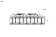
- FIG. 1 is a schematic sectional view of a wiring board according to a first embodiment of the present invention.
- FIG. 2 is a schematic cross-sectional view of a semiconductor device in which a semiconductor chip is mounted on the wiring board of FIG. 1 according to the first embodiment of the present invention.
- FIG. 3A is a schematic cross-sectional view illustrating a part of the steps for manufacturing the wiring board in FIG. 1 up to the manufacturing of the interposer with a support according to the first embodiment of the present invention.
- FIG. 3B is a schematic cross-sectional view illustrating a part of the steps for manufacturing the wiring board in FIG. 1 up to the manufacturing of the interposer with a support according to the first embodiment of the present invention.
- FIG. 1 is a schematic sectional view of a wiring board according to a first embodiment of the present invention.
- FIG. 2 is a schematic cross-sectional view of a semiconductor device in which a semiconductor chip is mounted on the wiring board of FIG. 1 according to the first embodiment of the present invention.
- FIG. 3C is a schematic cross-sectional view illustrating a part of the steps for manufacturing the wiring board in FIG. 1 up to the manufacturing of the interposer with a support according to the first embodiment of the present invention.
- FIG. 3D is a schematic cross-sectional view illustrating a part of the steps for manufacturing the wiring board in FIG. 1 up to the manufacturing of the interposer with a support according to the first embodiment of the present invention.
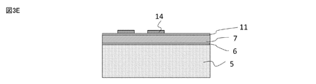
- FIG. 3E is a schematic cross-sectional view illustrating a part of the manufacturing process of the wiring board of FIG. 1 up to the manufacture of the interposer with a support according to the first embodiment of the present invention.
- FIG. 3C is a schematic cross-sectional view illustrating a part of the steps for manufacturing the wiring board in FIG. 1 up to the manufacturing of the interposer with a support according to the first embodiment of the present invention.
- FIG. 3D is a schematic cross-sectional view illustrating a part of the steps for manufacturing the wiring board in FIG. 1 up to the manufacturing
- FIG. 4A is a schematic cross-sectional view illustrating a part of the process up to manufacturing of the interposer with a support, following FIGS. 3A to 3E.
- 4B is a schematic cross-sectional view illustrating a part of the process up to the manufacturing of the interposer with a support, following FIGS. 3A to 3E.
- FIG. 4C is a schematic cross-sectional view illustrating a part of the process up to manufacturing of the interposer with a support, following FIGS. 3A to 3E.
- FIG. 4D is a schematic cross-sectional view illustrating a part of the process up to manufacturing of the interposer with a support, following FIGS. 3A to 3E.
- FIG. 4E is a schematic cross-sectional view illustrating a part of the process up to manufacturing of the interposer with a support, following FIGS. 3A to 3E.
- FIG. 5A is a schematic cross-sectional view illustrating a part of the process up to manufacturing of the interposer with a support, following FIGS. 4A to 4E.
- FIG. 5B is a schematic cross-sectional view illustrating a part of the process up to manufacturing of the interposer with a support, following FIGS. 4A to 4E.
- FIG. 5C is a schematic cross-sectional view illustrating a part of the process up to manufacturing of the interposer with a support, following FIGS. 4A to 4E.
- FIG. 5A is a schematic cross-sectional view illustrating a part of the process up to manufacturing of the interposer with a support, following FIGS. 4A to 4E.
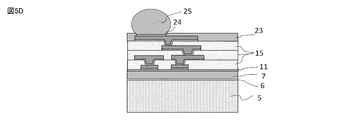
- FIG. 5D is a schematic cross-sectional view illustrating a part of the process up to manufacturing of the interposer with a support, following FIGS. 4A to 4E.
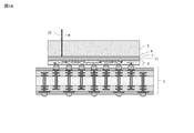
- FIG. 6A is a schematic cross-sectional view illustrating a part of the manufacturing process of the wiring board in FIG. 1 subsequent to FIGS. 5A to 5D.
- FIG. 6B is a schematic cross-sectional view illustrating a part of the manufacturing process of the wiring board in FIG. 1 subsequent to FIGS. 5A to 5D.
- FIG. 7A is a schematic cross-sectional view illustrating a part of the manufacturing process of the wiring board in FIG. 1, following FIGS. 6A and 6B. 7B is a schematic cross-sectional view illustrating a part of the manufacturing process of the wiring board in FIG.
- FIG. 8A is a schematic cross-sectional view illustrating the manufacturing process of the wiring board of FIG. 1 and the semiconductor device of FIG. 2, following FIGS. 7A to 7C.
- 8B is a schematic cross-sectional view illustrating the manufacturing process of the wiring board of FIG. 1 and the semiconductor device of FIG. 2, following FIGS. 7A to 7C.
- FIG. 8C is a schematic cross-sectional view illustrating the manufacturing process of the wiring board of FIG. 1 and the semiconductor device of FIG. 2, following FIGS. 7A to 7C.
- FIG. 9 is a schematic cross-sectional view of a wiring board which is a reference example.
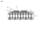
- FIG. 10 is a schematic cross-sectional view showing an example in which a semiconductor chip is mounted on the wiring board according to the second embodiment of the present invention.
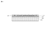
- FIG. 11 is a schematic cross-sectional view showing a state in which the second wiring board (interposer) according to the second embodiment of the present invention is provided with a support.
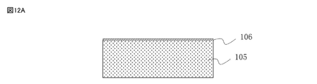
- FIG. 12A is a schematic explanatory view of an example of a manufacturing process of a second wiring board (interposer) provided with a support according to a schematic sectional view according to the second embodiment of the present invention.
- FIG. 12B is a schematic explanatory view of an example of the manufacturing process of the second wiring board (interposer) provided with the support according to the schematic sectional view according to the second embodiment of the present invention.
- FIG. 12A is a schematic explanatory view of an example of a manufacturing process of a second wiring board (interposer) provided with a support according to a schematic sectional view according to the second embodiment of the present invention.
- FIG. 12B is
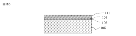
- FIG. 12C is a schematic explanatory view of an example of a manufacturing process of a second wiring board (interposer) provided with a support according to the schematic sectional view according to the second embodiment of the present invention.
- FIG. 12D is a schematic explanatory view of an example of a manufacturing process of the second wiring board (interposer) provided with the support according to the schematic sectional view according to the second embodiment of the present invention.
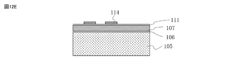
- FIG. 12E is a schematic explanatory view of an example of a manufacturing process of the second wiring board (interposer) provided with the support according to the schematic sectional view according to the second embodiment of the present invention.
- FIG. 12C is a schematic explanatory view of an example of a manufacturing process of a second wiring board (interposer) provided with a support according to the schematic sectional view according to the second embodiment of the present invention.
- FIG. 12D is a schematic explanatory view of an example of a manufacturing process of the second wiring board (interposer) provided with the support according to the schematic
- FIG. 12F is a schematic explanatory view of an example of a manufacturing process of the second wiring board (interposer) provided with the support according to the schematic sectional view according to the second embodiment of the present invention.
- FIG. 12G is a schematic explanatory view of an example of a manufacturing process of the second wiring board (interposer) provided with the support according to the schematic sectional view according to the second embodiment of the present invention.
- FIG. 12H is a schematic explanatory view of an example of a manufacturing process of the second wiring board (interposer) provided with the support according to the schematic sectional view according to the second embodiment of the present invention.
- FIG. 12F is a schematic explanatory view of an example of a manufacturing process of the second wiring board (interposer) provided with the support according to the schematic sectional view according to the second embodiment of the present invention.
- FIG. 12G is a schematic explanatory view of an example of a manufacturing process of the second wiring board (interposer) provided with the support according to the schematic sectional view according
- FIG. 12I is a schematic explanatory view of an example of a manufacturing process of the second wiring board (interposer) provided with the support according to the schematic sectional view according to the second embodiment of the present invention.
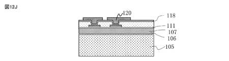
- FIG. 12J is a schematic explanatory view of an example of a manufacturing process of a second wiring board (interposer) provided with a support according to a schematic sectional view according to the second embodiment of the present invention.
- FIG. 12K is a schematic explanatory view of an example of a manufacturing process of the second wiring board (interposer) provided with the support according to the schematic sectional view according to the second embodiment of the present invention.
- FIG. 12I is a schematic explanatory view of an example of a manufacturing process of the second wiring board (interposer) provided with the support according to the schematic sectional view according to the second embodiment of the present invention.
- FIG. 12J is a schematic explanatory view of an example of a manufacturing process of a second wiring board (interposer) provided with a support according to
- FIG. 12L is a schematic explanatory view of an example of the manufacturing process of the second wiring board (interposer) provided with the support according to the schematic sectional view according to the second embodiment of the present invention.
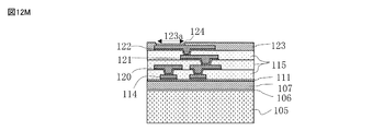
- FIG. 12M is a schematic explanatory view of an example of a manufacturing process of the second wiring board (interposer) provided with the support according to the schematic sectional view according to the second embodiment of the present invention.
- FIG. 12N is a schematic explanatory view of an example of a manufacturing process of a second wiring board (interposer) provided with a support according to the schematic sectional view according to the second embodiment of the present invention.
- FIG. 12M is a schematic explanatory view of an example of a manufacturing process of the second wiring board (interposer) provided with the support according to the schematic sectional view according to the second embodiment of the present invention.
- FIG. 12N is a schematic explanatory view of an example of a manufacturing process of a second wiring board (interposer) provided with a support according to the schematic section
- FIG. 13A is a schematic explanatory diagram of an example of a manufacturing process of a wiring board and a semiconductor device according to a schematic sectional view according to a second embodiment of the present invention.
- FIG. 13B is a schematic explanatory view of an example of a manufacturing process of a wiring board and a semiconductor device according to a schematic sectional view according to a second embodiment of the present invention.
- FIG. 13C is a schematic explanatory view of an example of a manufacturing process of a wiring board and a semiconductor device according to a schematic sectional view according to a second embodiment of the present invention.
- FIG. 13A is a schematic explanatory diagram of an example of a manufacturing process of a wiring board and a semiconductor device according to a schematic sectional view according to a second embodiment of the present invention.
- FIG. 13B is a schematic explanatory view of an example of a manufacturing process of a wiring board and a semiconductor device according to a schematic sectional view according to a second embodiment of the present invention.
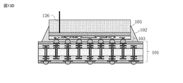
- FIG. 13D is a schematic explanatory view of an example of a manufacturing process of a wiring board and a semiconductor device according to a schematic sectional view according to a second embodiment of the present invention.
- FIG. 13E is a schematic explanatory view of an example of a manufacturing process of a wiring board and a semiconductor device according to a schematic sectional view according to a second embodiment of the present invention.
- FIG. 13F is a schematic explanatory view of an example of a manufacturing process of a wiring board and a semiconductor device according to a schematic sectional view according to a second embodiment of the present invention.
- FIG. 13D is a schematic explanatory view of an example of a manufacturing process of a wiring board and a semiconductor device according to a schematic sectional view according to a second embodiment of the present invention.
- FIG. 13E is a schematic explanatory view of an example of a manufacturing process of a wiring board and a semiconductor device according to a schematic sectional view according to a second embodiment of the present invention.
- FIG. 13G is a schematic explanatory view of an example of a manufacturing process of a wiring board and a semiconductor device according to a schematic sectional view according to a second embodiment of the present invention.
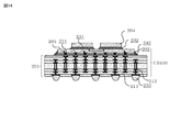
- FIG. 14 is a sectional view showing an example of a semiconductor package in which a semiconductor chip is mounted on a wiring board according to the third embodiment of the present invention.
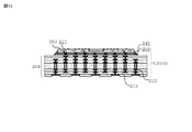
- FIG. 15 is a sectional view showing an example of a wiring board according to the third embodiment of the present invention.
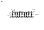
- FIG. 16 is a sectional view showing an example of a wiring board according to the third embodiment of the present invention.
- FIG. 17 is a sectional view showing an example of a wiring board according to the third embodiment of the present invention.
- FIG. 14 is a sectional view showing an example of a semiconductor package in which a semiconductor chip is mounted on a wiring board according to the third embodiment of the present invention.
- FIG. 15 is a sectional view showing an example of a wiring board according to the third embodiment of the present invention.
- FIG. 16
- FIG. 18A is a sectional view showing an example of a manufacturing process of the wiring board according to the third embodiment of the present invention.
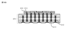
- FIG. 18B is a sectional view showing an example of a manufacturing process of the wiring board according to the third embodiment of the present invention.
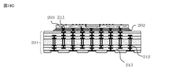
- FIG. 18C is a sectional view showing an example of a manufacturing process of the wiring board according to the third embodiment of the present invention.
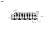
- FIG. 18D is a sectional view showing an example of a manufacturing process of the wiring board according to the third embodiment of the present invention.
- FIG. 18E is a sectional view showing an example of a manufacturing process of the wiring board according to the third embodiment of the present invention.
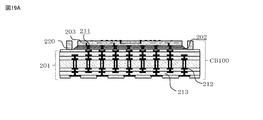
- FIG. 19A is a sectional view showing an example of a manufacturing process of the wiring board according to the third embodiment of the present invention.
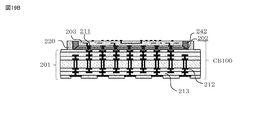
- FIG. 19B is a sectional view showing an example of a manufacturing process of the wiring board according to the third embodiment of the present invention.
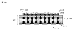
- FIG. 19C is a sectional view showing an example of a
- a semiconductor device wiring board (hereinafter, simply referred to as a wiring board) according to an embodiment of the present invention will be described below with reference to the drawings.
- a wiring board A semiconductor device wiring board (hereinafter, simply referred to as a wiring board) according to an embodiment of the present invention will be described below with reference to the drawings.
- portions corresponding to each other are designated by the same reference numerals, and overlapping portions will not be described below as appropriate. Further, each drawing is exaggerated as appropriate for ease of explanation.
- the embodiment of the present invention exemplifies a configuration for embodying the technical idea of the present invention, and the material, shape, structure, arrangement, etc. of each part are not specified below.
- the technical idea of the invention can be modified within the technical scope defined by the claims described in the claims.
- FIG. 1 is a schematic cross-sectional view of a wiring board according to an embodiment of the present invention.
- the wiring board CB100 includes an FC-BGA wiring board (first wiring board) 1 and an interposer (second wiring board) 3.
- the FC-BGA wiring board 1 and the interposer 3 are electrically bonded to each other via the solder bumps 25 as the protruding electrodes, and the underfill 2 as a sealing resin is provided in the gap between the FC-BGA wiring board 1 and the interposer 3. It is filled.
- the bump electrode may be a copper post (copper pillar), a gold bump, or the like, other than the solder bump.
- the underfill 2 is an adhesive material used to fix and seal the FC-BGA wiring board 1 and the interposer 3.
- the underfill 2 for example, one kind of epoxy resin, urethane resin, silicone resin, polyester resin, oxetane resin, and maleimide resin, or a resin in which two or more kinds of these resins are mixed, and silica as a filler are used.
- a material added with titanium oxide, aluminum oxide, magnesium oxide, zinc oxide, or the like is used.
- the underfill 2 is formed by filling a liquid resin and curing it.
- the underfill 2 is not only the gap between the interposer 3 and the FC-BGA wiring board 1, but also the entire side surface of the interposer 3 and the surface where the interposer 3 is joined to the FC-BGA wiring board 1. The edge of the opposite surface (upper surface in FIG. 1) is covered.
- the underfill 2 is applied and formed only in the gap between the interposer 3 and the FC-BGA wiring board 1, since the interposer 3 is made of an organic resin, thermal stress concentrates in the plane center direction of the gap, -Deformation and displacement stress occur between the BGA wiring board 1 and the BGA wiring board 1.
- the underfill 2 is applied to the entire side surface of the interposer 3 and the peripheral edge portion of the surface opposite to the surface where the interposer 3 is joined to the FC-BGA wiring board 1. Since it is hardened, thermal stress is dispersed in multiple directions, and the effect of relaxing the concentration of stress is exhibited. Thus, the interposer 3 and the FC-BGA wiring board 1 can exhibit high connection reliability.
- FIG. 2 is a schematic cross-sectional view of a semiconductor device in which a semiconductor chip is mounted on the wiring board of FIG. 1 according to the first embodiment of the present invention.
- the semiconductor chip 4 is bonded to the semiconductor chip 4 via the copper pillar 30 on the surface of the interposer 3 of the wiring board CB100 of FIG. 1 opposite to the FC-BGA wiring board 1.
- a gap between the interposer 3 and the interposer 3 is filled with an underfill 32.
- the underfill 32 is an adhesive used to fix and seal the semiconductor chip 4 and the interposer 3, and is made of the same material as the underfill 2.
- an anisotropic conductive film (ACF) or a film-like connecting material (NCF) may be used as a sealing resin instead of the underfill 32.
- the wiring pitch of the portion of the interposer 3 to be joined to the semiconductor chip 4 is the portion to be joined to the semiconductor chip 4 of the FC-BGA wiring board 1 when the semiconductor chip 4 and the FC-BGA wiring board 1 are directly joined. Narrower than the wiring pitch. That is, the surface of the interposer 3 on which the semiconductor chip 4 is mounted has finer wiring than that of the FC-BGA wiring board 1 when the semiconductor chip 4 is joined.
- the interposer 3 in order to support the current use of high-band memory (HBM), the interposer 3 needs to have a wiring width of 2 ⁇ m or more and 6 ⁇ m or less.
- the insulating film thickness between the wirings is 2.5 ⁇ m.
- the thickness of one layer including wiring is 4.5 ⁇ m, and when forming five layers of interposer 3 with this thickness, the interposer 3 becomes an extremely thin interposer with a total thickness of about 25 ⁇ m.
- the interposer 3 is thin and it is difficult to mount it on the FC-BGA wiring board 1 as it is, the interposer 3 is required to have rigidity. Further, a flat support is required to form a wiring having a width and a height of about 2 ⁇ m. For this reason, as will be described later, the interposer 3 is formed on a rigid and flat support through the release layer, the protective layer, and the seed layer. A layer other than the peeling layer, the protective layer and the seed layer may be provided on the support.
- a release layer 6 for removing the support 5 in a later step is formed on one surface of the support 5.
- the peeling layer 6 may be a resin that can be peeled by UV light or infrared light, or may be a resin that foams by heat.
- the support 5 is irradiated with UV light or infrared light from the surface opposite to the side where the peeling layer 6 is provided, and the interposer 3 and The support 5 is removed from the bonded body with the FC-BGA wiring board 1. Therefore, the support 5 needs to have transparency, and for example, glass can be used.
- the glass has excellent flatness and is suitable for forming a fine wiring pattern of the interposer 3. Further, since the glass has a small coefficient of thermal expansion and is hard to be distorted, the pattern arrangement accuracy when bonded to the FC-BGA wiring board 1 is high. And excellent in securing flatness.
- the thickness of the glass is preferably thick from the viewpoint of suppressing warpage in the manufacturing process, for example, 0.7 mm or more and 1.1 mm or less.
- the coefficient of thermal expansion of glass is 3 ppm/° C. or more and 15 ppm/° C. or less, and is preferably about 9 ppm/° C. from the viewpoint of the thermal expansion coefficient of the FC-BGA wiring board and semiconductor chip.
- glass is used as the support 5.
- the support 5 can be removed by heating the bonded body of the interposer 3 and the FC-BGA wiring board 1.
- the support 5 can be made of metal or ceramics with less distortion.
- the protective layer 7 is a layer for protecting the interposer 3 when the support 5 is peeled off in a later step, and is one of epoxy resin, acrylic resin, urethane resin, silicon resin, polyester resin, oxetane resin, or one of these. It is a resin in which two or more kinds of resins are mixed, and is a resin that can be removed after the support 5 is removed from the interposer 3.
- the protective layer 7 may be formed by spin coating, laminating, or the like depending on the shape of the resin. In one embodiment of the present invention, an acrylic resin is formed by a laminating method to form the protective layer 7.
- a seed layer 11 is formed on the protective layer 7 by a sputtering method or the like in vacuum.
- titanium layer/copper layer (Ti/Cu), chrome layer/copper layer (Cr/Cu), nickel chrome layer/copper layer (NiCr/Cu), etc. are appropriately layered according to the application. , The thickness can be selected.
- the seed layer 11 is formed with Ti: 50 nm thick and Cu: 300 nm thick.
- a resist pattern 13 is formed on the seed layer, and a conductor layer 14 serving as a wiring pattern is formed in the opening 13a by electrolytic plating.
- copper Cu is formed as the conductor layer 14.
- a photosensitive insulating resin layer 15 is formed on the seed layer 11 and the conductor layer 14.
- the photosensitive insulating resin layer 15 is formed so that the conductor layer 14 is embedded in the layer of the photosensitive insulating resin layer 15.
- an epoxy resin is used as the photosensitive insulating resin by spin coating.
- the photosensitive epoxy resin can be cured at a relatively low temperature, has little shrinkage due to curing (curing) after formation of the conductive via, and is also excellent in subsequent fine pattern formation.
- the photosensitive insulating resin layer 15 can be formed by spin coating using a photosensitive epoxy resin, or by forming an insulating resin film by compression curing with a vacuum laminator. In this case, An insulating film having good flatness can be formed. Polyimide may be used as the photosensitive insulating resin as long as a slight level difference can be allowed in the exposure step.
- the photosensitive insulating resin layer 15 may be a positive type or a negative type.
- an opening 15a is provided on the conductor layer 14 of the photosensitive insulating resin layer 15 by photolithography.
- the opening 15a may be subjected to plasma treatment for the purpose of removing residues after development.
- a seed layer 18 is provided on the surface of the opening 15a.
- a layer configuration and a thickness such as Ti/Cu, Cr/Cu, and NiCr/Cu can be appropriately selected according to the application.
- the seed layer 18 is formed with Ti: 50 nm thick and Cu: 300 nm thick.
- a resist pattern 19 is formed on the seed layer 18, and a conductor layer 20 to be a wiring pattern is formed in the opening 19a by electrolytic plating.
- copper Cu is formed as the conductor layer 20.
- the unnecessary seed layer 18 is removed by etching.
- FIGS. 4A to 4E are repeated to obtain the substrate having the multilayer wiring pattern shown in FIG. 5A.
- the insulating resin layer 23 is formed on the outermost surface of the interposer on the side to be joined to the FC-BGA wiring board 1.
- the insulating resin layer 23 is formed so as to cover the conductor layer 22 and the photosensitive insulating resin layer 15, and an opening 23a is formed in the insulating resin layer 23 so that the conductor layer 22 is exposed by exposure and development.
- the insulating resin layer 23 is formed by using a photosensitive epoxy resin as the insulating resin.
- the insulating resin may be the same material as the photosensitive insulating resin layer 15.
- a surface treatment layer 24 is provided in order to prevent oxidation of the surface of the conductor layer 22 and improve wettability of the solder bumps.
- electroless nickel-lead-gold (Ni/Pd/Au) plating is formed as the surface treatment layer 24.
- the surface treatment layer 24 may be formed with an OSP (Organic Soilerability Preservative, surface treatment with water-soluble preflux) film.
- OSP Organic Soilerability Preservative, surface treatment with water-soluble preflux
- electroless tin plating, electroless nickel gold (Ni/Au) plating, etc. may be appropriately selected and used according to the application.
- solder bumps 25 are mounted on the surface treatment layer 24 and reflowed to complete the interposer with the support 5.
- reflow solder can be bonded to parts by printing cream solder etc. in a designated place in advance and heating it in a reflow oven to melt it, as opposed to flow solder that applies melted solder from the beginning. Is.
- FIGS. 6A to 8C a manufacturing process of the wiring board CB100 and the semiconductor device SD100 of FIG. 1 following FIG. 5D will be exemplified.
- the FC-BGA wiring board 1 designed and manufactured so as to match the positions of the solder bumps 25 which are the terminals of the interposer 3 with the support 5 is provided with the interposer 3 with the support 5 by flip chip. Deploy.
- FIG. 6B a joined body is obtained in which the interposer 3 with the support body 5 and the FC-BGA wiring board 1 are joined via the solder bumps 25.
- laser light 26 is transmitted from the back surface of the support body 5, that is, the surface of the support body 5 opposite to the FC-BGA wiring substrate 1 side, to the interface through the support body 5.
- the formed peeling layer 6 is irradiated, and the support 5 is peeled and removed as shown in FIG. 7B.
- the interposer 3 and the FC-BGA wiring board 1 are joined by the solder bumps 25, they are not separated when the support body 5 is removed.
- the peeling layer 6, the protective layer 7, and the seed layer 11 are removed to obtain a substrate as shown in FIG. 8A.
- the peeling layer 6 is mechanically peeled off from the protective layer 7.
- the protective layer 7 is removed with an alkaline solvent (1% NaOH, 2.3% TMAH).
- the seed layer 11 is dissolved and removed with an alkaline etching agent and an acid etching agent, respectively.
- underfill 2 is applied to the gap between the interposer 3 and the FC-BGA wiring board 1, and the entire side surface of the interposer 3 and the surface of the interposer 3 to be joined to the FC-BGA wiring board 1.
- the underfill 2 is also applied to the peripheral edge portion of the opposite surface and heat cured.
- the underfill 2 is first filled in the gap between the interposer 3 and the FC-BGA wiring board 1 using a capillary (not shown).
- the side surface and the peripheral edge portion of the interposer 3 are directly formed by scanning the coating head (not shown) of the jet dispenser. In this way, the wiring board CB100 is obtained.
- a surface treatment layer such as electroless Ni/Pd/Au plating, OSP, electroless tin plating, or electroless Ni/Au plating is formed on the conductor layer 14 exposed on the surface in the same manner as in the step of FIG. 5C. (Not shown) may be formed.
- the semiconductor chip 4 is joined to the wiring board CB100 by a known method, and as shown in FIG. 8C, the gap between the wiring board CB100 and the semiconductor chip 4 is filled with the underfill 32 to manufacture the semiconductor device SD100. can do.
- FIG. 9 is a schematic cross-sectional view of a wiring board CB200 which is a reference example.
- an interposer 3 including a fine wiring layer in which a resin and wiring are laminated is produced on a flat support as in this embodiment, and the interposer 3 including the support is manufactured.
- an underfill 42 as a sealing resin is filled in the gap between the interposer 3 and the FC-BGA wiring board 1.
- the wiring board CB200 in which the interposer 3 is bonded onto the FC-BGA wiring board 1 is manufactured.
- the underfill 42 is filled in the gap between the interposer 3 and the FC-BGA wiring board 1, it is necessary to select a material that does not easily damage the solder, and the degree of freedom in material selection is limited.
- the underfill 42 may travel up (wet up) along the side surface of the interposer 3 due to surface tension, and may reach the middle of the interposer 3 in the thickness direction. In this case, the underfill 42 becomes thinner as it goes upward, and the underfill 42 is discontinued at the boundary point BD.
- the wiring board manufactured by the manufacturing method according to the present embodiment in the bonded body of the interposer and the FC-BGA wiring board formed on the support, after the interposer and the FC-BGA wiring board are bonded, The support is peeled off, and then an underfill is applied to the gap between the FC-BGA wiring board and the interposer, the entire side surface of the interposer, and the peripheral edge of the surface opposite to the surface where the interposer is joined to the FC-BGA wiring board. Since it is formed by filling and covering, concentration of stress due to curing of the underfill is relieved, disconnection of the joint between the interposer and the FC-BGA wiring board can be prevented, and thus connection reliability of the joint can be improved. it can.
- FIG. 10 is a schematic cross-sectional view of a semiconductor device in which a semiconductor chip is mounted on the wiring board according to the second embodiment.
- the wiring board according to the present embodiment includes an FC-BGA wiring board 101 as a first wiring board, and a fine wiring layer formed only by a build-up wiring layer in which a resin and wiring are laminated as a second wiring board.
- the thin interposer 103 is used. More specifically, the wiring board includes a second wiring board (interposer) 103 joined to the main surface of the first wiring board (FC-BGA wiring board) 101.
- the first wiring board (FC-BGA wiring board) 101 and the second wiring board (interposer) 103 are electrically joined to each other via the protruding electrode 125, and the first wiring board (FC-BGA wiring board) 101 and the second wiring board
- the gap of the wiring board (interposer) 103 is filled with an insulating sealing resin 102.
- the sealing resin 102 is continuous outside the gap between the first wiring board (FC-BGA wiring board) 101 and the second wiring board (interposer) 103 and covers the entire side surface of the second wiring board (interposer) 103.
- a bank peripheral wall that is an upper surface having a height that exceeds the upper surface of the second wiring board is formed.
- the second wiring board (interposer) 103 has pads 140 (FIG. 13F) on the surface opposite to the first wiring board (FC-BGA wiring board) 101 side.
- the protruding electrode 125 (see FIG. 13A) is composed of a solder bump, a copper post (copper pillar), or a gold bump. Further, a semiconductor chip 104 is joined to a surface of the second wiring board (interposer) 103 opposite to the first wiring board (FC-BGA wiring board) 101 by a copper pillar 131, and the semiconductor chip 104 and the second wiring board ( The gap with the interposer) 103 is filled with the sealing resin 132, and the height of the sealing resin 132 is formed higher than that of the second wiring board (interposer) 103.
- the sealing resin 102 is an adhesive material used to fix and seal the first wiring board (FC-BGA wiring board) 101 and the second wiring board (interposer) 103.
- the sealing resin 102 include epoxy resin, urethane resin, silicon resin, polyester resin, oxetane resin, and maleimide resin, or a resin in which two or more kinds of these resins are mixed, silica as a filler, A material to which titanium oxide, aluminum oxide, magnesium oxide, zinc oxide, or the like is added is used.
- the sealing resin 102 is formed by filling a liquid resin.
- the sealing resin 132 is an adhesive used to fix and seal the semiconductor chip 104 and the interposer 103, and is made of the same material as the sealing resin 102.
- an anisotropic conductive film (ACF:anisotropic conductive film) or a film-like connecting material (NCF:non conductive film) may be used as the sealing resin 132.
- the wiring pitch of the portion of the second wiring substrate (interposer) 103 that is joined to the semiconductor chip 104 is the same as the wiring pitch of the portion that is joined to the semiconductor chip 104.
- the semiconductor chip 104 and the FC-BGA wiring substrate 101 are directly joined.
- the wiring pitch is narrower than the wiring pitch of the portion of the first wiring board (FC-BGA wiring board) 101 to be joined to the semiconductor chip 104. That is, the surface of the second wiring board (interposer) 103 on which the semiconductor chip 104 is mounted has finer wiring than that of the FC-BGA wiring board 101 when bonded to the semiconductor chip 104.
- the wiring width of the second wiring board (interposer) 103 needs to be 2 ⁇ m or more and 6 ⁇ m or less.
- the insulating film thickness between the wirings is 2.5 ⁇ m.
- the thickness of one layer including wiring is 4.5 ⁇ m.
- the total thickness of the second wiring substrate (interposer) 103 is about 25 ⁇ m. It becomes an ultra-thin interposer.
- the second wiring board (interposer) 103 since the thickness of the second wiring board (interposer) 103 is thin and it is difficult to mount it on the FC-BGA wiring board 101 as it is, the second wiring board (interposer) 103 has no rigidity. Desired. Further, a flat support is required to form a wiring having a width and a height of about 2 ⁇ m. For the above reason, as shown in FIG. 11, the second wiring substrate (interposer) 103 is formed on the rigid and flat support 105 with the peeling layer 106, the protective layer 107, and the seed layer 108 interposed therebetween. A layer other than the peeling layer, the protective layer and the seed layer may be provided on the support.
- a wiring board to be the second wiring board (interposer) 103 is formed on the support 105.
- a release layer 106 for releasing the support 105 is formed on one surface of the support 105 in a later step (release layer forming step).
- the protective layer 107 is a layer for protecting the second wiring substrate (interposer) 103 when the support 105 is peeled off in a later step, and is made of epoxy resin, acrylic resin, urethane resin, silicon resin, polyester resin, oxetane resin. 1 or a mixture of two or more of these resins, and is a resin that can be removed after the second wiring substrate (interposer) 103 is peeled from the support 105.
- the protective layer 107 may be appropriately formed by spin coating, laminating, or the like depending on the shape of the resin. For example, an acrylic resin is formed by a laminating method.
- the peeling layer 106 may be a resin that can be peeled by UV light or infrared light, or a resin that is foamed by heat.
- the support 105 is irradiated with UV light or infrared light from the surface opposite to the side where the peeling layer 106 is provided, and the second wiring substrate The support 105 is peeled off and removed from the bonded body of the (interposer) 103 and the first wiring board (FC-BGA wiring board) 101.
- the support 105 needs to have transparency, and glass can be used, for example.
- the thickness of the glass is preferably thick from the viewpoint of suppressing the occurrence of warpage in the manufacturing process.
- the thickness is preferably 0.7 mm or more and 1.1 mm or less.
- the coefficient of linear expansion (CTE: Coefficient of Thermal Expansion) of glass is 3 ppm/° C. or more and 15 ppm/° C. or less, and 9 ppm from the viewpoint of the coefficient of linear expansion (CTE: Coefficient of Thermal Expansion) of the FC-BGA wiring substrate and the semiconductor chip. /°C is desirable.
- glass is used as the support 105.
- the support is obtained by heating the bonded body of the second wiring board (interposer) 103 and the first wiring board (FC-BGA wiring board) 101. Remove 105.
- the support 105 can be made of metal or ceramics with less distortion.
- a seed layer 111 is formed on the protective layer 107 in vacuum.
- titanium (Ti)/copper (Cu), chrome (Cr)/copper (Cu), chrome nickel (NiCr)/copper (Cu), etc. the structure and thickness of which can be appropriately changed depending on the application.
- the seed layer 111 can be formed of titanium (Ti): 50 nm and copper (Cu): 300 nm.
- a resist pattern 113 is formed on the seed layer 111, and a conductor layer 114 is formed in the opening 113a by electrolytic plating.
- a conductor layer 114 is formed in the opening 113a by electrolytic plating.
- Cu is formed as the conductor layer 114.
- the resist pattern 113 is removed as shown in FIG. 12E.
- a photosensitive insulating resin layer 115 is formed on the conductor layer 114 and the seed layer 111.
- the photosensitive insulating resin layer 115 is formed so that the conductor layer 114 is embedded in the layer of the photosensitive insulating resin layer 115.
- it can be formed by a spin coating method using an epoxy resin as the photosensitive insulating resin.
- the photosensitive epoxy resin can be cured at a relatively low temperature, has little shrinkage due to curing (curing) after the formation of the conductive via, and is excellent in the subsequent fine pattern formation.
- the photosensitive insulating resin layer 115 can be formed by spin coating using a photosensitive epoxy resin, or can be formed by compressing and curing an insulating resin film with a vacuum laminator. An insulating film having good properties can be formed. Polyimide may be used as the insulating resin as long as a slight level difference can be allowed in the exposure step.
- an opening 115a is provided on the conductor layer 114 by photolithography.
- the opening 115a may be subjected to plasma treatment for the purpose of removing a residue during development.
- a seed layer 118 is provided on the surface of the opening 115a.
- titanium (Ti)/copper (Cu), chrome (Cr)/copper (Cu), chrome nickel (NiCr)/copper (Cu), etc. the structure and thickness of which can be appropriately changed depending on the application. is there.
- the seed layer 118 can be formed of titanium (Ti): 50 nm and copper (Cu): 300 nm.
- a resist pattern 119 is formed on the seed layer 118, and a conductor layer 120 is formed in the opening 119a by electrolytic plating.
- a conductor layer 120 is formed in the opening 119a by electrolytic plating.
- copper (Cu) is formed as the conductor layer 120.
- the resist pattern 119 is removed, and the unnecessary seed layer 118 is removed by etching.
- FIGS. 12F to 12J are repeated to obtain a substrate having the multilayer wiring pattern shown in FIG. 12K.
- wiring layer forming step it is possible to form a wiring layer in which the surface on the release layer 106 side becomes the first pad and the side opposite to the release layer 106 becomes the second pad (wiring layer forming step).
- the photosensitive insulating resin layer 115 may be a positive type or a negative type.
- an insulating resin layer 123 is formed on the outermost surface of the second wiring board (interposer) 103 on the first wiring board (FC-BGA wiring board) 101 side.
- the insulating resin layer 123 is formed so as to cover the conductor layer 122 and the photosensitive insulating resin layer 115, and an opening 123a is formed in the insulating resin layer 123 so that the conductor layer 122 is exposed by exposure and development.
- the insulating resin layer 123 is formed using a photosensitive epoxy resin as the insulating resin.
- the insulating resin may be the same material as the photosensitive insulating resin layer 115.
- a surface treatment layer 124 is provided in order to prevent oxidation of the surface of the conductor layer 122 and improve wettability of the solder bumps.
- electroless nickel (Ni)/palladium (Pd)/gold (Au) plating is formed as the surface treatment layer 124.
- the surface treatment layer 124 may be formed with an OSP (Organic Soderability Preservative, surface treatment with water-soluble preflux) film.
- electroless tin plating, electroless nickel (Ni)/gold (Au) plating, etc. may be appropriately selected and used according to the application.
- solder bumps are mounted on the surface treatment layer 124 as the projection electrodes 125 and reflowed to form the projection electrodes on the surface of the second pad (projection electrode forming step).
- the second wiring board (interposer) 105 is completed.
- An example of a series of manufacturing steps up to the step of filling and injecting the resin 102, the step of peeling the support 105, the step of exposing the wiring board pad, and the step of mounting the semiconductor chip will be described.
- the protruding electrodes 125 of the second wiring board (interposer) 103 with the support 105 and the first wiring board pads of the first wiring board (FC-BGA wiring board) 101 are electrically connected. Joining (electrical joining process).
- the sealing resin 102 is injected into the gap between the first wiring board (FC-BGA wiring board) 101 and the second wiring board (interposer) 103 to protect the solder joints ( Sealing resin filling and injecting step).
- An appropriate injection amount may be set for the sealing resin 102 depending on the volume of the gap between the first wiring board (FC-BGA wiring board) 101 and the second wiring board (interposer) 103.
- the height of the sealing resin 102 be set to be 1.2 times or more the volume of the gap between the first wiring board (FC-BGA wiring board) 101 and the second wiring board (interposer) 103. It can be formed higher than the two-wiring board (interposer) 103.
- the sealing resin 102 is transferred to the side surface of the support 105 through the side surface of the second wiring substrate (interposer) 103, the seed layer 111, the protective layer 107, and the side surface of the peeling layer 106 due to wetting.
- the upper end of the sealing resin 102 is shown to be sharp in the drawing, it may actually be rounded to some extent.
- the support 105 may be subjected to an underfill repellent treatment.
- the underfill repellent treatment include fluorine coating and silicone coating treatment, which may be appropriately set depending on the application.
- the laser light 126 and the support body 105 are removed.
- the peeling layer 106 formed on the interface after being transmitted is irradiated, and the support 105 is peeled and removed together with the peeling layer 106 as shown in FIG. 13E (support peeling step).
- the sealing resin filling/injecting step may not be performed before the support peeling step, and the sealing resin filling/injecting step may be performed after the support peeling step.
- the peeling layer 106, the protective layer 107, and the seed layer 111 are removed, that is, the pads 140 of the wiring board are exposed (pad exposing step), and a wiring board as shown in FIG. 13F is obtained.
- the release layer 106 can be mechanically torn off from the protective layer 107.
- an acrylic resin is used as the protective layer 107, it is removed with an alkaline solvent (1% sodium hydroxide (NaOH), 2.3% tetramethylammonium hydroxide (TMAH).
- the seed layer 111 is used. Titanium (Ti) and copper (Cu) are used from the side of the protective layer 107.
- the wiring board CB100 is obtained by dissolving and removing with an alkaline etching agent and an acid etching agent, respectively.
- electroless nickel (Ni)/palladium (Pd)/gold (Au) plating OSP (Organic Soliderity Preservative, surface treatment with water-soluble pre-flux) on the conductor layer exposed on the surface as described above, Surface treatment such as electroless tin (Sn) plating and electroless nickel (Ni)/gold (Au) plating may be performed.
- the semiconductor device SD100 can be manufactured. ..
- the sealing resin 102 does not come into contact with the surface of the second wiring board 103 on the side opposite to the surface to be joined with the first wiring board 101.
- the embodiment of the present invention exemplifies a configuration for embodying the technical idea of the present invention, and specifies the material, shape, structure, arrangement, dimensions, etc. of each part as follows. Not. The technical idea of the present invention can be modified in various ways within the technical scope defined by the claims described in the claims.
- FIG. 14 is a sectional view showing an example of a semiconductor package in which a semiconductor chip is mounted on the wiring board according to the present embodiment.
- FIG. 15 is a cross-sectional view showing a wiring board before mounting a semiconductor chip.
- a thin interposer 203 having a fine wiring layer formed only of a build-up wiring layer in which a resin and wiring are laminated is provided on one surface of the FC-BGA wiring substrate 201.
- the electrodes 211 are electrically connected by solder bumps, copper (Cu) posts (Cu pillars), or gold bumps.
- the gap between the FC-BGA wiring board 201 and the interposer 203 is filled with a sealing resin (first sealing resin) 202 as an insulating adhesive member, and the sealing resin (covering the sealing resin 202 is further covered).
- the second sealing resin) 242 is filled and solidified.
- the sealing resin 242 preferably covers at least the boundary between the interposer 203 and the sealing resin 202.
- the semiconductor chip 204 is joined to the surface of the interposer 203 on the opposite side of the FC-BGA wiring substrate 201 with an electrode 231 composed of a solder bump, a Cu pillar, or a gold bump, and the gap between the semiconductor chip 204 and the interposer 203 is sealed. It is filled with a stop resin 232.
- the sealing resins 202 and 242 are adhesives used to fix and seal the FC-BGA wiring board 201 and the interposer 203.
- the sealing resins 202 and 242 for example, one of epoxy resin, polyurethane resin, silicone resin, polyester resin, oxetane resin, and maleimide resin, or a resin in which two or more kinds of these resins are mixed, and silica as a filler are used.
- a material to which titanium oxide, titanium oxide, aluminum oxide, magnesium oxide, zinc oxide, or the like is added is used.
- the sealing resins 202 and 242 may be formed by filling a liquid resin. Also, an anisotropic conductive film (ACF: Anisotropic Conductive Film) is sealed as an insulating adhesive member, or a non-conductive film (NCF: Non Conductive Film), which is a film-like connecting material having both the function of adhesion and insulation, is sealed.
- ACF Anisotropic Conductive Film
- NCF Non Conductive Film
- the sealing resin 232 is an adhesive used to fix and seal the semiconductor chip 204 and the interposer 203, and is made of the same material as the sealing resins 202 and 242. Also in this case, instead of the sealing resin 232, an anisotropic conductive film (ACF) or a non-conductive film (NCF) which is a film-shaped connecting material may be used.
- ACF anisotropic conductive film
- NCF non-conductive film
- the wiring pitch (wiring width and inter-wiring distance) of the portion of the interposer 203 that is joined to the semiconductor chip 204 is the semiconductor of the FC-BGA wiring board 201 when the semiconductor chip 204 and the FC-BGA wiring board 201 are directly connected. It is narrower than the wiring pitch (wiring width and inter-wiring distance) of the portion connected to the chip 204. That is, the surface of the interposer 203 on the side where the semiconductor chip 204 is mounted has finer wiring than that of the FC-BGA wiring board 201 in the case of joining with the semiconductor chip 204.
- the wiring width of the interposer 203 needs to be set to 2 ⁇ m or more and 6 ⁇ m or less.
- the insulating film thickness between the wirings is 2.5 ⁇ m.
- the thickness of one layer including wiring is 4.5 ⁇ m, and when a five-layer interposer is formed with this thickness, the interposer 203 becomes an extremely thin interposer with a total thickness of about 25 ⁇ m.
- the FC-BGA wiring board 201 is rigid, and if there is a CTE (Coeffient of Thermal Expansion) difference with the interposer 203, the joint is easily broken. Therefore, the gap between the FC-BGA wiring board 201 and the interposer 203 is filled with the sealing resin 202 to protect the joint.
- the side surface of the interposer 203 is filled with the sealing resin 202 and forms a portion called a fillet.
- the sealing resin 242 so as to cover the sealing resin 202, stress concentrated on the end portion of the fillet can be relieved, and high reliability can be obtained.
- the sealing resin 242 one in which either or both of elastic modulus and CTE (coefficient of thermal expansion) are between the sealing resin 202 and the interposer 203 is used.
- solder is previously formed on the interposer 203 and the connection electrodes of the FC-BGA wiring board 201.
- the solder material an alloy composed of 96.5 wt% Sn, 3.0 wt% Ag, and 0.5 wt% Cu is used.
- the material of the solder is not limited to this, and for example, a binary or ternary solder alloy containing silver, copper, indium, antimony, or the like can be used.
- solder particles it is not limited to solder particles, and other metal particles may be used.
- the particle shape is not limited to the spherical shape, and particles having other shapes such as granular shape, flaky shape and angular shape may be used.
- Flux (not shown) is applied to the area on the FC-BGA wiring board 201 where the electrode terminals 224 connected to the interposer 203 are arranged.
- the flux agent for example, one having at least one acid selected from the group consisting of (meth)acrylic acid, maleic acid, oxalic acid, malonic acid, citric acid, trimellitic acid, and tetramellitic acid, and a chelating agent Can be used.
- the interposer 203 is supported by a head (not shown) so that the electrode terminals 234 and the electrode terminals 224 arranged on the surface of the interposer 203 corresponding to the surface of the FC-BGA wiring board 201 correspond to each other. Align. Then, the interposer 203 is lowered until it hits the FC-BGA wiring board 201. This completes the placement of the interposer 203. Further, heating is performed at a temperature higher than the melting point of the solder, and the solder is melt-bonded to form the electrode 211, and the electrical connection between the FC-BGA wiring board 201 and the interposer 203 is completed, and the form shown in FIG. 18B is obtained. Become.
- reference numeral 212 indicates wiring and reference numeral 213 indicates an insulating layer.
- the flux between the FC-BGA wiring board 201 and the interposer 203 is removed by cleaning.
- the flux does not always need to be removed because it has a low residue type, but it is desirable to remove it because it causes voids in the sealing resin described later and reduces reliability.
- a gap is formed between the FC-BGA wiring board 201 and the interposer 203 based on the height of the electrode 211.
- An uncured thermosetting resin composition (liquid resin) to be the sealing resin 202 is injected into the gap between the FC-BGA wiring board 201 and the interposer 203, and is cured by curing.
- the sealing resin 202 made of a thermosetting thermosetting resin is formed (first sealing resin sealing step, see FIG. 18C).
- the interposer 203 is fixed to the FC-BGA wiring board 201 while the electrode 211 is protected by the sealing resin 202.
- the first encapsulation resin encapsulation step is a step of dropping the encapsulation resin 202 on the main surface of the FC-BGA wiring board 201, and mounting the interposer 203 on the FC-BGA wiring board 201 and at the same time as the FC-BGA board 201. And a step of filling the gaps between the interposers 203.
- the first encapsulation resin encapsulation step is a step of installing an insulating film-like resin on the main surface of the FC-BGA wiring board 201, and mounting the interposer 203 on the FC-BGA wiring board 201 at the same time.
- the step of filling the gap between the FC-BGA wiring board 201 and the interposer 203 may be included.
- thermosetting resin composition liquid resin
- sealing resin 242 made of a thermosetting thermosetting resin is formed (second sealing resin sealing step).
- the semiconductor chip 204 is mounted via electrode terminals (not shown) on the interposer 203 side of the wiring board CB100 and electrode terminals (not shown) formed on the side of the semiconductor chip 204 facing the wiring board CB100,
- the electrodes 231 are formed by applying heat above the melting temperature of the solder and melting and joining, and the electrical connection between the wiring board CB100 and the semiconductor chip 204 is completed.
- a gap is formed between the semiconductor chip 204 and the interposer 203 based on the height of the electrode 231.
- an uncured thermosetting resin composition liquid resin
- a sealing resin 232 made of a thermosetting thermosetting resin is formed (see FIG. 18E).
- the electrode terminal 233 is formed by the solder paste, but the present invention is not limited to this.
- the electrode terminal 233 may be formed by a solder ball by a melt forming method, or may be formed of Cu, Al, or gold.
- a metal pin formed of a single metal or a composite material can be used.
- the sealing resin 202 is formed in the gap between the FC-BGA wiring board 201 and the interposer 203 and a part of the side surface of the interposer 203.
- the sealing resin 242 is formed over the side surface portion of the interposer 203 so as to cover the sealing resin 202, so that the stress applied to the end portion of the sealing resin 202 formed on the side surface portion of the interposer 203 is relaxed and the sealing resin 242 is sealed. It is possible to suppress cracks and peeling from the end of the stopping resin 202 as a base point.
- the stress received by the side surface of the interposer 203 from the end portion of the sealing resin 242 is changed.
- the interposer 203 is selected. It is possible to effectively obtain the stress relaxation effect from the end of the sealing resin 202 applied to the side surface of the.
- the linear expansion coefficient A1 of the sealing resin 202 is 18 to 35 ppm/° C. (preferably 29 ppm/° C.) below the glass transition point Tg, and 65 to 125 ppm/° C. (preferably above the glass transition point Tg). Is 110 ppm/° C.).
- the linear expansion coefficient A3 of the interposer 203 is a general value of the organic resin used. Therefore, the linear expansion coefficient A2 of the sealing resin 242 can be appropriately selected so as to be between the linear expansion coefficients A1 and A3.
- the side surface of the interposer 203 is selected by selecting the material of the sealing resin 242 so that the elastic modulus B2 of the sealing resin 242 is between the elastic modulus B3 of the interposer 203 and the elastic modulus B1 of the sealing resin 202. It is possible to effectively obtain the stress relaxation effect from the end portion of the sealing resin 2 applied to the portion.
- the elastic modulus B1 of the sealing resin 202 is 6.5 to 13.5 GPa (preferably 9.5 GPa) below the glass transition point Tg, and 0.03 to 0. It is 33 GPa (preferably 0.12 GPa).
- the elastic modulus B3 of the interposer 203 is a general value of the organic resin used. Therefore, the elastic modulus B2 of the sealing resin 242 can be appropriately selected so as to be between the elastic moduli B1 and B3.
- FIG. 17 is a sectional view showing an example of the wiring board according to the present embodiment.
- This embodiment differs from the third embodiment in the fillet shape of the sealing resin 242. Since the points other than the fillet shape of the sealing resin 242 can be the same as those in the third embodiment, description thereof will be omitted.
- a removable frame 220 is formed on the outer periphery of the fillet of the sealing resin 202.
- the thickness of the frame 220 is preferably higher than that of the mounted interposer 203.
- a photosensitive dry film resist can be used because of the ease of patterning and removal.
- an uncured thermosetting resin composition (liquid resin) to be the sealing resin 242 is injected into the gap between the frame 220 and the interposer 203, and is cured. Let it harden.
- a sealing resin 242 made of a thermosetting thermosetting resin as shown in FIG. 19C is formed in contact with the side surface of the interposer 203.
- the dimension (thickness) in the plane direction of the sealing resin 242 located in the plane direction of the interposer 203 from the side surface of the interposer 203 can be made uniform over the entire circumference. ..
- the stress in the plane direction generated by the temperature change of the interposer 203 and the sealing resin 242 becomes uniform over the thickness direction of the interposer 203. Therefore, the gradient of the stress applied to the side surface of the interposer 203 from the sealing resin 242 due to the temperature change can be reduced, and the reliability can be improved.
- the height of the sealing resin 242 be uniform over the entire circumference.
- the material of the interposer 203 is not specified, and a resin insulating layer containing an organic material, an insulating layer containing silicon Si, or an insulating layer containing ceramic is used.
- a resin insulating layer containing an organic material, an insulating layer containing silicon Si, or an insulating layer containing ceramic is used.
- the effect of the present invention can be obtained.
- the combination to be mounted is not limited to the FC-BGA wiring board 201 and the interposer 203, but may be the FC-BGA wiring board 201 and the semiconductor chip 204, or the interposer 203 and the semiconductor chip 204.
- the effects of the present invention can be obtained even with a mounted wiring board and semiconductor device.
- the present invention is not limited to the above-described embodiments, and unless the technical idea of the embodiments of the present invention deviates, the application as a wiring board is taken into consideration and a request is made. It goes without saying that other layers and structures can be arbitrarily formed for the purpose of improving other physical properties such as rigidity, strength and impact resistance.
- the present invention can be applied to a semiconductor device including a wiring board having an interposer interposed between a main board and a semiconductor chip.
- FC-BGA wiring substrate 2, 42, 52... Underfill, 3... Interposer, 4... Semiconductor chip, 5... Support, 6... Release layer, 7... ..Protective layer, 11... Seed layer, 13... Resist pattern, 13a... Resist pattern opening, 14... Conductor layer, 15... Photosensitive insulating resin layer, 15a... Opening Part, 18... Seed layer, 19... Resist pattern, 20... Conductor layer, 21... Conductor layer, 22... Conductor layer, 23... Insulating resin layer, 23a... Opening , 24... Surface treatment layer, 25... Solder bump, 26... YAG laser light, 30... Copper pillar, 32... Underfill, CB100 wiring board, SD100 semiconductor device, 101... First wiring board (FC-BGA wiring board), 102...
- Encapsulating resin 103... Second wiring board (interposer), 104... Semiconductor chip, 105... Support, 106... -Release layer, 107... Protective layer, 111... Seed layer, 113... Resist pattern, 113a... Resist pattern opening, 114... Conductor layer, 115... Photosensitive insulating resin layer , 115a... Opening portion, 118... Seed layer, 119... Resist pattern, 119a... Opening portion, 120... Conductive layer, 121... Conductive layer, 122... Conductive layer, 123... Insulating resin layer, 123a... Opening part, 124... Surface treatment layer, 125... Projection electrode, 126... YAG laser beam, 131... Copper pillar, 132... Sealing Stop resin, 201...
- FCBGA wiring board 202... Encapsulating resin, 203... Interposer, 204... Semiconductor chip, 211... Electrode, 212... Wiring, 213... Insulation Layer, 220... Frame, 224... Electrode terminal, 231... Electrode, 232... Sealing resin, 233... Electrode terminal, 234... Electrode terminal, 242... Sealing resin , 251... Electrode terminal, 252... Electrode terminal,
Landscapes
- Engineering & Computer Science (AREA)
- Microelectronics & Electronic Packaging (AREA)
- Manufacturing & Machinery (AREA)
- Wire Bonding (AREA)
- Non-Metallic Protective Coatings For Printed Circuits (AREA)
- Production Of Multi-Layered Print Wiring Board (AREA)
- Combinations Of Printed Boards (AREA)
Abstract
インターポーザとFC-BGA配線基板との間の変形とずれ応力を緩和して、インターポーザとFC-BGA配線基板との接合部の断線を防ぎ、インターポーザとFC-BGA配線基板との接続の信頼性が高い配線基板とその製造方法を提供する。配線基板は、FC-BGA配線基板とインターポーザとを備え、FC-BGA配線基板とインターポーザとはそれぞれ突起電極を介して電気的に接合され、FC-BGA配線基板とインターポーザとの間隙に封止樹脂であるアンダーフィルが充填される。さらにアンダーフィルは、インターポーザの側面全体、及びインターポーザがFC-BGA配線基板と接合する面と反対側の面の縁周部を被覆している。
Description
本発明は、半導体装置用配線基板とその製造方法、及び半導体装置に関する。
近年、半導体の高速・高集積化が進む中で、半導体チップの接続端子の狭ピッチ化が促進され、それに対応して配線基板側の接続端子の狭ピッチ化や配線の微細化が求められている。一方、FC-BGA(Flip Chip Ball Grid Array)配線基板とマザーボードとの接続は、従来とほぼ変わらないピッチの接続端子での接続が要求されている。したがって、FCBGA用配線基板と半導体チップとを接続するためには、端子電極の寸法や接続端子のピッチが相互に異なるという課題を克服する必要がある。
半導体チップとの接続端子の狭ピッチ化、基板配線の微細化のため、シリコン上に配線を形成してチップ接続用の基板(シリコンインターポーザ)とし、それをFC-BGA配線基板に接続する技術が特許文献1に開示されている。
シリコンインターポーザは、一般的にはシリコンウェーハに半導体工程用の設備を用いて製作されているが、シリコンウェーハは形状、サイズに制限があり、1枚のウェーハから製作できるインターポーザの数が少なく、製造設備も高価である。それ故、インターポーザが高価となるという問題に加え、シリコンウェーハが半導体であることから伝送特性も劣化するという問題がある。
また、配線基板の表面をCMP(Chemical Mechanical Polishng、化学機械研磨)等で平坦にしてから微細配線を形成する技術が、特許文献2に開示されている。
配線基板の平坦化を行いその上に微細配線層を形成するという技術によれば、シリコンインターポーザに生じる伝送特性劣化の問題は回避されるが、配線基板の製造不良と難易度の高い微細配線層形成時の不良の合算により収率が悪くなるという問題に加え、反り、歪による半導体チップの実装困難性に関する問題があった。
上記問題点に鑑みて、平坦な支持体上に、微細配線層を具備した第二配線基板(インターポーザ)を形成し、この支持体を備えた第二配線基板(インターポーザ)を第一配線基板にはんだを介して実装してから、支持体を剥離することにより、第一配線基板上に第二配線基板(インターポーザ)を形成する技術が、特許文献3で提案されている。
特許文献3の技術によれば、第二配線基板(インターポーザ)を備えた支持体を第一配線基板に接合してから、第二配線基板と第一配線基板間の隙間に接合部の応力緩和のため、及び容易に支持体を剥離できるようアンダーフィルを充填しようとすると、各部材の線膨張係数差による応力集中によってはんだクラックや、基板の反り(変形)等が発生し、チップ実装性並びに接合信頼性の確保が困難となるという場合があった。
本発明は上記課題に着目してなされたものであり、配線基板間の変形とずれ応力をさらに緩和して、接合部の断線を防ぎ、接続の信頼性を高めることができる半導体装置用配線基板とその製造方法、及び半導体装置を提供することを目的とする。
本発明の一態様によれば、半導体チップを実装するための半導体装置用配線基板は、
第一配線基板と第二配線基板とを備え、
前記第一配線基板と前記第二配線基板とは、突起電極を介して電気的に接合され、
前記第一配線基板と前記第二配線基板との間隙に、封止樹脂が充填され、さらに前記封止樹脂は、前記第二配線基板の側面全体、及び前記第二配線基板が前記第一配線基板と接合する面と反対側の面の縁周部を被覆している、ことを特徴とする。
第一配線基板と第二配線基板とを備え、
前記第一配線基板と前記第二配線基板とは、突起電極を介して電気的に接合され、
前記第一配線基板と前記第二配線基板との間隙に、封止樹脂が充填され、さらに前記封止樹脂は、前記第二配線基板の側面全体、及び前記第二配線基板が前記第一配線基板と接合する面と反対側の面の縁周部を被覆している、ことを特徴とする。
本発明の一態様によれば、半導体装置用配線基板の製造方法は、
支持体上に剥離層、保護層、シード層、及び第二配線基板を順次形成する工程と、
前記第二配線基板と第一配線基板とを電気的に接合する工程と、
前記支持体、前記剥離層、前記保護層、及び前記シード層を順次剥離する工程と、
前記第一配線基板と前記第二配線基板との間隙に封止樹脂を充填し、さらに前記封止樹脂により前記第二配線基板の側面全体、及び前記第二配線基板が前記第一配線基板と接合する面と反対側の面の縁周部を被覆する工程と、を含む、ことを特徴とする。
支持体上に剥離層、保護層、シード層、及び第二配線基板を順次形成する工程と、
前記第二配線基板と第一配線基板とを電気的に接合する工程と、
前記支持体、前記剥離層、前記保護層、及び前記シード層を順次剥離する工程と、
前記第一配線基板と前記第二配線基板との間隙に封止樹脂を充填し、さらに前記封止樹脂により前記第二配線基板の側面全体、及び前記第二配線基板が前記第一配線基板と接合する面と反対側の面の縁周部を被覆する工程と、を含む、ことを特徴とする。
本発明の一態様によれば、半導体装置用配線基板は、
第一配線基板と、
前記第一配線基板の一面上に接合された第二配線基板と、を備え、
前記第一配線基板と前記第二配線基板は、突起電極を介して電気的に接合され、
前記第一配線基板と前記第二配線基板の隙間には、絶縁性の封止樹脂が充填されており、
前記封止樹脂は、前記第一配線基板と前記第二配線基板の前記隙間から連続し、前記第二配線基板の側面部全面を覆い囲むとともに、前記第二配線基板の前記第一配線基板と接合する面と反対側の面を超えて延在し、
前記第二配線基板は、前記第一配線基板側に接合する面と反対側の面にパッドを有することを特徴とする。
第一配線基板と、
前記第一配線基板の一面上に接合された第二配線基板と、を備え、
前記第一配線基板と前記第二配線基板は、突起電極を介して電気的に接合され、
前記第一配線基板と前記第二配線基板の隙間には、絶縁性の封止樹脂が充填されており、
前記封止樹脂は、前記第一配線基板と前記第二配線基板の前記隙間から連続し、前記第二配線基板の側面部全面を覆い囲むとともに、前記第二配線基板の前記第一配線基板と接合する面と反対側の面を超えて延在し、
前記第二配線基板は、前記第一配線基板側に接合する面と反対側の面にパッドを有することを特徴とする。
本発明の一態様によれば、半導体装置用配線基板の製造方法は、
支持体の一面上に剥離層を形成する剥離層形成工程と、
前記剥離層上に、前記剥離層側の面が第一パッドとなり、前記剥離層と逆側面が第二パッドとなる配線層を形成して、支持体付きの第二配線基板を製作する配線層形成工程と、
前記第二パッドの表面に、突起電極を形成する突起電極形成工程と、
第一配線基板の第一配線基板パッドと、前記第二配線基板の前記突起電極とを電気的に接合する電気的接合工程と、
前記第一配線基板と前記第二配線基板との隙間から、前記隙間の外側で前記第二配線基板の側面部全面を覆い囲み、更に前記第二配線基板の前記第一配線基板と接合する面と反対側面を超えるまで延在するように、絶縁性の封止樹脂を充填注入する封止樹脂充填注入工程と、
前記支持体と前記剥離層とを、前記第二配線基板から剥離する支持体剥離工程と、
前記第一パッドを接続用のパッドとして露出させる、パッド露出工程と、を有することを特徴とする。
支持体の一面上に剥離層を形成する剥離層形成工程と、
前記剥離層上に、前記剥離層側の面が第一パッドとなり、前記剥離層と逆側面が第二パッドとなる配線層を形成して、支持体付きの第二配線基板を製作する配線層形成工程と、
前記第二パッドの表面に、突起電極を形成する突起電極形成工程と、
第一配線基板の第一配線基板パッドと、前記第二配線基板の前記突起電極とを電気的に接合する電気的接合工程と、
前記第一配線基板と前記第二配線基板との隙間から、前記隙間の外側で前記第二配線基板の側面部全面を覆い囲み、更に前記第二配線基板の前記第一配線基板と接合する面と反対側面を超えるまで延在するように、絶縁性の封止樹脂を充填注入する封止樹脂充填注入工程と、
前記支持体と前記剥離層とを、前記第二配線基板から剥離する支持体剥離工程と、
前記第一パッドを接続用のパッドとして露出させる、パッド露出工程と、を有することを特徴とする。
本発明の一態様によれば、半導体装置用配線基板は、
第一配線基板と、
前記第一配線基板の一面上に接合された第二配線基板と、
前記第一配線基板と前記第二配線基板が対向する間隙を封止する第一封止樹脂と、
少なくとも前記第二配線基板の側面と前記第一封止樹脂との境界を覆うよう形成された第二封止樹脂と、を備えることを特徴とする。
第一配線基板と、
前記第一配線基板の一面上に接合された第二配線基板と、
前記第一配線基板と前記第二配線基板が対向する間隙を封止する第一封止樹脂と、
少なくとも前記第二配線基板の側面と前記第一封止樹脂との境界を覆うよう形成された第二封止樹脂と、を備えることを特徴とする。
本発明の一態様によれば、半導体装置用配線基板の製造方法は、
第一配線基板と第二配線基板が対向する間隙を第一封止樹脂で封止する第一封止樹脂封止工程と、
少なくとも前記第二配線基板の側面と前記第一封止樹脂との境界を覆うようにして第二封止樹脂を形成する第二封止樹脂封止工程と、を備えることを特徴とする。
第一配線基板と第二配線基板が対向する間隙を第一封止樹脂で封止する第一封止樹脂封止工程と、
少なくとも前記第二配線基板の側面と前記第一封止樹脂との境界を覆うようにして第二封止樹脂を形成する第二封止樹脂封止工程と、を備えることを特徴とする。
本発明によれば、配線基板間の変形とずれ応力をさらに緩和して、接合部の断線を防ぎ、接続の信頼性を高めることができる半導体装置用配線基板とその製造方法、及び半導体装置を提供することができる。
以下に、本発明の実施形態に係る半導体装置用配線基板(以下、単に配線基板という)について図面を参照して説明する。ただし、以下に説明する各図において相互に対応する部分については同一符号を付し、重複部分においては後述での説明を適宜省略する。また、各図面は説明を容易にするために適宜誇張して表現している。
さらに、本発明の実施形態は、本発明の技術的思想を具体化するための構成を例示するものであって、各部の材質、形状、構造、配置等を下記のものに特定するものでない本発明の技術的思想は、特許請求の範囲に記載された請求項が規定する技術的範囲内において、変更を加えることができる。
(第1の実施形態)
以下、図面を参照しつつ、本発明の実施形態を説明する。
図1は、本発明の実施形態に係る、配線基板の模式断面図である。配線基板CB100は、FC-BGA配線基板(第一配線基板)1とインターポーザ(第二配線基板)3とを備えている。FC-BGA配線基板1とインターポーザ3とはそれぞれ、突起電極としてのはんだバンプ25を介して電気的に接合され、FC-BGA配線基板1とインターポーザ3との間隙に封止樹脂としてアンダーフィル2が充填されている。突起電極は、はんだバンプ以外に、銅ポスト(銅ピラー)、金バンプ等であってもよい。
以下、図面を参照しつつ、本発明の実施形態を説明する。
図1は、本発明の実施形態に係る、配線基板の模式断面図である。配線基板CB100は、FC-BGA配線基板(第一配線基板)1とインターポーザ(第二配線基板)3とを備えている。FC-BGA配線基板1とインターポーザ3とはそれぞれ、突起電極としてのはんだバンプ25を介して電気的に接合され、FC-BGA配線基板1とインターポーザ3との間隙に封止樹脂としてアンダーフィル2が充填されている。突起電極は、はんだバンプ以外に、銅ポスト(銅ピラー)、金バンプ等であってもよい。
アンダーフィル2は、FC-BGA配線基板1とインターポーザ3とを固定及び封止するために用いられる接着材料である。アンダーフィル2としては、例えば、エポキシ樹脂、ウレタン樹脂、シリコン樹脂、ポリエステル樹脂、オキセタン樹脂、及びマレイミド樹脂のうちの1種またはこれらの樹脂の2種類以上が混合された樹脂に、フィラーとしてのシリカ、酸化チタン、酸化アルミニウム、酸化マグネシウム、または酸化亜鉛等が加えられた材料が用いられる。アンダーフィル2は、液状の樹脂を充填し硬化させることで形成される。
本実施形態の配線基板CB100では、アンダーフィル2は、インターポーザ3とFC―BGA配線基板1の間隙以外に、さらにインターポーザ3の側面全体、及びインターポーザ3がFC-BGA配線基板1と接合する面と反対側の面(図1では上面)の縁周部を被覆している。
仮にアンダーフィル2が、インターポーザ3とFC―BGA配線基板1の間隙のみに塗布・形成された場合は、インターポーザ3が有機樹脂をベースとするため熱応力が間隙の平面中心方向に集中し、FC-BGA配線基板1との間に変形とずれ応力が発生する。
これに対し、本実施形態の配線基板CB100では、インターポーザ3の側面全体、及びインターポーザ3がFC-BGA配線基板1と接合する面と反対側の面の縁周部にもアンダーフィル2を塗布・硬化させるので、熱応力が多方向へ分散して、応力の集中を緩和する効果を発現する。これにより、インターポーザ3とFC-BGA配線基板1とは高い接続信頼性を示すことができる。
図2は、本発明の第1の実施形態に係る、図1の配線基板に半導体チップを実装した半導体装置の模式断面図である。本実施形態の半導体装置SD100は、図1の配線基板CB100におけるインターポーザ3の、FC-BGA配線基板1とは反対側の面において半導体チップ4が銅ピラー30を介して接合され、半導体チップ4とインターポーザ3との間隙がアンダーフィル32で充填されている。
アンダーフィル32は半導体チップ4とインターポーザ3とを固定及び封止するために用いられる接着剤であり、アンダーフィル2と同様の材料で構成される。この場合、アンダーフィル32の代わりとなる封止樹脂として、異方性導電フィルム(ACF)、またはフィルム状接続材料(NCF)を用いてもよい。
インターポーザ3の、半導体チップ4と接合される部分の配線ピッチは、半導体チップ4とFC-BGA配線基板1とを直接接合する場合の、FC-BGA配線基板1の半導体チップ4と接合される部分の配線ピッチよりも狭くなる。すなわち、インターポーザ3の半導体チップ4を実装する側の面は、半導体チップ4と接合する場合のFC-BGA配線基板1よりも微細な配線となっている。
例えば、現在のハイバンドメモリ(HBM)の使用に対応するためには、インターポーザ3では配線幅を2μm以上、6μm以下にする必要がある。特性インピーダンスを50Ωにあわせるためには、配線幅が2μm、配線高さ2μmの場合、配線間の絶縁膜厚は2.5μmとなる。配線も含めたい1層の厚さは4.5μmとなり、この厚さで5層のインターポーザ3を形成する場合、インターポーザ3は、総厚25μm程度と極薄のインターポーザとなる。
前記のように、インターポーザ3の厚みが薄く、そのままの状態ではFC-BGA配線基板1に実装するのが困難であるため、インターポーザ3には剛直性が求められる。また、2μm程度の幅と高さを有する配線を形成するには、平坦な支持体が必要となる。このため、後述のように、インターポーザ3は、剛直で平坦な支持体上に剥離層と保護層とシード層を介して形成される。尚、支持体上には剥離層、保護層、シード層以外の層を設けてもよい。
次に図3Aから図5Dを用いて、本実施形態に係る、図1の配線基板の製造工程のうち、支持体5が付いた形態のインターポーザ3の製造までを説明する。まず、図3Aに示すように、支持体5の一方の面に、後工程で支持体5を剥離するための剥離層6を形成する。
剥離層6は、UV光、もしくは赤外光によって剥離可能な樹脂でもよく、熱によって発泡する樹脂でもよい。UV光、もしくは赤外光によって剥離可能な樹脂を用いる場合、剥離層6を設けた側とは反対側の面から支持体5にUV光、もしくは赤外光を照射して、インターポーザ3と、FC-BGA配線基板1との接合体から支持体5を取り去る。それ故、支持体5は、透明性を有する必要があり、例えばガラスを用いることができる。ガラスは平坦性に優れており、インターポーザ3の微細な配線パターン形成に適している、また、ガラスは熱膨張係数が小さく歪みにくいことから、FC-BGA配線基板1と接合した時のパターン配置精度及び平坦性の確保に優れている。
支持体5としてガラスを用いる場合、ガラスの厚さは、製造プロセスにおける反りの発生を抑制する観点から厚い方が望ましく、例えば0.7mm以上、1.1mm以下程度の厚みが望ましい。また、ガラスの熱膨張係数は3ppm/℃以上、15ppm/℃以下であり、FC-BGA配線基板、半導体チップの熱膨張係数の観点から9ppm/℃程度が望ましい。本発明の一実施形態では、支持体5としてガラスを用いた。
一方、剥離層6に熱によって発泡する樹脂を用いる場合は、インターポーザ3と、FC-BGA配線基板1との接合体を加熱する事で支持体5を取り去ることができる。この場合、支持体5は、歪みの少ないメタルやセラミックスを用いることができる。
次いで、図3Bに示すように、剥離層6の上に保護層7を形成する。保護層7は、後工程で支持体5を剥離する際にインターポーザ3を保護するための層であり、エポキシ樹脂、アクリル樹脂、ウレタン樹脂、シリコン樹脂、ポリエステル樹脂、オキセタン樹脂の1種またはこれらの樹脂の2種類以上が混合された樹脂であり、支持体5をインターポーザ3から取り去った後に除去可能な樹脂である。保護層7の形成方法については、スピンコート、ラミネート等、樹脂の形状に応じて適宜形成してよい。本発明の一実施形態ではアクリル系樹脂をラミネート法により形成して保護層7とした。
次いで、図3Cに示すように、真空中でスパッタリング法等により、保護層7上にシード層11を形成する。シード層の材料と構成についてはチタン層/銅層(Ti/Cu)、クロム層/銅層(Cr/Cu)、ニッケルクロム層/銅層(NiCr/Cu)等、用途に応じて適宜層構成、厚みを選択することができる。本実施形態では、Ti:50nm厚、Cu:300nm厚としてシード層11を形成した。保護層7上にシード層11を形成することで、この上に電解めっきによる配線パターンを形成することが可能となる。
次に図3Dに示すようにシード層上にレジストパターン13を形成し、その開口部13aに、電解めっきにより配線パターンとなる導体層14を形成する。本実施形態では導体層14として銅Cuを形成した。その後、図3Eに示すようにレジストパターン13を除去する。
次に、図4Aに示すように、シード層11及び導体層14の上に、感光性絶縁樹脂層15を形成する。感光性絶縁樹脂層15は、導体層14が感光性絶縁樹脂層15の層内に埋め込まれるように形成する。本実施形態では、感光性絶縁樹脂としてエポキシ系樹脂を用いてスピンコート法により形成した。感光性エポキシ樹脂は比較的低温で硬化することができ、この後の導電ビア形成後のキュア(硬化)による収縮が少なく、また、さらにその後の微細パターン形成に優れている。
感光性絶縁樹脂層15としては、感光性のエポキシ系樹脂を用いてスピンコート法により形成する他に、絶縁樹脂フィルムを真空ラミネータで圧縮キュアを行って形成することも可能であり、この場合は平坦性の良い絶縁膜を形成することができる。露光工程で多少の段差が許容できるのであれば、ポリイミドを感光性絶縁樹脂として用いても良い。尚、感光性絶縁樹脂層15は、ポジ型でもよく、ネガ型でもよい。
次に、図4Bに示すように、フォトリソグラフィにより、感光性絶縁樹脂層15の導体層14上に開口部15aを設ける。開口部15aに対し、現像後に残渣除去を目的として、プラズマ処理を施してもよい。
次に、図4Cに示すように、開口部15aの表面上にシード層18を設ける。シード層18の構成については、Ti/Cu、Cr/Cu、NiCr/Cu等、用途に応じて適宜層構成、厚みを選択可能である。本実施形態ではTi:50nm厚、Cu:300nm厚としてシード層18を形成した。
次に、図4Dに示すように、シード層18上にレジストパターン19を形成し、その開口部19aに電解めっきにより配線パターンとなる導体層20を形成する。本実施形態では導体層20として銅Cuを形成した。その後、図4Eに示すようにレジストパターン19を除去した後、図示しないが、不要なシード層18をエッチング除去する。
さらに、図4Aから図4Eの工程を繰り返し、図5Aに示す、多層配線パターンが形成された基板を得る。
次に、図5Bに示すように、インターポーザの、FC-BGA配線基板1と接合する側の最表面に絶縁樹脂層23を形成する。絶縁樹脂層23は、導体層22及び感光性絶縁樹脂層15を覆うように形成し、また露光、現像により導体層22が露出するように絶縁樹脂層23に開口部23aを形成する。本実施形態では、絶縁樹脂として感光性エポキシ樹脂を使用して絶縁樹脂層23を形成した。尚、絶縁樹脂は感光性絶縁樹脂層15と同一材料でもよい。
次に、図5Cに示すように、導体層22の表面の酸化防止とはんだバンプの濡れ性をよくするため、表面処理層24を設ける。本実施形態では、表面処理層24として無電解ニッケル・鉛・金(Ni/Pd/Au)めっきを成膜した。尚、表面処理層24には、OSP(Organic Soiderability Preservative、水溶性プレフラックスによる表面処理)膜を形成してもよい。また、無電解スズめっき、無電解ニッケル金(Ni/Au)めっきなどを適宜用途に応じて選択して用いても良い。
次に、図5Dに示すように、表面処理層24に、はんだバンプ25を搭載しリフローすることで、支持体5付きインターポーザが完成する。尚、最初から溶かしたはんだをつけるフローはんだに対し、リフローはんだは、あらかじめクリームはんだ等を指定の場所に印刷しておき、それをリフロー炉で加熱し溶かすことによって部品と接合することができるものである。
以下、図6Aから図8Cを参照して、図5Dに続く、図1の配線基板CB100、及び半導体装置SD100の製造工程を例示する。まず、図6Aに示すように、支持体5付きインターポーザ3の端子であるはんだバンプ25の位置に合うように設計、製造したFC-BGA配線基板1に、フリップチップにより支持体5付きインターポーザ3を配置する。次いで、図6Bに示すように、はんだバンプ25を介して支持体5付きインターポーザ3とFC-BGA配線基板1とを接合した接合体を得る。
次に図7Aに示すように、支持体5の背面、すなわち、支持体5のFC-BGA配線基板1側とは反対側の面からレーザ光26を、支持体5を透過してその界面に形成された剥離層6に照射し、図7Bに示すように支持体5を剥離して取り外す。この際、インターポーザ3とFC-BGA配線基板1とは、はんだバンプ25で接合されているので、支持体5を取り外す際に分離することはない。
次に、剥離層6と保護層7とシード層11を除去し、図8Aに示すような基板を得る。本実施形態では、剥離層6は機械的に保護層7から引き剥がす。また、保護層7は、アクリル系樹脂を用いている場合、アルカリ系溶剤(1%NaOH、2.3%TMAH)によって除去する。更に、シード層11は、保護層7側からチタンと銅を用いている場合、それぞれアルカリ系のエッチング剤と、酸系のエッチング剤にて溶解除去する。
更に、図8Bに示すようにインターポーザ3とFC―BGA配線基板1の間隙にアンダーフィル2を塗布し、さらにインターポーザ3の側面全体、及びインターポーザ3の、FC-BGA配線基板1と接合する面と反対側の面の縁周部にもアンダーフィル2を塗布して、熱硬化させる。
この際、アンダーフィル2を、まずインターポーザ3とFC-BGA配線基板1の間隙にはキャピラリー(不図示)を用いて充填させる。続いて、インターポーザ3の側面及び縁周部はジェットディスペンサーの塗布ヘッド(不図示)を走査させ直接形成する。このようにして、配線基板CB100が得られる。なお、インターポーザ3の上面外周近傍にも回り込むように、アンダーフィル2を一度に大量に塗布したり、或いは複数回塗布することが好ましい。
この際、アンダーフィル2を、まずインターポーザ3とFC-BGA配線基板1の間隙にはキャピラリー(不図示)を用いて充填させる。続いて、インターポーザ3の側面及び縁周部はジェットディスペンサーの塗布ヘッド(不図示)を走査させ直接形成する。このようにして、配線基板CB100が得られる。なお、インターポーザ3の上面外周近傍にも回り込むように、アンダーフィル2を一度に大量に塗布したり、或いは複数回塗布することが好ましい。
配線基板CB100において、表面に露出した導体層14上に、図5Cの工程と同様に、無電解Ni/Pd/Auめっき、OSP、無電解スズめっき、無電解Ni/Auめっきなどの表面処理層(図示せず)を形成してもよい。
最後に、公知の手法により、配線基板CB100に半導体チップ4を接合し、図8Cに示すように、配線基板CB100と半導体チップ4の間隙にアンダーフィル32を充填することで、半導体装置SD100を作製することができる。
図9は、参考例である配線基板CB200の模式断面図である。
図9の参考例において、本実施形態と同様に平坦な支持体上に、樹脂と配線とが積層されてなる微細配線層を具備したインターポーザ3を作製し、この支持体を備えたインターポーザ3をFC-BGA配線基板1にはんだを介して接合してから、インターポーザ3とFC-BGA配線基板1の間隙に封止樹脂としてアンダーフィル42を充填する。その後、支持体を取り去ることにより、FC-BGA配線基板1上にインターポーザ3を接合した配線基板CB200が製作される。
図9の参考例において、本実施形態と同様に平坦な支持体上に、樹脂と配線とが積層されてなる微細配線層を具備したインターポーザ3を作製し、この支持体を備えたインターポーザ3をFC-BGA配線基板1にはんだを介して接合してから、インターポーザ3とFC-BGA配線基板1の間隙に封止樹脂としてアンダーフィル42を充填する。その後、支持体を取り去ることにより、FC-BGA配線基板1上にインターポーザ3を接合した配線基板CB200が製作される。
ところで、アンダーフィル42は、インターポーザ3とFC-BGA配線基板1の間隙に充填されるため、はんだを損傷させにくい素材を選ぶことが必要になり、素材選定の自由度が制限される。一方、アンダーフィル42の充填時に、表面張力によりアンダーフィル42はインターポーザ3の側面を伝い上がり(濡れ上がり)、インターポーザ3の厚み方向中間まで到達することがある。かかる場合、アンダーフィル42は上方に向かうにしたがって膜厚が薄くなり、境界点BDで途切れることとなる。このとき、アンダーフィル42の素材の線膨張係数や弾性率が、インターポーザ3の素材の線膨張係数や弾性率と異なっていると、樹脂硬化時に、境界点BD付近でインターポーザ3の応力集中が生じ、クラックや剥離を生じさせるおそれがある。
これに対し、本実施形態に係る製造方法により製造した配線基板は、支持体上に形成したインターポーザとFC-BGA配線基板との接合体において、インターポーザとFC-BGA配線基板を接合した後にインターポーザから支持体を剥離し、その後にアンダーフィルを、FC-BGA配線基板とインターポーザとの間隙、インターポーザの側面全体、及びインターポーザがFC-BGA配線基板と接合する面と反対側の面の縁周部に充填、被覆することにより形成されるので、アンダーフィルの硬化による応力の集中が緩和され、インターポーザとFC-BGA配線基板の接合部の断線を防ぎ、よって接合部の接続信頼性を向上させることができる。
(第2の実施形態)
以下に、第2の実施形態に係る配線基板について図面を参照して説明する。ただし、以下に説明する各図において相互に対応する部分については同一符号を付し、重複部分においては後述での説明を適宜省略する。
さらに、本発明の一実施形態は、本発明の技術的思想を具体化するための構成を例示するもであって、各部の材質、形状、構造、配置等を下記のものに特定するものでない本発明の技術的思想は、特許請求の範囲に記載された請求項が規定する技術的範囲内において、変更を加えることができる。
以下に、第2の実施形態に係る配線基板について図面を参照して説明する。ただし、以下に説明する各図において相互に対応する部分については同一符号を付し、重複部分においては後述での説明を適宜省略する。
さらに、本発明の一実施形態は、本発明の技術的思想を具体化するための構成を例示するもであって、各部の材質、形状、構造、配置等を下記のものに特定するものでない本発明の技術的思想は、特許請求の範囲に記載された請求項が規定する技術的範囲内において、変更を加えることができる。
図10は、第2の実施形態に係る配線基板に半導体チップを実装した半導体装置の模式的断面図である。
本実施形態に係る配線基板は、第一配線基板としてFC-BGA配線基板101と、第二配線基板として樹脂と配線とが積層されてなるビルドアップ配線層のみで形成された微細配線層を備えた薄いインターポーザ103を用いている。より具体的に配線基板は、第一配線基板(FC-BGA配線基板)101の主面上に接合された第二配線基板(インターポーザ)103とを備えている。第一配線基板(FC-BGA配線基板)101と第二配線基板(インターポーザ)103は、突起電極125を介して電気的に接合され、第一配線基板(FC-BGA配線基板)101と第二配線基板(インターポーザ)103の隙間は、絶縁性の封止樹脂102で充填されている。
封止樹脂102は、第一配線基板(FC-BGA配線基板)101と、第二配線基板(インターポーザ)103の隙間の外側に連続し、第二配線基板(インターポーザ)103の側面部全面を覆い囲んだ、第二配線基板の上面を超えた高さの上面である土手(周壁)を形成している。第二配線基板(インターポーザ)103は、第一配線基板(FC-BGA配線基板)101側とは逆側の面にパッド140(図13F)を有する。
突起電極125(図13A参照)は、はんだバンプまたは銅ポスト(銅ピラー)または金バンプで構成されている。
さらに第二配線基板(インターポーザ)103の、第一配線基板(FC-BGA配線基板)101とは逆側の面に半導体チップ104が銅ピラー131で接合され、半導体チップ104と第二配線基板(インターポーザ)103との隙間が封止樹脂132で埋め込まれており、封止樹脂132の高さは第二配線基板(インターポーザ)103より高く形成されている。
さらに第二配線基板(インターポーザ)103の、第一配線基板(FC-BGA配線基板)101とは逆側の面に半導体チップ104が銅ピラー131で接合され、半導体チップ104と第二配線基板(インターポーザ)103との隙間が封止樹脂132で埋め込まれており、封止樹脂132の高さは第二配線基板(インターポーザ)103より高く形成されている。
封止樹脂102は、第一配線基板(FC-BGA配線基板)101と第二配線基板(インターポーザ)103とを固定及び封止するために用いられる接着材料である。封止樹脂102としては、例えば、エポキシ樹脂、ウレタン樹脂、シリコン樹脂、ポリエステル樹脂、オキセタン樹脂、及びマレイミド樹脂の1種又はこれらの樹脂の2種類以上が混合された樹脂に、フィラーとしてのシリカ、酸化チタン、酸化アルミニウム、酸化マグネシウム、又は酸化亜鉛等が加えられた材料が用いられる。封止樹脂102は、液状の樹脂を充填させることで形成される。
封止樹脂132は、半導体チップ104とインターポーザ103とを固定及び封止するために用いられる接着剤であり、封止樹脂102と同様の材料で構成される。この場合、封止樹脂132として、異方性導電フィルム(ACF:anisotropic conductive film)または、フィルム状接続材料(NCF:non conductive film)を用いてもよい。
第二配線基板(インターポーザ)103の、半導体チップ104と接合される部分の配線ピッチは、半導体チップ104と接合される部分の配線ピッチは、半導体チップ104とFC-BGA配線基板101とを直接接合する場合の、第一配線基板(FC-BGA配線基板)101の半導体チップ104と接合される部分の配線ピッチよりも狭くなっている。すなわち、第二配線基板(インターポーザ)103の半導体チップ104を実装する側の面は、半導体チップ104と接合する場合のFC-BGA配線基板101よりも微細な配線となっている。
例えば、現在のハイバンドメモリ(HBM)の使用に対応するためには、第二配線基板(インターポーザ)103では配線幅を2μm以上、6μm以下にする必要がある。特性インピーダンスを50Ωにあわせるためには、配線幅が2μm、配線高さ2μmの場合、配線間の絶縁膜厚は2.5μmとなる。配線も含めたい1層の厚さは4.5μmとなり、この厚さで5層の第二配線基板(インターポーザ)103を形成する場合、第二配線基板(インターポーザ)103は、総厚25μm程度と極薄のインターポーザとなる。
前記の通り、第二配線基板(インターポーザ)103の厚みは薄く、そのままの状態ではFC-BGA配線基板101に実装するのが困難であるため、第二配線基板(インターポーザ)103には剛直性が求められる。また、2μm程度の幅と高さを有する配線を形成するには、平坦な支持体が必要となる。上記理由により、図11に示すように、第二配線基板(インターポーザ)103は、剛直で平坦な支持体105上に剥離層106と保護層107とシード層108を介して形成される。なお、支持体上には剥離層、保護層、シード層以外の層を設けてもよい。
次に図12Aから12Nまで順を追って、本実施形態に係る支持体105付き第二配線基板(インターポーザ)103の製造工程の一例を説明する。
まず、支持体105上に、第二配線基板(インターポーザ)103となる配線基板を作製する。図12Aに示すように、支持体105の一方の面に、後工程で、支持体105を剥離するための剥離層106を形成する(剥離層形成工程)。
次いで、図12Bに示すように、剥離層106の上に保護層107を形成する。保護層107は、後工程で支持体105を剥離する際に第二配線基板(インターポーザ)103を保護するための層であり、エポキシ樹脂、アクリル樹脂、ウレタン樹脂、シリコン樹脂、ポリエステル樹脂、オキセタン樹脂の1種又はこれらの樹脂の2種類以上が混合された樹脂であり、第二配線基板(インターポーザ)103を支持体105から剥離後に除去可能な樹脂である。保護層107については、スピンコート、ラミネート等、樹脂の形状に応じて適宜形成してよい。例えばアクリル系樹脂をラミネート法により形成する。
剥離層106は、UV光、もしくは赤外光によって剥離可能な樹脂でもよく、熱によって発泡する樹脂でもよい。UV光、もしくは赤外光によって剥離可能な樹脂を用いる場合、剥離層106を設けた側とは反対側の面から支持体105にUV光、もしくは赤外光を照射して、第二配線基板(インターポーザ)103と、第一配線基板(FC-BGA配線基板)101との接合体から支持体105を剥離して取り去る。この場合、前記支持体105は、透明性を有する必要があり、例えばガラスを用いることができる。
ガラスは平坦性に優れており、第二配線基板(インターポーザ)103の微細なパターン形成に向いている。また、ガラスはCTEが小さく歪みにくいことから、第一配線基板(FC-BGA配線基板)101と接合した時のパターン配置精度及び平坦性の確保に優れている。支持体105としてガラスを用いる場合、ガラスの厚さは、製造プロセスにおける反りの発生を抑制する観点から厚い方が望ましく、例えば0.7mm以上、1.1mm以下程度の厚みが望ましい。また、ガラスの線膨張係数(CTE:Coefficient of ThermalExpansion)は3ppm/℃以上、15ppm/℃以下であり、FC-BGA配線基板、半導体チップの線膨張係数(CTE:Coefficient of ThermalExpansion)の観点から9ppm/℃程度が望ましい。ここでは、支持体105として、例えばガラスを用いる。
一方、剥離層106に熱によって発泡する樹脂を用いた場合は、第二配線基板(インターポーザ)103と、第一配線基板(FC-BGA配線基板)101との接合体を加熱する事で支持体105を取り去る。この場合、支持体105は、歪みの少ないメタルやセラミックスを用いることができる。
次いで、図12Cに示すように、真空中で、保護層107上にシード層111を形成する。シード層の構成についてはチタン(Ti)/銅(Cu)、クロム(Cr)/銅(Cu)、クロムニッケル(NiCr)/銅(Cu)等、用途に応じて適宜構成、厚みが変更可能である。例えばチタン(Ti):50nm、銅(Cu):300nmによりシード層111を形成することができる。保護層107上にシード層111を形成することで、この上に微細パターンを形成することが可能となる。
次に図12Dに示すようにシード層111上にレジストパターン113を形成し、その開口部113aに電解めっきにより導体層114を形成する。例えば導体層114としてCuを形成する。その後、図12Eに示すようにレジストパターン113を除去する。
次に、図12Fに示すように、導体層114及びシード層111上に感光性絶縁樹脂層115を形成する。感光性絶縁樹脂層115は、導体層114が感光性絶縁樹脂層115の層内に埋め込まれるように形成する。例えば、感光性絶縁樹脂としてエポキシ系樹脂を用いてスピンコート法により形成することができる。感光性エポキシ樹脂は比較的低温で硬化することができ、この後の導電ビア形成後のキュア(硬化)による収縮が少なく、また、さらにその後の微細パターン形成に優れている。感光性絶縁樹脂層115としては、感光性のエポキシ系樹脂を用いてスピンコート法により形成する他、絶縁樹脂フィルムを真空ラミネータで圧縮キュアを行って形成することも可能であり、この場合は平坦性の良い絶縁膜を形成することができる。露光工程で多少の段差が許容できるのであれば、ポリイミドを絶縁樹脂として用いても良い。
次に、図12Gに示すように、フォトリソグラフィーにより、導体層114上に開口部115aを設ける。前記開口部115aに対し、現像時の残渣除去を目的として、プラズマ処理を施してもよい。
次に、図12Hに示すように、前記開口部115aの表面上にシード層118を設ける。シード層の構成についてはチタン(Ti)/銅(Cu)、クロム(Cr)/銅(Cu)、クロムニッケル(NiCr)/銅(Cu)等、用途に応じて適宜構成、厚みを変更可能である。例えばチタン(Ti):50nm、銅(Cu):300nmによりシード層118を形成することができる。
次に、図12Iに示すように、シード層118上にレジストパターン119を形成し、その開口部119aに電解めっきにより導体層120を形成する。例えば導体層120として銅(Cu)を形成する。その後、図12Jに示すようにレジストパターン119を除去し、不要なシード層118をエッチング除去する。
次に、図12Fから図12Jの工程を繰り返し、図12Kに示す多層配線パターンが形成された基板を得る。以上により、剥離層106側の面が第一パッドとなり、剥離層106と逆側面が第二パッドとなる配線層を形成することができる(配線層形成工程)。
感光性絶縁樹脂層115は、ポジ型でもよく、ネガ型でもよい。
次に、図12Lに示すように、第二配線基板(インターポーザ)103の第一配線基板(FC-BGA配線基板)101側の最表面に絶縁樹脂層123を形成する。絶縁樹脂層123は、導体層122及び感光性絶縁樹脂層115を覆うように形成し、また露光、現像により、導体層122が露出するように絶縁樹脂層123に開口部123aを形成する。例えば、絶縁樹脂として感光性エポキシ樹脂を使用して絶縁樹脂層123を形成する。なお、絶縁樹脂は前記感光性絶縁樹脂層115と同一材料でもよい。
次に、図12Mに示すように導体層122の表面の酸化防止とはんだバンプの濡れ性をよくするため、表面処理層124を設ける。本実施形態では、表面処理層124として無電解ニッケル(Ni)/パラジウム(Pd)/金(Au)めっきを成膜する。なお、表面処理層124には、OSP(Organic Soiderability Preservative、水溶性プレフラックスによる表面処理)膜を形成してもよい。また、無電解スズめっき、無電解ニッケル(Ni)/金(Au)めっきなどを適宜用途に応じて選択して用いても良い。
次に、図12Nに示すように、表面処理層124に、突起電極125としてはんだバンプを搭載しリフローすることで、第二パッドの表面に突起電極を形成し(突起電極形成工程)、支持体105付き第二配線基板(インターポーザ)が完成する。
次に図13Aから図13Gまで順を追って、本実施形態に係る支持体105付き第二配線基板(インターポーザ)103と、第一配線基板(FC-BGA配線基板)101の接合工程と、封止樹脂102の充填注入と、支持体105の剥離工程と、配線基板のパッド露出工程と、半導体チップ搭載工程までの一連の製造工程の一例を説明する。
図13Aに示すように、支持体105付き第二配線基板(インターポーザ)103の端子、つまり、突起電極(はんだバンプ)125の位置に合わせて設計、製造した第一配線基板(FC-BGA配線基板)101にフリップチップにより支持体105付き第二配線基板(インターポーザ)103を配置する。次いで、図13Bに示すように、支持体105付き第二配線基板(インターポーザ)103の突起電極125と、第一配線基板(FC-BGA配線基板)101の第一配線基板パッドとを電気的に接合する(電気的接合工程)。
次に図13Cに示すように、第一配線基板(FC-BGA配線基板)101と第二配線基板(インターポーザ)103との隙間に封止樹脂102を注入し、はんだ接合部の保護を行う(封止樹脂充填注入工程)。封止樹脂102には第一配線基板(FC-BGA配線基板)101と第二配線基板(インターポーザ)103との隙間の体積より適宜注入量を設定して構わない。但し、望ましくは第一配線基板(FC-BGA配線基板)101と第二配線基板(インターポーザ)103との隙間の体積の1.2倍以上とすることで、封止樹脂102の高さを第二配線基板(インターポーザ)103より高く形成することができる。
このとき、封止樹脂102は、濡れ上がりにより第二配線基板(インターポーザ)103の側面、シード層111、保護層107、剥離層106の側面を介して、支持体105の側面まで伝い上がる。なお、図では封止樹脂102の上端が尖っているように記載しているが、実際はある程度丸みを帯びていてもよい。
また、支持体105の剥離性を向上させるために、支持体105には撥アンダーフィル処理を施しても構わない。撥アンダーフィル処理についてはフッ素コート、シリコーンコート処理などがあげられるが、用途に応じて適宜設定して構わない。
次に、図13Dに示すように支持体105の背面より、すなわち、支持体105の第一配線基板(FC-BGA配線基板)101とは逆側の面からレーザ光126を、支持体105を透過させてその界面に形成された剥離層106に照射し、図13Eに示すように剥離層106と共に支持体105を剥離して取り外す(支持体剥離工程)。
なお、支持体剥離工程前に、封止樹脂充填注入工程を行わず、支持体剥離工程後に、封止樹脂充填注入工程を行ってもよい。
なお、支持体剥離工程前に、封止樹脂充填注入工程を行わず、支持体剥離工程後に、封止樹脂充填注入工程を行ってもよい。
次に、剥離層106と保護層107とシード層111を除去し、すなわち配線基板のパッド140を露出させ(パッド露出工程)、図13Fに示すような配線基板を得る。例えば、剥離層106は機械的に、保護層107から引き剥がすことができる。また、保護層107として、アクリル系樹脂を用いた場合、アルカリ系溶剤(1%水酸化ナトリウム(NaOH)、2.3%水酸化テトラメチルアンモニウム(TMAH)によって除去する。更に、シード層111は、保護層107側からチタン(Ti)と銅(Cu)を用いており、それぞれアルカリ系のエッチング剤と、酸系のエッチング剤にて溶解除去することで配線基板CB100を得る。
配線基板CB100において、表面に露出した導体層上に前記の通り、無電解ニッケル(Ni)/パラジウム(Pd)/金(Au)めっき、OSP(Organic Soiderability Preservative、水溶性プレフラックスによる表面処理)、無電解スズ(Sn)めっき、無電解ニッケル(Ni)/金(Au)めっきなどの表面処理を施してもよい。
最後に、図13Gに示すように、配線基板CB100に半導体チップ104を接続し、配線基板CB100と半導体チップ104の隙間に封止樹脂132を充填することで、半導体装置SD100を作製することができる。
このとき、封止樹脂102は、第二配線基板103の第一配線基板101と接合する面と反対側の面に接しない。
このとき、封止樹脂102は、第二配線基板103の第一配線基板101と接合する面と反対側の面に接しない。
第一配線基板(FC-BGA配線基板)と第二配線基板(インターポーザ)の接合部の側面全面を封止樹脂で保護し、かつ封止樹脂の高さを第二配線基板より高くすることで、各部材の線膨張係数差による応力集中を緩和させ、それにより実装性、接合信頼性の向上した配線基板の提供が可能となる。
(第3の実施形態)
以下に、本発明の一実施形態に関わる配線基板について図面を参照して説明する。ただし、以下に説明する各図において相互に対応する部分には同一符号を付し、重複部分においては後述での説明を適宜省略する。また、各図面は説明を容易にするために適宜誇張して表現している。
以下に、本発明の一実施形態に関わる配線基板について図面を参照して説明する。ただし、以下に説明する各図において相互に対応する部分には同一符号を付し、重複部分においては後述での説明を適宜省略する。また、各図面は説明を容易にするために適宜誇張して表現している。
さらに、本発明の実施形態は、本発明の技術的思想を具現化するための構成を例示するものであって、各部の材質、形状、構造、配置、寸法等を下記のものに特定するものでない。本発明の技術的思想は、特許請求の範囲に記載された請求項が規定する技術的範囲内において、種々の変更を加えることができる。
図14は、本実施形態にかかる配線基板に半導体チップを実装した半導体パッケージの一例を示す断面図である。図15は、半導体チップを実装する前の配線基板を示す断面図である。
本実施形態に係る半導体パッケージは、FC-BGA配線基板201の一方の面に、樹脂と配線とが積層されているビルドアップ配線層のみで形成された微細配線層を備えた薄いインターポーザ203が、はんだバンプまたは銅(Cu)ポスト(Cuピラー)または金バンプで構成される電極211で電気的に接続されている。また、FC-BGA配線基板201とインターポーザ203との隙間が絶縁性の接着部材として封止樹脂(第一封止樹脂)202で埋め固められ、さらに封止樹脂202を覆うように封止樹脂(第二封止樹脂)242で埋め固められている。封止樹脂242は、少なくともインターポーザ203と封止樹脂202の境界を覆っていると好ましい。
さらにインターポーザ203の、FC-BGA配線基板201とは逆側の面に半導体チップ204が、はんだバンプまたはCuピラーまたは金バンプからなる電極231で接合され、半導体チップ204とインターポーザ203との隙間が封止樹脂232で埋め固められている。
さらにインターポーザ203の、FC-BGA配線基板201とは逆側の面に半導体チップ204が、はんだバンプまたはCuピラーまたは金バンプからなる電極231で接合され、半導体チップ204とインターポーザ203との隙間が封止樹脂232で埋め固められている。
封止樹脂202、242は、FC-BGA配線基板201とインターポーザ203とを固定及び封止するために用いられる接着剤である。封止樹脂202、242としては、例えば、エポキシ樹脂、ポリウレタン樹脂、シリコン樹脂、ポリエステル樹脂、オキセタン樹脂、及びマレイミド樹脂の内1種またはこれら樹脂の2種類以上が混合された樹脂に、フィラーとしてシリカ、酸化チタン、酸化アルミニウム、酸化マグネシウム、または酸化亜鉛等を加えた材料が用いられる。
封止樹脂202、242は液状の樹脂を充填させることで形成しても良い。また、絶縁性の接着部材として異方性導電フィルム(ACF:Anisotropic Conductive Film)、または接着及び絶縁の機能を同時に持つフィルム状接続材料である非導電性フィルム(NCF:Non Conductive Film)を封止樹脂202として用いることにより、FC-BGA配線基板201とインターポーザ203とを固定し、これらの間を封止しても良い。
封止樹脂232は、半導体チップ204とインターポーザ203を固定及び封止するために用いられる接着剤であり、封止樹脂202、242と同様の材料で構成される。なお、この場合も、封止樹脂232の代わりに、異方性導電フィルム(ACF)、またはフィルム状接続材料である非導電性フィルム(NCF)を用いても良い。
インターポーザ203の半導体チップ204と接合される部分の配線ピッチ(配線幅及び配線間距離)は、半導体チップ204とFC-BGA配線基板201とを直接接続する場合の、FC-BGA配線基板201の半導体チップ204と接続される部分の配線ピッチ(配線幅及び配線間距離)よりも狭くなっている。すなわち、インターポーザ203の半導体チップ204を実装する側の面は、半導体チップ204と接合する場合のFC-BGA配線基板201よりも微細な配線となっている。
例えば、現在の高帯域幅メモリ(HBM:High Bandwidth Memory)に使用に対応するためには、インターポーザ203で配線幅を2μm以上、6μm以下にする必要がある。特にインピーダンスを50Ωに合わせるためには、配線幅が2μm、配線高さが2μmの場合、配線間の絶縁膜厚は2.5μmとなる。配線も含めた1層の厚さは4.5μmとなり、この厚さで5層のインターポーザを作成する場合、インターポーザ203は総厚25μm程度と極薄のインターポーザとなる。
一般にFC-BGA配線基板201は剛直であり、インターポーザ203とのCTE(Coeffcient of Thermal Expansion、熱膨張係数)差があると接合が破断し易い。そこで接合部を保護するためにFC-BGA配線基板201とインターポーザ203との隙間を封止樹脂202で埋め固められる。加えてインターポーザ203の側面部には、封止樹脂202が濡れ上がりフィレットと呼ばれる部分を形成する。封止樹脂を用いたことで、インターポーザ203と封止樹脂202のCTE(熱膨張係数)差で、フィレット端部に応力が集中し、インターポーザ203の側面に剥離やクラックを生じるため信頼性が低下する。
そこで封止樹脂202を覆うように封止樹脂242を形成することで、フィレット端部に集中する応力を緩和し、高い信頼性を得ることができる。封止樹脂242は、弾性率、CTE(熱膨張係数)のいずれか、もしくは両方の値が、封止樹脂202とインターポーザ203の間となるものを用いる。
次に図18A~図19Cを用いて、本実施形態に係るインターポーザ203を備えた配線基板CB100の製造工程の一例を説明する。
インターポーザ203、及びFC-BGA配線基板201の接続電極には、はんだを予め形成する。はんだ材料としては、96.5wt%のSnと3.0wt%のAgと0.5wt%のCuとからなる合金を用いる。但し、はんだの材料はこれに限定されるものではなく、例えば、銀、銅、インジウム、アンチモンなどを含む2元系、または3元系以上のはんだ合金を用いることもできる。また、導電性であれば、はんだ粒子に限られず、別の金属粒子を用いてもよい。また、粒子形状も球形状に限定されず、粒状、片状、角状など他の形状の物を用いてもよい。
FC-BGA配線基板201上のインターポーザ203に接続する電極端子224が配置されたエリアに、フラックス(不図示)を塗布する。フラックス剤としては、例えば、(メタ)アクリル酸、マレイン酸、蓚酸、マロン酸、クエン酸、トリメリット酸、及びテトラメリット酸からなる集合から選ばれる少なくとも一種の酸と、キレート剤とを有するものなどを用いる事ができる。
図18Aに示すように、インターポーザ203をヘッド(不図示)で支持し、インターポーザ203のFC-BGA配線基板201の面と対応する面に配置された電極端子234と電極端子224が対応するように位置合わせをする。そして、インターポーザ203をFC-BGA配線基板201へ突き当たるまで下降させる。これによりインターポーザ203の載置が完了する。さらに、はんだの融点を超える温度以上の加熱を行い、はんだを溶融接合することで電極211を形成し、FC-BGA配線基板201とインターポーザ203の電気的接続が完了し、図18Bに示す形態になる。ここで、符号212は配線を示し、符号213は絶縁層を示す。
FC-BGA配線基板201とインターポーザ203の間のフラックスを、洗浄にて除去する。フラックスは低残渣のタイプもあるため、必ずしも除去を要する訳ではないが、後述の封止樹脂中のボイドの要因となり信頼性が低下するため、除去することが望ましい。
FC-BGA配線基板201とインターポーザ203との間には、電極211の高さに基づいて隙間が生じる。このようなFC-BGA配線基板201とインターポーザ203との間の隙間に、封止樹脂202となる未硬化の熱硬化性樹脂組成物(液状樹脂)を注入し、これをキュア処理して硬化させることによって、熱硬化された熱硬化性樹脂からなる封止樹脂202を形成する(第一封止樹脂封止工程、図18C参照)。このようにして、封止樹脂202で電極211を保護しつつ、とインターポーザ203をFC-BGA配線基板201に固定する。
第一封止樹脂封止工程は、封止樹脂202をFC-BGA配線基板201の主面上に滴下する工程と、インターポーザ203をFC-BGA配線基板201に搭載すると同時にFC-BGA基板201とインターポーザ203の間の隙間に充填する工程と、を含むと好ましい。あるいは、第一封止樹脂封止工程が、絶縁性のフィルム状の樹脂をFC-BGA配線基板201の主面上に設置する工程と、インターポーザ203をFC-BGA配線基板201に搭載とすると同時にFC-BGA配線基板201とインターポーザ203の間の隙間に充填する工程と、を含むようにしてもよい。
さらにインターポーザ203の側面部に配置される封止樹脂202に沿って、封止樹脂242となる未硬化の熱硬化性樹脂組成物(液状樹脂)を塗布し、キュア処理して硬化させることによって、熱硬化された熱硬化性樹脂からなる封止樹脂242を形成する(第二封止樹脂封止工程)。
上記工程にて図18D(図15)に示すような配線基板CB100が形成される。
第一封止樹脂封止工程は、封止樹脂202をFC-BGA配線基板201の主面上に滴下する工程と、インターポーザ203をFC-BGA配線基板201に搭載すると同時にFC-BGA基板201とインターポーザ203の間の隙間に充填する工程と、を含むと好ましい。あるいは、第一封止樹脂封止工程が、絶縁性のフィルム状の樹脂をFC-BGA配線基板201の主面上に設置する工程と、インターポーザ203をFC-BGA配線基板201に搭載とすると同時にFC-BGA配線基板201とインターポーザ203の間の隙間に充填する工程と、を含むようにしてもよい。
さらにインターポーザ203の側面部に配置される封止樹脂202に沿って、封止樹脂242となる未硬化の熱硬化性樹脂組成物(液状樹脂)を塗布し、キュア処理して硬化させることによって、熱硬化された熱硬化性樹脂からなる封止樹脂242を形成する(第二封止樹脂封止工程)。
上記工程にて図18D(図15)に示すような配線基板CB100が形成される。
この配線基板CB100のインターポーザ203側に電極端子(不図示)と、半導体チップ204の配線基板CB100に面する側に形成された電極端子(不図示)を介して、半導体チップ204を載置し、はんだの溶融温度以上の加熱を加え溶融接合することで電極231を形成し、配線基板CB100と半導体チップ204の電気的接続が完了する。
半導体チップ204とインターポーザ203との間には、電極231の高さに基づいて隙間が生じる。このような半導体チップ204とインターポーザ203との間の隙間に、封止樹脂232となる未硬化の熱硬化性樹脂組成物(液状樹脂)を注入し、これをキュア処理して硬化させることによって、熱硬化された熱硬化性樹脂からなる封止樹脂232を形成する(図18E参照)。
また、配線基板CB100の半導体チップ204載置面の反対面のパッドに電極端子233を形成することで、図14に示すような半導体パッケージを作ることができる。
また、配線基板CB100の半導体チップ204載置面の反対面のパッドに電極端子233を形成することで、図14に示すような半導体パッケージを作ることができる。
本実施形態の一例では、はんだペーストで電極端子233を形成したがこれに限定されるものではなく、電極端子233として例えば、はんだボールを溶融形成方法により形成したり、Cu、Al、金の単一金属で形成したり、もしくは複合材料で構成される金属ピンなどを用いることができる。
このように、本発明の一様態によれば、図14に示すように、封止樹脂202がFC-BGA配線基板201とインターポーザ203の間の隙間と、インターポーザ203の側面部の一部に形成される。さらに封止樹脂202を覆うように、封止樹脂242をインターポーザ203の側面部にわたって形成することで、インターポーザ203の側面部に形成された封止樹脂202の端部に掛かる応力を緩和し、封止樹脂202の端部を基点としたクラックや剥離を抑えることができる。
本発明の一様態によれば、インターポーザ203側面と封止樹脂242との接触部の、封止樹脂242端部の位置を変える事で、インターポーザ203側面が封止樹脂242端部より受ける応力の位置をコントロールできる。例えば図16に示すようにインターポーザ203の積層界面が外部応力に弱い場合、インターポーザ203側面全面を封止樹脂242で覆うことで、インターポーザ203側面からの剥離、クラックを抑えることができる。
また、封止樹脂242の線膨張係数A2が、インターポーザ203の線膨張係数A3と封止樹脂202の線膨張係数A1の間となるよう、封止樹脂242の素材を選択することで、インターポーザ203の側面部にかかる封止樹脂202端部からの応力緩和効果を効果的に得ることができる。
ここで、封止樹脂202の線膨張係数A1は、ガラス転移点Tg未満では、18~35ppm/℃(好ましくは29ppm/℃)であり、ガラス転移点Tg以上では、65~125ppm/℃(好ましくは110ppm/℃)である。一方、インターポーザ203の線膨張係数A3は、用いる有機樹脂の一般的な値である。したがって、封止樹脂242の線膨張係数A2は、線膨張係数A1,A3の間になるよう、適宜選択できる。
ここで、封止樹脂202の線膨張係数A1は、ガラス転移点Tg未満では、18~35ppm/℃(好ましくは29ppm/℃)であり、ガラス転移点Tg以上では、65~125ppm/℃(好ましくは110ppm/℃)である。一方、インターポーザ203の線膨張係数A3は、用いる有機樹脂の一般的な値である。したがって、封止樹脂242の線膨張係数A2は、線膨張係数A1,A3の間になるよう、適宜選択できる。
また、封止樹脂242の弾性率B2が、インターポーザ203の弾性率B3と、封止樹脂202の弾性率B1の間となるよう、封止樹脂242の素材を選択することで、インターポーザ203の側面部にかかる封止樹脂2端部からの応力緩和効果を効果的に得ることができる。
ここで、封止樹脂202の弾性率B1は、ガラス転移点Tg未満では、6.5~13.5GPa(好ましくは9.5GPa)であり、ガラス転移点Tg以上では、0.03~0.33GPa(好ましくは0.12GPa)である。一方、インターポーザ203の弾性率B3は、用いる有機樹脂の一般的な値である。したがって、封止樹脂242の弾性率B2は、弾性率B1,B3の間になるよう、適宜選択できる。
ここで、封止樹脂202の弾性率B1は、ガラス転移点Tg未満では、6.5~13.5GPa(好ましくは9.5GPa)であり、ガラス転移点Tg以上では、0.03~0.33GPa(好ましくは0.12GPa)である。一方、インターポーザ203の弾性率B3は、用いる有機樹脂の一般的な値である。したがって、封止樹脂242の弾性率B2は、弾性率B1,B3の間になるよう、適宜選択できる。
(第4の実施形態)
以下に、第4の実施形態について説明する。図17は本実施形態に係る配線基板の一例を示す断面図である。本実施形態は第3の実施形態に対し、封止樹脂242のフィレット形状が異なる。封止樹脂242のフィレット形状以外の点については、第3の実施形態と同様とすることができるため、説明を省略する。
以下に、第4の実施形態について説明する。図17は本実施形態に係る配線基板の一例を示す断面図である。本実施形態は第3の実施形態に対し、封止樹脂242のフィレット形状が異なる。封止樹脂242のフィレット形状以外の点については、第3の実施形態と同様とすることができるため、説明を省略する。
第3の実施形態の封止樹脂202を形成した後、図19Aに示すように、封止樹脂202のフィレットより外周に除去可能な枠220を形成する。このときの枠220の厚みは実装したインターポーザ203より高くすると好ましい。枠220はパターニング、及び除去の簡易さから、例えば感光性のドライフィルムレジストを使用することができる。
続いて図19Bに示すように、枠220とインターポーザ203との間の隙間に、封止樹脂242となる未硬化の熱硬化性樹脂組成物(液状樹脂)を注入し、これをキュア処理して硬化させる。さらに枠220を除去することによって、図19Cに示すような、熱硬化された熱硬化性樹脂からなる封止樹脂242をインターポーザ203の側面に接して形成する。
本実施形態によれば、枠220を用いることにより、インターポーザ203の側面からインターポーザ203の平面方向に位置する封止樹脂242の平面方向の寸法(肉厚)を全周にわたって均一にすることができる。それにより、インターポーザ203と封止樹脂242の温度変化によって発生する平面方向の応力が、インターポーザ203の厚み方向に渡って均一となる。このため、温度変化によるインターポーザ203の側面が封止樹脂242から受ける応力の勾配が低減でき、信頼性の向上が得られる。また、封止樹脂242の高さを全周にわたって均一にすると好ましい。
また、本実施形態によれば、インターポーザ203の材質は規定されず、有機材料を含む樹脂絶縁層を用いても良く、シリコンSiを含む絶縁層を用いても良く、セラミックを含む絶縁層を用いても本発明の効果を得ることができる。
また、本実施形態によれば、実装する組み合わせはFC-BGA配線基板201とインターポーザ203に限らず、FC-BGA配線基板201と半導体チップ204、インターポーザ203と半導体チップ204でも良く、半導体チップ204を実装した配線基板、半導体装置でも本発明の効果を得ることができる。
以上、本発明の実施形態を例示したが、本発明は上記実施形態に限定されたものではなく、本発明の実施形態の技術的思想が逸脱しない限り、配線基板としての用途を考慮し、要求される他の物性である剛性、強度、耐衝撃性などを向上する目的で、他の層や構造を任意に形成できることはいうまでもない。
本発明は、主基板と半導体チップとの間に、インターポーザを介在させる配線基板を備える半導体装置に利用可能である。
1・・・FC-BGA配線基板、2、42、52・・・アンダーフィル、3・・・インターポーザ、4・・・半導体チップ、5・・・支持体、6・・・剥離層、7・・・保護層、11・・・シード層、13・・・レジストパターン、13a・・・レジストパターン開口部、14・・・導体層、15・・・感光性絶縁樹脂層、15a・・・開口部、18・・・シード層、19・・・レジストパターン、20・・・導体層、21・・・導体層、22・・・導体層、23・・・絶縁樹脂層、23a・・・開口部、24・・・表面処理層、25・・・はんだバンプ、26・・・YAGレーザ光、30・・・銅ピラー、32・・・アンダーフィル、CB100 配線基板、SD100 半導体装置、101・・・第一配線基板(FC-BGA配線基板)、102・・・封止樹脂、103・・・第二配線基板(インターポーザ)、104・・・半導体チップ、105・・・支持体、106・・・剥離層、107・・・保護層、111・・・シード層、113・・・レジストパターン、113a・・・レジストパターン開口部、114・・・導体層、115・・・感光性絶縁樹脂層、115a・・・開口部、118・・・シード層、119・・・レジストパターン、119a・・・開口部、120・・・導体層、121・・・導体層、122・・・導体層、123・・・絶縁樹脂層、123a・・・開口部、124・・・表面処理層、125・・・突起電極、126・・・YAGレーザ光、131・・・銅ピラー、132・・・封止樹脂、201・・・FCBGA用配線基板、202・・・封止樹脂、203・・・インターポーザ、204・・・半導体チップ、211・・・電極、212・・・配線、213・・・絶縁層、220・・・枠、224・・・電極端子、231・・・電極、232・・・封止樹脂、233・・・電極端子、234・・・電極端子、242・・・封止樹脂、251・・・電極端子、252・・・電極端子、
Claims (25)
- 半導体チップを実装するための半導体装置用配線基板であって、
第一配線基板と第二配線基板とを備え、
前記第一配線基板と前記第二配線基板とは、突起電極を介して電気的に接合され、
前記第一配線基板と前記第二配線基板との間隙に、封止樹脂が充填され、さらに前記封止樹脂は、前記第二配線基板の側面全体、及び前記第二配線基板が前記第一配線基板と接合する面と反対側の面の縁周部を被覆している、ことを特徴とする半導体装置用配線基板。 - 支持体上に剥離層、保護層、シード層、及び第二配線基板を順次形成する工程と、
前記第二配線基板と第一配線基板とを電気的に接合する工程と、
前記支持体、前記剥離層、前記保護層、及び前記シード層を順次剥離する工程と、
前記第一配線基板と前記第二配線基板との間隙に封止樹脂を充填し、さらに前記封止樹脂により前記第二配線基板の側面全体、及び前記第二配線基板が前記第一配線基板と接合する面と反対側の面の縁周部を被覆する工程と、を含む、ことを特徴とする半導体装置用配線基板の製造方法。 - 請求項1に記載の半導体装置用配線基板と、
前記第二配線基板が前記第一配線基板と接合する面と反対側の面に搭載された半導体チップと、を有することを特徴とする半導体装置。 - 第一配線基板と、
前記第一配線基板の一面上に接合された第二配線基板と、を備え、
前記第一配線基板と前記第二配線基板は、突起電極を介して電気的に接合され、
前記第一配線基板と前記第二配線基板の隙間には、絶縁性の封止樹脂が充填されており、
前記封止樹脂は、前記第一配線基板と前記第二配線基板の前記隙間から連続し、前記第二配線基板の側面部全面を覆い囲むとともに、前記第二配線基板の前記第一配線基板と接合する面と反対側の面を超えて延在し、
前記第二配線基板は、前記第一配線基板側に接合する面と反対側の面にパッドを有することを特徴とする半導体装置用配線基板。 - 前記封止樹脂が、前記第二配線基板の前記第一配線基板と接合する面と反対側の面に接しないことを特徴とする請求項4に記載の半導体装置用配線基板。
- 前記第二配線基板が備える配線の配線間距離が、前記第一配線基板が備える配線の配線間距離より小さいことを特徴とする請求項4又は5に記載の半導体装置用配線基板。
- 前記第二配線基板が有機材料を含む部材で構成されていることを特徴とする請求項4~6のいずれか一項に記載の半導体装置用配線基板。
- 前記第二配線基板がSiを含む部材で構成されていることを特徴とする請求項4~7のいずれか一項に記載の半導体装置用配線基板。
- 請求項4~8のいずれか一項に記載の半導体装置用配線基板と、
前記第二配線基板の前記第一配線基板と接合する面と反対側の面に搭載された半導体チップと、を有することを特徴とする半導体装置。 - 支持体の一面上に剥離層を形成する剥離層形成工程と、
前記剥離層上に、前記剥離層側の面が第一パッドとなり、前記剥離層と逆側面が第二パッドとなる配線層を形成して、支持体付きの第二配線基板を製作する配線層形成工程と、
前記第二パッドの表面に、突起電極を形成する突起電極形成工程と、
第一配線基板の第一配線基板パッドと、前記第二配線基板の前記突起電極とを電気的に接合する電気的接合工程と、
前記第一配線基板と前記第二配線基板との隙間から、前記隙間の外側で前記第二配線基板の側面部全面を覆い囲み、更に前記第二配線基板の前記第一配線基板と接合する面と反対側面を超えるまで延在するように、絶縁性の封止樹脂を充填注入する封止樹脂充填注入工程と、
前記支持体と前記剥離層とを、前記第二配線基板から剥離する支持体剥離工程と、
前記第一パッドを接続用のパッドとして露出させる、パッド露出工程と、を有することを特徴とする半導体装置用配線基板の製造方法。 - 前記封止樹脂充填注入工程の後に、前記支持体剥離工程を実行することを特徴とする請求項10に記載の半導体装置用配線基板の製造方法。
- 前記支持体剥離工程の後に、前記封止樹脂充填注入工程を有することを特徴とする請求項10記載の半導体装置用配線基板の製造方法。
- 前記支持体は、ガラス基板であることを特徴とする、請求項10~12のいずれか一項に記載の半導体装置用配線基板の製造方法。
- 第一配線基板と、
前記第一配線基板の一面上に接合された第二配線基板と、
前記第一配線基板と前記第二配線基板が対向する間隙を封止する第一封止樹脂と、
少なくとも前記第二配線基板の側面と前記第一封止樹脂との境界を覆うよう形成された第二封止樹脂と、を備えることを特徴とする半導体装置用配線基板。 - 前記第二配線基板の配線幅及び配線間距離の寸法が、前記第一配線基板の配線幅及び配線間距離の寸法に比べ小さいことを特徴とする請求項14に記載の半導体装置用配線基板。
- 前記第二封止樹脂の線膨張係数A2が、前記第一封止樹脂の線膨張係数A1と、前記第二配線基板の線膨張係数A3との間になることを特徴とする、請求項14又は15に記載の半導体装置用配線基板。
- 前記第二封止樹脂の弾性率B2が、前記第一封止樹脂の弾性率B1と、前記第二配線基板の弾性率B3との間になることを特徴とする、請求項14~16のいずれか一項に記載の半導体装置用配線基板。
- 前記第二封止樹脂が前記第二配線基板側面全面を覆っていることを特徴とする請求項14~17のいずれかに一項に記載の半導体装置用配線基板。
- 前記第二封止樹脂の前記第二配線基板側面に形成された部分の肉厚及び高さの少なくとも一方が均一であることを特徴とする請求項14~18のいずれか一項に記載の半導体装置用配線基板。
- 前記第二配線基板が有機材料を含む部材で構成されていることを特徴とする請求項14~19のいずれか一項に記載の半導体装置用配線基板。
- 前記第二配線基板がセラミックを含む部材で構成されていることを特徴とする請求項14~20のいずれかに一項記載の半導体装置用配線基板。
- 前記第二配線基板がSiを含む部材で構成されていることを特徴とする請求項14~21のいずれか一項に記載の半導体装置用配線基板。
- 第一配線基板と第二配線基板が対向する間隙を第一封止樹脂で封止する第一封止樹脂封止工程と、
少なくとも前記第二配線基板の側面と前記第一封止樹脂との境界を覆うようにして第二封止樹脂を形成する第二封止樹脂封止工程と、を備えることを特徴とする半導体装置用配線基板の製造方法。 - 前記第一封止樹脂封止工程は、前記第一封止樹脂を前記第一配線基板の主面上に滴下する工程と、前記第二配線基板を前記第一配線基板に搭載と同時に前記第一配線基板と前記第二配線基板の間の隙間に充填する工程と、を含むことを特徴とする請求項23に記載の半導体装置用配線基板の製造方法。
- 前記第一封止樹脂封止工程は、絶縁性のフィルム状の前記第一封止樹脂を前記第一配線基板の主面上に設置する工程と、前記第二配線基板を前記第一配線基板に搭載と同時に前記第一配線基板と前記第二配線基板の間の隙間に充填する工程と、を含むことを特徴とする請求項23に記載の半導体装置用配線基板の製造方法。
Priority Applications (1)
| Application Number | Priority Date | Filing Date | Title |
|---|---|---|---|
| JP2020560097A JP7196936B2 (ja) | 2018-12-10 | 2019-12-09 | 半導体装置用配線基板の製造方法、及び半導体装置用配線基板 |
Applications Claiming Priority (6)
| Application Number | Priority Date | Filing Date | Title |
|---|---|---|---|
| JP2018-230710 | 2018-12-10 | ||
| JP2018230710 | 2018-12-10 | ||
| JP2018-241098 | 2018-12-25 | ||
| JP2018241098 | 2018-12-25 | ||
| JP2019041812 | 2019-03-07 | ||
| JP2019-041812 | 2019-03-07 |
Publications (1)
| Publication Number | Publication Date |
|---|---|
| WO2020122014A1 true WO2020122014A1 (ja) | 2020-06-18 |
Family
ID=71076377
Family Applications (1)
| Application Number | Title | Priority Date | Filing Date |
|---|---|---|---|
| PCT/JP2019/048081 Ceased WO2020122014A1 (ja) | 2018-12-10 | 2019-12-09 | 半導体装置用配線基板とその製造方法、及び半導体装置 |
Country Status (2)
| Country | Link |
|---|---|
| JP (1) | JP7196936B2 (ja) |
| WO (1) | WO2020122014A1 (ja) |
Cited By (4)
| Publication number | Priority date | Publication date | Assignee | Title |
|---|---|---|---|---|
| CN114038807A (zh) * | 2021-09-23 | 2022-02-11 | 日月光半导体制造股份有限公司 | 半导体封装结构 |
| CN114068476A (zh) * | 2021-10-13 | 2022-02-18 | 日月光半导体制造股份有限公司 | 半导体封装结构及其形成方法 |
| CN116092949A (zh) * | 2023-04-10 | 2023-05-09 | 北京华封集芯电子有限公司 | 一种制作中介层的方法、中介层及芯片封装 |
| US12628572B2 (en) | 2022-03-23 | 2026-05-12 | Nec Corporation | Quantum device comprising first connection portions within deformation suppression region defined by second connection portions |
Citations (10)
| Publication number | Priority date | Publication date | Assignee | Title |
|---|---|---|---|---|
| JP2004327556A (ja) * | 2003-04-22 | 2004-11-18 | Matsushita Electric Works Ltd | 半導体装置及びその製造方法 |
| JP2008071953A (ja) * | 2006-09-14 | 2008-03-27 | Nec Electronics Corp | 半導体装置 |
| JP2010272562A (ja) * | 2009-05-19 | 2010-12-02 | Shinko Electric Ind Co Ltd | 電子部品の実装構造 |
| JP2013516060A (ja) * | 2009-12-24 | 2013-05-09 | アイメック | 窓介在型ダイパッケージング |
| JP2015133367A (ja) * | 2014-01-10 | 2015-07-23 | 富士通株式会社 | 電子装置の製造方法及び電子装置 |
| JP2015198114A (ja) * | 2014-03-31 | 2015-11-09 | 富士通株式会社 | インターポーザ構造体及び半導体装置の製造方法 |
| WO2016067969A1 (ja) * | 2014-10-31 | 2016-05-06 | 株式会社村田製作所 | アンテナモジュール及び回路モジュール |
| WO2016203967A1 (ja) * | 2015-06-15 | 2016-12-22 | ソニー株式会社 | 半導体装置、電子機器、並びに製造方法 |
| JP2017135290A (ja) * | 2016-01-28 | 2017-08-03 | 新光電気工業株式会社 | 電子部品内蔵基板 |
| WO2018047861A1 (ja) * | 2016-09-08 | 2018-03-15 | 凸版印刷株式会社 | 配線基板及び配線基板の製造方法 |
-
2019
- 2019-12-09 WO PCT/JP2019/048081 patent/WO2020122014A1/ja not_active Ceased
- 2019-12-09 JP JP2020560097A patent/JP7196936B2/ja active Active
Patent Citations (10)
| Publication number | Priority date | Publication date | Assignee | Title |
|---|---|---|---|---|
| JP2004327556A (ja) * | 2003-04-22 | 2004-11-18 | Matsushita Electric Works Ltd | 半導体装置及びその製造方法 |
| JP2008071953A (ja) * | 2006-09-14 | 2008-03-27 | Nec Electronics Corp | 半導体装置 |
| JP2010272562A (ja) * | 2009-05-19 | 2010-12-02 | Shinko Electric Ind Co Ltd | 電子部品の実装構造 |
| JP2013516060A (ja) * | 2009-12-24 | 2013-05-09 | アイメック | 窓介在型ダイパッケージング |
| JP2015133367A (ja) * | 2014-01-10 | 2015-07-23 | 富士通株式会社 | 電子装置の製造方法及び電子装置 |
| JP2015198114A (ja) * | 2014-03-31 | 2015-11-09 | 富士通株式会社 | インターポーザ構造体及び半導体装置の製造方法 |
| WO2016067969A1 (ja) * | 2014-10-31 | 2016-05-06 | 株式会社村田製作所 | アンテナモジュール及び回路モジュール |
| WO2016203967A1 (ja) * | 2015-06-15 | 2016-12-22 | ソニー株式会社 | 半導体装置、電子機器、並びに製造方法 |
| JP2017135290A (ja) * | 2016-01-28 | 2017-08-03 | 新光電気工業株式会社 | 電子部品内蔵基板 |
| WO2018047861A1 (ja) * | 2016-09-08 | 2018-03-15 | 凸版印刷株式会社 | 配線基板及び配線基板の製造方法 |
Cited By (6)
| Publication number | Priority date | Publication date | Assignee | Title |
|---|---|---|---|---|
| CN114038807A (zh) * | 2021-09-23 | 2022-02-11 | 日月光半导体制造股份有限公司 | 半导体封装结构 |
| CN114068476A (zh) * | 2021-10-13 | 2022-02-18 | 日月光半导体制造股份有限公司 | 半导体封装结构及其形成方法 |
| CN114068476B (zh) * | 2021-10-13 | 2025-12-23 | 日月光半导体制造股份有限公司 | 半导体封装结构及其形成方法 |
| US12628572B2 (en) | 2022-03-23 | 2026-05-12 | Nec Corporation | Quantum device comprising first connection portions within deformation suppression region defined by second connection portions |
| CN116092949A (zh) * | 2023-04-10 | 2023-05-09 | 北京华封集芯电子有限公司 | 一种制作中介层的方法、中介层及芯片封装 |
| CN116092949B (zh) * | 2023-04-10 | 2023-06-09 | 北京华封集芯电子有限公司 | 一种制作中介层的方法、中介层及芯片封装 |
Also Published As
| Publication number | Publication date |
|---|---|
| JP7196936B2 (ja) | 2022-12-27 |
| JPWO2020122014A1 (ja) | 2021-09-02 |
Similar Documents
| Publication | Publication Date | Title |
|---|---|---|
| JP7092031B2 (ja) | 配線基板の製造方法 | |
| US8324740B2 (en) | Semiconductor device, and method of manufacturing multilayer wiring board and semiconductor device | |
| CN100399558C (zh) | 半导体器件及其制造方法 | |
| US20110147927A1 (en) | Semiconductor device and method for fabricating the same | |
| JP7196936B2 (ja) | 半導体装置用配線基板の製造方法、及び半導体装置用配線基板 | |
| JP7347440B2 (ja) | 半導体パッケージ用配線基板の製造方法 | |
| JP2004281491A (ja) | 半導体装置及びその製造方法 | |
| JP5562438B2 (ja) | 電子部品実装体、電子部品、基板 | |
| CN106471612A (zh) | 半导体器件及其制造方法 | |
| JPWO2020090601A1 (ja) | 半導体パッケージ用配線基板及び半導体パッケージ用配線基板の製造方法 | |
| JP4729963B2 (ja) | 電子部品接続用突起電極とそれを用いた電子部品実装体およびそれらの製造方法 | |
| TWI910284B (zh) | 附支持體之基板單元、基板單元、及附支持體之基板單元的製造方法 | |
| JP7006843B2 (ja) | 配線基板の製造方法 | |
| CN106463427B (zh) | 半导体装置及其制造方法 | |
| US7053315B2 (en) | Junction structure and junction method for conductive projection | |
| JP7516803B2 (ja) | 半導体装置、及び半導体装置の製造方法 | |
| JP7497576B2 (ja) | 配線基板及び配線基板の製造方法 | |
| JP7351107B2 (ja) | 配線基板及び配線基板の製造方法 | |
| JP7650624B2 (ja) | 配線基板及び配線基板の製造方法 | |
| JP2020202343A (ja) | 配線基板及び配線基板の製造方法 | |
| JP5509295B2 (ja) | 半導体装置 | |
| JP7472484B2 (ja) | 複合配線基板及び複合配線基板の製造方法 | |
| JP2020077696A (ja) | 配線基板、及びそれを用いた半導体装置 | |
| JP7528455B2 (ja) | 配線基板及び配線基板の製造方法 | |
| JP7508879B2 (ja) | 支持体付き配線基板、配線基板、及び半導体装置 |
Legal Events
| Date | Code | Title | Description |
|---|---|---|---|
| 121 | Ep: the epo has been informed by wipo that ep was designated in this application |
Ref document number: 19894684 Country of ref document: EP Kind code of ref document: A1 |
|
| ENP | Entry into the national phase |
Ref document number: 2020560097 Country of ref document: JP Kind code of ref document: A |
|
| NENP | Non-entry into the national phase |
Ref country code: DE |
|
| 122 | Ep: pct application non-entry in european phase |
Ref document number: 19894684 Country of ref document: EP Kind code of ref document: A1 |