WO2020071185A1 - 半導体装置および半導体装置の製造方法 - Google Patents
半導体装置および半導体装置の製造方法Info
- Publication number
- WO2020071185A1 WO2020071185A1 PCT/JP2019/037446 JP2019037446W WO2020071185A1 WO 2020071185 A1 WO2020071185 A1 WO 2020071185A1 JP 2019037446 W JP2019037446 W JP 2019037446W WO 2020071185 A1 WO2020071185 A1 WO 2020071185A1
- Authority
- WO
- WIPO (PCT)
- Prior art keywords
- main surface
- semiconductor device
- electrode
- substrate
- insulating
- Prior art date
- Legal status (The legal status is an assumption and is not a legal conclusion. Google has not performed a legal analysis and makes no representation as to the accuracy of the status listed.)
- Ceased
Links
Images









Classifications
-
- H—ELECTRICITY
- H10—SEMICONDUCTOR DEVICES; ELECTRIC SOLID-STATE DEVICES NOT OTHERWISE PROVIDED FOR
- H10W—GENERIC PACKAGES, INTERCONNECTIONS, CONNECTORS OR OTHER CONSTRUCTIONAL DETAILS OF DEVICES COVERED BY CLASS H10
- H10W70/00—Package substrates; Interposers; Redistribution layers [RDL]
- H10W70/20—Conductive package substrates serving as an interconnection, e.g. metal plates
- H10W70/24—Conductive package substrates serving as an interconnection, e.g. metal plates characterised by materials
-
- H—ELECTRICITY
- H10—SEMICONDUCTOR DEVICES; ELECTRIC SOLID-STATE DEVICES NOT OTHERWISE PROVIDED FOR
- H10W—GENERIC PACKAGES, INTERCONNECTIONS, CONNECTORS OR OTHER CONSTRUCTIONAL DETAILS OF DEVICES COVERED BY CLASS H10
- H10W40/00—Arrangements for thermal protection or thermal control
- H10W40/70—Fillings or auxiliary members in containers or in encapsulations for thermal protection or control
- H10W40/77—Auxiliary members characterised by their shape
- H10W40/778—Auxiliary members characterised by their shape in encapsulations
-
- H—ELECTRICITY
- H10—SEMICONDUCTOR DEVICES; ELECTRIC SOLID-STATE DEVICES NOT OTHERWISE PROVIDED FOR
- H10W—GENERIC PACKAGES, INTERCONNECTIONS, CONNECTORS OR OTHER CONSTRUCTIONAL DETAILS OF DEVICES COVERED BY CLASS H10
- H10W70/00—Package substrates; Interposers; Redistribution layers [RDL]
- H10W70/40—Leadframes
- H10W70/411—Chip-supporting parts, e.g. die pads
- H10W70/417—Bonding materials between chips and die pads
-
- H—ELECTRICITY
- H10—SEMICONDUCTOR DEVICES; ELECTRIC SOLID-STATE DEVICES NOT OTHERWISE PROVIDED FOR
- H10W—GENERIC PACKAGES, INTERCONNECTIONS, CONNECTORS OR OTHER CONSTRUCTIONAL DETAILS OF DEVICES COVERED BY CLASS H10
- H10W70/00—Package substrates; Interposers; Redistribution layers [RDL]
- H10W70/40—Leadframes
- H10W70/421—Shapes or dispositions
- H10W70/442—Shapes or dispositions of multiple leadframes in a single chip
-
- H—ELECTRICITY
- H10—SEMICONDUCTOR DEVICES; ELECTRIC SOLID-STATE DEVICES NOT OTHERWISE PROVIDED FOR
- H10W—GENERIC PACKAGES, INTERCONNECTIONS, CONNECTORS OR OTHER CONSTRUCTIONAL DETAILS OF DEVICES COVERED BY CLASS H10
- H10W70/00—Package substrates; Interposers; Redistribution layers [RDL]
- H10W70/40—Leadframes
- H10W70/481—Leadframes for devices being provided for in groups H10D8/00 - H10D48/00
-
- H—ELECTRICITY
- H10—SEMICONDUCTOR DEVICES; ELECTRIC SOLID-STATE DEVICES NOT OTHERWISE PROVIDED FOR
- H10W—GENERIC PACKAGES, INTERCONNECTIONS, CONNECTORS OR OTHER CONSTRUCTIONAL DETAILS OF DEVICES COVERED BY CLASS H10
- H10W74/00—Encapsulations, e.g. protective coatings
- H10W74/10—Encapsulations, e.g. protective coatings characterised by their shape or disposition
- H10W74/111—Encapsulations, e.g. protective coatings characterised by their shape or disposition the semiconductor body being completely enclosed
-
- H—ELECTRICITY
- H10—SEMICONDUCTOR DEVICES; ELECTRIC SOLID-STATE DEVICES NOT OTHERWISE PROVIDED FOR
- H10W—GENERIC PACKAGES, INTERCONNECTIONS, CONNECTORS OR OTHER CONSTRUCTIONAL DETAILS OF DEVICES COVERED BY CLASS H10
- H10W74/00—Encapsulations, e.g. protective coatings
- H10W74/10—Encapsulations, e.g. protective coatings characterised by their shape or disposition
- H10W74/111—Encapsulations, e.g. protective coatings characterised by their shape or disposition the semiconductor body being completely enclosed
- H10W74/129—Encapsulations, e.g. protective coatings characterised by their shape or disposition the semiconductor body being completely enclosed forming a chip-scale package [CSP]
-
- H—ELECTRICITY
- H10—SEMICONDUCTOR DEVICES; ELECTRIC SOLID-STATE DEVICES NOT OTHERWISE PROVIDED FOR
- H10W—GENERIC PACKAGES, INTERCONNECTIONS, CONNECTORS OR OTHER CONSTRUCTIONAL DETAILS OF DEVICES COVERED BY CLASS H10
- H10W90/00—Package configurations
-
- H—ELECTRICITY
- H10—SEMICONDUCTOR DEVICES; ELECTRIC SOLID-STATE DEVICES NOT OTHERWISE PROVIDED FOR
- H10W—GENERIC PACKAGES, INTERCONNECTIONS, CONNECTORS OR OTHER CONSTRUCTIONAL DETAILS OF DEVICES COVERED BY CLASS H10
- H10W90/00—Package configurations
- H10W90/811—Multiple chips on leadframes
-
- H—ELECTRICITY
- H10—SEMICONDUCTOR DEVICES; ELECTRIC SOLID-STATE DEVICES NOT OTHERWISE PROVIDED FOR
- H10W—GENERIC PACKAGES, INTERCONNECTIONS, CONNECTORS OR OTHER CONSTRUCTIONAL DETAILS OF DEVICES COVERED BY CLASS H10
- H10W40/00—Arrangements for thermal protection or thermal control
- H10W40/20—Arrangements for cooling
- H10W40/25—Arrangements for cooling characterised by their materials
- H10W40/255—Arrangements for cooling characterised by their materials having a laminate or multilayered structure, e.g. direct bond copper [DBC] ceramic substrates
-
- H—ELECTRICITY
- H10—SEMICONDUCTOR DEVICES; ELECTRIC SOLID-STATE DEVICES NOT OTHERWISE PROVIDED FOR
- H10W—GENERIC PACKAGES, INTERCONNECTIONS, CONNECTORS OR OTHER CONSTRUCTIONAL DETAILS OF DEVICES COVERED BY CLASS H10
- H10W72/00—Interconnections or connectors in packages
- H10W72/071—Connecting or disconnecting
- H10W72/073—Connecting or disconnecting of die-attach connectors
- H10W72/07331—Connecting techniques
-
- H—ELECTRICITY
- H10—SEMICONDUCTOR DEVICES; ELECTRIC SOLID-STATE DEVICES NOT OTHERWISE PROVIDED FOR
- H10W—GENERIC PACKAGES, INTERCONNECTIONS, CONNECTORS OR OTHER CONSTRUCTIONAL DETAILS OF DEVICES COVERED BY CLASS H10
- H10W72/00—Interconnections or connectors in packages
- H10W72/071—Connecting or disconnecting
- H10W72/076—Connecting or disconnecting of strap connectors
- H10W72/07631—Techniques
- H10W72/07635—Applying EM radiation, e.g. induction heating or using a laser
-
- H—ELECTRICITY
- H10—SEMICONDUCTOR DEVICES; ELECTRIC SOLID-STATE DEVICES NOT OTHERWISE PROVIDED FOR
- H10W—GENERIC PACKAGES, INTERCONNECTIONS, CONNECTORS OR OTHER CONSTRUCTIONAL DETAILS OF DEVICES COVERED BY CLASS H10
- H10W72/00—Interconnections or connectors in packages
- H10W72/071—Connecting or disconnecting
- H10W72/076—Connecting or disconnecting of strap connectors
- H10W72/07651—Connecting or disconnecting of strap connectors characterised by changes in properties of the strap connectors during connecting
-
- H—ELECTRICITY
- H10—SEMICONDUCTOR DEVICES; ELECTRIC SOLID-STATE DEVICES NOT OTHERWISE PROVIDED FOR
- H10W—GENERIC PACKAGES, INTERCONNECTIONS, CONNECTORS OR OTHER CONSTRUCTIONAL DETAILS OF DEVICES COVERED BY CLASS H10
- H10W72/00—Interconnections or connectors in packages
- H10W72/60—Strap connectors, e.g. thick copper clips for grounding of power devices
-
- H—ELECTRICITY
- H10—SEMICONDUCTOR DEVICES; ELECTRIC SOLID-STATE DEVICES NOT OTHERWISE PROVIDED FOR
- H10W—GENERIC PACKAGES, INTERCONNECTIONS, CONNECTORS OR OTHER CONSTRUCTIONAL DETAILS OF DEVICES COVERED BY CLASS H10
- H10W72/00—Interconnections or connectors in packages
- H10W72/851—Dispositions of multiple connectors or interconnections
- H10W72/853—On the same surface
- H10W72/871—Bond wires and strap connectors
-
- H—ELECTRICITY
- H10—SEMICONDUCTOR DEVICES; ELECTRIC SOLID-STATE DEVICES NOT OTHERWISE PROVIDED FOR
- H10W—GENERIC PACKAGES, INTERCONNECTIONS, CONNECTORS OR OTHER CONSTRUCTIONAL DETAILS OF DEVICES COVERED BY CLASS H10
- H10W72/00—Interconnections or connectors in packages
- H10W72/90—Bond pads, in general
- H10W72/921—Structures or relative sizes of bond pads
- H10W72/926—Multiple bond pads having different sizes
-
- H—ELECTRICITY
- H10—SEMICONDUCTOR DEVICES; ELECTRIC SOLID-STATE DEVICES NOT OTHERWISE PROVIDED FOR
- H10W—GENERIC PACKAGES, INTERCONNECTIONS, CONNECTORS OR OTHER CONSTRUCTIONAL DETAILS OF DEVICES COVERED BY CLASS H10
- H10W72/00—Interconnections or connectors in packages
- H10W72/90—Bond pads, in general
- H10W72/941—Dispositions of bond pads
- H10W72/944—Dispositions of multiple bond pads
Definitions
- the present disclosure relates to a semiconductor device and a method for manufacturing the same.
- Patent Document 1 discloses an example of a conventional semiconductor device.
- the semiconductor device disclosed in the document includes a substrate, a first circuit layer, a second circuit layer, a semiconductor chip, and a beam lead.
- the substrate is made of an insulating material.
- the first circuit layer and the second circuit layer are provided on the substrate and are separated from each other.
- the semiconductor chip is bonded on the first circuit layer.
- the beam lead is a metal plate and is a connecting member that connects the upper surface of the semiconductor chip and the upper surface of the second circuit layer.
- One end of the beam lead is joined to an electrode formed on the upper surface of the semiconductor chip via a sintered joining material, and the other end is joined to a second circuit layer via a sintered joining material.
- the beam lead has a chip-side joint and a circuit-side joint.
- the chip-side joint is joined to the semiconductor chip.
- the circuit-side joint is joined to the second circuit layer.
- the paste material that is the basis of the sintering bonding material is heated, and this paste material is used as the sintering bonding material.
- the beam lead is pressed by the pressing member.
- the pressing force may apply pressure to the paste material.
- the present disclosure has been made in view of the above-described problem, and an object of the present disclosure is to provide a semiconductor device capable of suppressing a decrease in reliability.
- a semiconductor device provided according to a first aspect of the present disclosure has an element main surface and an element back surface facing each other in a first direction, a main surface electrode on the element main surface, and a back surface on the element back surface.
- a second electrode member that has two main surfaces and is spaced apart from the first electrode member in a second direction orthogonal to the first direction, and extends in the second direction;
- a connection member that electrically connects the electrode and the second electrode member, wherein the connection member is disposed in a direction in which the second main surface is more oriented than the second main surface, and is electrically conductively bonded.
- a first electrode member joined to the main surface electrode via a layer; Serial semiconductor element, and the conductive bonding layer, when viewed in the second direction, and wherein the overlapping the second electrode member.
- the manufacturing method provided by the second aspect of the present disclosure has an element main surface and an element back surface facing each other in a first direction, a main surface electrode on the element main surface, and a back surface on the element back surface.
- a semiconductor element on which an electrode is formed a first electrode member having a first main surface oriented in the same direction as the element main surface, and a second main surface oriented in the same direction as the first main surface;
- a method of manufacturing a semiconductor device comprising: a second electrode member separated from the first electrode member in a second direction orthogonal to one direction, wherein the element back surface and the first main surface face each other.
- a joining step of joining the The member is arranged in a direction in which the second main surface is oriented more than the second main surface, and at least a part of the first electrode member, the semiconductor element, and the conductive bonding layer are formed in the second electrode. When viewed in the direction, it overlaps with the second electrode member.
- the semiconductor device and the method for manufacturing the same of the present disclosure it is possible to suppress a decrease in the reliability of the semiconductor device.
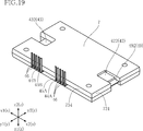
- FIG. 2 is a perspective view illustrating the semiconductor device according to the first embodiment.
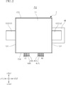
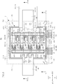
- FIG. 2 is a plan view illustrating the semiconductor device according to the first embodiment. In the plan view shown in FIG. 2, the sealing resin is omitted. It is the elements on larger scale which expanded a part of FIG.
- FIG. 2 is a front view illustrating the semiconductor device according to the first embodiment.
- FIG. 2 is a bottom view showing the semiconductor device according to the first embodiment.
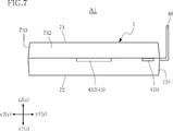
- FIG. 2 is a left side view illustrating the semiconductor device according to the first embodiment.
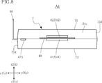
- FIG. 2 is a right side view illustrating the semiconductor device according to the first embodiment.
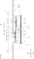
- FIG. 14 is a sectional view taken along the line IX-IX of FIG. 3.
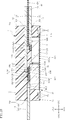
- FIG. 4 is a sectional view taken along line XX of FIG. 3.
- FIG. 3 is a view illustrating one step (first pressurizing and heating step) of the method for manufacturing a semiconductor device according to the first embodiment.
- FIG. 3 is a view illustrating one step (first pressurizing and heating step) of the method for manufacturing a semiconductor device according to the first embodiment.
- FIG. 5 is a view illustrating one step (second pressurizing and heating step) of the method for manufacturing a semiconductor device according to the first embodiment.
- FIG. 6 is a view illustrating one step (a first pressurizing and heating step) of another method of manufacturing the semiconductor device according to the first embodiment.
- FIG. 5 is a cross-sectional view illustrating a semiconductor device according to a modification of the first embodiment.
- FIG. 5 is a cross-sectional view illustrating a semiconductor device according to a modification of the first embodiment.
- FIG. 5 is a cross-sectional view illustrating a semiconductor device according to a modification of the first embodiment.
- FIG. 5 is a cross-sectional view illustrating a semiconductor device according to a modification of the first embodiment.
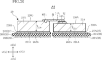
- FIG. 6 is a cross-sectional view of a main part showing a semiconductor device according to a second embodiment.
- FIG. 14 is a cross-sectional view of a principal part showing a semiconductor device according to a modification of the second embodiment.
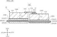
- FIG. 11 is a cross-sectional view of a main part showing a semiconductor device according to a third embodiment.
- FIG. 14 is a cross-sectional view of a principal part showing a semiconductor device according to a modification of the third embodiment.
- FIG. 14 is a cross-sectional view of a principal part showing a semiconductor device according to a fourth embodiment.
- FIG. 14 is a cross-sectional view of a principal part showing a semiconductor device according to a modification of the fourth embodiment.
- FIG. 14 is a cross-sectional view of a principal part showing a semiconductor device according to a fifth embodiment.
- FIG. 14 is a plan view illustrating a semiconductor device according to a sixth embodiment, in which a sealing resin is omitted.
- FIG. 28 is a cross-sectional view of FIG. 27 taken along the line XXVIII-XXVIII.
- an object A is formed on an object B” and “an object A is formed on an object B” mean “an object A is present,” unless otherwise specified. And that the object A is formed on the object B while another object is interposed between the object A and the object B. Similarly, “an object A is disposed on an object B” and “an object A is disposed on an object B” are “an object having an object A” unless otherwise specified. B "and" the object A is arranged on the object B while another is interposed between the object A and the object B ". Similarly, "an object A is located on an object B” means “an object A is in contact with an object B and an object A is located on the object B" unless otherwise specified.
- an object A is located on an object B while another is interposed between the object A and the object B.
- an object A is stacked on an object B” and “an object A is stacked on an object B” are “an object A is on an object B” unless otherwise specified.
- B directly “and” the thing A is stacked on the thing B while another is interposed between the certain thing A and the certain thing B ".
- an object A overlaps with an object B in a certain direction means “an object A overlaps all the objects B” unless otherwise specified, and “an object A overlaps with all the objects B”. Overlapping part of an object B ".
- the semiconductor device A1 according to the first embodiment includes a plurality of semiconductor elements 10, a support substrate 20, a plurality of conductive bonding layers 3, input terminals 41 and 42, an output terminal 43, a pair of gate terminals 44A and 44B, and a pair of detection terminals.
- the input terminals 41 and 42, the output terminal 43, a pair of gate terminals 44A and 44B, a pair of detection terminals 45A and 45B, a plurality of dummy terminals 46, and a pair of side terminals 47A and 47B are collectively referred to as a terminal 40. There is that.
- FIG. 1 is a perspective view showing the semiconductor device A1.
- FIG. 2 is a plan view showing the semiconductor device A1.
- FIG. 3 is a view in which the sealing resin 7 is omitted from the plan view shown in FIG. In FIG. 3, the sealing resin 7 is indicated by an imaginary line (two-dot chain line).
- FIG. 4 is a partially enlarged view in which a part of FIG. 3 is enlarged.
- FIG. 5 is a front view showing the semiconductor device A1.
- FIG. 6 is a bottom view showing the semiconductor device A1.
- FIG. 7 is a side view (left side view) showing the semiconductor device A1.
- FIG. 8 is a side view (right side view) showing the semiconductor device A1.
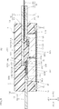
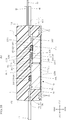
- FIG. 9 is a sectional view taken along line IX-IX in FIG.
- FIG. 10 is a sectional view taken along line XX of FIG.
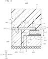
- FIG. 11 is a partially enlarged view in which a part of FIG. 10 is enlarged.
- the wire member 6 is
- the width direction x is a horizontal direction in a plan view (see FIGS. 2 and 3) of the semiconductor device A1.
- the depth direction y is a vertical direction in a plan view of the semiconductor device A1 (see FIGS. 2 and 3). If necessary, one in the width direction x is referred to as a width direction x1, and the other in the width direction x is referred to as a width direction x2.
- the thickness direction z1 may be referred to as lower and the thickness direction z2 may be referred to as upper.
- the dimension in the thickness direction z may be referred to as “thickness” or “thickness”.
- the thickness direction z corresponds to a “first direction” described in the claims.
- the width direction x corresponds to the “second direction” described in the claims.
- Each of the plurality of semiconductor elements 10 is configured using a semiconductor material mainly containing SiC (silicon carbide).
- the semiconductor material is not limited to SiC, but may be Si (silicon), GaAs (gallium arsenide), GaN (gallium nitride), or the like.
- each semiconductor element 10 is a MOSFET (Metal-Oxide-Semiconductor Field-Effect Transistor).
- the plurality of semiconductor elements 10 are not limited to MOSFETs, but include field effect transistors including MISFETs (Metal-Insulator-Semiconductor FETs), bipolar transistors such as IGBTs (Insulated Gate Bipolar Transistors), IC chips such as LSIs, and the like. It may be a diode, a capacitor, or the like. In the present embodiment, a case is shown in which each of the semiconductor elements 10 is the same element and is an n-channel MOSFET. Each semiconductor element 10 has a rectangular shape when viewed in the thickness direction z (hereinafter, also referred to as “plan view”), but is not limited thereto. Each semiconductor element 10 has a thickness of about 50 to 370 ⁇ m. The thickness of each semiconductor element 10 is not limited to this.
- Each of the plurality of semiconductor elements 10 has an element main surface 101 and an element back surface 102 as shown in FIG.
- FIG. 11 shows the semiconductor element 10A
- the semiconductor element 10B has the same configuration.
- the element main surface 101 and the element back surface 102 are separated from each other in the thickness direction z, and face the opposite sides.
- the element main surface 101 faces the thickness direction z2
- the element back surface 102 faces the thickness direction z1.
- Each of the plurality of semiconductor elements 10 has a main surface electrode 11, a back surface electrode 12, and an insulating film 13, as shown in FIG.
- the main surface electrode 11 is provided on the element main surface 101.
- the main surface electrode 11 includes a first electrode 111 and a second electrode 112, as shown in FIGS.
- the first electrode 111 is a source electrode, through which a source current flows.
- the second electrode 112 is a gate electrode to which a gate voltage for driving each semiconductor element 10 is applied.
- the first electrode 111 is larger than the second electrode 112. Further, in the present embodiment, the case where the first electrode 111 is configured by one region is shown, but the first electrode 111 may be divided into a plurality of regions.
- the back electrode 12 is provided on the back surface 102 of the element. In the present embodiment, the back surface electrode 12 is formed over the entire back surface 102 of the element. In the present embodiment, the back surface electrode 12 is a drain electrode, through which a drain current flows.
- the insulating film 13 is provided on the element main surface 101 as shown in FIG.
- the insulating film 13 has electric insulation.
- the insulating film 13 surrounds the main surface electrode 11 in plan view.
- the insulating film 13 insulates the first electrode 111 from the second electrode 112.
- the insulating film 13 is formed, for example, by stacking an SiO 2 (silicon dioxide) layer, a SiN 4 (silicon nitride) layer, and a polybenzoxazole layer in this order from the element main surface 101.
- a polyimide layer may be used instead of the polybenzoxazole layer.
- the configuration of the insulating film 13 is not limited to the above.
- the plurality of semiconductor elements 10 include the plurality of semiconductor elements 10A and the plurality of semiconductor elements 10B.
- the semiconductor device A1 forms a half-bridge type switching circuit.
- the plurality of semiconductor elements 10A constitute an upper arm circuit in the switching circuit
- the plurality of semiconductor elements 10B constitute a lower arm circuit in the switching circuit.
- the semiconductor device A1 includes four semiconductor elements 10A and four semiconductor elements 10B. Note that the number of the semiconductor elements 10 is not limited to this configuration, and can be freely set according to the performance required for the semiconductor device A1.
- Each of the plurality of semiconductor elements 10A is mounted on a support substrate 20 (a conductive substrate 22A described later) as shown in FIGS. 3, 4, 10, and 11.
- the plurality of semiconductor elements 10A are arranged in the depth direction y and are separated from each other.
- the element back surface 102 faces the conductive substrate 22A.
- Each of the semiconductor elements 10A is electrically connected to the support substrate 20 (conductive substrate 22A) via the conductive bonding layer 3 (element bonding layer 31A described later) as shown in FIGS. 3, 4, 10, and 11. Are joined.
- each of the semiconductor elements 10A entirely overlaps the conductive substrate 22B.
- Each of the plurality of semiconductor elements 10B is mounted on a support substrate 20 (a conductive substrate 22B described later), as shown in FIGS. 3, 4, and 9.
- the plurality of semiconductor elements 10B are arranged in the depth direction y and are separated from each other.
- the element back surface 102 faces the conductive substrate 22B.
- Each of the semiconductor elements 10B is conductively connected to the support substrate 20 (conductive substrate 22B) via the conductive bonding layer 3 (element bonding layer 31B described later), as shown in FIGS. I have.
- the plurality of semiconductor elements 10A and the plurality of semiconductor elements 10B are alternately arranged in the width direction x, but the plurality of semiconductor elements 10A and the plurality of semiconductor elements are viewed in the width direction x.
- the elements may be arranged so as to overlap with the element 10B.
- the support substrate 20 is a support member that supports the plurality of semiconductor elements 10.
- the support substrate 20 includes an insulating substrate 21, a plurality of conductive substrates 22, a pair of insulating layers 23A and 23B, a pair of gate layers 24A and 24B, and a pair of detecting layers 25A and 25B.
- the insulating substrate 21 has a plurality of conductive substrates 22 arranged thereon.
- the insulating substrate 21 has an electrical insulating property.
- the constituent material of the insulating substrate 21 is, for example, ceramics having excellent thermal conductivity. Examples of such ceramics include AlN (aluminum nitride), SiN (silicon nitride), and Al 2 O 3 (aluminum oxide).
- the insulating substrate 21 has a rectangular shape in plan view, as shown in FIG. Further, the insulating substrate 21 is in the shape of one flat plate. In the present embodiment, the insulating substrate 21 corresponds to an “insulating member” described in the claims.
- the insulating substrate 21 has a main surface 211 and a back surface 212 as shown in FIGS.
- the main surface 211 and the back surface 212 are separated from each other in the thickness direction z, and face opposite sides.
- the main surface 211 faces the side where the plurality of conductive substrates 22 are arranged in the thickness direction z, that is, the thickness direction z2.
- the main surface 211 is covered with the sealing resin 7 together with the plurality of conductive substrates 22 and the plurality of semiconductor elements 10.
- the back surface 212 faces the thickness direction z1.
- the back surface 212 is exposed from the sealing resin 7 as shown in FIGS. 6, 9 and 10.
- a heat sink (not shown) can be connected to the back surface 212.
- the configuration of the insulating substrate 21 is not limited to the above, and may be provided separately for each of the plurality of conductive substrates 22.
- the main surface 211 corresponds to the “insulating member main surface” described in the claims.
- each of the plurality of conductive substrates 22 is a plate member having conductivity.
- the constituent material of each conductive substrate 22 is copper or a copper alloy. That is, each conductive substrate 22 is a copper substrate.
- each conductive substrate 22 may be a composite substrate having a graphite substrate and a copper material formed on both surfaces in the thickness direction z of the graphite substrate. The surface of each conductive substrate 22 may be covered with silver plating.
- the plurality of conductive substrates 22 form a conduction path to the plurality of semiconductor elements 10 together with the plurality of terminals 40.
- the plurality of conductive substrates 22 are separated from each other, and each is disposed on the main surface 211 of the insulating substrate 21.
- the plurality of conductive substrates 22 include a conductive substrate 22A and a conductive substrate 22B.
- the conductive substrates 22A and 22B are separated from each other in the width direction x and are arranged on the insulating substrate 21, as shown in FIGS. 3, 9, 10, and 11. Further, both the conductive substrates 22A and 22B have a rectangular shape in plan view, as shown in FIG.
- the conductive substrate 22A is joined to the main surface 211 of the insulating substrate 21 via a joining material 220A, as shown in FIGS.
- the joining material 220A may be a conductive material such as a silver paste, a solder, or a sintered metal material, or may be an insulating material.
- the conductive substrate 22A is positioned in the width direction x2 more than the conductive substrate 22B.
- the conductive substrate 22A has a main surface 221A facing the thickness direction z2 as shown in FIGS. 9, 10, and 11, and a plurality of semiconductor elements 10A are mounted on the main surface 221A.
- the conductive substrate 22A when viewed in the width direction x, entirely overlaps the conductive substrate 22B.
- Dimension T 22A in the thickness direction z of the conductive substrate 22A is approximately 0.4 ⁇ 3.0 mm.
- the conductive substrate 22A corresponds to a “first electrode member” and a “first conductive substrate” described in the claims.
- the main surface 221A corresponds to a “first main surface” described in the claims, and the bonding material 220A corresponds to a “first bonding material” described in the claims.
- the conductive substrate 22B is joined to the main surface 211 of the insulating substrate 21 via a joining material 220B as shown in FIGS. 9, 10, and 11.
- the bonding material 220B may be a conductive material such as a silver paste, a solder, or a sintered metal, or may be an insulating material.
- the conductive substrate 22B has a main surface 221B facing the thickness direction z2, and a plurality of semiconductor elements 10B are mounted on the main surface 221B.
- One end of each of the plurality of lead members 51 is joined to the main surface 221B.
- Dimension T 22B in the thickness direction z of the conductive substrate 22B is approximately 0.4 ⁇ 3.0 mm.
- the conductive substrate 22B corresponds to a “second electrode member” and a “second conductive substrate” described in the claims.
- the main surface 221B corresponds to a “second main surface” described in the claims, and the bonding material 220B corresponds to a “second bonding material” described in the claims.
- the support substrate 20 has a step in the thickness direction z.
- the distance ⁇ T1 (see FIG. 11) in the thickness direction z between the main surface 221A and the main surface 221B is approximately 100 to 500 ⁇ m.
- the distance ⁇ T1 is provided by changing the dimension of the conductive substrate 22A and the conductive substrate 22B in the thickness direction z.
- the dimensional difference between the dimensions T 22B in the thickness direction z of dimension T 22A and the conductive substrate 22B in the thickness direction z of the conductive substrate 22A is approximately 100 ⁇ 500 [mu] m.
- the separation distance ⁇ T1 corresponds to the sum of the dimension of each semiconductor element 10 in the thickness direction z, the dimension of the element bonding layer 31A in the thickness direction z, and the dimension of the lead bonding layer 32 in the thickness direction z. Therefore, when the thickness of each semiconductor element 10 is large, the separation distance ⁇ T1 is increased, and when the thickness of each semiconductor element 10 is small, the separation distance ⁇ T1 is reduced. In the same manner, in each of the element bonding layers 31A and each of the lead bonding layers 32, the separation distance ⁇ T1 may be changed according to their thickness.
- the pair of insulating layers 23A and 23B have electric insulation, and the constituent material thereof is, for example, glass epoxy resin. As shown in FIG. 3, each of the pair of insulating layers 23A and 23B has a band shape extending in the depth direction y.
- the insulating layer 23A is joined to the main surface 221A of the conductive substrate 22A as shown in FIGS. 3, 9, and 10.
- the insulating layer 23A is located in the width direction x2 more than the plurality of semiconductor elements 10A.
- the insulating layer 23B is joined to the main surface 221B of the conductive substrate 22B as shown in FIGS. 3, 9, and 10.
- the insulating layer 23B is located in the width direction x1 more than the semiconductor element 10B.
- the pair of gate layers 24A and 24B have conductivity, and the constituent material thereof is, for example, copper or a copper alloy. As shown in FIG. 3, each of the pair of gate layers 24A and 24B has a band shape extending in the depth direction y.
- the gate layer 24A is disposed on the insulating layer 23A as shown in FIGS. 3, 9, and 10.
- the gate layer 24A conducts to the second electrode 112 (gate electrode) of each semiconductor element 10A via the wire member 6 (gate wire 61 described later).
- the gate layer 24B is disposed on the insulating layer 23B as shown in FIGS. 3, 9, and 10.
- the gate layer 24B conducts to the second electrode 112 (gate electrode) of each semiconductor element 10B via the wire member 6 (gate wire 61 described later).
- the pair of detection layers 25A and 25B have conductivity, and the constituent material is, for example, copper or a copper alloy. As shown in FIG. 3, each of the pair of detection layers 25A and 25B has a band shape extending in the depth direction y.
- the detection layer 25A is arranged on the insulating layer 23A together with the gate layer 24A as shown in FIGS. 3, 9, and 10.
- the detection layer 25A is located adjacent to the gate layer 24A on the insulating layer 23A in plan view and is separated from the gate layer 24A.
- the detection layer 25A is arranged closer to the plurality of semiconductor elements 10A than the gate layer 24A in the width direction x. Therefore, the detection layer 25A is located on the width direction x1 side of the gate layer 24A.
- the detection layer 25A is electrically connected to the first electrode 111 (source electrode) of each semiconductor element 10A via the wire member 6 (detection wire 62 described later).
- the detection layer 25B is arranged on the insulating layer 23B together with the gate layer 24B, as shown in FIGS.
- the detection layer 25B is located next to the gate layer 24B on the insulating layer 23B in plan view and is separated from the gate layer 24B.
- the detection layer 25B is arranged closer to the plurality of semiconductor elements 10B than the gate layer 24B. Therefore, the detection layer 25B is located on the width direction x2 side of the gate layer 24B.
- the detection layer 25B is electrically connected to the first electrode 111 (source electrode) of each semiconductor element 10B via the wire member 6 (detection wire 62 described later).
- Each of the plurality of conductive bonding layers 3 is made of a sintered metal formed by a sintering process.
- the constituent material of each conductive bonding layer 3 is sintered silver in the present embodiment, but is not limited thereto, and may be another sintered metal such as sintered copper.
- Each conductive bonding layer 3 is porous having a large number of micropores, and in the present embodiment, the micropores are voids.
- the micropores may be filled with, for example, an epoxy resin. That is, each conductive bonding layer 3 may be a sintered metal containing an epoxy resin. However, when the content of the epoxy resin is large, the conductivity of the conductive bonding layer 3 is reduced.
- the conductive bonding layer 3 can be formed by sintering a metal material for sintering.
- each conductive bonding layer 3 is formed with a fillet, for example, as shown in FIG. Note that a fillet may not be formed in each conductive bonding layer 3.
- the plurality of conductive bonding layers 3 include a plurality of element bonding layers 31A and 31B, a plurality of lead bonding layers 32, and a plurality of block bonding layers 33.
- Each of the plurality of element bonding layers 31A is for bonding each semiconductor element 10A to the conductive substrate 22A.
- Each element bonding layer 31A is interposed between the element back surface 102 of each semiconductor element 10A and the conductive substrate 22A, and electrically connects the back electrode 12 of the semiconductor element 10A and the conductive substrate 22A.
- Each element bonding layer 31A has a thickness of about 20 to 80 ⁇ m. The thickness is a dimension z in the thickness direction of a portion interposed between the semiconductor element 10A and the conductive substrate 22A. The thickness of each element bonding layer 31A is not limited to this. When viewed in the width direction x, each of the element bonding layers 31A entirely overlaps the conductive substrate 22B.
- Each of the plurality of element bonding layers 31B is for bonding each semiconductor element 10B to the conductive substrate 22B.
- Each element bonding layer 31B is interposed between the element back surface 102 of each semiconductor element 10B and the conductive substrate 22B, and electrically connects the back electrode 12 of the semiconductor element 10B and the conductive substrate 22B.
- Each element bonding layer 31B has a thickness of about 20 to 80 ⁇ m, similarly to each element bonding layer 31A. The thickness is a dimension z in the thickness direction of a portion interposed between the semiconductor element 10B and the conductive substrate 22B. The thickness of each element bonding layer 31B is not limited to this.
- Each of the plurality of lead bonding layers 32 is for bonding a part of each lead member 51 to each semiconductor element 10A. Specifically, each lead bonding layer 32 is interposed between the element main surface 101 of each semiconductor element 10A and a part (first bonding portion 511 described later) of each lead member 51, and The main surface electrode 11 (first electrode 111) and the lead member 51 are electrically connected.
- Each lead bonding layer 32 has a thickness of about 20 to 80 ⁇ m. The thickness is a dimension z in the thickness direction of a portion interposed between the semiconductor element 10A and the lead member 51. Note that the thickness of each lead bonding layer 32 is not limited to this.
- Each lead bonding layer 32 overlaps the conductive substrate 22B except for the fillet when viewed in the width direction x. In the present embodiment, the lead bonding layer 32 corresponds to a “conductive bonding layer” described in the claims.
- the plurality of block bonding layers 33 are for bonding the plurality of block electrodes 48 to the respective semiconductor elements 10B. Specifically, each block bonding layer 33 is interposed between the element main surface 101 of each semiconductor element 10B and the surface of each block bonding layer 33 that faces the thickness direction z2, and the main surface electrode of the semiconductor element 10B. 11 (the first electrode 111) and the block electrode 48 are conducted. Each block bonding layer 33 has a thickness of about 20 to 80 ⁇ m. The thickness is a dimension z in the thickness direction of a portion interposed between the semiconductor element 10B and the block electrode 48. The thickness of each block bonding layer 33 is not limited to this.
- the two input terminals 41 and 42 are each a metal plate.
- the constituent material of the metal plate is copper or a copper alloy.
- the two input terminals 41 and 42 both have a dimension in the thickness direction z of about 0.8 mm, but are not limited thereto.
- the two input terminals 41 and 42 are both located closer to the width direction x2 in the semiconductor device A1, as shown in FIG. 3, FIG. 9, and FIG.
- a power supply voltage is applied between the two input terminals 41 and 42.
- a power supply voltage may be directly applied from a power supply (not shown) to the input terminals 41 and 42, or a bus bar (not shown) may be connected so as to sandwich the input terminals 41 and 42, and the bus bars may be connected to the input terminals 41 and 42.
- the input terminal 41 is a positive electrode (P terminal), and the input terminal 42 is a negative electrode (N terminal).
- the input terminal 42 is spaced apart from both the input terminal 41 and the conductive substrate 22A in the thickness direction z.
- the input terminal 41 has a pad portion 411 and a terminal portion 412 as shown in FIGS.
- the pad portion 411 is a portion of the input terminal 41 that is covered with the sealing resin 7.
- An end portion of the pad portion 411 on the side in the width direction x1 has a comb shape, and includes a plurality of comb portions 411a.
- the pad section 411 may not include the plurality of comb teeth sections 411a and may be rectangular in plan view.
- Each of the plurality of comb teeth portions 411a is conductively joined to the main surface 221A of the conductive substrate 22A.
- each comb tooth portion 411a of the pad portion 411 is joined to the conductive substrate 22A by a welding method using a laser beam (hereinafter, referred to as “laser welding”).
- the laser beam in the present embodiment is not particularly limited, but is, for example, a green YAG laser.
- the bonding between each comb tooth portion 411a and the conductive substrate 22A may not be performed by laser welding but may be ultrasonic bonding or bonding using a conductive bonding material.
- a welding mark M41 is formed as shown in FIGS.
- the terminal portion 412 is a portion of the input terminal 41 that is exposed from the sealing resin 7. As shown in FIGS. 3, 5, 6, 8, and 9, the terminal portion 412 extends in the width direction x2 from the sealing resin 7 in plan view.
- the input terminal 42 has a pad 421 and a terminal 422 as shown in FIGS.
- the pad portion 421 is a portion of the input terminal 42 that is covered with the sealing resin 7.
- the pad section 421 includes a connecting section 421a and a plurality of extending sections 421b.
- the connecting portion 421a has a band shape extending in the depth direction y.
- the connection part 421a is connected to the terminal part 422.
- the plurality of extending portions 421b have a band shape extending from the connecting portion 421a in the width direction x1. In the present embodiment, each extension portion 421b extends from the connection portion 421a until it overlaps the semiconductor element 10B in plan view.
- the plurality of extending portions 421b are arranged in the depth direction y in plan view and are separated from each other.
- Each extension portion 421b has a tip portion overlapping with each block electrode 48 in a plan view.
- the tip portion is joined to the block electrode 48 by laser welding using laser light.
- the distal end portion is an end portion on the width direction x1 side of the extension portion 421b on the side opposite to the side connected to the connection portion 421a in the width direction x.
- the joining between each extension portion 421b and each block electrode 48 may be not by laser welding, but may be ultrasonic joining, or may be joining using a conductive joining material. In the case of joining by laser welding, as shown in FIGS. 3, 4, and 9, a welding mark M42 is formed.
- the terminal portion 422 is a portion of the input terminal 42 exposed from the sealing resin 7. 3,, 8, and 9, the terminal portion 422 extends in the width direction x2 from the sealing resin 7 in plan view.
- the terminal portion 422 has a rectangular shape in plan view.
- the terminal portion 422 overlaps with the terminal portion 412 of the input terminal 41 in plan view, as shown in FIGS. 3, 8, and 9.
- the terminal portion 422 is separated from the terminal portion 412 in the thickness direction z2.
- the shape of the terminal portion 422 is the same as the shape of the terminal portion 412.
- the output terminal 43 is a metal plate.
- the constituent material of the metal plate is, for example, copper or a copper alloy.
- the output terminal 43 is located closer to the width direction x1 in the semiconductor device A1, as shown in FIGS.
- the AC power (voltage) power-converted by the plurality of semiconductor elements 10 is output from the output terminal 43.
- the output terminal 43 includes a pad portion 431 and a terminal portion 432, as shown in FIGS.
- the pad portion 431 is a portion of the output terminal 43 that is covered with the sealing resin 7.
- the portion on the width direction x2 side of the pad portion 431 has a comb shape and includes a plurality of comb portions 431a. Note that the pad portion 431 does not include the plurality of comb teeth portions 431a, and may be rectangular in plan view.
- Each of the plurality of comb teeth portions 431a is conductively joined to the main surface 221B of the conductive substrate 22B. In the present embodiment, each comb tooth portion 431a of the pad portion 431 is joined to the conductive substrate 22B by laser welding using laser light.
- each of the comb teeth portions 431a and the conductive substrate 22B may not be performed by laser welding, but may be performed by ultrasonic bonding or bonding using a conductive bonding material.
- a welding mark M43 is formed as shown in FIGS.
- the terminal portion 432 is a portion of the output terminal 43 exposed from the sealing resin 7.
- the terminal portion 432 extends from the sealing resin 7 in the width direction x1, as shown in FIGS. 3, 5, 6, 7, and 9.
- the pair of gate terminals 44A, 44B are located adjacent to the conductive substrates 22A, 22B in the depth direction y, as shown in FIGS.
- a gate voltage for driving the plurality of semiconductor elements 10A is applied to the gate terminal 44A.
- a gate voltage for driving the plurality of semiconductor elements 10B is applied to the gate terminal 44B.
- Both the pair of gate terminals 44A and 44B have a pad portion 441 and a terminal portion 442, as shown in FIGS.
- the pad portion 441 is covered with the sealing resin 7.
- each of the gate terminals 44A and 44B is supported by the sealing resin 7.
- the surface of the pad portion 441 may be plated with silver, for example.
- the terminal portion 442 is connected to the pad portion 441 and is exposed from the sealing resin 7.
- the terminal portion 442 has an L shape when viewed in the width direction x.
- the pair of detection terminals 45A and 45B are located adjacent to the pair of gate terminals 44A and 44B in the width direction x as shown in FIGS. From the detection terminal 45A, a voltage (a voltage corresponding to a source current) applied to each main surface electrode 11 (first electrode 111) of the plurality of semiconductor elements 10A is detected. From the detection terminal 45B, a voltage (a voltage corresponding to a source current) applied to each main surface electrode 11 (first electrode 111) of the plurality of semiconductor elements 10B is detected.
- Both the pair of detection terminals 45A and 45B have a pad portion 451 and a terminal portion 452, as shown in FIGS.
- the pad 451 is covered with the sealing resin 7.
- each of the detection terminals 45A and 45B is supported by the sealing resin 7.
- the surface of the pad portion 451 may be plated with, for example, silver.
- the terminal portion 452 is connected to the pad portion 451 and is exposed from the sealing resin 7.
- the terminal portion 452 has an L shape when viewed in the width direction x.
- the plurality of dummy terminals 46 are located on the opposite side of the pair of detection terminals 45A and 45B in the width direction x from the pair of gate terminals 44A and 44B.
- the number of the dummy terminals 46 is six. Of these, three dummy terminals 46 are located on one side in the width direction x (width direction x2). The remaining three dummy terminals 46 are located on the other side (width direction x1) in the width direction x.
- the plurality of dummy terminals 46 are not limited to the configuration described above. Further, a configuration without the plurality of dummy terminals 46 may be adopted.
- Each of the plurality of dummy terminals 46 has a pad portion 461 and a terminal portion 462, as shown in FIGS.
- the pad portion 461 is covered with the sealing resin 7.
- the surface of the pad portion 461 may be plated with, for example, silver.
- the terminal portion 462 is connected to the pad portion 461 and is exposed from the sealing resin 7.
- the terminal portion 462 has an L shape when viewed in the width direction x.
- the shape of the terminal portion 462 is the same as the shape of each terminal portion 442 of the pair of gate terminals 44A, 44B and the shape of each terminal portion 452 of the pair of detection terminals 45A, 45B.
- the pair of side terminals 47 ⁇ / b> A and 47 ⁇ / b> B are edge portions on the depth direction y ⁇ b> 1 side of the sealing resin 7 in plan view, and each end in the width direction x of the sealing resin 7. It overlaps the edge.
- the side terminal 47A is joined to the conductive substrate 22A, and is covered with the sealing resin 7 except for an end face facing the width direction x2.
- the side terminal 47B is joined to the conductive substrate 22B, and is covered with the sealing resin 7 except for an end surface facing the width direction x1. In the present embodiment, all of the side terminals 47A and 47B overlap the sealing resin 7 in plan view.
- the side terminals 47A and 47B are respectively joined to the conductive substrates 22A and 22B by laser welding using a laser beam. Note that the joining between the side terminal 47A and the conductive substrate 22A and the joining between the side terminal 47B and the conductive substrate 22B may not be performed by laser welding but may be ultrasonic bonding. Bonding using a conductive bonding material may be used. In the case of joining by laser welding, a welding mark M47 is formed as shown in FIGS. Each of the side terminals 47A and 47B is partially bent in a plan view, and the other is bent in the thickness direction z. The configuration of each of the side terminals 47A and 47B is not limited to this. For example, in plan view, they may extend until they respectively protrude from the sealing resin 7. Further, the semiconductor device A1 does not have to include the side terminals 47A and 47B.
- the pair of gate terminals 44A and 44B, the pair of detection terminals 45A and 45B, and the plurality of dummy terminals 46 are arranged along the width direction x in plan view as shown in FIGS.
- the pair of gate terminals 44A and 44B, the pair of detection terminals 45A and 45B, the plurality of dummy terminals 46, and the pair of side terminals 47A and 47B are all formed from the same lead frame.
- the plurality of block electrodes 48 are interposed between a part of the input terminal 42 and the element main surface 101 of each semiconductor element 10B, as shown in FIGS.
- the surface electrode 11 (first electrode 111) is electrically connected. Therefore, the input terminal 42 is electrically connected to the first electrode 111 of each semiconductor element 10B via the plurality of block electrodes 48.
- Each block electrode 48 is connected to the first electrode 111 of each semiconductor element 10B by the conductive bonding layer 3 (block bonding layer 33).
- Each block electrode 48 overlaps each semiconductor element 10 ⁇ / b> B and the distal end of the extension 42 b of the input terminal 42 in plan view.
- Each block electrode 48 is joined to the tip of each extension 421b of the input terminal 42 by laser joining.
- Each block electrode 48 has conductivity.
- each block electrode 48 has a prismatic shape whose shape in plan view is rectangular. Note that the shape of each block electrode 48 is not limited to this, and the shape in plan view may be a circular column.
- the insulating plate 49 has an electrical insulating property, and its constituent material is, for example, insulating paper.
- a part of the insulating plate 49 is a flat plate, and as shown in FIGS. 3, 5, 8, 9 and 10, the terminal portion 412 of the input terminal 41 and the terminal portion 412 of the input terminal 42 in the thickness direction z. It is sandwiched between terminal portions 422.
- the entire input terminal 41 overlaps the insulating plate 49.
- a part of the pad part 421 and the entire terminal part 422 overlap the insulating plate 49.
- the two input terminals 41 and 42 are insulated from each other by the insulating plate 49.
- a part of the insulating plate 49 (the part on the x1 side in the width direction) is covered with the sealing resin 7.
- the insulating plate 49 has an interposed portion 491 and an extended portion 492 as shown in FIGS.
- the interposition part 491 is interposed between the terminal part 412 of the input terminal 41 and the terminal part 422 of the input terminal 42 in the thickness direction z.
- the intervening portion 491 is entirely sandwiched between the terminal portion 412 and the terminal portion 422.
- the extension portion 492 extends from the interposition portion 491 further in the width direction x2 than the terminal portions 412 and 422.
- the plurality of lead members 51 connect each semiconductor element 10A and the conductive substrate 22B.
- the constituent material of each lead member 51 is, for example, copper. Note that the constituent material may be a clad material such as CIC.
- Each of the lead members 51 has a rectangular shape extending in the width direction x in a plan view, as shown in FIGS.
- Each lead member 51 is a flat connection member.
- each lead member 51 has a dimension (thickness) in the thickness direction z of about 160 to 250 ⁇ m. Note that the thickness of each lead member 51 is not limited to this.
- Each lead member 51 is disposed in a direction in which the thickness direction z2 faces the main surface 221B of the conductive substrate 22B.
- Each lead member 51 corresponds to a “connection member” described in the claims.
- Each lead member 51 includes a first joint 511, a second joint 512, and a connecting part 513.
- the first bonding portion 511 is a portion bonded to the main surface electrode 11 (first electrode 111) of the semiconductor element 10A via the conductive bonding layer 3 (lead bonding layer 32).
- the first bonding portion 511 overlaps the first electrode 111 of the semiconductor element 10A, the lead bonding layer 32, and the semiconductor element 10A in plan view.
- the second joint portion 512 is a portion joined to the conductive substrate 22B by laser welding.
- a welding mark M51 by laser welding is formed in the second joint portion 512.
- the connecting portion 513 is a portion connected to the first joint 511 and the second joint 512.
- the connecting portion 513 overlaps with both the first joint portion 511 and the second joint portion 512 when viewed in the width direction x.
- Each lead member 51 has a lead main surface 51a.
- the lead main surface 51a faces the thickness direction z2.
- the lead main surface 51a is substantially flat.
- the lead main surface 51a includes respective surfaces of the first joint portion 511, the second joint portion 512, and the connecting portion 513 that face the thickness direction z2.
- Each of the plurality of wire members 6 is a so-called bonding wire.
- Each wire member 6 has conductivity, and its constituent material is, for example, any of aluminum, gold, and copper.
- the plurality of wire members 6 include a plurality of gate wires 61, a plurality of detection wires 62, a pair of first connection wires 63, and a pair of second connection wires 64. Contains.
- each of the plurality of gate wires 61 is joined to the second electrode 112 (gate electrode) of each semiconductor element 10, and the other end is formed of a pair of gate layers 24A and 24B. It is joined to either.
- the plurality of gate wires 61 include those that make the second electrode 112 of each semiconductor element 10A conductive with the gate layer 24A and those that make the second electrode 112 of each semiconductor element 10B conductive with the gate layer 24B.
- each of the plurality of detection wires 62 is connected to the first electrode 111 (source electrode) of each semiconductor element 10, and the other end of each of the plurality of detection wires 62 is a pair of the detection layers 25A and 25B. It is joined to either.
- the plurality of detection wires 62 include a wire that connects the first electrode 111 of each semiconductor element 10A to the detection layer 25A and a wire that connects the first electrode 111 of each semiconductor element 10B to the detection layer 25B.
- one of the pair of first connection wires 63 connects the gate layer 24A and the gate terminal 44A, and the other connects the gate layer 24B and the gate terminal 44B.
- One of the first connection wires 63 has one end joined to the gate layer 24A and the other end joined to the pad portion 441 of the gate terminal 44A, and these are connected to each other.
- the other first connection wire 63 has one end joined to the gate layer 24B and the other end joined to the pad portion 441 of the gate terminal 44B, and these are connected to each other.
- one pair of the second connection wires 64 connects the detection layer 25A and the detection terminal 45A, and the other connects the detection layer 25B and the detection terminal 45B.
- One end of the second connection wire 64 is joined to the detection layer 25A, and the other end is joined to the pad 451 of the detection terminal 45A, and these are connected to each other.
- One end of the other second connection wire 64 is joined to the detection layer 25B, and the other end is joined to the pad portion 451 of the detection terminal 45B, and these are connected to each other.
- the sealing resin 7 includes a plurality of semiconductor elements 10, a part of the support substrate 20, a plurality of conductive bonding layers 3, and a part of each terminal 40. , The plurality of lead members 51 and the plurality of wire members 6.
- the constituent material of the sealing resin 7 is, for example, an epoxy resin.
- the sealing resin 7 has a resin main surface 71, a resin back surface 72, and a plurality of resin side surfaces 731 to 734.
- the resin main surface 71 and the resin back surface 72 are separated in the thickness direction z and face opposite sides.
- the resin main surface 71 faces the thickness direction z2, and the resin back surface 72 faces the thickness direction z1.
- the resin back surface 72 has a frame shape surrounding the back surface 212 of the insulating substrate 21 in plan view.
- the back surface 212 of the insulating substrate 21 is exposed from the resin back surface 72.
- Each of the plurality of resin side surfaces 731 to 734 is connected to both the resin main surface 71 and the resin back surface 72 and is sandwiched therebetween in the thickness direction z.
- the resin side surfaces 731 and 732 are separated from each other in the width direction x and face opposite sides.
- the resin side surface 731 faces the width direction x2, and the resin side surface 732 faces the width direction x1.
- the resin side surfaces 733 and 734 are separated from each other in the depth direction y and face opposite sides.
- the resin side surface 733 faces the depth direction y2, and the resin side surface 734 faces the depth direction y1.
- the sealing resin 7 includes a plurality of recesses 75 each of which is recessed from the resin back surface 72 in the thickness direction z, as shown in FIGS. 5, 6, 9, and 10. Note that the sealing resin 7 does not need to include these concave portions 75.
- Each of the plurality of recesses 75 extends in the depth direction y, and is connected from the edge in the depth direction y1 to the edge in the depth direction y2 of the resin back surface 72 in plan view.
- three recesses 75 are formed in the width direction x with the back surface 212 of the insulating substrate 21 interposed therebetween in plan view.
- the support substrate 20 is prepared.
- an insulating substrate 21 having a main surface 211, a conductive substrate 22A having a main surface 221A, and a conductive substrate 22B having a main surface 221B are prepared.
- the conductive substrate 22A and the conductive substrate 22B are metal plates having a rectangular shape in a plan view.
- the conductive substrates 22A and 22B have different dimensions in the thickness direction z, and the conductive substrate 22B is larger.
- the dimensional difference in the thickness direction z is approximately 100 to 500 ⁇ m.
- conductive substrate 22A is bonded onto main surface 211 of insulating substrate 21 using bonding material 220A, and conductive substrate 22B is bonded using bonding material 220B.
- the conductive substrates 22A and 22B have the main surfaces 221A and 221B of the conductive substrates 22A and 22B facing the same direction as the main surface 211 of the insulating substrate 21, and the conductive substrates 22A and 22B are separated from each other. And place it.
- Both conductive substrates 22A and 22B are arranged on main surface 211 of insulating substrate 21.
- a step occurs between the main surface 221A of the conductive substrate 22A and the main surface 221B of the conductive substrate 22B due to the dimensional difference in the thickness direction z described above.
- the distance between the main surface 211A and the main surface 211B in the thickness direction z is approximately 100 to 500 ⁇ m, which is the same as the thickness difference between the conductive substrates 22A and 22B.
- the pair of insulating layers 23A and 23B, the pair of gate layers 24A and 24B, and the pair of detection layers 25A and 25B are joined on the conductive substrates 22A and 22B.
- the conductive layer 22A may be bonded to the insulating substrate 21 after the insulating layer 23A, the gate layer 24A, and the detection layer 25A are bonded to the conductive substrate 22A.
- the conductive substrate 22B may be joined to the insulating substrate 21.
- each sintering metal material 301A is a base of the element bonding layer 31A.
- paste-like silver for sintering is used as each sintering metal material 301A.
- the paste-like silver for sintering is obtained by mixing micro-size or nano-size silver particles in a solvent.
- the sintering silver solvent does not contain (or hardly contains) an epoxy resin.
- each sintering metal material 301A is applied onto the conductive substrate 22A by, for example, screen printing using a mask. .
- the method for forming the plurality of metal materials for sintering 301A is not limited to the screen printing described above.
- the metal material for sintering 301A may be applied by a dispenser.
- the thickness of the applied sintering metal material 301A is approximately 50 to 300 ⁇ m.
- each sintering metal material 301A is heated at a temperature of about 140 ° C. for about 20 minutes. Note that the heating conditions are not limited to this. Thereby, the solvent of each sintering metal material 301A is vaporized.
- each semiconductor element 10A is placed on each of the plurality of metal materials for sintering 301A.
- each semiconductor element 10A is mounted on the conductive substrate 22A with the conductive substrate 22A and the element back surface 102 of the semiconductor element 10A facing each other. .
- the sintering metal material 302 is formed on each of the semiconductor elements 10A.
- the metal material for sintering 302 is a base of the lead bonding layer 32.
- preformed silver for sintering is used as each metal material 302 for sintering.
- the silver for sintering in the form of a preform is, for example, formed by drying the above-mentioned silver for sintering in a paste form and then forming it into a predetermined shape. After being formed into a predetermined shape, it may be subjected to a drying treatment.
- the plurality of sintering metal materials 302 are placed on the semiconductor elements 10A one by one.
- the thickness of the placed metal material for sintering 303 is about 20 to 140 ⁇ m.
- each semiconductor element 10A is connected to the conductive substrate 22B using the plurality of lead members 51.
- an end portion of one side (width direction x2 side) in the width direction x of each lead member 51 overlaps the sintering metal material 302 in plan view.
- the lead member 51 is placed so that the edge portion on the other side in the width direction x (the width direction x1 side) overlaps the conductive substrate 22B.
- each lead member 51 is placed in a posture substantially parallel to a plane (xy plane) orthogonal to the thickness direction z.
- each of the lead members 51 is pressed from the lead main surface 51 a side of each of the lead members 51 by the pressing member 80. This applies a pressing force to the plurality of metal materials for sintering 301A, 302.
- a cushioning material for example, made of carbon or Teflon (registered trademark) may be attached to the pressing surface of the pressing member 80.
- the pressing member 80 uniformly contacts the lead main surface 51a of each of the lead members 51. Then, the sintering metal materials 301A and 302 pressed through the lead member 51 are heated at a temperature of, for example, about 250 ° C. for about 90 seconds. Note that the heating conditions are not limited to this. As a result, in each of the plurality of sintering metal materials 301A and 302, the silver particles are bonded to each other to form a sintered metal.
- the sintering metal material 301A becomes the element bonding layer 31A of the conductive bonding layer 3
- the sintering metal material 302 becomes the lead bonding layer 32 of the conductive bonding layer 3.
- Fillets are formed in the element bonding layer 31A and the lead bonding layer 32.
- the sintering process is a combination of a drying process and a heating process under pressure when a paste-like metal material for sintering is used as a sintered metal. In the case where a sintered metal is used as the binding metal material, it means a pressurized heat treatment.
- each lead member 51 is joined to the conductive substrate 22B.
- the step of joining the lead members 51 is performed by laser welding.
- the laser beam used in the laser welding is not particularly limited, but is, for example, a green YAG laser.
- welding marks M51 are formed, and each lead member 51 and the conductive substrate 22B are conductively joined.
- each sintering metal material 301B is a base of the element bonding layer 31B.
- paste sintering silver is used as each sintering metal material 301B, similarly to each sintering metal material 301A.
- each sintering metal is formed by screen printing using a mask, for example, as in the first sintering metal material forming step.
- the material 301B is applied on the conductive substrate 22B.
- the method for forming the plurality of metal materials for sintering 301B is not limited to the screen printing described above.
- the sintering metal material 301B may be applied by a dispenser.
- the thickness of the applied metal material for sintering 301B is approximately 50 to 100 ⁇ m.
- each metal material for sintering 301B is heated at a temperature of about 140 ° C. for about 20 minutes. Note that the heating conditions are not limited to this. Thereby, the solvent of each sintering metal material 301B is vaporized.
- each semiconductor element 10B is placed on each of the plurality of metal materials for sintering 301B.
- each semiconductor element 10B is mounted on the conductive substrate 22B with the conductive substrate 22B and the element back surface 102 of the semiconductor element 10B facing each other. .
- the sintering metal material 303 is formed on each of the semiconductor elements 10B.
- the sintering metal material 303 is a base of the block bonding layer 33.
- a preform-shaped sintering silver is used as each of the sintering metal materials 303.
- a plurality of sintering metal materials 303 are respectively placed on the plurality of semiconductor elements 10B. Place them one by one.
- a fillet is formed on the sintering metal material 303, but the sintering metal material 303 after the fourth sintering metal material forming step has a cross-sectional shape parallel to the thickness direction z. Is a substantially rectangular shape.
- the thickness of the placed metal material for sintering 303 is about 20 to 140 ⁇ m.
- one block electrode 48 is placed on each of the plurality of metal materials 303 for sintering.
- the step of mounting the block electrode 48 is referred to as a block electrode mounting step.
- each block electrode 48 is pressed from above by a pressing member 81 different from the pressing member 80. Then, a pressing force is applied to the plurality of sintering metal materials 301B and 303. Note that the pressing member 80 and the pressing member 1 may be the same. Then, the pressurized sintering metal materials 301B and 303 are heated via the block electrode 48 at a temperature of, for example, about 250 ° C. for about 90 seconds. Note that the heating conditions are not limited to this.
- the silver particles are bonded to each other to form a sintered metal.
- the sintering metal material 301B becomes the element bonding layer 31B of the conductive bonding layer 3
- the sintering metal material 303 becomes the block bonding layer 33 of the conductive bonding layer 3. Fillets are formed in the element bonding layer 31B and the block bonding layer 33.
- the step of joining the terminals 40 includes the following processing.
- the order of the processing described below is not particularly limited.
- the comb teeth 411a are joined to the main surface 221A of the conductive substrate 22A.
- the joining may be joining by laser welding or ultrasonic joining.
- the comb teeth 431a are joined to the main surface 221B of the conductive substrate 22B.
- the joining may be joining by laser welding or ultrasonic joining.
- the input terminal 41 and the block electrode 48 are joined with the insulating plate 49 interposed therebetween.
- each edge portion of the plurality of extending portions 421b of the input terminal 42 abuts on each block electrode 48, and overlaps with each block electrode 48 in plan view.
- the joining with the insulating plate 49 is performed by an adhesive (not shown), and the joining with the block electrode 48 is performed by laser welding.
- the pair of gate terminals 44A and 44B, the pair of detection terminals 45A and 45B, the plurality of dummy terminals 46, and the pair of side terminals 47A and 47B are formed on one lead frame, and these are connected.
- portions of the lead frame corresponding to the side terminals 47A and 47B are joined to the main surface 221A of the conductive substrate 22A and the main surface 221B of the conductive substrate 22B, respectively.
- the joining may be joining by laser welding or ultrasonic joining.
- a plurality of wire members 6 are formed.
- a known wire bonder is used.
- a plurality of gate wires 61 connecting the second electrode 112 of each semiconductor element 10A and the gate layer 24A, and a plurality of gates connecting the second electrode 112 of each semiconductor element 10B and the gate layer 24B.
- the wire 61 is formed.
- a plurality of detection wires 62 connecting the first electrode 111 of each semiconductor element 10A and the detection layer 25A and a plurality of detection wires 62 connecting the first electrode 111 of each semiconductor element 10B and the detection layer 25B are formed.
- first connection wire 63 connecting the gate layer 24A and the gate terminal 44A and a first connection wire 63 connecting the gate layer 24B and the gate terminal 44B are formed.
- second connection wire 64 connecting the detection layer 25A and the detection terminal 45A and a second connection wire 64 connecting the detection layer 25B and the detection terminal 45B are formed.
- the order of forming the plurality of wire members 6 is not particularly limited.
- the sealing resin 7 is formed.
- transfer molding is performed.
- the sealing resin 7 is, for example, an epoxy resin.
- the plurality of semiconductor elements 10, a part of the support substrate 20, the plurality of conductive bonding layers 3, and a part of the plurality of terminals 40 are respectively covered so as to cover the plurality of lead members 51 and the plurality of wire members 6.
- a sealing resin 7 is formed. From the formed sealing resin 7, a part of each terminal 40 and a part of the support substrate 20 (specifically, the back surface 212 of the insulating substrate 21) are exposed.
- post-processing step unnecessary portions of the plurality of terminals 40 (for example, a part of the lead frame) are cut or the plurality of terminals 40 are bent.
- engraving and printing on the sealing resin 7 may be performed.
- the semiconductor device A1 shown in FIGS. 1 to 11 is manufactured. Note that the above manufacturing method is an example, and the present invention is not limited to this.
- the semiconductor element 10A bonded on the conductive substrate 22A and the conductive substrate 22B are electrically connected by the lead member 51.
- the conductive substrate 22A, the semiconductor element 10A, and the lead bonding layer 32 overlap the conductive substrate 22B when viewed in the width direction x.
- a step is provided between a mounting surface for mounting the semiconductor element 10A and a bonding surface for bonding the second bonding portion 512 of the lead member 51.
- the mounting surface for mounting the semiconductor element 10A is the main surface 221A of the conductive substrate 22A, and the bonding surface for bonding the second bonding portion 512 of the lead member 51 is formed on the conductive substrate 22B.
- the main surface 221B is the main surface 221B.
- the shape of the lead member 51 can be, for example, a flat plate shape that is not bent. Therefore, at the time of pressurizing in the pressurizing and heating step (sintering process), it is easy to press the lead main surface 51a of the lead member 51 uniformly. Therefore, since the bias of the degree of pressurization can be suppressed, it is possible to suppress the destruction of the semiconductor element 10A, the insufficient strength of the conductive bonding layer 3, and the like. As described above, a decrease in the reliability of the semiconductor device A1 can be suppressed.
- the flat lead member 51 is used. According to this configuration, since it is not necessary to bend the lead member 51, a manufacturing error in the shape of the lead member 51 is reduced. Therefore, the pressing force of the pressing member 80 on the lead member 51 can be suppressed from being uneven.
- the semiconductor device A1 the plurality of semiconductor elements 10A are mounted on the conductive substrate 22A formed of a metal plate, and the plurality of semiconductor elements 10B are mounted on the conductive substrate 22B formed of a metal plate.
- the conductive substrates 22A and 22B function as heat radiating plates for radiating heat generated when the semiconductor elements 10A and 10B are energized. Therefore, the semiconductor device A1 can improve the heat dissipation, so that a problem due to heat can be suppressed.
- each lead member 51 and the conductive substrate 22B are joined by laser welding in the lead joining step. Therefore, the second joint portion 512 of each lead member 51 is joined by laser welding.
- the heat generated by laser welding is local and does not spread widely.
- a conventional semiconductor device Patent Document 1
- both ends of a beam lead are joined using a sintered joining material.
- the sintered joining materials at both ends of the beam lead are simultaneously cured when the temperature is lowered after heating.
- the substrate may be warped by the stress applied at this time.
- one side of the lead member 51 is joined by laser welding.
- the semiconductor device A1 can suppress the warpage of the support substrate 20.
- the sintering metal material 301A formed under each of the semiconductor elements 10A and the sintering metal material 302 formed on each of the semiconductor elements 10A are simultaneously subjected to pressure and heat treatment. I have. That is, the element bonding layer 31A and the lead bonding layer 32 are simultaneously subjected to the sintering process in the first pressure heating step. Therefore, since the element bonding layer 31A and the lead bonding layer 32 are formed from the sintering metal materials 301A and 302 by one pressurizing and heating process, the productivity of the semiconductor device A1 can be improved. .
- the block electrode 48 is joined to the element main surface 101 of each semiconductor element 10B, and a part of the input terminal 42 (the tip of the extension 421b) is joined to the block electrode 48. ing.
- each lead member 51 can be separated from the extension 421b of the input terminal 42 in the thickness direction z. Therefore, an unintended short circuit can be suppressed.
- the sintering metal material 301B formed under each of the semiconductor elements 10B and the sintering metal material 303 formed on each of the semiconductor elements 10B are simultaneously subjected to the pressure and heat treatment.
- the element bonding layer 31B and the block bonding layer 33 are simultaneously subjected to the sintering process in the second pressure heating step. Therefore, the element bonding layer 31B and the block bonding layer 33 are formed from the metal materials for sintering 301B and 303 by a single pressurizing and heating process, so that the productivity of the semiconductor device A1 can be improved.
- the element bonding layers 31A and 31B are formed from the sintering metal materials 301A and 301B, which are paste-like sintering silver. Paste silver is less expensive than preform silver. Therefore, the manufacturing cost of the semiconductor device A1 can be reduced.
- the element bonding layers 31A and 31B may be formed from preformed silver for sintering. In other words, preformed silver for sintering may be used as the metal materials for sintering 301A and 301B. In this case, the manufacturing cost of the semiconductor device A1 increases, but the productivity can be improved because the above-described drying step becomes unnecessary.
- a jig for manufacturing the semiconductor device A1 may be used.
- the following method may be used.
- the first sintering metal material forming step, the first drying step, the first mounting step, and the second sintering metal material forming step are performed without bonding the conductive substrate 22B to the insulating substrate 21. I do.
- a jig 89 is placed at a place where the conductive substrate 22B is to be mounted, as shown in FIG.
- the jig 89 is larger than the region where the conductive substrate 22B is arranged, and covers a part of the main surface 221A of the conductive substrate 22A as shown in FIG. Thereafter, in the lead connection step, each lead member 51 is placed so that each lead member 51 straddles each semiconductor element 10A and the jig 89. Next, a first pressure and heat treatment is performed to join the semiconductor element 10A to the conductive substrate 22A and join each semiconductor element 10A to one end of each lead member 51. Next, the jig 89 is removed, the conductive substrate 22B is bonded onto the insulating substrate 21, and the other end of each lead member 51 is bonded to the conductive substrate 22B by the above-described lead bonding process.
- Subsequent steps are the same as the method of manufacturing the semiconductor device A1 according to the first embodiment. Accordingly, the space below the lead member 51 in the central portion in the width direction x can be reduced, so that the bending of each lead member 51 due to the pressing force of the pressing member 80 can be suppressed.
- the first pressurizing and heating step and the second pressurizing and heating step are performed separately has been described, but the present invention is not limited to this.
- the first pressure heating step and the second pressure heating step can be performed at once by changing the order of the steps of the above-described manufacturing method. Specifically, each step is performed in the following order. That is, a supporting substrate preparing step, a first sintering metal material forming step and a third sintering metal material forming step, a first drying step and a second drying step, a first mounting step and a second mounting step, and a second firing step.
- the forming step, the resin forming step, and the post-processing step are in this order.
- the first pressurizing and heating step and the second pressurizing and heating step can be performed at the same time, so that the productivity of the semiconductor device A1 can be improved.
- the first drying step and the second drying step can be performed at the same time, so that the productivity can be further improved.
- the support substrate 20 includes one insulating substrate 21 and the conductive substrates 22A and 22B are supported by the insulating substrate 21 has been described.
- the present invention is not limited to this.
- the supporting substrate 20 may include two insulating substrates 21A and 21B, the conductive substrate 22A may be supported by the insulating substrate 21A, and the conductive substrate 22B may be supported by the insulating substrate 21B.
- FIG. 16 shows a semiconductor device A1 'according to such a modification.
- the conductive substrate 22A is bonded to the insulating substrate 21A via the bonding material 220A as shown in FIG.
- the insulating substrate 21A has a main surface 211A facing the thickness direction z2, and the conductive substrate 22A is arranged on the main surface 211A.
- the conductive substrate 22B is joined to the insulating substrate 21B via a joining material 220B.
- the insulating substrate 21B has a main surface 211B facing the thickness direction z2, and the conductive substrate 22B is arranged on the main surface 211B.
- the combination of the insulating substrates 21A and 21B corresponds to the “insulating member” described in the claims.
- the combination of the main surfaces 211A and 211B corresponds to the “insulating member main surface” described in the claims.
- each comb tooth portion 411a each comb tooth portion 411a of the input terminal 41 is bent
- the tip portion of each comb tooth portion 411a may be thicker so as to protrude in the thickness direction z1.
- the input terminal 42 has a flat plate shape, and the input terminal 41, the insulating plate 49, and the input terminal 42 are arranged in a step difference and a thickness direction z ⁇ b> 1 as compared with the first embodiment. It may be.
- FIG. 19 is a perspective view showing a semiconductor device according to a modified example, which is a semiconductor device having a different shape of the sealing resin 7 as described above.
- each edge portion in the depth direction y extends in the width direction x.
- a portion of the sealing resin 7 extending in the width direction x2 covers a part of each of the two input terminals 41 and 42 and the insulating plate 49.
- a part of the output terminal 43 is covered by a part of the sealing resin 7 extending in the width direction x1. According to such a modification, for example, in the semiconductor device A1, the two input terminals 41 and 42, the output terminal 43, and a part of the insulating plate 49 protruding from the sealing resin 7 can be protected.
- FIG. 20 shows a semiconductor device according to the second embodiment.
- FIG. 20 is a cross-sectional view showing the semiconductor device A2 of the second embodiment, and corresponds to the cross section of the first embodiment shown in FIG.
- parts other than a part of the support substrate 20, the semiconductor element 10A, a part of the conductive bonding layer 3, and the lead member 51 are omitted. Those omitted are configured substantially the same as the first embodiment or its modified example.
- the semiconductor device A2 differs from the first embodiment in the configuration of the support substrate 20.
- the conductive substrates 22A and 22B are supported not on the insulating substrate 21 but on a structure called a DBC (Direct Bonded Copper) substrate.
- DBC Direct Bonded Copper
- the support substrate 20 of the present embodiment supports the conductive substrates 22A and 22B on a structure called a DBC substrate.
- the support substrate 20 includes an insulating substrate 26, a main surface metal layer 27, a back surface metal layer 28, and conductive substrates 22A and 22B.
- the insulating substrate 26 has electrical insulation.
- the constituent material of the insulating substrate 26 is ceramic as in the case of the insulating substrate 21.
- the constituent material is not limited to ceramics, but may be an insulating resin sheet or the like.
- the insulating substrate 26 includes insulating substrates 26A and 26B spaced apart from each other.
- the insulating substrate 26A has a main surface 261A and a back surface 262A that are separated from each other in the thickness direction z and face opposite sides.
- the main surface 261A faces in the same direction as the element main surface 101 of the semiconductor element 10A.
- the insulating substrate 26B has a main surface 261B and a back surface 262B that are separated from each other in the thickness direction z and face opposite sides.
- the main surface 261B faces in the same direction as the main surface 261A of the insulating substrate 26A.
- the thickness of the insulating substrate 26A is substantially the same as the thickness of the insulating substrate 26B.
- the insulating substrate 26A corresponds to a “first insulating substrate” described in the claims
- the insulating substrate 26B corresponds to a “second insulating substrate” described in the claims.
- the combination of the back surface 262A of the insulating substrate 26A and the back surface 262B of the insulating substrate 26B corresponds to the “insulating substrate back surface” described in the claims.
- the main surface metal layer 27 is formed so as to cover a part of the insulating substrate 26.
- the constituent material of the main surface metal layer 27 is copper. In the case of a DBA substrate, the constituent material is aluminum.
- the main surface metal layer 27 is covered with the sealing resin 7.
- the dimension of main surface metal layer 27 in the thickness direction z is approximately 200 to 400 ⁇ m.
- the main surface metal layer 27 includes main surface metal layers 27A and 27B separated from each other.
- the main surface metal layer 27A is formed on the main surface 261A of the insulating substrate 26A.
- the conductive substrate 22A is joined to the main surface metal layer 27A via a joining material 220A.
- the main surface metal layer 27B is formed on the main surface 261B of the insulating substrate 26B.
- the conductive substrate 22B is joined to the main surface metal layer 27B via a joining material 220B.
- the thickness of main surface metal layer 27A and the thickness of main surface metal layer 27B are substantially the same.
- the main surface metal layer 27A corresponds to the “first main surface metal layer” described in the claims
- the main surface metal layer 27B corresponds to the “second main surface metal layer” described in the claims. Layer).
- the back metal layer 28 is formed so as to cover at least a part of the back surface 262 of the insulating substrate 26.
- the constituent material of the back metal layer 28 is copper.
- the support substrate 20 is a DBA substrate, the constituent material is aluminum.
- the back metal layer 28 may be covered with the sealing resin 7, or a surface facing the thickness direction z ⁇ b> 1 may be exposed from the sealing resin 7.
- the size of the back metal layer 28 in the thickness direction z is approximately 200 to 400 ⁇ m.
- the back metal layer 28 includes back metal layers 28A and 28B.
- the back metal layer 28A covers at least a part of the back surface 262A of the insulating substrate 26A.
- the back metal layer 28B covers at least a part of the back surface 262B of the insulating substrate 26B.
- the thickness of the back metal layer 28A is substantially the same as the thickness of the back metal layer 28B.
- the thickness of the back metal layer 28A may be the same as or different from the thickness of the main metal layer 27A.
- the thickness of the back surface metal layer 28B may be the same as or different from the thickness of the main surface metal layer 27B.
- one DBC substrate is configured by the insulating substrate 26A, the main surface metal layer 27A, and the back surface metal layer 28A.
- one DBC substrate is constituted by the insulating substrate 26B, the main surface metal layer 27B, and the back surface metal layer 28B.
- the insulating substrates 26A and 26B have the same thickness and are arranged at substantially the same position in the thickness direction z.
- the insulating substrates 26A and 26B overlap each other when viewed in the width direction x.
- the main surface metal layers 27A and 27B have the same thickness, and are arranged at substantially the same position in the thickness direction z.
- the main surface metal layers 27A and 27B overlap each other when viewed in the width direction x.
- the back metal layers 28A and 28B have the same thickness and are arranged at substantially the same position in the thickness direction z.
- the back metal layers 28A and 28B overlap each other when viewed in the width direction x.
- the conductive substrates 22A and 22B have different thicknesses, as in the first embodiment, and the difference is about 100 to 500 ⁇ m. Therefore, in the present embodiment, by arranging two conductive substrates 22A and 22B having different thicknesses on two DBC substrates having the same thickness, respectively, the difference in the thickness of the conductive substrates 22A and 22B causes the supporting substrate to be different. At 20, a step is provided.
- the semiconductor element 10A joined to the conductive substrate 22A and the conductive substrate 22B are electrically connected by the lead member 51.
- the conductive substrate 22A, the semiconductor element 10A, and the lead bonding layer 32 overlap the conductive substrate 22B when viewed in the width direction x. Therefore, similarly to the semiconductor device A1, the semiconductor device A2 has a bonding surface (conductive surface) for bonding the mounting surface (the main surface 221A of the conductive substrate 22A) on which the semiconductor element 10A is mounted and the second bonding portion 512 of the lead member 51.
- a step can be provided on the main surface 221B) of the substrate 22B.
- the flat lead member 51 which is not bent can be used, it is easy to press the lead member 51 uniformly, and the bias of the degree of pressurization can be suppressed. Therefore, the destruction of the semiconductor element 10A and the insufficient strength of the conductive bonding layer 3 can be suppressed, so that a decrease in the reliability of the semiconductor device A2 can be suppressed.
- the insulating substrate 26 includes the two insulating substrates 26A and 26B
- the present invention is not limited to this.
- the insulating substrate 26A and the insulating substrate 26B may be integrated. That is, the supporting substrate 20 includes one insulating substrate 26, and the main surface metal layers 27 ⁇ / b> A and 27 ⁇ / b> B may be formed on the main surface 261 of the insulating substrate 26.
- main surface metal layers 27A and 27B are formed by patterning one main surface metal layer 27 formed on main surface 261 of insulating substrate 26. The method of patterning is not particularly limited, but is, for example, etching.
- the back metal layer 28A and the back metal layer 28B formed on the back surface 262 of the insulating substrate 26 may be integrated.
- the back surface 262 of the insulating substrate 26 corresponds to the “back surface of the insulating substrate” described in the claims.
- FIG. 22 shows a semiconductor device according to the third embodiment.
- FIG. 22 is a cross-sectional view illustrating a semiconductor device A3 according to the third embodiment, and corresponds to a cross section illustrated in FIG. 20 of the second embodiment. Therefore, also in FIG. 22, parts other than a part of the support substrate 20, the semiconductor element 10A, a part of the conductive bonding layer 3, and the lead member 51 are omitted.
- the semiconductor device A3 differs from the first embodiment and the second embodiment in the configuration of the support substrate 20.
- the semiconductor device A3 is different from the second embodiment in that the semiconductor device A3 does not include the conductive substrates 22A and 22B, and that the main surface metal layer 27 has a thickness and a main surface of the main surface metal layer 27A. The difference is that the thickness is different from that of the metal layer 27B.
- the support substrate 20 of the present embodiment includes insulating substrates 26A and 26B, main surface metal layers 27A and 27B, and back surface metal layers 28A and 28B.
- a plurality of semiconductor elements 10A are conductively connected via an element bonding layer 31A.
- the main surface metal layer 27A is electrically connected to the back surface electrode 12 (drain electrode) of each semiconductor element 10A.
- a P terminal (not shown) (corresponding to the input terminal 41) is connected to the main surface metal layer 27 ⁇ / b> A, and a part of the P terminal is exposed from the sealing resin 7.
- the main surface metal layer 27A corresponds to a “first electrode member” described in the claims.
- a plurality of lead members 51 are joined to the main surface metal layer 27B of this embodiment by laser welding.
- the main surface metal layer 27B is electrically connected to the first electrode 111 (source electrode) of the main surface electrode 11 of each semiconductor element 10A via each lead member 51. Further, the plurality of semiconductor elements 10B are conductively connected to the main surface metal layer 27B via the element bonding layer 31B.
- the main surface metal layer 27B conducts to the back surface electrode 12 (drain electrode) of each semiconductor element 10B.
- An output terminal (not shown) (corresponding to the output terminal 43) is connected to the main surface metal layer 27 ⁇ / b> B, and the output terminal is partially exposed from the sealing resin 7.
- the main surface metal layer 27B corresponds to a “second electrode member” described in the claims.
- the thickness of the main surface metal layer 27A is smaller than the thickness of the main surface metal layer 27B.
- These dimensional differences ⁇ T2 are approximately 100 to 500 ⁇ m.
- the semiconductor element 10A, the main surface metal layer 27A, and the lead bonding layer 32 overlap the main surface metal layer 27B when viewed in the width direction x.
- steps are provided in the support substrate 20 by changing the thicknesses of the main surface metal layers 27A and 27B as described above.
- the semiconductor element 10A joined to the main surface metal layer 27A of the main surface metal layer 27 and the main surface metal layer 27B of the main surface metal layer 27 are electrically connected by the lead member 51.
- the main surface metal layer 27A of the main surface metal layer 27, the semiconductor element 10A, and the lead bonding layer 32 overlap with the main surface metal layer 27B of the main surface metal layer 27 when viewed in the width direction x. Therefore, in the semiconductor device A3, similarly to the semiconductor device A1, a step can be provided between the mounting surface for mounting the semiconductor element 10A and the bonding surface for bonding the second bonding portion 512 of the lead member 51.
- the mounting surface on which the semiconductor element 10A is mounted is a surface facing the thickness direction z2 of the main surface metal layer 27A
- the bonding surface for bonding the second bonding portion 512 of the lead member 51 is This is a surface facing the thickness direction z2 of the main surface metal layer 27B.
- FIG. 23 shows a semiconductor device A3 'according to the modification.
- a conductive substrate 22A is formed on a main surface metal layer 27A
- a conductive substrate 22B is formed on a main surface metal layer 27B.
- the thickness of the conductive substrate 22A and the thickness of the conductive substrate 22B are the same.
- the insulating substrate 26A and the insulating substrate 26B may be integrated as in the semiconductor device A2 '.
- the back metal layer 28A and the back metal layer 28B may be integrated.
- FIG. 24 shows a semiconductor device according to the fourth embodiment.
- FIG. 24 is a cross-sectional view illustrating a semiconductor device A4 according to the fourth embodiment, and corresponds to a cross section illustrated in FIG. 20 of the second embodiment. Therefore, also in FIG. 24, a part other than a part of the support substrate 20, the semiconductor element 10A, a part of the conductive bonding layer 3, and the lead member 51 is omitted.
- the semiconductor device A4 differs from the first to third embodiments in the configuration of the support substrate 20. Specifically, in the semiconductor device A4, as compared with the third embodiment, not only the main surface metal layers 27A and 27B of the main surface metal layer 27 but also the back metal layers 28A and 28B of the back metal layer 28 Are different in thickness.
- the main surface metal layer 27A and the back surface metal layer 28A have substantially the same thickness, and the main surface metal layer 27B and the back surface metal layer 28B have substantially the same thickness.
- the thickness of main surface metal layer 27A and back metal layer 28A is different from the thickness of main surface metal layer 27B and back metal layer 28B.
- the thickness of the main surface metal layer 27B and the back surface metal layer 28B is larger than the thickness of the main surface metal layer 27A and the back surface metal layer 28A.
- the semiconductor element 10A bonded to the main surface metal layer 27A of the main surface metal layer 27 and the main surface metal layer 27B of the main surface metal layer 27 are electrically connected by the lead member 51. Further, a part of the main surface metal layer 27A of the main surface metal layer 27, the semiconductor element 10A and the lead bonding layer 32 overlap with the main surface metal layer 27B of the main surface metal layer 27 when viewed in the width direction x. Therefore, in the semiconductor device A4, the mounting surface (the surface facing the thickness direction z2 of the main surface metal layer 27A) on which the semiconductor element 10A is mounted and the second bonding portion 512 of the lead member 51 are bonded similarly to the semiconductor device A3.
- a step can be provided with the joining surface (the surface facing the thickness direction z2 of the main surface metal layer 27B).
- FIG. 25 shows a semiconductor device A4 'according to the modification.
- the conductive substrate 22A is formed on the main surface metal layer 27A
- the conductive substrate 22B is formed on the main surface metal layer 27B.
- the thickness of the conductive substrate 22A and the thickness of the conductive substrate 22B are the same.
- the conductive substrate 22A corresponds to a “first electrode member” described in the claims
- the conductive substrate 22B corresponds to a “second electrode member” described in the claims.
- FIG. 26 shows a semiconductor device according to the fifth embodiment.
- FIG. 26 is a cross-sectional view illustrating a semiconductor device A5 according to the fifth embodiment, and corresponds to the cross section illustrated in FIG. 20 of the second embodiment. Therefore, also in FIG. 26, a part other than a part of the support substrate 20, the semiconductor element 10A, a part of the conductive bonding layer 3, and the lead member 51 is omitted.
- the semiconductor device A5 differs from the first to fourth embodiments in the configuration of the support substrate 20. Specifically, in the semiconductor device A5, the conductive substrates 22A and 22B have substantially the same thickness, the conductive substrate 22A is supported by the insulating substrate 21, and the conductive substrate 22B is supported by the DBC substrate. I have.
- the conductive substrate 22A is bonded to the insulating substrate 21 via the bonding material 220A.
- the conductive substrate 22B is bonded to the DBC substrate on which the main surface metal layer 27 (main surface metal layer 27B), the insulating substrate 26, and the back surface metal layer 28 (back surface metal layer 28B) are laminated via a bonding material 220B. Have been. Thereby, a step is provided in the support substrate 20. This step is approximately 100 to 500 ⁇ m.
- the conductive substrate 22A corresponds to a “first electrode member” described in the claims
- the conductive substrate 22B corresponds to a “second electrode member” described in the claims.
- the semiconductor element 10A bonded on the conductive substrate 22A and the conductive substrate 22B are electrically connected by the lead member 51.
- the conductive substrate 22A, the semiconductor element 10A, and the lead bonding layer 32 overlap the conductive substrate 22B when viewed in the width direction x. Therefore, similarly to the semiconductor device A1, the semiconductor device A5 has a bonding surface (conductive surface) for bonding the mounting surface (the main surface 221A of the conductive substrate 22A) on which the semiconductor element 10A is mounted and the second bonding portion 512 of the lead member 51.
- a step can be provided on the main surface 221B) of the substrate 22B.
- the flat lead member 51 which is not bent can be used, it is easy to press the lead member 51 uniformly, and the bias of the degree of pressurization can be suppressed. Therefore, the destruction of the semiconductor element 10A and the insufficient strength of the conductive bonding layer 3 can be suppressed, so that a decrease in the reliability of the semiconductor device A5 can be suppressed.
- FIGS. 27 and 28 show a semiconductor device according to the sixth embodiment.
- FIG. 27 is a plan view showing a semiconductor device A6 of the sixth embodiment, in which the sealing resin 7 is indicated by imaginary lines (two-dot chain lines).
- FIG. 28 is a sectional view taken along the line XXVIII-XXVIII in FIG.
- the semiconductor device A6 differs from the first embodiment in the shape and arrangement of the input terminals 41 and 42 and the output terminal 43.
- the terminal portion 412 is disposed at substantially the same position as a part of the input terminal 42 and a part of the output terminal 43 (a part of the pad part 431 and the terminal part 432) in the thickness direction z. ing. Therefore, as shown in FIG. 28, a part of the pad portion 411 of the input terminal 41 is bent in the thickness direction z. Further, in the input terminal 41, a part of the pad part 411 and the terminal part 412 overlap with a part of the input terminal 42 as shown in FIG. 28 when viewed in the depth direction y. Note that, in the present embodiment, the pad portion 411 does not have the comb tooth portion 411a, but may have the comb tooth portion 411a as in the first embodiment.
- the terminal portion 432 is disposed at substantially the same position as a part of the input terminal 42 and the input terminal 41 in the thickness direction z. Therefore, as shown in FIG. 28, a part of the pad portion 431 of the output terminal 43 is bent in the thickness direction z. Note that, in the present embodiment, the pad portion 431 does not have the comb tooth portion 431a, but may have the comb tooth portion 431a as in the first embodiment.
- the semiconductor device A6 only the shapes and arrangements of the input terminals 41 and 42 and the output terminal 43 are different, and the other configuration is the same as the semiconductor device A1. Therefore, similarly to the semiconductor device A1, a decrease in the reliability of the semiconductor device A6 can be suppressed.
- the semiconductor device according to the present disclosure may include one semiconductor element 10. Therefore, the semiconductor device according to the present disclosure is not limited to a multi-function semiconductor device, and may be a single-function semiconductor device.
- the semiconductor device and the method of manufacturing the same according to the present disclosure are not limited to the above embodiments.
- the specific configuration of each part of the semiconductor device of the present disclosure and the specific processing of each step of the method of manufacturing a semiconductor device of the present disclosure can be freely changed in various ways.
- a semiconductor element having an element main surface and an element back surface facing each other in a first direction, wherein a main surface electrode is formed on the element main surface and a back surface electrode is formed on the element back surface;
- a first electrode member having a first main surface facing the element back surface, wherein the back electrode is conductively joined;
- a second electrode member having a second main surface facing in the same direction as the first main surface, and being spaced apart from the first electrode member in a second direction orthogonal to the first direction;
- a connection member extending in the second direction and electrically connecting the main surface electrode and the second electrode member; With The connection member is disposed in a direction in which the second main surface is oriented more than the second main surface, and is connected to the main surface electrode via a conductive bonding layer, The first electrode member, the semiconductor element, and the conductive bonding layer overlap the second electrode member when viewed in the second direction;
- Semiconductor device is disposed in a direction in which the second main surface is oriented more than the second main surface, and
- the first electrode member is a first conductive substrate bonded on the insulating member via a first bonding material
- the second electrode member is a second conductive substrate bonded on the insulating member via a second bonding material.
- the first electrode member is a first conductive substrate bonded on the first main surface metal layer via a first bonding material
- the second electrode member is a second conductive substrate bonded on the second main surface metal layer via a second bonding material.
- the size of the second conductive substrate in the first direction is larger than the size of the first conductive substrate in the first direction.
- the first conductive substrate is a copper substrate or a composite substrate having a graphite substrate and a copper material formed on both surfaces of the graphite substrate in the first direction. 6.
- the second conductive substrate is a copper substrate, or a composite substrate having a graphite substrate and a copper material formed on both surfaces of the graphite substrate in the first direction. 7.
- the first electrode member is a first main surface metal layer formed on the insulating member main surface
- the second electrode member is a second main surface metal layer formed on the insulating member main surface and spaced apart from the first main surface metal layer.
- the semiconductor device according to supplementary note 2.
- the size of the second main surface metal layer in the first direction is larger than the size of the first main surface metal layer in the first direction.
- the insulating member includes a first insulating substrate and a second insulating substrate that are separated from each other, The first electrode member overlaps the first insulating substrate as viewed in the first direction, and is supported by the first insulating substrate; The second electrode member overlaps the second insulating substrate as viewed in the first direction, and is supported by the second insulating substrate; 10.
- the semiconductor device according to any one of Supplementary Notes 3 to 9.
- the insulating member has a back surface of the insulating substrate facing a side opposite to the main surface of the insulating member in the first direction, Further comprising a back surface metal layer formed on the back surface of the insulating substrate, 12.
- the connection member is joined to the second electrode member by laser welding, 13.
- the semiconductor device is a power MOSFET, 14.
- the conductive bonding layer is made of a sintered metal, 15.
- [Appendix 16] A sealing resin that covers the semiconductor element, the connection member, the conductive bonding layer, the first electrode member, and the second electrode member; 16.
- a semiconductor element having an element main surface and an element back surface facing each other in a first direction, wherein a main surface electrode is formed on the element main surface and a back surface electrode is formed on the element back surface;
- a first electrode member having a first main surface facing in the same direction as the element main surface;
- a second electrode member having a second main surface facing in the same direction as the first main surface, and being separated from the first electrode member in a second direction orthogonal to the first direction;
- a method for manufacturing a semiconductor device comprising: A mounting step of mounting the semiconductor element on the first electrode member with the element back surface and the first main surface facing each other;
- the connection member is arranged in a direction in which the second main surface is more oriented than the second main surface,
- a method of manufacturing a semiconductor device wherein at least a part of the first electrode member, the semiconductor element, and the conductive bond
Landscapes
- Engineering & Computer Science (AREA)
- Microelectronics & Electronic Packaging (AREA)
- Structures Or Materials For Encapsulating Or Coating Semiconductor Devices Or Solid State Devices (AREA)
- Cooling Or The Like Of Semiconductors Or Solid State Devices (AREA)
- Wire Bonding (AREA)
Abstract
本開示の半導体装置A1は、素子主面101および素子裏面102を有しており、素子主面101に主面電極11および素子裏面102に裏面電極12が形成された半導体素子10Aと、素子裏面102に対向する主面221Aを有しており、裏面電極12が導通接合された導電性基板22Aと、主面221Bを有しており、幅方向xにおいて導電性基板22Aと離間して配置された導電性基板22Bと、幅方向xに延びており、主面電極11と導電性基板22Bとを導通接続するリード部材51と、を備えている。リード部材51は、主面221Bよりも主面221Bが向く方向に配置され、かつ、リード接合層32を介して主面電極11に接合されている。導電性基板22A、半導体素子10A、および、リード接合層32は、幅方向xに見て、導電性基板22Bに重なる。このような構成により、信頼性が低下することを抑制することができる。
Description
本開示は、半導体装置およびその製造方法に関する。
半導体装置は、様々な構成が提案されている。特許文献1には、従来の半導体装置の一例が開示されている。同文献に開示された半導体装置は、基板と、第1回路層と、第2回路層と、半導体チップと、ビームリードとを備えている。基板は、絶縁材料で構成される。第1回路層および第2回路層は、基板上に配設され、互いに離間している。半導体チップは、第1回路層の上に接合されている。ビームリードは、金属板であって、半導体チップの上面と第2回路層の上面とを接続する接続部材である。ビームリードは、一端が焼結接合材を介して半導体チップの上面に形成された電極に接合され、他端が焼結接合材を介して第2回路層に接合されている。これにより、半導体チップと第2回路層とが導通している。また、ビームリードは、チップ側接合部および回路側接合部を有する。チップ側接合部は、半導体チップに接合されている。回路側接合部は、第2回路層に接合されている。これらのチップ側接合部および回路側接合部が、2つの立ち上がり部および連結部を介して一体に結合した構成となっている。ビームリードは、チップ側接合部と回路側接合部との間で屈曲している。
焼結接合材によってビームリードを接合する際、焼結接合材の基となるペースト材を加熱し、このペースト材を焼結接合材にする。このとき、ビームリードを加圧部材で押し付ける。この押圧力によって、ペースト材に圧力を加える場合がある。このように加圧しつつ加熱することで、ペースト材に含まれる銀粒子同士の結合を促し、接合強度を向上させることができる。
焼結接合材の基となるペースト材を加圧する際、ペースト材を均等に加圧しなければ、強度不足や焼結接合材の破壊などの要因となりうる。しかしながら、屈曲したビームリードを均等に押圧することは容易ではない。たとえば、ビームリードを屈曲する工程における製造誤差により、ビームリードの形状にばらつきがあるため、均等な押圧が困難である。また、ビームリードを均等に押圧できず、半導体チップに押圧力が集中すると、半導体チップが破損する可能性もある。したがって、従来の半導体装置は、信頼性が低下する恐れがあった。
本開示は、上記課題に鑑みて考え出されたものであり、その目的は、信頼性が低下することを抑制することができる半導体装置を提供することにある。
本開示の第1の側面によって提供される半導体装置は、第1方向において互いに反対側を向く素子主面および素子裏面を有しており、前記素子主面に主面電極および前記素子裏面に裏面電極が形成された半導体素子と、前記素子裏面に対向する第1主面を有しており、前記裏面電極が導通接合された第1電極部材と、前記第1主面と同じ方向を向く第2主面を有しており、前記第1方向に直交する第2方向において前記第1電極部材と離間して配置された第2電極部材と、前記第2方向に延びており、前記主面電極と前記第2電極部材とを導通接続する接続部材と、を備えており、前記接続部材は、前記第2主面よりも前記第2主面が向く方向に配置され、かつ、導電性接合層を介して前記主面電極に接合されており、前記第1電極部材、前記半導体素子、および、前記導電性接合層は、前記第2方向に見て、前記第2電極部材に重なることを特徴とする。
本開示の第2の側面によって提供される製造方法は、第1方向において互いに反対側を向く素子主面および素子裏面を有しており、前記素子主面に主面電極および前記素子裏面に裏面電極が形成された半導体素子と、前記素子主面と同じ方向を向く第1主面を有する第1電極部材と、前記第1主面と同じ方向を向く第2主面を有し、前記第1方向に直交する第2方向において前記第1電極部材と離間する第2電極部材と、を備えた半導体装置の製造方法であって、前記素子裏面と前記第1主面とが互い対向した姿勢で、前記半導体素子を前記第1電極部材に載置するマウント工程と、導電性接合層を介して前記主面電極と接続部材とを導通させる接続工程と、前記接続部材を前記第2電極部材に接合する接合工程と、を有しており、前記接続部材は、前記第2主面よりも前記第2主面が向く方向に配置されており、前記第1電極部材の少なくとも一部、前記半導体素子、および、前記導電性接合層は、前記第2方向に見て、前記第2電極部材に重なることを特徴とする。
本開示の半導体装置およびその製造方法によれば、当該半導体装置の信頼性の低下を抑制することができる。
本開示の半導体装置および半導体装置の製造方法について、図面を参照して、以下に説明する。
本開示において、「ある物Aがある物Bに形成されている」および「ある物Aがある物B上に形成されている」とは、特段の断りのない限り、「ある物Aがある物Bに直接形成されていること」、および、「ある物Aとある物Bとの間に他の物を介在させつつ、ある物Aがある物Bに形成されていること」を含む。同様に、「ある物Aがある物Bに配置されている」および「ある物Aがある物B上に配置されている」とは、特段の断りのない限り、「ある物Aがある物Bに直接配置されていること」、および、「ある物Aとある物Bとの間に他の物を介在させつつ、ある物Aがある物Bに配置されていること」を含む。同様に、「ある物Aがある物B上に位置している」とは、特段の断りのない限り、「ある物Aがある物Bに接して、ある物Aがある物B上に位置していること」、および、「ある物Aとある物Bとの間に他の物が介在しつつ、ある物Aがある物B上に位置していること」を含む。同様に、「ある物Aがある物Bに積層されている」および「ある物Aがある物B上に積層されている」とは、特段の断りのない限り、「ある物Aがある物Bに直接積層されていること」、および、「ある物Aとある物Bとの間に他の物を介在させつつ、ある物Aがある物Bに積層されていること」を含む。また、「ある物Aがある物Bにある方向に見て重なる」とは、特段の断りのない限り、「ある物Aがある物Bのすべてに重なること」、および、「ある物Aがある物Bの一部に重なること」を含む。
<第1実施形態>
図1~図11は、本開示の第1実施形態にかかる半導体装置を示している。第1実施形態の半導体装置A1は、複数の半導体素子10、支持基板20、複数の導電性接合層3、入力端子41,42、出力端子43、一対のゲート端子44A,44B、一対の検出端子45A,45B、複数のダミー端子46、一対の側方端子47A,47B、複数のブロック電極48、絶縁板49、複数のリード部材51、複数のワイヤ部材6、および、封止樹脂7を備えている。なお、入力端子41,42、出力端子43、一対のゲート端子44A,44B、一対の検出端子45A,45B、複数のダミー端子46、および、一対の側方端子47A,47Bを総称して端子40ということがある。
図1~図11は、本開示の第1実施形態にかかる半導体装置を示している。第1実施形態の半導体装置A1は、複数の半導体素子10、支持基板20、複数の導電性接合層3、入力端子41,42、出力端子43、一対のゲート端子44A,44B、一対の検出端子45A,45B、複数のダミー端子46、一対の側方端子47A,47B、複数のブロック電極48、絶縁板49、複数のリード部材51、複数のワイヤ部材6、および、封止樹脂7を備えている。なお、入力端子41,42、出力端子43、一対のゲート端子44A,44B、一対の検出端子45A,45B、複数のダミー端子46、および、一対の側方端子47A,47Bを総称して端子40ということがある。
図1は、半導体装置A1を示す斜視図である。図2は、半導体装置A1を示す平面図である。図3は、図2に示す平面図において、封止樹脂7を省略した図である。なお、図3においては、封止樹脂7を想像線(二点鎖線)で示している。図4は、図3の一部を拡大した部分拡大図である。図5は、半導体装置A1を示す正面図である。図6は、半導体装置A1を示す底面図である。図7は、半導体装置A1を示す側面図(左側面図)である。図8は、半導体装置A1を示す側面図(右側面図)である。図9は、図3のIX-IX線に沿う断面図である。図10は、図3のX-X線に沿う断面図である。図11は、図10の一部を拡大した部分拡大図である。なお、図11においては、ワイヤ部材6を省略している。
説明の便宜上、図1~図11において、互いに直交する3つの方向を、幅方向x、奥行き方向y、厚さ方向zと定義する。幅方向xは、半導体装置A1の平面図(図2および図3参照)における左右方向である。奥行き方向yは、半導体装置A1の平面図(図2および図3参照)における上下方向である。なお、必要に応じて、幅方向xの一方を幅方向x1、幅方向xの他方を幅方向x2とする。同様に、奥行き方向yの一方を奥行き方向y1、奥行き方向yの他方を奥行き方向y2とし、厚さ方向zの一方を厚さ方向z1、厚さ方向zの他方を厚さ方向z2とする。また、厚さ方向z1を下、厚さ方向z2を上という場合もある。さらに、厚さ方向zの寸法を「厚み」あるいは「厚さ」という場合もある。厚さ方向zが、特許請求の範囲に記載の「第1方向」に相当する。また、本実施形態においては、幅方向xが、特許請求の範囲に記載の「第2方向」に相当する。
複数の半導体素子10の各々は、SiC(炭化ケイ素)を主とする半導体材料を用いて構成されている。なお、当該半導体材料は、SiCに限定されず、Si(シリコン)、GaAs(ヒ化ガリウム)あるいはGaN(窒化ガリウム)などであってもよい。また、本実施形態において、各半導体素子10は、MOSFET(Metal-Oxide-Semiconductor Field-Effect Transistor)である。なお、複数の半導体素子10は、MOSFETに限定されず、MISFET(Metal-Insulator-Semiconductor FET)を含む電界効果トランジスタや、IGBT(Insulated Gate Bipolar Transistor)のようなバイポーラトランジスタ、LSIなどのICチップ、ダイオード、コンデンサなどであってもよい。本実施形態においては、各半導体素子10は、いずれも同一素子であり、かつ、nチャネル型のMOSFETである場合を示す。各半導体素子10は、厚さ方向zに見て(以下、「平面視」ともいう。)、矩形状であるが、これに限定されない。また、各半導体素子10は、その厚さがおよそ50~370μmである。なお、各半導体素子10の厚さは、これに限定されない。
複数の半導体素子10の各々は、図11に示すように、素子主面101および素子裏面102を有する。なお、図11においては、半導体素子10Aが示されているが、半導体素子10Bも同等に構成されている。各半導体素子10において、素子主面101および素子裏面102は、厚さ方向zにおいて離間し、かつ、互いに反対側を向く。本実施形態において、素子主面101は、厚さ方向z2を向き、素子裏面102は、厚さ方向z1を向く。
複数の半導体素子10の各々は、図11に示すように、主面電極11、裏面電極12および絶縁膜13を有する。
主面電極11は、素子主面101に設けられている。主面電極11は、図4および図11に示すように、第1電極111および第2電極112を含む。本実施形態においては、第1電極111は、ソース電極であって、ソース電流が流れる。また、本実施形態においては、第2電極112は、ゲート電極であって、各半導体素子10を駆動させるためのゲート電圧が印加される。第1電極111は、第2電極112よりも大きい。また、本実施形態においては、第1電極111は、1つの領域で構成されている場合を示すが、複数の領域に分割されていてもよい。
裏面電極12は、素子裏面102に設けられている。本実施形態においては、裏面電極12は、素子裏面102の全体にわたって形成されている。本実施形態においては、裏面電極12は、ドレイン電極であって、ドレイン電流が流れる。
絶縁膜13は、図4に示すように、素子主面101に設けられている。絶縁膜13は、電気絶縁性を有する。絶縁膜13は、平面視において主面電極11を囲んでいる。絶縁膜13は、第1電極111と第2電極112とを絶縁する。絶縁膜13は、たとえばSiO2(二酸化ケイ素)層、SiN4(窒化ケイ素)層、ポリベンゾオキサゾール層が、素子主面101からこの順番で積層されたものである。なお、絶縁膜13においては、ポリベンゾオキサゾール層に代えてポリイミド層でもよい。絶縁膜13の構成は、上記したものに限定されない。
複数の半導体素子10は、複数の半導体素子10Aおよび複数の半導体素子10Bを含んでいる。本実施形態において、半導体装置A1は、ハーフブリッジ型のスイッチング回路を構成している。複数の半導体素子10Aは、このスイッチング回路における上アーム回路を構成し、複数の半導体素子10Bは、このスイッチング回路における下アーム回路を構成する。半導体装置A1は、図3に示すように、4つの半導体素子10Aおよび4つの半導体素子10Bを含んでいる。なお、半導体素子10の数は、本構成に限定されず、半導体装置A1に要求される性能に応じて自在に設定可能である。
複数の半導体素子10Aの各々は、図3、図4、図10および図11に示すように、支持基板20(後述する導電性基板22A)に搭載されている。本実施形態においては、複数の半導体素子10Aは、奥行き方向yに並んでおり、互いに離間している。各半導体素子10Aは、導電性基板22Aに搭載された際、素子裏面102が導電性基板22Aに対向する。各半導体素子10Aは、図3、図4、図10および図11に示すように、導電性接合層3(後述する素子接合層31A)を介して、支持基板20(導電性基板22A)に導通接合されている。各半導体素子10Aは、幅方向xに見て、そのすべてが導電性基板22Bに重なっている。
複数の半導体素子10Bの各々は、図3、図4および図9に示すように、支持基板20(後述する導電性基板22B)に搭載されている。本実施形態においては、複数の半導体素子10Bは、奥行き方向yに並んでおり、互いに離間している。各半導体素子10Bは、導電性基板22Bに搭載された際、素子裏面102が導電性基板22Bに対向する。各半導体素子10Bは、図3、図4および図9に示すように、導電性接合層3(後述する素子接合層31B)を介して、支持基板20(導電性基板22B)に導通接合されている。本実施形態においては、幅方向xに見て、複数の半導体素子10Aと複数の半導体素子10Bとは交互に配列しているが、幅方向xに見て、複数の半導体素子10Aと複数の半導体素子10Bとが重なるように、配置してもよい。
支持基板20は、複数の半導体素子10を支持する支持部材である。支持基板20は、絶縁基板21、複数の導電性基板22、一対の絶縁層23A,23B、一対のゲート層24A,24Bおよび一対の検出層25A,25Bを備えている。
絶縁基板21は、図9および図10に示すように、複数の導電性基板22が配置されている。絶縁基板21は、電気絶縁性を有する。絶縁基板21の構成材料は、たとえば熱伝導性に優れたセラミックスである。このようなセラミックスとしては、たとえばAlN(窒化アルミニウム)、SiN(窒化ケイ素)、Al2O3(酸化アルミニウム)などが挙げられる。本実施形態においては、絶縁基板21は、図3に示すように、平面視矩形状である。また、絶縁基板21は、1つの平板状である。本実施形態においては、絶縁基板21が特許請求の範囲に記載の「絶縁部材」に相当する。
絶縁基板21は、図9および図10に示すように、主面211および裏面212を有している。主面211と裏面212とは、厚さ方向zにおいて、離間し、かつ、互いに反対側を向く。主面211は、厚さ方向zにおいて複数の導電性基板22が配置される側、すなわち、厚さ方向z2を向く。主面211は、複数の導電性基板22および複数の半導体素子10とともに封止樹脂7に覆われている。裏面212は、厚さ方向z1を向く。裏面212は、図6、図9および図10に示すように、封止樹脂7から露出している。裏面212には、たとえば図示しないヒートシンクなどが接続されうる。なお、絶縁基板21の構成は、上記したものに限定されず、複数の導電性基板22ごとに個別に設けてもよい。本実施形態においては、主面211が特許請求の範囲に記載の「絶縁部材主面」に相当する。
複数の導電性基板22の各々は、導電性を有する板状部材である。各導電性基板22の構成材料は、銅または銅合金である。すなわち、各導電性基板22は、銅基板である。あるいは、各導電性基板22は、グラファイト基板と当該グラファイト基板の厚さ方向zの両面に銅材が形成された複合基板であってもよい。なお、各導電性基板22の表面は、銀めっきで覆われていてもよい。複数の導電性基板22は、複数の端子40とともに、複数の半導体素子10への導通経路を構成している。複数の導電性基板22は、互いに離間しており、かつ、各々が絶縁基板21の主面211に配置されている。
複数の導電性基板22は、導電性基板22Aおよび導電性基板22Bを含んでいる。本実施形態においては、導電性基板22A,22Bは、図3、図9、図10および図11に示すように、絶縁基板21上において、幅方向xに離間し、かつ、並んでいる。また、導電性基板22A,22Bはともに、図3に示すように、平面視矩形状である。
導電性基板22Aは、図9、図10および図11に示すように、接合材220Aを介して、絶縁基板21の主面211に接合されている。なお、接合材220Aは、たとえば、銀ペーストやはんだ、あるいは焼結金属材などの導電性材料であってもよいし、絶縁性材料であってもよい。導電性基板22Aは、図3、図9、図10および図11に示すように、導電性基板22Bよりも幅方向x2に位置する。導電性基板22Aは、図9、図10および図11に示すように、厚さ方向z2を向く主面221Aを有しており、当該主面221A上に複数の半導体素子10Aを搭載する。導電性基板22Aは、幅方向xに見て、そのすべてが導電性基板22Bに重なっている。導電性基板22Aの厚さ方向zの寸法T22Aは、およそ0.4~3.0mmである。本実施形態においては、導電性基板22Aが特許請求の範囲に記載の「第1電極部材」および「第1導電性基板」に相当する。また、主面221Aが特許請求の範囲に記載の「第1主面」に相当し、接合材220Aが特許請求の範囲に記載の「第1接合材」に相当する。
導電性基板22Bは、図9、図10および図11に示すように、接合材220Bを介して、絶縁基板21の主面211に接合されている。なお、接合材220Bは、たとえば、銀ペーストやはんだ、あるいは焼結金属などの導電性材料であってもよいし、絶縁性材料であってもよい。導電性基板22Bは、図9、図10および図11に示すように、厚さ方向z2を向く主面221Bを有しており、当該主面221B上に複数の半導体素子10Bを搭載する。また、主面221Bには、複数のリード部材51の一端がそれぞれ接合されている。導電性基板22Bの厚さ方向zの寸法T22Bは、およそ0.4~3.0mmである。本実施形態においては、導電性基板22Bが特許請求の範囲に記載の「第2電極部材」および「第2導電性基板」に相当する。また、主面221Bが特許請求の範囲に記載の「第2主面」に相当し、接合材220Bが特許請求の範囲に記載の「第2接合材」に相当する。
本実施形態において、導電性基板22Aの主面221Aと、導電性基板22Bの主面221Bとは、図11に示すように、厚さ方向zにおいて離れている。これにより、支持基板20は、厚さ方向zにおいて段差が生じている。本実施形態において、主面221Aと主面221Bとの厚さ方向zの離間距離ΔT1(図11参照)は、およそ100~500μmである。本実施形態において、導電性基板22Aと導電性基板22Bとの厚さ方向zの寸法を変えることで、上記離間距離ΔT1を設けている。よって、導電性基板22Aの厚さ方向zの寸法T22Aと導電性基板22Bの厚さ方向zの寸法T22Bとの寸法差が、およそ100~500μmである。また、離間距離ΔT1は、各半導体素子10の厚さ方向zの寸法、素子接合層31Aの厚さ方向zの寸法、およびリード接合層32の厚さ方向zの寸法、の総和に相当する。そのため、各半導体素子10の厚みが大きい場合、離間距離ΔT1を大きくし、各半導体素子10の厚みが小さい場合、離間距離ΔT1を小さくする。なお、各素子接合層31Aおよび各リード接合層32においても同様に、それらの厚みに応じて、離間距離ΔT1を変えればよい。
一対の絶縁層23A,23Bは、電気絶縁性を有しており、その構成材料は、たとえばガラスエポキシ樹脂である。一対の絶縁層23A,23Bは、図3に示すように、各々が奥行き方向yに延びる帯状である。絶縁層23Aは、図3、図9および図10に示すように、導電性基板22Aの主面221Aに接合されている。絶縁層23Aは、複数の半導体素子10Aよりも幅方向x2に位置する。絶縁層23Bは、図3、図9および図10に示すように、導電性基板22Bの主面221Bに接合されている。絶縁層23Bは、半導体素子10Bよりも幅方向x1に位置する。
一対のゲート層24A,24Bは、導電性を有しており、その構成材料は、たとえば銅あるいは銅合金である。一対のゲート層24A,24Bは、図3に示すように、各々が奥行き方向yに延びる帯状である。ゲート層24Aは、図3、図9および図10に示すように、絶縁層23A上に配置されている。ゲート層24Aは、ワイヤ部材6(後述するゲートワイヤ61)を介して、各半導体素子10Aの第2電極112(ゲート電極)に導通する。ゲート層24Bは、図3、図9および図10に示すように、絶縁層23B上に配置されている。ゲート層24Bは、ワイヤ部材6(後述するゲートワイヤ61)を介して、各半導体素子10Bの第2電極112(ゲート電極)に導通する。
一対の検出層25A,25Bは、導電性を有しており、その構成材料は、たとえば銅あるいは銅合金である。一対の検出層25A,25Bは、図3に示すように、各々が奥行き方向yに延びる帯状である。検出層25Aは、図3、図9および図10に示すように、ゲート層24Aとともに絶縁層23A上に配置されている。検出層25Aは、平面視において、絶縁層23A上において、ゲート層24Aの隣に位置し、ゲート層24Aから離間している。本実施形態においては、検出層25Aは、幅方向xにおいて、ゲート層24Aよりも複数の半導体素子10Aの近くに配置されている。よって、検出層25Aは、ゲート層24Aの幅方向x1側に位置する。なお、ゲート層24Aと検出層25Aとの幅方向xにおける配置は、反対であってもよい。検出層25Aは、ワイヤ部材6(後述する検出ワイヤ62)を介して、各半導体素子10Aの第1電極111(ソース電極)に導通する。検出層25Bは、図3、図9および図10に示すように、ゲート層24Bとともに絶縁層23B上に配置されている。検出層25Bは、平面視において、絶縁層23B上において、ゲート層24Bの隣に位置し、ゲート層24Bから離間している。本実施形態においては、検出層25Bは、ゲート層24Bよりも複数の半導体素子10Bの近くに配置されている。よって、検出層25Bは、ゲート層24Bの幅方向x2側に位置する。なお、ゲート層24Bと検出層25Bとの幅方向xにおける配置は、反対であってもよい。検出層25Bは、ワイヤ部材6(後述する検出ワイヤ62)を介して、各半導体素子10Bの第1電極111(ソース電極)に導通する。
複数の導電性接合層3の各々は、焼結処理によって形成された焼結金属からなる。各導電性接合層3の構成材料は、本実施形態においては焼結銀であるが、これに限定されず、焼結銅などの他の焼結金属であってもよい。各導電性接合層3は、多数の微細孔を有する多孔質であり、本実施形態においては、当該微細孔が空隙であるものとする。なお、当該微細孔にたとえばエポキシ樹脂が充填されていてもよい。すなわち、各導電性接合層3は、エポキシ樹脂を含有した焼結金属であってもよい。ただし、エポキシ樹脂の含有量が多いと、導電性接合層3の導電性を低下させるため、半導体装置A1における電流量を考慮してエポキシ樹脂の含有量を設定する。導電性接合層3は、焼結用金属材料を、上記焼結処理することで、形成されうる。本実施形態においては、各導電性接合層3は、たとえば図11に示すように、フィレットが形成されている。なお、各導電性接合層3に、フィレットが形成されていなくてもよい。
本実施形態において、複数の導電性接合層3は、複数の素子接合層31A,31B、複数のリード接合層32および複数のブロック接合層33を含んでいる。
複数の素子接合層31Aの各々は、各半導体素子10Aを導電性基板22Aに接合するためのものである。各素子接合層31Aは、各半導体素子10Aの素子裏面102と導電性基板22Aとの間に介在し、当該半導体素子10Aの裏面電極12と導電性基板22Aとを導通させている。各素子接合層31Aは、その厚さがおよそ20~80μmである。当該厚さは、半導体素子10Aと導電性基板22Aとの間に介在する部分の厚さ方向z寸法である。なお、各素子接合層31Aの厚さはこれに限定されない。各素子接合層31Aは、幅方向xに見て、そのすべてが導電性基板22Bに重なっている。
複数の素子接合層31Bの各々は、各半導体素子10Bを導電性基板22Bに接合するためのものである。各素子接合層31Bは、各半導体素子10Bの素子裏面102と導電性基板22Bとの間に介在し、当該半導体素子10Bの裏面電極12と導電性基板22Bとを導通させている。各素子接合層31Bは、その厚さが各素子接合層31Aと同様におよそ20~80μmである。当該厚さは、半導体素子10Bと導電性基板22Bとの間に介在する部分の厚さ方向z寸法である。なお、各素子接合層31Bの厚さはこれに限定されない。
複数のリード接合層32の各々は、各リード部材51の一部を各半導体素子10Aに接合するためのものである。具体的には、各リード接合層32は、各半導体素子10Aの素子主面101と各リード部材51の一部(後述する第1接合部511)との間に介在し、当該半導体素子10Aの主面電極11(第1電極111)と当該リード部材51とを導通させている。各リード接合層32は、その厚さがおよそ20~80μmである。当該厚さは、半導体素子10Aとリード部材51との間に介在する部分の厚さ方向z寸法である。なお、各リード接合層32の厚さは、これに限定されない。各リード接合層32は、幅方向xに見て、フィレットを除いて、導電性基板22Bに重なる。本実施形態においては、リード接合層32が特許請求の範囲に記載の「導電性接合層」に相当する。
複数のブロック接合層33は、複数のブロック電極48をそれぞれ、各半導体素子10Bに接合するためのものである。具体的には、各ブロック接合層33は、各半導体素子10Bの素子主面101と各ブロック接合層33の厚さ方向z2を向く面との間に介在し、当該半導体素子10Bの主面電極11(第1電極111)と当該ブロック電極48とを導通させている。各ブロック接合層33は、その厚さがおよそ20~80μmである。当該厚さは、半導体素子10Bとブロック電極48との間に介在する部分の厚さ方向z寸法である。なお、各ブロック接合層33の厚さは、これに限定されない。
2つの入力端子41,42はそれぞれ、金属板である。当該金属板の構成材料は、銅または銅合金である。本実施形態において、2つの入力端子41,42はともに、厚さ方向zの寸法がおよそ0.8mmであるが、これに限定されない。2つの入力端子41,42はともに、図3、図9および図10に示すように、半導体装置A1において幅方向x2寄りに位置する。2つの入力端子41,42の間には、たとえば電源電圧が印加される。なお、入力端子41,42には、図示しない電源(図示略)から直接電源電圧が印加されてもよいし、入力端子41,42を挟み込むようにバスバー(図示略)を接続し、当該バスバーを介して、印加されてもよい。また、スナバ回路などを並列に接続してもよい。入力端子41は、正極(P端子)であり、入力端子42は、負極(N端子)である。入力端子42は、厚さ方向zにおいて、入力端子41および導電性基板22Aの双方に対して離間して配置されている。
入力端子41は、図3および図9に示すように、パッド部411および端子部412を有する。
パッド部411は、入力端子41のうち、封止樹脂7に覆われた部分である。パッド部411の幅方向x1側の端部は、櫛歯状となっており、複数の櫛歯部411aを含んでいる。なお、パッド部411は、複数の櫛歯部411aを含まず、平面視において矩形状であってもよい。複数の櫛歯部411aの各々は、導電性基板22Aの主面221Aに導通接合されている。本実施形態においては、パッド部411の各櫛歯部411aは、レーザ光を用いた溶接手法(以下、「レーザ溶接」という。)によって、導電性基板22Aに接合されている。本実施形態におけるレーザ光は、特に限定されないが、たとえば緑色のYAGレーザである。なお、各櫛歯部411aと導電性基板22Aとの接合は、レーザ溶接による接合ではなく、超音波接合であってもよいし、導電性接合材を用いた接合であってもよい。レーザ溶接による接合の場合には、図3および図9に示すように、溶接痕M41が形成される。
端子部412は、入力端子41のうち、封止樹脂7から露出した部分である。端子部412は、図3、図5、図6、図8および図9に示すように、平面視において、封止樹脂7から幅方向x2に延びている。
入力端子42は、図3および図9に示すように、パッド部421および端子部422を有する。
パッド部421は、入力端子42のうち、封止樹脂7に覆われた部分である。パッド部421は、連結部421aおよび複数の延出部421bを含んでいる。連結部421aは、奥行き方向yに延びる帯状である。連結部421aは、端子部422に繋がっている。複数の延出部421bは、連結部421aから幅方向x1に向けて延びる帯状である。本実施形態においては、各延出部421bは、連結部421aから、平面視において半導体素子10Bに重なるまで延びている。複数の延出部421bは、平面視において、奥行き方向yに並んでおり、かつ、互いに離間している。各延出部421bは、その先端部分が、平面視において、各ブロック電極48に重なっている。当該先端部分は、レーザ光を用いたレーザ溶接によって、ブロック電極48に接合されている。本実施形態においては、先端部分は、延出部421bのうち、幅方向xにおいて連結部421aに繋がる側と反対側であって、幅方向x1側の端縁部分である。なお、各延出部421bと各ブロック電極48との接合は、レーザ溶接による接合ではなく、超音波接合であってもよいし、導電性接合材を用いた接合であってもよい。レーザ溶接による接合の場合には、図3、図4および図9に示すように、溶接痕M42が形成される。
端子部422は、入力端子42のうち、封止樹脂7から露出した部分である。端子部422は、図3、図5、図8および図9に示すように、平面視において、封止樹脂7から幅方向x2に延びている。端子部422は、平面視矩形状である。端子部422は、図3、図8および図9に示すように、平面視において、入力端子41の端子部412に重なっている。端子部422は、端子部412に対して、厚さ方向z2に離間している。なお、本実施形態においては、端子部422の形状は、端子部412の形状と同一である。
出力端子43は、金属板である。当該金属板の構成材料は、たとえば銅または銅合金である。出力端子43は、図3および図9に示すように、半導体装置A1において幅方向x1寄りに位置する。複数の半導体素子10により電力変換された交流電力(電圧)は、この出力端子43から出力される。
出力端子43は、図3および図9に示すように、パッド部431および端子部432を含んでいる。
パッド部431は、出力端子43のうち、封止樹脂7に覆われた部分である。パッド部431の幅方向x2側の部分は、櫛歯状となっており、複数の櫛歯部431aを含んでいる。なお、パッド部431は、複数の櫛歯部431aを含まず、平面視において矩形状であってもよい。複数の櫛歯部431aの各々は、導電性基板22Bの主面221Bに導通接合されている。本実施形態においては、パッド部431の各櫛歯部431aは、レーザ光を用いたレーザ溶接によって、導電性基板22Bに接合されている。なお、各櫛歯部431aと導電性基板22Bとの接合は、レーザ溶接による接合ではなく、超音波接合であってもよいし、導電性接合材を用いた接合であってもよい。レーザ溶接による接合の場合には、図3および図9に示すように、溶接痕M43が形成される。
端子部432は、出力端子43のうち、封止樹脂7から露出した部分である。端子部432は、図3、図5、図6、図7および図9に示すように、封止樹脂7から幅方向x1に延び出ている。
一対のゲート端子44A,44Bは、図1~図6に示すように、奥行き方向yにおいて、各導電性基板22A,22Bの隣に位置する。ゲート端子44Aには、複数の半導体素子10Aを駆動させるためのゲート電圧が印加される。ゲート端子44Bには、複数の半導体素子10Bを駆動させるためのゲート電圧が印加される。
一対のゲート端子44A,44Bはともに、図3および図4に示すように、パッド部441および端子部442を有する。各ゲート端子44A,44Bにおいて、パッド部441は、封止樹脂7に覆われている。これにより、各ゲート端子44A,44Bは、封止樹脂7に支持されている。なお、パッド部441の表面には、たとえば銀めっきが施されていてもよい。端子部442は、パッド部441に繋がり、かつ、封止樹脂7から露出している。端子部442は、幅方向xに見て、L字状をなしている。
一対の検出端子45A,45Bは、図1~図6に示すように、幅方向xにおいて一対のゲート端子44A,44Bの隣に位置する。検出端子45Aから、複数の半導体素子10Aの各主面電極11(第1電極111)に印加される電圧(ソース電流に対応した電圧)が検出される。検出端子45Bから、複数の半導体素子10Bの各主面電極11(第1電極111)に印加される電圧(ソース電流に対応した電圧)が検出される。
一対の検出端子45A,45Bはともに、図3および図4に示すように、パッド部451および端子部452を有する。各検出端子45A,45Bにおいて、パッド部451は、封止樹脂7に覆われている。これにより、各検出端子45A,45Bは、封止樹脂7に支持されている。なお、パッド部451の表面には、たとえば銀めっきが施されていてもよい。端子部452は、パッド部451に繋がり、かつ、封止樹脂7から露出している。端子部452は、幅方向xに見て、L字状をなしている。
複数のダミー端子46は、図1~図6に示すように、幅方向xにおいて一対の検出端子45A,45Bに対して一対のゲート端子44A,44Bとは反対側に位置する。本実施形態においては、ダミー端子46の数は6つである。このうち3つのダミー端子46は、幅方向xの一方側(幅方向x2)に位置する。残り3つのダミー端子46は、幅方向xの他方側(幅方向x1)に位置する。なお、複数のダミー端子46は、上記した構成に限定されない。また、複数のダミー端子46を備えない構成としてもよい。
複数のダミー端子46の各々は、図3および図4に示すように、パッド部461および端子部462を有する。各ダミー端子46において、パッド部461は、封止樹脂7に覆われている。これにより、複数のダミー端子46は、封止樹脂7に支持されている。なお、パッド部461の表面には、たとえば銀めっきが施されていてもよい。端子部462は、パッド部461に繋がり、かつ、封止樹脂7から露出している。端子部462は、幅方向xに見て、L字状をなしている。なお、端子部462の形状は、一対のゲート端子44A,44Bの各端子部442の形状、および、一対の検出端子45A,45Bの各端子部452の形状と同一である。
一対の側方端子47A,47Bは、図3に示すように、平面視において、封止樹脂7の奥行き方向y1側の端縁部分であり、かつ、封止樹脂7の幅方向xの各端縁部分に重なっている。側方端子47Aは、導電性基板22Aに接合されており、幅方向x2を向く端面を除いて、封止樹脂7に覆われている。側方端子47Bは、導電性基板22Bに接合されており、幅方向x1を向く端面を除いて封止樹脂7に覆われている。本実施形態においては、各側方端子47A,47Bは、平面視において、そのすべてが封止樹脂7に重なる。側方端子47A,47Bはそれぞれ、レーザ光を用いたレーザ溶接によって、導電性基板22A,22Bにそれぞれ接合されている。なお、側方端子47Aと導電性基板22Aとの接合、および、側方端子47Bと導電性基板22Bとの接合はそれぞれ、レーザ溶接による接合ではなく、超音波接合であってもよいし、導電性接合材を用いた接合であってもよい。レーザ溶接による接合の場合には、図3および図10に示すように溶接痕M47が形成される。各側方端子47A,47Bは、一部が平面視において屈曲しており、また、他の一部が厚さ方向zに屈曲している。なお、各側方端子47A,47Bの構成は、これに限定されない。たとえば、平面視において、封止樹脂7からそれぞれ突き出るまで延びていてもよい。また、半導体装置A1は各側方端子47A,47Bを備えていなくてもよい。
一対のゲート端子44A,44B、一対の検出端子45A,45Bおよび複数のダミー端子46は、図1~図6に示すように、平面視において、幅方向xに沿って配列されている。半導体装置A1において、一対のゲート端子44A,44B、一対の検出端子45A,45B、複数のダミー端子46および一対の側方端子47A,47Bは、いずれも同一のリードフレームから形成される。
複数のブロック電極48は、図3および図9に示すように、入力端子42の一部と各半導体素子10Bの素子主面101との間に介在し、入力端子42と各半導体素子10Bの主面電極11(第1電極111)とを導通させる。よって、入力端子42は、複数のブロック電極48を介して、各半導体素子10Bの第1電極111に導通する。各ブロック電極48は、導電性接合層3(ブロック接合層33)によって、各半導体素子10Bの第1電極111と接合されている。各ブロック電極48は、平面視において、各半導体素子10Bおよび入力端子42の延出部42bの先端部分に重なる。そして、各ブロック電極48は、レーザ接合によって、入力端子42の各延出部421bの先端部分と接合されている。各ブロック電極48は、導電性を有する。各ブロック電極48の構成材料は、特に限定されないが、たとえばCu(銅)、CuMo(銅モリブデン)の複合材、CIC(Copper-Inver-Copper)の複合材などが用いられる。本実施形態においては、各ブロック電極
48は、平面視形状が矩形である角柱状である。なお、各ブロック電極48の形状は、これに限定されず、平面視形状が円形の円柱状であってもよい。
48は、平面視形状が矩形である角柱状である。なお、各ブロック電極48の形状は、これに限定されず、平面視形状が円形の円柱状であってもよい。
絶縁板49は、電気絶縁性を有しており、その構成材料は、たとえば絶縁紙などである。絶縁板49の一部は、平板であって、図3、図5、図8、図9および図10に示すように、厚さ方向zにおいて入力端子41の端子部412と、入力端子42の端子部422とに挟まれている。平面視において、入力端子41は、その全部が絶縁板49に重なっている。また、平面視において、入力端子42は、パッド部421の一部と端子部422の全部とが絶縁板49に重なっている。絶縁板49により、2つの入力端子41,42が互いに絶縁されている。絶縁板49の一部(幅方向x1側の部分)は、封止樹脂7に覆われている。
絶縁板49は、図3および図9に示すように、介在部491および延出部492を有する。介在部491は、厚さ方向zにおいて、入力端子41の端子部412と、入力端子42の端子部422との間に介在する。介在部491は、その全部が端子部412と端子部422とに挟まれている。延出部492は、介在部491から端子部412および端子部422よりもさらに、幅方向x2に向けて延びている。
複数のリード部材51は、各半導体素子10Aと導電性基板22Bとを接続するものである。各リード部材51の構成材料は、たとえば銅である。なお、当該構成材料は、CICなどのクラッド材であってもよい。各リード部材51は、図3および図4に示すように、平面視において、幅方向xに延びる矩形状である。各リード部材51は、平板状の接続部材である。本実施形態においては、各リード部材51は、その厚さ方向zの寸法(厚さ)が、およそ160~250μmである。なお、各リード部材51の厚さは、これに限定されない。各リード部材51は、導電性基板22Bの主面221Bよりも厚さ方向z2が向く方向に配置されている。各リード部材51が、特許請求の範囲に記載の「接続部材」に相当する。
各リード部材51は、第1接合部511、第2接合部512および連絡部513を含んでいる。
第1接合部511は、導電性接合層3(リード接合層32)を介して、半導体素子10Aの主面電極11(第1電極111)に接合された部分である。第1接合部511は、平面視において、半導体素子10Aの第1電極111、リード接合層32および半導体素子10Aに重なる。
第2接合部512は、図3、図10および図11に示すように、レーザ溶接によって、導電性基板22Bに接合された部分である。第2接合部512には、レーザ溶接による溶接痕M51が形成されている。
連絡部513は、第1接合部511と第2接合部512とに繋がる部分である。連絡部513は、幅方向xに見て、第1接合部511および第2接合部512の両方に重なる。
各リード部材51は、リード主面51aを有する。リード主面51aは、厚さ方向z2を向く。本実施形態において、リード主面51aは、略平坦である。リード主面51aは、第1接合部511、第2接合部512および連絡部513の厚さ方向z2を向くそれぞれの面を含んでいる。
複数のワイヤ部材6の各々は、いわゆるボンディングワイヤである。各ワイヤ部材6は、導電性を有しており、その構成材料は、たとえばアルミニウム、金、銅のいずれかである。本実施形態において、複数のワイヤ部材6は、図3および図4に示すように、複数のゲートワイヤ61、複数の検出ワイヤ62、一対の第1接続ワイヤ63および一対の第2接続ワイヤ64を含んでいる。
複数のゲートワイヤ61の各々は、図3および図4に示すように、その一端が各半導体素子10の第2電極112(ゲート電極)に接合され、その他端が一対のゲート層24A、24Bのいずれかに接合されている。複数のゲートワイヤ61には、各半導体素子10Aの第2電極112とゲート層24Aとを導通させるものと、各半導体素子10Bの第2電極112とゲート層24Bとを導通させるものとがある。
複数の検出ワイヤ62の各々は、図3および図4に示すように、その一端が各半導体素子10の第1電極111(ソース電極)に接合され、その他端が一対の検出層25A,25Bのいずれかに接合されている。複数の検出ワイヤ62には、各半導体素子10Aの第1電極111と検出層25Aとを導通させるものと、各半導体素子10Bの第1電極111と検出層25Bとを導通させるものとがある。
一対の第1接続ワイヤ63は、図3および図4に示すように、その一方がゲート層24Aとゲート端子44Aとを接続し、その他方がゲート層24Bとゲート端子44Bとを接続する。一方の第1接続ワイヤ63は、一端がゲート層24Aに接合され、他端がゲート端子44Aのパッド部441に接合されており、これらを導通している。他方の第1接続ワイヤ63は、一端がゲート層24Bに接合され、他端がゲート端子44Bのパッド部441に接合されており、これらを導通している。
一対の第2接続ワイヤ64は、図3および図4に示すように、その一方が検出層25Aと検出端子45Aとを接続し、その他方が検出層25Bと検出端子45Bとを接続する。一方の第2接続ワイヤ64は、一端が検出層25Aに接合され、他端が検出端子45Aのパッド部451に接合されており、これらを導通している。他方の第2接続ワイヤ64は、一端が検出層25Bに接合され、他端が検出端子45Bのパッド部451に接合されており、これらを導通している。
封止樹脂7は、図1~図3および図5~図10に示すように、複数の半導体素子10、支持基板20の一部、複数の導電性接合層3、各端子40の一部ずつ、複数のリード部材51、複数のワイヤ部材6を覆っている。封止樹脂7の構成材料は、たとえばエポキシ樹脂である。封止樹脂7は、図1~図3および図5~図10に示すように、樹脂主面71、樹脂裏面72および複数の樹脂側面731~734を有している。
樹脂主面71および樹脂裏面72は、図5および図7~図10に示すように、厚さ方向zにおいて、離間し、かつ、互いに反対側を向く。樹脂主面71は、厚さ方向z2を向き、樹脂裏面72は、厚さ方向z1を向く。樹脂裏面72は、図6に示すように、平面視において、絶縁基板21の裏面212を囲む枠状である。絶縁基板21の裏面212は、当該樹脂裏面72から露出する。複数の樹脂側面731~734の各々は、樹脂主面71および樹脂裏面72の双方に繋がり、かつ、厚さ方向zにおいてこれらに挟まれている。本実施形態においては、樹脂側面731,732は、幅方向xにおいて、離間し、かつ、互いに反対側を向く。樹脂側面731は、幅方向x2を向き、樹脂側面732は、幅方向x1を向く。また、樹脂側面733,734は、奥行き方向yにおいて、離間し、かつ、互いに反対側を向く。樹脂側面733は、奥行き方向y2を向き、樹脂側面734は、奥行き方向y1を向く。
本実施形態においては、封止樹脂7は、図5、図6、図9および図10に示すように、各々が樹脂裏面72から厚さ方向zに窪んだ複数の凹部75を含んでいる。なお、封止樹脂7は、これらの凹部75を含んでいなくてもよい。複数の凹部75の各々は、奥行き方向yに延びており、平面視において、樹脂裏面72の、奥行き方向y1の端縁から奥行き方向y2の端縁まで繋がっている。本実施形態においては、複数の凹部75は、平面視において、絶縁基板21の裏面212を挟んで、幅方向xにそれぞれ3つずつ形成されている。
次に、第1実施形態にかかる半導体装置A1の製造方法について説明する。
まず、支持基板20を準備する。支持基板20を準備する工程(支持基板準備工程)では、主面211を有する絶縁基板21と、主面221Aを有する導電性基板22A、主面221Bを有する導電性基板22Bとを準備する。導電性基板22Aと導電性基板22Bとは、平面視矩形状の金属板である。導電性基板22A,22Bは、厚さ方向zの寸法が異なっており、導電性基板22Bの方が大きい。この厚さ方向zの寸法差は、およそ100~500μmである。そして、絶縁基板21の主面211上に、接合材220Aを用いて導電性基板22Aを接合し、接合材220Bを用いて導電性基板22Bを接合する。このとき、導電性基板22A,22Bは、導電性基板22A,22Bの主面221A,221Bをともに絶縁基板21の主面211と同じ方向を向けて、かつ、導電性基板22A,22Bを互いに離間させて配置する。導電性基板22A,22Bはともに、絶縁基板21の主面211上に配置される。このため、上記した厚さ方向zの寸法差によって、導電性基板22Aの主面221Aと導電性基板22Bの主面221Bとに段差が生じる。主面211Aと主面211Bとの厚さ方向zにおける離間距離は、導電性基板22Aと導電性基板22Bとの厚さ寸法差と同じ、およそ100~500μmである。そして、導電性基板22A,22B上に、一対の絶縁層23A,23B、一対のゲート層24A,24B、および、一対の検出層25A,25Bを接合する。なお、絶縁層23A、ゲート層24Aおよび検出層25Aを導電性基板22Aに接合してから、当該導電性基板22Aを絶縁基板21に接合してもよい。同様に、絶縁層23B、ゲート層24Bおよび検出層25Bを導電性基板22Bに接合してから、当該導電性基板22Bを絶縁基板21に接合してもよい。
次いで、複数の焼結用金属材料301Aを形成する。各焼結用金属材料301Aは、素子接合層31Aの基となるものである。本実施形態においては、各焼結用金属材料301Aとして、ペースト状の焼結用銀を用いる。このペースト状の焼結用銀は、溶媒中に、マイクロサイズあるいはナノサイズの銀粒子が混ぜ合わさったものである。本実施形態においては、焼結用銀の溶媒は、エポキシ樹脂を含んでいない(あるいはほとんど含んでいない)。焼結用金属材料301Aを形成する工程(第1焼結用金属材料形成工程)においては、たとえばマスクを用いたスクリーン印刷によって、各焼結用金属材料301Aを、導電性基板22A上に塗布する。複数の焼結用金属材料301Aの形成方法は、上記したスクリーン印刷に限定されない。たとえば、ディスペンサーによって、焼結用金属材料301Aを塗布してもよい。塗布された焼結用金属材料301Aの厚さは、およそ50~300μmである。
次いで、複数の焼結用金属材料301Aの乾燥処理を行う。この乾燥処理を行う工程(第1乾燥工程)では、各焼結用金属材料301Aを、およそ140℃の温度で、およそ20minの間、加熱する。なお、加熱条件は、これに限定されない。これにより、各焼結用金属材料301Aの溶媒が気化する。
次いで、複数の焼結用金属材料301A上にそれぞれ1つずつ半導体素子10Aを載置する。半導体素子10Aを載置する工程(第1マウント工程)においては、導電性基板22Aと半導体素子10Aの素子裏面102とが対向した姿勢で、各半導体素子10Aを導電性基板22A上に載置する。
次いで、焼結用金属材料302を複数の半導体素子10Aの上に、それぞれ形成する。焼結用金属材料302は、リード接合層32の基となるものである。本実施形態においては、各焼結用金属材料302として、プリフォーム状の焼結用銀を用いる。このプリフォーム状の焼結用銀は、たとえば上記したペースト状の焼結用銀を乾燥処理した後、所定の形状に成形されたものである。なお、所定の形状に成形された後に、乾燥処理させたものでもよい。焼結用金属材料302を形成する工程(第2焼結用金属材料形成工程)においては、複数の焼結用金属材料302を、複数の半導体素子10Aの上にそれぞれ1つずつ載置する。載置される焼結用金属材料303の厚さはおよそ20~140μmである。
次いで、複数のリード部材51を用いて、各半導体素子10Aと導電性基板22Bとを接続する。このリード部材51を接続する工程(リード接続工程)においては、平面視において、各リード部材51の幅方向xの一方側(幅方向x2側)の端縁部分が焼結用金属材料302に重なり、かつ、各リード部材51の幅方向xの他方側(幅方向x1側)の端縁部分が導電性基板22Bに重なるように、載置する。このとき、各リード部材51は、厚さ方向zに直交する平面(x-y平面)に略平行した姿勢で、載置される。
次いで、各焼結用金属材料301A,302を焼結金属にするための加圧加熱処理を行う。この加圧加熱処理を行う工程(第1加圧加熱工程)においては、図13に示すように、加圧部材80によって、各リード部材51のリード主面51a側から各リード部材51を押さえ付けることで、複数の焼結用金属材料301A,302に押圧力を加える。加圧部材80の押圧面には、緩衝材(たとえば、カーボン製やテフロン(登録商標)製など)が取り付けられていてもよい。このとき、各リード部材51がx-y平面に略平行した姿勢で載置されているため、加圧部材80は、各リード部材51のリード主面51aに均等に接する。そして、リード部材51を介して加圧された焼結用金属材料301A,302を、たとえばおよそ250℃の温度でおよそ90secの間、加熱する。なお、加熱条件は、これに限定されない。これにより、複数の焼結用金属材料301A,302のそれぞれにおいて、銀粒子同士が結合し、焼結金属となる。第1加圧加熱工程によって、焼結用金属材料301Aが導電性接合層3の素子接合層31Aとなり、焼結用金属材料302が導電性接合層3のリード接合層32となる。また、これらの素子接合層31Aおよびリード接合層32には、フィレットが形成される。なお、本開示における焼結処理とは、ペースト状の焼結用金属材料を焼結金属にする場合には、乾燥処理および加圧加熱処理を合わせた処理のことであり、プリフォーム上の焼結用金属材料を焼結金属にする場合には、加圧加熱処理のことである。
次いで、各リード部材51の上記他方側(幅方向x1側)の端縁部分と導電性基板22Bとを接合する。各リード部材51を接合する工程(リード接合工程)は、レーザ溶接による。レーザ溶接で用いるレーザ光は、特に限定されないが、たとえば緑色のYAGレーザである。これにより、溶接痕M51が形成され、各リード部材51と導電性基板22Bとが導通接合される。
次いで、複数の焼結用金属材料301Bを形成する。各焼結用金属材料301Bは、素子接合層31Bの基となるものである。本実施形態においては、各焼結用金属材料301Bとして、各焼結用金属材料301Aと同じく、ペースト状の焼結用銀を用いる。焼結用金属材料301Bを形成する工程(第3焼結用金属材料形成工程)においては、第1焼結用金属材料形成工程と同じく、たとえばマスクを用いたスクリーン印刷によって、各焼結用金属材料301Bを、導電性基板22B上に塗布する。なお、複数の焼結用金属材料301Bの形成方法は、上記したスクリーン印刷に限定されない。たとえば、ディスペンサーによって、焼結用金属材料301Bを塗布してもよい。塗布された焼結用金属材料301Bの厚さは、およそ50~100μmである。
次いで、複数の焼結用金属材料301Bの乾燥処理を行う。この乾燥処理を行う工程(第2乾燥工程)では、各焼結用金属材料301Bを、およそ140℃の温度で、およそ20minの間、加熱する。なお、加熱条件は、これに限定されない。これにより、各焼結用金属材料301Bの溶媒が気化する。
次いで、複数の焼結用金属材料301B上にそれぞれ1つずつ半導体素子10Bを載置する。半導体素子10Bを載置する工程(第2マウント工程)においては、導電性基板22Bと半導体素子10Bの素子裏面102とが対向した姿勢で、各半導体素子10Bを導電性基板22B上に載置する。
次いで、焼結用金属材料303を複数の半導体素子10Bの上にそれぞれ形成する。焼結用金属材料303は、ブロック接合層33の基となるものである。本実施形態においては、各焼結用金属材料303として、焼結用金属材料302と同じく、プリフォーム状の焼結用銀を用いる。焼結用金属材料303を形成する工程(第4焼結用金属材料形成工程)においては、図14に示すように、複数の焼結用金属材料303を、複数の半導体素子10Bの上にそれぞれ1つずつ載置する。なお、図14においては、焼結用金属材料303にフィレットが形成されているが、第4焼結用金属材料形成工程後の焼結用金属材料303は、厚さ方向zに平行な断面形状が略矩形である。載置される焼結用金属材料303の厚さはおよそ20~140μmである。
次いで、図14に示すように、複数の焼結用金属材料303上にそれぞれ1つずつブロック電極48を載置する。このブロック電極48を載置する工程を、ブロック電極載置工程とする。
次いで、各焼結用金属材料301B,303を焼結金属にするための加圧加熱処理を行う。この加圧加熱処理を行う工程(第2加圧加熱工程)においては、図14に示すように、加圧部材80とは異なる加圧部材81によって、各ブロック電極48を上方から押さえ付けることで、複数の焼結用金属材料301B,303に押圧力を加える。なお、加圧部材80と加圧部材1とが同じものであってもよい。そして、ブロック電極48を介して、加圧された焼結用金属材料301B,303を、たとえばおよそ250℃の温度でおよそ90secの間、加熱する。なお、加熱条件は、これに限定されない。これにより、複数の焼結用金属材料301B,303のそれぞれにおいて、銀粒子同士が結合し、焼結金属となる。第2加圧加熱工程によって、焼結用金属材料301Bが導電性接合層3の素子接合層31Bとなり、焼結用金属材料303が導電性接合層3のブロック接合層33となる。また、これらの素子接合層31Bとブロック接合層33とには、フィレットが形成される。
次いで、複数の端子40を接合する。各端子40を接合する工程(端子接合工程)は、次に示す処理を含んでいる。なお、以下に示す処理の順序は特に限定されない。入力端子41の接合においては、櫛歯部411aを導電性基板22Aの主面221Aに接合する。当該接合は、レーザ溶接による接合であってもよいし、超音波接合であってもよい。出力端子43の接合においては、櫛歯部431aを導電性基板22Bの主面221Bに接合する。当該接合は、レーザ溶接による接合であってもよいし、超音波接合であってもよい。入力端子42の接合においては、絶縁板49を間に挟んで、入力端子41およびブロック電極48に接合する。このとき、入力端子42の複数の延出部421bの各端縁部分が、各ブロック電極48に当接し、平面視において各ブロック電極48に重なる。入力端子42の接合において、絶縁板49との接合では図示しない接着材によって接着され、ブロック電極48との接合ではレーザ溶接による。一対のゲート端子44A,44B、一対の検出端子45A,45B、複数のダミー端子46および一対の側方端子47A,47Bは、1つのリードフレーム上に形成されており、これらは繋がっている。そして、当該リードフレームにおける側方端子47A,47Bに対応する部分をそれぞれ導電性基板22Aの主面221Aおよび導電性基板22Bの主面221Bに接合する。当該接合は、レーザ溶接による接合であってもよいし、超音波接合であってもよい。
次いで、複数のワイヤ部材6を形成する。ワイヤ部材6を形成する工程(ワイヤ形成工程)においては、たとえば周知のワイヤボンダを用いる。ワイヤ形成工程においては、各半導体素子10Aの第2電極112とゲート層24Aとを接続する複数のゲートワイヤ61と、各半導体素子10Bの第2電極112とゲート層24Bとを接続する複数のゲートワイヤ61とを形成する。また、各半導体素子10Aの第1電極111と検出層25Aとを接続する複数の検出ワイヤ62と、各半導体素子10Bの第1電極111と検出層25Bとを接続する複数の検出ワイヤ62とを形成する。さらに、ゲート層24Aとゲート端子44Aとを接続する第1接続ワイヤ63と、ゲート層24Bとゲート端子44Bとを接続する第1接続ワイヤ63とを形成する。そして、検出層25Aと検出端子45Aとを接続する第2接続ワイヤ64と、検出層25Bと検出端子45Bとを接続する第2接続ワイヤ64とを形成する。なお、複数のワイヤ部材6の形成順序は、特に限定されない。
次いで、封止樹脂7を形成する。封止樹脂7を形成する工程(樹脂形成工程)においては、たとえばトランスファモールド成形による。封止樹脂7は、たとえばエポキシ樹脂である。本実施形態においては、複数の半導体素子10、支持基板20の一部、複数の導電性接合層3、複数の端子40の一部ずつ、複数のリード部材51および複数のワイヤ部材6を覆うように、封止樹脂7を形成する。形成した封止樹脂7からは、各端子40の一部ずつと、支持基板20の一部(具体的には絶縁基板21の裏面212)が露出する。
その後、必要に応じて、各種後処理を行う。この後処理の工程(後処理工程)では、複数の端子40の不要な部分(たとえば、上記リードフレームの一部)を切断したり、複数の端子40を折り曲げたりする。なお、後処理においては、封止樹脂7への刻印、印字などを行うこともある。
以上の工程を経ることで、図1~図11に示す半導体装置A1が製造される。なお、上記した製造方法は一例であって、これに限定されない。
次に、第1実施形態にかかる半導体装置A1およびその製造方法の作用効果について説明する。
半導体装置A1によれば、導電性基板22A上に接合された半導体素子10Aと、導電性基板22Bとをリード部材51によって導通させている。また、導電性基板22A、半導体素子10Aおよびリード接合層32が、幅方向xに見て、導電性基板22Bに重なっている。この構成をとることで、半導体素子10Aを搭載する搭載面とリード部材51の第2接合部512を接合する接合面とに段差を設けている。なお、本実施形態においては、半導体素子10Aを搭載する搭載面は、導電性基板22Aの主面221Aであり、リード部材51の第2接合部512を接合する接合面は、導電性基板22Bの主面221Bである。これにより、リード部材51の形状を、たとえば屈曲していない平板状にすることができる。したがって、加圧加熱工程(焼結処理)の加圧時において、リード部材51のリード主面51aを均等に押し付けることが容易となる。よって、加圧度合いの偏りを抑制することができるので、半導体素子10Aの破壊や、導電性接合層3の強度不足などを抑制することができる。以上のことから、半導体装置A1の信頼性の低下を抑制することができる。
半導体装置A1によれば、平板状のリード部材51を用いている。この構成によると、リード部材51を屈曲させる必要がないので、リード部材51の形状において製造誤差が小さくなる。したがって、加圧部材80によるリード部材51の押圧力が不均等になることを抑制することができる。
半導体装置A1によれば、複数の半導体素子10Aは、金属板から構成される導電性基板22Aに搭載され、複数の半導体素子10Bは、金属板から構成される導電性基板22Bに搭載されている。この構成によると、導電性基板22A,22Bが、半導体素子10A,10Bの通電時に発生する熱を放熱するための放熱板として機能する。よって、半導体装置A1は、放熱性の向上を図ることができるので、熱による不具合を抑制することができる。
半導体装置A1によれば、リード接合工程においてレーザ溶接によって、各リード部材51と導電性基板22Bとを接合している。よって、各リード部材51の第2接合部512は、レーザ溶接によって接合されている。レーザ溶接によって発生する熱は、局所的であり、広範囲に広がることがない。従来の半導体装置(上記特許文献1)においては、ビームリードの両端とも焼結接合材を用いて接合している。この焼結接合材を形成するための焼結処理において、加熱後の降温時に、ビームリードの両端の焼結接合材が同時に硬化する。このときに働く応力によって、基板が反り返ることがあった。しかしながら、本実施形態においては、リード部材51の一方側をレーザ溶接によって接合している。これにより、上記するようにレーザ溶接による発熱が小さいため、基板(支持基板20)を反り返らせる上記応力が小さくなる。したがって、半導体装置A1は、支持基板20の反りを抑制することができる。
半導体装置A1によれば、各半導体素子10Aの下に形成された焼結用金属材料301Aと、各半導体素子10Aの上に形成された焼結用金属材料302とを同時に加圧加熱処理している。すなわち、第1加圧加熱工程によって、素子接合層31Aとリード接合層32とを同時に焼結処理している。したがって、1度の加圧加熱処理によって、これらの焼結用金属材料301A,302から素子接合層31Aとリード接合層32とが形成されるため、半導体装置A1の生産性を向上させることができる。
半導体装置A1によれば、各半導体素子10Bの素子主面101にブロック電極48が接合されており、当該ブロック電極48上に入力端子42の一部(延出部421bの先端部分)が接合されている。この構成をとることで、厚さ方向zにおいて、各リード部材51と、入力端子42の延出部421bとを離すことができる。したがって、意図せぬ短絡を抑制することができる。
半導体装置A1によれば、各半導体素子10Bの下に形成された焼結用金属材料301Bと、各半導体素子10Bの上に形成された焼結用金属材料303とを同時に加圧加熱処理している。すなわち、第2加圧加熱工程によって、素子接合層31Bとブロック接合層33とを同時に焼結処理している。したがって、一度の加圧加熱処理によって、これらの焼結用金属材料301B,303から素子接合層31Bとブロック接合層33とが形成されるため、半導体装置A1の生産性を向上させることができる。
半導体装置A1によれば、素子接合層31A,31Bは、ペースト状の焼結用銀である焼結用金属材料301A,301Bから形成されている。ペースト状の焼結用銀は、プリフォーム状の焼結用銀と比較して、安価である。よって、半導体装置A1は、製造コストを抑制することができる。なお、本実施形態においては、素子接合層31A,31Bを、プリフォーム状の焼結用銀から形成するようにしてもよい。すなわち、焼結用金属材料301A,301Bとして、プリフォーム状の焼結用銀を用いてもよい。この場合、半導体装置A1の製造コストが増加するが、上記した乾燥工程が不要となるため、生産性を向上することができる。
半導体装置A1の製造方法においては、特に冶具を用いない場合について説明したが、半導体装置A1を製造するための冶具を用いるようにしてもよい。冶具を用いた製造方法としては、たとえば、次のようにすればよい。それは、支持基板準備工程において、導電性基板22Bを絶縁基板21に接合しないまま、第1焼結用金属材料形成工程、第1乾燥工程、第1マウント工程および第2焼結用金属材料形成工程を行う。そして、導電性基板22Bが搭載される場所に、図15に示すように、冶具89を置く。冶具89は、導電性基板22Bが配置される領域よりも大きく、図15に示すように、導電性基板22Aの主面221Aの一部を覆っている。その後、リード接続工程において、各リード部材51が各半導体素子10Aと冶具89とに跨るように、各リード部材51を載置する。次いで、第1加圧加熱処理を行い、半導体素子10Aを導電性基板22Aに接合するとともに、各半導体素子10Aと各リード部材51の一端とを接合する。次いで、冶具89を外し、導電性基板22Bを絶縁基板21上に接合し、上記リード接合工程によって、各リード部材51の他端と導電性基板22Bとを接合する。以降は、上記第1実施形態にかかる半導体装置A1の製造方法と同じである。これにより、各リード部材51の幅方向xの中央部分において、その下方の空間を小さくできるので、加圧部材80の押圧力によって、各リード部材51が折れ曲がることを抑制できる。
半導体装置A1の製造方法においては、第1加圧加熱工程と第2加圧加熱工程とを、別々に行う場合を示したが、これに限定されない。たとえば、上記した製造方法の各工程の順序を変えることで、第1加圧加熱工程と第2加圧加熱工程とを一度に行うことができる。具体的には、次に示す順序で各工程を行う。それは、支持基板準備工程、第1焼結用金属材料形成工程および第3焼結用金属材料形成工程、第1乾燥工程および第2乾燥工程、第1マウント工程および第2マウント工程、第2焼結用金属材料形成工程および第4焼結用金属材料形成工程、リード接続工程、ブロック電極載置工程、第1加圧加熱工程および第2加圧加熱工程、リード接合工程、端子接合工程、ワイヤ形成工程、樹脂形成工程、後処理工程の順である。これにより、第1加圧加熱工程と第2加圧加熱工程とを同時に行うことができるので、半導体装置A1の生産性の向上を図ることができる。なお、当該製造方法においては、第1乾燥工程および第2乾燥工程も同時に行うことができるので、さらに生産性の向上を図ることができる。
次に、第1実施形態の各変形例にかかる半導体装置について説明する。
第1実施形態では、支持基板20が1つの絶縁基板21を含んでおり、当該絶縁基板21に各導電性基板22A,22Bが支持されている場合を示したが、これに限定されない。たとえば、支持基板20が2つの絶縁基板21A,21Bを含んでおり、絶縁基板21Aによって導電性基板22Aが支持され、絶縁基板21Bによって導電性基板22Bが支持されるように構成してもよい。図16は、このような変形例にかかる半導体装置A1’を示している。
半導体装置A1’において、導電性基板22Aは、図16に示すように、接合材220Aを介して絶縁基板21Aに接合されている。絶縁基板21Aは、厚さ方向z2を向く主面211Aを有しており、当該主面211A上に導電性基板22Aが配置されている。また、導電性基板22Bは、接合材220Bを介して絶縁基板21Bに接合されている。絶縁基板21Bは、厚さ方向z2を向く主面211Bを有しており、当該主面211B上に導電性基板22Bが配置されている。絶縁基板21A,21Bを合わせたものが、特許請求の範囲に記載の「絶縁部材」に相当する。主面211A,211Bを合わせたものが、特許請求の範囲に記載の「絶縁部材主面」に相当する。
半導体装置A1’においても、半導体装置A1と同様に、半導体装置A1’の信頼性の低下を抑制することができる。
第1実施形態では、入力端子41のパッド部411(各櫛歯部411a)が、屈曲している場合を示したが、これに限定されない。たとえば、図17に示すように、各櫛歯部411aの先端部分が、厚さ方向z1に突き出るように、厚くなっていてもよい。また、図18に示すように、入力端子42が平板状であって、かつ、入力端子41、絶縁板49および入力端子42が、第1実施形態よりも、段差分、厚さ方向z1に配置されていてもよい。
第1実施形態において、封止樹脂7の形状は、上記したものに限定されない。図19は、このように、封止樹脂7の形状が異なる半導体装置であって、変形例にかかる半導体装置を示す斜視図である。
図19に示す封止樹脂7は、平面視において、奥行き方向yの各端縁部分が、幅方向xに延び出ている。封止樹脂7のうち、幅方向x2に延び出た部分によって、2つの入力端子41,42および絶縁板49の各々の一部が覆われている。また、封止樹脂7のうち、幅方向x1に延び出た部分によって、出力端子43の一部が覆われている。このような変形例によれば、たとえば、半導体装置A1において、封止樹脂7から突き出た、2つの入力端子41,42、出力端子43および絶縁板49の一部を保護することができる。
以下に、他の実施形態にかかる半導体装置について、説明する。なお、以下の説明において、第1実施形態と同一あるいは類似の要素については、同一の符号を付して、その説明を省略する。
<第2実施形態>
図20は、第2実施形態にかかる半導体装置を示している。図20は、第2実施形態の半導体装置A2を示す断面図であって、第1実施形態の図10に示す断面に相当する。なお、図20においては、支持基板20の一部、半導体素子10A、一部の導電性接合層3およびリード部材51以外については省略する。省略したものについては、上記第1実施形態あるいはその変形例と略同等に構成される。半導体装置A2は、第1実施形態と比較して、支持基板20の構成が異なる。具体的には、導電性基板22A,22Bが、絶縁基板21ではなく、DBC(Direct Bonded Copper)基板と呼ばれる構造体の上に、導電性基板22A,22Bが支持されている。本実施形態においては、DBC基板である場合を示すが、これに限定されず、たとえばDBA(Direct Bonded Aluminum)基板であってもよい。
図20は、第2実施形態にかかる半導体装置を示している。図20は、第2実施形態の半導体装置A2を示す断面図であって、第1実施形態の図10に示す断面に相当する。なお、図20においては、支持基板20の一部、半導体素子10A、一部の導電性接合層3およびリード部材51以外については省略する。省略したものについては、上記第1実施形態あるいはその変形例と略同等に構成される。半導体装置A2は、第1実施形態と比較して、支持基板20の構成が異なる。具体的には、導電性基板22A,22Bが、絶縁基板21ではなく、DBC(Direct Bonded Copper)基板と呼ばれる構造体の上に、導電性基板22A,22Bが支持されている。本実施形態においては、DBC基板である場合を示すが、これに限定されず、たとえばDBA(Direct Bonded Aluminum)基板であってもよい。
本実施形態の支持基板20は、上記するように、DBC基板と呼ばれる構造体の上に、導電性基板22A,22Bが支持されている。具体的には、支持基板20は、絶縁基板26、主面金属層27、裏面金属層28および導電性基板22A,22Bを備えている。
絶縁基板26は、電気絶縁性を有する。絶縁基板26の構成材料は、絶縁基板21と同様に、セラミックスである。なお、当該構成材料は、セラミックスに限定されず、絶縁樹脂シートなどであってもよい。絶縁基板26は、互いに離間して配置された絶縁基板26A,26Bを含んでいる。
絶縁基板26Aは、厚さ方向zにおいて、離間し、かつ、互いに反対側を向く主面261Aおよび裏面262Aを有している。主面261Aは、半導体素子10Aの素子主面101と同じ方向を向く。絶縁基板26Bは、厚さ方向zにおいて、離間し、かつ、互いに反対側を向く主面261Bおよび裏面262Bを有している。主面261Bは、絶縁基板26Aの主面261Aと同じ方向を向く。絶縁基板26Aの厚みと絶縁基板26Bの厚みとは略同じである。絶縁基板26Aが特許請求の範囲に記載の「第1絶縁基板」に相当し、絶縁基板26Bが特許請求の範囲に記載の「第2絶縁基板」に相当する。また、本実施形態においては、絶縁基板26Aの裏面262Aと絶縁基板26Bの裏面262Bとを合わせたものが、特許請求の範囲に記載の「絶縁基板裏面」に相当する。
主面金属層27は、絶縁基板26の一部を覆うように形成されている。主面金属層27の構成材料は、銅である。なお、DBA基板である場合、当該構成材料は、アルミニウムである。主面金属層27は、封止樹脂7に覆われている。主面金属層27の厚さ方向zの寸法は、およそ200~400μmである。主面金属層27は、互いに離間する主面金属層27A,27Bを含んでいる。
主面金属層27Aは、絶縁基板26Aの主面261A上に形成されている。主面金属層27Aには、接合材220Aを介して、導電性基板22Aが接合されている。主面金属層27Bは、絶縁基板26Bの主面261B上に形成されている。主面金属層27Bには、接合材220Bを介して、導電性基板22Bが接合されている。主面金属層27Aの厚みと主面金属層27Bとの厚みは略同じである。本実施形態においては、主面金属層27Aが特許請求の範囲に記載の「第1主面金属層」に相当し、主面金属層27Bが特許請求の範囲に記載の「第2主面金属層」に相当する。
裏面金属層28は、絶縁基板26の裏面262の少なくとも一部を覆うように形成されている。裏面金属層28の構成材料は、銅である。なお、支持基板20がDBA基板である場合、当該構成材料は、アルミニウムである。裏面金属層28は、封止樹脂7に覆われていてもよいし、厚さ方向z1を向く面が封止樹脂7から露出してもよい。裏面金属層28の厚さ方向zの寸法は、およそ200~400μmである。裏面金属層28は、裏面金属層28A,28Bを含んでいる。
裏面金属層28Aは、絶縁基板26Aの裏面262Aの少なくとも一部を覆っている。裏面金属層28Bは、絶縁基板26Bの裏面262Bの少なくとも一部を覆っている。裏面金属層28Aの厚みと裏面金属層28Bの厚みとは略同じである。裏面金属層28Aの厚みは、主面金属層27Aの厚みと同じであってもよいし、異なっていてもよい。同様に、裏面金属層28Bの厚みは、主面金属層27Bの厚みと同じであってもよいし、異なっていてもよい。
半導体装置A2においては、絶縁基板26A、主面金属層27Aおよび裏面金属層28Aによって、1つのDBC基板を構成している。同様に、絶縁基板26B、主面金属層27Bおよび裏面金属層28Bによって、1つのDBC基板を構成している。
半導体装置A2においては、絶縁基板26A,26Bは、その厚みが同じであり、厚さ方向zにおいて略同じ位置に配置されている。絶縁基板26A,26Bは、幅方向xに見て、互いに重なる。主面金属層27A,27Bは、その厚みが同じであり、厚さ方向zにおいて略同じ位置に配置されている。主面金属層27A,27Bは、幅方向xに見て、互いに重なる。裏面金属層28A,28Bは、その厚みが同じであり、厚さ方向zにおいて略同じ位置に配置されている。裏面金属層28A,28Bは、幅方向xに見て、互いに重なる。また、導電性基板22A,22Bは、第1実施形態と同様に、厚みが異なっており、その差は、およそ100~500μmである。したがって、本実施形態においては、同じ厚みの2つのDBC基板上に、厚みの異なる2つの導電性基板22A,22Bをそれぞれ配置することで、導電性基板22A,22Bの厚みの違いによって、支持基板20において段差を設けている。
半導体装置A2によれば、導電性基板22A上に接合された半導体素子10Aと、導電性基板22Bとをリード部材51によって導通させている。また、導電性基板22A、半導体素子10Aおよびリード接合層32が、幅方向xに見て、導電性基板22Bに重なっている。したがって、半導体装置A2は、半導体装置A1と同様に、半導体素子10Aを搭載する搭載面(導電性基板22Aの主面221A)とリード部材51の第2接合部512を接合する接合面(導電性基板22Bの主面221B)とに段差を設けることができる。これにより、たとえば、屈曲していない平板状のリード部材51を用いることができるので、リード部材51を均等に押し付けることが容易となり、加圧度合いの偏りを抑制することができる。よって、半導体素子10Aの破壊や、導電性接合層3の強度不足などを抑制することができるので、半導体装置A2の信頼性の低下を抑制することができる。
第2実施形態では、絶縁基板26が2つの絶縁基板26A,26Bを含んだ場合を示したが、これに限定されない。たとえば、図21に示すように、絶縁基板26Aと絶縁基板26Bとが一体化されていてもよい。すなわち、支持基板20は、1つの絶縁基板26を備えており、この絶縁基板26の主面261に主面金属層27A,27Bが形成されていてもよい。たとえば、1つのDBC基板において、絶縁基板26の主面261に形成された1つの主面金属層27をパターニングすることで、主面金属層27A,27Bが形成される。パターニングの手法は、特に限定されないが、たとえばエッチングによる。なお、このように絶縁基板26Aと絶縁基板26Bとが一体化されている場合には、絶縁基板26の裏面262に形成された裏面金属層28Aと裏面金属層28Bとが一体化していてもよい。本変形例においては、絶縁基板26の裏面262が、特許請求の範囲に記載の「絶縁基板裏面」に相当する。
<第3実施形態>
図22は、第3実施形態にかかる半導体装置を示している。図22は、第3実施形態の半導体装置A3を示す断面図であって、第2実施形態の図20に示す断面に相当する。よって、図22においても、支持基板20の一部、半導体素子10A、一部の導電性接合層3およびリード部材51以外については省略する。半導体装置A3は、第1実施形態および第2実施形態と比較して、支持基板20の構成が異なる。具体的には、半導体装置A3は、第2実施形態と比較して、導電性基板22A,22Bを備えていない点、および、主面金属層27の、主面金属層27Aの厚みと主面金属層27Bとの厚みが違う点で異なる。
図22は、第3実施形態にかかる半導体装置を示している。図22は、第3実施形態の半導体装置A3を示す断面図であって、第2実施形態の図20に示す断面に相当する。よって、図22においても、支持基板20の一部、半導体素子10A、一部の導電性接合層3およびリード部材51以外については省略する。半導体装置A3は、第1実施形態および第2実施形態と比較して、支持基板20の構成が異なる。具体的には、半導体装置A3は、第2実施形態と比較して、導電性基板22A,22Bを備えていない点、および、主面金属層27の、主面金属層27Aの厚みと主面金属層27Bとの厚みが違う点で異なる。
本実施形態の支持基板20は、絶縁基板26A,26B、主面金属層27A,27Bおよび裏面金属層28A,28Bを備えている。
本実施形態の主面金属層27Aは、素子接合層31Aを介して複数の半導体素子10Aが導通接合されている。主面金属層27Aは、各半導体素子10Aの裏面電極12(ドレイン電極)に導通する。また、主面金属層27Aには、図示しないP端子(入力端子41に対応)が接続されており、当該P端子は、一部が封止樹脂7から露出する。本実施形態においては、主面金属層27Aが特許請求の範囲に記載の「第1電極部材」に相当する。
本実施形態の主面金属層27Bは、レーザ溶接によって複数のリード部材51が接合されている。主面金属層27Bは、各リード部材51を介して、各半導体素子10Aの主面電極11の第1電極111(ソース電極)に導通する。また、主面金属層27Bは、素子接合層31Bを介して複数の半導体素子10Bが導通接合されている。主面金属層27Bは、各半導体素子10Bの裏面電極12(ドレイン電極)に導通する。主面金属層27Bには、図示しない出力端子(出力端子43に対応)が接続されており、当該出力端子は、一部が封止樹脂7から露出している。本実施形態においては、主面金属層27Bが特許請求の範囲に記載の「第2電極部材」に相当する。
半導体装置A3においては、主面金属層27Aの厚みは、主面金属層27Bの厚みよりも小さい。これらの寸法差ΔT2(図22参照)は、およそ100~500μmである。また、半導体素子10A、主面金属層27A、および、リード接合層32は、幅方向xに見て、主面金属層27Bに重なっている。本実施形態においては、このように、主面金属層27A,27Bの厚みを変えることで、支持基板20において段差を設けている。
半導体装置A3によれば、主面金属層27の主面金属層27A上に接合された半導体素子10Aと、主面金属層27の主面金属層27Bとをリード部材51によって導通させている。また、主面金属層27の主面金属層27A、半導体素子10Aおよびリード接合層32が、幅方向xに見て、主面金属層27の主面金属層27Bに重なっている。したがって、半導体装置A3は、半導体装置A1と同様に、半導体素子10Aを搭載する搭載面とリード部材51の第2接合部512を接合する接合面とに段差を設けることができる。なお、本実施形態においては、半導体素子10Aを搭載する搭載面は、主面金属層27Aの厚さ方向z2を向く面であり、リード部材51の第2接合部512を接合する接合面は、主面金属層27Bの厚さ方向z2を向く面である。これにより、たとえば、屈曲していない平板状のリード部材51を用いることができるので、リード部材51を均等に押し付けることが容易となり、加圧度合いの偏りを抑制することができる。よって、半導体素子10Aの破壊や、導電性接合層3の強度不足などを抑制することができるので、半導体装置A3の信頼性の低下を抑制することができる。
第3実施形態では、導電性基板22A,22Bを備えていない場合を示したが、これらを備えていてもよい。図23は、当該変形例にかかる半導体装置A3’を示している。半導体装置A3’においては、第2実施形態と同様に、主面金属層27A上に導電性基板22Aが形成され、主面金属層27B上に導電性基板22Bが形成されている。本変形例においては、導電性基板22Aの厚みと導電性基板22Bとの厚みは同じである。
第3実施形態およびその変形例においても、半導体装置A2’と同様に、絶縁基板26Aと絶縁基板26Bとを一体化してもよい。また、絶縁基板26Aと絶縁基板26Bとを一体化させた場合においては、裏面金属層28Aと裏面金属層28Bとを一体化させてもよい。
<第4実施形態>
図24は、第4実施形態にかかる半導体装置を示している。図24は、第4実施形態の半導体装置A4を示す断面図であって、第2実施形態の図20に示す断面に相当する。よって、図24においても、支持基板20の一部、半導体素子10A、一部の導電性接合層3およびリード部材51以外については省略する。半導体装置A4は、第1ないし第3実施形態と比較して、支持基板20の構成が異なる。具体的には、半導体装置A4は、第3実施形態と比較して、主面金属層27の主面金属層27A,27Bだけでなく、裏面金属層28の裏面金属層28A,28Bも、それらの厚みが異なっている。
図24は、第4実施形態にかかる半導体装置を示している。図24は、第4実施形態の半導体装置A4を示す断面図であって、第2実施形態の図20に示す断面に相当する。よって、図24においても、支持基板20の一部、半導体素子10A、一部の導電性接合層3およびリード部材51以外については省略する。半導体装置A4は、第1ないし第3実施形態と比較して、支持基板20の構成が異なる。具体的には、半導体装置A4は、第3実施形態と比較して、主面金属層27の主面金属層27A,27Bだけでなく、裏面金属層28の裏面金属層28A,28Bも、それらの厚みが異なっている。
本実施形態においては、主面金属層27Aと裏面金属層28Aとが、また、主面金属層27Bと裏面金属層28Bとが、それぞれ略同じ厚みである。しかしながら、主面金属層27Aおよび裏面金属層28Aの厚みと、主面金属層27Bおよび裏面金属層28Bの厚みとがそれぞれ異なっている。本実施形態においては、図24に示すように、主面金属層27Bおよび裏面金属層28Bの厚みが、主面金属層27Aおよび裏面金属層28Aの厚みよりも大きい。これにより、支持基板20において段差を設けている。当該段差は、およそ100~500μmである。本実施形態においては、主面金属層27Aが特許請求の範囲に記載の「第1電極部材」に相当し、主面金属層27Bが特許請求の範囲に記載の「第2電極部材」に相当する。
半導体装置A4によれば、主面金属層27の主面金属層27A上に接合された半導体素子10Aと、主面金属層27の主面金属層27Bとをリード部材51によって導通させている。また、主面金属層27の主面金属層27Aの一部、半導体素子10Aおよびリード接合層32が、幅方向xに見て、主面金属層27の主面金属層27Bに重なっている。したがって、半導体装置A4は、半導体装置A3と同様に、半導体素子10Aを搭載する搭載面(主面金属層27Aの厚さ方向z2を向く面)とリード部材51の第2接合部512を接合する接合面(主面金属層27Bの厚さ方向z2を向く面)とに段差を設けることができる。これにより、たとえば、屈曲していない平板状のリード部材51を用いることができるので、リード部材51を均等に押し付けることが容易となり、加圧度合いの偏りを抑制することができる。よって、半導体素子10Aの破壊や、導電性接合層3の強度不足などを抑制することができるので、半導体装置A4の信頼性の低下を抑制することができる。
第4実施形態では、導電性基板22A,22Bを備えていない場合を示したが、これらを備えていてもよい。図25は、当該変形例にかかる半導体装置A4’を示している。半導体装置A4’においては、第2実施形態と同様に、主面金属層27A上に導電性基板22Aが形成され、主面金属層27B上に導電性基板22Bが形成されている。本変形例においては、導電性基板22Aの厚みと導電性基板22Bとの厚みは同じである。本変形例においては、導電性基板22Aが特許請求の範囲に記載の「第1電極部材」に相当し、導電性基板22Bが特許請求の範囲に記載の「第2電極部材」に相当する。
<第5実施形態>
図26は、第5実施形態にかかる半導体装置を示している。図26は、第5実施形態の半導体装置A5を示す断面図であって、第2実施形態の図20に示す断面に相当する。よって、図26においても、支持基板20の一部、半導体素子10A、一部の導電性接合層3およびリード部材51以外については省略する。半導体装置A5は、第1ないし第4実施形態と比較して、支持基板20の構成が異なる。具体的には、半導体装置A5は、導電性基板22A,22Bの厚さが略同じであり、かつ、導電性基板22Aが絶縁基板21によって支持され、導電性基板22BがDBC基板によって支持されている。
図26は、第5実施形態にかかる半導体装置を示している。図26は、第5実施形態の半導体装置A5を示す断面図であって、第2実施形態の図20に示す断面に相当する。よって、図26においても、支持基板20の一部、半導体素子10A、一部の導電性接合層3およびリード部材51以外については省略する。半導体装置A5は、第1ないし第4実施形態と比較して、支持基板20の構成が異なる。具体的には、半導体装置A5は、導電性基板22A,22Bの厚さが略同じであり、かつ、導電性基板22Aが絶縁基板21によって支持され、導電性基板22BがDBC基板によって支持されている。
本実施形態においては、導電性基板22Aは絶縁基板21に接合材220Aを介して接合されている。また、導電性基板22Bは、主面金属層27(主面金属層27B)、絶縁基板26、裏面金属層28(裏面金属層28B)が積層されたDBC基板に、接合材220Bを介して接合されている。これにより、支持基板20において段差を設けている。この段差は、およそ100~500μmである。本実施形態においては、導電性基板22Aが特許請求の範囲に記載の「第1電極部材」に相当し、導電性基板22Bが特許請求の範囲に記載の「第2電極部材」に相当する。
半導体装置A5によれば、導電性基板22A上に接合された半導体素子10Aと、導電性基板22Bとをリード部材51によって導通させている。また、導電性基板22A、半導体素子10Aおよびリード接合層32が、幅方向xに見て、導電性基板22Bに重なっている。したがって、半導体装置A5は、半導体装置A1と同様に、半導体素子10Aを搭載する搭載面(導電性基板22Aの主面221A)とリード部材51の第2接合部512を接合する接合面(導電性基板22Bの主面221B)とに段差を設けることができる。これにより、たとえば、屈曲していない平板状のリード部材51を用いることができるので、リード部材51を均等に押し付けることが容易となり、加圧度合いの偏りを抑制することができる。よって、半導体素子10Aの破壊や、導電性接合層3の強度不足などを抑制することができるので、半導体装置A5の信頼性の低下を抑制することができる。
<第6実施形態>
図27および図28は、第6実施形態にかかる半導体装置を示している。図27は、第6実施形態の半導体装置A6を示す平面図であって、封止樹脂7を想像線(二点鎖線)で示している。図28は、図27のXXVIII-XXVIII線に沿う断面図である。半導体装置A6は、第1実施形態と比較して、入力端子41,42および出力端子43の形状および配置が異なる。
図27および図28は、第6実施形態にかかる半導体装置を示している。図27は、第6実施形態の半導体装置A6を示す平面図であって、封止樹脂7を想像線(二点鎖線)で示している。図28は、図27のXXVIII-XXVIII線に沿う断面図である。半導体装置A6は、第1実施形態と比較して、入力端子41,42および出力端子43の形状および配置が異なる。
本実施形態の入力端子41は、端子部412が、厚さ方向zにおいて、入力端子42および出力端子43の一部(パッド部431の一部および端子部432)と、略同じ位置に配置されている。そのため、図28に示すように、入力端子41のパッド部411の一部が厚さ方向zに屈曲している。また、入力端子41において、パッド部411の一部および端子部412が、奥行き方向yに見て、図28に示すように、入力端子42の一部に重なっている。なお、本実施形態においては、パッド部411が櫛歯部411aを有していないが、第1実施形態と同様に、櫛歯部411aを有していてもよい。
本実施形態の出力端子43は、端子部432が、厚さ方向zにおいて、入力端子42および入力端子41の一部と、略同じ位置に配置されている。そのため、図28に示すように、出力端子43のパッド部431の一部が厚さ方向zに屈曲している。なお、本実施形態においては、パッド部431が櫛歯部431aを有していないが、第1実施形態と同様に、櫛歯部431aを有していてもよい。
半導体装置A6によれば、入力端子41,42および出力端子43の形状および配置が異なるだけであり、その他の構成は半導体装置A1と同じである。したがって、半導体装置A1と同様に、半導体装置A6の信頼性の低下を抑制することができる。
上記第1ないし第6実施形態においては、複数の半導体素子10を備えた場合を示したが、これに限定されない。たとえば、本開示にかかる半導体装置は、1つの半導体素子10を備えたものであってもよい。したがって、本開示にかかる半導体装置は、多機能型の半導体装置に限定されず、単機能型の半導体装置であってもよい。
本開示にかかる半導体装置およびその製造方法は、上記した実施形態に限定されるものではない。本開示の半導体装置の各部の具体的な構成、および、本開示の半導体装置の製造方法の各工程の具体的な処理は、種々に設計変更自在である。
[付記1]
第1方向において互いに反対側を向く素子主面および素子裏面を有しており、前記素子主面に主面電極および前記素子裏面に裏面電極が形成された半導体素子と、
前記素子裏面に対向する第1主面を有しており、前記裏面電極が導通接合された第1電極部材と、
前記第1主面と同じ方向を向く第2主面を有しており、前記第1方向に直交する第2方向において前記第1電極部材と離間して配置された第2電極部材と、
前記第2方向に延びており、前記主面電極と前記第2電極部材とを導通接続する接続部材と、
を備えており、
前記接続部材は、前記第2主面よりも前記第2主面が向く方向に配置され、かつ、導電性接合層を介して前記主面電極に接合されており、
前記第1電極部材、前記半導体素子、および、前記導電性接合層は、前記第2方向に見て、前記第2電極部材に重なる、
半導体装置。
[付記2]
前記素子主面と同じ方向を向く絶縁部材主面を有しており、前記絶縁部材主面が向く方向側において、前記第1電極部材および前記第2電極部材を支持する絶縁部材をさらに備えている、
付記1に記載の半導体装置。
[付記3]
前記第1電極部材は、第1接合材を介して前記絶縁部材の上に接合された第1導電性基板であり、
前記第2電極部材は、第2接合材を介して前記絶縁部材の上に接合された第2導電性基板である、
付記2に記載の半導体装置。
[付記4]
各々が前記絶縁部材主面の上に形成され、かつ、互いに離間して配置された第1主面金属層および第2主面金属層をさらに備えており、
前記第1電極部材は、第1接合材を介して前記第1主面金属層の上に接合された第1導電性基板であり、
前記第2電極部材は、第2接合材を介して前記第2主面金属層の上に接合された第2導電性基板である、
付記2に記載の半導体装置。
[付記5]
前記第2導電性基板の前記第1方向の寸法は、前記第1導電性基板の前記第1方向の寸法よりも大きい、
付記4に記載の半導体装置。
[付記6]
前記第1導電性基板は、銅基板、あるいは、グラファイト基板と当該グラファイト基板の前記第1方向における両面に銅材が形成された複合基板である、
付記3ないし付記5のいずれか一項に記載の半導体装置。
[付記7]
前記第2導電性基板は、銅基板、あるいは、グラファイト基板と当該グラファイト基板の前記第1方向における両面に銅材が形成された複合基板である、
付記3ないし付記6のいずれか一項に記載の半導体装置。
[付記8]
前記第1電極部材は、前記絶縁部材主面の上に形成された第1主面金属層であり、
前記第2電極部材は、前記絶縁部材主面の上に形成され、前記第1主面金属層から離間して配置された第2主面金属層である、
付記2に記載の半導体装置。
[付記9]
前記第2主面金属層の前記第1方向の寸法は、前記第1主面金属層の前記第1方向の寸法よりも大きい、
付記4または付記8に記載の半導体装置。
[付記10]
前記絶縁部材は、互いに離間した第1絶縁基板および第2絶縁基板を含んでおり、
前記第1電極部材は、前記第1方向に見て前記第1絶縁基板に重なり、かつ、前記第1絶縁基板に支持されており、
前記第2電極部材は、前記第1方向に見て前記第2絶縁基板に重なり、かつ、前記第2絶縁基板に支持されている、
付記3ないし付記9のいずれか一項に記載の半導体装置。
[付記11]
前記第1絶縁基板および前記第2絶縁基板は、前記第2方向に見て重なる、
付記10に記載の半導体装置。
[付記12]
前記絶縁部材は、前記第1方向において前記絶縁部材主面と反対側を向く絶縁基板裏面を有しており、
前記絶縁基板裏面に形成された裏面金属層をさらに備えている、
付記2ないし付記11のいずれか一項に記載の半導体装置。
[付記13]
前記接続部材は、前記第2電極部材にレーザ溶接によって接合されている、
付記1ないし付記12のいずれか一項に記載の半導体装置。
[付記14]
前記半導体素子は、パワーMOSFETである、
付記1ないし付記13のいずれか一項に記載の半導体装置。
[付記15]
前記導電性接合層は、焼結金属によって構成されている、
付記1ないし付記14のいずれか一項に記載の半導体装置。
[付記16]
前記半導体素子、前記接続部材、前記導電性接合層、前記第1電極部材、および、前記第2電極部材を覆う封止樹脂をさらに備えている、
付記1ないし付記15のいずれか一項に記載の半導体装置。
[付記17]
第1方向において互いに反対側を向く素子主面および素子裏面を有しており、前記素子主面に主面電極および前記素子裏面に裏面電極が形成された半導体素子と、
前記素子主面と同じ方向を向く第1主面を有する第1電極部材と、
前記第1主面と同じ方向を向く第2主面を有し、前記第1方向に直交する第2方向において前記第1電極部材と離間する第2電極部材と、
を備えた半導体装置の製造方法であって、
前記素子裏面と前記第1主面とが互い対向した姿勢で、前記半導体素子を前記第1電極部材に載置するマウント工程と、
導電性接合層を介して前記主面電極と接続部材とを導通させる接続工程と、
前記接続部材を前記第2電極部材に接合する接合工程と、
を有しており、
前記接続部材は、前記第2主面よりも前記第2主面が向く方向に配置されており、
前記第1電極部材の少なくとも一部、前記半導体素子、および、前記導電性接合層は、前記第2方向に見て、前記第2電極部材に重なる、半導体装置の製造方法。
第1方向において互いに反対側を向く素子主面および素子裏面を有しており、前記素子主面に主面電極および前記素子裏面に裏面電極が形成された半導体素子と、
前記素子裏面に対向する第1主面を有しており、前記裏面電極が導通接合された第1電極部材と、
前記第1主面と同じ方向を向く第2主面を有しており、前記第1方向に直交する第2方向において前記第1電極部材と離間して配置された第2電極部材と、
前記第2方向に延びており、前記主面電極と前記第2電極部材とを導通接続する接続部材と、
を備えており、
前記接続部材は、前記第2主面よりも前記第2主面が向く方向に配置され、かつ、導電性接合層を介して前記主面電極に接合されており、
前記第1電極部材、前記半導体素子、および、前記導電性接合層は、前記第2方向に見て、前記第2電極部材に重なる、
半導体装置。
[付記2]
前記素子主面と同じ方向を向く絶縁部材主面を有しており、前記絶縁部材主面が向く方向側において、前記第1電極部材および前記第2電極部材を支持する絶縁部材をさらに備えている、
付記1に記載の半導体装置。
[付記3]
前記第1電極部材は、第1接合材を介して前記絶縁部材の上に接合された第1導電性基板であり、
前記第2電極部材は、第2接合材を介して前記絶縁部材の上に接合された第2導電性基板である、
付記2に記載の半導体装置。
[付記4]
各々が前記絶縁部材主面の上に形成され、かつ、互いに離間して配置された第1主面金属層および第2主面金属層をさらに備えており、
前記第1電極部材は、第1接合材を介して前記第1主面金属層の上に接合された第1導電性基板であり、
前記第2電極部材は、第2接合材を介して前記第2主面金属層の上に接合された第2導電性基板である、
付記2に記載の半導体装置。
[付記5]
前記第2導電性基板の前記第1方向の寸法は、前記第1導電性基板の前記第1方向の寸法よりも大きい、
付記4に記載の半導体装置。
[付記6]
前記第1導電性基板は、銅基板、あるいは、グラファイト基板と当該グラファイト基板の前記第1方向における両面に銅材が形成された複合基板である、
付記3ないし付記5のいずれか一項に記載の半導体装置。
[付記7]
前記第2導電性基板は、銅基板、あるいは、グラファイト基板と当該グラファイト基板の前記第1方向における両面に銅材が形成された複合基板である、
付記3ないし付記6のいずれか一項に記載の半導体装置。
[付記8]
前記第1電極部材は、前記絶縁部材主面の上に形成された第1主面金属層であり、
前記第2電極部材は、前記絶縁部材主面の上に形成され、前記第1主面金属層から離間して配置された第2主面金属層である、
付記2に記載の半導体装置。
[付記9]
前記第2主面金属層の前記第1方向の寸法は、前記第1主面金属層の前記第1方向の寸法よりも大きい、
付記4または付記8に記載の半導体装置。
[付記10]
前記絶縁部材は、互いに離間した第1絶縁基板および第2絶縁基板を含んでおり、
前記第1電極部材は、前記第1方向に見て前記第1絶縁基板に重なり、かつ、前記第1絶縁基板に支持されており、
前記第2電極部材は、前記第1方向に見て前記第2絶縁基板に重なり、かつ、前記第2絶縁基板に支持されている、
付記3ないし付記9のいずれか一項に記載の半導体装置。
[付記11]
前記第1絶縁基板および前記第2絶縁基板は、前記第2方向に見て重なる、
付記10に記載の半導体装置。
[付記12]
前記絶縁部材は、前記第1方向において前記絶縁部材主面と反対側を向く絶縁基板裏面を有しており、
前記絶縁基板裏面に形成された裏面金属層をさらに備えている、
付記2ないし付記11のいずれか一項に記載の半導体装置。
[付記13]
前記接続部材は、前記第2電極部材にレーザ溶接によって接合されている、
付記1ないし付記12のいずれか一項に記載の半導体装置。
[付記14]
前記半導体素子は、パワーMOSFETである、
付記1ないし付記13のいずれか一項に記載の半導体装置。
[付記15]
前記導電性接合層は、焼結金属によって構成されている、
付記1ないし付記14のいずれか一項に記載の半導体装置。
[付記16]
前記半導体素子、前記接続部材、前記導電性接合層、前記第1電極部材、および、前記第2電極部材を覆う封止樹脂をさらに備えている、
付記1ないし付記15のいずれか一項に記載の半導体装置。
[付記17]
第1方向において互いに反対側を向く素子主面および素子裏面を有しており、前記素子主面に主面電極および前記素子裏面に裏面電極が形成された半導体素子と、
前記素子主面と同じ方向を向く第1主面を有する第1電極部材と、
前記第1主面と同じ方向を向く第2主面を有し、前記第1方向に直交する第2方向において前記第1電極部材と離間する第2電極部材と、
を備えた半導体装置の製造方法であって、
前記素子裏面と前記第1主面とが互い対向した姿勢で、前記半導体素子を前記第1電極部材に載置するマウント工程と、
導電性接合層を介して前記主面電極と接続部材とを導通させる接続工程と、
前記接続部材を前記第2電極部材に接合する接合工程と、
を有しており、
前記接続部材は、前記第2主面よりも前記第2主面が向く方向に配置されており、
前記第1電極部材の少なくとも一部、前記半導体素子、および、前記導電性接合層は、前記第2方向に見て、前記第2電極部材に重なる、半導体装置の製造方法。
Claims (17)
- 第1方向において互いに反対側を向く素子主面および素子裏面を有しており、前記素子主面に主面電極および前記素子裏面に裏面電極が形成された半導体素子と、
前記素子裏面に対向する第1主面を有しており、前記裏面電極が導通接合された第1電極部材と、
前記第1主面と同じ方向を向く第2主面を有しており、前記第1方向に直交する第2方向において前記第1電極部材と離間して配置された第2電極部材と、
前記第2方向に延びており、前記主面電極と前記第2電極部材とを導通接続する接続部材と、
を備えており、
前記接続部材は、前記第2主面よりも前記第2主面が向く方向に配置され、かつ、導電性接合層を介して前記主面電極に接合されており、
前記第1電極部材、前記半導体素子、および、前記導電性接合層は、前記第2方向に見て、前記第2電極部材に重なる、
半導体装置。 - 前記素子主面と同じ方向を向く絶縁部材主面を有しており、前記絶縁部材主面が向く方向側において、前記第1電極部材および前記第2電極部材を支持する絶縁部材をさらに備えている、
請求項1に記載の半導体装置。 - 前記第1電極部材は、第1接合材を介して前記絶縁部材の上に接合された第1導電性基板であり、
前記第2電極部材は、第2接合材を介して前記絶縁部材の上に接合された第2導電性基板である、
請求項2に記載の半導体装置。 - 各々が前記絶縁部材主面の上に形成され、かつ、互いに離間して配置された第1主面金属層および第2主面金属層をさらに備えており、
前記第1電極部材は、第1接合材を介して前記第1主面金属層の上に接合された第1導電性基板であり、
前記第2電極部材は、第2接合材を介して前記第2主面金属層の上に接合された第2導電性基板である、
請求項2に記載の半導体装置。 - 前記第2導電性基板の前記第1方向の寸法は、前記第1導電性基板の前記第1方向の寸法よりも大きい、
請求項4に記載の半導体装置。 - 前記第1導電性基板は、銅基板、あるいは、グラファイト基板と当該グラファイト基板の前記第1方向における両面に銅材が形成された複合基板である、
請求項3ないし請求項5のいずれか一項に記載の半導体装置。 - 前記第2導電性基板は、銅基板、あるいは、グラファイト基板と当該グラファイト基板の前記第1方向における両面に銅材が形成された複合基板である、
請求項3ないし請求項6のいずれか一項に記載の半導体装置。 - 前記第1電極部材は、前記絶縁部材主面の上に形成された第1主面金属層であり、
前記第2電極部材は、前記絶縁部材主面の上に形成され、前記第1主面金属層から離間して配置された第2主面金属層である、
請求項2に記載の半導体装置。 - 前記第2主面金属層の前記第1方向の寸法は、前記第1主面金属層の前記第1方向の寸法よりも大きい、
請求項4または請求項8に記載の半導体装置。 - 前記絶縁部材は、互いに離間した第1絶縁基板および第2絶縁基板を含んでおり、
前記第1電極部材は、前記第1方向に見て前記第1絶縁基板に重なり、かつ、前記第1絶縁基板に支持されており、
前記第2電極部材は、前記第1方向に見て前記第2絶縁基板に重なり、かつ、前記第2絶縁基板に支持されている、
請求項3ないし請求項9のいずれか一項に記載の半導体装置。 - 前記第1絶縁基板および前記第2絶縁基板は、前記第2方向に見て重なる、
請求項10に記載の半導体装置。 - 前記絶縁部材は、前記第1方向において前記絶縁部材主面と反対側を向く絶縁基板裏面を有しており、
前記絶縁基板裏面に形成された裏面金属層をさらに備えている、
請求項2ないし請求項11のいずれか一項に記載の半導体装置。 - 前記接続部材は、前記第2電極部材にレーザ溶接によって接合されている、
請求項1ないし請求項12のいずれか一項に記載の半導体装置。 - 前記半導体素子は、パワーMOSFETである、
請求項1ないし請求項13のいずれか一項に記載の半導体装置。 - 前記導電性接合層は、焼結金属によって構成されている、
請求項1ないし請求項14のいずれか一項に記載の半導体装置。 - 前記半導体素子、前記接続部材、前記導電性接合層、前記第1電極部材、および、前記第2電極部材を覆う封止樹脂をさらに備えている、
請求項1ないし請求項15のいずれか一項に記載の半導体装置。 - 第1方向において互いに反対側を向く素子主面および素子裏面を有しており、前記素子主面に主面電極および前記素子裏面に裏面電極が形成された半導体素子と、
前記素子主面と同じ方向を向く第1主面を有する第1電極部材と、
前記第1主面と同じ方向を向く第2主面を有し、前記第1方向に直交する第2方向において前記第1電極部材と離間する第2電極部材と、
を備えた半導体装置の製造方法であって、
前記素子裏面と前記第1主面とが互い対向した姿勢で、前記半導体素子を前記第1電極部材に載置するマウント工程と、
導電性接合層を介して前記主面電極と接続部材とを導通させる接続工程と、
前記接続部材を前記第2電極部材に接合する接合工程と、
を有しており、
前記接続部材は、前記第2主面よりも前記第2主面が向く方向に配置されており、
前記第1電極部材の少なくとも一部、前記半導体素子、および、前記導電性接合層は、前記第2方向に見て、前記第2電極部材に重なる、半導体装置の製造方法。
Priority Applications (5)
| Application Number | Priority Date | Filing Date | Title |
|---|---|---|---|
| JP2020550319A JP7326314B2 (ja) | 2018-10-02 | 2019-09-25 | 半導体装置および半導体装置の製造方法 |
| US17/279,869 US11721612B2 (en) | 2018-10-02 | 2019-09-25 | Semiconductor device with connecting member for electrode and method of manufacturing |
| DE112019005011.7T DE112019005011T5 (de) | 2018-10-02 | 2019-09-25 | Halbleiterbauteil und verfahren zur herstellung eines halbleiterbauteils |
| CN201980064276.7A CN112771667A (zh) | 2018-10-02 | 2019-09-25 | 半导体装置及半导体装置的制造方法 |
| US18/324,479 US12057375B2 (en) | 2018-10-02 | 2023-05-26 | Semiconductor device and method for manufacturing semiconductor device |
Applications Claiming Priority (2)
| Application Number | Priority Date | Filing Date | Title |
|---|---|---|---|
| JP2018187528 | 2018-10-02 | ||
| JP2018-187528 | 2018-10-02 |
Related Child Applications (2)
| Application Number | Title | Priority Date | Filing Date |
|---|---|---|---|
| US17/279,869 A-371-Of-International US11721612B2 (en) | 2018-10-02 | 2019-09-25 | Semiconductor device with connecting member for electrode and method of manufacturing |
| US18/324,479 Continuation US12057375B2 (en) | 2018-10-02 | 2023-05-26 | Semiconductor device and method for manufacturing semiconductor device |
Publications (1)
| Publication Number | Publication Date |
|---|---|
| WO2020071185A1 true WO2020071185A1 (ja) | 2020-04-09 |
Family
ID=70055276
Family Applications (1)
| Application Number | Title | Priority Date | Filing Date |
|---|---|---|---|
| PCT/JP2019/037446 Ceased WO2020071185A1 (ja) | 2018-10-02 | 2019-09-25 | 半導体装置および半導体装置の製造方法 |
Country Status (5)
| Country | Link |
|---|---|
| US (2) | US11721612B2 (ja) |
| JP (1) | JP7326314B2 (ja) |
| CN (1) | CN112771667A (ja) |
| DE (1) | DE112019005011T5 (ja) |
| WO (1) | WO2020071185A1 (ja) |
Cited By (9)
| Publication number | Priority date | Publication date | Assignee | Title |
|---|---|---|---|---|
| JPWO2021215294A1 (ja) * | 2020-04-22 | 2021-10-28 | ||
| US11328980B2 (en) | 2020-07-10 | 2022-05-10 | Toyota Motor Engineering & Manufacturing North America, Inc. | Automotive power devices on direct bond copper embedded in PCB driver boards |
| WO2022264834A1 (ja) * | 2021-06-15 | 2022-12-22 | ローム株式会社 | 半導体装置 |
| WO2023106151A1 (ja) * | 2021-12-10 | 2023-06-15 | ローム株式会社 | 半導体装置 |
| WO2024057860A1 (ja) * | 2022-09-13 | 2024-03-21 | ローム株式会社 | 半導体装置 |
| WO2024162052A1 (ja) * | 2023-02-02 | 2024-08-08 | ローム株式会社 | 半導体装置および車両 |
| US12406908B2 (en) | 2020-10-14 | 2025-09-02 | Rohm Co., Ltd. | Semiconductor module |
| US12456691B2 (en) | 2020-03-19 | 2025-10-28 | Rohm Co., Ltd. | Semiconductor device |
| US12622334B2 (en) | 2020-10-14 | 2026-05-05 | Rohm Co., Ltd. | Semiconductor module |
Families Citing this family (3)
| Publication number | Priority date | Publication date | Assignee | Title |
|---|---|---|---|---|
| WO2021079913A1 (ja) * | 2019-10-24 | 2021-04-29 | ローム株式会社 | 半導体装置 |
| CN115023791B (zh) | 2020-01-28 | 2025-08-26 | 力特保险丝公司 | 半导体芯片封装件和组装方法 |
| JP7452483B2 (ja) * | 2021-03-29 | 2024-03-19 | 株式会社デンソー | 電子装置およびパワーモジュール |
Citations (6)
| Publication number | Priority date | Publication date | Assignee | Title |
|---|---|---|---|---|
| JP2007165690A (ja) * | 2005-12-15 | 2007-06-28 | Fuji Electric Holdings Co Ltd | ヒートスプレッダと金属板との接合方法 |
| JP2010212729A (ja) * | 2010-05-25 | 2010-09-24 | Panasonic Corp | 半導体装置およびその製造方法 |
| CN103545268A (zh) * | 2012-07-09 | 2014-01-29 | 万国半导体股份有限公司 | 底部源极的功率器件及制备方法 |
| WO2017017901A1 (ja) * | 2015-07-29 | 2017-02-02 | パナソニックIpマネジメント株式会社 | 半導体装置 |
| WO2017130370A1 (ja) * | 2016-01-29 | 2017-08-03 | 三菱電機株式会社 | 半導体装置 |
| US20180145007A1 (en) * | 2016-11-21 | 2018-05-24 | Rohm Co., Ltd. | Power module and fabrication method of the same, graphite plate, and power supply equipment |
Family Cites Families (2)
| Publication number | Priority date | Publication date | Assignee | Title |
|---|---|---|---|---|
| US9230880B2 (en) * | 2014-01-28 | 2016-01-05 | Infineon Technolgies Ag | Electronic device and method for fabricating an electronic device |
| JP2016219681A (ja) | 2015-05-25 | 2016-12-22 | カルソニックカンセイ株式会社 | 金属配線の接合構造および接合方法 |
-
2019
- 2019-09-25 JP JP2020550319A patent/JP7326314B2/ja active Active
- 2019-09-25 US US17/279,869 patent/US11721612B2/en active Active
- 2019-09-25 CN CN201980064276.7A patent/CN112771667A/zh active Pending
- 2019-09-25 DE DE112019005011.7T patent/DE112019005011T5/de active Pending
- 2019-09-25 WO PCT/JP2019/037446 patent/WO2020071185A1/ja not_active Ceased
-
2023
- 2023-05-26 US US18/324,479 patent/US12057375B2/en active Active
Patent Citations (6)
| Publication number | Priority date | Publication date | Assignee | Title |
|---|---|---|---|---|
| JP2007165690A (ja) * | 2005-12-15 | 2007-06-28 | Fuji Electric Holdings Co Ltd | ヒートスプレッダと金属板との接合方法 |
| JP2010212729A (ja) * | 2010-05-25 | 2010-09-24 | Panasonic Corp | 半導体装置およびその製造方法 |
| CN103545268A (zh) * | 2012-07-09 | 2014-01-29 | 万国半导体股份有限公司 | 底部源极的功率器件及制备方法 |
| WO2017017901A1 (ja) * | 2015-07-29 | 2017-02-02 | パナソニックIpマネジメント株式会社 | 半導体装置 |
| WO2017130370A1 (ja) * | 2016-01-29 | 2017-08-03 | 三菱電機株式会社 | 半導体装置 |
| US20180145007A1 (en) * | 2016-11-21 | 2018-05-24 | Rohm Co., Ltd. | Power module and fabrication method of the same, graphite plate, and power supply equipment |
Cited By (14)
| Publication number | Priority date | Publication date | Assignee | Title |
|---|---|---|---|---|
| US12456691B2 (en) | 2020-03-19 | 2025-10-28 | Rohm Co., Ltd. | Semiconductor device |
| JP7721509B2 (ja) | 2020-04-22 | 2025-08-12 | ローム株式会社 | 半導体装置 |
| WO2021215294A1 (ja) * | 2020-04-22 | 2021-10-28 | ローム株式会社 | 半導体装置 |
| JPWO2021215294A1 (ja) * | 2020-04-22 | 2021-10-28 | ||
| CN115552602A (zh) * | 2020-04-22 | 2022-12-30 | 罗姆股份有限公司 | 半导体装置 |
| US12519044B2 (en) | 2020-04-22 | 2026-01-06 | Rohm Co., Ltd. | Semiconductor device |
| US11328980B2 (en) | 2020-07-10 | 2022-05-10 | Toyota Motor Engineering & Manufacturing North America, Inc. | Automotive power devices on direct bond copper embedded in PCB driver boards |
| US12622334B2 (en) | 2020-10-14 | 2026-05-05 | Rohm Co., Ltd. | Semiconductor module |
| US12406908B2 (en) | 2020-10-14 | 2025-09-02 | Rohm Co., Ltd. | Semiconductor module |
| WO2022264834A1 (ja) * | 2021-06-15 | 2022-12-22 | ローム株式会社 | 半導体装置 |
| JPWO2022264834A1 (ja) * | 2021-06-15 | 2022-12-22 | ||
| WO2023106151A1 (ja) * | 2021-12-10 | 2023-06-15 | ローム株式会社 | 半導体装置 |
| WO2024057860A1 (ja) * | 2022-09-13 | 2024-03-21 | ローム株式会社 | 半導体装置 |
| WO2024162052A1 (ja) * | 2023-02-02 | 2024-08-08 | ローム株式会社 | 半導体装置および車両 |
Also Published As
| Publication number | Publication date |
|---|---|
| JP7326314B2 (ja) | 2023-08-15 |
| US12057375B2 (en) | 2024-08-06 |
| JPWO2020071185A1 (ja) | 2021-09-02 |
| US20210398881A1 (en) | 2021-12-23 |
| DE112019005011T5 (de) | 2021-06-24 |
| US11721612B2 (en) | 2023-08-08 |
| CN112771667A (zh) | 2021-05-07 |
| US20230298974A1 (en) | 2023-09-21 |
Similar Documents
| Publication | Publication Date | Title |
|---|---|---|
| JP7326314B2 (ja) | 半導体装置および半導体装置の製造方法 | |
| JP7319295B2 (ja) | 半導体装置 | |
| CN108735692B (zh) | 半导体装置 | |
| JP7352753B2 (ja) | 半導体モジュール | |
| JP2021190505A (ja) | 半導体装置 | |
| CN209150089U (zh) | 半导体装置 | |
| US11862598B2 (en) | Semiconductor device | |
| JP7623437B2 (ja) | 半導体装置 | |
| US20230077964A1 (en) | Semiconductor device and method for manufacturing semiconductor device | |
| WO2020255663A1 (ja) | 半導体装置及び半導体装置の製造方法 | |
| WO2020241238A1 (ja) | 半導体装置 | |
| JP7768897B2 (ja) | 半導体装置 | |
| CN111354710B (zh) | 半导体装置及其制造方法 | |
| JP2019083292A (ja) | 半導体装置 | |
| JP7557476B2 (ja) | 半導体装置 | |
| JP7152502B2 (ja) | 半導体装置及びその製造方法 | |
| KR20230034618A (ko) | 파워모듈용 세라믹 기판, 그 제조방법 및 이를 구비한 파워모듈 | |
| CN119948607A (zh) | 半导体装置和半导体装置的制造方法 | |
| WO2022264833A1 (ja) | 半導体装置 |
Legal Events
| Date | Code | Title | Description |
|---|---|---|---|
| 121 | Ep: the epo has been informed by wipo that ep was designated in this application |
Ref document number: 19868310 Country of ref document: EP Kind code of ref document: A1 |
|
| ENP | Entry into the national phase |
Ref document number: 2020550319 Country of ref document: JP Kind code of ref document: A |
|
| 122 | Ep: pct application non-entry in european phase |
Ref document number: 19868310 Country of ref document: EP Kind code of ref document: A1 |