WO2020071027A1 - 電子部品の取付構造の製造方法、電子部品の取付構造、電子モジュール、配線シート - Google Patents
電子部品の取付構造の製造方法、電子部品の取付構造、電子モジュール、配線シートInfo
- Publication number
- WO2020071027A1 WO2020071027A1 PCT/JP2019/034178 JP2019034178W WO2020071027A1 WO 2020071027 A1 WO2020071027 A1 WO 2020071027A1 JP 2019034178 W JP2019034178 W JP 2019034178W WO 2020071027 A1 WO2020071027 A1 WO 2020071027A1
- Authority
- WO
- WIPO (PCT)
- Prior art keywords
- electronic component
- conductor pattern
- base
- wiring board
- adhesive layer
- Prior art date
- Legal status (The legal status is an assumption and is not a legal conclusion. Google has not performed a legal analysis and makes no representation as to the accuracy of the status listed.)
- Ceased
Links
Images









Classifications
-
- H—ELECTRICITY
- H05—ELECTRIC TECHNIQUES NOT OTHERWISE PROVIDED FOR
- H05K—PRINTED CIRCUITS; CASINGS OR CONSTRUCTIONAL DETAILS OF ELECTRIC APPARATUS; MANUFACTURE OF ASSEMBLAGES OF ELECTRICAL COMPONENTS
- H05K1/00—Printed circuits
- H05K1/02—Details
- H05K1/14—Structural association of two or more printed circuits
-
- H—ELECTRICITY
- H05—ELECTRIC TECHNIQUES NOT OTHERWISE PROVIDED FOR
- H05K—PRINTED CIRCUITS; CASINGS OR CONSTRUCTIONAL DETAILS OF ELECTRIC APPARATUS; MANUFACTURE OF ASSEMBLAGES OF ELECTRICAL COMPONENTS
- H05K3/00—Apparatus or processes for manufacturing printed circuits
- H05K3/30—Assembling printed circuits with electric components, e.g. with resistors
- H05K3/32—Assembling printed circuits with electric components, e.g. with resistors electrically connecting electric components or wires to printed circuits
-
- H—ELECTRICITY
- H10—SEMICONDUCTOR DEVICES; ELECTRIC SOLID-STATE DEVICES NOT OTHERWISE PROVIDED FOR
- H10W—GENERIC PACKAGES, INTERCONNECTIONS, CONNECTORS OR OTHER CONSTRUCTIONAL DETAILS OF DEVICES COVERED BY CLASS H10
- H10W70/00—Package substrates; Interposers; Redistribution layers [RDL]
- H10W70/60—Insulating or insulated package substrates; Interposers; Redistribution layers
- H10W70/67—Insulating or insulated package substrates; Interposers; Redistribution layers characterised by their insulating layers or insulating parts
- H10W70/688—Flexible insulating substrates
-
- H—ELECTRICITY
- H10—SEMICONDUCTOR DEVICES; ELECTRIC SOLID-STATE DEVICES NOT OTHERWISE PROVIDED FOR
- H10W—GENERIC PACKAGES, INTERCONNECTIONS, CONNECTORS OR OTHER CONSTRUCTIONAL DETAILS OF DEVICES COVERED BY CLASS H10
- H10W70/00—Package substrates; Interposers; Redistribution layers [RDL]
- H10W70/60—Insulating or insulated package substrates; Interposers; Redistribution layers
- H10W70/67—Insulating or insulated package substrates; Interposers; Redistribution layers characterised by their insulating layers or insulating parts
- H10W70/69—Insulating materials thereof
- H10W70/695—Organic materials
-
- H—ELECTRICITY
- H10—SEMICONDUCTOR DEVICES; ELECTRIC SOLID-STATE DEVICES NOT OTHERWISE PROVIDED FOR
- H10W—GENERIC PACKAGES, INTERCONNECTIONS, CONNECTORS OR OTHER CONSTRUCTIONAL DETAILS OF DEVICES COVERED BY CLASS H10
- H10W90/00—Package configurations
- H10W90/401—Package configurations characterised by multiple insulating or insulated package substrates, interposers or RDLs
-
- H—ELECTRICITY
- H10—SEMICONDUCTOR DEVICES; ELECTRIC SOLID-STATE DEVICES NOT OTHERWISE PROVIDED FOR
- H10W—GENERIC PACKAGES, INTERCONNECTIONS, CONNECTORS OR OTHER CONSTRUCTIONAL DETAILS OF DEVICES COVERED BY CLASS H10
- H10W70/00—Package substrates; Interposers; Redistribution layers [RDL]
- H10W70/60—Insulating or insulated package substrates; Interposers; Redistribution layers
- H10W70/62—Insulating or insulated package substrates; Interposers; Redistribution layers characterised by their interconnections
- H10W70/65—Shapes or dispositions of interconnections
-
- H—ELECTRICITY
- H10—SEMICONDUCTOR DEVICES; ELECTRIC SOLID-STATE DEVICES NOT OTHERWISE PROVIDED FOR
- H10W—GENERIC PACKAGES, INTERCONNECTIONS, CONNECTORS OR OTHER CONSTRUCTIONAL DETAILS OF DEVICES COVERED BY CLASS H10
- H10W72/00—Interconnections or connectors in packages
- H10W72/071—Connecting or disconnecting
- H10W72/073—Connecting or disconnecting of die-attach connectors
-
- H—ELECTRICITY
- H10—SEMICONDUCTOR DEVICES; ELECTRIC SOLID-STATE DEVICES NOT OTHERWISE PROVIDED FOR
- H10W—GENERIC PACKAGES, INTERCONNECTIONS, CONNECTORS OR OTHER CONSTRUCTIONAL DETAILS OF DEVICES COVERED BY CLASS H10
- H10W72/00—Interconnections or connectors in packages
- H10W72/071—Connecting or disconnecting
- H10W72/077—Connecting of TAB connectors
-
- H—ELECTRICITY
- H10—SEMICONDUCTOR DEVICES; ELECTRIC SOLID-STATE DEVICES NOT OTHERWISE PROVIDED FOR
- H10W—GENERIC PACKAGES, INTERCONNECTIONS, CONNECTORS OR OTHER CONSTRUCTIONAL DETAILS OF DEVICES COVERED BY CLASS H10
- H10W72/00—Interconnections or connectors in packages
- H10W72/701—Tape-automated bond [TAB] connectors
-
- H—ELECTRICITY
- H10—SEMICONDUCTOR DEVICES; ELECTRIC SOLID-STATE DEVICES NOT OTHERWISE PROVIDED FOR
- H10W—GENERIC PACKAGES, INTERCONNECTIONS, CONNECTORS OR OTHER CONSTRUCTIONAL DETAILS OF DEVICES COVERED BY CLASS H10
- H10W72/00—Interconnections or connectors in packages
- H10W72/851—Dispositions of multiple connectors or interconnections
- H10W72/853—On the same surface
-
- H—ELECTRICITY
- H10—SEMICONDUCTOR DEVICES; ELECTRIC SOLID-STATE DEVICES NOT OTHERWISE PROVIDED FOR
- H10W—GENERIC PACKAGES, INTERCONNECTIONS, CONNECTORS OR OTHER CONSTRUCTIONAL DETAILS OF DEVICES COVERED BY CLASS H10
- H10W90/00—Package configurations
- H10W90/701—Package configurations characterised by the relative positions of pads or connectors relative to package parts
- H10W90/731—Package configurations characterised by the relative positions of pads or connectors relative to package parts of die-attach connectors
- H10W90/734—Package configurations characterised by the relative positions of pads or connectors relative to package parts of die-attach connectors between a chip and a stacked insulating package substrate, interposer or RDL
Definitions
- the present invention relates to an electronic component mounting technique for mounting an electronic component on a wiring board.
- Patent Document 1 discloses a mounting structure using an adhesive.
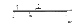
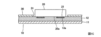
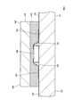
- FIGS. 1A, 1B, and 1C show a mounting structure disclosed in Patent Document 1.
- a microphone 20 as an electronic component is attached to a wiring board (referred to as a substrate with wiring in Patent Literature 1) 10.
- the microphone 20 is a MEMS microphone manufactured using MEMS (Micro Electro Mechanical System) technology.
- the wiring board 10 has a configuration in which an insulating adhesive layer 12 is formed on one surface 11 a of a film 11, and four conductor patterns 13 are formed on the adhesive layer 12.
- the pressure-sensitive adhesive layer 12 is formed on the entire surface 11 a of the film 11.
- a land 13a is formed at one end of each of the four conductor patterns 13, and a land 13b is formed at the other end.
- the microphone 20 is attached to the adhesive layer 12 by pressing the microphone 20 against the adhesive layer 12.
- the terminal 21 of the microphone 20 is in contact with the land 13a of the conductor pattern 13.
- a portion of the bottom surface 20 a of the microphone 20 where the terminal 21 is not formed is adhered to the adhesive layer 12. Therefore, the microphone 20 and the adhesive layer 12 are mechanically connected to each other. Since the elastic restoring force of the pressure-sensitive adhesive layer 12 acts as a load in a direction in which the terminal 21 and the land 13a are pressed against each other, a good and continuous electrical connection between the terminal 21 and the land 13a is obtained.
- Patent Document 1 discloses that a conductor pattern is formed by printing. However, it is not always easy to form a conductor pattern on an adhesive layer, and forming a wiring board is troublesome and costly. This problem is more pronounced when many conductor patterns need to be formed on the pressure-sensitive adhesive layer.
- An object of the present invention is to provide an electronic component mounting technology that can avoid an increase in the cost of a wiring board despite the use of an adhesive.
- the wiring sheet having the adhesive layer is interposed between the electronic component and the wiring board, and the electronic component is indirectly attached to the wiring board.
- the electronic component is directly attached to the adhesive layer of the wiring sheet, and the adhesive layer of the wiring sheet is directly attached to the wiring board. Conduction between the electronic component and the wiring board is achieved stepwise by conduction between the electronic component and the wiring sheet and between the wiring sheet and the wiring board.
- the electronic component is locally attached to the wiring board using the wiring sheet on which the adhesive layer is formed, an increase in the cost of the wiring board can be avoided despite the use of the adhesive.
- FIG. 5 is a partially enlarged cross-sectional view of a conventional mounting structure.
- FIG. 2 is a plan view of the mounting structure according to the first embodiment.
- FIG. 2 is a cross-sectional view of the mounting structure according to the first embodiment.
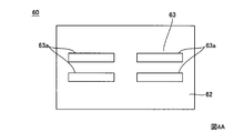
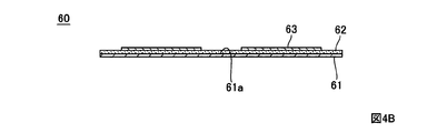
- FIG. The top view of a wiring sheet. Sectional drawing of a wiring sheet.
- the top view of an electronic module Sectional drawing of an electronic module.
- FIG. 9 is a plan view (a part of which is a perspective view) of an attachment structure according to a second embodiment.
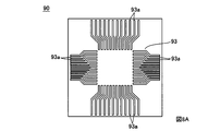
- FIG. The top view of a wiring sheet.
- FIG. 2 is a plan view of the electronic module (a part of which is a perspective view).
- First embodiment> 2A and 2B show a first embodiment of an electronic component mounting structure.
- the electronic module 50 is manufactured, and then the electronic module 50 is attached to the wiring board 40 using an adhesive.
- the electronic module 50 includes a wiring sheet 60 and an electronic component 70 to which the wiring sheet 60 is attached.
- the electronic component 70 has a rectangular parallelepiped shape in this example, and has four terminals 71 on the bottom surface 70a of the electronic component 70 (see FIGS. 3A and 3B).
- the wiring sheet 60 has a configuration in which an insulating pressure-sensitive adhesive layer 62 that can be elastically deformed is formed on one surface 61 a of a base 61, and a conductor pattern 63 is further formed on the pressure-sensitive adhesive layer 62 (see FIGS. 4A and 4B). ).
- the adhesive layer 62 is formed on the entire surface 61 a of the base 61.
- the conductor pattern 63 includes four conductive lines 63a in this embodiment. Two conductive lines 63a are arranged on the right half of the rectangular wiring sheet 60, and the remaining two conductive lines 63a are arranged on the left half. The inner ends of the four conductive wires 63a are portions that directly contact the four terminals 71 of the electronic component 70. The four conductive lines 63a extend in a direction parallel to the long side of the wiring sheet 60. The outer end of each conductive line 63a extends toward the short side of the wiring sheet 60 and is separated from the short side by a predetermined distance.
- the base 61 is a flexible film base material.
- the material of the film substrate include PET (polyethylene terephthalate), PEN (polyethylene naphthalate), and PI (polyimide).
- Examples of the adhesive of the adhesive layer 62 include polyester-based, polyurethane-based, acrylic-based, epoxy-based, phenol-based, silicone-based, polyolefin-based, polyimide-based, vinyl-based, and natural polymer-based polymers.
- the polymer may be a polymer composed of one kind of monomer or a polymer composed of two kinds of monomers.
- a polyester, polyurethane, acrylic, epoxy, phenol, silicone, polyolefin, polyimide, or vinyl monomer or oligomer may be mixed with the polymer. Good.
- the conductor pattern 63 is formed by printing using, for example, a silver paste (silver ink).
- the conductor pattern 63 may be formed by plating.
- FIGS. 5A and 5B show the electronic module 50.
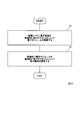
- the electronic component 70 is directly attached to the wiring sheet 60 by pressing the electronic component 70 against the adhesive layer 62 (Step S1).
- the four terminals 71 are in direct contact with the inner ends of the four conductive lines 63a.
- the terminal 71 of the electronic component 70 is electrically connected to the conductor pattern 63 by directly contacting the conductor pattern 63.
- a portion of the bottom surface 70a of the electronic component 70 where the terminal 71 is not formed is mechanically connected to the pressure-sensitive adhesive layer 62 by adhering to the pressure-sensitive adhesive layer 62 (see FIG. 5B). That is, the mechanical connection between the adhesive layer 62 and the electronic component 70 is realized by attaching a part of the surface of the electronic component 70 to a part of the surface of the adhesive layer 62.
- the wiring board 40 is a general wiring board having a conductor pattern formed on the base 41.
- the wiring board 40 is a flexible printed wiring board, and the material of the base 41 is a film base material. 2A and 2B, only a part of the wiring board 40 to which the electronic component 70 is attached is shown, and details of the entire shape and configuration of the wiring board 40 are omitted.
- a conductor pattern 42 including four conductive lines 42a is formed on a part of the wiring board 40 to which the electronic component 70 is attached. The four conductive lines 42a are in direct contact with the four conductive lines 63a of the electronic module 50.
- the mounting structure is manufactured by directly mounting the electronic module on the wiring board (step S2).
- the electronic component 70 of the electronic module 50 is opposed to the surface of the wiring board 40 on which the conductor pattern 42 is formed.
- the four conductive lines 63a of the conductive pattern 63 face the four conductive lines 42a of the conductive pattern 42 of the wiring board 40.
- the electronic module 50 is pressed against the wiring board 40.
- the portion of the wiring sheet 60 located around the electronic component 70 is deformed, and the outer ends of the four conductive lines 63 a of the conductive pattern 63 directly contact the conductive lines 42 a of the conductive pattern 42 of the wiring board 40.
- the wiring sheet 60 is electrically connected to the wiring board 40.
- the upper surface 70 b of the electronic component 70 is in direct contact with the base 41 of the wiring board 40.
- the mechanical connection between the adhesive layer 62 and the wiring board 40 surrounds the electronic component 70.
- the conductor pattern 63 Since the elastic restoring force of the pressure-sensitive adhesive layer 62 acts as a load in a direction in which the conductor pattern 63 and the conductor pattern 42 of the wiring board 40 are pressed against each other, the conductor pattern 63 is satisfactorily electrically connected to the conductor pattern 42.
- the electronic component can be easily attached to the wiring board.
- the electronic module 50 is manufactured by attaching the electronic component 70 to the adhesive layer 62 of the wiring sheet 60, and then the adhesive layer 62 of the electronic module 50 is locally attached to the attaching portion of the wiring board 40. Attach to Therefore, there is no need to form an adhesive layer on the entire surface of the wiring board, that is, a general wiring board without an adhesive layer can be used. Therefore, an increase in the cost of the wiring board can be avoided.
- An electronic module including electronic components can be manufactured as a module common to various types of wiring boards or as a general-purpose module. Therefore, improvement in production efficiency can be expected.
- the mounting structure of this embodiment is sandwiched between a wiring board and a wiring sheet that are adhered to each other.
- a structure in which an electronic component is covered by a wiring board and a wiring sheet more specifically, an electronic component is inside a closed space formed by a closed loop-shaped adhesive portion between the adhesive layer and the wiring board. Since the structure is located, the electronic component is not exposed to the outside. That is, the waterproofness of the electronic component is guaranteed.
- the adhesive area between the electronic component 20 and the adhesive layer 12 is small. If the wiring board 10 is bent so that the surface on which the electronic component is attached is outside, there is a possibility that the terminal 21 of the electronic component 20 separates from the conductor pattern 13 or the electronic component 20 falls off. was there.
- the electronic component 70 is sandwiched between the wiring sheet 60 and the wiring board 40, and the adhesive area between the adhesive layer 62 of the wiring sheet 60 and the wiring board 40 is greatly increased. Occurrence of troubles can be prevented. Therefore, a highly reliable mounting structure that is resistant to bending is realized.
- the conductor pattern of the wiring sheet plays a role of relaying the terminal of the electronic component and the conductor pattern of the wiring board.
- the two conductive lines 63a of the conductor pattern 63 extend in parallel at a constant arrangement interval on the right side of the electronic component 70, and the remaining two conductive lines 63a of the conductor pattern 63 Are extended in parallel at a constant arrangement interval on the left side of the (see FIG. 4A).
- the conductor pattern of the wiring sheet includes two or more conductive lines whose intervals change in the extending direction of two adjacent conductive lines.
- FIG. 6 shows an electronic component mounting structure according to the second embodiment. In each drawing, only a portion of the wiring board 110 on which the electronic component 80 is mounted is illustrated.
- the electronic component 80 is a microcomputer chip that can be attached to a surface such as a substrate. Twelve terminals 81 are arranged on each of four sides of the square bottom surface 80a of the electronic component 80 (see FIGS. 7A and 7B).
- the adhesive layer 92 is formed on the entire surface 91a of the base 91 of the wiring sheet 90 (see FIG. 8B).
- a conductive pattern 93 is formed on the adhesive layer 92. Since the conductor pattern 93 is very thin compared to the base 91 and the adhesive layer 92, the illustration of the conductor pattern 93 is omitted in FIG. 8B.
- Conductive pattern 93 includes 48 conductive lines 93a. Twelve conductive lines 93 a extend from each of the four sides of the rectangular wiring sheet 90 toward the center of the wiring sheet 90. The inner ends of the forty-eight conductive lines 93a directly contact the forty-eight terminals 81 of the electronic component 80.
- the outer ends of the 48 conductive lines 93a are separated from the edge of the wiring sheet 90 by a predetermined distance.
- the constituent materials of the base 91 and the adhesive layer 92 are the same as the constituent materials of the base 61 and the adhesive layer 62 in the first embodiment, respectively.
- the interval between two adjacent conductive lines 93a changes in the extending direction of the two adjacent conductive lines 93a (see FIG. 8A).
- the interval at the inner end of two adjacent conductive lines 93a is smaller than the interval at the outer end, and similarly, the interval extending from the lower side of the wiring sheet 90
- the interval at the inner end of two adjacent conductive lines 93a is smaller than the interval at the outer end.
- the interval between the inner ends of the two adjacent conductive lines 93a is wider than the interval at the outer end, and similarly, the 12 extending from the left side of the wiring sheet 90.
- the interval at the inner end of two adjacent conductive lines 93a is wider than the interval at the outer end.
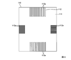
- the wiring board 110 is a flexible printed wiring board, like the wiring board 40 in the first embodiment.
- a predetermined conductor pattern 112 is formed on the base 111.
- the conductor pattern 112 includes 48 conductive lines 112a.
- the 48 conductive lines 112a of the conductive pattern 112 directly contact the 48 conductive lines 93a of the conductive pattern 93.
- the wiring board 40 and the wiring board 110 are flexible printed wiring boards, and the material of the base 41 and the base 111 is a flexible film base material.
- the material of the base 41 and the base 111 may be a rigid base material having no flexibility.
- one or both of the base material of the wiring board and the base material of the wiring sheet is a rigid base material. Is also good.
- FIG. 11 shows a mounting structure of an electronic component 150 in which the base 121 of the wiring board 120 and the base 141 of the wiring sheet 140 of the electronic module 130 are rigid base materials as the third embodiment.
- the mounting structure of the electronic component shown in FIG. 11 can be realized even if the base 121 and the base 141 are rigid.
- reference numeral 143 indicates a conductor pattern of the wiring sheet 140
- reference numeral 122 indicates a conductor pattern of the wiring board 120
- reference numeral 151 indicates a terminal of the electronic component 150.
- the conductor pattern 122 of the wiring board 120 is in direct contact with the conductor pattern 143. Not only that, but also the terminal 151 facing the wiring board 120 may be directly contacted. That is, in the case of mounting an electronic component of a type having terminals extending on both sides, a mounting structure in which the terminals of the electronic component are sandwiched between the conductor pattern of the wiring board and the conductor pattern of the wiring sheet can be implemented. It goes without saying that such an attachment structure can be implemented regardless of the flexibility of the material of the base of the wiring board or the material of the base of the wiring sheet.
- ordinal numbers for example, the prefix “No.” combined with a Chinese number or an arithmetic digit “No. It is not intended to limit the elements that are modified with or associated with the ordinal by the order of the elements or the amount of the elements. Unless otherwise specified, the use of ordinal numbers is simply used as a convenient way of distinguishing two or more elements from each other. Therefore, for example, the phrase “first X” and the phrase “second X” are expressions for distinguishing two Xs, and do not necessarily mean that the total number of Xs is 2, or It does not necessarily mean that the first X must precede the second X.
- the term "comprises” and its conjugations are used as non-exclusive expressions.
- the sentence "X includes A and B” does not deny that X includes a component other than A and B (for example, C).
- the sentence when a sentence includes a term “comprising” or a word in which the inflection thereof is combined with a negative word, the sentence only refers to the object.
- the sentence "X does not include A and B” acknowledges that X may include components other than A and B.
- the term “or” as used in the description or in the claims is not intended to be an exclusive or.
- the present disclosure when an article or a part of speech similar to an article is added by translation, for example, "a”, “an”, and “the” in English, the present disclosure indicates that a plurality of nouns It may include being a shape.
Landscapes
- Engineering & Computer Science (AREA)
- Microelectronics & Electronic Packaging (AREA)
- Manufacturing & Machinery (AREA)
- Structure Of Printed Boards (AREA)
- Electric Connection Of Electric Components To Printed Circuits (AREA)
- Combinations Of Printed Boards (AREA)
- Wire Bonding (AREA)
- Physics & Mathematics (AREA)
- Geometry (AREA)
- Structures For Mounting Electric Components On Printed Circuit Boards (AREA)
Abstract
電子部品が配線板に取り付けられた取付構造において、電子部品と配線板との間に粘着剤層を持つ配線シートが介在しており、電子部品は配線板に間接的に取り付けられる。電子部品は配線シートの粘着剤層に直接的に取り付けられており、配線シートの粘着剤層は配線板に直接的に取り付けられている。電子部品は配線板との間の導通は、電子部品と配線シートとの導通および配線シートと配線板との導通によって達成される。
Description
本発明は、配線板に電子部品を取り付ける電子部品取付技術に関する。
熱(例えば半田)を用いることなく配線板に電子部品を取り付ける方法の1例として粘着剤を用いる方法が知られている。特許文献1は、粘着剤を用いる取付構造を開示している。
図1A,1B,1Cは、特許文献1に開示されている取付構造を示している。この例では、配線板(特許文献1では配線付き基材と称している)10に電子部品としてのマイクロホン20が取り付けられている。マイクロホン20はMEMS(Micro Electro Mechanical System)技術を用いて製造されるMEMSマイクロホンである。
配線板10は、フィルム11の一面11a上に絶縁性粘着剤層12が形成され、さらに粘着剤層12上に4個の導体パターン13が形成された構成を持つ。粘着剤層12は、フィルム11の一面11aの全面に形成されている。4個の導体パターン13のそれぞれの一端にランド13aが形成されており、それぞれの他端にランド13bが形成されている。
マイクロホン20を粘着剤層12に押し付けることによって、マイクロホン20は粘着剤層12に取り付けられている。この状態において、マイクロホン20の端子21は、導体パターン13のランド13aに接触している。マイクロホン20の底面20aにおいて端子21が形成されていない部分は、粘着剤層12に粘着している。したがって、マイクロホン20と粘着剤層12は互いに機械的に結合している。粘着剤層12の弾性復元力が端子21とランド13aとを互いに圧接させる向きの荷重として働くので、端子21とランド13aとの良好で継続的な電気的接続状態が得られる。
導体パターン13が形成されている配線板10の面は、マイクロホン20が位置する部位及び4個のランド13bが位置する部位を除いて、カバーフィルム30によって覆われている。換言すれば、窓31及び切欠き32がカバーフィルム30に形成されている。
特許文献1は、導体パターンを印刷によって形成することを開示している。しかし、粘着剤層上に導体パターンを形成することは必ずしも容易でなく、配線板の形成は面倒でコストがかかる。粘着剤層上に多くの導体パターンを形成する必要がある場合、この問題はもっと顕著である。
本発明の目的は、粘着剤の使用にもかかわらず配線板のコストの増大を回避できる電子部品取付技術を提供することである。
ここで述べる技術事項は、請求の範囲に記載された発明を明示的にまたは黙示的に限定するためではなく、さらに、本発明によって利益を受ける者(例えば出願人と権利者である)以外の者によるそのような限定を容認する可能性の表明でもなく、単に、本発明の要点を容易に理解するために記載される。
本発明によると、電子部品と配線板との間に粘着剤層を持つ配線シートが介在しており、電子部品は配線板に間接的に取り付けられる。電子部品は配線シートの粘着剤層に直接的に取り付けられており、配線シートの粘着剤層は配線板に直接的に取り付けられている。電子部品は配線板との間の導通は、電子部品と配線シートとの導通および配線シートと配線板との導通によって段階的に達成される。
本発明によると、電子部品と配線板との間に粘着剤層を持つ配線シートが介在しており、電子部品は配線板に間接的に取り付けられる。電子部品は配線シートの粘着剤層に直接的に取り付けられており、配線シートの粘着剤層は配線板に直接的に取り付けられている。電子部品は配線板との間の導通は、電子部品と配線シートとの導通および配線シートと配線板との導通によって段階的に達成される。
本発明によると、粘着剤層が形成された配線シートを用いて電子部品を配線板に局所的に取り付けるので、粘着剤の使用にもかかわらず配線板のコストの増大を回避できる。
本発明の実施形態を、図面を参照して説明する。
<第1実施形態>
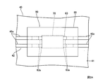
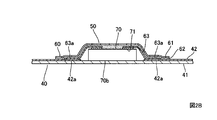
図2A,2Bは、電子部品の取付構造の第1実施形態を示している。この実施形態では、先ず、電子モジュール50を作製し、次いで、粘着剤を用いて電子モジュール50を配線板40に取り付ける。
図2A,2Bは、電子部品の取付構造の第1実施形態を示している。この実施形態では、先ず、電子モジュール50を作製し、次いで、粘着剤を用いて電子モジュール50を配線板40に取り付ける。
電子モジュール50は、配線シート60と、配線シート60が取り付けられた電子部品70を含む。電子部品70は、この例では直方体状の形状を有しており、電子部品70の底面70aに4個の端子71を持つ(図3A,3B参照)。
配線シート60は、基部61の一面61a上に弾性変形可能な絶縁性粘着剤層62が形成され、さらに粘着剤層62の上に導体パターン63が形成された構成を有する(図4A,4B参照)。粘着剤層62は、基部61の一面61aの全面に形成されている。
導体パターン63は、この実施形態では、4個の導電線63aを含む。長方形形状の配線シート60の右半分に2個の導電線63aが配置されており、左半分に残りの2個の導電線63aが配置されている。4個の導電線63aの内端は、電子部品70の4個の端子71と直接的に接触する部位である。4個の導電線63aは、配線シート60の長辺と平行な方向に伸びている。各導電線63aの外端は、配線シート60の短辺に向かって伸びており、短辺から所定距離だけ離れている。
配線シート60において、基部61は可撓性を有するフィルム基材である。フィルム基材の材料として、PET(ポリエチレンテレフタレート)、PEN(ポリエチレンナフタレート)、PI(ポリイミド)等を例示できる。
粘着剤層62の粘着剤として、ポリエステル系、ポリウレタン系、アクリル系、エポキシ系、フェノール系、シリコーン系、ポリオレフィン系、ポリイミド系、ビニル系、天然高分子系のポリマーなどを例示できる。ポリマーは、1種類のモノマーで構成されるポリマーであってもよいし、2種類のモノマーで構成されるポリマーであってもよい。
粘着性または機械的特性を向上させるために、ポリマーに、例えばポリエステル系、ポリウレタン系、アクリル系、エポキシ系、フェノール系、シリコーン系、ポリオレフィン系、ポリイミド系、ビニル系のモノマーあるいはオリゴマーを混ぜてもよい。
導体パターン63は、例えば銀ペースト(銀インク)を用いた印刷によって形成される。めっきによって導体パターン63を形成してもよい。
図5A、5Bは、電子モジュール50を示している。電子部品70は、電子部品70を粘着剤層62に押し付けることによって、配線シート60に直接的に取り付けられる(ステップS1)。4個の端子71は、4個の導電線63aの内端と直接的に接触している。
電子部品70の端子71は、導体パターン63に直接的に接触することによって導体パターン63と電気的に接続している。電子部品70の底面70aにおいて端子71が形成されていない部分は、粘着剤層62に粘着することによって、粘着剤層62と機械的に結合している(図5B参照)。つまり、粘着剤層62と電子部品70との間の機械的結合は、電子部品70の表面の一部が、粘着剤層62の表面の一部に貼り付けられることによって実現する。
粘着剤層62の弾性復元力が電子部品70の端子71と導体パターン63とを互いに圧接させる向きの荷重として働くので、端子71は導体パターン63に良好に電気的に接続される。
この実施形態では、電子モジュール50を配線板40に取り付けることによって、配線板40に電子部品70が取り付けられた電子部品の取付構造を生産する。
配線板40は、基部41の上に導体パターンが形成された一般的な配線板である。この実施形態では、配線板40はフレキシブルプリント配線板であり、基部41の材質はフィルム基材である。図2A,2Bでは、電子部品70が取り付けられる配線板40の一部分だけが示されており、配線板40の全体の形状および構成の詳細は省略されている。電子部品70が取り付けられる配線板40の一部分に、4個の導電線42aを含む導体パターン42が形成されている。4個の導電線42aは、電子モジュール50の4個の導電線63aと直接的に接触する。
配線板40への電子モジュール50の取り付けは、以下のように行われる。
配線板に電子モジュールを直接的に取り付けることによって取付構造を製造する(ステップS2)。導体パターン42が形成されている配線板40の面に、電子モジュール50の電子部品70を対向させる。導体パターン63の4個の導電線63aを配線板40の導体パターン42の4個の導電線42aに対面させる。電子モジュール50の全体を押圧することによって、電子モジュール50を配線板40に押し付ける。電子部品70の周りに位置する配線シート60の部位が変形し、導体パターン63の4個の導電線63aの外端は配線板40の導体パターン42の導電線42aに直接的に接触する。この結果、配線シート60は配線板40に電気的に接続する。電子部品70の上面70bは、配線板40の基部41に直接的に接触している。
配線シート60の変形によって配線板40の板面に直接的に接触した粘着剤層62は配線板40に粘着し、粘着剤層62と配線板40は互いに機械的に結合される。つまり、粘着剤層62と配線板40との間の機械的結合は、粘着剤層62の一部(具体的には、導体パターン63が形成されておらず且つ電子部品70が貼り付けられていない表面の少なくとも一部)が、配線板40における導体パターン42の表面と導体パターン42が形成されていない基部41の表面とのうちの少なくとも一方の一部に貼り付けられることによって実現する。粘着剤層62と配線板40との機械的結合部分は、電子部品70の周りを囲んでいる。
粘着剤層62の弾性復元力が導体パターン63と配線板40の導体パターン42とを互いに圧接させる向きの荷重として働くので、導体パターン63は導体パターン42に良好に電気的に接続される。
電子部品の取付構造の第1実施形態を取付構造の生産方法と共に説明したが、第1実施形態によれば下記の効果が得られる。
(1)粘着剤を用いているので、電子部品を配線板に簡単に取り付けることができる。この実施形態では、先ず、配線シート60の粘着剤層62に電子部品70を取り付けることによって電子モジュール50を作製し、次いで、電子モジュール50の粘着剤層62を配線板40の取付部位に局所的に取り付ける。したがって、配線板の全面に粘着剤層を形成する必要が無く、つまり粘着剤層の無い一般的な配線板を用いることができる。それ故、配線板のコストの増大を避けることができる。
(2)電子部品を含む電子モジュールを、さまざまなタイプの配線板に共通のモジュールとして、或いは、汎用モジュールとして作製できる。したがって、生産効率の向上を期待できる。
(3)この実施形態の取付構造は、互いに粘着している配線板と配線シートとに挟まれている。特に、配線板と配線シートとによって電子部品が覆われた構造、もっと具体的には、粘着剤層と配線板との間の閉ループ状の粘着部によって形成された閉空間の内部に電子部品が位置する構造であるから、電子部品が外部に露出しない。つまり、電子部品の防水性が保証される。
(4)従来の取付構造(図1A~1C参照)によると、電子部品20と粘着剤層12との粘着面積が少ない。電子部品が取り付けられた面が外側となるように配線板10に曲げが加わると、電子部品20の端子21が導体パターン13から乖離する不具合、或いは、電子部品20が脱落する不具合が生じる可能性があった。しかし、この実施形態では、電子部品70は配線シート60と配線板40とによって挟み込まれており、且つ配線シート60の粘着剤層62と配線板40の粘着面積も大幅に増大するので、そのような不具合の発生を防止できる。したがって、曲げに強く且つ信頼性の高い取付構造が実現する。
<第2実施形態>
配線シートの導体パターンは電子部品の端子と配線板の導体パターンとを中継する役割を果たす。第1実施形態では、導体パターン63の2個の導電線63aは電子部品70の右側で一定の配列間隔で平行に伸びており、導体パターン63の残りの2個の導電線63aは電子部品70の左側で一定の配列間隔で平行に伸びている(図4A参照)。しかし、第2実施形態では、配線シートの導体パターンは、隣り合う2個の導電線の伸長方向でその間隔が変化する2個以上の導電線を含む。図6は、第2実施形態の電子部品の取付構造を示している。各図では、電子部品80が実装される配線板110の部分のみが図示されている。
配線シートの導体パターンは電子部品の端子と配線板の導体パターンとを中継する役割を果たす。第1実施形態では、導体パターン63の2個の導電線63aは電子部品70の右側で一定の配列間隔で平行に伸びており、導体パターン63の残りの2個の導電線63aは電子部品70の左側で一定の配列間隔で平行に伸びている(図4A参照)。しかし、第2実施形態では、配線シートの導体パターンは、隣り合う2個の導電線の伸長方向でその間隔が変化する2個以上の導電線を含む。図6は、第2実施形態の電子部品の取付構造を示している。各図では、電子部品80が実装される配線板110の部分のみが図示されている。
電子部品80は、基板などの表面に取り付けることのできるマイクロコンピュータチップである。電子部品80の方形状底面80aの4辺のそれぞれに12個の端子81が配列している(図7A,7B参照)。
配線シート60と同様、配線シート90の基部91の一面91aの全部に粘着剤層92が形成されている(図8B参照)。粘着剤層92の上に導体パターン93が形成されている。導体パターン93は、基部91と粘着剤層92に比べて非常に薄いので、図8Bにおいて、導体パターン93の図示が省略されている。導体パターン93は、48個の導電線93aを含む。方形状配線シート90の4辺のそれぞれから12個の導電線93aが配線シート90の中央に向かって伸びている。48個の導電線93aの内端は、電子部品80の48個の端子81と直接的に接触する。48個の導電線93aの外端は、配線シート90の端縁から所定距離だけ離れている。基部91及び粘着剤層92の構成材料はそれぞれ、第1実施形態における基部61及び粘着剤層62の構成材料と同じである。
48個の導電線93aに関して、隣り合う2個の導電線93aの間隔は、隣り合う2個の導電線93aの伸長方向において変化する(図8A参照)。配線シート90の上辺から伸びる12個の導電線93aに関して、隣り合う2個の導電線93aの内端での間隔は、外端での間隔より狭く、同様に、配線シート90の下辺から伸びる12個の導電線93aに関して、隣り合う2個の導電線93aの内端での間隔は、外端での間隔より狭い。配線シート90の右辺から伸びる12個の導電線93aに関して、隣り合う2個の導電線93aの内端での間隔は、外端での間隔より広く、同様に、配線シート90の左辺から伸びる12個の導電線93aに関して、隣り合う2個の導電線93aの内端での間隔は、外端での間隔より広い。
配線シート90に電子部品80が取り付けられることによって、図9に示す電子モジュール100が作製される。
配線板110は、第1実施形態における配線板40と同様、フレキシブルプリント配線板である。基部111の上に所定の導体パターン112が形成されている。導体パターン112は48個の導電線112aを含む。導体パターン112の48個の導電線112aは、導体パターン93の48個の導電線93aと直接的に接触する。
配線板110に電子モジュール100を取り付けることによって、配線板110に電子部品80が取り付けられた電子部品の取付構造を生産する。粘着剤層92と電子部品80との機械的結合及び粘着剤層92と配線板110との機械的結合は第1実施形態のそれらと同じである。
<第3実施形態>
第1実施形態及び第2実施形態では配線板40及び配線板110はフレキシブルプリント配線板であり、基部41及び基部111の材質は可撓性を有するフィルム基材である。しかし、基部41及び基部111の材質は可撓性の無いリジッド基材でもよい。
第1実施形態及び第2実施形態では配線板40及び配線板110はフレキシブルプリント配線板であり、基部41及び基部111の材質は可撓性を有するフィルム基材である。しかし、基部41及び基部111の材質は可撓性の無いリジッド基材でもよい。
粘着剤層の厚み等の条件が十分であり、且つ、粘着による機械的結合が達成されるならば、配線板の基部と配線シートの基部の何れか又は両方の材質はリジッド基材であってもよい。
図11は、第3実施形態として、配線板120の基部121及び電子モジュール130の配線シート140の基部141の各材質がリジッド基材である電子部品150の取付構造を示している。
例えば、十分に小さく薄いチップ抵抗である電子部品150と比較して厚い粘着剤層142を形成すれば、基部121及び基部141がリジッドであっても図11に示す電子部品の取付構造を実現できる。図11中、符号143は配線シート140の導体パターンを示し、符号122は配線板120の導体パターンを示し、符号151は電子部品150の端子を示す。
<第4実施形態>
図示を省略するが、基部141に向く底面から配線板120に向く面に伸びる端子151が形成されている電子部品150の場合、配線板120の導体パターン122は、導体パターン143と直接的に接触するだけでなく、配線板120に向く端子151の部分にも直接に接触してもよい。つまり、表裏両面に伸びる端子を持つタイプの電子部品の取り付けの場合、配線板の導体パターンと配線シートの導体パターンとによって電子部品の端子を挟む取付構造も実施できる。このような取付構造が、配線板の基部の材質または配線シートの基部の材質の可撓性の有無にかかわらず実施できることは、言うまでもない。
図示を省略するが、基部141に向く底面から配線板120に向く面に伸びる端子151が形成されている電子部品150の場合、配線板120の導体パターン122は、導体パターン143と直接的に接触するだけでなく、配線板120に向く端子151の部分にも直接に接触してもよい。つまり、表裏両面に伸びる端子を持つタイプの電子部品の取り付けの場合、配線板の導体パターンと配線シートの導体パターンとによって電子部品の端子を挟む取付構造も実施できる。このような取付構造が、配線板の基部の材質または配線シートの基部の材質の可撓性の有無にかかわらず実施できることは、言うまでもない。
明細書と請求の範囲では、序数詞(例えば、接頭辞「第」に漢数詞または算用数字を組み合わせた「第○」)は、特段の断りが無い限り、序数詞の定義にもかかわらず、序数詞で修飾されるまたは序数詞と結合する要素を当該要素の順序または当該要素の量で限定することを意図しない。序数詞の使用は、特段の断りが無い限り、単に、2つ以上の要素を互いに区別する便利な表現方法として使用される。したがって、例えば語句「第1のX」と語句「第2のX」は、2つのXを区別するための表現であり、Xの総数が2であることを意味するものでは必ずしもなく、あるいは、第1のXが第2のXに先行しなければならないことを意味するものでは必ずしもない。
明細書と請求の範囲では、用語「含む」とその語形変化は非排他的表現として使用されている。例えば、「XはAとBを含む」という文は、XがAとB以外の構成要素(例えばC)を含むことを否定しない。また、明細書と請求の範囲において或る文が用語「含む」またはその語形変化が否定辞と結合した語句を含む場合、当該文は目的語について言及するだけである。したがって、例えば「XはAとBを含まない」という文は、XがAとB以外の構成要素を含む可能性を認めている。さらに、明細書あるいは請求の範囲において使用されている用語「または」は排他的論理和ではないことが意図される。
本開示において、例えば、英語での“a”,“an”及び“the”のように、翻訳によって冠詞または冠詞に類する品詞が追加された場合、本開示は、当該品詞の後に続く名詞が複数形であることを含んでもよい。
以上、本発明の実施形態について説明したが、本発明はこれらの実施形態に限定されるものではない。本発明の要旨を逸脱しない範囲において種々の変更と変形が許される。選択され且つ説明された実施形態は、本発明の原理およびその実際的応用を解説するためのものである。本発明は様々な変更あるいは変形を伴って様々な実施形態として使用され、様々な変更あるいは変形は期待される用途に応じて決定される。そのような変更および変形のすべては、添付の請求の範囲によって規定される本発明の範囲に含まれることが意図されており、公平、適法および公正に与えられる広さに従って解釈される場合、同じ保護が与えられることが意図されている。
Claims (12)
- 電子部品の取付構造を製造する方法であって、ただし、上記取付構造は、上記電子部品と、配線板と、を含んでおり、上記電子部品は端子を含んでおり、上記配線板は、第1基部と、上記第1基部の上に形成されている第1導体パターンと、を含んでおり、上記取付構造において上記電子部品は上記配線板に間接的に取り付けられており、
配線シートに上記電子部品を直接的に取り付けることによって電子モジュールを製造する第1ステップと、ただし、上記配線シートは、第2基部と、上記第2基部の上に形成されている絶縁性の粘着剤層と、上記粘着剤層の上に形成されている第2導体パターンと、を含んでおり、上記電子モジュールにおいて、上記電子部品の上記端子は上記第2導体パターンと接触しており、且つ、上記端子が形成されている部分を除く上記電子部品の表面の少なくとも一部は、上記第2導体パターンが形成されている部分を除く上記粘着剤層の表面の少なくとも一部に粘着しており、
上記配線板に上記電子モジュールを直接的に取り付けることによって上記取付構造を製造する第2ステップと、ただし、上記取付構造において、上記第2導体パターンは上記第1導体パターンと接触しており、且つ、上記電子モジュールにおいて露出している上記粘着剤層の表面の少なくとも一部は、上記配線板の表面の少なくとも一部に粘着しており、
を有する。 - 請求項1に記載の方法において、
上記第1基部と上記第2基部の一方または両方の材質は、可撓性を有するフィルム基材である。 - 請求項1または請求項2に記載の方法において、
上記第2導体パターンは、複数の導電線を含み、
上記複数の導電線のうち隣り合う2個の導電線の間隔は、当該隣り合う2個の導電線の伸長方向において変化している。 - 電子部品の取付構造であって、
上記電子部品と、ただし、上記電子部品は端子を含んでおり、
配線板と、ただし、上記配線板は、第1基部と、上記第1基部の上に形成されている第1導体パターンと、を含んでおり、
配線シートと、ただし、上記配線シートは、第2基部と、上記第2基部の上に形成されている絶縁性の粘着剤層と、上記粘着剤層の上に形成されている第2導体パターンと、を含んでおり、
を含み、
上記電子部品の上記端子は上記第2導体パターンと接触しており、
上記端子が形成されている部分を除く上記電子部品の表面の少なくとも一部は、上記第2導体パターンが形成されている部分を除く上記粘着剤層の表面の少なくとも一部に粘着しており、
上記第2導体パターンは上記第1導体パターンと接触しており、
上記第2導体パターンが形成されている部分および上記電子部品と粘着している部分を除く上記粘着剤層の表面の少なくとも一部は、上記配線板の表面の少なくとも一部に粘着している。 - 請求項4に記載の構造において、
上記第1基部と上記第2基部の一方または両方の材質は、可撓性を有するフィルム基材である。 - 請求項4または請求項5に記載の構造において、
上記第2導体パターンは、複数の導電線を含み、
上記複数の導電線のうち隣り合う2個の導電線の間隔は、当該隣り合う2個の導電線の伸長方向において変化している。 - 請求項4から請求項6のいずれかに記載の構造において、
上記電子部品は、互いに粘着している上記配線シートと上記配線板とに挟まれている。 - 電子モジュールであって、
電子部品と、ただし、上記電子部品は端子を含んでおり、
配線シートと、ただし、上記配線シートは、基部と、上記基部の上に形成されている絶縁性の粘着剤層と、上記粘着剤層の上に形成されている導体パターンと、を含んでおり、
を含み、
上記電子部品の上記端子は上記導体パターンと接触しており、
上記端子が形成されている部分を除く上記電子部品の表面の少なくとも一部は、上記導体パターンが形成されている部分を除く上記粘着剤層の表面の少なくとも一部に粘着している。 - 請求項8に記載の電子モジュールにおいて、
上記基部の材質は、可撓性を有するフィルム基材である。 - 請求項8または請求項9に記載の電子モジュールにおいて、
上記導体パターンは、複数の導電線を含み、
上記複数の導電線のうち隣り合う2個の導電線の間隔は、当該隣り合う2個の導電線の伸長方向において変化している。 - 配線シートであって、
基部と、
上記基部の上に形成されている絶縁性の粘着剤層と、
上記粘着剤層の上に形成されている導体パターンと、
を含み、
上記導体パターンは、複数の導電線を含み、
上記複数の導電線のうち隣り合う2個の導電線の間隔は、当該隣り合う2個の導電線の伸長方向において変化している。 - 請求項11に記載の配線シートにおいて、
上記基部の材質は、可撓性を有するフィルム基材である。
Priority Applications (2)
| Application Number | Priority Date | Filing Date | Title |
|---|---|---|---|
| CN201980054813.XA CN112586097B (zh) | 2018-10-04 | 2019-08-30 | 电子部件的安装结构的制造方法 |
| US17/267,887 US11881470B2 (en) | 2018-10-04 | 2019-08-30 | Method for manufacturing mounting structure for electronic component, mounting structure for electronic component, electronic module, and wiring sheet |
Applications Claiming Priority (2)
| Application Number | Priority Date | Filing Date | Title |
|---|---|---|---|
| JP2018188844A JP6663965B1 (ja) | 2018-10-04 | 2018-10-04 | 電子部品の実装構造を生産する方法、電子部品の実装構造、電子部品実装用モジュール及び電子部品実装用配線板 |
| JP2018-188844 | 2018-10-04 |
Publications (1)
| Publication Number | Publication Date |
|---|---|
| WO2020071027A1 true WO2020071027A1 (ja) | 2020-04-09 |
Family
ID=70000466
Family Applications (1)
| Application Number | Title | Priority Date | Filing Date |
|---|---|---|---|
| PCT/JP2019/034178 Ceased WO2020071027A1 (ja) | 2018-10-04 | 2019-08-30 | 電子部品の取付構造の製造方法、電子部品の取付構造、電子モジュール、配線シート |
Country Status (5)
| Country | Link |
|---|---|
| US (1) | US11881470B2 (ja) |
| JP (1) | JP6663965B1 (ja) |
| CN (1) | CN112586097B (ja) |
| TW (1) | TWI802759B (ja) |
| WO (1) | WO2020071027A1 (ja) |
Citations (6)
| Publication number | Priority date | Publication date | Assignee | Title |
|---|---|---|---|---|
| JP2005252134A (ja) * | 2004-03-08 | 2005-09-15 | Casio Comput Co Ltd | フィルム基板の接合方法およびフィルム基板の接合構造 |
| JP2008122523A (ja) * | 2006-11-09 | 2008-05-29 | Toshiba Matsushita Display Technology Co Ltd | 液晶表示装置 |
| JP2010251706A (ja) * | 2009-03-25 | 2010-11-04 | Panasonic Corp | 装着用発電モジュール |
| WO2017043480A1 (ja) * | 2015-09-09 | 2017-03-16 | 株式会社ソシオネクスト | 半導体パッケージ |
| US9814142B1 (en) * | 2015-06-24 | 2017-11-07 | Automated Assembly Corporation | Electronic devices wire bonded to substrate through an adhesive layer and method of making the same |
| JP6293938B1 (ja) * | 2017-02-08 | 2018-03-14 | 日本航空電子工業株式会社 | フィルム面受音型音センサモジュール |
Family Cites Families (8)
| Publication number | Priority date | Publication date | Assignee | Title |
|---|---|---|---|---|
| JP2004086852A (ja) * | 2002-03-18 | 2004-03-18 | Toray Eng Co Ltd | 非接触idカード類及びその製造方法 |
| KR100510486B1 (ko) * | 2002-04-08 | 2005-08-26 | 삼성전자주식회사 | 양면 반도체 칩을 위한 반도체 패키지 및 그 제조방법 |
| CN1228825C (zh) * | 2003-01-30 | 2005-11-23 | 矽品精密工业股份有限公司 | 半导体芯片封装结构及其制造方法 |
| JP2004281538A (ja) * | 2003-03-13 | 2004-10-07 | Seiko Epson Corp | 電子装置及びその製造方法、回路基板並びに電子機器 |
| CN1601936A (zh) | 2003-09-22 | 2005-03-30 | 捷耀光通讯股份有限公司 | 使用芯片直接封装(COB)制程的双向光收发模组(Bi-Di TRx) |
| JP5605429B2 (ja) * | 2010-04-08 | 2014-10-15 | 日本電気株式会社 | 半導体素子内蔵配線基板 |
| JP5540276B2 (ja) * | 2011-03-31 | 2014-07-02 | Tdk株式会社 | 電子部品内蔵基板及びその製造方法 |
| JP6199471B1 (ja) | 2016-10-31 | 2017-09-20 | 日本航空電子工業株式会社 | コネクタ組立体 |
-
2018
- 2018-10-04 JP JP2018188844A patent/JP6663965B1/ja active Active
-
2019
- 2019-08-30 WO PCT/JP2019/034178 patent/WO2020071027A1/ja not_active Ceased
- 2019-08-30 CN CN201980054813.XA patent/CN112586097B/zh active Active
- 2019-08-30 US US17/267,887 patent/US11881470B2/en active Active
- 2019-10-03 TW TW108135799A patent/TWI802759B/zh active
Patent Citations (6)
| Publication number | Priority date | Publication date | Assignee | Title |
|---|---|---|---|---|
| JP2005252134A (ja) * | 2004-03-08 | 2005-09-15 | Casio Comput Co Ltd | フィルム基板の接合方法およびフィルム基板の接合構造 |
| JP2008122523A (ja) * | 2006-11-09 | 2008-05-29 | Toshiba Matsushita Display Technology Co Ltd | 液晶表示装置 |
| JP2010251706A (ja) * | 2009-03-25 | 2010-11-04 | Panasonic Corp | 装着用発電モジュール |
| US9814142B1 (en) * | 2015-06-24 | 2017-11-07 | Automated Assembly Corporation | Electronic devices wire bonded to substrate through an adhesive layer and method of making the same |
| WO2017043480A1 (ja) * | 2015-09-09 | 2017-03-16 | 株式会社ソシオネクスト | 半導体パッケージ |
| JP6293938B1 (ja) * | 2017-02-08 | 2018-03-14 | 日本航空電子工業株式会社 | フィルム面受音型音センサモジュール |
Also Published As
| Publication number | Publication date |
|---|---|
| JP2020057729A (ja) | 2020-04-09 |
| CN112586097B (zh) | 2024-07-12 |
| CN112586097A (zh) | 2021-03-30 |
| TW202017392A (zh) | 2020-05-01 |
| US11881470B2 (en) | 2024-01-23 |
| TWI802759B (zh) | 2023-05-21 |
| JP6663965B1 (ja) | 2020-03-13 |
| US20210193612A1 (en) | 2021-06-24 |
Similar Documents
| Publication | Publication Date | Title |
|---|---|---|
| US20160211473A1 (en) | Electrically interconnecting foil | |
| KR20180010890A (ko) | 연성 회로기판, cof 모듈 및 이를 포함하는 전자 디바이스 | |
| US10219379B1 (en) | Stacked flexible printed circuit board assembly with side connection section | |
| CN110720258B (zh) | 柔性布线电路基板及成像装置 | |
| CN106973499A (zh) | 一种包括印刷电路板和柔性电路板的模组及其制造方法 | |
| CN105992460A (zh) | 刚挠结合板及其制作方法 | |
| CN107251659A (zh) | 柔性基板、带柔性基板的部件以及带柔性基板的部件的制造方法 | |
| TWI802759B (zh) | 電子零件的安裝構造的製造方法、電子零件的安裝構造、電子模組、配線片 | |
| CN102131340A (zh) | 挠性印刷配线板、挠性印刷配线板的制造方法、具有挠性印刷配线板的电子设备 | |
| US10559437B1 (en) | Membrane switch device and keyboard device | |
| KR101759713B1 (ko) | 전기접촉단자 | |
| CN110730998B (zh) | 开关 | |
| CN112447688A (zh) | 发光装置以及发光装置的制造方法 | |
| US20160146436A1 (en) | Led unit and led module having the same | |
| WO2019077990A1 (ja) | 基板積層体、および、撮像装置 | |
| CN114531774A (zh) | 一种柔性电路板、制作方法和显示装置 | |
| JP2017188613A (ja) | フレキシブルプリント基板 | |
| CN119724035B (zh) | 显示模组及显示装置 | |
| CN214334088U (zh) | 一种微型压力传感器 | |
| CN215010415U (zh) | 摄像模块 | |
| WO2020166555A1 (ja) | 配線構造および配線構造を生産する方法 | |
| CN212585880U (zh) | 一种微型压力传感器 | |
| CN112640589A (zh) | 电子装置及其制造方法 | |
| JP2022124659A5 (ja) | ||
| TW202009963A (zh) | 薄膜開關裝置與鍵盤裝置 |
Legal Events
| Date | Code | Title | Description |
|---|---|---|---|
| 121 | Ep: the epo has been informed by wipo that ep was designated in this application |
Ref document number: 19869092 Country of ref document: EP Kind code of ref document: A1 |
|
| NENP | Non-entry into the national phase |
Ref country code: DE |
|
| 122 | Ep: pct application non-entry in european phase |
Ref document number: 19869092 Country of ref document: EP Kind code of ref document: A1 |