WO2020049392A1 - 表示装置、表示モジュール、電子機器、及び表示装置の作製方法 - Google Patents
表示装置、表示モジュール、電子機器、及び表示装置の作製方法 Download PDFInfo
- Publication number
- WO2020049392A1 WO2020049392A1 PCT/IB2019/057065 IB2019057065W WO2020049392A1 WO 2020049392 A1 WO2020049392 A1 WO 2020049392A1 IB 2019057065 W IB2019057065 W IB 2019057065W WO 2020049392 A1 WO2020049392 A1 WO 2020049392A1
- Authority
- WO
- WIPO (PCT)
- Prior art keywords
- layer
- substrate
- insulating layer
- display device
- oxide
- Prior art date
- Legal status (The legal status is an assumption and is not a legal conclusion. Google has not performed a legal analysis and makes no representation as to the accuracy of the status listed.)
- Ceased
Links
Images


Classifications
-
- H—ELECTRICITY
- H10—SEMICONDUCTOR DEVICES; ELECTRIC SOLID-STATE DEVICES NOT OTHERWISE PROVIDED FOR
- H10D—INORGANIC ELECTRIC SEMICONDUCTOR DEVICES
- H10D86/00—Integrated devices formed in or on insulating or conducting substrates, e.g. formed in silicon-on-insulator [SOI] substrates or on stainless steel or glass substrates
- H10D86/40—Integrated devices formed in or on insulating or conducting substrates, e.g. formed in silicon-on-insulator [SOI] substrates or on stainless steel or glass substrates characterised by multiple TFTs
- H10D86/411—Integrated devices formed in or on insulating or conducting substrates, e.g. formed in silicon-on-insulator [SOI] substrates or on stainless steel or glass substrates characterised by multiple TFTs characterised by materials, geometry or structure of the substrates
-
- G—PHYSICS
- G09—EDUCATION; CRYPTOGRAPHY; DISPLAY; ADVERTISING; SEALS
- G09F—DISPLAYING; ADVERTISING; SIGNS; LABELS OR NAME-PLATES; SEALS
- G09F9/00—Indicating arrangements for variable information in which the information is built-up on a support by selection or combination of individual elements
- G09F9/30—Indicating arrangements for variable information in which the information is built-up on a support by selection or combination of individual elements in which the desired character or characters are formed by combining individual elements
- G09F9/33—Indicating arrangements for variable information in which the information is built-up on a support by selection or combination of individual elements in which the desired character or characters are formed by combining individual elements being semiconductor devices, e.g. diodes
-
- H—ELECTRICITY
- H01—ELECTRIC ELEMENTS
- H01L—SEMICONDUCTOR DEVICES NOT COVERED BY CLASS H10
- H01L24/00—Arrangements for connecting or disconnecting semiconductor or solid-state bodies; Methods or apparatus related thereto
- H01L24/93—Batch processes
- H01L24/94—Batch processes at wafer-level, i.e. with connecting carried out on a wafer comprising a plurality of undiced individual devices
-
- H—ELECTRICITY
- H01—ELECTRIC ELEMENTS
- H01L—SEMICONDUCTOR DEVICES NOT COVERED BY CLASS H10
- H01L25/00—Assemblies consisting of a plurality of semiconductor or other solid state devices
- H01L25/03—Assemblies consisting of a plurality of semiconductor or other solid state devices all the devices being of a type provided for in a single subclass of subclasses H10B, H10D, H10F, H10H, H10K or H10N, e.g. assemblies of rectifier diodes
- H01L25/04—Assemblies consisting of a plurality of semiconductor or other solid state devices all the devices being of a type provided for in a single subclass of subclasses H10B, H10D, H10F, H10H, H10K or H10N, e.g. assemblies of rectifier diodes the devices not having separate containers
- H01L25/065—Assemblies consisting of a plurality of semiconductor or other solid state devices all the devices being of a type provided for in a single subclass of subclasses H10B, H10D, H10F, H10H, H10K or H10N, e.g. assemblies of rectifier diodes the devices not having separate containers the devices being of a type provided for in group H10D89/00
- H01L25/0657—Stacked arrangements of devices
-
- H—ELECTRICITY
- H01—ELECTRIC ELEMENTS
- H01L—SEMICONDUCTOR DEVICES NOT COVERED BY CLASS H10
- H01L25/00—Assemblies consisting of a plurality of semiconductor or other solid state devices
- H01L25/16—Assemblies consisting of a plurality of semiconductor or other solid state devices the devices being of types provided for in two or more different subclasses of H10B, H10D, H10F, H10H, H10K or H10N, e.g. forming hybrid circuits
- H01L25/167—Assemblies consisting of a plurality of semiconductor or other solid state devices the devices being of types provided for in two or more different subclasses of H10B, H10D, H10F, H10H, H10K or H10N, e.g. forming hybrid circuits comprising optoelectronic devices, e.g. LED, photodiodes
-
- H—ELECTRICITY
- H01—ELECTRIC ELEMENTS
- H01L—SEMICONDUCTOR DEVICES NOT COVERED BY CLASS H10
- H01L25/00—Assemblies consisting of a plurality of semiconductor or other solid state devices
- H01L25/18—Assemblies consisting of a plurality of semiconductor or other solid state devices the devices being of the types provided for in two or more different main groups of the same subclass of H10B, H10D, H10F, H10H, H10K or H10N
-
- H—ELECTRICITY
- H01—ELECTRIC ELEMENTS
- H01L—SEMICONDUCTOR DEVICES NOT COVERED BY CLASS H10
- H01L25/00—Assemblies consisting of a plurality of semiconductor or other solid state devices
- H01L25/50—Multistep manufacturing processes of assemblies consisting of devices, the devices being individual devices of subclass H10D or integrated devices of class H10
-
- H—ELECTRICITY
- H10—SEMICONDUCTOR DEVICES; ELECTRIC SOLID-STATE DEVICES NOT OTHERWISE PROVIDED FOR
- H10D—INORGANIC ELECTRIC SEMICONDUCTOR DEVICES
- H10D62/00—Semiconductor bodies, or regions thereof, of devices having potential barriers
- H10D62/10—Shapes, relative sizes or dispositions of the regions of the semiconductor bodies; Shapes of the semiconductor bodies
- H10D62/17—Semiconductor regions connected to electrodes not carrying current to be rectified, amplified or switched, e.g. channel regions
- H10D62/213—Channel regions of field-effect devices
- H10D62/221—Channel regions of field-effect devices of FETs
- H10D62/235—Channel regions of field-effect devices of FETs of IGFETs
-
- H—ELECTRICITY
- H10—SEMICONDUCTOR DEVICES; ELECTRIC SOLID-STATE DEVICES NOT OTHERWISE PROVIDED FOR
- H10D—INORGANIC ELECTRIC SEMICONDUCTOR DEVICES
- H10D64/00—Electrodes of devices having potential barriers
- H10D64/20—Electrodes characterised by their shapes, relative sizes or dispositions
- H10D64/27—Electrodes not carrying the current to be rectified, amplified, oscillated or switched, e.g. gates
- H10D64/311—Gate electrodes for field-effect devices
- H10D64/411—Gate electrodes for field-effect devices for FETs
- H10D64/511—Gate electrodes for field-effect devices for FETs for IGFETs
- H10D64/512—Disposition of the gate electrodes, e.g. buried gates
-
- H—ELECTRICITY
- H10—SEMICONDUCTOR DEVICES; ELECTRIC SOLID-STATE DEVICES NOT OTHERWISE PROVIDED FOR
- H10D—INORGANIC ELECTRIC SEMICONDUCTOR DEVICES
- H10D64/00—Electrodes of devices having potential barriers
- H10D64/20—Electrodes characterised by their shapes, relative sizes or dispositions
- H10D64/27—Electrodes not carrying the current to be rectified, amplified, oscillated or switched, e.g. gates
- H10D64/311—Gate electrodes for field-effect devices
- H10D64/411—Gate electrodes for field-effect devices for FETs
- H10D64/511—Gate electrodes for field-effect devices for FETs for IGFETs
- H10D64/514—Gate electrodes for field-effect devices for FETs for IGFETs characterised by the insulating layers
-
- H—ELECTRICITY
- H10—SEMICONDUCTOR DEVICES; ELECTRIC SOLID-STATE DEVICES NOT OTHERWISE PROVIDED FOR
- H10D—INORGANIC ELECTRIC SEMICONDUCTOR DEVICES
- H10D86/00—Integrated devices formed in or on insulating or conducting substrates, e.g. formed in silicon-on-insulator [SOI] substrates or on stainless steel or glass substrates
- H10D86/40—Integrated devices formed in or on insulating or conducting substrates, e.g. formed in silicon-on-insulator [SOI] substrates or on stainless steel or glass substrates characterised by multiple TFTs
- H10D86/441—Interconnections, e.g. scanning lines
-
- H—ELECTRICITY
- H10—SEMICONDUCTOR DEVICES; ELECTRIC SOLID-STATE DEVICES NOT OTHERWISE PROVIDED FOR
- H10H—INORGANIC LIGHT-EMITTING SEMICONDUCTOR DEVICES HAVING POTENTIAL BARRIERS
- H10H20/00—Individual inorganic light-emitting semiconductor devices having potential barriers, e.g. light-emitting diodes [LED]
- H10H20/01—Manufacture or treatment
- H10H20/011—Manufacture or treatment of bodies, e.g. forming semiconductor layers
- H10H20/018—Bonding of wafers
-
- H—ELECTRICITY
- H10—SEMICONDUCTOR DEVICES; ELECTRIC SOLID-STATE DEVICES NOT OTHERWISE PROVIDED FOR
- H10H—INORGANIC LIGHT-EMITTING SEMICONDUCTOR DEVICES HAVING POTENTIAL BARRIERS
- H10H20/00—Individual inorganic light-emitting semiconductor devices having potential barriers, e.g. light-emitting diodes [LED]
- H10H20/80—Constructional details
- H10H20/85—Packages
-
- G—PHYSICS
- G06—COMPUTING OR CALCULATING; COUNTING
- G06F—ELECTRIC DIGITAL DATA PROCESSING
- G06F2203/00—Indexing scheme relating to G06F3/00 - G06F3/048
- G06F2203/041—Indexing scheme relating to G06F3/041 - G06F3/045
- G06F2203/04103—Manufacturing, i.e. details related to manufacturing processes specially suited for touch sensitive devices
-
- G—PHYSICS
- G06—COMPUTING OR CALCULATING; COUNTING
- G06F—ELECTRIC DIGITAL DATA PROCESSING
- G06F3/00—Input arrangements for transferring data to be processed into a form capable of being handled by the computer; Output arrangements for transferring data from processing unit to output unit, e.g. interface arrangements
- G06F3/01—Input arrangements or combined input and output arrangements for interaction between user and computer
- G06F3/03—Arrangements for converting the position or the displacement of a member into a coded form
- G06F3/041—Digitisers, e.g. for touch screens or touch pads, characterised by the transducing means
- G06F3/0412—Digitisers structurally integrated in a display
-
- G—PHYSICS
- G06—COMPUTING OR CALCULATING; COUNTING
- G06F—ELECTRIC DIGITAL DATA PROCESSING
- G06F3/00—Input arrangements for transferring data to be processed into a form capable of being handled by the computer; Output arrangements for transferring data from processing unit to output unit, e.g. interface arrangements
- G06F3/01—Input arrangements or combined input and output arrangements for interaction between user and computer
- G06F3/03—Arrangements for converting the position or the displacement of a member into a coded form
- G06F3/041—Digitisers, e.g. for touch screens or touch pads, characterised by the transducing means
- G06F3/044—Digitisers, e.g. for touch screens or touch pads, characterised by the transducing means by capacitive means
-
- H—ELECTRICITY
- H01—ELECTRIC ELEMENTS
- H01L—SEMICONDUCTOR DEVICES NOT COVERED BY CLASS H10
- H01L2224/00—Indexing scheme for arrangements for connecting or disconnecting semiconductor or solid-state bodies and methods related thereto as covered by H01L24/00
- H01L2224/01—Means for bonding being attached to, or being formed on, the surface to be connected, e.g. chip-to-package, die-attach, "first-level" interconnects; Manufacturing methods related thereto
- H01L2224/10—Bump connectors; Manufacturing methods related thereto
- H01L2224/15—Structure, shape, material or disposition of the bump connectors after the connecting process
- H01L2224/16—Structure, shape, material or disposition of the bump connectors after the connecting process of an individual bump connector
- H01L2224/161—Disposition
- H01L2224/16135—Disposition the bump connector connecting between different semiconductor or solid-state bodies, i.e. chip-to-chip
- H01L2224/16145—Disposition the bump connector connecting between different semiconductor or solid-state bodies, i.e. chip-to-chip the bodies being stacked
-
- H—ELECTRICITY
- H01—ELECTRIC ELEMENTS
- H01L—SEMICONDUCTOR DEVICES NOT COVERED BY CLASS H10
- H01L2224/00—Indexing scheme for arrangements for connecting or disconnecting semiconductor or solid-state bodies and methods related thereto as covered by H01L24/00
- H01L2224/01—Means for bonding being attached to, or being formed on, the surface to be connected, e.g. chip-to-package, die-attach, "first-level" interconnects; Manufacturing methods related thereto
- H01L2224/10—Bump connectors; Manufacturing methods related thereto
- H01L2224/15—Structure, shape, material or disposition of the bump connectors after the connecting process
- H01L2224/16—Structure, shape, material or disposition of the bump connectors after the connecting process of an individual bump connector
- H01L2224/161—Disposition
- H01L2224/16151—Disposition the bump connector connecting between a semiconductor or solid-state body and an item not being a semiconductor or solid-state body, e.g. chip-to-substrate, chip-to-passive
- H01L2224/16221—Disposition the bump connector connecting between a semiconductor or solid-state body and an item not being a semiconductor or solid-state body, e.g. chip-to-substrate, chip-to-passive the body and the item being stacked
- H01L2224/16225—Disposition the bump connector connecting between a semiconductor or solid-state body and an item not being a semiconductor or solid-state body, e.g. chip-to-substrate, chip-to-passive the body and the item being stacked the item being non-metallic, e.g. insulating substrate with or without metallisation
-
- H—ELECTRICITY
- H01—ELECTRIC ELEMENTS
- H01L—SEMICONDUCTOR DEVICES NOT COVERED BY CLASS H10
- H01L2225/00—Details relating to assemblies covered by the group H01L25/00 but not provided for in its subgroups
- H01L2225/03—All the devices being of a type provided for in the same main group of the same subclass of class H10, e.g. assemblies of rectifier diodes
- H01L2225/04—All the devices being of a type provided for in the same main group of the same subclass of class H10, e.g. assemblies of rectifier diodes the devices not having separate containers
- H01L2225/065—All the devices being of a type provided for in the same main group of the same subclass of class H10
- H01L2225/06503—Stacked arrangements of devices
- H01L2225/06513—Bump or bump-like direct electrical connections between devices, e.g. flip-chip connection, solder bumps
-
- H—ELECTRICITY
- H01—ELECTRIC ELEMENTS
- H01L—SEMICONDUCTOR DEVICES NOT COVERED BY CLASS H10
- H01L24/00—Arrangements for connecting or disconnecting semiconductor or solid-state bodies; Methods or apparatus related thereto
- H01L24/01—Means for bonding being attached to, or being formed on, the surface to be connected, e.g. chip-to-package, die-attach, "first-level" interconnects; Manufacturing methods related thereto
- H01L24/10—Bump connectors ; Manufacturing methods related thereto
- H01L24/15—Structure, shape, material or disposition of the bump connectors after the connecting process
- H01L24/16—Structure, shape, material or disposition of the bump connectors after the connecting process of an individual bump connector
-
- H—ELECTRICITY
- H01—ELECTRIC ELEMENTS
- H01L—SEMICONDUCTOR DEVICES NOT COVERED BY CLASS H10
- H01L25/00—Assemblies consisting of a plurality of semiconductor or other solid state devices
- H01L25/03—Assemblies consisting of a plurality of semiconductor or other solid state devices all the devices being of a type provided for in a single subclass of subclasses H10B, H10D, H10F, H10H, H10K or H10N, e.g. assemblies of rectifier diodes
- H01L25/04—Assemblies consisting of a plurality of semiconductor or other solid state devices all the devices being of a type provided for in a single subclass of subclasses H10B, H10D, H10F, H10H, H10K or H10N, e.g. assemblies of rectifier diodes the devices not having separate containers
- H01L25/075—Assemblies consisting of a plurality of semiconductor or other solid state devices all the devices being of a type provided for in a single subclass of subclasses H10B, H10D, H10F, H10H, H10K or H10N, e.g. assemblies of rectifier diodes the devices not having separate containers the devices being of a type provided for in group H10H20/00
- H01L25/0753—Assemblies consisting of a plurality of semiconductor or other solid state devices all the devices being of a type provided for in a single subclass of subclasses H10B, H10D, H10F, H10H, H10K or H10N, e.g. assemblies of rectifier diodes the devices not having separate containers the devices being of a type provided for in group H10H20/00 the devices being arranged next to each other
-
- H—ELECTRICITY
- H01—ELECTRIC ELEMENTS
- H01L—SEMICONDUCTOR DEVICES NOT COVERED BY CLASS H10
- H01L2924/00—Indexing scheme for arrangements or methods for connecting or disconnecting semiconductor or solid-state bodies as covered by H01L24/00
- H01L2924/10—Details of semiconductor or other solid state devices to be connected
- H01L2924/11—Device type
- H01L2924/12—Passive devices, e.g. 2 terminal devices
- H01L2924/1204—Optical Diode
- H01L2924/12041—LED
-
- H—ELECTRICITY
- H10—SEMICONDUCTOR DEVICES; ELECTRIC SOLID-STATE DEVICES NOT OTHERWISE PROVIDED FOR
- H10D—INORGANIC ELECTRIC SEMICONDUCTOR DEVICES
- H10D86/00—Integrated devices formed in or on insulating or conducting substrates, e.g. formed in silicon-on-insulator [SOI] substrates or on stainless steel or glass substrates
- H10D86/40—Integrated devices formed in or on insulating or conducting substrates, e.g. formed in silicon-on-insulator [SOI] substrates or on stainless steel or glass substrates characterised by multiple TFTs
- H10D86/421—Integrated devices formed in or on insulating or conducting substrates, e.g. formed in silicon-on-insulator [SOI] substrates or on stainless steel or glass substrates characterised by multiple TFTs having a particular composition, shape or crystalline structure of the active layer
- H10D86/423—Integrated devices formed in or on insulating or conducting substrates, e.g. formed in silicon-on-insulator [SOI] substrates or on stainless steel or glass substrates characterised by multiple TFTs having a particular composition, shape or crystalline structure of the active layer comprising semiconductor materials not belonging to the Group IV, e.g. InGaZnO
-
- H—ELECTRICITY
- H10—SEMICONDUCTOR DEVICES; ELECTRIC SOLID-STATE DEVICES NOT OTHERWISE PROVIDED FOR
- H10D—INORGANIC ELECTRIC SEMICONDUCTOR DEVICES
- H10D86/00—Integrated devices formed in or on insulating or conducting substrates, e.g. formed in silicon-on-insulator [SOI] substrates or on stainless steel or glass substrates
- H10D86/40—Integrated devices formed in or on insulating or conducting substrates, e.g. formed in silicon-on-insulator [SOI] substrates or on stainless steel or glass substrates characterised by multiple TFTs
- H10D86/60—Integrated devices formed in or on insulating or conducting substrates, e.g. formed in silicon-on-insulator [SOI] substrates or on stainless steel or glass substrates characterised by multiple TFTs wherein the TFTs are in active matrices
-
- H—ELECTRICITY
- H10—SEMICONDUCTOR DEVICES; ELECTRIC SOLID-STATE DEVICES NOT OTHERWISE PROVIDED FOR
- H10H—INORGANIC LIGHT-EMITTING SEMICONDUCTOR DEVICES HAVING POTENTIAL BARRIERS
- H10H20/00—Individual inorganic light-emitting semiconductor devices having potential barriers, e.g. light-emitting diodes [LED]
- H10H20/01—Manufacture or treatment
- H10H20/034—Manufacture or treatment of coatings
-
- H—ELECTRICITY
- H10—SEMICONDUCTOR DEVICES; ELECTRIC SOLID-STATE DEVICES NOT OTHERWISE PROVIDED FOR
- H10H—INORGANIC LIGHT-EMITTING SEMICONDUCTOR DEVICES HAVING POTENTIAL BARRIERS
- H10H20/00—Individual inorganic light-emitting semiconductor devices having potential barriers, e.g. light-emitting diodes [LED]
- H10H20/01—Manufacture or treatment
- H10H20/036—Manufacture or treatment of packages
- H10H20/0364—Manufacture or treatment of packages of interconnections
-
- H—ELECTRICITY
- H10—SEMICONDUCTOR DEVICES; ELECTRIC SOLID-STATE DEVICES NOT OTHERWISE PROVIDED FOR
- H10H—INORGANIC LIGHT-EMITTING SEMICONDUCTOR DEVICES HAVING POTENTIAL BARRIERS
- H10H20/00—Individual inorganic light-emitting semiconductor devices having potential barriers, e.g. light-emitting diodes [LED]
- H10H20/80—Constructional details
- H10H20/84—Coatings, e.g. passivation layers or antireflective coatings
-
- H—ELECTRICITY
- H10—SEMICONDUCTOR DEVICES; ELECTRIC SOLID-STATE DEVICES NOT OTHERWISE PROVIDED FOR
- H10H—INORGANIC LIGHT-EMITTING SEMICONDUCTOR DEVICES HAVING POTENTIAL BARRIERS
- H10H20/00—Individual inorganic light-emitting semiconductor devices having potential barriers, e.g. light-emitting diodes [LED]
- H10H20/80—Constructional details
- H10H20/85—Packages
- H10H20/851—Wavelength conversion means
-
- H—ELECTRICITY
- H10—SEMICONDUCTOR DEVICES; ELECTRIC SOLID-STATE DEVICES NOT OTHERWISE PROVIDED FOR
- H10H—INORGANIC LIGHT-EMITTING SEMICONDUCTOR DEVICES HAVING POTENTIAL BARRIERS
- H10H20/00—Individual inorganic light-emitting semiconductor devices having potential barriers, e.g. light-emitting diodes [LED]
- H10H20/80—Constructional details
- H10H20/85—Packages
- H10H20/857—Interconnections, e.g. lead-frames, bond wires or solder balls
-
- H—ELECTRICITY
- H10—SEMICONDUCTOR DEVICES; ELECTRIC SOLID-STATE DEVICES NOT OTHERWISE PROVIDED FOR
- H10H—INORGANIC LIGHT-EMITTING SEMICONDUCTOR DEVICES HAVING POTENTIAL BARRIERS
- H10H29/00—Integrated devices, or assemblies of multiple devices, comprising at least one light-emitting semiconductor element covered by group H10H20/00
- H10H29/10—Integrated devices comprising at least one light-emitting semiconductor component covered by group H10H20/00
- H10H29/14—Integrated devices comprising at least one light-emitting semiconductor component covered by group H10H20/00 comprising multiple light-emitting semiconductor components
- H10H29/142—Two-dimensional arrangements, e.g. asymmetric LED layout
Definitions
- One embodiment of the present invention relates to a display device, a display module, an electronic device, and a manufacturing method thereof.
- one embodiment of the present invention is not limited to the above technical field.
- Technical fields of one embodiment of the present invention include a semiconductor device, a display device, a light-emitting device, a power storage device, a storage device, an electronic device, a lighting device, an input device (eg, a touch sensor), an input / output device (eg, a touch panel, and the like). ), Their driving method, or their manufacturing method.
- a display device using a micro light emitting diode (micro LED (Light Emitting Diode)) as a display element has been proposed (for example, Patent Document 1).
- a display device using a micro LED as a display element has advantages such as high brightness, high contrast, and a long life, and research and development are being actively conducted as a next-generation display device.
- the time required for mounting an LED chip is extremely long, and reduction of manufacturing cost is an issue.
- red (R), green (G), and blue (B) LEDs are manufactured on different wafers, and the LEDs are cut out one by one and mounted on a circuit board. Therefore, as the number of pixels of the display device increases, the number of LEDs to be mounted increases, and the time required for mounting increases.
- the higher the definition of the display device the higher the difficulty of mounting the LED.
- An object of one embodiment of the present invention is to provide a display device with high definition.
- An object of one embodiment of the present invention is to provide a display device with high display quality.
- An object of one embodiment of the present invention is to provide a display device with low power consumption.
- An object of one embodiment of the present invention is to provide a highly reliable display device.
- An object of one embodiment of the present invention is to reduce manufacturing cost of a display device including a micro LED as a display element.
- An object of one embodiment of the present invention is to manufacture a display device using a micro LED as a display element with high yield.
- a display device includes a substrate, an insulating layer, a plurality of transistors, and a plurality of light-emitting diodes.
- the plurality of light emitting diodes are provided in a matrix on the substrate.
- Each of the plurality of transistors is electrically connected to at least one of the plurality of light emitting diodes.
- the plurality of light emitting diodes are located closer to the substrate than the plurality of transistors.
- the plurality of light emitting diodes emit light toward the substrate.
- Each of the plurality of transistors has a metal oxide layer and a gate electrode.
- the metal oxide layer has a channel formation region.
- the height of the upper surface of the gate electrode substantially matches the height of the upper surface of the insulating layer.
- a display device includes a substrate, an insulating layer, a plurality of transistors, and a plurality of light-emitting diodes.
- the plurality of light emitting diodes are provided in a matrix on the substrate.
- Each of the plurality of transistors is electrically connected to at least one of the plurality of light emitting diodes.
- the plurality of light emitting diodes are located closer to the substrate than the plurality of transistors.
- the plurality of light emitting diodes emit light toward the substrate.
- Each of the transistors includes a metal oxide layer, a gate insulating layer, a gate electrode, a first conductive layer, and a second conductive layer.
- the metal oxide layer has a channel formation region.
- a metal oxide layer a first region overlapping the first conductive layer, a second region overlapping the second conductive layer, a third region between the first region and the second region, Having.
- the first conductive layer and the second conductive layer are spaced apart from each other on the metal oxide layer.
- the insulating layer is located on the first conductive layer and the second conductive layer.
- the insulating layer has an opening overlapping with the third region.
- the gate insulating layer is located inside the opening and overlaps a side surface of the insulating layer and an upper surface of the third region.
- the gate electrode is located inside the opening and overlaps the side surface of the insulating layer and the upper surface of the third region with the gate insulating layer interposed therebetween.
- At least one of the plurality of light emitting diodes is a micro light emitting diode.
- the plurality of light emitting diodes may include a first light emitting diode and a second light emitting diode that emit light of different colors.
- the first transistor electrically connected to the first light-emitting diode and the second transistor electrically connected to the second light-emitting diode have one or both of a channel length and a channel width. May have different structures from each other.
- all of the plurality of light emitting diodes may emit light of the same color.
- the display device of one embodiment of the present invention further include a driver circuit.
- the drive circuit has a plurality of circuit transistors.
- Each of the plurality of circuit transistors has a channel formation region in the semiconductor substrate.
- the insulating layer, the plurality of transistors, and the plurality of light emitting diodes are respectively located between the substrate and the semiconductor substrate.
- the plurality of transistors are located closer to the substrate than the plurality of circuit transistors.
- the display device of one embodiment of the present invention further include a functional layer.
- the functional layer is located between the substrate and at least one of the plurality of light emitting diodes. At least one of the plurality of light emitting diodes emits light toward the substrate via the functional layer.
- the functional layer has one or both of a coloring layer and a color conversion layer.
- the display device of one embodiment of the present invention further include a touch sensor.
- the light emitting diode emits light toward the touch sensor via the substrate.
- One embodiment of the present invention is a module including a display device having the above structure, to which a connector such as a flexible printed circuit board (hereinafter, referred to as FPC) or a connector such as TCP (Tape Carrier Package) is attached, or a COG.
- a module such as a module in which an integrated circuit (IC) is mounted by a (Chip On Glass) method, a COF (Chip On Film) method, or the like.
- One embodiment of the present invention is an electronic device including the above module and at least one of an antenna, a battery, a housing, a camera, a speaker, a microphone, and an operation button.
- a plurality of transistors are formed in matrix on a first substrate, and a plurality of light-emitting diodes are formed in matrix on a second substrate.
- a first conductor electrically connected to at least one of the plurality of transistors or at least one of the plurality of light-emitting diodes on the substrate, and at least one of the plurality of transistors is formed through the first conductor.
- the first substrate and the second substrate are attached to each other so that at least one of the plurality of light-emitting diodes is electrically connected to each other, and a plurality of transistors is formed.
- at least one of the plurality of light emitting diodes is a micro light emitting diode.
- At least one of the transistors preferably includes a metal oxide in a channel formation region.
- the first conductor is formed over the first substrate, so that the first conductor is electrically connected to at least one of the plurality of transistors.
- a second conductor electrically connected to at least one of the plurality of light-emitting diodes is formed over the second substrate, and the first substrate is contacted with the first conductor so that the second conductor is in contact with the second conductor. And the second substrate may be bonded.
- At least one of a coloring layer, a color conversion layer, and a touch sensor is formed over a third substrate, and the first substrate and the second substrate are separated.
- the second substrate may be peeled off, and the third substrate may be bonded to a surface exposed by peeling the second substrate.
- a coloring layer is formed over a third substrate, and the first substrate and the second substrate are formed.
- the thickness of the second substrate may be reduced by polishing the second substrate, and the third substrate may be bonded to the polished surface of the second substrate.
- a display device with high definition can be provided.
- a display device with high display quality can be provided.
- a display device with low power consumption can be provided.
- a highly reliable display device can be provided.
- manufacturing cost of a display device including a micro LED as a display element can be reduced.
- a display device including a micro LED as a display element can be manufactured with high yield.
- FIG. 1 is a cross-sectional view illustrating an example of a display device.
- 2A to 2C are cross-sectional views illustrating an example of a method for manufacturing a display device.
- FIG. 3 is a cross-sectional view illustrating an example of the display device.
- FIG. 4 is a cross-sectional view illustrating an example of the display device.
- 5A and 5B are cross-sectional views illustrating an example of a display device.
- 6A and 6B are cross-sectional views illustrating an example of a method for manufacturing a display device.
- FIG. 7 is a cross-sectional view illustrating an example of a display device.
- FIG. 8A is a top view illustrating an example of a transistor.
- FIGS. 8B and 8C are cross-sectional views illustrating an example of a transistor.
- FIG. 9A is a top view illustrating an example of a transistor.
- FIGS. 9B and 9C are cross-sectional views illustrating an example of a transistor.
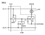
- FIG. 10 is a circuit diagram illustrating an example of a pixel of a display device.
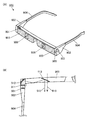
- FIGS. 11A and 11B illustrate an example of an electronic device.
- FIGS. 12A and 12B illustrate an example of an electronic device.
- FIGS. 13A and 13B illustrate an example of an electronic device.
- FIGS. 14A to 14D illustrate an example of an electronic device.
- FIGS. 15A to 15F illustrate an example of an electronic device.
- the word “film” and the word “layer” can be interchanged with each other depending on the case or the situation.
- the term “conductive layer” can be changed to the term “conductive film”.
- the term “insulating film” can be changed to the term “insulating layer”.
- the display device in this embodiment includes a plurality of light-emitting diodes which are display elements and a plurality of transistors which drive the display elements.
- the plurality of light emitting diodes are provided in a matrix on a substrate having a property of transmitting visible light.
- Each of the plurality of transistors is electrically connected to at least one of the plurality of light emitting diodes.
- the plurality of light emitting diodes are located closer to the substrate than the plurality of transistors.
- the plurality of light emitting diodes emit light toward the substrate.
- the display device of this embodiment is formed by bonding a plurality of transistors and a plurality of light-emitting diodes formed over different substrates.
- the method for manufacturing a display device in this embodiment since a plurality of light-emitting diodes and a plurality of transistors are attached at one time, even when a display device with a large number of pixels or a high-definition display device is manufactured, light emission is prevented. Compared with the method of mounting the diodes one by one on a circuit board, the manufacturing time of the display device can be reduced, and the difficulty of manufacturing can be reduced.
- the display device of this embodiment has a function of displaying an image using a light-emitting diode. Since the light-emitting diode is a self-light-emitting element, when a light-emitting diode is used as a display element, the display device does not require a backlight and does not need to include a polarizing plate. Therefore, the power consumption of the display device can be reduced, and the display device can be reduced in thickness and weight. In addition, a display device using a light-emitting diode as a display element has high contrast and a wide viewing angle, so that high display quality can be obtained. In addition, by using an inorganic material as a light-emitting material, the life of a display device can be extended and reliability can be improved.
- a micro LED is used as a light emitting diode.
- a micro LED having a double hetero junction will be described.
- the light emitting diode is not particularly limited, and for example, a micro LED having a quantum well junction, an LED using a nano column, or the like may be used.
- Area of the region that emits light emitting diode is preferably 1 mm 2 or less, more preferably 10000 2 or less, more preferably 3000 .mu.m 2 or less, more preferably 700 .mu.m 2 or less. Note that in this specification and the like, a light-emitting diode whose light-emitting region has an area of 10000 ⁇ m 2 or less may be referred to as a micro LED.
- the transistor included in the display device preferably includes a metal oxide in a channel formation region.
- a transistor including a metal oxide can have low power consumption. Therefore, by combining with a micro LED, a display device with extremely low power consumption can be realized.
- the display device of this embodiment preferably includes a transistor in which the height of the upper surface of the gate electrode is approximately equal to the height of the upper surface of the insulating layer.
- the upper surface of the gate electrode and the upper surface of the insulating layer are flattened, and the height of the upper surface of the gate electrode is made equal to the height of the upper surface of the insulating layer. be able to.
- the transistor having such a structure can be easily reduced in size. Since the size of the pixel can be reduced by reducing the size of the transistor, the definition of the display device can be increased.
- the display device of this embodiment can increase definition, the display device can be suitably used for an electronic device having a relatively small display portion.
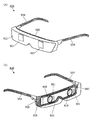
- electronic devices include wristwatch-type or bracelet-type information terminals (wearable devices), devices for VR (Virtual Reality) such as head-mounted displays, glasses-type devices for AR (Augmented Reality), and MR.
- Wearable devices that can be worn on the head, such as devices for (Mixed Reality).
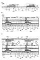
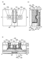
- FIG. 1 shows a cross-sectional view of the display device 100A.
- FIG. 2 is a cross-sectional view illustrating a method for manufacturing the display device 100A.
- the display device 100A shown in FIG. 1 is configured by bonding an LED substrate 150A shown in FIG. 2A and a circuit substrate 150B shown in FIG. 2B (see FIG. 2C).
- FIG. 2A is a cross-sectional view of the LED substrate 150A.
- the LED substrate 150A has a substrate 101, a light emitting diode 110a, a light emitting diode 110b, and a protective layer 102.
- the light emitting diode 110a includes an electrode 112a, a semiconductor layer 113a, a light emitting layer 114a, a semiconductor layer 115a, and an electrode 116a.
- the light emitting diode 110b includes an electrode 112b, a semiconductor layer 113b, a light emitting layer 114b, a semiconductor layer 115b, and an electrode 116b.
- the electrode 112a is electrically connected to the semiconductor layer 113a.
- the electrode 116a is electrically connected to the semiconductor layer 115a.
- the electrode 112b is electrically connected to the semiconductor layer 113b.
- the electrode 116b is electrically connected to the semiconductor layer 115b.
- the protective layer 102 is provided so as to cover the substrate 101, the semiconductor layers 113a and 113b, the light-emitting layers 114a and 114b, and the semiconductor layers 115a and 115b.
- the protective layer 102 covers the side surfaces of the electrodes 112a and 112b and the side surfaces of the electrodes 116a and 116b, and has openings overlapping with the upper surfaces of the electrodes 112a and 112b and the upper surfaces of the electrodes 116a and 116b. In the opening, the upper surfaces of the electrodes 112a and 112b and the upper surfaces of the electrodes 116a and 116b are exposed.
- the light emitting layer 114a is sandwiched between the semiconductor layers 113a and 115a.
- the light emitting layer 114b is sandwiched between the semiconductor layers 113b and 115b. In the light emitting layers 114a and 114b, electrons and holes are combined to emit light.
- One of the semiconductor layers 113a and 113b and the semiconductor layers 115a and 115b is an n-type semiconductor layer, and the other is a p-type semiconductor layer.
- the stacked structure including the semiconductor layer 113a, the light-emitting layer 114a, and the semiconductor layer 115a, and the stacked structure including the semiconductor layer 113b, the light-emitting layer 114b, and the semiconductor layer 115b are light sources of red, yellow, green, and blue, respectively. Is formed. Preferably, the two stacked structures present light of different colors.
- These laminated structures include, for example, gallium / phosphorus compounds, gallium / arsenic compounds, gallium / aluminum / arsenic compounds, aluminum / gallium / indium / phosphorous compounds, gallium nitride, indium / gallium nitride compounds, selenium / zinc compounds, etc. Can be used.
- the light emitting diode 110a and the light emitting diode 110b so as to exhibit light of different colors, a step of forming a color conversion layer becomes unnecessary. Therefore, the manufacturing cost of the display device can be reduced.
- the two stacked structures may exhibit light of the same color.
- light emitted from the light emitting layers 114a and 114b may be extracted to the outside of the display device through one or both of the color conversion layer and the coloring layer.
- the configuration in which each color pixel has a light emitting diode that emits light of the same color will be described later in Configuration Example 2 of the display device.
- the display device of this embodiment may include a light-emitting diode that emits infrared light.
- a light emitting diode that emits infrared light can be used, for example, as a light source of an infrared light sensor.
- a single crystal substrate such as a sapphire (Al 2 O 3 ) substrate, a silicon carbide (SiC) substrate, a silicon (Si) substrate, and a gallium nitride (GaN) substrate can be used.
- the substrate 101 has a property of transmitting visible light. For example, by reducing the thickness by polishing or the like, the transmittance of the substrate 101 with respect to visible light can be increased.
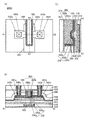
- FIG. 2B is a cross-sectional view of the circuit board 150B.
- the circuit board 150B includes a substrate 151, an insulating layer 152, a transistor 120a, a transistor 120b, a conductive layer 184a, a conductive layer 184b, a conductive layer 187, a conductive layer 189, an insulating layer 186, an insulating layer 188, a conductive layer 190a, a conductive layer 190b, It has a conductive layer 190c and a conductive layer 190d.
- the circuit board 150B further includes insulating layers such as an insulating layer 162, an insulating layer 181, an insulating layer 182, an insulating layer 183, and an insulating layer 185. One or more of these insulating layers may be regarded as a component of the transistor in some cases; however, in this embodiment, description will be made without including the component in the transistor.
- an insulating substrate such as a glass substrate, a quartz substrate, a sapphire substrate, or a ceramic substrate, a single crystal semiconductor substrate made of a material such as silicon or silicon carbide, a polycrystalline semiconductor substrate, or a compound semiconductor substrate such as silicon germanium And a semiconductor substrate such as an SOI substrate.
- the substrate 151 preferably blocks visible light (has non-transparency with respect to visible light). When the substrate 151 blocks visible light, light can be prevented from entering the transistors 120a and 120b formed on the substrate 151 from the outside. Note that one embodiment of the present invention is not limited thereto, and the substrate 151 may have a property of transmitting visible light.
- An insulating layer 152 is provided over the substrate 151.
- the insulating layer 152 functions as a barrier layer that prevents impurities such as water and hydrogen from diffusing into the transistors 120a and 120b from the substrate 151 and preventing oxygen from being released from the metal oxide layer 165 to the insulating layer 152 side.
- a film such as an aluminum oxide film, a hafnium oxide film, or a silicon nitride film, to which hydrogen and oxygen are less likely to diffuse than a silicon oxide film can be used.
- Each of the transistors 120a and 120b includes a conductive layer 161, an insulating layer 163, an insulating layer 164, a metal oxide layer 165, a pair of conductive layers 166, an insulating layer 167, a conductive layer 168, and the like.
- the metal oxide layer 165 has a channel formation region.
- the metal oxide layer 165 includes a first region overlapping with one of the pair of conductive layers 166, a second region overlapping with the other of the pair of conductive layers 166, and a region between the first region and the second region. And a third region.
- a conductive layer 161 and an insulating layer 162 are provided over the insulating layer 152, and an insulating layer 163 and an insulating layer 164 are provided so as to cover the conductive layer 161 and the insulating layer 162.
- the metal oxide layer 165 is provided over the insulating layer 164.
- the conductive layer 161 functions as a gate electrode, and the insulating layers 163 and 164 function as gate insulating layers.
- the conductive layer 161 overlaps with the metal oxide layer 165 with the insulating layer 163 and the insulating layer 164 interposed therebetween.
- the insulating layer 163 preferably functions as a barrier layer, similarly to the insulating layer 152.
- an oxide insulating film such as a silicon oxide film is preferably used as the insulating layer 164.
- the height of the upper surface of the conductive layer 161 is approximately equal to the height of the upper surface of the insulating layer 162.
- an opening is provided in the insulating layer 162, the conductive layer 161 is formed so as to fill the opening, and then planarization is performed by a CMP method or the like, so that the height of the upper surface of the conductive layer 161 and the height of the insulating layer 162 are reduced.
- the height of the upper surface can be made uniform.
- the sizes of the transistors 120a and 120b can be reduced.
- the pair of conductive layers 166 is provided separately over the metal oxide layer 165.
- the pair of conductive layers 166 functions as a source and a drain.
- An insulating layer 181 is provided so as to cover the metal oxide layer 165 and the pair of conductive layers 166.
- An insulating layer 182 is provided over the insulating layer 181.
- An opening reaching the metal oxide layer 165 is provided in the insulating layers 181 and 182, and the insulating layer 167 and the conductive layer 168 are embedded in the openings. The opening overlaps the third region.
- the insulating layer 167 overlaps with a side surface of the insulating layer 181 and a side surface of the insulating layer 182.
- the conductive layer 168 overlaps with a side surface of the insulating layer 181 and a side surface of the insulating layer 182 with the insulating layer 167 provided therebetween.
- the conductive layer 168 functions as a gate electrode, and the insulating layer 167 functions as a gate insulating layer.
- the conductive layer 168 overlaps with the metal oxide layer 165 with the insulating layer 167 provided therebetween.
- the height of the upper surface of the conductive layer 168 is approximately equal to the height of the upper surface of the insulating layer 182.
- an opening is provided in the insulating layer 182, the insulating layer 167 and the conductive layer 168 are formed so as to fill the opening, and then planarization treatment is performed, so that the height of the upper surface of the conductive layer 168 and the height of the upper surface of the insulating layer 182 are reduced. Height can be aligned. Thus, the sizes of the transistors 120a and 120b can be reduced.
- an insulating layer 183 and an insulating layer 185 are provided so as to cover upper surfaces of the insulating layer 182, the insulating layer 167, and the conductive layer 168.
- the insulating layers 181 and 183 preferably function as barrier layers, similarly to the insulating layer 152.
- a plug electrically connected to one of the pair of conductive layers 166 and the conductive layer 187 is embedded in an opening provided in the insulating layer 181, the insulating layer 182, the insulating layer 183, and the insulating layer 185.
- the plug preferably includes a conductive layer 184b in contact with a side surface of the opening and one upper surface of the pair of conductive layers 166, and a conductive layer 184a embedded inside the conductive layer 184b. At this time, it is preferable that a conductive material through which hydrogen and oxygen are hardly diffused be used for the conductive layer 184b.
- the conductive layer 187 is provided over the insulating layer 185, and the insulating layer 186 is provided over the conductive layer 187.
- An opening reaching the conductive layer 187 is provided in the insulating layer 186, and the conductive layer 189 is embedded in the opening.
- a conductive layer 187 and an insulating layer 186 may be provided over the insulating layer 185, and an insulating layer 188 may be provided over the conductive layer 187.
- the height of the upper surface of the conductive layer 187 matches or approximately matches the height of the upper surface of the insulating layer 186.
- an opening is provided in the insulating layer 186, the conductive layer 187 is formed so as to fill the opening, and planarization is performed using a CMP method or the like, so that the height of the upper surface of the conductive layer 187 and the height of the insulating layer 186 are reduced.
- the height of the upper surface can be made uniform.
- an opening reaching the conductive layer 187 is provided in the insulating layer 188, and the conductive layer 189 is embedded in the opening.
- the conductive layer 189 functions as a plug for electrically connecting the conductive layer 187 to the conductive layer 190a or 190c.
- One of a pair of conductive layers 166 of the transistor 120a is electrically connected to the conductive layer 190a through the conductive layers 184a, 184b, 187, and 189.
- one of the pair of conductive layers 166 of the transistor 120b is electrically connected to the conductive layer 190c through the conductive layers 184a, 184b, 187, and 189.
- materials that can be used for various conductive layers included in the display device of this embodiment include metals such as aluminum, titanium, chromium, nickel, copper, yttrium, zirconium, molybdenum, silver, tantalum, and tungsten; Alternatively, an alloy containing this as a main component may be used. Further, a film containing any of these materials can be used as a single layer or a stacked structure. For example, a single-layer structure of an aluminum film containing silicon, a two-layer structure of stacking an aluminum film on a titanium film, a two-layer structure of stacking an aluminum film on a tungsten film, and a copper film on a copper-magnesium-aluminum alloy film.
- a two-layer structure in which a copper film is stacked on a titanium film a two-layer structure in which a copper film is stacked on a tungsten film, a titanium film or a titanium nitride film, and an aluminum film or a copper film stacked thereon
- an oxide such as indium oxide, tin oxide, or zinc oxide may be used.
- it is preferable to use copper containing manganese since the controllability of the shape by etching is improved.
- materials that can be used for various insulating layers included in the display device of this embodiment include resins such as acrylic, polyimide, epoxy, and silicone; silicon oxide; silicon oxynitride; silicon nitride oxide; silicon nitride; An inorganic insulating material such as aluminum is used.
- circuit board 150B may include one or both of a reflective layer that reflects light of the light-emitting diode and a light-blocking layer that blocks the light.
- the electrodes 112a, 112b, 116a, and 116b provided on the LED board 150A are electrically connected to the conductive layers 190a, 190b, 190c, and 190d provided on the circuit board 150B, respectively.
- the electrode 116a and the conductive layer 190a are electrically connected via the conductor 117a.
- the transistor 120a and the light emitting diode 110a can be electrically connected.
- the electrode 116a functions as a pixel electrode of the light emitting diode 110a.
- the electrode 112a and the conductive layer 190b are electrically connected via the conductor 117b.
- the electrode 112a functions as a common electrode of the light emitting diode 110a.
- the electrode 116b and the conductive layer 190c are electrically connected via the conductor 117c.
- the transistor 120b and the light emitting diode 110b can be electrically connected.
- the electrode 116b functions as a pixel electrode of the light emitting diode 110b.
- the electrode 112b and the conductive layer 190d are electrically connected via a conductor 117d.
- the electrode 112b functions as a common electrode of the light emitting diode 110b.
- a conductive paste such as silver, carbon, or copper, or a bump such as gold or solder can be suitably used.
- the electrodes 112a, 112b, 116a, 116b connected to the conductors 117a to 117d, and the conductive layers 190a to 190d be made of a conductive material having low contact resistance with the conductors 117a to 117d, respectively.
- the conductive material connected thereto is aluminum, titanium, copper, an alloy of silver (Ag), palladium (Pd), and copper (Cu) (Ag-Pd- Cu (APC)) is preferable because the contact resistance is low.
- FIG. 2C shows an example in which the conductors 117a to 117d are provided on the circuit board 150B side and the LED board 150A and the circuit board 150B are attached to each other.
- the conductors 117a to 117d may be provided on the LED substrate 150A side, and the LED substrate 150A and the circuit substrate 150B may be bonded.
- a plurality of light-emitting diodes may be electrically connected to one transistor.
- FIG. 3 shows a cross-sectional view of the display device 100B.
- the transistor 120a and the transistor 120b have different channel lengths.
- Other configurations are the same as those of the display device 100A.
- the transistor 120a for driving the light emitting diode 110a and the transistor 120b for driving the light emitting diode 110b may be different from each other in at least one of transistor size, channel length, channel width, structure, and the like.
- the configuration of the transistor may be changed for each color.
- one or both of the channel length and the channel width of the transistor may be changed for each color in accordance with the amount of current required to emit light with desired luminance.
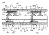
- FIG. 4 shows a cross-sectional view of the display device 100C.
- the display device 100C includes transistors in which a channel formation region is formed over a substrate 131 (transistors 130a and 130b) and transistors each including a channel formation region in a metal oxide (transistors 120a and 120b) are stacked.
- Each of the transistors 130a and 130b includes a conductive layer 135, an insulating layer 134, an insulating layer 136, and a pair of low-resistance regions 133.
- the conductive layer 135 functions as a gate.
- the insulating layer 134 is located between the conductive layer 135 and the substrate 131 and functions as a gate insulating layer.
- the insulating layer 136 is provided to cover a side surface of the conductive layer 135 and functions as a sidewall.
- the pair of low-resistance regions 133 is a region in the substrate 131 to which impurities are doped, and one functions as a source of the transistor and the other functions as a drain of the transistor.
- an element isolation layer 132 is provided between two adjacent transistors so as to be embedded in the substrate 131.
- An insulating layer 139 is provided to cover the transistors 130a and 130b, and a conductive layer 138 is provided over the insulating layer 139.
- the conductive layer 138 is electrically connected to one of the pair of low-resistance regions 133 through the conductive layer 137 embedded in the opening of the insulating layer 139.
- An insulating layer 141 is provided to cover the conductive layer 138, and the conductive layer 142 is provided over the insulating layer 141.
- the conductive layers 138 and 142 each function as a wiring.
- An insulating layer 143 and an insulating layer 152 are provided so as to cover the conductive layer 142.
- the transistors 120a and 120b are provided over the insulating layer 152. Since the laminated structure from the insulating layer 152 to the substrate 101 is the same as that of the display device 100A, a detailed description is omitted.
- the transistors 120a and 120b can be used as transistors included in a pixel circuit.
- the transistors 130a and 130b can be used as a transistor included in a pixel circuit or a transistor included in a driver circuit (one or both of a gate driver and a source driver) for driving the pixel circuit. Further, the transistors 120a, 120b, 130a, and 130b can be used as transistors included in various circuits such as an arithmetic circuit and a memory circuit.
- a pixel circuit not only a pixel circuit but also a driver circuit and the like can be formed directly below the light-emitting diode, so that the size of the display device is reduced as compared to a case where a driver circuit is provided outside the display portion. be able to. Further, a display device with a narrow frame (a narrow non-display area) can be realized.
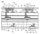
- FIG. 5A is a cross-sectional view of the display device 100D
- FIG. 5B is a cross-sectional view of the display device 100E.
- each color pixel has a light emitting diode that emits light of the same color.
- the display device 100D and the display device 100E include the substrate 191 provided with the coloring layer CFR and the color conversion layer CCMR.
- the substrate 191 has a coloring layer CFR and a color conversion layer CCMR in a region overlapping with the light emitting diode 110a included in the red pixel.
- the color conversion layer CCMR has a function of converting blue light into red light.
- the substrate 191 similarly includes a green coloring layer and a color conversion layer that converts blue light to green in a region overlapping with a light emitting diode included in a green pixel.
- the light emitted from the light emitting diode of the green pixel is converted from blue to green by the color conversion layer, the purity of the green light is increased by the coloring layer, and the green light is emitted to the outside of the display device.
- the substrate 191 does not have a color conversion layer in a region overlapping with the light emitting diode 110b included in the blue pixel.
- the substrate 191 may include a blue coloring layer in a region overlapping with the light-emitting diode 110b included in the blue pixel.
- a blue coloring layer is provided, the purity of blue light can be increased.
- a blue colored layer is not provided, the manufacturing process can be simplified.
- the blue light emitted from the light emitting diode 110b is emitted to the outside of the display device 100D or the display device 100E through the adhesive layer 192 and the substrate 191.
- the substrate 191 Since the substrate 191 is located on the side from which light from the light-emitting diode is extracted, it is preferable to use a material having high transparency to visible light. Examples of a material that can be used for the substrate 191 include glass, quartz, sapphire, and resin. A film such as a resin film may be used for the substrate 191. This makes it possible to reduce the weight and thickness of the display device.
- quantum dots have narrow emission spectrum peak widths and can emit light with good color purity. Thereby, the display quality of the display device can be improved.
- the color conversion layer can be formed by a droplet discharge method (for example, an inkjet method), a coating method, an imprint method, various printing methods (screen printing, offset printing), or the like. Further, a color conversion film such as a quantum dot film may be used.
- the material constituting the quantum dot is not particularly limited, and may be, for example, a Group 14 element, a Group 15 element, a Group 16 element, a compound composed of a plurality of Group 14 elements, or a Group 4 to Group 14 element.
- a compound of an element and a group 16 element, a compound of a group 2 element and a group 16 element, a compound of a group 13 element and a group 15 element, a compound of a group 13 element and a group 17 element examples include compounds of Group 14 elements and Group 15 elements, compounds of Group 11 elements and Group 17 elements, iron oxides, titanium oxides, chalcogenide spinels, and various semiconductor clusters.
- quantum dots examples include a core type, a core-shell type, and a core-multi-shell type.
- quantum dots have a high ratio of surface atoms, and therefore have high reactivity and are likely to aggregate. Therefore, it is preferable that a protective agent is attached to the surface of the quantum dot or a protective group is provided. When the protective agent is attached or the protective group is provided, aggregation can be prevented and solubility in a solvent can be increased. It is also possible to reduce reactivity and improve electrical stability.
- the size of the quantum dot is appropriately adjusted so that light of a desired wavelength is obtained.
- the emission of the quantum dot shifts to the blue side, that is, to the higher energy side.
- the size (diameter) of the quantum dot is, for example, 0.5 nm or more and 20 nm or less, preferably 1 nm or more and 10 nm or less.
- the shape of the quantum dot is not particularly limited, and may be spherical, rod-shaped, disk-shaped, or other shapes.
- a quantum rod, which is a rod-like quantum dot, has a function of exhibiting directional light.
- the coloring layer is a colored layer that transmits light in a specific wavelength range.
- a color filter that transmits light in a red, green, blue, or yellow wavelength range can be used.
- a material that can be used for the coloring layer a metal material, a resin material, a resin material containing a pigment or a dye, or the like can be given.
- the display device 100D first attaches a circuit board and an LED substrate like the display device 100A, and then peels off the substrate 101 included in the LED substrate. It can be manufactured by bonding a substrate 191 provided with a CFR, a color conversion layer CCMR, and the like.
- a method for peeling the substrate 101 there is no limitation on a method for peeling the substrate 101, and, for example, a method of irradiating the entire surface of the substrate 101 with a laser beam (Laser @ beam) as illustrated in FIG. Accordingly, the substrate 101 is separated, so that the protective layer 102 and the light-emitting diodes 110a and 110b can be exposed (FIG. 6B).
- a laser beam Laser @ beam
- an excimer laser As a laser, an excimer laser, a solid-state laser, or the like can be used.
- a diode-pumped solid-state laser DPSS
- DPSS diode-pumped solid-state laser
- a separation layer may be provided between the substrate 101 and the light emitting diodes 110a and 110b.
- the release layer can be formed using an organic material or an inorganic material.
- Examples of the organic material that can be used for the release layer include a polyimide resin, an acrylic resin, an epoxy resin, a polyamide resin, a polyimide amide resin, a siloxane resin, a benzocyclobutene-based resin, and a phenol resin.
- the release layer As an inorganic material that can be used for the release layer, tungsten, molybdenum, titanium, tantalum, niobium, nickel, cobalt, zirconium, zinc, ruthenium, rhodium, palladium, osmium, iridium, a metal containing an element selected from silicon, An alloy containing the element, a compound containing the element, or the like can be given.
- the crystal structure of the layer containing silicon may be any of amorphous, microcrystalline, and polycrystalline.
- various curable adhesives such as a photocurable adhesive such as an ultraviolet curable adhesive, a reaction curable adhesive, a thermosetting adhesive, and an anaerobic adhesive can be used. Further, an adhesive sheet or the like may be used.
- a substrate 191 provided with a coloring layer CFR, a color conversion layer CCMR, and the like may be attached to the substrate 101 with an adhesive layer 192. That is, the substrate 101 need not be peeled off.
- the thickness of the substrate 101 it is preferable to reduce the thickness of the substrate 101 by polishing or the like.
- the efficiency of extracting light emitted from the light emitting diode can be increased.
- the display device can be made thinner and lighter.
- the display device 100E first attaches a circuit substrate and an LED substrate like the display device 100A, and then polishes the substrate 101 included in the LED substrate, and applies a color to the polished surface of the substrate 101 by using an adhesive layer 192. It can be manufactured by bonding a substrate 191 provided with a layer CFR, a color conversion layer CCMR, and the like.
- FIG. 7 shows a cross-sectional view of the display device 100F.
- the display device of one embodiment of the present invention may be a display device provided with a touch sensor (also referred to as an input / output device or a touch panel).
- a touch sensor also referred to as an input / output device or a touch panel.
- the configuration of each display device described above can be applied to a touch panel.
- the display device 100F is an example in which a touch sensor is mounted on the display device 100A.
- sensing element also referred to as a sensor element
- Various sensors capable of detecting the proximity or contact of a detection target such as a finger or a stylus can be applied as the detection element.
- a sensor system various systems such as a capacitance system, a resistive film system, a surface acoustic wave system, an infrared system, an optical system, and a pressure-sensitive system can be used.
- a touch panel having a capacitive sensing element will be described as an example.
- Examples of the capacitance type include a surface type capacitance type and a projection type capacitance type.
- the projection type capacitance method there are a self capacitance method, a mutual capacitance method, and the like. It is preferable to use the mutual capacitance method because simultaneous multipoint detection becomes possible.
- the touch panel of one embodiment of the present invention has a structure in which a display device and a sensing element which are separately manufactured are bonded to each other, an electrode which forms a sensing element is provided on one or both of a substrate supporting the display element and a counter substrate, or the like.
- Various configurations can be applied.
- the laminated structure from the substrate 151 to the substrate 101 is the same as that of the display device 100A, and thus a detailed description is omitted.
- the conductive layer 187b is electrically connected to the FPC 1 through a conductive layer 189b, a conductive layer 190e, and a conductor 195. Signals and power are supplied to the display device 100F via the FPC 1.
- the conductive layer 187b can be formed using the same material and the same step as the conductive layer 187a.
- the conductive layer 189b can be formed using the same material and the same step as the conductive layer 189a.
- the conductive layer 190e can be formed using the same material and the same process as the conductive layers 190a to 190d.
- an anisotropic conductive film (ACF: Anisotropic Conductive Film) or an anisotropic conductive paste (ACP: Anisotropic Conductive Paste) can be used.
- ACF Anisotropic Conductive Film
- ACP Anisotropic Conductive Paste
- a touch sensor is provided on the substrate 171.
- the substrate 171 and the substrate 101 are attached to each other with an adhesive layer 179 with the surface on which the touch sensor is provided of the substrate 171 facing the substrate 101 side.
- An electrode 177 and an electrode 178 are provided on the substrate 101 side of the substrate 171.
- the electrode 177 and the electrode 178 are formed on the same plane.
- a material that transmits visible light is used for the electrodes 177 and 178.
- the insulating layer 173 is provided so as to cover the electrodes 177 and 178.
- the electrode 174 is electrically connected to two electrodes 178 provided so as to sandwich the electrode 177 through an opening provided in the insulating layer 173.
- a wiring 172 obtained by processing the same conductive layer as the electrodes 177 and 178 is connected to a conductive layer 175 obtained by processing the same conductive layer as the electrode 174.
- the conductive layer 175 is electrically connected to the FPC 2 via the connection body 176.
- the transistors that can be used in the display device of one embodiment of the present invention are not limited to the transistors 120a and 120b illustrated in FIGS.
- a structure example of a transistor which can be used for the display device of one embodiment of the present invention will be described with reference to FIGS.
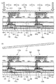
- FIG. 8A is a top view of the transistor 300.
- FIG. 8B is a cross-sectional view taken along dashed-dotted line A1-A2 in FIG.
- FIG. 8B can be a cross-sectional view of the transistor 300 in the channel length direction.
- FIG. 8C is a cross-sectional view taken along dashed-dotted line A3-A4 in FIG.
- FIG. 8C can be a cross-sectional view of the transistor 300 in the channel width direction.
- FIG. 9A is a top view of the transistor 300A. Note that in FIG. 9A, some components are not illustrated for clarity.
- FIG. 9B is a cross-sectional view taken along dashed-dotted line A1-A2 in FIG.
- FIG. 9B can be a cross-sectional view of the transistor 300A in the channel length direction.
- FIG. 9C is a cross-sectional view taken along dashed-dotted line A3-A4 in FIG.
- FIG. 9C can be a cross-sectional view of the transistor 300A in the channel width direction.
- the transistor 300A illustrated in FIG. 9 is a modification example of the transistor 300 illustrated in FIG.
- the oxide layer 330c, the insulating layer 354, and the insulating layer 380 each have a single-layer structure in FIG. 8 and a stacked structure in FIG. Other configurations are the same between FIG. 8 and FIG.
- a transistor is an element having at least three terminals including a gate, a drain, and a source.
- a region where a channel is formed between a drain (a drain terminal, a drain region, or a drain electrode) and a source (a source terminal, a source region, or a source electrode) (hereinafter, also referred to as a channel formation region) is provided.
- current can flow between the source and the drain via the channel formation region.
- a channel formation region refers to a region through which current mainly flows.
- the functions of the source and the drain may be switched when transistors with different polarities are used or when the direction of current changes in circuit operation. For this reason, in this specification and the like, the terms of source and drain may be used interchangeably.
- the channel length refers to, for example, in a top view of a transistor, a region where a semiconductor (or a portion of a semiconductor in which current flows when the transistor is on) and a gate electrode overlap each other, or a source in a channel formation region. It refers to the distance between the (source region or source electrode) and the drain (drain region or drain electrode). Note that in one transistor, the channel length does not always have the same value in all regions. That is, the channel length of one transistor may not be determined to one value. Therefore, in this specification, the channel length is any one of the values, the maximum value, the minimum value, or the average value in the channel formation region.
- the channel width refers to, for example, in a top view of a transistor, a region where a semiconductor (or a portion of a semiconductor in which current flows when the transistor is on) and a gate electrode overlap each other, or a channel formation region in a channel length direction. Refers to the length of the channel formation region in the vertical direction with reference to Note that in one transistor, the channel width does not always have the same value in all regions. That is, the channel width of one transistor may not be determined to one value. Therefore, in this specification, a channel width is any one of values, a maximum value, a minimum value, or an average value in a channel formation region.
- a channel width in a region where a channel is actually formed corresponds to a channel width illustrated in a top view of the transistor.
- apparatus channel width a channel width illustrated in a top view of the transistor.
- the effective channel width becomes larger than the apparent channel width, and the effect may not be ignored.
- the proportion of a channel formation region formed on the side surface of the semiconductor may be large. In that case, the effective channel width is larger than the apparent channel width.
- a simple term "channel width” may refer to an apparent channel width.
- a simple term "channel width” may refer to an effective channel width. The values of the channel length, the channel width, the effective channel width, the apparent channel width, and the like can be determined by analyzing a cross-sectional TEM image or the like.
- the transistor 300 includes a conductive layer 305 which is provided over a substrate (not illustrated) with an insulating layer 314 interposed therebetween and is embedded in the insulating layer 316 and an insulating layer which is provided over the insulating layer 316 and the conductive layer 305.
- the layer 342b part of the top surface of the insulating layer 324, the side surface of the oxide layer 330a, the side surface of the oxide layer 330b, the side surface and the top surface of the conductive layer 342a, and the side surface and the like of the conductive layer 342b. Having an insulating layer 354 disposed in contact with the upper surface.
- An insulating layer 380, an insulating layer 374, and an insulating layer 381 each serving as an interlayer film are provided over the transistor 300.
- the transistor 300 is electrically connected to the conductive layer 340 functioning as a plug (the conductive layers 340a and 340b).
- the insulating layer 341 (the insulating layer 341a and the insulating layer 341b) is provided in contact with a side surface of the conductive layer 340.
- the oxide layer 330 includes an oxide layer 330a provided over the insulating layer 324, an oxide layer 330b provided over the oxide layer 330a, and an oxide layer 330b provided at least partially over the oxide layer 330b.
- An oxide layer 330c which is in contact with the upper surface of the layer 330b. With the oxide layer 330a provided below the oxide layer 330b, diffusion of impurities from a structure formed below the oxide layer 330a to the oxide layer 330b can be suppressed. In addition, when the oxide layer 330c is provided over the oxide layer 330b, diffusion of impurities from a structure formed above the oxide layer 330c to the oxide layer 330b can be suppressed.
- the transistor 300 has an example in which the oxide layer 330 has a three-layer structure of the oxide layer 330a, the oxide layer 330b, and the oxide layer 330c, the present invention is not limited to this.
- the oxide layer 330 is, for example, a single layer of the oxide layer 330b, a two-layer structure of the oxide layer 330a and the oxide layer 330b, a two-layer structure of the oxide layer 330b and the oxide layer 330c, or a stack of four or more layers. It may be a structure. Further, each of the oxide layer 330a, the oxide layer 330b, and the oxide layer 330c may have a stacked structure.
- the conductive layer 342 (the conductive layer 342a and the conductive layer 342b) is provided over the oxide layer 330b.
- the thickness of the conductive layer 342 can be, for example, 1 nm to 50 nm, preferably 2 nm to 25 nm.
- the conductive layer 360 functions as a first gate (also referred to as a top gate) electrode of the transistor 300, and the conductive layers 342a and 342b each function as a source electrode or a drain electrode of the transistor 300.
- a metal oxide functioning as a semiconductor (hereinafter, also referred to as an oxide semiconductor) is preferably used for the oxide layer 330 including a channel formation region.
- an oxide semiconductor for a channel formation region of a transistor, a transistor with high field-effect mobility can be realized. Further, a highly reliable transistor can be realized.
- a metal oxide having a band gap of 2.0 eV or more, preferably 2.5 eV or more is preferable to use.
- a metal oxide having a large band gap for the oxide layer 330 the off-state current of the transistor can be reduced.
- a display device with low power consumption can be provided.
- an In-M-Zn oxide containing indium (In), an element M, and zinc (Zn) (the element M is aluminum, gallium, yttrium, tin, copper, vanadium, beryllium, or boron) , Titanium, iron, nickel, germanium, zirconium, molybdenum, lanthanum, cerium, neodymium, hafnium, tantalum, tungsten, magnesium, or the like).
- the element M aluminum, gallium, yttrium, or tin is preferably used.
- the oxide layer 330 may be formed using an In-M oxide, an In-Zn oxide, or an M-Zn oxide.
- a metal oxide having a low carrier density be used for the transistor 300.
- the impurity concentration in the metal oxide may be reduced and the defect state density may be reduced.
- a low impurity concentration and a low density of defect states are referred to as high-purity intrinsic or substantially high-purity intrinsic.
- impurities in the metal oxide include hydrogen, nitrogen, an alkali metal, an alkaline earth metal, iron, nickel, and silicon.
- hydrogen contained in a metal oxide reacts with oxygen bonded to a metal atom to form water, which may form oxygen vacancies in the metal oxide. If the channel formation region in the metal oxide contains oxygen vacancies, the transistor might have normally-on characteristics. Further, a defect in which hydrogen is contained in an oxygen vacancy functions as a donor, and an electron serving as a carrier may be generated. Further, in some cases, part of hydrogen is bonded to oxygen which is bonded to a metal atom to generate electrons serving as carriers. Therefore, a transistor including a metal oxide containing a large amount of hydrogen is likely to have normally-on characteristics.
- the hydrogen concentration obtained by secondary ion mass spectrometry is less than 1 ⁇ 10 20 atoms / cm 3 , preferably 1 ⁇ 10 19 atoms / cm 3. It is less than 3 , more preferably less than 5 ⁇ 10 18 atoms / cm 3 , further preferably less than 1 ⁇ 10 18 atoms / cm 3 .
- a metal oxide in which impurities such as hydrogen are sufficiently reduced is used for a channel formation region of a transistor, stable electric characteristics can be provided.
- oxygen in the oxide layer 330 diffuses into the conductive layer 342 when the conductive layer 342 (the conductive layers 342a and 342b) and the oxide layer 330 are in contact with each other.
- the conductive layer 342 may be oxidized.
- the conductivity of the conductive layer 342 is likely to decrease. Note that diffusion of oxygen in the oxide layer 330 into the conductive layer 342 can be referred to as that the conductive layer 342 absorbs oxygen in the oxide layer 330.
- Oxygen in the oxide layer 330 diffuses into the conductive layer 342 (the conductive layer 342a and the conductive layer 342b), so that the conductive layer 342a and the oxide layer 330b and the oxide layer 330c and the conductive layer 342b In some cases, a layer may be formed between the oxide layer 330b and the oxide layer 330c. Since the layer contains more oxygen than the conductive layer 342, it is estimated that the layer has insulating properties. At this time, the three-layer structure of the conductive layer 342, the layer, and the oxide layer 330b or the oxide layer 330c can be regarded as a three-layer structure including a metal-insulator-semiconductor and a MIS (Metal-Insulator). -Semiconductor structure.
- the conductive layer 342 (the conductive layer 342a and the conductive layer 342b) has a property in which hydrogen in the oxide layer 330 is easily diffused into the conductive layer 342 and oxygen in the oxide layer 330 is hardly diffused into the conductive layer 342. It is preferable to be formed of a conductive material having Accordingly, hydrogen in the oxide layer 330 diffuses into the conductive layer 342, so that the concentration of hydrogen in the oxide layer 330 is reduced, so that the transistor 300 can have stable electric characteristics. Note that in this specification and the like, the fact that hydrogen in an oxide is easily diffused into a conductive layer is sometimes referred to as that the conductive layer is easy to extract (suck) hydrogen in the oxide in some cases. In addition, the fact that oxygen in an oxide is unlikely to diffuse into a conductive layer may be expressed as, for example, that the conductive layer is hardly oxidized or that the conductive layer has oxidation resistance.
- the conductive material examples include a conductor containing tantalum (Ta), titanium (Ti), or the like.
- a conductor containing tantalum is preferably used for the conductive layer 342.
- the conductor containing tantalum may have nitrogen or oxygen. Therefore, the conductor comprising tantalum, composition formula TaN x O y (x is greater 1.67 following a real number from 0 and, y is a real number of 0 or more and 1.0 or less) is preferably satisfied.
- the conductor containing tantalum includes metal tantalum, tantalum oxide, tantalum nitride, tantalum oxynitride, tantalum oxynitride, and the like. Therefore, in this specification and the like, a conductor containing tantalum may be referred to as TaN x O y .
- the proportion of tantalum is preferably higher.
- the ratio of nitrogen and oxygen is preferably low, and the values of x and y are preferably small.
- the ratio of nitrogen is preferably higher, and the value of x is preferably higher.
- oxidation of the conductive layer 342 can be suppressed.
- the thickness of a layer formed between the conductive layer 342 and the oxide layer 330 can be reduced.
- hydrogen diffused into the conductive layer 342 may stay in the conductive layer 342 in some cases.
- hydrogen in the oxide layer 330 may be absorbed by the conductive layer 342 in some cases.
- hydrogen in the oxide layer 330 may be transmitted through the conductive layer 342 and released to the structure provided around the conductive layer 342 or to the outside of the transistor 300 in some cases.
- the conductive layer 342 is formed by removing hydrogen in the oxide layer 330 from the conductive layer. It is preferable that a layer formed of a conductive material having a property of easily diffusing into the conductive layer 342 and having a function of suppressing oxidation of the conductive layer 342 be provided between the conductive layer 342 and the oxide layer 330. By providing the layer, a structure in which the conductive layer 342 and the oxide layer 330 are not in contact with each other is provided; thus, the conductive layer 342 can suppress absorption of oxygen of the oxide layer 330.
- the insulating layer 314 preferably functions as an insulating barrier film that prevents impurities such as water and hydrogen from diffusing into the transistor 300 from the substrate side. Therefore, the insulating layer 314 has a function of suppressing diffusion of impurities such as hydrogen atoms, hydrogen molecules, water molecules, nitrogen atoms, nitrogen molecules, nitrogen oxide molecules (N 2 O, NO, NO 2, and the like), and copper atoms. It is preferable to use an insulating material having such a material. Alternatively, it is preferable to use an insulating material having a function of suppressing diffusion of oxygen (for example, at least one of an oxygen atom and an oxygen molecule).
- the function of suppressing the diffusion of an impurity or oxygen means a function of suppressing the diffusion of any one or all of the impurity or the oxygen.
- a film having a function of suppressing diffusion of hydrogen or oxygen includes a film with low permeability to hydrogen or oxygen, a film with low permeability to hydrogen or oxygen, a film with a barrier property to hydrogen or oxygen, May be called a barrier film or the like.
- the barrier film may be referred to as a conductive barrier film.
- the insulating layer 3114 it is preferable to use an aluminum oxide film, a silicon nitride film, or the like as the insulating layer 314. Accordingly, diffusion of impurities such as water and hydrogen from the substrate side to the transistor 300 side with respect to the insulating layer 314 can be suppressed. Alternatively, diffusion of oxygen contained in the insulating layer 324 and the like to the substrate side of the insulating layer 314 can be suppressed.
- the insulating layer 314 may have a stacked structure of two or more layers. In that case, the structure is not limited to a laminated structure made of the same material, and may be a laminated structure made of different materials. For example, a stack of an aluminum oxide film and a silicon nitride film may be used.
- the insulating layer 3114 a silicon nitride film formed by a sputtering method is preferably used. Accordingly, the concentration of hydrogen in the insulating layer 314 can be reduced, and diffusion of impurities such as water and hydrogen from the substrate side to the transistor 300 side from the insulating layer 314 can be further suppressed.
- the insulating layer 316 functioning as an interlayer film preferably has a lower dielectric constant than the insulating layer 314.
- a material having a low dielectric constant as an interlayer film, parasitic capacitance generated between wirings can be reduced.
- a silicon oxide film, a silicon oxynitride film, a silicon nitride oxide film, a silicon nitride film, a silicon oxide film to which fluorine is added, a silicon oxide film to which carbon is added, and a silicon oxide film to which carbon and nitrogen are added Alternatively, a silicon oxide film having holes may be used as appropriate.
- the insulating layer 316 has a low hydrogen concentration and a region in which oxygen is present in excess of the stoichiometric composition (hereinafter, also referred to as an excess oxygen region) or oxygen released by heating (hereinafter, also referred to as excess oxygen). It is preferred to have.
- a silicon oxide film formed by a sputtering method is preferably used as the insulating layer 316.
- entry of hydrogen into the oxide layer 330 can be suppressed, or oxygen can be supplied to the oxide layer 330 to reduce oxygen vacancies in the oxide layer 330. Therefore, it is possible to provide a transistor in which fluctuation in electric characteristics is suppressed, stable electric characteristics are improved, and reliability is improved.
- the insulating layer 316 may have a stacked structure.
- an insulating layer similar to the insulating layer 314 may be provided at least in a portion in contact with a side surface of the conductive layer 305.
- oxidation of the conductive layer 305 due to oxygen contained in the insulating layer 316 can be suppressed.
- the conductive layer 305 can suppress a decrease in the amount of oxygen contained in the insulating layer 316.
- the conductive layer 305 may function as a second gate (also referred to as a bottom gate) electrode in some cases.
- the threshold voltage (V th ) of the transistor 300 can be controlled by changing the potential applied to the conductive layer 305 independently of the potential applied to the conductive layer 360 without changing the potential.
- Vth of the transistor 300 can be further increased and off-state current can be reduced. Therefore, when a negative potential is applied to the conductive layer 305, the drain current when the potential applied to the conductive layer 360 is 0 V can be smaller than when no negative potential is applied.
- the conductive layer 305 is provided so as to overlap with the oxide layer 330 and the conductive layer 360. Further, the conductive layer 305 is preferably provided so as to be embedded in the insulating layer 314 or the insulating layer 316.
- the conductive layer 305 is preferably provided to be larger than a channel formation region in the oxide layer 330 as illustrated in FIG. In particular, as illustrated in FIG. 8C, it is preferable that the conductive layer 305 also extend in a region outside an end portion of the oxide layer 330 that intersects with the channel width direction. That is, it is preferable that the conductive layer 305 and the conductive layer 360 overlap with each other via the insulating layer outside the side surface of the oxide layer 330 in the channel width direction.
- the channel formation region of the oxide layer 330 is electrically surrounded by the electric field of the conductive layer 360 functioning as the first gate electrode and the electric field of the conductive layer 305 functioning as the second gate electrode. be able to.
- the conductive layer 305 is extended to function as a wiring. Note that this embodiment is not limited to this, and a conductive layer functioning as a wiring may be provided below the conductive layer 305. Further, the conductive layer 305 is not necessarily provided for each transistor. For example, a structure in which the conductive layer 305 is shared by a plurality of transistors may be employed.
- the conductive layer 305 has a stacked-layer structure of two layers (a first conductive layer over the insulating layer 314 and a second conductive layer over the first conductive layer) is described.
- the conductive layer 305 may have a single-layer structure or a stacked structure of three or more layers.
- ordinal numbers may be given in the order of formation to distinguish them.
- the first conductive layer of the conductive layer 305 is formed of an impurity such as a hydrogen atom, a hydrogen molecule, a water molecule, a nitrogen atom, a nitrogen molecule, a nitrogen oxide molecule (such as N 2 O, NO, or NO 2 ), or a copper atom. It is preferable to use a conductive material having a function of suppressing diffusion. Alternatively, it is preferable to use a conductive material having a function of suppressing diffusion of oxygen (for example, at least one of an oxygen atom and an oxygen molecule).
- the second conductive layer of the conductive layer 305 is prevented from being oxidized to lower the conductivity. be able to.
- the conductive material having a function of suppressing diffusion of oxygen for example, tantalum, tantalum nitride, ruthenium, ruthenium oxide, or the like is preferably used. Therefore, the first conductive layer of the conductive layer 305 preferably has a single-layer structure or a stacked-layer structure using any of the above conductive materials.
- the first conductive layer of the conductive layer 305 may be a stack of a tantalum film, a tantalum nitride film, a ruthenium film, or a ruthenium oxide film and a titanium film or a titanium nitride film.
- the second conductive layer of the conductive layer 305 a conductive material containing tungsten, copper, or aluminum as a main component is preferably used. Note that in FIG. 8B and the like, the second conductive layer of the conductive layer 305 is illustrated as a single layer; however, a stacked structure may be employed; for example, a titanium film or a titanium nitride film and a film including the conductive material. May be laminated.
- the insulating layers 322 and 324 function as gate insulating layers.
- the insulating layer 322 have a function of suppressing diffusion of hydrogen (for example, at least one of a hydrogen atom and a hydrogen molecule). It is preferable that the insulating layer 322 have a function of suppressing diffusion of oxygen (for example, at least one of oxygen atoms and oxygen molecules). For example, the insulating layer 322 preferably can suppress diffusion of one or both of hydrogen and oxygen more than the insulating layer 324.
- an insulator containing an oxide of one or both of aluminum and hafnium which is an insulating material, may be used. It is preferable to use aluminum oxide, hafnium oxide, an oxide containing aluminum and hafnium (hafnium aluminate), or the like as the insulator.
- the insulating layer 322 emits oxygen from the oxide layer 330 to the substrate side or releases impurities such as hydrogen from the periphery of the transistor 300 to the oxide layer 330. It functions as a layer that suppresses the diffusion of.
- the insulating layer 322 diffusion of impurities such as hydrogen to the inside of the transistor 300 can be suppressed, and generation of oxygen vacancies in the oxide layer 330 can be suppressed. Further, the conductive layer 305 can be prevented from reacting with oxygen included in the insulating layer 324 and the oxide layer 330.
- the insulator may be aluminum oxide, bismuth oxide, germanium oxide, niobium oxide, silicon oxide, titanium oxide, tungsten oxide, yttrium oxide, or zirconium oxide.
- these insulators may be nitrided.
- the insulating layer 322 may be formed by stacking a silicon oxide film, a silicon oxynitride film, or a silicon nitride film over an insulating film containing any of these insulators.
- the insulating layer 322 is formed of, for example, so-called high such as aluminum oxide, hafnium oxide, tantalum oxide, zirconium oxide, lead zirconate titanate (PZT), strontium titanate (SrTiO 3 ), (Ba, Sr) TiO 3 (BST), or the like.
- a single-layer structure or a stacked-layer structure may be formed using an insulating material including a ⁇ k material.
- a problem such as a leak current may occur due to a reduction in the thickness of a gate insulating layer.
- a high-k material is used for an insulating layer functioning as a gate insulating layer, reduction in gate potential at the time of transistor operation can be performed while maintaining the physical thickness.
- the insulating layer 324 in contact with the oxide layer 330 preferably releases oxygen by heating.
- a silicon oxide film, a silicon oxynitride film, or the like may be used as the insulating layer 324 as appropriate.
- oxygen vacancies in the oxide layer 330 can be reduced and the reliability of the transistor 300 can be improved.
- an oxide material from which part of oxygen is released by heating as the insulating layer 324.
- An oxide layer from which oxygen is desorbed by heating has a desorption amount of oxygen molecules of 1.0 ⁇ 10 18 molecules / cm 3 or more, preferably 1.0 ⁇ 10 19 , as determined by TDS (Thermal Desorption Spectroscopy) analysis.
- the oxide layer has a molecular weight of not less than moleculars / cm 3 , more preferably 2.0 ⁇ 10 19 molecules / cm 3 or more, or 3.0 ⁇ 10 20 molecules / cm 3 or more.
- the surface temperature of the film at the time of the TDS analysis is preferably in the range of 100 ° C to 700 ° C, or 100 ° C to 400 ° C.
- the insulating layer 324 preferably has a low hydrogen concentration and an excess oxygen region or excess oxygen.
- the insulating layer 324 may be provided using a material similar to that of the insulating layer 316.
- the insulating layer 322 and the insulating layer 324 may have a stacked structure of two or more layers.
- the structure is not limited to a laminated structure made of the same material, and may be a laminated structure made of different materials.
- the oxide layer 330 preferably has a stacked structure of oxides having different chemical compositions.
- the atomic ratio of the element M to the metal element serving as the main component is equal to the element ratio relative to the metal element serving as the main component in the metal oxide used for the oxide layer 330b. It is preferably larger than the atomic ratio of M.
- the atomic ratio of the element M to In is preferably larger than that in the metal oxide used for the oxide layer 330b.
- the atomic ratio of In to the element M is preferably larger than that in the metal oxide used for the oxide layer 330a.
- a metal oxide which can be used for the oxide layer 330a or the oxide layer 330b can be used.
- the oxide layer 330b and the oxide layer 330c preferably have crystallinity.
- a CAAC-OS c-axis / aligned / crystalline / oxide / semiconductor
- An oxide having crystallinity such as a CAAC-OS, has a high density of impurities and defects (such as oxygen vacancies), high crystallinity, and a dense structure.
- CAAC-OS As the oxide layer 330c, and it is preferable that the c-axis of a crystal included in the oxide layer 330c be substantially perpendicular to a formation surface or an upper surface of the oxide layer 330c.
- the CAAC-OS has a property of easily moving oxygen in a direction perpendicular to the c-axis. Therefore, oxygen included in the oxide layer 330c can be efficiently supplied to the oxide layer 330b.
- the energy level at the bottom of the conduction band of the oxide layer 330a and the oxide layer 330c be higher than the energy level of the bottom of the conduction band of the oxide layer 330b.
- the electron affinity of the oxide layer 330a and the oxide layer 330c is preferably smaller than the electron affinity of the oxide layer 330b.
- the oxide layer 330c is preferably formed using a metal oxide that can be used for the oxide layer 330a. At this time, the main path of the carrier becomes the oxide layer 330b.
- the energy level at the bottom of the conduction band changes gradually.
- the energy level at the bottom of the conduction band at the junction of the oxide layer 330a, the oxide layer 330b, and the oxide layer 330c can be said to be continuously changed or continuously joined.
- the defect state density of the mixed layer formed at the interface between the oxide layers 330a and 330b and the interface between the oxide layers 330b and 330c may be reduced.
- the oxide layer 330a and the oxide layer 330b and the oxide layer 330b and the oxide layer 330c each have a common element other than oxygen as a main component, so that a mixed layer having a low density of defect states is formed. can do.
- the oxide layer 330b is an In-Ga-Zn oxide
- the oxide layer 330a and the oxide layer 330c may be formed using an In-Ga-Zn oxide, a Ga-Zn oxide, gallium oxide, or the like. .
- the above atomic ratio is not limited to the atomic ratio of the formed metal oxide, and the atomic ratio of a sputtering target used for forming the metal oxide is used. It may be.
- the density of defect states at the interface between the oxide layers 330a and 330b and the interface between the oxide layers 330b and 330c can be reduced. Can be lower. Therefore, influence of carrier scattering due to interface scattering is reduced, so that the transistor 300 can have high on-state current and high frequency characteristics.
- the oxide layer 330c may have a stacked structure of two or more layers.
- the oxide layer 330c may include a first oxide layer and a second oxide over the first oxide layer.
- the first oxide layer of the oxide layer 330c preferably contains at least one of the metal elements included in the metal oxide used for the oxide layer 330b, and more preferably contains all of the metal elements.
- an In-Ga-Zn oxide film is used as the first oxide layer of the oxide layer 330c
- an In-Ga-Zn oxide film a Ga-Zn oxide film is used as the second oxide layer of the oxide layer 330c.
- the second oxide layer of the oxide layer 330c preferably suppresses diffusion or transmission of oxygen more than the first oxide layer of the oxide layer 330c.
- oxygen contained in the insulating layer 380 is diffused into the insulating layer 350. Can be suppressed. Therefore, the oxygen is easily supplied to the oxide layer 330b through the first oxide layer of the oxide layer 330c.
- the energy level of the bottom of the conduction band of the second oxide layer of the oxide layers 330a and 330c is lower than the energy level of the bottom of the conduction band of the first oxide layer of the oxide layers 330b and 330c. It is preferably higher than the level.
- the electron affinity of the second oxide layer of the oxide layer 330a and the oxide layer 330c is preferably smaller than the electron affinity of the first oxide layer of the oxide layer 330b and the oxide layer 330c.
- the second oxide layer of the oxide layer 330c is formed using a metal oxide that can be used for the oxide layer 330a, and the first oxide layer of the oxide layer 330c is used for the oxide layer 330b. It is preferable to use a metal oxide that can be used.
- the main path of the carrier may be not only the oxide layer 330b but also the first oxide layer of the oxide layer 330c.
- TaN x O y As the conductive layer 342, TaN x O y described above is preferably used. Note that TaN x O y may include aluminum. Further, for example, titanium nitride, a nitride containing titanium and aluminum, ruthenium oxide, ruthenium nitride, an oxide containing strontium and ruthenium, an oxide containing lanthanum and nickel, or the like may be used. These materials are preferable because they are conductive materials that are difficult to oxidize or materials that maintain conductivity even when oxygen is absorbed.
- the top and side surfaces of the conductive layer 342a, the top and side surfaces of the conductive layer 342b, the side surfaces of the oxide layers 330a and 330b, and the top surface of the insulating layer 324 are provided. It is preferable to touch a part. With such a structure, the insulating layer 380 is separated from the insulating layer 324, the oxide layer 330a, and the oxide layer 330b by the insulating layer 354.
- the insulating layer 354 preferably has a function of suppressing diffusion of one or both of hydrogen and oxygen.
- the insulating layer 354 preferably has a function of suppressing diffusion of one or both of hydrogen and oxygen than the insulating layers 324 and 380. Accordingly, diffusion of hydrogen included in the insulating layer 380 to the oxide layers 330a and 330b can be suppressed. Further, by surrounding the insulating layer 324, the oxide layer 330, and the like with the insulating layer 322 and the insulating layer 354, diffusion of impurities such as water and hydrogen from the outside to the insulating layer 324 and the oxide layer 330 is suppressed. can do. Thus, favorable electrical characteristics and reliability can be given to the transistor 300.
- the insulating layer 354 for example, an insulating film containing an oxide of one or both of aluminum and hafnium may be formed.
- the insulating layer 354 is preferably formed by an atomic layer deposition (ALD: Atomic Layer Deposition) method. Since the ALD method is a film formation method with favorable coverage, formation of a step or the like due to unevenness of the insulating layer 354 can be prevented.
- ALD Atomic Layer Deposition
- an insulating film containing aluminum nitride is preferably used as the insulating layer 354.
- a film having excellent insulating properties and excellent heat conductivity can be obtained, so that heat dissipation of heat generated when the transistor 300 is driven can be improved.
- silicon nitride, silicon nitride oxide, or the like can be used.
- an oxide containing gallium may be used as the insulating layer 354.
- An oxide containing gallium is preferable because it sometimes has a function of suppressing diffusion of one or both of hydrogen and oxygen.
- gallium oxide, gallium zinc oxide, indium gallium zinc oxide, or the like can be used as the oxide containing gallium.
- the ratio of the number of gallium atoms to indium is preferably larger. By increasing the atomic ratio, the insulating property of the oxide film can be increased.
- the insulating layer 350 functions as a gate insulating layer.
- the insulating layer 350 is preferably provided in contact with the upper surface of the oxide layer 330c.
- Examples of the material of the insulating layer 350 include silicon oxide, silicon oxynitride, silicon nitride oxide, silicon nitride, silicon oxide to which fluorine is added, silicon oxide to which carbon is added, silicon oxide to which carbon and nitrogen are added, and oxide having voids. Silicon or the like can be used. In particular, silicon oxide and silicon oxynitride are preferable because they are stable against heat.
- the insulating layer 350 is preferably formed using an insulating film from which oxygen is released by heating, similarly to the insulating layer 324.
- an insulating film from which oxygen is released by heating as an insulating layer 350 in contact with the upper surface of the oxide layer 330c, oxygen is effectively supplied to a channel formation region of the oxide layer 330b. Oxygen deficiency in the channel formation region can be reduced. Therefore, it is possible to provide a transistor in which fluctuation in electric characteristics is suppressed, stable electric characteristics are improved, and reliability is improved.
- the concentration of impurities such as water and hydrogen in the insulating layer 350 is preferably reduced.
- the thickness of the insulating layer 350 is preferably greater than or equal to 1 nm and less than or equal to 20 nm.
- the conductive layer 360 include a conductive layer 360a and a conductive layer 360b over the conductive layer 360a.
- the conductive layer 360a is preferably arranged so as to surround the bottom surface and side surfaces of the conductive layer 360b.
- a conductive material having a function of suppressing diffusion of impurities such as a hydrogen atom, a hydrogen molecule, a water molecule, a nitrogen atom, a nitrogen molecule, a nitrogen oxide molecule, and a copper atom be used for the conductive layer 360a.
- a conductive material having a function of suppressing diffusion of oxygen for example, at least one of an oxygen atom and an oxygen molecule.
- the conductive layer 360b can be prevented from being oxidized by the oxygen contained in the insulating layer 350 and being reduced in conductivity.
- the conductive material having a function of suppressing diffusion of oxygen for example, tantalum, tantalum nitride, ruthenium, ruthenium oxide, or the like is preferably used.
- the conductive layer 360 also functions as a wiring, a conductive material with high conductivity is preferably used.
- the conductive layer 360b can be formed using a conductive material mainly containing tungsten, copper, or aluminum.
- the conductive layer 360b may have a stacked structure, for example, a stacked structure of a titanium film, a titanium nitride film, and a film containing the above conductive material.
- the conductive layer 360 has a two-layer structure of the conductive layer 360a and the conductive layer 360b; however, it may have a single-layer structure or a stacked structure of three or more layers.
- the conductive layer 360 is formed in a self-aligned manner so as to fill an opening formed in the insulating layer 380 or the like. By forming the conductive layer 360 in this manner, the conductive layer 360 can be surely arranged in a region between the conductive layer 342a and the conductive layer 342b without alignment.
- the upper surface of the conductive layer 360 is substantially coincident with the upper surface of the insulating layer 350 and the upper surface of the oxide layer 330c.
- the height of the bottom surface of the conductive layer 360 in a region where the conductive layer 360 and the oxide layer 330b do not overlap with each other with reference to the bottom surface of the insulating layer 322 Is preferably lower than the height of the bottom surface of the oxide layer 330b.
- the conductive layer 360 functioning as a gate electrode covers the side surface and the upper surface of the channel formation region of the oxide layer 330b with the insulating layer 350 or the like interposed therebetween, the electric field of the conductive layer 360 can be reduced by the channel of the oxide layer 330b. It is easy to act on the entire formation region. Thus, the on-state current of the transistor 300 can be increased and frequency characteristics can be improved.
- the insulating layer 380 is provided over the insulating layer 324, the oxide layer 330, and the conductive layer 342 with the insulating layer 354 provided therebetween. Further, the upper surface of the insulating layer 380 may be planarized.
- the insulating layer 380 functioning as an interlayer film preferably has a low dielectric constant. By using a material having a low dielectric constant for the interlayer film, parasitic capacitance generated between wirings can be reduced.
- the insulating layer 380 is preferably provided using, for example, the same material as the insulating layer 316.
- silicon oxide and silicon oxynitride are preferable because they are thermally stable.
- a material such as silicon oxide, silicon oxynitride, or silicon oxide having a hole is preferable because a region containing oxygen which is released by heating can be easily formed.
- the insulating layer 380 preferably has a low hydrogen concentration and an excess oxygen region or excess oxygen.
- the insulating layer 380 may be formed using a material similar to that of the insulating layer 316. Note that the insulating layer 380 may have a stacked structure of two or more layers.
- the insulating layer 374 preferably functions as an insulating barrier film that suppresses diffusion of impurities such as water and hydrogen into the insulating layer 380 from above.
- the insulating layer 374 preferably has a low hydrogen concentration and a function of suppressing diffusion of hydrogen, similarly to the insulating layer 314 and the like.
- the insulating layer 374 preferably contacts the upper surfaces of the conductive layer 360, the insulating layer 350, and the oxide layer 330c. Accordingly, entry of impurities such as hydrogen contained in the insulating layer 381 and the like into the insulating layer 350 can be suppressed. Therefore, adverse effects on electrical characteristics of the transistor and reliability of the transistor can be suppressed.
- an insulating layer 381 functioning as an interlayer film be provided over the insulating layer 374.
- the insulating layer 381 preferably has a low dielectric constant, like the insulating layer 316 and the like.
- the insulating layer 381 preferably has a reduced concentration of impurities such as water and hydrogen in the film, similarly to the insulating layer 324 and the like.
- the conductive layers 340a and 340b are provided in openings formed in the insulating layers 381, 374, 380, and 354.
- the conductive layers 340a and 340b are provided to face each other with the conductive layer 360 interposed therebetween. Note that the height of the upper surfaces of the conductive layers 340a and 340b may be flush with the upper surface of the insulating layer 381.
- an insulating layer 341a is provided in contact with a side wall of the opening of the insulating layer 381, the insulating layer 374, the insulating layer 380, and the insulating layer 354, and a conductive layer 340a is formed in contact with a side surface thereof. At least part of the bottom of the opening is provided with conductive layer 342a, and conductive layer 340a is in contact with conductive layer 342a.
- an insulating layer 341b is provided in contact with sidewalls of openings of the insulating layers 381, 374, 380, and 354, and a conductive layer 340b is formed in contact with side surfaces thereof. At least a portion of the bottom of the opening has conductive layer 342b, and conductive layer 340b is in contact with conductive layer 342b.
- the conductive layers 340a and 340b be formed using a conductive material mainly containing tungsten, copper, or aluminum.
- the conductive layers 340a and 340b may have a stacked structure. Note that although the transistor 300 has a structure in which the conductive layer 340a and the conductive layer 340b are provided as a two-layer stacked structure, the present invention is not limited to this.
- the conductive layer 340 may have a single-layer structure or a stacked structure of three or more layers.
- the insulating layer 341a and the insulating layer 341b for example, an insulating film which can be used for the insulating layer 314, the insulating layer 354, or the like can be used. Since the insulating layer 341a and the insulating layer 341b are provided in contact with the insulating layer 354, impurities such as water and hydrogen contained in the insulating layer 380 and the like diffuse into the oxide layer 330 through the conductive layers 340a and 340b. Can be suppressed. In addition, oxygen contained in the insulating layer 380 can be prevented from being absorbed by the conductive layers 340a and 340b.
- a conductive layer serving as a wiring may be provided in contact with an upper surface of the conductive layer 340a and an upper surface of the conductive layer 340b. It is preferable to use a conductive material whose main component is tungsten, copper, or aluminum for the conductive layer functioning as a wiring. Further, the conductive layer may have a stacked structure, for example, a stacked structure of a titanium film, a titanium nitride film, and a film containing the above conductive material. Note that the conductive layer may be formed so as to be embedded in an opening provided in the insulating layer.
- the resistivity is 1.0 ⁇ 10 13 ⁇ cm or more and 1.0 ⁇ 10 15 ⁇ cm or less, preferably 5.0 ⁇ 10 13 ⁇ cm or more and 5.0 ⁇ 10 14 so as to cover the conductive layer. It is preferable to provide an insulating layer of ⁇ cm or less. By providing an insulating layer having the above-described resistivity over the conductive layer, the insulating layer disperses charges accumulated between wirings of the transistor 300, the conductive layer, and the like while maintaining insulating properties. In addition, it is possible to suppress defective characteristics and electrostatic breakdown of a transistor due to the electric charge and an electronic device including the transistor, which is preferable.
- a plurality of light-emitting diodes and a plurality of transistors can be attached at one time, so that manufacturing cost of the display device can be reduced and yield can be improved.
- a display device with reduced power consumption can be realized by combining a micro LED with a transistor including a metal oxide.
- the size of the transistor can be reduced in the display device of this embodiment, the definition can be easily increased and application to an electronic device having a relatively small display portion can be easily performed.
- the display device of this embodiment includes a plurality of pixels arranged in a matrix of m rows and n columns (m and n are each an integer of 1 or more).
- FIG. 10 shows an example of a circuit diagram of a pixel 200 (i, j) (i is an integer of 1 to m, and j is an integer of 1 to n).
- the pixel 200 (i, j) illustrated in FIG. 10 includes a light-emitting element 210, a switch SW21, a switch SW22, a transistor M, and a capacitor C1.
- the gate of the switch SW21 is electrically connected to the scanning line GL1 (i).
- One of a source and a drain of the switch SW21 is electrically connected to the signal line SL (j), and the other is electrically connected to the gate of the transistor M.
- the gate of the switch SW22 is electrically connected to the scanning line GL2 (i).
- One of a source and a drain of the switch SW22 is electrically connected to the wiring COM, and the other is electrically connected to a gate of the transistor M.
- the gate of the transistor M is electrically connected to one electrode of the capacitor C1, the other of the source and the drain of the switch SW21, and the other of the source and the drain of the switch SW22.
- One of a source and a drain of the transistor M is electrically connected to the wiring CATHODE, and the other is electrically connected to a cathode of the light-emitting element 210.
- the other electrode of the capacitor C1 is electrically connected to the wiring CATHODE.
- the anode of the light-emitting element 210 is electrically connected to the wiring ANODE.
- the scanning line GL1 (i) has a function of supplying a selection signal.
- the scanning line GL2 (i) has a function of supplying a control signal.
- the signal line SL (j) has a function of supplying an image signal.
- a constant potential is supplied to the wiring VCOM, the wiring CATHODE, and the wiring ANODE.
- the anode side of the light emitting element 210 can be set to a high potential, and the cathode side can be set to a lower potential than the anode side.
- the switch SW21 is controlled by a selection signal and functions as a selection transistor for controlling the selection state of the pixel 200.
- the transistor M functions as a driving transistor that controls a current flowing to the light-emitting element 210 according to a potential supplied to a gate.
- the switch SW21 When the switch SW21 is on, the image signal supplied to the signal line SL (j) is supplied to the gate of the transistor M, and the luminance of the light emitting element 210 can be controlled in accordance with the potential.
- the switch SW22 has a function of controlling the gate potential of the transistor M based on a control signal. Specifically, the switch SW22 can supply a potential which makes the transistor M non-conductive to the gate of the transistor M.
- the switch SW22 can be used for controlling a pulse width, for example.
- a current can be supplied from the transistor M to the light-emitting element 210 during a period based on the control signal.
- the light emitting element 210 can express a gray scale based on an image signal and a control signal.
- a transistor including a metal oxide (oxide semiconductor) for a semiconductor layer in which a channel is formed is preferably used.
- a transistor including a metal oxide with a wider band gap and lower carrier density than silicon can achieve extremely low off-state current. Therefore, with the small off-state current, electric charge accumulated in a capacitor connected in series with the transistor can be held for a long time. Therefore, it is particularly preferable to use a transistor to which an oxide semiconductor is applied for the switches SW21 and SW22 connected in series to the capacitor C1. In addition, by using a transistor to which an oxide semiconductor is similarly applied for other transistors, manufacturing cost can be reduced.
- the transistor included in the pixel 200 (i, j) a transistor in which silicon is used for a semiconductor in which a channel is formed can be used. It is particularly preferable to use silicon having high crystallinity, such as single crystal silicon or polycrystalline silicon, because high field-effect mobility can be realized and higher-speed operation can be performed.
- a transistor including an oxide semiconductor may be used for at least one of the transistors, and a transistor including silicon may be used for the other transistors.
- a transistor is illustrated as an n-channel transistor in FIG. 10, a p-channel transistor can be used.
- Transistor Next, a transistor that can be used for a display device is described.
- the structure of the transistor included in the display device is not particularly limited.
- a planar transistor, a staggered transistor, or an inverted staggered transistor may be used.
- a top gate structure or a bottom gate structure may be employed.
- gate electrodes may be provided above and below a channel.
- a transistor included in the display device for example, a transistor including a metal oxide for a channel formation region can be used. Thus, a transistor with extremely low off-state current can be realized.
- a transistor including silicon in a channel formation region may be used as a transistor included in the display device.
- the transistor include a transistor including amorphous silicon, a transistor including crystalline silicon (typically, low-temperature polysilicon), and a transistor including single crystal silicon.
- Metal oxide hereinafter, a metal oxide applicable to a semiconductor layer of a transistor will be described.
- a metal oxide containing nitrogen may be collectively referred to as a metal oxide (metal oxide). Further, a metal oxide containing nitrogen may be referred to as metal oxynitride. For example, a metal oxide containing nitrogen such as zinc oxynitride (ZnON) may be used for the semiconductor layer.
- metal oxide metal oxide
- ZnON zinc oxynitride
- CAAC c-axis @ aligned crystal
- CAC Cloud-Aligned @ Composite
- CAC Cloud-Aligned @ Composite
- OS can be used for the semiconductor layer.
- the CAC-OS or CAC-metal oxide includes a conductive function in part of a material, an insulating function in part of a material, and a semiconductor function as a whole of the material.
- a conductive function is a function of flowing electrons (or holes) serving as carriers
- an insulating function is a function of flowing electrons serving as carriers. It is a function that does not flow.
- the CAC-OS or CAC-metal oxide includes a conductive region and an insulating region.
- the conductive region has the above-described conductive function
- the insulating region has the above-described insulating function.
- a conductive region and an insulating region are separated at a nanoparticle level in a material. Further, the conductive region and the insulating region may be unevenly distributed in the material. In some cases, the conductive region is observed with its periphery blurred and connected in a cloud shape.
- the conductive region and the insulating region each have a size of 0.5 nm to 10 nm, preferably 0.5 nm to 3 nm, and are dispersed in a material. There is.
- CAC-OS or CAC-metal oxide includes components having different band gaps.
- a CAC-OS or a CAC-metal oxide includes a component having a wide gap due to an insulating region and a component having a narrow gap due to a conductive region.
- the carrier when the carrier flows, the carrier mainly flows in the component having the narrow gap.
- the component having the narrow gap acts complementarily to the component having the wide gap, and the carrier flows to the component having the wide gap in conjunction with the component having the narrow gap. Therefore, in the case where the CAC-OS or CAC-metal oxide is used for a channel formation region of a transistor, high current driving capability, that is, a high on-state current and high field-effect mobility can be obtained when the transistor is on.
- CAC-OS or the CAC-metal oxide may be referred to as a matrix composite (metal @ composite) or a metal matrix composite (metal @ matrix @ composite).
- An oxide semiconductor is classified into a single crystal oxide semiconductor and a non-single-crystal oxide semiconductor.
- a non-single-crystal oxide semiconductor for example, a CAAC-OS (c-axis aligned crystalline oxide semiconductor), a polycrystalline oxide semiconductor, an nc-OS (nanocrystalline oxide semiconductor), and a pseudo-amorphous oxide semiconductor (a-like) OS: amorphous-like oxide semiconductor, an amorphous oxide semiconductor, or the like.
- the CAAC-OS has a c-axis orientation and a crystal structure in which a plurality of nanocrystals are connected in an ab plane direction and has a strain.
- the strain refers to a region where the orientation of the lattice arrangement changes between a region where the lattice arrangement is uniform and a region where another lattice arrangement is uniform in a region where a plurality of nanocrystals are connected.
- the nanocrystal is basically a hexagon, but is not limited to a regular hexagon and may be a non-regular hexagon.
- distortion may have a lattice arrangement such as a pentagon and a heptagon.
- a clear crystal grain boundary also referred to as a grain boundary
- the formation of crystal grain boundaries is suppressed by the distortion of the lattice arrangement. This is because the CAAC-OS can tolerate distortion because the arrangement of oxygen atoms is not dense in the ab plane direction, or the bonding distance between atoms changes by substitution with a metal element. That's why.
- the CAAC-OS is a layered crystal in which a layer containing indium and oxygen (hereinafter, an In layer) and a layer containing elements M, zinc, and oxygen (hereinafter, an (M, Zn) layer) are stacked. It tends to have a structure (also called a layered structure).
- indium and the element M can be replaced with each other, and when the element M in the (M, Zn) layer is replaced with indium, it can also be referred to as an (In, M, Zn) layer.
- indium in the In layer is replaced with the element M, it can be referred to as an (In, M) layer.
- CAAC-OS is a metal oxide with high crystallinity.
- CAAC-OS it is difficult to confirm a clear crystal grain boundary; thus, it can be said that electron mobility due to the crystal grain boundary is not easily reduced.
- CAAC-OS impurities and defects oxygen deficiency (V O:. Oxygen vacancy also referred) etc.) with less metal It can also be called an oxide. Therefore, a metal oxide having a CAAC-OS has stable physical properties. Therefore, the metal oxide including the CAAC-OS is resistant to heat and has high reliability.
- the nc-OS has a periodic atomic arrangement in a minute region (for example, a region with a thickness of 1 nm to 10 nm, particularly, a region with a size of 1 nm to 3 nm).
- a minute region for example, a region with a thickness of 1 nm to 10 nm, particularly, a region with a size of 1 nm to 3 nm.
- the nc-OS may not be distinguished from an a-like @ OS or an amorphous oxide semiconductor depending on an analysis method.
- indium-gallium-zinc oxide which is a kind of metal oxide including indium, gallium, and zinc
- IGZO indium-gallium-zinc oxide
- a smaller crystal for example, the above-described nanocrystal
- a large crystal here, a crystal of several mm or a crystal of several cm.
- it may be structurally stable.
- a-like @ OS is a metal oxide having a structure between an nc-OS and an amorphous oxide semiconductor.
- a-like @ OS has voids or low density regions. That is, a-like @ OS has lower crystallinity than the nc-OS and the CAAC-OS.
- Oxide semiconductors have various structures and each have different characteristics.
- the oxide semiconductor of one embodiment of the present invention may include two or more of an amorphous oxide semiconductor, a polycrystalline oxide semiconductor, an a-like @ OS, an nc-OS, and a CAAC-OS.
- the metal oxide film functioning as a semiconductor layer can be formed using one or both of an inert gas and an oxygen gas.
- an inert gas an oxygen gas
- an oxygen gas an oxygen gas
- the flow rate ratio of oxygen (oxygen partial pressure) at the time of forming the metal oxide film is preferably 0% or more and 30% or less, and 5% or more and 30% or less. Is more preferable, and 7% or more and 15% or less are still more preferable.
- the electronic device of this embodiment includes the display device of one embodiment of the present invention in the display portion.
- the display device of one embodiment of the present invention has high display quality and low power consumption.
- the display device of one embodiment of the present invention can easily have high definition and large size. Therefore, it can be used for display portions of various electronic devices.
- Examples of the electronic device include a television device, a desktop or notebook personal computer, a monitor for a computer, a digital signage, an electronic device having a relatively large screen such as a large game machine such as a pachinko machine, and a digital device.
- Examples include a camera, a digital video camera, a digital photo frame, a mobile phone, a portable game machine, a portable information terminal, and a sound reproducing device.
- the display device of one embodiment of the present invention can have higher definition and can be preferably used for an electronic device having a relatively small display portion.
- electronic devices include, for example, wristwatch-type or bracelet-type information terminals (wearable devices), devices for VR such as head-mounted displays, glasses-type devices for AR, devices for MR, etc. It can be suitably used for possible wearable devices and the like.
- the electronic device includes sensors (force, displacement, position, speed, acceleration, angular velocity, rotation speed, distance, light, liquid, magnetism, temperature, chemical substance, sound, time, hardness, electric field, current, voltage Including a function of measuring power, radiation, flow rate, humidity, gradient, vibration, smell or infrared light).
- the electronic device of this embodiment can have various functions. For example, a function of displaying various information (still images, moving images, text images, etc.) on the display unit, a touch panel function, a function of displaying a calendar, date or time, a function of executing various software (programs), a wireless communication It can have a function, a function of reading a program or data recorded on a recording medium, and the like.
- FIG. 11A is a perspective view of a glasses-type electronic device 900.
- the electronic device 900 includes a pair of display panels 901, a pair of housings 902, a pair of optical members 903, a pair of mounting portions 904, and the like.
- the electronic device 900 can project an image displayed on the display panel 901 onto a display area 906 of the optical member 903. Since the optical member 903 has a light-transmitting property, a user can see an image displayed in the display area 906 in a manner superimposed on a transmitted image visually recognized through the optical member 903. Therefore, electronic device 900 is an electronic device capable of performing AR display.
- the display panel 901 included in the electronic device 900 preferably has a function of capturing an image in addition to a function of displaying an image.
- the electronic device 900 can receive light incident on the display panel 901 via the optical member 903, convert the light into an electric signal, and output the electric signal.
- the user's eyes, or the eyes and their surroundings can be imaged and output as image information to an external unit or a calculation unit included in the electronic device 900.
- One housing 902 is provided with a camera 905 that can capture an image of the front.
- one of the housings 902 is provided with a connector to which a wireless receiver or a cable can be connected, so that a video signal or the like can be supplied to the housing 902.
- an acceleration sensor such as a gyro sensor
- the housing 902 is preferably provided with a battery, and can be charged wirelessly or by wire.
- a method for projecting an image on the display area 906 of the electronic device 900 will be described with reference to FIG.
- a display panel 901, a lens 911, and a reflection plate 912 are provided inside the housing 902.
- a portion corresponding to the display area 906 of the optical member 903 has a reflection surface 913 functioning as a half mirror.
- Light 915 emitted from the display panel 901 passes through the lens 911 and is reflected by the reflector 912 toward the optical member 903. Inside the optical member 903, the light 915 repeats total reflection at the end face of the optical member 903, and reaches the reflection surface 913, whereby an image is projected on the reflection surface 913. Accordingly, the user can visually recognize both the light 915 reflected on the reflection surface 913 and the transmitted light 916 transmitted through the optical member 903 (including the reflection surface 913).
- FIG. 11 illustrates an example in which the reflection plate 912 and the reflection surface 913 each have a curved surface.
- the degree of freedom in optical design can be increased and the thickness of the optical member 903 can be reduced as compared with the case where these are flat surfaces.
- the reflecting plate 912 and the reflecting surface 913 may be flat surfaces.
- the reflecting plate 912 a member having a mirror surface can be used, and it is preferable that the reflectivity is high.
- the reflection surface 913 a half mirror using reflection of a metal film may be used. However, if a prism or the like using total reflection is used, the transmittance of the transmitted light 916 can be increased.
- the electronic device 900 preferably has a mechanism for adjusting one or both of the distance and the angle between the lens 911 and the display panel 901. This makes it possible to perform focus adjustment, enlargement and reduction of an image, and the like.
- one or both of the lens 911 and the display panel 901 may be configured to be movable in the optical axis direction.
- Electronic device 900 preferably has a mechanism capable of adjusting the angle of reflection plate 912. By changing the angle of the reflector 912, the position of the display area 906 where an image is displayed can be changed. This makes it possible to arrange the display area 906 at an optimum position according to the position of the user's eyes.
- the display device of one embodiment of the present invention can be applied to the display panel 901. Therefore, the electronic device 900 can perform display with extremely high definition.
- FIGS. 12A and 12B are perspective views of a goggle-type electronic device 950.
- FIG. FIG. 12A is a perspective view illustrating a front, a plane, and a left side of the electronic device 950
- FIG. 12B is a perspective view illustrating a back, a bottom, and a right side of the electronic device 950.
- the electronic device 950 includes a pair of display panels 951, a housing 952, a pair of mounting portions 954, a buffer member 955, a pair of lenses 956, and the like.
- the pair of display panels 951 are provided in positions inside the housing 952 that can be visually recognized through the lens 956.
- the electronic device 950 is an electronic device for VR.
- a user wearing the electronic device 950 can visually recognize an image displayed on the display panel 951 through the lens 956. Further, by displaying different images on the pair of display panels 951, three-dimensional display using parallax can be performed.
- An input terminal 957 and an output terminal 958 are provided on the back side of the housing 952.
- a cable that supplies a video signal from a video output device or the like, power for charging a battery provided in the housing 952, and the like can be connected to the input terminal 957.
- the output terminal 958 can function as, for example, an audio output terminal, and can be connected to an earphone, headphones, or the like. Note that the audio output terminal does not need to be provided when the configuration is such that audio data can be output by wireless communication or when audio is output from an external video output device.
- the electronic device 900 preferably has a mechanism capable of adjusting the left and right positions of the lens 956 and the display panel 951 such that the lens 956 and the display panel 951 are at optimal positions according to the position of the user's eyes. Further, it is preferable to have a mechanism for adjusting the focus by changing the distance between the lens 956 and the display panel 951.
- the display device of one embodiment of the present invention can be applied to the display panel 951. Therefore, the electronic device 950 can perform display with extremely high definition. Thereby, the user can be made to feel high immersion.
- the buffer member 955 is a part that comes into contact with the user's face (forehead, cheek, etc.). When the buffer member 955 is in close contact with the user's face, light leakage can be prevented, and the sense of immersion can be further enhanced. It is preferable to use a soft material for the cushioning member 955 so that the cushioning member 955 adheres to the user's face when the user wears the electronic device 950.
- materials such as rubber, silicone rubber, urethane, and sponge can be used.
- the cushioning member 955 When a material such as a sponge whose surface is covered with cloth or leather (natural leather or synthetic leather) or the like is used as the cushioning member 955, a gap is not easily generated between the user's face and the cushioning member 955, and light leakage is suitable. Can be prevented. It is preferable that a member that touches the user's skin, such as the buffer member 955 and the mounting portion 954, be configured to be removable because cleaning and replacement are easy.
- An electronic device 6500 illustrated in FIG. 13A is a portable information terminal that can be used as a smartphone.
- the electronic device 6500 includes a housing 6501, a display portion 6502, a power button 6503, a button 6504, a speaker 6505, a microphone 6506, a camera 6507, a light source 6508, and the like.
- the display portion 6502 has a touch panel function.
- the display device of one embodiment of the present invention can be applied to the display portion 6502.
- FIG. 13B is a schematic cross-sectional view including the end of the housing 6501 on the microphone 6506 side.
- a protective member 6510 having a light-transmitting property is provided on the display surface side of the housing 6501, and a display panel 6511, an optical member 6512, a touch sensor panel 6513, and a print are provided in a space surrounded by the housing 6501 and the protective member 6510.
- a substrate 6517, a battery 6518, and the like are provided.
- a display panel 6511, an optical member 6512, and a touch sensor panel 6513 are fixed to the protection member 6510 with an adhesive layer (not illustrated).
- a part of the display panel 6511 is folded, and the FPC 6515 is connected to the folded portion.
- An IC 6516 is mounted on the FPC 6515.
- the FPC 6515 is connected to a terminal provided on the printed board 6517.
- the flexible display of one embodiment of the present invention can be applied to the display panel 6511. Therefore, an extremely lightweight electronic device can be realized. Further, since the display panel 6511 is extremely thin, a large-capacity battery 6518 can be mounted while suppressing the thickness of the electronic device. Further, by folding a part of the display panel 6511 and disposing a connection portion with the FPC 6515 behind the pixel portion, an electronic device with a narrow frame can be realized.
- FIG. 14A illustrates an example of a television device.
- a display portion 7000 is incorporated in a housing 7101.
- a structure in which the housing 7101 is supported by the stand 7103 is shown.
- the display device of one embodiment of the present invention can be applied to the display portion 7000.
- the television device 7100 illustrated in FIG. 14A can be operated with an operation switch of the housing 7101 or a separate remote controller 7111.
- the display portion 7000 may be provided with a touch sensor, and the television device 7100 may be operated by touching the display portion 7000 with a finger or the like.
- the remote controller 7111 may include a display unit that displays information output from the remote controller 7111. Channel and volume operations can be performed with an operation key or a touch panel included in the remote controller 7111, and images displayed on the display portion 7000 can be operated.
- the television set 7100 is provided with a receiver, a modem, and the like.
- a general television broadcast can be received by the receiver.
- a modem by connecting to a wired or wireless communication network via a modem, one-way (from sender to receiver) or two-way (such as between sender and receiver, or between receivers) information communication is performed. It is also possible.
- FIG. 14B illustrates an example of a notebook personal computer.
- the laptop personal computer 7200 includes a housing 7211, a keyboard 7212, a pointing device 7213, an external connection port 7214, and the like.
- a display portion 7000 is incorporated in the housing 7211.
- the display device of one embodiment of the present invention can be applied to the display portion 7000.
- FIGS. 14C and 14D show examples of digital signage.
- a digital signage 7300 illustrated in FIG. 14C includes a housing 7301, a display portion 7000, a speaker 7303, and the like. Further, it can have an LED lamp, an operation key (including a power switch or an operation switch), a connection terminal, various sensors, a microphone, and the like.
- FIG. 14D illustrates a digital signage 7400 attached to a column 7401.
- Digital signage 7400 has display portion 7000 provided along the curved surface of column 7401.
- the display device of one embodiment of the present invention can be applied to the display portion 7000.
- the display portion 7000 As the display portion 7000 is wider, the amount of information that can be provided at one time can be increased. In addition, the wider the display portion 7000 is, the more easily it can be noticed by humans, and for example, the advertising effect of the advertisement can be enhanced.
- Applying a touch panel to the display portion 7000 is preferable because not only images or moving images can be displayed on the display portion 7000 but also the user can intuitively operate. In addition, when used for providing information such as route information or traffic information, usability can be improved by intuitive operation.
- the digital signage 7300 or the digital signage 7400 can cooperate with an information terminal 7311 or an information terminal 7411 such as a smartphone possessed by a user by wireless communication.
- an information terminal 7311 or an information terminal 7411 such as a smartphone possessed by a user by wireless communication.
- advertisement information displayed on the display portion 7000 can be displayed on the screen of the information terminal 7311 or the information terminal 7411.
- the display on the display portion 7000 can be switched by operating the information terminal 7311 or the information terminal 7411.
- the digital signage 7300 or the digital signage 7400 can also execute a game using the screen of the information terminal 7311 or the information terminal 7411 as an operation means (controller).
- an unspecified number of users can simultaneously participate in the game and enjoy it.
- a housing 9000 including a display portion 9001, a speaker 9003, operation keys 9005 (including a power switch or an operation switch), a connection terminal 9006, a sensor 9007 (power , Displacement, position, speed, acceleration, angular velocity, rotation speed, distance, light, liquid, magnetism, temperature, chemical substance, sound, time, hardness, electric field, current, voltage, power, radiation, flow, humidity, gradient, vibration , Including a function of measuring odor or infrared light), a microphone 9008, and the like.
- the electronic devices illustrated in FIGS. 15A to 15F have various functions. For example, a function of displaying various information (still images, moving images, text images, and the like) on the display unit, a touch panel function, a function of displaying a calendar, date or time, a function of controlling processing by various software (programs), It can have a wireless communication function, a function of reading and processing a program or data recorded on a recording medium, and the like. Note that the functions of the electronic device are not limited to these, and can have various functions.
- the electronic device may have a plurality of display units.
- a camera or the like provided in an electronic device may have a function of capturing a still image or a moving image and storing it on a recording medium (external or built-in to the camera), a function of displaying the captured image on a display unit, and the like. Good.
- FIGS. 15A to 15F The details of the electronic devices illustrated in FIGS. 15A to 15F are described below.
- FIG. 15A is a perspective view illustrating the portable information terminal 9101.
- the portable information terminal 9101 can be used, for example, as a smartphone.
- the portable information terminal 9101 may include a speaker 9003, a connection terminal 9006, a sensor 9007, and the like.
- the portable information terminal 9101 can display characters and image information on a plurality of surfaces thereof.
- FIG. 15A shows an example in which three icons 9050 are displayed. Further, information 9051 indicated by a dashed rectangle can be displayed on another surface of the display portion 9001.
- Examples of the information 9051 include notification of an incoming call such as an e-mail, an SNS, and a telephone, a title of an e-mail or an SNS, a sender name, a date and time, a time, a remaining battery level, and an antenna reception intensity.
- an icon 9050 or the like may be displayed at a position where the information 9051 is displayed.
- FIG. 15B is a perspective view illustrating the portable information terminal 9102.
- the portable information terminal 9102 has a function of displaying information on three or more surfaces of the display portion 9001.
- information 9052, information 9053, and information 9054 are displayed on different surfaces.
- the user can check the information 9053 displayed at a position observable from above the portable information terminal 9102 with the portable information terminal 9102 stored in the breast pocket of the clothes. The user can check the display without taking out the portable information terminal 9102 from his pocket, and can determine, for example, whether or not to receive a call.
- FIG. 15C is a perspective view illustrating a wristwatch-type portable information terminal 9200.
- the portable information terminal 9200 can be used, for example, as a smart watch. Further, the display portion 9001 is provided with a curved display surface, and can perform display along the curved display surface. Further, the portable information terminal 9200 can perform a hands-free call by, for example, intercommunicating with a headset capable of wireless communication. In addition, the portable information terminal 9200 can also perform data transmission and charging with another information terminal through the connection terminal 9006. Note that the charging operation may be performed by wireless power supply.
- FIGS. 15D to 15F are perspective views showing a foldable portable information terminal 9201.
- FIG. 15D illustrates a state where the portable information terminal 9201 is expanded
- FIG. 15F illustrates a state where the portable information terminal 9201 is folded
- FIG. 15E illustrates a state where one of FIG. 15D and FIG. It is a perspective view of the state in the middle of doing.
- the portable information terminal 9201 has excellent portability in a folded state, and has excellent display browsability due to a seamless large display area in an expanded state.
- a display portion 9001 included in the portable information terminal 9201 is supported by three housings 9000 connected by hinges 9055.
- the display portion 9001 can be bent at a radius of curvature of 0.1 mm or more and 150 mm or less.
Landscapes
- Engineering & Computer Science (AREA)
- Microelectronics & Electronic Packaging (AREA)
- General Physics & Mathematics (AREA)
- Physics & Mathematics (AREA)
- Power Engineering (AREA)
- Computer Hardware Design (AREA)
- Condensed Matter Physics & Semiconductors (AREA)
- Theoretical Computer Science (AREA)
- General Engineering & Computer Science (AREA)
- Manufacturing & Machinery (AREA)
- Human Computer Interaction (AREA)
- Devices For Indicating Variable Information By Combining Individual Elements (AREA)
- Electroluminescent Light Sources (AREA)
- Led Device Packages (AREA)
Priority Applications (8)
| Application Number | Priority Date | Filing Date | Title |
|---|---|---|---|
| JP2020540867A JP7517989B2 (ja) | 2018-09-05 | 2019-08-22 | 表示装置、表示モジュール、及び電子機器 |
| CN201980057735.9A CN112639937B (zh) | 2018-09-05 | 2019-08-22 | 显示装置、显示模块、电子设备及显示装置的制造方法 |
| US17/270,081 US11908850B2 (en) | 2018-09-05 | 2019-08-22 | Display device, display module, electronic device, and method for manufacturing display device |
| CN202310648141.3A CN116759429A (zh) | 2018-09-05 | 2019-08-22 | 显示装置、显示模块、电子设备及显示装置的制造方法 |
| KR1020217007543A KR20210043641A (ko) | 2018-09-05 | 2019-08-22 | 표시 장치, 표시 모듈, 전자 기기, 및 표시 장치의 제작 방법 |
| US18/440,172 US20240304611A1 (en) | 2018-09-05 | 2024-02-13 | Display device, display module, electronic device, and method for manufacturing display device |
| JP2024107866A JP7679531B2 (ja) | 2018-09-05 | 2024-07-04 | 表示装置 |
| JP2025077156A JP2025114706A (ja) | 2018-09-05 | 2025-05-07 | 表示装置 |
Applications Claiming Priority (4)
| Application Number | Priority Date | Filing Date | Title |
|---|---|---|---|
| JP2018-166335 | 2018-09-05 | ||
| JP2018-166336 | 2018-09-05 | ||
| JP2018166336 | 2018-09-05 | ||
| JP2018166335 | 2018-09-05 |
Related Child Applications (2)
| Application Number | Title | Priority Date | Filing Date |
|---|---|---|---|
| US17/270,081 A-371-Of-International US11908850B2 (en) | 2018-09-05 | 2019-08-22 | Display device, display module, electronic device, and method for manufacturing display device |
| US18/440,172 Continuation US20240304611A1 (en) | 2018-09-05 | 2024-02-13 | Display device, display module, electronic device, and method for manufacturing display device |
Publications (1)
| Publication Number | Publication Date |
|---|---|
| WO2020049392A1 true WO2020049392A1 (ja) | 2020-03-12 |
Family
ID=69722321
Family Applications (1)
| Application Number | Title | Priority Date | Filing Date |
|---|---|---|---|
| PCT/IB2019/057065 Ceased WO2020049392A1 (ja) | 2018-09-05 | 2019-08-22 | 表示装置、表示モジュール、電子機器、及び表示装置の作製方法 |
Country Status (6)
| Country | Link |
|---|---|
| US (2) | US11908850B2 (enExample) |
| JP (3) | JP7517989B2 (enExample) |
| KR (1) | KR20210043641A (enExample) |
| CN (2) | CN112639937B (enExample) |
| TW (1) | TWI829746B (enExample) |
| WO (1) | WO2020049392A1 (enExample) |
Cited By (5)
| Publication number | Priority date | Publication date | Assignee | Title |
|---|---|---|---|---|
| JP2022079973A (ja) * | 2020-11-17 | 2022-05-27 | セイコーエプソン株式会社 | 電気光学装置、電気光学装置の製造方法および電子機器 |
| US11400029B2 (en) * | 2019-01-23 | 2022-08-02 | Shofu Inc. | Dental porcelain paste superior in application property |
| JP2022188641A (ja) * | 2021-06-09 | 2022-12-21 | 株式会社ジャパンディスプレイ | 表示装置及び表示装置の製造方法 |
| KR20240007656A (ko) | 2021-05-13 | 2024-01-16 | 가부시키가이샤 한도오따이 에네루기 켄큐쇼 | 전자 기기 |
| EP4170734A4 (en) * | 2020-06-18 | 2024-06-19 | Nichia Corporation | METHOD FOR PRODUCING AN IMAGE DISPLAY DEVICE AND IMAGE DISPLAY DEVICE |
Families Citing this family (15)
| Publication number | Priority date | Publication date | Assignee | Title |
|---|---|---|---|---|
| CN108493209B (zh) * | 2018-05-24 | 2020-06-23 | 京东方科技集团股份有限公司 | 一种显示基板、显示装置以及显示基板的制作方法 |
| CN117316973A (zh) | 2018-09-07 | 2023-12-29 | 株式会社半导体能源研究所 | 显示装置、显示模块及电子设备 |
| WO2020217959A1 (ja) * | 2019-04-23 | 2020-10-29 | 京セラ株式会社 | マイクロled素子基板および表示装置 |
| KR20220017474A (ko) | 2019-06-07 | 2022-02-11 | 가부시키가이샤 한도오따이 에네루기 켄큐쇼 | 복합 디바이스 |
| US11710760B2 (en) * | 2019-06-21 | 2023-07-25 | Semiconductor Energy Laboratory Co., Ltd. | Display device, display module, electronic device, and manufacturing method of display device |
| CN114514618A (zh) * | 2019-09-20 | 2022-05-17 | 德国亚琛工业大学 | 用于针对单个电子运动的分岔的连接部件 |
| JP7609800B2 (ja) | 2019-11-21 | 2025-01-07 | 株式会社半導体エネルギー研究所 | 表示装置の作製方法 |
| KR102882579B1 (ko) * | 2020-04-27 | 2025-11-07 | 삼성디스플레이 주식회사 | 표시 장치 및 그의 제조 방법 |
| FR3112902B1 (fr) * | 2020-07-22 | 2022-12-16 | Aledia | Dispositif optoélectronique flexible et son procédé de fabrication |
| JP7621783B2 (ja) * | 2020-12-10 | 2025-01-27 | スタンレー電気株式会社 | 半導体発光装置及び半導体発光素子の支持基板 |
| JP7761601B2 (ja) | 2021-02-12 | 2025-10-28 | 株式会社半導体エネルギー研究所 | 表示装置、電子機器 |
| CN115148887A (zh) * | 2021-03-31 | 2022-10-04 | 中强光电股份有限公司 | 发光二极管线路基板及其制造方法 |
| US12300174B2 (en) | 2021-08-12 | 2025-05-13 | Semiconductor Energy Laboratory Co., Ltd. | Correction method of display apparatus including pixel and plurality of circuits |
| CN114388486B (zh) * | 2021-12-16 | 2025-07-11 | Tcl华星光电技术有限公司 | 显示面板及其制作方法 |
| CN114068610B (zh) * | 2021-12-16 | 2024-11-22 | 宁波升谱光电股份有限公司 | 一种功率开关器件及其制作方法 |
Citations (8)
| Publication number | Priority date | Publication date | Assignee | Title |
|---|---|---|---|---|
| JP2013137509A (ja) * | 2011-10-18 | 2013-07-11 | Semiconductor Energy Lab Co Ltd | 半導体装置 |
| JP2015501085A (ja) * | 2011-12-22 | 2015-01-08 | オスラム オプト セミコンダクターズ ゲゼルシャフト ミット ベシュレンクテル ハフツングOsram Opto Semiconductors GmbH | 表示装置および表示装置の製造方法 |
| JP2015109252A (ja) * | 2013-04-15 | 2015-06-11 | 株式会社半導体エネルギー研究所 | 発光装置 |
| JP2016174143A (ja) * | 2015-01-26 | 2016-09-29 | 株式会社半導体エネルギー研究所 | 半導体装置およびその製造方法 |
| US20160372514A1 (en) * | 2015-06-16 | 2016-12-22 | Au Optronics Corporation | Light emitting diode display and manufacturing method thereof |
| JP6131374B1 (ja) * | 2016-07-18 | 2017-05-17 | ルーメンス カンパニー リミテッド | マイクロledアレイディスプレイ装置 |
| JP2017538290A (ja) * | 2014-11-18 | 2017-12-21 | オキュラス ブイアール,エルエルシー | 集積型カラーledマイクロディスプレイ |
| WO2018116814A1 (ja) * | 2016-12-22 | 2018-06-28 | シャープ株式会社 | 表示装置および製造方法 |
Family Cites Families (54)
| Publication number | Priority date | Publication date | Assignee | Title |
|---|---|---|---|---|
| JPS6131374Y2 (enExample) | 1980-06-18 | 1986-09-12 | ||
| TW540251B (en) * | 1999-09-24 | 2003-07-01 | Semiconductor Energy Lab | EL display device and method for driving the same |
| JP3973471B2 (ja) | 2001-12-14 | 2007-09-12 | 三洋電機株式会社 | デジタル駆動型表示装置 |
| US7230374B2 (en) * | 2003-09-22 | 2007-06-12 | Samsung Sdi Co., Ltd. | Full color organic light-emitting device having color modulation layer |
| EP1879170A1 (en) | 2006-07-10 | 2008-01-16 | THOMSON Licensing | Current drive for light emitting diodes |
| TWI406589B (zh) | 2008-10-28 | 2013-08-21 | Ind Tech Res Inst | Led光源控制電路與方法,及應用其之影像顯示裝置與照明設備 |
| JP2013145833A (ja) | 2012-01-16 | 2013-07-25 | Fujifilm Corp | Led発光素子用反射基板およびledパッケージ |
| US9159700B2 (en) | 2012-12-10 | 2015-10-13 | LuxVue Technology Corporation | Active matrix emissive micro LED display |
| US9153171B2 (en) | 2012-12-17 | 2015-10-06 | LuxVue Technology Corporation | Smart pixel lighting and display microcontroller |
| US8791474B1 (en) | 2013-03-15 | 2014-07-29 | LuxVue Technology Corporation | Light emitting diode display with redundancy scheme |
| US9252375B2 (en) | 2013-03-15 | 2016-02-02 | LuxVue Technology Corporation | Method of fabricating a light emitting diode display with integrated defect detection test |
| KR101730075B1 (ko) | 2013-03-15 | 2017-04-25 | 애플 인크. | 리던던시 스킴을 갖춘 발광 다이오드 디스플레이 및 통합 결함 검출 테스트를 갖는 발광 다이오드 디스플레이를 제작하는 방법 |
| JP6157178B2 (ja) | 2013-04-01 | 2017-07-05 | ソニーセミコンダクタソリューションズ株式会社 | 表示装置 |
| US8987765B2 (en) | 2013-06-17 | 2015-03-24 | LuxVue Technology Corporation | Reflective bank structure and method for integrating a light emitting device |
| JP6402017B2 (ja) * | 2013-12-26 | 2018-10-10 | 株式会社半導体エネルギー研究所 | 半導体装置 |
| US9231153B2 (en) | 2014-05-30 | 2016-01-05 | Mikro Mesa Technology Co., Ltd. | Micro-light-emitting diode |
| US9105813B1 (en) | 2014-05-30 | 2015-08-11 | Mikro Mesa Technology Co., Ltd. | Micro-light-emitting diode |
| US9590137B2 (en) | 2014-05-30 | 2017-03-07 | Mikro Mesa Technology Co., Ltd. | Light-emitting diode |
| US9219197B1 (en) | 2014-05-30 | 2015-12-22 | Mikro Mesa Technology Co., Ltd. | Micro-light-emitting diode |
| WO2015181678A1 (en) | 2014-05-30 | 2015-12-03 | Semiconductor Energy Laboratory Co., Ltd. | Light-emitting device, display device, and electronic device |
| US10158043B2 (en) | 2014-05-30 | 2018-12-18 | Mikro Mesa Technolgy Co., Ltd. | Light-emitting diode and method for manufacturing the same |
| US9825202B2 (en) | 2014-10-31 | 2017-11-21 | eLux, Inc. | Display with surface mount emissive elements |
| US9917226B1 (en) | 2016-09-15 | 2018-03-13 | Sharp Kabushiki Kaisha | Substrate features for enhanced fluidic assembly of electronic devices |
| CN105700723B (zh) * | 2014-11-28 | 2019-03-08 | 昆山国显光电有限公司 | 一种具有触控装置的有机发光显示器及其制造方法 |
| US9653642B1 (en) * | 2014-12-23 | 2017-05-16 | Soraa Laser Diode, Inc. | Manufacturable RGB display based on thin film gallium and nitrogen containing light emitting diodes |
| CN112436021B (zh) | 2015-02-04 | 2025-06-06 | 株式会社半导体能源研究所 | 半导体装置的制造方法 |
| TWI749726B (zh) | 2015-03-09 | 2021-12-11 | 日商半導體能源研究所股份有限公司 | 發光元件、顯示裝置、電子裝置及照明設備 |
| WO2016203340A1 (ja) | 2015-06-19 | 2016-12-22 | 株式会社半導体エネルギー研究所 | 表示装置の作製方法、表示装置、電子機器、プロジェクター、及びヘッドマウントディスプレイ |
| US20170062749A1 (en) | 2015-09-01 | 2017-03-02 | Semiconductor Energy Laboratory Co., Ltd. | Light-Emitting Element, Light-Emitting Device, Electronic Device, and Lighting Device |
| US20170090246A1 (en) | 2015-09-25 | 2017-03-30 | Semiconductor Energy Laboratory Co., Ltd. | Display device and manufacturing method thereof |
| WO2017098375A1 (en) | 2015-12-11 | 2017-06-15 | Semiconductor Energy Laboratory Co., Ltd. | Display device |
| US10868045B2 (en) | 2015-12-11 | 2020-12-15 | Semiconductor Energy Laboratory Co., Ltd. | Transistor, semiconductor device, and electronic device |
| WO2017115208A1 (en) | 2015-12-28 | 2017-07-06 | Semiconductor Energy Laboratory Co., Ltd. | Device, television system, and electronic device |
| JP2017157724A (ja) | 2016-03-02 | 2017-09-07 | デクセリアルズ株式会社 | 表示装置及びその製造方法、並びに発光装置及びその製造方法 |
| KR102610027B1 (ko) | 2016-03-04 | 2023-12-11 | 삼성디스플레이 주식회사 | 표시 장치 |
| CN107437551B (zh) * | 2016-05-25 | 2020-03-24 | 群创光电股份有限公司 | 显示装置及其制造方法 |
| WO2017217703A1 (en) * | 2016-06-13 | 2017-12-21 | Seoul Semiconductor Co., Ltd | Display apparatus and manufacturing method thereof |
| US10332949B2 (en) | 2016-07-06 | 2019-06-25 | Seoul Semiconductor Co., Ltd. | Display apparatus |
| KR20180020091A (ko) * | 2016-08-17 | 2018-02-27 | 가부시키가이샤 한도오따이 에네루기 켄큐쇼 | 표시 장치 |
| JP6639451B2 (ja) | 2016-09-15 | 2020-02-05 | イーラックス・インコーポレイテッドeLux Inc. | 表面実装型発光素子を有するディスプレイ |
| KR102631259B1 (ko) * | 2016-09-22 | 2024-01-31 | 삼성디스플레이 주식회사 | 디스플레이 장치 |
| KR102651097B1 (ko) | 2016-10-28 | 2024-03-22 | 엘지디스플레이 주식회사 | 발광 다이오드 디스플레이 장치 |
| KR102581601B1 (ko) | 2016-12-13 | 2023-09-21 | 엘지디스플레이 주식회사 | 발광 특성이 향상된 양자 발광다이오드 및 이를 포함하는 양자 발광 장치 |
| WO2018172881A1 (ja) | 2017-03-24 | 2018-09-27 | 株式会社半導体エネルギー研究所 | 半導体装置、表示システム及び電子機器 |
| CN106952941B (zh) * | 2017-05-26 | 2020-10-09 | 上海天马有机发光显示技术有限公司 | 一种显示面板、制作方法及电子设备 |
| KR102374754B1 (ko) * | 2017-09-27 | 2022-03-15 | 엘지디스플레이 주식회사 | 터치 구조물을 포함하는 디스플레이 장치 |
| TWI798308B (zh) | 2017-12-25 | 2023-04-11 | 日商半導體能源研究所股份有限公司 | 顯示器及包括該顯示器的電子裝置 |
| US10784240B2 (en) * | 2018-01-03 | 2020-09-22 | Seoul Viosys Co., Ltd. | Light emitting device with LED stack for display and display apparatus having the same |
| KR102521100B1 (ko) * | 2018-01-08 | 2023-04-14 | 삼성디스플레이 주식회사 | 표시 장치 |
| KR102521582B1 (ko) * | 2018-04-03 | 2023-04-12 | 삼성전자주식회사 | 발광 다이오드 디스플레이 장치 |
| JP7326257B2 (ja) | 2018-05-17 | 2023-08-15 | 株式会社半導体エネルギー研究所 | 表示装置 |
| US11961871B2 (en) | 2018-05-18 | 2024-04-16 | Semiconductor Energy Laboratory Co., Ltd. | Display device, display module, electronic device, and method for fabricating display device |
| US11710760B2 (en) | 2019-06-21 | 2023-07-25 | Semiconductor Energy Laboratory Co., Ltd. | Display device, display module, electronic device, and manufacturing method of display device |
| CN113140661B (zh) * | 2021-04-30 | 2023-01-06 | 上海天马微电子有限公司 | 一种显示面板和显示装置 |
-
2019
- 2019-08-22 US US17/270,081 patent/US11908850B2/en active Active
- 2019-08-22 KR KR1020217007543A patent/KR20210043641A/ko active Pending
- 2019-08-22 WO PCT/IB2019/057065 patent/WO2020049392A1/ja not_active Ceased
- 2019-08-22 CN CN201980057735.9A patent/CN112639937B/zh active Active
- 2019-08-22 CN CN202310648141.3A patent/CN116759429A/zh active Pending
- 2019-08-22 JP JP2020540867A patent/JP7517989B2/ja active Active
- 2019-08-27 TW TW108130547A patent/TWI829746B/zh active
-
2024
- 2024-02-13 US US18/440,172 patent/US20240304611A1/en active Pending
- 2024-07-04 JP JP2024107866A patent/JP7679531B2/ja active Active
-
2025
- 2025-05-07 JP JP2025077156A patent/JP2025114706A/ja active Pending
Patent Citations (8)
| Publication number | Priority date | Publication date | Assignee | Title |
|---|---|---|---|---|
| JP2013137509A (ja) * | 2011-10-18 | 2013-07-11 | Semiconductor Energy Lab Co Ltd | 半導体装置 |
| JP2015501085A (ja) * | 2011-12-22 | 2015-01-08 | オスラム オプト セミコンダクターズ ゲゼルシャフト ミット ベシュレンクテル ハフツングOsram Opto Semiconductors GmbH | 表示装置および表示装置の製造方法 |
| JP2015109252A (ja) * | 2013-04-15 | 2015-06-11 | 株式会社半導体エネルギー研究所 | 発光装置 |
| JP2017538290A (ja) * | 2014-11-18 | 2017-12-21 | オキュラス ブイアール,エルエルシー | 集積型カラーledマイクロディスプレイ |
| JP2016174143A (ja) * | 2015-01-26 | 2016-09-29 | 株式会社半導体エネルギー研究所 | 半導体装置およびその製造方法 |
| US20160372514A1 (en) * | 2015-06-16 | 2016-12-22 | Au Optronics Corporation | Light emitting diode display and manufacturing method thereof |
| JP6131374B1 (ja) * | 2016-07-18 | 2017-05-17 | ルーメンス カンパニー リミテッド | マイクロledアレイディスプレイ装置 |
| WO2018116814A1 (ja) * | 2016-12-22 | 2018-06-28 | シャープ株式会社 | 表示装置および製造方法 |
Cited By (9)
| Publication number | Priority date | Publication date | Assignee | Title |
|---|---|---|---|---|
| US11400029B2 (en) * | 2019-01-23 | 2022-08-02 | Shofu Inc. | Dental porcelain paste superior in application property |
| EP4170734A4 (en) * | 2020-06-18 | 2024-06-19 | Nichia Corporation | METHOD FOR PRODUCING AN IMAGE DISPLAY DEVICE AND IMAGE DISPLAY DEVICE |
| US12464859B2 (en) | 2020-06-18 | 2025-11-04 | Nichia Corporation | Method for manufacturing image display device and image display device |
| JP2022079973A (ja) * | 2020-11-17 | 2022-05-27 | セイコーエプソン株式会社 | 電気光学装置、電気光学装置の製造方法および電子機器 |
| JP7619013B2 (ja) | 2020-11-17 | 2025-01-22 | セイコーエプソン株式会社 | 電気光学装置、電気光学装置の製造方法および電子機器 |
| KR20240007656A (ko) | 2021-05-13 | 2024-01-16 | 가부시키가이샤 한도오따이 에네루기 켄큐쇼 | 전자 기기 |
| JP2022188641A (ja) * | 2021-06-09 | 2022-12-21 | 株式会社ジャパンディスプレイ | 表示装置及び表示装置の製造方法 |
| JP7652632B2 (ja) | 2021-06-09 | 2025-03-27 | 株式会社ジャパンディスプレイ | 表示装置及び表示装置の製造方法 |
| US12431477B2 (en) | 2021-06-09 | 2025-09-30 | Japan Display Inc. | Display device and method for manufacturing the same |
Also Published As
| Publication number | Publication date |
|---|---|
| JP2024127980A (ja) | 2024-09-20 |
| TWI829746B (zh) | 2024-01-21 |
| US11908850B2 (en) | 2024-02-20 |
| JP7517989B2 (ja) | 2024-07-17 |
| JPWO2020049392A1 (ja) | 2021-09-24 |
| TW202025112A (zh) | 2020-07-01 |
| TW202418245A (zh) | 2024-05-01 |
| KR20210043641A (ko) | 2021-04-21 |
| CN112639937B (zh) | 2023-06-23 |
| US20240304611A1 (en) | 2024-09-12 |
| JP2025114706A (ja) | 2025-08-05 |
| CN112639937A (zh) | 2021-04-09 |
| US20210327865A1 (en) | 2021-10-21 |
| JP7679531B2 (ja) | 2025-05-19 |
| CN116759429A (zh) | 2023-09-15 |
Similar Documents
| Publication | Publication Date | Title |
|---|---|---|
| JP7679531B2 (ja) | 表示装置 | |
| US12288799B2 (en) | Display device, display module, electronic device, and manufacturing method of display device | |
| US12334480B2 (en) | Display device, display module, and electronic device | |
| JP7534190B2 (ja) | 表示装置の作製方法 | |
| JP7609800B2 (ja) | 表示装置の作製方法 | |
| KR20220138858A (ko) | 표시 장치 및 전자 기기 |
Legal Events
| Date | Code | Title | Description |
|---|---|---|---|
| 121 | Ep: the epo has been informed by wipo that ep was designated in this application |
Ref document number: 19857115 Country of ref document: EP Kind code of ref document: A1 |
|
| ENP | Entry into the national phase |
Ref document number: 2020540867 Country of ref document: JP Kind code of ref document: A |
|
| NENP | Non-entry into the national phase |
Ref country code: DE |
|
| ENP | Entry into the national phase |
Ref document number: 20217007543 Country of ref document: KR Kind code of ref document: A |
|
| 122 | Ep: pct application non-entry in european phase |
Ref document number: 19857115 Country of ref document: EP Kind code of ref document: A1 |