WO2020045233A1 - 窒化物半導体基板の製造方法、窒化物半導体基板および積層構造体 - Google Patents
窒化物半導体基板の製造方法、窒化物半導体基板および積層構造体 Download PDFInfo
- Publication number
- WO2020045233A1 WO2020045233A1 PCT/JP2019/032850 JP2019032850W WO2020045233A1 WO 2020045233 A1 WO2020045233 A1 WO 2020045233A1 JP 2019032850 W JP2019032850 W JP 2019032850W WO 2020045233 A1 WO2020045233 A1 WO 2020045233A1
- Authority
- WO
- WIPO (PCT)
- Prior art keywords
- layer
- plane
- growth
- dislocation density
- main surface
- Prior art date
- Legal status (The legal status is an assumption and is not a legal conclusion. Google has not performed a legal analysis and makes no representation as to the accuracy of the status listed.)
- Ceased
Links
Images








Classifications
-
- H—ELECTRICITY
- H10—SEMICONDUCTOR DEVICES; ELECTRIC SOLID-STATE DEVICES NOT OTHERWISE PROVIDED FOR
- H10P—GENERIC PROCESSES OR APPARATUS FOR THE MANUFACTURE OR TREATMENT OF DEVICES COVERED BY CLASS H10
- H10P14/00—Formation of materials, e.g. in the shape of layers or pillars
- H10P14/20—Formation of materials, e.g. in the shape of layers or pillars of semiconductor materials
- H10P14/32—Formation of materials, e.g. in the shape of layers or pillars of semiconductor materials characterised by intermediate layers between substrates and deposited layers
- H10P14/3242—Structure
-
- C—CHEMISTRY; METALLURGY
- C30—CRYSTAL GROWTH
- C30B—SINGLE-CRYSTAL GROWTH; UNIDIRECTIONAL SOLIDIFICATION OF EUTECTIC MATERIAL OR UNIDIRECTIONAL DEMIXING OF EUTECTOID MATERIAL; REFINING BY ZONE-MELTING OF MATERIAL; PRODUCTION OF A HOMOGENEOUS POLYCRYSTALLINE MATERIAL WITH DEFINED STRUCTURE; SINGLE CRYSTALS OR HOMOGENEOUS POLYCRYSTALLINE MATERIAL WITH DEFINED STRUCTURE; AFTER-TREATMENT OF SINGLE CRYSTALS OR A HOMOGENEOUS POLYCRYSTALLINE MATERIAL WITH DEFINED STRUCTURE; APPARATUS THEREFOR
- C30B25/00—Single-crystal growth by chemical reaction of reactive gases, e.g. chemical vapour-deposition growth
- C30B25/02—Epitaxial-layer growth
- C30B25/04—Pattern deposit, e.g. by using masks
-
- C—CHEMISTRY; METALLURGY
- C30—CRYSTAL GROWTH
- C30B—SINGLE-CRYSTAL GROWTH; UNIDIRECTIONAL SOLIDIFICATION OF EUTECTIC MATERIAL OR UNIDIRECTIONAL DEMIXING OF EUTECTOID MATERIAL; REFINING BY ZONE-MELTING OF MATERIAL; PRODUCTION OF A HOMOGENEOUS POLYCRYSTALLINE MATERIAL WITH DEFINED STRUCTURE; SINGLE CRYSTALS OR HOMOGENEOUS POLYCRYSTALLINE MATERIAL WITH DEFINED STRUCTURE; AFTER-TREATMENT OF SINGLE CRYSTALS OR A HOMOGENEOUS POLYCRYSTALLINE MATERIAL WITH DEFINED STRUCTURE; APPARATUS THEREFOR
- C30B25/00—Single-crystal growth by chemical reaction of reactive gases, e.g. chemical vapour-deposition growth
- C30B25/02—Epitaxial-layer growth
- C30B25/18—Epitaxial-layer growth characterised by the substrate
- C30B25/183—Epitaxial-layer growth characterised by the substrate being provided with a buffer layer, e.g. a lattice matching layer
-
- C—CHEMISTRY; METALLURGY
- C30—CRYSTAL GROWTH
- C30B—SINGLE-CRYSTAL GROWTH; UNIDIRECTIONAL SOLIDIFICATION OF EUTECTIC MATERIAL OR UNIDIRECTIONAL DEMIXING OF EUTECTOID MATERIAL; REFINING BY ZONE-MELTING OF MATERIAL; PRODUCTION OF A HOMOGENEOUS POLYCRYSTALLINE MATERIAL WITH DEFINED STRUCTURE; SINGLE CRYSTALS OR HOMOGENEOUS POLYCRYSTALLINE MATERIAL WITH DEFINED STRUCTURE; AFTER-TREATMENT OF SINGLE CRYSTALS OR A HOMOGENEOUS POLYCRYSTALLINE MATERIAL WITH DEFINED STRUCTURE; APPARATUS THEREFOR
- C30B25/00—Single-crystal growth by chemical reaction of reactive gases, e.g. chemical vapour-deposition growth
- C30B25/02—Epitaxial-layer growth
- C30B25/18—Epitaxial-layer growth characterised by the substrate
- C30B25/20—Epitaxial-layer growth characterised by the substrate the substrate being of the same materials as the epitaxial layer
-
- C—CHEMISTRY; METALLURGY
- C30—CRYSTAL GROWTH
- C30B—SINGLE-CRYSTAL GROWTH; UNIDIRECTIONAL SOLIDIFICATION OF EUTECTIC MATERIAL OR UNIDIRECTIONAL DEMIXING OF EUTECTOID MATERIAL; REFINING BY ZONE-MELTING OF MATERIAL; PRODUCTION OF A HOMOGENEOUS POLYCRYSTALLINE MATERIAL WITH DEFINED STRUCTURE; SINGLE CRYSTALS OR HOMOGENEOUS POLYCRYSTALLINE MATERIAL WITH DEFINED STRUCTURE; AFTER-TREATMENT OF SINGLE CRYSTALS OR A HOMOGENEOUS POLYCRYSTALLINE MATERIAL WITH DEFINED STRUCTURE; APPARATUS THEREFOR
- C30B29/00—Single crystals or homogeneous polycrystalline material with defined structure characterised by the material or by their shape
- C30B29/10—Inorganic compounds or compositions
- C30B29/40—AIIIBV compounds wherein A is B, Al, Ga, In or Tl and B is N, P, As, Sb or Bi
- C30B29/403—AIII-nitrides
- C30B29/406—Gallium nitride
-
- H—ELECTRICITY
- H10—SEMICONDUCTOR DEVICES; ELECTRIC SOLID-STATE DEVICES NOT OTHERWISE PROVIDED FOR
- H10D—INORGANIC ELECTRIC SEMICONDUCTOR DEVICES
- H10D62/00—Semiconductor bodies, or regions thereof, of devices having potential barriers
- H10D62/40—Crystalline structures
- H10D62/405—Orientations of crystalline planes
-
- H—ELECTRICITY
- H10—SEMICONDUCTOR DEVICES; ELECTRIC SOLID-STATE DEVICES NOT OTHERWISE PROVIDED FOR
- H10D—INORGANIC ELECTRIC SEMICONDUCTOR DEVICES
- H10D62/00—Semiconductor bodies, or regions thereof, of devices having potential barriers
- H10D62/80—Semiconductor bodies, or regions thereof, of devices having potential barriers characterised by the materials
- H10D62/85—Semiconductor bodies, or regions thereof, of devices having potential barriers characterised by the materials being Group III-V materials, e.g. GaAs
- H10D62/8503—Nitride Group III-V materials, e.g. AlN or GaN
-
- H—ELECTRICITY
- H10—SEMICONDUCTOR DEVICES; ELECTRIC SOLID-STATE DEVICES NOT OTHERWISE PROVIDED FOR
- H10P—GENERIC PROCESSES OR APPARATUS FOR THE MANUFACTURE OR TREATMENT OF DEVICES COVERED BY CLASS H10
- H10P14/00—Formation of materials, e.g. in the shape of layers or pillars
- H10P14/20—Formation of materials, e.g. in the shape of layers or pillars of semiconductor materials
- H10P14/24—Formation of materials, e.g. in the shape of layers or pillars of semiconductor materials using chemical vapour deposition [CVD]
-
- H—ELECTRICITY
- H10—SEMICONDUCTOR DEVICES; ELECTRIC SOLID-STATE DEVICES NOT OTHERWISE PROVIDED FOR
- H10P—GENERIC PROCESSES OR APPARATUS FOR THE MANUFACTURE OR TREATMENT OF DEVICES COVERED BY CLASS H10
- H10P14/00—Formation of materials, e.g. in the shape of layers or pillars
- H10P14/20—Formation of materials, e.g. in the shape of layers or pillars of semiconductor materials
- H10P14/27—Formation of materials, e.g. in the shape of layers or pillars of semiconductor materials using selective deposition, e.g. simultaneous growth of monocrystalline and non-monocrystalline semiconductor materials
- H10P14/271—Formation of materials, e.g. in the shape of layers or pillars of semiconductor materials using selective deposition, e.g. simultaneous growth of monocrystalline and non-monocrystalline semiconductor materials characterised by the preparation of substrate for selective deposition
-
- H—ELECTRICITY
- H10—SEMICONDUCTOR DEVICES; ELECTRIC SOLID-STATE DEVICES NOT OTHERWISE PROVIDED FOR
- H10P—GENERIC PROCESSES OR APPARATUS FOR THE MANUFACTURE OR TREATMENT OF DEVICES COVERED BY CLASS H10
- H10P14/00—Formation of materials, e.g. in the shape of layers or pillars
- H10P14/20—Formation of materials, e.g. in the shape of layers or pillars of semiconductor materials
- H10P14/29—Formation of materials, e.g. in the shape of layers or pillars of semiconductor materials characterised by the substrates
- H10P14/2901—Materials
- H10P14/2907—Materials being Group IIIA-VA materials
- H10P14/2908—Nitrides
-
- H—ELECTRICITY
- H10—SEMICONDUCTOR DEVICES; ELECTRIC SOLID-STATE DEVICES NOT OTHERWISE PROVIDED FOR
- H10P—GENERIC PROCESSES OR APPARATUS FOR THE MANUFACTURE OR TREATMENT OF DEVICES COVERED BY CLASS H10
- H10P14/00—Formation of materials, e.g. in the shape of layers or pillars
- H10P14/20—Formation of materials, e.g. in the shape of layers or pillars of semiconductor materials
- H10P14/29—Formation of materials, e.g. in the shape of layers or pillars of semiconductor materials characterised by the substrates
- H10P14/2926—Crystal orientations
-
- H—ELECTRICITY
- H10—SEMICONDUCTOR DEVICES; ELECTRIC SOLID-STATE DEVICES NOT OTHERWISE PROVIDED FOR
- H10P—GENERIC PROCESSES OR APPARATUS FOR THE MANUFACTURE OR TREATMENT OF DEVICES COVERED BY CLASS H10
- H10P14/00—Formation of materials, e.g. in the shape of layers or pillars
- H10P14/20—Formation of materials, e.g. in the shape of layers or pillars of semiconductor materials
- H10P14/32—Formation of materials, e.g. in the shape of layers or pillars of semiconductor materials characterised by intermediate layers between substrates and deposited layers
- H10P14/3202—Materials thereof
- H10P14/3214—Materials thereof being Group IIIA-VA semiconductors
- H10P14/3216—Nitrides
-
- H—ELECTRICITY
- H10—SEMICONDUCTOR DEVICES; ELECTRIC SOLID-STATE DEVICES NOT OTHERWISE PROVIDED FOR
- H10P—GENERIC PROCESSES OR APPARATUS FOR THE MANUFACTURE OR TREATMENT OF DEVICES COVERED BY CLASS H10
- H10P14/00—Formation of materials, e.g. in the shape of layers or pillars
- H10P14/20—Formation of materials, e.g. in the shape of layers or pillars of semiconductor materials
- H10P14/32—Formation of materials, e.g. in the shape of layers or pillars of semiconductor materials characterised by intermediate layers between substrates and deposited layers
- H10P14/3242—Structure
- H10P14/3256—Microstructure
-
- H—ELECTRICITY
- H10—SEMICONDUCTOR DEVICES; ELECTRIC SOLID-STATE DEVICES NOT OTHERWISE PROVIDED FOR
- H10P—GENERIC PROCESSES OR APPARATUS FOR THE MANUFACTURE OR TREATMENT OF DEVICES COVERED BY CLASS H10
- H10P14/00—Formation of materials, e.g. in the shape of layers or pillars
- H10P14/20—Formation of materials, e.g. in the shape of layers or pillars of semiconductor materials
- H10P14/32—Formation of materials, e.g. in the shape of layers or pillars of semiconductor materials characterised by intermediate layers between substrates and deposited layers
- H10P14/3258—Crystal orientation
-
- H—ELECTRICITY
- H10—SEMICONDUCTOR DEVICES; ELECTRIC SOLID-STATE DEVICES NOT OTHERWISE PROVIDED FOR
- H10P—GENERIC PROCESSES OR APPARATUS FOR THE MANUFACTURE OR TREATMENT OF DEVICES COVERED BY CLASS H10
- H10P14/00—Formation of materials, e.g. in the shape of layers or pillars
- H10P14/20—Formation of materials, e.g. in the shape of layers or pillars of semiconductor materials
- H10P14/34—Deposited materials, e.g. layers
- H10P14/3402—Deposited materials, e.g. layers characterised by the chemical composition
- H10P14/3414—Deposited materials, e.g. layers characterised by the chemical composition being group IIIA-VIA materials
- H10P14/3416—Nitrides
-
- H—ELECTRICITY
- H10—SEMICONDUCTOR DEVICES; ELECTRIC SOLID-STATE DEVICES NOT OTHERWISE PROVIDED FOR
- H10P—GENERIC PROCESSES OR APPARATUS FOR THE MANUFACTURE OR TREATMENT OF DEVICES COVERED BY CLASS H10
- H10P14/00—Formation of materials, e.g. in the shape of layers or pillars
- H10P14/20—Formation of materials, e.g. in the shape of layers or pillars of semiconductor materials
- H10P14/34—Deposited materials, e.g. layers
- H10P14/3466—Crystal orientation
-
- H—ELECTRICITY
- H10—SEMICONDUCTOR DEVICES; ELECTRIC SOLID-STATE DEVICES NOT OTHERWISE PROVIDED FOR
- H10P—GENERIC PROCESSES OR APPARATUS FOR THE MANUFACTURE OR TREATMENT OF DEVICES COVERED BY CLASS H10
- H10P95/00—Generic processes or apparatus for manufacture or treatments not covered by the other groups of this subclass
- H10P95/11—Separation of active layers from substrates
-
- H—ELECTRICITY
- H10—SEMICONDUCTOR DEVICES; ELECTRIC SOLID-STATE DEVICES NOT OTHERWISE PROVIDED FOR
- H10D—INORGANIC ELECTRIC SEMICONDUCTOR DEVICES
- H10D8/00—Diodes
- H10D8/60—Schottky-barrier diodes
-
- H—ELECTRICITY
- H10—SEMICONDUCTOR DEVICES; ELECTRIC SOLID-STATE DEVICES NOT OTHERWISE PROVIDED FOR
- H10P—GENERIC PROCESSES OR APPARATUS FOR THE MANUFACTURE OR TREATMENT OF DEVICES COVERED BY CLASS H10
- H10P14/00—Formation of materials, e.g. in the shape of layers or pillars
- H10P14/20—Formation of materials, e.g. in the shape of layers or pillars of semiconductor materials
- H10P14/29—Formation of materials, e.g. in the shape of layers or pillars of semiconductor materials characterised by the substrates
- H10P14/2901—Materials
- H10P14/2921—Materials being crystalline insulating materials
-
- H—ELECTRICITY
- H10—SEMICONDUCTOR DEVICES; ELECTRIC SOLID-STATE DEVICES NOT OTHERWISE PROVIDED FOR
- H10P—GENERIC PROCESSES OR APPARATUS FOR THE MANUFACTURE OR TREATMENT OF DEVICES COVERED BY CLASS H10
- H10P14/00—Formation of materials, e.g. in the shape of layers or pillars
- H10P14/20—Formation of materials, e.g. in the shape of layers or pillars of semiconductor materials
- H10P14/32—Formation of materials, e.g. in the shape of layers or pillars of semiconductor materials characterised by intermediate layers between substrates and deposited layers
- H10P14/3242—Structure
- H10P14/3244—Layer structure
- H10P14/3251—Layer structure consisting of three or more layers
Definitions
- the present invention relates to a method for manufacturing a nitride semiconductor substrate, a nitride semiconductor substrate, and a laminated structure.
- ELO Epi Lateral Overgrowth
- a mask layer having a predetermined opening is formed on a base substrate.
- a facet structure having a triangular cross section is grown on the underlying substrate through the opening of the mask layer.
- a V-shaped groove formed by the facet structure is buried, and a flat crystal layer is obtained.
- the dislocations reaching the surface of the crystal layer are reduced by bending the dislocations during the growth process of the facet structure (for example, Patent Documents 1 and 2).
- the present invention is based on the above-described novel problem found by the inventor, and an object of the present invention is to efficiently reduce the dislocation density on the main surface of a nitride semiconductor substrate.
- a method for manufacturing a nitride semiconductor substrate using a vapor phase growth method Preparing a base substrate made of a single crystal of a group III nitride semiconductor and having a main surface whose closest low-index crystal plane is a (0001) plane; Forming a mask layer having a plurality of openings on the main surface of the base substrate; A single crystal of a group III nitride semiconductor having a top surface with the (0001) plane exposed between a pair of inclined interfaces other than the (0001) plane is formed on the main surface of the base substrate by the opening of the mask layer.
- a method for manufacturing a nitride semiconductor substrate having a distance of more than 100 ⁇ m is provided.
- a nitride semiconductor substrate having a diameter of 2 inches or more and having a main surface whose nearest low-index crystal plane is a (0001) plane,
- the main surface has a low dislocation density region where the dislocation density is less than 1 ⁇ 10 6 cm ⁇ 2 and a high dislocation density where the dislocation density is higher than the dislocation density of the low dislocation density region and 3 ⁇ 10 6 cm ⁇ 2 or less.
- dislocation density regions are alternately arranged,
- a nitride semiconductor substrate is provided in which at least a part of the low dislocation density region has a non-dislocation region of 50 ⁇ m square or more.
- a base substrate made of a single crystal of a group III nitride semiconductor and having a main surface whose nearest low-index crystal plane is a (0001) plane;
- a mask layer provided on the main surface of the base substrate and having a plurality of openings;
- a first low-oxygen-concentration region provided on the main surface of the base substrate and the mask layer through the opening of the mask layer and made of a single crystal of a group III nitride semiconductor;
- a high oxygen concentration region provided on the first low oxygen concentration region and made of a single crystal of a group III nitride semiconductor;
- a second low oxygen concentration region provided on the high oxygen concentration region and made of a single crystal of a group III nitride semiconductor;
- the oxygen concentration of the high oxygen concentration region is higher than the respective oxygen concentrations of the first low oxygen concentration region and the second low oxygen concentration region, When looking at any cross section perpendicular to the main surface,
- An upper surface of the first low oxygen concentration region has at least one valley and a
- the dislocation density on the main surface of the nitride semiconductor substrate can be efficiently reduced.
- FIG. 4 is a flowchart showing a method for manufacturing a nitride semiconductor substrate according to one embodiment of the present invention.
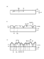
- 1A to 1C are schematic cross-sectional views showing a part of a method for manufacturing a nitride semiconductor substrate according to one embodiment of the present invention.
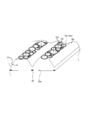
- FIG. 2 is a schematic perspective view showing a part of the method for manufacturing a nitride semiconductor substrate according to one embodiment of the present invention.
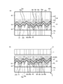
- 1A and 1B are schematic cross-sectional views showing a part of a method for manufacturing a nitride semiconductor substrate according to one embodiment of the present invention.
- 1A and 1B are schematic cross-sectional views showing a part of a method for manufacturing a nitride semiconductor substrate according to one embodiment of the present invention.
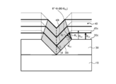
- FIG. 3 is a schematic cross-sectional view showing a growth process under one growth condition.
- FIG. 9 is a schematic cross-sectional view showing a growth process under a second growth condition in which the inclined interface is reduced and the c-plane is enlarged.
- FIG. 3 is a schematic diagram showing an observation image when the main surface of the nitride semiconductor substrate according to one embodiment of the present invention is observed with a multiphoton excitation microscope.
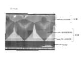
- FIG. 4 is a view showing an observation image obtained by observing a cross section of the laminated structure of Sample 1 with a fluorescence microscope.
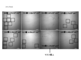
- FIG. 4 is a diagram showing an observation image obtained by observing the surface of the laminated structure of Sample 1 with a multiphoton excitation microscope.
- FIG. 9 is a diagram showing an observation image obtained by observing a cross section of the laminated structure of Sample 2 with a fluorescence microscope.
- FIG. 9 is a diagram showing an observation image obtained by observing a cross section of the laminated structure of Sample 2 with a fluorescence microscope.
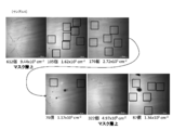
- FIG. 8 is a diagram showing an observation image obtained by observing the surface of a laminated structure of Sample 2 with a multiphoton excitation microscope.
- FIG. 9 is a diagram showing an observation image obtained by observing a cross section of the laminated structure of Sample 4 with a fluorescence microscope.
- FIG. 9 is a diagram showing an observation image obtained by observing the surface of a laminated structure of Sample 4 with a multiphoton excitation microscope.
- FIG. 1 is a flowchart illustrating a method for manufacturing a nitride semiconductor substrate according to the present embodiment.
- 2A to 2C and 4A to 5B are schematic sectional views showing a part of the method for manufacturing a nitride semiconductor substrate according to the present embodiment.
- FIG. 3 is a schematic perspective view showing a part of the method for manufacturing a nitride semiconductor substrate according to the present embodiment.
- FIG. 3 corresponds to a perspective view at the time of FIG. 2B and shows a part of the first layer 30 grown on the base substrate 10.
- a thin solid line indicates a crystal plane during growth
- FIGS. 2C to 5B a dotted line indicates dislocation.
- the method for manufacturing a nitride semiconductor substrate according to the present embodiment includes, for example, a base substrate preparing step S100, a mask layer forming step S180, a first step S200, a second step S300, and a slice. It has a step S400 and a polishing step S500.
- base substrate preparation step S100 base substrate preparation step
- base substrate 10 made of a single crystal of a group III nitride semiconductor is prepared.
- GaN gallium nitride
- a ⁇ 0001> axis (for example, [0001] axis) is referred to as “c-axis” and a (0001) plane is referred to as “c-plane”.
- the (0001) plane may be referred to as “+ c plane (group III element polar plane)”, and the (000-1) plane may be referred to as “ ⁇ c plane (nitrogen (N) polar plane)”.
- the ⁇ 1-100> axis (for example, the [1-100] axis) is referred to as “m-axis”, and the (1-100) plane is referred to as “m-plane”.
- the m-axis may be described as a ⁇ 10-10> axis.
- the ⁇ 11-20> axis (for example, the [11-20] axis) is referred to as “a-axis”, and the (11-20) plane is referred to as “a-plane”.
- the base substrate 10 is manufactured by, for example, a VAS (Void-Assisted Separation) method.
- VAS Vaid-Assisted Separation
- the base substrate 10 is manufactured by the following procedure. First, a substrate such as a sapphire substrate is prepared. After preparing the substrate, a first crystal layer made of, for example, gallium nitride (GaN) is grown on the substrate by, for example, a metal organic chemical vapor deposition (MOVPE) method. After growing the first crystal layer, a metal layer made of, for example, titanium (Ti) is deposited on the first crystal layer. After the metal layer is deposited, for example, the substrate is heat-treated in an atmosphere containing ammonia gas. Thus, the metal layer is nitrided to form a metal nitride layer having high-density fine holes on the surface.
- a substrate such as a sapphire substrate is prepared.
- a first crystal layer made of, for example, gallium nitride (GaN) is grown on the substrate by, for example, a metal organic chemical vapor deposition (MOVPE) method. After growing the first crystal layer, a metal layer made
- a part of the first crystal layer is etched through the holes of the metal nitride layer, and high-density voids are formed in the first crystal layer. Thereby, a void-containing first crystal layer is formed.
- a second crystal layer made of, for example, GaN is grown on the void-containing first crystal layer and the metal nitride layer by, for example, hydride vapor phase epitaxy (HVPE). Let it.
- HVPE hydride vapor phase epitaxy
- the second crystal layer spontaneously separates from the substrate at the boundary between the void-containing first crystal layer and the metal nitride layer.
- the second crystal layer is sliced and polished.
- base substrate 10 made of GaN single crystal is obtained.
- the diameter of the base substrate 10 is, for example, 2 inches or more.
- the thickness of the base substrate 10 is, for example, not less than 300 ⁇ m and not more than 1 mm.
- the main surface 10s of the base substrate 10 has, for example, a main surface (base surface) 10s to be an epitaxial growth surface.
- the crystal plane having a low index closest to the main surface 10s is, for example, a c-plane (+ c-plane).
- a predetermined off-angle may be given to the main surface 10s of the GaN crystal constituting the base substrate 10.
- the “off angle” refers to an angle formed by the c-axis with respect to a normal line of the main surface 10s.
- the magnitude of the off-angle on the main surface 10s of the base substrate 10 is, for example, more than 0 ° and 1 ° or less.
- the magnitude and direction of the off-angle can be adjusted by, for example, the magnitude and direction of the off-angle of the substrate for crystal growth used in the above-described VAS method, and the slice angle and slice direction at the time of slicing. .
- the dislocation density on the main surface 10s of the base substrate 10 is low.
- the dislocation density on main surface 10s of base substrate 10 is, for example, not less than 3 ⁇ 10 6 cm ⁇ 2 and less than 1 ⁇ 10 7 cm ⁇ 2 .
- the mask layer 20 is formed on the base substrate 10 by, for example, a sputtering method.
- the mask layer 20 is, for example, a silicon oxide (SiO 2 ) layer or a silicon nitride (SiN) layer.
- the thickness of the mask layer 20 is not less than 300 nm and not more than 2 ⁇ m.
- the mask layer 20 is patterned by photolithography.
- a mask layer 20 having a plurality of predetermined openings 20a is formed.
- the mask layer 20 having the plurality of openings 20a it is possible to induce three-dimensional growth of a single crystal of GaN in a first step S200 described later.
- the openings 20a of the mask layer 20 are formed, for example, in a stripe shape extending along any one of a direction along the m-axis and a direction along the a-axis.
- the case where the opening 20a of the mask layer 20 has a "striped shape extending along any one of the direction along the m-axis and the direction along the a-axis" refers to a plan view.
- the direction in which the stripe-shaped openings 20a extend is a direction completely along the direction along the m-axis or the direction along the a-axis
- the direction along the m-axis or the a-axis This includes a case in which the direction is slightly inclined with respect to the direction along.
- At least one unit opening constituting the striped opening 20a the length of one of the directions along the m-axis or the direction along the a-axis is set to the length of the other direction component. You may think that it is longer than that.
- At least one unit opening constituting the stripe-shaped opening 20 a does not necessarily extend from one end to the other end of the main surface 10 s of the base substrate 10.
- the openings 20a of the mask layer 20 are formed, for example, in a stripe shape extending in the direction along the a-axis.
- each width w of the stripe-shaped mask layer 20 is, for example, 1 ⁇ m or more and 100 ⁇ m or less, preferably 5 ⁇ m or more and 30 ⁇ m or less.
- the width w of the mask layer 20 is set to 1 ⁇ m or more, disconnection of the mask layer 20 can be suppressed, and the yield of patterning can be improved. Further, by setting the width w of the mask layer 20 to 5 ⁇ m or more, the yield of patterning can be further improved.
- the width w of the mask layer 20 by setting the width w of the mask layer 20 to 100 ⁇ m or less, occurrence of abnormal crystal nuclei on the mask layer 20 can be suppressed in the first step S200 described later. Further, by setting the width w of the mask layer 20 to 30 ⁇ m or less, it is possible to stably suppress the occurrence of abnormal crystal nuclei on the mask layer 20 in the first step S200 described later.
- the pitch p of each of the stripe-shaped mask layers 20 affects, for example, a distance in which dislocations are bent and propagated in a first step S200 and a second step S300, which will be described later. This affects the area of the low dislocation density region on the surface 1s.
- the pitch p of the mask layer 20 is large, it has been difficult to stably grow the GaN crystal.
- the present embodiment by using a substrate manufactured by the VAS method as the base substrate 10, Even if the pitch p of 20 is wide, the first layer 30 described later can be grown stably.
- the pitch p of each of the mask layers 20 is, for example, 800 ⁇ m or more, preferably 1 mm or more. If the pitch p of the mask layer 20 is less than 800 ⁇ m, a high dislocation density region is formed above the mask layer 20, so that when the semiconductor device is cut out from the nitride semiconductor substrate 1, the high dislocation density region is formed in the semiconductor device. May be included. On the other hand, by setting the pitch p of the mask layer 20 to 800 ⁇ m or more, the high dislocation density region is prevented from being included in the semiconductor device, and the semiconductor device can be cut out mainly from the low dislocation density region. .
- the pitch p of the mask layer 20 is 1 mm or more
- the chip size of a semiconductor device such as a high-power light emitting diode (LED) is 600 ⁇ m or more and 1 mm or less.
- the semiconductor device can be stably cut out from the low dislocation density region.
- each pitch p of the mask layer 20 is preferably, for example, 10 mm or less.
- a plurality of concave portions 30p formed by being surrounded by the inclined interface 30i other than the c-plane are further formed on the top surface 30u of the single crystal, and as the position goes over the main surface 10s of the base substrate 10, the inclined interface becomes 30i is gradually enlarged, and the c-plane 30c is gradually reduced. This causes the c-plane 30c to disappear from the top surface 30u. As a result, the first layer 30 whose surface is constituted only by the inclined interface 30i is grown.
- the first layer 30 is three-dimensionally grown so as to intentionally roughen the main surface 10s of the base substrate 10. Note that, even if such a growth mode is formed, the first layer 30 is grown as a single crystal as described above. In this respect, the first layer 30 is different from a so-called low-temperature growth buffer layer formed as amorphous or polycrystalline on a heterogeneous substrate such as sapphire before epitaxially growing a group III nitride semiconductor on the heterogeneous substrate. is there.
- the first layer 30 for example, a layer made of the same group III nitride semiconductor as the group III nitride semiconductor constituting the base substrate 10 is epitaxially grown.
- the GaN layer is epitaxially grown as the first layer 30 by heating the base substrate 10 by HVPE and supplying a GaCl gas and an NH 3 gas to the heated base substrate 10. .
- the first layer 30 is grown under predetermined first growth conditions in order to express the above-described growth process.
- FIG. 6A is a schematic cross-sectional view showing a growth process under reference growth conditions in which each of the inclined interface and the c-plane does not expand or contract.
- a thick solid line indicates the surface of the first layer 30 per unit time.
- the inclined interface 30i shown in FIG. 6A is assumed to be the inclined interface most inclined with respect to the c-plane 30c.
- the growth rate of the c-plane 30c of the first layer 30 is G c0
- the growth rate of the inclined interface 30i of the first layer 30 is Gi
- the growth rate of the first layer 30 is G i .
- the angle between the c-plane 30c and the inclined interface 30i is defined as ⁇ .
- FIG. 6B is a schematic cross-sectional view showing a growth process under the first growth condition in which the inclined interface is enlarged and the c-plane is reduced.
- the thick solid line indicates the surface of the first layer 30 per unit time.
- the inclined interface 30i shown in FIG. 6B is also the inclined interface that is the most inclined with respect to the c-plane 30c.
- the growth rate of the c-plane 30c of the first layer 30 and G c1 the progression rate of the locus of the intersection between the inclined surface 30i and the c-plane 30c of the first layer 30 and R 1.
- the smaller one is ⁇ R1 .
- the traveling rate R 1 of the locus of the intersection between the inclined surface 30i and the c-plane 30c is represented by the following formula (b).
- R 1 G i / cos ⁇ ′ (b)
- the growth rate G c1 of c plane 30c of the first layer 30 is expressed by the following equation (c).
- G c1 R 1 sin ⁇ R1 (c)
- G c1 G i sin ⁇ R1 / cos ( ⁇ + 90 ⁇ R1 ) (d)
- the first growth condition in which the inclined interface 30i is enlarged and the c-plane 30c is reduced preferably satisfies the following expression (1) by the expression (d) and ⁇ R1 ⁇ 90 °.
- G i is the growth rate of the inclined surface 30i of the most inclined relative to the c plane 30c
- theta includes an inclined surface 30i of the most inclined relative to the c plane 30c
- the c-plane 30c Angle is the first growth condition in which the inclined interface 30i is enlarged and the c-plane 30c is reduced.
- G c1 under the first growth condition is preferably larger than G c0 under the reference growth condition.
- the expression (1) can be derived by substituting the expression (a) into G c1 > G c0 .
- the growth condition for expanding the inclined interface 30i that is the most inclined with respect to the c-plane 30c is the strictest condition, if the first growth condition satisfies the expression (1), the other inclined interface 30i is also enlarged. Becomes possible. Further, as G c1 becomes larger with respect to G i / cos ⁇ , the inclined interface 30i is enlarged, and the c-plane 30c is easily reduced.
- the first growth condition preferably satisfies, for example, the following expression (1 ′).
- the growth temperature in the first step S200 is set lower than the growth temperature in the second step S300 described later.
- the growth temperature in the first step S200 is, for example, 980 ° C. or higher and 1020 ° C. or lower, preferably 1000 ° C. or higher and 1020 ° C. or lower.
- the ratio of the partial pressure of the flow rate of the NH 3 gas as the nitriding gas to the partial pressure of the GaCl gas as the group III source gas in the first step S200 may be larger than the V / III ratio in the second step S300 described later.
- the V / III ratio in the first step S200 is, for example, 2 or more and 20 or less, preferably 2 or more and 15 or less.
- At least one of the growth temperature and the V / III ratio is adjusted within the above range so as to satisfy the expression (1).
- Other conditions of the first growth condition of the present embodiment are, for example, as follows. Growth pressure: 90 to 105 kPa, preferably 90 to 95 kPa GaCl gas partial pressure: 1.5 to 15 kPa N 2 gas flow rate / H 2 gas flow rate: 0 to 1
- the first step S200 of the present embodiment is classified into two steps based on, for example, the growing state of the first layer 30.
- the first step S200 of the present embodiment includes, for example, an inclined interface enlarging step S220 and an inclined interface maintaining step S240.
- the first layer 30 has, for example, the inclined interface enlarging layer 32 and the inclined interface maintaining layer 34.
- the c-plane 30c is directly above the opening 20a of the mask layer 20 in the direction normal to the main surface 10s of the base substrate 10 (the direction along the c-axis).
- the inclined interface enlarged layer 32 grows.
- crystal growth is suppressed.
- the inclined interface 30i other than the c-plane is exposed at the position of the inclined interface enlarged layer 32 on the mask layer 20 side.
- the pair of inclined interfaces 30i are formed so as to face each other with one mask layer 20 interposed therebetween.
- the “inclined interface 30i” means a growth interface inclined with respect to the c-plane 30c, and is represented by a low-index facet other than the c-plane, a high-index facet other than the c-plane, or a plane index. Includes slopes that cannot be used.
- the facets other than the c-plane are, for example, ⁇ 11-2m ⁇ and ⁇ 1-10n ⁇ .
- m and n are integers other than 0.
- the inclined interface 30i As described above, by exposing the inclined interface 30i at a position of the inclined interface enlarging layer 32 on the mask layer 20 side, the pair of inclined interfaces 30i and the c-plane 30c sandwiched between the pair of inclined interfaces 30i are exposed.
- the inclined interface enlargement layer 32 having the surface 30u is formed.
- the inclined interface enlarged layer 32 by gradually growing the inclined interface enlarged layer 32 under the first growth condition, as shown in FIG. 2B and FIG. 3, the top surface of the inclined interface enlarged layer 32 exposing the c-plane 30c.
- a plurality of recesses 30p constituted by inclined interfaces 30i other than the c-plane are generated.
- the plurality of concave portions 30p constituted by the inclined interfaces 30i other than the c-plane are randomly formed on the top surface 30u.
- the inclined interface enlarged layer 32 in which the c-plane 30c and the inclined interface 30i other than the c-plane are mixed on the surface is formed.
- the inclined interface 30i formed on the top surface 30u of the inclined interface enlarged layer 32 exposing the c-plane 30c is similar to the inclined interface 30i formed on the mask layer 20 described above. Means a growth interface inclined with respect to.
- a plurality of recesses 30p constituted by the inclined interface 30i other than the c-plane are formed on the top surface 30u of the inclined interface enlarged layer 32, and the c-plane 30c is eliminated, as shown in FIG. 2 (c).
- a plurality of valleys 30v and a plurality of peaks 30t are formed on the surface of the inclined interface enlargement layer 32.
- Each of the plurality of valleys 30v is an inflection point convex downward on the surface of the inclined interface enlarged layer 320, and is formed above a position where each of the inclined interfaces 30i other than the c-plane occurs.
- each of the plurality of tops 30t is an inflection point that is upwardly convex on the surface of the inclined interface enlarged layer 320, and is c-plane across a pair of inclined interfaces 30i that are enlarged in opposite directions.
- 30c is formed at or above the (finally) lost and terminated position.
- the valleys 30v and the tops 30t are formed alternately in a direction along the main surface 10s of the base substrate 10.
- the plurality of valleys 30v include a valley formed by a pair of inclined interfaces 30i above the mask layer 20.
- a plurality of recesses 30p formed by the inclined interface 30i other than the c-plane are formed on the top surface 30u of the inclined interface enlarged layer 32 grown above the opening 20a of the mask layer 20.
- a plurality of troughs 30v and a plurality of tops 30t are formed above the openings 20a of the mask layer 20.
- at least one valley 30v and a plurality of tops 30t are formed above each one of the plurality of openings 20a of the mask layer 20.
- the height from the main surface 10s to the top 30t of the base substrate 10 is made lower than in the case where a large substantially triangular prism-shaped three-dimensional growth layer having only one top is formed above the opening of the mask. Can be. As a result, the surface of the second layer 40 described later can be quickly mirror-finished.
- the c-plane 30c is used as the growth surface without forming the inclined interface 30i immediately above the opening 20a of the mask layer 20. Is grown to a predetermined thickness, and then an inclined interface 30i other than the c-plane is formed on the surface of the enlarged inclined interface layer 32. As a result, the plurality of valleys 30v formed above the openings 20a of the mask layer 20 are formed at positions separated upward from the main surface 10s of the base substrate 10.
- the dislocation propagates by bending as follows. Specifically, as shown in FIG. 2C, a part of the plurality of dislocations extending in the direction along the c-axis in the base substrate 10 is blocked by the mask layer 20 and tilted. Propagation to the interface expansion layer 32 is suppressed. On the other hand, the other part of the plurality of dislocations extending in the direction along the c-axis in the base substrate 10 has the other part of the inclined interface enlarged layer 32 from the base substrate 10 via the opening 20 a of the mask layer 20. It propagates in the direction along the c-axis.
- dislocations propagate from the base substrate 10 in a direction along the c-axis of the inclined interface enlarged layer 32.
- the dislocation is substantially perpendicular to the inclined interface 30i at the position where the inclined interface 30i is exposed. It bends and propagates in the direction. That is, the dislocation propagates while bending in a direction inclined with respect to the c-axis.
- an average distance L (also referred to as an “average distance between nearest top parts”) L between the base substrates 10 in a direction along the main surface 10s is, for example, more than 100 ⁇ m.
- the average distance L between the closest apexes is 100 ⁇ m or less, such as when a fine hexagonal pyramid-shaped crystal nucleus is formed on the main surface 10s of the base substrate 10 from the initial stage of the inclined interface enlarging step S220, the inclination In the steps subsequent to the interface enlarging step S220, the distance over which the dislocations bend and propagate is reduced. For this reason, dislocations cannot be sufficiently collected above the approximate center of the pair of top portions 30t in the inclined interface enlarged layer 32. As a result, the dislocation density on the surface of the second layer 40 described later may not be sufficiently reduced.
- the distance at which the dislocation bends and propagates in the steps after the inclined interface enlarging step S220 is at least more than 50 ⁇ m. be able to.
- dislocations can be sufficiently collected above substantially the center between the pair of top portions 30t in the inclined interface enlarged layer 32.
- the dislocation density on the surface of the second layer 40 described below can be sufficiently reduced.
- the average distance L between the closest tops especially above the opening 20 a of the mask layer 20 is more than 100 ⁇ m.
- the average distance L between the closest tops is set to less than 800 ⁇ m. If the average distance L between the adjacent top portions is 800 ⁇ m or more, the height from the main surface 10s of the base substrate 10 to the valley portion 30v of the inclined interface enlarged layer 32 to the top portion 30t becomes excessively high. Therefore, in a second step S300 described later, the thickness until the second layer 40 is mirror-finished increases.
- the average distance L between the closest apexes is set to less than 800 ⁇ m, the height from the main surface 10s of the base substrate 10 to the valley 30v of the inclined interface enlarged layer 32 to the top 30t is reduced. can do. Thereby, in the second step S300 described later, the second layer 40 can be mirror-finished quickly.
- the first c-plane growth region 60 grown with the c-plane 30c as the growth plane and the inclined interface 30i other than the c-plane are formed in the inclined interface expansion layer 320 based on the difference in the growth plane during the growth process.
- An inclined interface growth region 70 (a gray portion in the figure) grown as a growth surface is formed.
- a valley 60a is formed at a position where the inclined interface 30i has occurred, and a crest 60b is formed at a position where the c-plane 30c has disappeared.
- a pair of inclined portions 60i are formed on both sides of the crest 60b as trajectories of intersections between the c-plane 30c and the inclined interface 30i.
- the angle ⁇ formed by the pair of inclined portions 60i is set to, for example, 70 ° or less by satisfying Expression (1) under the first growth condition.
- the c-plane 30c may reappear on a part of the surface of the inclined interface maintaining layer 34, but the area ratio of the inclined interface growth region 70 in the creep section along the main surface 10s of the base substrate 10 is 80%. %, It is preferable to mainly expose the inclined interface 30i on the surface of the inclined interface maintaining layer 34. The higher the proportion of the area occupied by the inclined interface growth region 70 in the creeping cross section, the better, and preferably 100%.
- the growth condition in the inclined interface maintaining step S240 is maintained under the above-described first growth condition, similarly to the inclined interface expanding step S220.
- the inclined interface maintaining layer 34 can be grown using only the inclined interface 30i as a growth surface.
- the inclined interface maintaining layer 34 grows with the inclined interface 30i as a growth surface, so that the entire inclined interface maintaining layer 34 becomes a part of the inclined interface growing region 70.
- the first layer 30 having the inclined interface enlarged layer 32 and the inclined interface maintaining layer 34 is formed.
- the height from the main surface 10s of the base substrate 10 to the top 30t of the first layer 30 (the maximum height in the thickness direction of the first layer 30) is, for example, more than 100 ⁇ m1. 0.5 mm or less.
- the inclined interface 40i is gradually reduced and the c-plane 40c is gradually expanded toward the upper side of the main surface 10s of the base substrate 10.
- the inclined interface 30i formed on the surface of the first layer 30 is eliminated.
- a second layer (planarization layer) 40 having a mirror-finished surface is grown.
- the “mirror surface” refers to a surface having a maximum height difference between the surface irregularities and the wavelength of visible light or less.
- the second layer 40 for example, a layer mainly composed of the same group III nitride semiconductor as the group III nitride semiconductor constituting the first layer 30 is epitaxially grown.
- a GaCl gas, an NH 3 gas and a dichlorosilane (SiH 2 Cl 2 ) gas as an n-type dopant gas are supplied to the base substrate 10 heated to a predetermined growth temperature.
- a silicon (Si) -doped GaN layer is epitaxially grown.
- GeCl 4 gas or the like may be supplied as the n-type dopant gas instead of SiH 2 Cl 2 gas.
- the second layer 40 is grown under, for example, predetermined second growth conditions in order to express the above-described growth process.
- FIG. 7 is a schematic cross-sectional view showing a growth process under the second growth condition in which the inclined interface is reduced and the c-plane is enlarged.
- FIG. 7 shows a process in which the second layer 40 grows on the first layer 30 where the inclined interface 30i that is the most inclined with respect to the c-plane 30c is exposed.
- a thick solid line indicates the surface of the second layer 40 per unit time.
- the growth rate of the c-plane 40 c of the second layer 40 is G c2
- the growth rate of the inclined interface 40 i of the second layer 40 is G i
- the inclination rate of the second layer 40 is G i. the progress rate of locus of intersection of the surface 40i and the c-plane 40c and R 2.
- the smaller one is ⁇ R2 .
- the traveling rate R 2 of the locus of the intersection between the inclined surface 40i and the c-plane 40c is represented by the following formula (e).
- R 2 G i / cos ⁇ ”(e)
- the growth rate G c2 c-plane 40c of the second layer 40 is expressed by the following equation (f).
- G c2 R 2 sin ⁇ R2 (f)
- G c2 G i sin ⁇ R2 / cos ( ⁇ + ⁇ R2 ⁇ 90) (g)
- the second growth condition in which the inclined interface 40i is reduced and the c-plane 40c is expanded preferably satisfies the following expression (2) by using expression (g) and ⁇ R2 ⁇ 90 °.
- G i is the growth rate of the inclined surface 40i of the most inclined relative to the c plane 40c
- theta includes an inclined surface 40i of the most inclined relative to the c plane 40c
- the c-plane 40c Angle is the second growth condition in which the inclined interface 40i is reduced and the c-plane 40c is expanded.
- equation (2) can be derived by substituting equation (a) into G c2 ⁇ G c0 .
- the growth condition for reducing the inclined interface 40i that is the most inclined with respect to the c-plane 40c is the strictest condition, if the second growth condition satisfies the expression (2), the other inclined interface 40i is also reduced. Becomes possible.
- the second growth condition preferably satisfies the following expression (2 ′).
- the growth temperature in the second step S300 is, for example, higher than the growth temperature in the first step S200.
- the growth temperature in the second step S300 is, for example, not less than 990 ° C. and not more than 1120 ° C., preferably not less than 1020 ° C. and not more than 1100 ° C.
- the V / III ratio in the second step S300 may be adjusted.
- the V / III ratio in the second step S300 may be smaller than the V / III ratio in the first step S200.
- the V / III ratio in the second step S300 is, for example, 1 or more and 10 or less, preferably 1 or more and 5 or less.
- the second growth condition at least one of the growth temperature and the V / III ratio is adjusted within the above range so as to satisfy the expression (2).
- Other conditions of the second growth conditions of the present embodiment are, for example, as follows. Growth pressure: 90 to 105 kPa, preferably 90 to 95 kPa GaCl gas partial pressure: 1.5 to 15 kPa N 2 gas flow rate / H 2 gas flow rate: 1 to 20
- the second step S300 of the present embodiment is classified into two steps based on, for example, the form in which the second layer 40 is growing.
- the second step S300 of the present embodiment includes, for example, a c-plane enlargement step S320 and a main growth step S340.
- the second layer 40 has, for example, the c-plane expansion layer 42 and the main growth layer 44.
- the c-plane 40c is enlarged and the inclined interface 40i other than the c-plane is reduced as it goes above the first layer 30.
- the c-plane expanding layer 42 moves from the inclined interface 30i of the inclined interface maintaining layer 34 to a direction along the direction perpendicular to the c-axis with the inclined interface 40i as a growth surface. (Ie, creeping or lateral).
- the c-plane expanding layer 42 grows in the lateral direction, the c-plane 40c of the c-plane expanding layer 42 starts to be exposed again above the top 30t of the inclined interface maintaining layer 34.
- the c-plane enlarged layer 42 in which the c-plane 40c and the inclined interface 40i other than the c-plane are mixed on the surface is formed.
- the inclined interface 40i of the c-plane enlarged layer 42 completely disappears, and the recess 30p formed by the plurality of inclined interfaces 30i is completely embedded in the surface of the first layer 30. It is. Thereby, the surface of the c-plane expansion layer 42 becomes a mirror surface (flat surface) composed of only the c-plane 40c.
- dislocation density can be reduced by locally collecting dislocations.
- dislocations that have been bent and propagated in the first layer 30 in a direction inclined with respect to the c-axis continue to propagate in the same direction in the c-plane enlarged layer 42.
- dislocations are locally collected at the junction of the adjacent inclined interfaces 40i above the approximate center between the pair of top portions 30t in the c-plane enlarged layer 42.
- Dislocations having mutually opposite Burgers vectors among a plurality of dislocations collected at the meeting portion of the adjacent inclined interface 40i in the c-plane expansion layer 42 disappear during the meeting.
- some of the dislocations collected at the meeting portion of the adjacent inclined interface 40i form a loop and may propagate in the direction along the c-axis (that is, the surface side of the c-plane enlarged layer 42). Is suppressed.
- the other portion of the plurality of dislocations collected at the meeting portion of the adjacent inclined interface 40i in the c-plane expansion layer 42 has its propagation direction changed from the direction inclined to the c-axis to the direction along the c-axis. It is changed again and propagates to the surface side of the second layer 40.
- the dislocation density on the surface of the second layer 40 is reduced. Can be reduced.
- a low dislocation density region can be formed above a portion of the second layer 40 where the dislocations propagate in a direction inclined with respect to the c-axis.
- the c-plane 40c gradually expands, so that a second c-plane growth region 80 described later, which has grown with the c-plane 40c as a growth surface, goes upward in the thickness direction. Therefore, it is formed while gradually expanding.
- the inclined interface 40i is gradually reduced, so that the inclined interface growth region 70 is gradually reduced as going upward in the thickness direction, and terminates at a predetermined position in the thickness direction.
- a valley 70a of the inclined interface growth region 70 is formed at a position where the c-plane 40c is generated again in a sectional view.
- a peak 70b of the inclined interface growth region 70 is formed at a position where the inclined interface 40i has disappeared in a cross-sectional view.
- the height of the c-plane enlargement layer 42 in the thickness direction is For example, the height is equal to or more than the height from the valley 30v to the top 30t of the inclined interface maintaining layer 34.
- the growth conditions in the main growth step S340 are maintained under the above-described second growth conditions, similarly to the c-plane enlargement step S320.
- the main growth layer 44 can be grown in a step flow with the c-plane 40c as a growth surface.
- the entire main growth layer 44 is in contact with a second c-plane growth region 80 described later. Become.
- the thickness of the main growth layer 44 is, for example, 300 ⁇ m or more and 10 mm or less.
- the thickness of the main growth layer 44 is set to 300 ⁇ m or more, at least one or more substrates 1 can be sliced from the main growth layer 44 in a slicing step S400 described below.
- the thickness of the main growth layer 44 is set to 10 mm, the final thickness is set to 650 ⁇ m, and when the substrate 1 having a thickness of 700 ⁇ m is sliced from the main growth layer 44, the kerf loss may be about 200 ⁇ m. , At least ten substrates 1 can be obtained.
- the second layer 40 having the c-plane enlarged layer 42 and the main growth layer 44 is formed.
- the laminated structure 2 of the present embodiment is formed.
- the main growth layer 44 is sliced by a wire saw along a cut surface substantially parallel to the surface of the main growth layer 44.
- at least one nitride semiconductor substrate 1 (hereinafter, also referred to as substrate 1) as an as-sliced substrate is formed.
- the thickness of the substrate 1 is, for example, not less than 300 ⁇ m and not more than 700 ⁇ m.
- both surfaces of the substrate 1 are polished by a polishing apparatus.
- the final thickness of the substrate 1 is, for example, 250 ⁇ m or more and 650 ⁇ m or less.
- the substrate 1 according to the present embodiment is manufactured by the above steps S100 to S500.
- semiconductor laminate manufacturing process and semiconductor device manufacturing process After the substrate 1 is manufactured, for example, a semiconductor functional layer made of a group III nitride semiconductor is epitaxially grown on the substrate 1 to produce a semiconductor laminate. After the semiconductor laminate is manufactured, electrodes and the like are formed using the semiconductor laminate, the semiconductor laminate is diced, and chips of a predetermined size are cut out. Thus, a semiconductor device is manufactured.
- the laminated structure 2 of the present embodiment has, for example, a base substrate 10, a mask layer 20, a first layer 30, and a second layer 40.
- the mask layer 20 is provided on the main surface 10s of the base substrate 10 and has a predetermined opening 20a.
- a plurality of openings 20a of the mask layer 20 are provided, for example, in a stripe shape.
- Each pitch p of the mask layers 20 is, for example, 800 ⁇ m or more.
- the first layer 30 is grown on the main surface 10 s of the underlying substrate 10 via the opening 20 a of the mask layer 20, for example.
- the first layer 30 is formed, for example, by forming a plurality of recesses 30p constituted by inclined interfaces 30i other than the c-plane on the top surface 30u of the single crystal of a group III nitride semiconductor, and eliminating the c-plane 30c. It has a plurality of troughs 30v and a plurality of tops 30t.
- the first layer 30 has, for example, a plurality of troughs 30v and a plurality of tops 30t above the opening 20a of the mask layer 20.
- the first layer 30 has, for example, at least one valley portion 30v and a plurality of top portions 30t above each one of the plurality of openings 20a of the mask layer 20.
- the average distance L between closest tops is, for example, more than 100 ⁇ m.
- the first layer 30 includes, for example, a first c-plane growth region (first low oxygen concentration region) 60 and an inclined interface growth region (high oxygen concentration region) 70 based on a difference in growth surface during the growth process. ,have.
- the first c-plane growth region 60 is a region grown with the c-plane 30c as a growth surface.
- the first c-plane growth region 60 has, for example, a plurality of valleys 60a and a plurality of peaks 60b in a cross-sectional view.
- each of the valleys 60a and the peaks 60b means a part of the shape observed based on the difference in emission intensity when the cross section of the laminated structure 2 is observed with a fluorescence microscope or the like, and the first layer It does not mean a part of the shape of the outermost surface generated during the growth of No. 30.
- Each of the plurality of valleys 60a is a point of inflection projecting downward in the first c-plane growth region 60 in a cross-sectional view, and is formed at a position where the inclined interface 30i has occurred. At least one of the plurality of valleys 60a is provided at a position separated upward from the main surface 10s of the base substrate 10.
- each of the plurality of crests 60b is a pair of inclined interfaces 30i that are inflection points that are upwardly convex in the first c-plane growth region 60 and that are enlarged in directions opposite to each other in a cross-sectional view.
- the c-plane 30c is formed at a position where the c-plane 30c disappears (finally) and ends.
- the valleys 60a and the peaks 60b are alternately formed in a direction along the main surface 10s of the base substrate 10.
- a pair of peak portions 60b that are closest to each other among the plurality of peak portions 60b with one of the valley portions 60a interposed therebetween are different from each other.
- the average distance apart in the direction along the main surface 10s of the first layer 30 corresponds to the average distance L between the closest tops of the first layer 30, and is, for example, more than 100 ⁇ m.
- the first c-plane growth region 60 has a pair of inclined portions 60i provided on both sides of one of the plurality of peaks 60b as a locus of the intersection of the c-plane 30c and the inclined interface 30i.
- the inclined portion 60i means a part of a shape observed based on a difference in emission intensity when the cross section of the laminated structure 2 is observed with a fluorescence microscope or the like, and occurs during the growth of the first layer 30. It does not mean the outermost inclined interface 30i.
- the angle ⁇ formed by the pair of inclined portions 60i is, for example, 70 ° or less, and preferably 20 ° or more and 65 ° or less. It angle ⁇ of the pair of inclined portions 60i is 70 ° or less, in the first growth condition, on the growth rate G i of the inclined surface 30i of the most inclined relative to the c plane 30c of the first layer 30, This means that the ratio G c1 / G i of the growth rate G c1 of the c-plane 30c of the first layer 30 was high. Thereby, the inclined interface 30i other than the c-plane can be easily generated. As a result, the dislocation can be easily bent at a position where the inclined interface 30i is exposed.
- the angle ⁇ formed by the pair of inclined portions 60i to 70 ° or less a plurality of valleys 30v and a plurality of tops 30t can be easily formed above the openings 20a of the mask layer 20. Further, by setting the angle ⁇ formed by the pair of inclined portions 60i to 65 ° or less, the inclined interface 30i other than the c-plane can be more easily generated, and a plurality of inclined interfaces 30i are formed above the openings 20a of the mask layer 20. The valleys 30v and the plurality of peaks 30t can be more easily generated.
- the angle ⁇ formed by the pair of inclined portions 60i By setting the angle ⁇ formed by the pair of inclined portions 60i to 20 ° or more, the height from the valley portion 30v to the top portion 30t of the first layer 30 is suppressed, and the second layer 40 is mirror-finished. It is possible to suppress an increase in the thickness up to the point at which it is performed.
- the inclined interface growth region 70 is a region grown using the inclined interface 30i other than the c-plane as a growth surface.
- the lower surface of the inclined interface growth region 70 is formed, for example, according to the shape of the first c-plane growth region 60.
- the inclined interface growth region 70 is provided continuously along the main surface of the base substrate 10.
- the oxygen taken into the inclined interface growth region 70 is, for example, oxygen that is unintentionally mixed into the vapor phase growth apparatus or oxygen that is released from a member (a quartz member or the like) constituting the vapor phase growth apparatus. It is.
- the oxygen concentration in the first c-plane growth region 60 is, for example, 5 ⁇ 10 16 cm ⁇ 3 or less, preferably 3 ⁇ 10 16 cm ⁇ 3 or less, and specifically, 2 ⁇ 10 16 cm ⁇ 3. It is as follows.
- the oxygen concentration in the inclined interface growth region 70 is, for example, not less than 9 ⁇ 10 17 cm ⁇ 3 and not more than 5 ⁇ 10 19 cm ⁇ 3 .
- the second layer 40 includes, for example, an inclined interface growth region (high oxygen concentration region) 70 and a second c-plane growth region (second low oxygen concentration region) 80 based on a difference in the growth surface during the growth process.
- an inclined interface growth region (high oxygen concentration region) 70 and a second c-plane growth region (second low oxygen concentration region) 80 based on a difference in the growth surface during the growth process.
- the upper surface of the inclined interface growth region 70 in the second layer 40 has, for example, a plurality of valleys 70a and a plurality of peaks 70b in a cross-sectional view.
- each of the valleys 70a and the ridges 70b means a part of the shape observed based on the difference in emission intensity when the cross section of the laminated structure 2 is observed with a fluorescence microscope or the like, and the second layer It does not mean a part of the shape of the outermost surface generated during the growth of 40.
- the plurality of valleys 70a of the inclined interface growth region 70 are formed at positions where the c-plane 40c occurs again in a cross-sectional view.
- the plurality of valleys 70a of the inclined interface growth region 70 are formed above the plurality of peaks 60b of the first c-plane growth region 60, respectively, in a cross-sectional view.
- the plurality of peaks 70b of the inclined interface growth region 70 are formed at positions where the inclined interface 40i has disappeared and terminated in a cross-sectional view.
- the plurality of peaks 70b of the inclined interface growth region 70 are respectively formed above the plurality of valleys 60a of the first c-plane growth region 60 in a cross-sectional view.
- a surface of the second layer 40 that is substantially parallel to the main surface 10 s of the underlying substrate 10 at the upper end of the inclined interface growth region 70 and a boundary surface 40 b at a position where the inclined interface 40 i has disappeared and terminated in the second layer 40.
- the second c-plane growth region 80 is a region grown using the c-plane 40c as a growth surface. In the second c-plane growth region 80, the uptake of oxygen is suppressed as compared with the inclined interface growth region 70. Therefore, the oxygen concentration in the second c-plane growth region 80 is lower than the oxygen concentration in the inclined interface growth region 70.
- the oxygen concentration in the second c-plane growth region 80 is, for example, 5 ⁇ 10 16 cm ⁇ 3 or less, preferably 3 ⁇ 10 16 cm ⁇ 3 or less.
- dislocations are bent and propagate in a direction substantially perpendicular to the inclined interface 30i at a position where the inclined interface 30i other than the c-plane is exposed.
- the second layer 40 some of the dislocations disappear, and some of the dislocations are suppressed from propagating to the surface side of the c-plane enlarged layer 42. Thereby, the dislocation density on the surface of the second layer 40 is lower than the dislocation density on the main surface 10 s of the base substrate 10.
- the dislocation density on the surface of the second layer 40 is sharply reduced in the thickness direction.
- the dislocation density in the main surface 10s of underlying substrate 10 and N 0, the dislocation density at the interface 40b at a position inclined surface 40i is lost out of the second layer 40 and N.
- the dislocation density in the low dislocation density region (for example, 250 ⁇ m square) on the boundary surface 40b is denoted by N.
- a crystal layer of a group III nitride semiconductor is formed on main surface 10s of base substrate 10 with only the c-plane as a growth surface, the thickness being equal to the thickness from the main surface of base substrate 10 to boundary surface 40b of the present embodiment. (Hereinafter, also referred to as “c-plane limited growth”), the dislocation density on the surface of the crystal layer is assumed to be N ′.
- the dislocation density on the surface of the crystal layer tends to be inversely proportional to the thickness of the crystal layer.
- the reduction rate of the dislocation density determined by N ′ / N 0 was approximately 0.6.
- the reduction ratio of the dislocation density obtained by N / N for example, smaller than reduction rate of the dislocation density obtained by N '/ N 0 in the case of c-plane limited growth.
- the thickness of the boundary surface 40b at the position where the inclined interface 40i has disappeared in the second layer 40 from the main surface 10s of the base substrate 10 is, for example, preferably 1.5 mm or less, preferably. Is 1.2 mm or less.
- the reduction rate of the dislocation density obtained by N / N 0 is, for example, 0.3 or less, preferably 0.23 or less.
- the lower limit of the thickness from the main surface 10s of the base substrate 10 to the boundary surface 40b is not limited since the thinner the better, the better.
- the thickness from the main surface 10s to the boundary surface 40b of the base substrate 10 is For example, it is more than 200 ⁇ m.
- the lower limit of the reduction rate of the dislocation density is not limited because the lower the lower the better, the better.
- the reduction rate of the dislocation density is, for example, 0.01 or more.
- the entire surface of the second layer 40 is constituted by the + c plane, and the first layer 30 and the second layer 40 do not include the polarity reversal sections (inversion domains).
- the laminated structure 2 of the present embodiment is different from the laminated structure formed by the so-called DEEP (Dislocation Elimination by the Epitaxial-growth withinverse-pyramidal Pits) method, that is, located at the center of the pit. This is different from a laminated structure having a polarity reversal section in the core.
- Nitride semiconductor substrate nitride semiconductor free-standing substrate, nitride crystal substrate
- the substrate 1 obtained by slicing the second layer 40 by the above-described manufacturing method is, for example, a free-standing substrate made of a single crystal of a group III nitride semiconductor.
- the substrate 1 is, for example, a GaN free-standing substrate.
- the diameter of the substrate 1 is, for example, 2 inches or more.
- the thickness of the substrate 1 is, for example, not less than 300 ⁇ m and not more than 1 mm.
- the conductivity of the substrate 1 is not particularly limited. However, when a semiconductor device as a vertical Schottky barrier diode (SBD) is manufactured using the substrate 1, the substrate 1 is, for example, n-type.
- the n-type impurity in the substrate 1 is, for example, Si or germanium (Ge), and the concentration of the n-type impurity in the substrate 1 is, for example, not less than 1.0 ⁇ 10 18 cm ⁇ 3 and not more than 1.0 ⁇ 10 20 cm ⁇ 3. .
- the substrate 1 has, for example, a main surface 1s to be an epitaxial growth surface.
- the crystal plane of the low index closest to the main surface 1s is, for example, the c-plane.
- the main surface 1s of the substrate 1 is, for example, mirror-finished, and the root mean square roughness RMS of the main surface 1s of the substrate 1 is, for example, less than 1 nm.
- the impurity concentration in the substrate 1 obtained by the above-described manufacturing method is lower than that of the substrate obtained by the flux method or the ammonothermal method.
- the hydrogen concentration in the substrate 1 is, for example, less than 1 ⁇ 10 17 cm ⁇ 3 , preferably 5 ⁇ 10 16 cm ⁇ 3 or less.
- the substrate 1 is formed by slicing the main growth layer 44 grown with the c-plane 40c as the growth surface, the inclined interface growth with the inclined interface 30i or the inclined interface 40i as the growth surface.
- the region 70 is not included. That is, the entire substrate 1 is formed of a low oxygen concentration region.
- the oxygen concentration in the substrate 1 is, for example, 5 ⁇ 10 16 cm ⁇ 3 or less, preferably 3 ⁇ 10 16 cm ⁇ 3 or less.
- the substrate 1 does not include, for example, a polarity inversion section (inversion domain) as described above.
- dark spot means a point where the emission intensity observed in the observation image of the main surface 50s in the multiphoton excitation microscope or the cathode luminescence image of the main surface 50s is low, and only the dislocation is observed. However, it also includes non-light-emitting centers caused by foreign matter or point defects.
- the “multiphoton excitation microscope” may be called a two-photon excitation fluorescence microscope.
- the substrate 1 is manufactured using the base substrate 10 made of a high-purity GaN single crystal manufactured by the VAS method, the non-emission center due to a foreign substance or a point defect is formed in the substrate 1. Less is. Therefore, 95% or more, and preferably 99% or more, of the dark spots when observing the main surface of the substrate 1 with a multiphoton excitation microscope or the like are dislocations, not non-emission centers due to foreign matter or point defects.
- the dislocation density on the surface of the second layer 40 is lower than the dislocation density on the main surface 10 s of the base substrate 10 by the above-described manufacturing method. Thereby, the dislocation is also reduced on the main surface 1s of the substrate 1 formed by slicing the second layer 40.
- the dislocation density is determined from the dark spot density by observing the main surface 1s of the substrate 1 with a visual field of 250 ⁇ m square using a multiphoton excitation microscope, the dislocation density is 3 ⁇ 10 6 cm ⁇ 2. Does not exist, and a region having a dislocation density of less than 1 ⁇ 10 6 cm ⁇ 2 exists at 69% or more, preferably 80% or more of the main surface 1s.
- FIG. 8 is a schematic diagram showing an observation image when the main surface of the nitride semiconductor substrate according to the present embodiment is observed with a multiphoton excitation microscope.
- the square frame in FIG. 8 indicates a predetermined field of view when the substrate is observed with a multiphoton excitation microscope.
- the substrate 1 has a high dislocation density region 1HD within the main surface 1s due to the dislocations being collected above the mask layer 20 used in the above-described manufacturing method. , A low dislocation density region 1LD.
- the dislocation density of the low dislocation density region 1LD is lower than the dislocation density of the high dislocation density region 1HD.
- the dislocation density of the low dislocation density region 1LD in the main surface 1s of the substrate 1 of the present embodiment is, for example, less than 1 ⁇ 10 6 cm ⁇ 2 , and preferably 7 ⁇ 10 5 cm ⁇ 2. Or less, more preferably less than 5.5 ⁇ 10 5 cm ⁇ 2 , and still more preferably 3 ⁇ 10 5 cm ⁇ 2 or less.
- the dislocation density of the high dislocation density region 1HD is slightly lower than that of the base substrate 10, for example, 3 ⁇ 10 6 cm ⁇ 2 or less, preferably 2 ⁇ 10 6 cm ⁇ 2 or less, More preferably, it is 1 ⁇ 10 6 cm ⁇ 2 or less. Note that the dislocation density in the high dislocation density region 1HD is larger than the maximum value of the dislocation density in the low dislocation density region 1LD.
- the position of the high dislocation density region 1HD in plan view corresponds to (overlaps) the position of the mask layer 20 used in the above-described manufacturing method.
- Each of the high dislocation density region 1HD and the low dislocation density region 1LD has, for example, a stripe shape extending along one of the direction along the m-axis and the direction along the a-axis. I have.
- the high dislocation density regions 1HD and the low dislocation density regions 1LD are alternately provided, for example, in the other direction of the direction along the m-axis or the direction along the a-axis.
- each of the high dislocation density region 1HD and the low dislocation density region 1LD has, for example, a stripe shape extending in a direction along the a-axis.
- the high dislocation density regions 1HD and the low dislocation density regions 1LD are provided alternately in a direction along the m-axis perpendicular to the a-axis.
- the pitch P of the high dislocation density region 1HD in the short direction corresponds to the pitch p of the mask layer 20, and is, for example, 800 ⁇ m or more.
- the pitch P of the high dislocation density region 1HD means the distance between the centers of the high dislocation density region 1HD.
- the pitch P of the high dislocation density region 1HD may be considered as a distance from the maximum position of the dislocation density to the adjacent maximum position for every 250 ⁇ m square of the visual field.
- the width W in the short direction of the high dislocation density region 1HD is, for example, 100 ⁇ m or more and 250 ⁇ m or less according to the results of examples described later.
- the proportion of the high dislocation density region 1HD in the main surface 1s of the substrate 1 is determined by W / P ⁇ 100, and is, for example, 31% or less.
- the low dislocation density region 1LD in which the dislocation density on the main surface 1s of the substrate 1 is less than 1 ⁇ 10 6 cm ⁇ 2 is 69% or more, preferably 80% or more of the main surface 1s of the substrate 1. .
- the low dislocation density region 1LD includes, for example, at least a non-dislocation region of 50 ⁇ m square (50 ⁇ m square or more) based on the average distance L between the closest tops in the above-described first step S200. I have.
- non-dislocation regions of 50 ⁇ m square are scattered, for example, over a plurality of low dislocation density regions 1LD.
- the density of the dislocation-free region of 50 ⁇ m square not overlapping for example, 100 pieces / cm 2 or more, preferably 600 / cm 2 or more, more preferably 1200 Pieces / cm 2 or more. If you measure the dislocation-free region in only the low dislocation density region 1LD is in a plurality of low dislocation density region 1LD, the density of the dislocation-free region of 50 ⁇ m square not overlapping, for example, 130 pieces / cm 2 or more, preferably 800 Pcs / cm 2 or more, more preferably 1600 pcs / cm 2 or more.
- the upper limit of the density of the non-overlapping 50 ⁇ m-square non-dislocation region is, for example, 30,000 / cm 2 because the ratio of the visual field including the high dislocation density region is at least 1 /.
- the size of a dislocation-free region is smaller than 50 ⁇ m square, or the density of a 50 ⁇ m-square non-dislocation region is reduced. It becomes lower than 100 pieces / cm 2 .
- the size of the dislocation-free region is smaller than 50 ⁇ m square, or the density of the 50 ⁇ m-square non-dislocation region is 100 / cm 2. Lower than.
- the dislocation density on the main surface 10s of the base substrate 10 used in the above-described manufacturing method is low, when growing the first layer 30 and the second layer 40 on the base substrate 10, a plurality of dislocations are formed. Less binding (mixing). Thereby, in the substrate 1 obtained from the second layer 40, generation of dislocations having a large Burgers vector can be suppressed.
- the Burgers vector is any one of ⁇ 11-20> / 3, ⁇ 0001>, or ⁇ 11-23> / 3.
- the “Burgers vector” here can be measured, for example, by a large-angle convergent electron diffraction (LACBED) method using a transmission electron microscope (TEM).
- LACBED large-angle convergent electron diffraction
- TEM transmission electron microscope
- the dislocation whose Burgers vector is ⁇ 11-20> / 3 is an edge dislocation
- the dislocation whose Burgers vector is ⁇ 0001> is a screw dislocation
- the Burgers vector is ⁇ 11-23> / 3.
- One dislocation is a mixed dislocation in which an edge dislocation and a screw dislocation are mixed.
- the Burgers vector is any one of ⁇ 11-20> / 3, ⁇ 0001>, or ⁇ 11-23> / 3. Is, for example, 50% or more, preferably 70% or more, and more preferably 90% or more. Note that a dislocation having a Burgers vector of 2 ⁇ 11-20> / 3 or ⁇ 11-20> may exist in at least a part of the main surface 50s of the substrate 1.
- an inclined interface 30i other than the c-plane is formed on the surface of the single crystal constituting the first layer 30, so that the inclined interface 30i is exposed at a position where the inclined interface 30i is exposed.
- Dislocations can be bent and propagated in a substantially vertical direction. Thereby, dislocations can be locally collected. By locally collecting dislocations, dislocations having mutually opposite Burgers vectors can be eliminated. Alternatively, the dislocation locally collected forms a loop, so that the dislocation can be suppressed from propagating to the surface of the second layer 40. Thus, the dislocation density on the surface of the second layer 40 can be reduced. As a result, the substrate 1 having a lower dislocation density than the base substrate 10 can be obtained.
- the dislocation propagated from the underlying substrate propagates substantially vertically upward without being bent, and reaches the surface of the second layer. Therefore, the dislocations are not reduced above the portion where the c-plane remains, and a high dislocation density region is formed.
- the c-plane 30c is eliminated from the top surface 30u of the first layer 30, so that the surface of the first layer 30 is only the inclined interface 30i except the c-plane.
- the dislocation propagating from the underlying substrate 10 can be reliably bent over the entire surface of the first layer 30.
- a part of the plurality of dislocations can be easily eliminated or a part of the plurality of dislocations can be hardly propagated to the surface side of the second layer 40.
- the c-plane 30c is easily and reliably eliminated by forming a plurality of recesses 30p formed by the inclined interface 30i other than the c-plane on the top surface 30u of the first layer 30.
- a substantially triangular prism-shaped three-dimensional growth layer having only one top is formed above the opening of the mask without forming a recess on the top surface of the first layer. Then, as described above, it is difficult to eliminate the c-plane during the growth process, and the c-plane may remain at least partially.
- the proportion of the inclined interface 30i occupying the surface of the first layer 30 is increased, and the c-plane 30c is rapidly reduced. Can be done. As a result, even when the pitch of the mask layer 20 is long, the c-plane 30c can be easily and reliably eliminated above the opening 20a of the mask layer 20.
- a plurality of recesses 30p constituted by inclined interfaces 30i other than the c-plane are formed on the top surface 30u of the first layer 30, and the c-plane 30c is eliminated, thereby forming the mask layer 20.
- a plurality of troughs 30v and a plurality of tops 30t can be formed above the opening 20a. In other words, at least one valley 30v and a plurality of tops 30t can be formed above each one of the plurality of openings 20a of the mask layer 20.
- a large substantially triangular prism-shaped three-dimensional growth layer is formed above the opening of the mask.
- the height from the main surface 10s to the top 30t of the base substrate 10 can be made lower than in the case of performing the above.
- the surface of the second layer 40 can be mirror-finished quickly.
- a plurality of valleys 30v and a plurality of peaks 30t are formed at random above the openings 20a of the mask layer 20, so that the bends are formed at positions where the inclined interface 30i other than the c-plane is exposed.
- the dislocations can be randomly dispersed. Thereby, local concentration of dislocations can be suppressed as compared with the case where the mask layer is formed at a narrow pitch. By suppressing the local concentration of dislocations, it is possible to suppress the inclusion of a high dislocation density region in the semiconductor device when cutting the semiconductor device from the substrate 1. As a result, the yield of the semiconductor device can be improved.
- the average distance L between the closest apexes is set to more than 100 ⁇ m, so that the distance at which dislocations bend and propagate is obtained. At least more than 50 ⁇ m.
- the dislocation near the top 30t of the first layer 30 is surely bent particularly by securing a sufficient time for bending the dislocation at a position where the inclined interface 30i other than the c-plane is exposed. Therefore, the propagation of dislocations in the substantially vertical direction from the base substrate 10 toward the surface of the second layer 40 can be suppressed. Thereby, the concentration of dislocations above the top 30t of the first layer 30 can be suppressed.
- the base substrate 10 is a GaN free-standing substrate.
- the base substrate 10 is not limited to the GaN free-standing substrate, and may be, for example, aluminum nitride (AlN), aluminum gallium nitride (AlGaN), or indium nitride.
- InN a group III nitride semiconductor such as indium gallium nitride (InGaN) and aluminum indium gallium nitride (AlInGaN), that is, Al x In y Ga 1-xy N (0 ⁇ x ⁇ 1, 0 ⁇ y ⁇
- AlInGaN aluminum indium gallium nitride
- a self-standing substrate made of a group III nitride semiconductor represented by a composition formula of 1, 0 ⁇ x + y ⁇ 1) may be used.
- the substrate 1 is a GaN free-standing substrate.
- the substrate 1 is not limited to a GaN free-standing substrate. That is, it is a self-supporting substrate made of a group III nitride semiconductor represented by a composition formula of Al x In y Ga 1-xy N (0 ⁇ x ⁇ 1, 0 ⁇ y ⁇ 1, 0 ⁇ x + y ⁇ 1). You may.
- the substrate 1 is n-type.
- the substrate 1 may be p-type or have semi-insulating properties.
- the substrate 1 when manufacturing a semiconductor device as a high electron mobility transistor (HEMT) using the substrate 1, the substrate 1 preferably has semi-insulating properties.
- HEMT high electron mobility transistor
- the base substrate 10 is manufactured by the VAS method in the base substrate preparation step S100 has been described, but a method other than the VAS method may be used as long as the base substrate 10 is manufactured.
- the opening 20a of the mask layer 20 is formed into a stripe shape extending along the direction along the a-axis. May be formed in a stripe shape extending along the direction along the m-axis.
- the first growth condition is as follows.
- the growth conditions other than the growth temperature may be adjusted, or the growth temperature and the growth condition other than the growth temperature may be adjusted in combination.
- the second growth condition is defined as:
- the growth conditions other than the growth temperature may be adjusted, or the growth temperature and the growth condition other than the growth temperature may be adjusted in combination.
- the growth condition in the inclined interface maintaining step S240 is maintained under the first growth condition as in the case of the inclined interface enlarging step S220 has been described.
- the growth condition in the inclined interface maintaining step S240 has been described. May satisfy the first growth condition, the growth condition in the inclined interface maintaining step S240 may be different from the growth condition in the inclined interface expanding step S220.
- the growth condition in the main growth step S340 is maintained under the above-described second growth condition as in the case of the c-plane enlargement step S320 is described. If the second growth condition is satisfied, the growth condition in the main growth step S340 may be different from the growth condition in the c-plane enlargement step S320.
- the main growth layer 44 is sliced using a wire saw in the slicing step S400 has been described.
- an outer peripheral slicer, an inner peripheral slicer, an electric discharge machine, or the like may be used.
- a semiconductor laminate for manufacturing a semiconductor device may be manufactured using the multilayer structure 2 as it is. Specifically, after the multilayer structure 2 is manufactured, in a semiconductor multilayer manufacturing process, a semiconductor functional layer is epitaxially grown on the multilayer structure 2 to manufacture a semiconductor multilayer. After the production of the semiconductor laminate, the back surface side of the laminated structure 2 is polished, and the base substrate 10, the first layer 30, and the c-plane enlarged layer 42 of the laminated structure 2 are removed. Thereby, similarly to the above-described embodiment, a semiconductor laminate having the main growth layer 44 and the semiconductor functional layer is obtained. In this case, the slicing step S400 and the polishing step S500 for obtaining the substrate 1 can be omitted.
- the steps S200 to S500 may be performed again using the substrate 1 as the base substrate 10. Thereby, the substrate 1 with further reduced dislocation density can be obtained. Further, the steps S200 to S500 using the substrate 1 as the base substrate 10 may be defined as one cycle, and the cycle may be repeated a plurality of times. Thereby, the dislocation density of the substrate 1 can be gradually reduced according to the number of times the cycle is repeated.
- the substrate 1 has the high dislocation density region 1HD and the low dislocation density region 1LD has been described.
- the second layer 40 is grown thick, the dislocation occurs during the growth process of the second layer 40. Therefore, there is a possibility that a clear difference between the high dislocation density region 1HD and the low dislocation density region 1LD does not appear on the substrate 1 sliced from the second layer 40.
- Example 2 (Underlying substrate) Same as sample 1. (Mask layer) Same as sample 1. (First layer) Material: GaN Growth method: HVPE method The first growth condition is different from that of sample 1. The first growth condition will be described later. (2nd layer) Same as sample 1.
- sample 3 (Underlying substrate) Same as sample 1. (Mask layer) Same as sample 1. (First layer) Material: GaN Growth method: HVPE method The first growth conditions are different from those of samples 1 and 2. The first growth condition will be described later. (2nd layer) Same as sample 1.
- sample 4 (Underlying substrate) Same as sample 1. (Mask layer) Same as sample 1. (First layer) Material: GaN Growth method: HVPE method The first growth conditions are different from those of samples 1 to 3. The first growth condition will be described later. (2nd layer) Same as sample 1.
- the first growth condition for growing the first layer in Samples 1 to 4 above is to adjust at least one of the growth temperature, the V / III ratio, and the like to adjust the c-plane of the first layer.
- the ratio G c1 / G i of the growth rate G c1 of the c-plane of the first layer to the growth rate G i of the most inclined interface hereinafter, also referred to as “c-plane growth rate ratio G c1 / G i ”).
- the conditions were set such that the order became higher in the order of sample 1 ⁇ sample 2 ⁇ sample 3 ⁇ sample 4.
- the growth temperature in the first step was set to 1030 ° C.
- the V / III ratio was set to 10 so that the first growth condition did not satisfy Expression (1).
- the first growth condition satisfied expression (1), but the growth temperature in the first step was 1023 ° C., and the V / III ratio was 10.
- the growth temperature was 980 ° C. or more and 1020 ° C. or less, and the V / III ratio was 1 or more and 15 or less.
- at least one of the growth temperature and the V / III ratio was adjusted within the above ranges so that the first growth condition satisfied Expression (1).
- the surface (upper surface) of the second layer in the above-described laminated structure was observed.
- the dark spot density (ie, dislocation density) on the surface of the multilayer structure was measured every 250 ⁇ m square of the visual field.
- all the dark spots on these substrates are dislocations by performing measurement while shifting the focus in the thickness direction.
- the ratio of the number of regions (low dislocation density regions) having a dislocation density of less than 1 ⁇ 10 6 cm ⁇ 2 to the total number of measurement regions in a visual field of 250 ⁇ m square was determined.
- FIGS. 9, FIG. 11, FIG. 12, FIG. 14, and FIG. 16 are views showing observation images obtained by observing the cross sections of the laminated structures of Samples 1 to 4 with a fluorescence microscope.
- the arrows on the underlying substrate indicate the positions of the mask layers.
- FIGS. 10, 13, 15, and 17 are views showing observation images obtained by observing the surfaces of the laminated structures of Samples 1 to 4 with a multiphoton excitation microscope.
- the thick frame indicates a 50 ⁇ m square dislocation-free region.
- Sample 1 As shown in FIG. 9, in Sample 1, the top of the first layer is not formed above the opening of the mask layer, and the top of the first c-plane growth region of the first layer and the top of the second layer are not formed. The lower part of the 2c plane growth region was connected. It is considered that the c-plane remained during the growth process of the first layer. The width of the c-plane remaining region was about 200 ⁇ m.
- the c-plane growth rate ratio G c1 / G i was lower than that of the other samples under the first growth condition for growing the first layer, and the first growth condition did not satisfy Expression (1). For this reason, the c-plane could not be eliminated during the growth of the first layer. Since the c-plane did not disappear, the dislocation propagated to the surface side of the second layer without bending in the above-described c-plane remaining region. For this reason, a high dislocation density region was formed at a position overlapping with the c-plane remaining region. As a result, it is considered that the ratio of the low dislocation density region to the surface of the multilayer structure was reduced.
- Sample 2 As shown in FIG. 11, in Sample 2, the c-plane disappeared in the first layer, and a substantially triangular prism-shaped first layer having only one top was formed above the opening of the mask layer. The average distance between the most recent abutments was approximately 1 mm. The height from the main surface of the base substrate to the top of the first c-plane growth region is 890 ⁇ m, and the thickness of the boundary surface of the second layer at the position where the inclined interface has disappeared from the main surface of the base substrate (The thickness until the second layer became a mirror surface) was about 1250 ⁇ m.
- a portion where the c-plane of the first layer remains was scattered in a part of the laminated structure.
- the width of the c-plane remaining region was about 20 ⁇ m.
- the c-plane growth rate ratio G c1 / G i was set higher than that of sample 1 under the first growth condition for growing the first layer, and the first growth condition satisfied Expression (1).
- the c-plane could be eliminated. Thereby, the dislocation could be bent at the position where the inclined interface in the first layer was exposed. As a result, a low dislocation density region could be formed over a range almost overlapping with the opening of the mask layer.
- Example 3 As shown in FIG. 14, in Sample 3, the c-plane disappeared in the first layer, and at least one valley and a plurality of peaks were formed above one opening of the mask layer.
- the average value of the angle formed by the pair of inclined portions in the first c-plane growth region was approximately 57.1 °. Further, the average distance between the closest abutments was about 400 ⁇ m. The average distance between the closest tops above the opening of the mask layer was about 125 ⁇ m.
- the height from the main surface of the base substrate to the top of the first c-plane growth region was about 410 ⁇ m. Further, the inclined interface growth region was formed continuously along the main surface of the underlying substrate. The thickness of the boundary surface of the second layer at the position where the inclined interface disappeared from the main surface of the base substrate was about 980 ⁇ m.
- the low dislocation density region of Sample 3 a plurality of non-dislocation regions of 50 ⁇ m square or more were formed. Non-dislocation regions of 50 ⁇ m square were scattered over a plurality of low dislocation density regions.
- the density of non-overlapping 50 ⁇ m-square non-dislocation regions on the entire surface of the multilayer structure was about 4500 / cm 2 .
- the reduction rate of the dislocation density determined by N / N 0 was, for example, 0.17 or less.
- the c-plane growth rate ratio G c1 / G i was higher than that of samples 1 and 2 under the first growth condition for growing the first layer, and the first growth condition satisfied Expression (1).
- a plurality of recesses were formed on the top surface of the first layer, and the c-plane could be easily and reliably eliminated.
- Dislocation was reliably bent at a position where the inclined interface in the first layer was exposed by reliably removing the c-plane.
- a low-dislocation-density region can be formed over the entire area overlapping with the opening of the mask layer, and the ratio of the low-dislocation-density region to the surface of the multilayer structure can be increased to 69% or more. It was confirmed.
- the c-plane growth rate ratio G c1 / G i under the first growth condition was set higher than that of sample 2, so that at least one valley and a plurality of peaks were formed above the opening of the mask layer. And could be formed. Thereby, it was confirmed that the thickness until the second layer was mirror-finished could be reduced.
- the average distance between the closest cusps could be set to more than 100 ⁇ m.
- the dislocation density in the low dislocation density region could be sufficiently reduced.
- the average distance between the adjacent apexes to be more than 100 ⁇ m, a plurality of non-dislocation regions having a size of 50 ⁇ m square or more can be formed in the low-dislocation density region. It was confirmed that it could be scattered.
- the density of non-overlapping 50 ⁇ m-square non-dislocation regions over the entire surface of the multilayer structure could be 1600 / cm 2 or more.
- sample 4 As shown in FIG. 16, in sample 4, the c-plane disappeared in the first layer, and more valleys and peaks were formed above the openings in the mask layer than in sample 3.
- the average value of the angle formed by the pair of inclined portions in the first c-plane growth region was 54.4 °.
- the average distance between the closest abutments was about 260 ⁇ m.
- the average distance between the closest tops above the openings in the mask layer was about 199 ⁇ m.
- the height from the main surface of the base substrate to the top of the first c-plane growth region was about 360 ⁇ m.
- the inclined interface growth region was formed continuously along the main surface of the underlying substrate.
- the thickness of the boundary surface of the second layer at the position where the inclined interface disappeared from the main surface of the underlying substrate was about 1090 ⁇ m.
- Non-dislocation regions of 50 ⁇ m square were formed.
- Non-dislocation regions of 50 ⁇ m square were scattered over a plurality of low dislocation density regions.
- the density of non-overlapping 50 ⁇ m-square non-dislocation regions on the entire surface of the multilayer structure was approximately 5000 / cm 2 .
- the reduction rate of the dislocation density determined by N / N 0 was, for example, 0.17 or less.
- the c-plane growth rate ratio G c1 / G i was higher than that of Samples 1 to 3 under the first growth condition for growing the first layer, and the first growth condition satisfied Expression (1).
- a plurality of recesses were formed on the top surface of the first layer, and the c-plane could be easily and reliably eliminated.
- a low dislocation density region can be formed over the entire area overlapping with the opening of the mask layer, and the ratio of the low dislocation density region to the surface of the multilayer structure is 69% or more. I confirmed that I was able to.
- the c-plane growth rate ratio G c1 / G i under the first growth condition was higher than that of sample 3, so that more valleys and peaks were formed above the opening of the mask layer than in sample 3. could be formed. Thereby, it was confirmed that the thickness until the second layer was mirror-finished could be reduced.
- the growth time of the first step in sample 4 was the same as that of sample 3, if the growth time in the first step is optimized, the thickness until the second layer is mirror-finished can be reduced. It will be possible.
- the average distance between the closest abutments could be set to more than 100 ⁇ m.
- the dislocation density in the low dislocation density region was sufficiently reduced as in the case of Sample 3.
- the average distance between the closest apexes By setting the average distance between the closest apexes to be more than 100 ⁇ m, a plurality of non-dislocation regions of 50 ⁇ m square or more can be formed in the low dislocation density region similarly to the sample 3, It was confirmed that the particles could be scattered over the dislocation density region.
- the density of non-overlapping 50 ⁇ m-square non-dislocation regions over the entire surface of the multilayer structure could be 1600 / cm 2 or more.
- a method for manufacturing a nitride semiconductor substrate using a vapor phase growth method Preparing a base substrate made of a single crystal of a group III nitride semiconductor and having a main surface whose closest low-index crystal plane is a (0001) plane; Forming a mask layer having a plurality of openings on the main surface of the base substrate; A single crystal of a group III nitride semiconductor having a top surface with the (0001) plane exposed between a pair of inclined interfaces other than the (0001) plane is formed on the main surface of the base substrate by the opening of the mask layer.
- G c1 > G i / cos ⁇ (1)
- G c2 ⁇ G i / cos ⁇ (2)
- the growth rate of the (0001) plane of the first layer is G c1
- the growth rate of the (0001) plane of the second layer is G c2
- the angle between the inclined interface and the (0001) plane is ⁇ .
- the first step includes: A step of gradually expanding the inclined interface toward the upper side of the base substrate, and forming an inclined interface enlarged layer; On the inclined interface enlarged layer in which the (0001) plane has disappeared from the surface, over a predetermined thickness while maintaining the state where the surface is constituted only by the inclined interface other than the (0001) plane. Forming a gradient interface maintaining layer; 7.
- the second step includes: Forming a c-plane enlarged layer by reducing an inclined interface other than the (0001) plane while expanding the (0001) plane toward the upper side of the first layer; Forming a main growth layer on the c-plane enlarged layer having a mirror-finished surface over a predetermined thickness with the (0001) plane as a growth surface; 8.
- the main surface has a low dislocation density region where the dislocation density is less than 1 ⁇ 10 6 cm ⁇ 2 and a high dislocation density where the dislocation density is higher than the dislocation density of the low dislocation density region and 3 ⁇ 10 6 cm ⁇ 2 or less.
- dislocation density regions are alternately arranged, A nitride semiconductor substrate in which at least a part of the low dislocation density region has a non-dislocation region of 50 ⁇ m square or more.
- the first low oxygen concentration region further includes a pair of inclined portions provided on both sides of the mountain portion, The laminated structure according to Supplementary Note 15 or 16, wherein an angle formed by the pair of inclined portions is 70 ° or less.
Landscapes
- Chemical & Material Sciences (AREA)
- Crystallography & Structural Chemistry (AREA)
- Engineering & Computer Science (AREA)
- Materials Engineering (AREA)
- Metallurgy (AREA)
- Organic Chemistry (AREA)
- Chemical Kinetics & Catalysis (AREA)
- General Chemical & Material Sciences (AREA)
- Inorganic Chemistry (AREA)
- Crystals, And After-Treatments Of Crystals (AREA)
Abstract
下地基板を準備する工程と、下地基板の主面上に複数の開口部を有するマスク層を形成する工程と、下地基板の主面上に、表面が傾斜界面のみで構成される第1層を成長させる第1工程と、第1層上にIII族窒化物半導体の単結晶をエピタキシャル成長させ、傾斜界面を消失させ、鏡面化された表面を有する第2層を成長させる第2工程と、を有し、第1工程では、単結晶の頂面に複数の凹部を生じさせ、(0001)面を消失させることで、マスク層の複数の開口部のうちそれぞれ1つの開口部の上方に、少なくとも1つの谷部および複数の頂部を形成し、主面に垂直な任意の断面を見たときに、谷部の1つを挟んで複数の頂部のうちで最も接近する一対の頂部同士が主面に沿った方向に離間した平均距離を、100μm超とする。
Description
本発明は、窒化物半導体基板の製造方法、窒化物半導体基板および積層構造体に関する。
III族窒化物半導体の単結晶を成長させる方法として、いわゆるELO(Epitaxial Lateral Overgrowth)法が知られている。ELO法では、例えば、まず、下地基板上に、所定の開口部を有するマスク層を形成する。マスク層を形成したら、下地基板上にマスク層の開口部を介して断面三角形状のファセット構造を成長させる。さらにファセット構造を成長させると、ファセット構造が形成するV字状の溝部が埋め込まれ、平坦な結晶層が得られる。このとき、ファセット構造の成長過程で、転位が屈曲されることで、結晶層の表面に到達する転位が低減される(例えば、特許文献1および2)。
ここで、上述のELO法では、マスク層のピッチを長くすることで、すなわち、開口部の幅を広くすることで、結晶層の表面における転位密度が低減された領域を広くすることができる。
しかしながら、発明者は、マスク層のピッチを長くした場合に、以下のような課題が生じることを見出した。
マスク層のピッチを長くすると、ファセット構造の成長過程で(0001)面を消失させることが困難となり、頂部が尖った断面三角形状のファセット構造を形成することが困難となる。このため、(0001)面が残存したまま、結晶層が成長する。(0001)面が残存すると、転位が屈曲されずに結晶層の表面に伝播してしまう。その結果、結晶層の表面における転位密度が充分に低減されない可能性がある。
また、マスク層のピッチを長くすると、下地基板の主面からファセット構造の頂部までの高さが高くなる。このため、結晶層を平坦化させるまでの時間が長くなる。その結果、結晶層をスライスすることで得られる窒化物半導体基板の生産性が低下する可能性がある。
本発明は、発明者が見出した上述の新規課題に基づくものであり、本発明の目的は、窒化物半導体基板の主面における転位密度を効率よく低減させることにある。
本発明の一態様によれば、
気相成長法を用いた窒化物半導体基板の製造方法であって、
III族窒化物半導体の単結晶からなり、最も近い低指数の結晶面が(0001)面である主面を有する下地基板を準備する工程と、
前記下地基板の前記主面上に、複数の開口部を有するマスク層を形成する工程と、
前記(0001)面以外の一対の傾斜界面で挟まれ前記(0001)面が露出した頂面を有するIII族窒化物半導体の単結晶を前記下地基板の前記主面上に前記マスク層の前記開口部を介してエピタキシャル成長させ、前記(0001)面以外の傾斜界面で構成される複数の凹部を前記頂面に生じさせ、前記下地基板の前記主面の上方に行くにしたがって該傾斜界面を徐々に拡大させ、前記(0001)面を前記頂面から消失させ、表面が前記傾斜界面のみで構成される第1層を成長させる第1工程と、
前記第1層上にIII族窒化物半導体の単結晶をエピタキシャル成長させ、前記傾斜界面を消失させ、鏡面化された表面を有する第2層を成長させる第2工程と、
を有し、
前記第1工程では、
前記単結晶の前記頂面に前記複数の凹部を生じさせ、前記(0001)面を消失させることで、前記マスク層の前記複数の開口部のうちそれぞれ1つの開口部の上方に、少なくとも1つの谷部および複数の頂部を形成し、
前記主面に垂直な任意の断面を見たときに、前記谷部の1つを挟んで前記複数の頂部のうちで最も接近する一対の頂部同士が前記主面に沿った方向に離間した平均距離を、100μm超とする
窒化物半導体基板の製造方法が提供される。
気相成長法を用いた窒化物半導体基板の製造方法であって、
III族窒化物半導体の単結晶からなり、最も近い低指数の結晶面が(0001)面である主面を有する下地基板を準備する工程と、
前記下地基板の前記主面上に、複数の開口部を有するマスク層を形成する工程と、
前記(0001)面以外の一対の傾斜界面で挟まれ前記(0001)面が露出した頂面を有するIII族窒化物半導体の単結晶を前記下地基板の前記主面上に前記マスク層の前記開口部を介してエピタキシャル成長させ、前記(0001)面以外の傾斜界面で構成される複数の凹部を前記頂面に生じさせ、前記下地基板の前記主面の上方に行くにしたがって該傾斜界面を徐々に拡大させ、前記(0001)面を前記頂面から消失させ、表面が前記傾斜界面のみで構成される第1層を成長させる第1工程と、
前記第1層上にIII族窒化物半導体の単結晶をエピタキシャル成長させ、前記傾斜界面を消失させ、鏡面化された表面を有する第2層を成長させる第2工程と、
を有し、
前記第1工程では、
前記単結晶の前記頂面に前記複数の凹部を生じさせ、前記(0001)面を消失させることで、前記マスク層の前記複数の開口部のうちそれぞれ1つの開口部の上方に、少なくとも1つの谷部および複数の頂部を形成し、
前記主面に垂直な任意の断面を見たときに、前記谷部の1つを挟んで前記複数の頂部のうちで最も接近する一対の頂部同士が前記主面に沿った方向に離間した平均距離を、100μm超とする
窒化物半導体基板の製造方法が提供される。
本発明の他の態様によれば、
2インチ以上の直径を有し、最も近い低指数の結晶面が(0001)面である主面を有する窒化物半導体基板であって、
多光子励起顕微鏡により前記窒化物半導体基板の主面を観察して暗点密度から転位密度を求めたときに、
前記主面には、転位密度が1×106cm-2未満である低転位密度領域と、転位密度が前記低転位密度領域の転位密度よりも高く3×106cm-2以下である高転位密度領域とが、交互に配列しており、
前記低転位密度領域の少なくとも一部は、50μm角以上の無転位領域を有する
窒化物半導体基板が提供される。
2インチ以上の直径を有し、最も近い低指数の結晶面が(0001)面である主面を有する窒化物半導体基板であって、
多光子励起顕微鏡により前記窒化物半導体基板の主面を観察して暗点密度から転位密度を求めたときに、
前記主面には、転位密度が1×106cm-2未満である低転位密度領域と、転位密度が前記低転位密度領域の転位密度よりも高く3×106cm-2以下である高転位密度領域とが、交互に配列しており、
前記低転位密度領域の少なくとも一部は、50μm角以上の無転位領域を有する
窒化物半導体基板が提供される。
本発明の更に他の態様によれば、
III族窒化物半導体の単結晶からなり、最も近い低指数の結晶面が(0001)面である主面を有する下地基板と、
前記下地基板の前記主面上に設けられ、複数の開口部を有するマスク層と、
前記マスク層の前記開口部を介した前記下地基板の前記主面上と前記マスク層上とに設けられ、III族窒化物半導体の単結晶からなる第1低酸素濃度領域と、
前記第1低酸素濃度領域上に設けられ、III族窒化物半導体の単結晶からなる高酸素濃度領域と、
前記高酸素濃度領域上に設けられ、III族窒化物半導体の単結晶からなる第2低酸素濃度領域と、
を備え、
前記高酸素濃度領域の酸素濃度は、前記第1低酸素濃度領域および前記第2低酸素濃度領域のそれぞれの酸素濃度よりも高く、
前記主面に垂直な任意の断面を見たときに、
前記第1低酸素濃度領域の上面は、前記マスク層の前記複数の開口部のうちそれぞれ1つの開口部の上方に、少なくとも1つの谷部および複数の山部を有し、
前記谷部の1つを挟んで前記複数の山部のうちで最も接近する一対の山部同士が前記主面に沿った方向に離間した平均距離は、100μm超である
積層構造体が提供される。
III族窒化物半導体の単結晶からなり、最も近い低指数の結晶面が(0001)面である主面を有する下地基板と、
前記下地基板の前記主面上に設けられ、複数の開口部を有するマスク層と、
前記マスク層の前記開口部を介した前記下地基板の前記主面上と前記マスク層上とに設けられ、III族窒化物半導体の単結晶からなる第1低酸素濃度領域と、
前記第1低酸素濃度領域上に設けられ、III族窒化物半導体の単結晶からなる高酸素濃度領域と、
前記高酸素濃度領域上に設けられ、III族窒化物半導体の単結晶からなる第2低酸素濃度領域と、
を備え、
前記高酸素濃度領域の酸素濃度は、前記第1低酸素濃度領域および前記第2低酸素濃度領域のそれぞれの酸素濃度よりも高く、
前記主面に垂直な任意の断面を見たときに、
前記第1低酸素濃度領域の上面は、前記マスク層の前記複数の開口部のうちそれぞれ1つの開口部の上方に、少なくとも1つの谷部および複数の山部を有し、
前記谷部の1つを挟んで前記複数の山部のうちで最も接近する一対の山部同士が前記主面に沿った方向に離間した平均距離は、100μm超である
積層構造体が提供される。
本発明によれば、窒化物半導体基板の主面における転位密度を効率よく低減させることができる。
<本発明の一実施形態>
以下、本発明の一実施形態について図面を参照しながら説明する。
以下、本発明の一実施形態について図面を参照しながら説明する。
(1)窒化物半導体基板の製造方法
図1~図5を用い、本実施形態に係る窒化物半導体基板の製造方法について説明する。
図1は、本実施形態に係る窒化物半導体基板の製造方法を示すフローチャートである。図2(a)~(c)、図4(a)~図5(b)は、本実施形態に係る窒化物半導体基板の製造方法の一部を示す概略断面図である。図3は、本実施形態に係る窒化物半導体基板の製造方法の一部を示す概略斜視図である。なお、図3は、図2(b)の時点での斜視図に相当し、下地基板10上に成長する第1層30の一部を示している。また、図4(b)において、細実線は、成長途中の結晶面を示し、図2(c)~図5(b)において、点線は、転位を示している。
図1~図5を用い、本実施形態に係る窒化物半導体基板の製造方法について説明する。
図1は、本実施形態に係る窒化物半導体基板の製造方法を示すフローチャートである。図2(a)~(c)、図4(a)~図5(b)は、本実施形態に係る窒化物半導体基板の製造方法の一部を示す概略断面図である。図3は、本実施形態に係る窒化物半導体基板の製造方法の一部を示す概略斜視図である。なお、図3は、図2(b)の時点での斜視図に相当し、下地基板10上に成長する第1層30の一部を示している。また、図4(b)において、細実線は、成長途中の結晶面を示し、図2(c)~図5(b)において、点線は、転位を示している。
図1に示すように、本実施形態に係る窒化物半導体基板の製造方法は、例えば、下地基板準備工程S100と、マスク層形成工程S180と、第1工程S200と、第2工程S300と、スライス工程S400と、研磨工程S500と、を有している。
(S100:下地基板準備工程)
まず、下地基板準備工程S100において、III族窒化物半導体の単結晶からなる下地基板10を準備する。本実施形態では、下地基板10として、例えば、窒化ガリウム(GaN)自立基板を準備する。
まず、下地基板準備工程S100において、III族窒化物半導体の単結晶からなる下地基板10を準備する。本実施形態では、下地基板10として、例えば、窒化ガリウム(GaN)自立基板を準備する。
なお、以下では、ウルツ鉱構造を有するIII族窒化物半導体の結晶において、<0001>軸(例えば[0001]軸)を「c軸」といい、(0001)面を「c面」という。なお、(0001)面を「+c面(III族元素極性面)」といい、(000-1)面を「-c面(窒素(N)極性面)」ということがある。また、<1-100>軸(例えば[1-100]軸)を「m軸」といい、(1-100)面を「m面」という。なお、m軸は<10-10>軸と表記してもよい。また、<11-20>軸(例えば[11-20]軸)を「a軸」といい、(11-20)面を「a面」という。
本実施形態の下地基板準備工程S100では、例えば、VAS(Void-Assisted Separation)法により下地基板10を作製する。
具体的には、例えば、以下の手順により、下地基板10を作製する。まず、サファイア基板などからなる基板を準備する。基板を準備したら、例えば、有機金属気相成長(MOVPE)法により、基板上に、例えば、窒化ガリウム(GaN)からなる第1結晶層を成長させる。第1結晶層を成長させたら、第1結晶層上に、例えば、チタン(Ti)からなる金属層を蒸着させる。金属層を蒸着させたら、例えば、アンモニアガスを含む雰囲気中で基板の熱処理を行う。これにより、金属層を窒化し、表面に高密度の微細な穴を有する金属窒化層を形成する。また、上述の熱処理を行うことで、金属窒化層の穴を介して第1結晶層の一部をエッチングし、該第1結晶層中に高密度のボイドを形成する。これにより、ボイド含有第1結晶層を形成する。金属窒化層およびボイド含有第1結晶層を形成したら、例えば、ハイドライド気相成長(HVPE)法により、ボイド含有第1結晶層および金属窒化層上に、例えば、GaNからなる第2結晶層を成長させる。第2結晶層の成長が終了した後、基板を冷却する過程において、第2結晶層は、ボイド含有第1結晶層および金属窒化層を境に基板から自然に剥離する。剥離した第2結晶層を得たら、当該第2結晶層をスライスし、研磨する。
以上の下地基板準備工程S100により、GaNの単結晶からなる下地基板10が得られる。
下地基板10の直径は、例えば、2インチ以上である。また、下地基板10の厚さは、例えば、300μm以上1mm以下である。
下地基板10の主面10sは、例えば、エピタキシャル成長面となる主面(下地表面)10sを有している。本実施形態において、主面10sに対して最も近い低指数の結晶面は、例えば、c面(+c面)である。
また、本実施形態では、例えば、下地基板10を構成するGaN結晶の主面10sに対して所定のオフ角を付与してもよい。ここでいう「オフ角」とは、主面10sの法線に対してc軸がなす角度のことをいう。具体的には、下地基板10の主面10sにおけるオフ角の大きさは、例えば、0°超1°以下である。
なお、オフ角の大きさおよび方向は、例えば、上述のVAS法で用いる結晶成長用基板のオフ角の大きさおよび方向と、スライス時のスライス角度およびスライス方向とによって調整することが可能である。
また、本実施形態では、下地基板10が上述のVAS法により作製されるため、下地基板10の主面10sにおける転位密度が低くなっている。具体的には、下地基板10の主面10sにおける転位密度は、例えば、3×106cm-2以上1×107cm-2未満である。
(S180:マスク層形成工程)
下地基板10を準備したら、例えば、スパッタ法により、下地基板10上にマスク層20を形成する。マスク層20は、例えば、酸化シリコン(SiO2)層または窒化シリコン(SiN)層等とする。このとき、マスク層20の厚さは、300nm以上2μm以下とする。マスク層20を形成したら、フォトリソグラフィ法により、マスク層20をパターニングする。
下地基板10を準備したら、例えば、スパッタ法により、下地基板10上にマスク層20を形成する。マスク層20は、例えば、酸化シリコン(SiO2)層または窒化シリコン(SiN)層等とする。このとき、マスク層20の厚さは、300nm以上2μm以下とする。マスク層20を形成したら、フォトリソグラフィ法により、マスク層20をパターニングする。
これにより、図2(a)に示すように、複数の所定の開口部20aを有するマスク層20を形成する。当該複数の開口部20aを有するマスク層20を形成することで、後述の第1工程S200においてGaNの単結晶の3次元成長を誘発させることができる。
このとき、マスク層20の開口部20aを、例えば、m軸に沿った方向またはa軸に沿った方向のうちのいずれかの方向に沿って延在するストライプ状とする。ここでいうマスク層20の開口部20aが「m軸に沿った方向またはa軸に沿った方向のうちのいずれかの方向に沿って延在するストライプ状」である場合とは、平面視で、ストライプ状の開口部20aが延在する方向が、m軸に沿った方向またはa軸に沿った方向に完全に一致する方向である場合だけでなく、m軸に沿った方向またはa軸に沿った方向に対して若干傾斜した方向である場合を含む。ストライプ状の開口部20aを構成する少なくとも1つの単位開口部において、m軸に沿った方向またはa軸に沿った方向のうちのいずれか一方の方向成分の長さを、他方の方向成分の長さよりも長くすると考えてもよい。なお、ストライプ状の開口部20aを構成する少なくとも1つの単位開口部は、必ずしも下地基板10の主面10sの一端から他端まで延在していなくてもよい。
本実施形態では、マスク層20の開口部20aを、例えば、a軸に沿った方向に沿って延在するストライプ状とする。
また、このとき、ストライプ状のマスク層20のそれぞれの幅wを、例えば、1μm以上100μm以下、好ましくは5μm以上30μm以下とする。マスク層20の幅wを1μm以上とすることで、マスク層20の断線を抑制し、パターニングの歩留りを向上させることができる。さらにマスク層20の幅wを5μm以上とすることで、パターニングの歩留りをさらに向上させることができる。一方で、マスク層20の幅wを100μm以下とすることで、後述の第1工程S200において、マスク層20上の異常な結晶核の発生を抑制することができる。さらにマスク層20の幅wを30μm以下とすることで、後述の第1工程S200において、マスク層20上の異常な結晶核の発生を安定的に抑制することができる。
また、ストライプ状のマスク層20のそれぞれのピッチpは、例えば、後述の第1工程S200および第2工程S300において転位が屈曲して伝播する距離に影響し、すなわち、窒化物半導体基板1の主面1sの低転位密度領域の面積に影響する。従来、マスク層20のピッチpが広い場合では、安定的なGaN結晶の成長が困難であったが、本実施形態では、下地基板10としてVAS法により作製される基板を用いることで、マスク層20のピッチpが広くても、後述の第1層30を安定的に成長させることができる。
具体的には、本実施形態では、マスク層20のそれぞれのピッチpを、例えば、800μm以上、好ましくは1mm以上とする。マスク層20のピッチpが800μm未満であると、マスク層20の上方に高転位密度領域が形成されるため、窒化物半導体基板1から半導体装置を切り出す際に、半導体装置内に高転位密度領域が含まれてしまう可能性がある。これに対し、マスク層20のピッチpを800μm以上とすることで、半導体装置内に高転位密度領域が含まれてしまうことを抑制し、主に低転位密度領域から半導体装置を切り出すことができる。さらにマスク層20のピッチpを1mm以上とすることで、高出力発光ダイオード(LED)等の半導体装置のチップサイズが600μm以上1mm以下であることから、半導体装置が高出力発光ダイオード等である場合であっても、低転位密度領域から半導体装置を安定的に切り出すことができる。
なお、マスク層20のそれぞれのピッチpは長ければ長いほどよいため、ピッチpの上限値は限定されるものではない。ただし、マスク層20の安定的なパターン形成の観点では、マスク層20のそれぞれのピッチpは、例えば、10mm以下であることが好ましい。
(S200:第1工程(第1層成長工程))
下地基板10を準備したら、図2(b)および(c)、図3に示すように、c面以外の一対の傾斜界面30iと、該一対の傾斜界面30iで挟まれc面30cが露出した頂面30uと、を有するIII族窒化物半導体の単結晶を、下地基板10の主面10s上にエピタキシャル成長させる。これにより、第1層(3次元成長層)30を成長させる。
下地基板10を準備したら、図2(b)および(c)、図3に示すように、c面以外の一対の傾斜界面30iと、該一対の傾斜界面30iで挟まれc面30cが露出した頂面30uと、を有するIII族窒化物半導体の単結晶を、下地基板10の主面10s上にエピタキシャル成長させる。これにより、第1層(3次元成長層)30を成長させる。
このとき、c面以外の傾斜界面30iで囲まれて構成される複数の凹部30pを単結晶の頂面30uにさらに生じさせ、下地基板10の主面10sの上方に行くにしたがって、該傾斜界面30iを徐々に拡大させ、c面30cを徐々に縮小させる。これにより、c面30cを頂面30uから消失させる。その結果、表面が傾斜界面30iのみで構成される第1層30を成長させる。
すなわち、第1工程S200では、下地基板10の主面10sをあえて荒らすように、第1層30を3次元成長させる。なお、第1層30は、このような成長形態を形成したとしても、上述のように、単結晶で成長させる。この点において、第1層30は、サファイアなどの異種基板上にIII族窒化物半導体をエピタキシャル成長させる前に該異種基板上にアモルファスまたは多結晶として形成されるいわゆる低温成長バッファ層とは異なるものである。
本実施形態では、第1層30として、例えば、下地基板10を構成するIII族窒化物半導体と同じIII族窒化物半導体からなる層をエピタキシャル成長させる。具体的には、例えば、HVPE法により、下地基板10を加熱し、当該加熱された下地基板10に対してGaClガスおよびNH3ガスを供給することで、第1層30としてGaN層をエピタキシャル成長させる。
ここで、第1工程S200では、上述の成長過程を発現させるために、例えば、所定の第1成長条件下で、第1層30を成長させる。
まず、図6(a)を用い、傾斜界面30iおよびc面30cのそれぞれが拡大も縮小もしない基準成長条件について説明する。図6(a)は、傾斜界面およびc面のそれぞれが拡大も縮小もしない基準成長条件下での成長過程を示す概略断面図である。
図6(a)において、太い実線は、単位時間ごとの第1層30の表面を示している。図6(a)で示されている傾斜界面30iは、c面30cに対して最も傾斜した傾斜界面とする。また、図6(a)において、第1層30のうちのc面30cの成長レートをGc0とし、第1層30のうちの傾斜界面30iの成長レートをGiとし、第1層30においてc面30cと傾斜界面30iとのなす角度をθとする。また、図6(a)において、c面30cと傾斜界面30iとのなす角度θを維持したまま、第1層30が成長するものとする。なお、第1層30のc面30cのオフ角が、c面30cと傾斜界面30iとのなす角度θに比べて無視できるものとする。
図6(a)に示すように、傾斜界面30iおよびc面30cのそれぞれが拡大も縮小もしないとき、傾斜界面30iとc面30cとの交点の軌跡は、c面30cに対して垂直となる。このことから、傾斜界面30iおよびc面30cのそれぞれが拡大も縮小もしない基準成長条件は、以下の式(a)を満たす。
Gc0=Gi/cosθ ・・・(a)
Gc0=Gi/cosθ ・・・(a)
次に、図6(b)を用い、傾斜界面30iが拡大しc面30cが縮小する第1成長条件について説明する。図6(b)は、傾斜界面が拡大しc面が縮小する第1成長条件下での成長過程を示す概略断面図である。
図6(b)においても、図6(a)と同様に、太い実線は、単位時間ごとの第1層30の表面を示している。また、図6(b)で示されている傾斜界面30iも、c面30cに対して最も傾斜した傾斜界面とする。また、図6(b)において、第1層30のうちのc面30cの成長レートをGc1とし、第1層30のうちの傾斜界面30iとc面30cとの交点の軌跡の進行レートをR1とする。また、傾斜界面30iとc面30cとの交点の軌跡と、c面30cとのなす角度のうち、狭いほうの角度をθR1とする。R1方向とGi方向とのなす角度をθ’としたとき、θ’=θ+90-θR1である。なお、第1層30のc面30cのオフ角が、c面30cと傾斜界面30iとのなす角度θに比べて無視できるものとする。
図6(b)に示すように、傾斜界面30iとc面30cとの交点の軌跡の進行レートR1は、以下の式(b)で表される。
R1=Gi/cosθ’ ・・・(b)
R1=Gi/cosθ’ ・・・(b)
また、第1層30のうちのc面30cの成長レートGc1は、以下の式(c)で表される。
Gc1=R1sinθR1 ・・・(c)
Gc1=R1sinθR1 ・・・(c)
式(c)に式(b)を代入することで、Gc1は、Giを用いて、以下の式(d)で表される。
Gc1=GisinθR1/cos(θ+90-θR1) ・・・(d)
Gc1=GisinθR1/cos(θ+90-θR1) ・・・(d)
傾斜界面30iが拡大しc面30cが縮小するためには、θR1<90°となることが好ましい。したがって、傾斜界面30iが拡大しc面30cが縮小する第1成長条件は、式(d)とθR1<90°とにより、以下の式(1)を満たすことが好ましい。
Gc1>Gi/cosθ ・・・(1)
ただし、上述のように、Giは、c面30cに対して最も傾斜した傾斜界面30iの成長レートであり、θは、c面30cに対して最も傾斜した傾斜界面30iと、c面30cとのなす角度である。
Gc1>Gi/cosθ ・・・(1)
ただし、上述のように、Giは、c面30cに対して最も傾斜した傾斜界面30iの成長レートであり、θは、c面30cに対して最も傾斜した傾斜界面30iと、c面30cとのなす角度である。
または、第1成長条件下でのGc1が、基準成長条件下でのGc0よりも大きいことが好ましい。このことからも、Gc1>Gc0に式(a)を代入することにより、式(1)が導出されうる。
なお、c面30cに対して最も傾斜した傾斜界面30iを拡大させる成長条件が最も厳しい条件となることから、第1成長条件が式(1)を満たせば、他の傾斜界面30iも拡大させることが可能となる。また、Gi/cosθに対してGc1が大きくなるにつれて、傾斜界面30iが拡大しc面30cが縮小し易くなる。
具体的には、例えば、c面30cに対して最も傾斜した傾斜界面30iが{10-11}面であるとき、θ=61.95°である。したがって、第1成長条件は、例えば、以下の式(1’)を満たすことが好ましい。
Gc1>2.13Gi ・・・(1’)
Gc1>2.13Gi ・・・(1’)
本実施形態の第1成長条件としては、例えば、第1工程S200での成長温度を、後述の第2工程S300での成長温度よりも低くする。具体的には、第1工程S200での成長温度を、例えば、980℃以上1020℃以下、好ましくは1000℃以上1020℃以下とする。
また、本実施形態の第1成長条件として、例えば、第1工程S200でのIII族原料ガスとしてのGaClガスの分圧に対する窒化剤ガスとしてのNH3ガスの流量の分圧の比率(以下、「V/III比」ともいう)を、後述の第2工程S300でのV/III比よりも大きくしてもよい。具体的には、第1工程S200でのV/III比を、例えば、2以上20以下、好ましくは、2以上15以下とする。
実際には、第1成長条件として、式(1)を満たすように、成長温度およびV/III比のうち少なくともいずれかをそれぞれ上記範囲のなかで調整する。
なお、本実施形態の第1成長条件のうちの他の条件は、例えば、以下のとおりである。
成長圧力:90~105kPa、好ましくは、90~95kPa
GaClガスの分圧:1.5~15kPa
N2ガスの流量/H2ガスの流量:0~1
成長圧力:90~105kPa、好ましくは、90~95kPa
GaClガスの分圧:1.5~15kPa
N2ガスの流量/H2ガスの流量:0~1
ここで、本実施形態の第1工程S200は、例えば、第1層30の成長中の形態に基づいて、2つの工程に分類される。具体的には、本実施形態の第1工程S200は、例えば、傾斜界面拡大工程S220と、傾斜界面維持工程S240と、を有している。これらの工程により、第1層30は、例えば、傾斜界面拡大層32と、傾斜界面維持層34と、を有することとなる。
(S220:傾斜界面拡大工程)
まず、図2(b)および図3に示すように、III族窒化物半導体の単結晶からなる第1層30の傾斜界面拡大層32を、上述の第1成長条件下で、マスク層20の開口部20a内に露出した下地基板10の主面10s上に選択的にエピタキシャル成長させる。
まず、図2(b)および図3に示すように、III族窒化物半導体の単結晶からなる第1層30の傾斜界面拡大層32を、上述の第1成長条件下で、マスク層20の開口部20a内に露出した下地基板10の主面10s上に選択的にエピタキシャル成長させる。
傾斜界面拡大層32が成長する初期段階では、マスク層20の開口部20aの直上では、下地基板10の主面10sの法線方向(c軸に沿った方向)に、c面30cを成長面として傾斜界面拡大層32が成長する。一方で、マスク層20上では、結晶成長が抑制される。これにより、傾斜界面拡大層32のマスク層20側の位置において、c面以外の傾斜界面30iが露出される。一対の傾斜界面30iは、1つのマスク層20を挟んで対向するように形成される。
ここでいう「傾斜界面30i」とは、c面30cに対して傾斜した成長界面のことを意味し、c面以外の低指数のファセット、c面以外の高指数のファセット、または面指数で表すことができない傾斜面を含んでいる。なお、c面以外のファセットは、例えば、{11-2m}、{1-10n}などである。ただし、mおよびnは0以外の整数である。
上述のように、傾斜界面拡大層32のマスク層20側の位置で傾斜界面30iを露出させることで、一対の傾斜界面30iと、該一対の傾斜界面30iで挟まれc面30cが露出した頂面30uと、を有する傾斜界面拡大層32が形成される。
さらに、第1成長条件下で傾斜界面拡大層32を徐々に成長させることで、図2(b)および図3に示すように、傾斜界面拡大層32のうちc面30cを露出させた頂面30uに、c面以外の傾斜界面30iで構成される複数の凹部30pを生じさせる。c面以外の傾斜界面30iで構成される複数の凹部30pは、当該頂面30uにランダムに形成される。これにより、c面30cとc面以外の傾斜界面30iとが表面に混在する傾斜界面拡大層32が形成される。
なお、ここで傾斜界面拡大層32のうちc面30cを露出させた頂面30uに形成される傾斜界面30iは、上述のマスク層20上に形成される傾斜界面30iと同様に、c面30cに対して傾斜した成長界面のことを意味する。
その後、第1成長条件下で傾斜界面拡大層32をさらに成長させると、図2(b)および(c)に示すように、傾斜界面拡大層32の一部は、c面以外の傾斜界面30iを成長面として、マスク層20上に成長する。
また、第1成長条件下で傾斜界面拡大層32をさらに成長させることで、図2(b)および(c)に示すように、下地基板10の上方に行くにしたがって、傾斜界面拡大層32において、c面以外の傾斜界面30iを徐々に拡大させ、c面30cを徐々に縮小させる。なお、このとき、下地基板10の上方に行くにしたがって、該下地基板10の主面10sに対する、傾斜界面30iがなす傾斜角が徐々に小さくなっていく。
さらに傾斜界面拡大層32を成長させていくと、傾斜界面拡大層32のc面30cは頂面30uから消失し、傾斜界面拡大層32の表面は傾斜界面30iのみで構成される。これにより、錐体を連続的に結合させた山脈状の傾斜界面拡大層32が形成されることとなる。
このように、傾斜界面拡大層32の頂面30uにc面以外の傾斜界面30iで構成される複数の凹部30pを生じさせ、c面30cを消失させることで、図2(c)に示すように、該傾斜界面拡大層32の表面に、複数の谷部30vおよび複数の頂部30tを形成する。複数の谷部30vのそれぞれは、傾斜界面拡大層320の表面のうち下に凸の変曲点であって、c面以外の傾斜界面30iのそれぞれが発生した位置の上方に形成される。一方で、複数の頂部30tのそれぞれは、傾斜界面拡大層320の表面のうち上に凸の変曲点であって、互いに相反する方向を向いて拡大した一対の傾斜界面30iを挟んでc面30cが(最後に)消失して終端した位置またはその上方に形成される。谷部30vおよび頂部30tは、下地基板10の主面10sに沿った方向に交互に形成される。なお、複数の谷部30vには、マスク層20の上方における一対の傾斜界面30iで構成される谷部も含まれる。
本実施形態では、例えば、マスク層20の開口部20aの上方に成長した傾斜界面拡大層32の頂面30uに、c面以外の傾斜界面30iで構成される複数の凹部30pを生じさせることで、当該マスク層20の開口部20aの上方に、複数の谷部30vおよび複数の頂部30tを形成する。言い換えれば、マスク層20の複数の開口部20aのうちそれぞれ1つの開口部20aの上方に、少なくとも1つの谷部30vおよび複数の頂部30tを形成する。これにより、マスクの開口部の上方に1つの頂部のみを有する大きな略三角柱状の3次元成長層を形成する場合よりも、下地基板10の主面10sから頂部30tまでの高さを低くすることができる。その結果、後述の第2層40の表面を早く鏡面化させることができる。
また、本実施形態では、傾斜界面拡大層32が成長する初期段階において、マスク層20の開口部20aの直上に、傾斜界面30iを生じさせずにc面30cを成長面として傾斜界面拡大層32を所定の厚さで成長させた後、傾斜界面拡大層32の表面に、c面以外の傾斜界面30iを生じさせる。これにより、マスク層20の開口部20aの上方に形成される複数の谷部30vは、下地基板10の主面10sから上方に離れた位置に形成されることとなる。
以上のような傾斜界面拡大層32の成長過程により、転位は、以下のように屈曲して伝播する。具体的には、図2(c)に示すように、下地基板10内においてc軸に沿った方向に延在していた複数の転位のうちの一部は、マスク層20によって遮断され、傾斜界面拡大層32への伝播が抑制される。一方で、下地基板10内においてc軸に沿った方向に延在していた複数の転位のうちの他部は、下地基板10からマスク層20の開口部20aを介して傾斜界面拡大層32のc軸に沿った方向に向けて伝播する。傾斜界面拡大層32のうちc面30cを成長面として成長した領域では、下地基板10から傾斜界面拡大層32のc軸に沿った方向に向けて転位が伝播する。しかしながら、傾斜界面拡大層32のc軸に沿った方向に伝播した転位が、傾斜界面30iに露出すると、当該転位は、傾斜界面30iが露出した位置で、該傾斜界面30iに対して略垂直な方向に向けて屈曲して伝播する。すなわち、転位は、c軸に対して傾斜した方向に屈曲して伝播する。これにより、傾斜界面拡大工程S220以降の工程において、一対の頂部30t間での略中央の上方において、局所的に転位が集められることとなる。その結果、後述の第2層40の表面における転位密度を低減させることができる。
このとき、本実施形態では、下地基板10の主面10sに垂直な任意の断面を見たときに、谷部30vの1つを挟んで複数の頂部30tのうちで最も接近する一対の頂部30t同士が、下地基板10の主面10sに沿った方向に離間した平均距離(「最近接頂部間平均距離」ともいう)Lを、例えば、100μm超とする。傾斜界面拡大工程S220の初期段階から下地基板10の主面10s上に微細な六角錐状の結晶核を生じさせる場合などのように、最近接頂部間平均距離Lが100μm以下であると、傾斜界面拡大工程S220以降の工程において、転位が屈曲して伝播する距離が短くなる。このため、傾斜界面拡大層32のうち一対の頂部30t間の略中央の上方で充分に転位が集められない。その結果、後述の第2層40の表面における転位密度が充分に低減されない可能性がある。これに対し、本実施形態では、最近接頂部間平均距離Lを100μm超とすることで、傾斜界面拡大工程S220以降の工程において、転位が屈曲して伝播する距離を、少なくとも50μm超、確保することができる。これにより、傾斜界面拡大層32のうち一対の頂部30t間の略中央の上方に、充分に転位を集めることができる。その結果、後述の第2層40の表面における転位密度を充分に低減させることができる。なお、本実施形態では、特にマスク層20の開口部20aの上方で最近接頂部間平均距離Lが100μm超となっていることが好ましい。
一方で、本実施形態では、最近接頂部間平均距離Lを800μm未満とする。最近接頂部間平均距離Lが800μm以上であると、下地基板10の主面10sから傾斜界面拡大層32の谷部30vから頂部30tまでの高さが過剰に高くなる。このため、後述の第2工程S300において、第2層40が鏡面化するまでの厚さが厚くなる。これに対し、本実施形態では、最近接頂部間平均距離Lを800μm未満とすることで、下地基板10の主面10sから傾斜界面拡大層32の谷部30vから頂部30tまでの高さを低くすることができる。これにより、後述の第2工程S300において、第2層40を早く鏡面化させることができる。
また、このとき、傾斜界面拡大層320には、成長過程での成長面の違いに基づいて、c面30cを成長面として成長した第1c面成長領域60と、c面以外の傾斜界面30iを成長面として成長した傾斜界面成長領域70(図中灰色部)とが形成される。
また、このとき、第1c面成長領域60では、傾斜界面30iが発生した位置に谷部60aを形成し、c面30cが消失した位置に山部60bを形成する。また、第1c面成長領域60では、山部60bを挟んだ両側に、c面30cと傾斜界面30iとの交点の軌跡として、一対の傾斜部60iを形成する。
また、このとき、第1成長条件が式(1)を満たすことで、一対の傾斜部60iのなす角度αを、例えば、70°以下とする。
これらの領域については、詳細を後述する。
(S240:傾斜界面維持工程)
傾斜界面拡大層32の表面からc面30cを消失させた後に、図4(a)に示すように、表面において傾斜界面30iがc面30cよりも多く占める状態、好ましくは表面が傾斜界面30iのみで構成された状態を維持しつつ、所定の厚さに亘って第1層30の成長を継続させる。これにより、傾斜界面拡大層32上に、傾斜界面30iがc面30cよりも多く占める表面を有する傾斜界面維持層34を形成する。傾斜界面維持層34を形成することで、第1層30の表面全体に亘って確実にc面30cを消失させることができる。
傾斜界面拡大層32の表面からc面30cを消失させた後に、図4(a)に示すように、表面において傾斜界面30iがc面30cよりも多く占める状態、好ましくは表面が傾斜界面30iのみで構成された状態を維持しつつ、所定の厚さに亘って第1層30の成長を継続させる。これにより、傾斜界面拡大層32上に、傾斜界面30iがc面30cよりも多く占める表面を有する傾斜界面維持層34を形成する。傾斜界面維持層34を形成することで、第1層30の表面全体に亘って確実にc面30cを消失させることができる。
このとき、傾斜界面維持層34の表面の一部においてc面30cが再度出現してもよいが、下地基板10の主面10sに沿った沿面断面において傾斜界面成長領域70の占める面積割合が80%以上となるように、傾斜界面維持層34の表面において、主に傾斜界面30iを露出させることが好ましい。なお、沿面断面において傾斜界面成長領域70の占める面積割合は、高ければ高いほどよく、100%であることが好ましい。
このとき、傾斜界面維持工程S240での成長条件を、傾斜界面拡大工程S220と同様に、上述の第1成長条件で維持する。これにより、傾斜界面30iのみを成長面として傾斜界面維持層34を成長させることができる。
また、このとき、第1成長条件下で、傾斜界面30iを成長面として傾斜界面維持層34を成長させることで、上述のように、傾斜界面拡大層32において傾斜界面30iが露出した位置で、c軸に対して傾斜した方向に向けて屈曲して伝播した転位は、傾斜界面維持層34においても同じ方向に伝播し続ける。
また、このとき、傾斜界面維持層34は、傾斜界面30iを成長面として成長することで、傾斜界面維持層34の全体が、傾斜界面成長領域70の一部となる。
以上の第1工程S200により、傾斜界面拡大層32および傾斜界面維持層34を有する第1層30が形成される。
本実施形態の第1工程S200では、下地基板10の主面10sから第1層30の頂部30tまでの高さ(第1層30の厚さ方向の最大高さ)を、例えば、100μm超1.5mm未満とする。
(S300:第2工程(第2層成長工程))
c面30cを消失させた第1層30を成長させたら、図4(b)および図5(a)に示すように、第1層30上に、III族窒化物半導体の単結晶をさらにエピタキシャル成長させる。
c面30cを消失させた第1層30を成長させたら、図4(b)および図5(a)に示すように、第1層30上に、III族窒化物半導体の単結晶をさらにエピタキシャル成長させる。
このとき、下地基板10の主面10sの上方に行くにしたがって、傾斜界面40iを徐々に縮小させ、c面40cを徐々に拡大させる。これにより、第1層30の表面に形成されていた傾斜界面30iを消失させる。その結果、鏡面化された表面を有する第2層(平坦化層)40を成長させる。なお、ここでいう「鏡面」とは、表面の凹凸の最大高低差が可視光の波長以下である面のことをいう。
本実施形態では、第2層40として、例えば、第1層30を構成するIII族窒化物半導体と同じIII族窒化物半導体を主成分とする層をエピタキシャル成長させる。なお、第2工程S300では、所定の成長温度に加熱された下地基板10に対して、GaClガス、NH3ガスおよびn型ドーパントガスとしてのジクロロシラン(SiH2Cl2)ガスを供給することで、第2層40として、シリコン(Si)ドープGaN層をエピタキシャル成長させる。なお、n型ドーパントガスとして、SiH2Cl2ガスの代わりに、GeCl4ガスなどを供給してもよい。
ここで、第2工程S300では、上述の成長過程を発現させるために、例えば、所定の第2成長条件下で、第2層40を成長させる。
図7を用い、傾斜界面40iが縮小しc面40cが拡大する第2成長条件について説明する。図7は、傾斜界面が縮小しc面が拡大する第2成長条件下での成長過程を示す概略断面図である。図7は、c面30cに対して最も傾斜した傾斜界面30iが露出した第1層30上に、第2層40が成長する過程を示している。
図7においても、図6(a)と同様に、太い実線は、単位時間ごとの第2層40の表面を示している。また、図7において、第2層40のうちのc面40cの成長レートをGc2とし、第2層40のうちの傾斜界面40iの成長レートをGiとし、第2層40のうちの傾斜界面40iとc面40cとの交点の軌跡の進行レートをR2とする。また、傾斜界面40iとc面40cとの交点の軌跡と、c面30cとのなす角度のうち、狭いほうの角度をθR2とする。R2方向とGi方向とのなす角度をθ”としたとき、θ”=θ-(90-θR2)である。また、図7において、第1層30におけるc面30cと傾斜界面30iとのなす角度θを維持したまま、第2層40が成長するものとする。なお、第2層40のc面40cのオフ角が、c面30cと傾斜界面30iとのなす角度θに比べて無視できるものとする。
図7に示すように、傾斜界面40iとc面40cとの交点の軌跡の進行レートR2は、以下の式(e)で表される。
R2=Gi/cosθ” ・・・(e)
R2=Gi/cosθ” ・・・(e)
また、第2層40のうちのc面40cの成長レートGc2は、以下の式(f)で表される。
Gc2=R2sinθR2 ・・・(f)
Gc2=R2sinθR2 ・・・(f)
式(f)に式(e)を代入することで、Gc2は、Giを用いて、以下の式(g)で表される。
Gc2=GisinθR2/cos(θ+θR2-90) ・・・(g)
Gc2=GisinθR2/cos(θ+θR2-90) ・・・(g)
傾斜界面40iが縮小しc面40cが拡大するためには、θR2<90°となることが好ましい。したがって、傾斜界面40iが縮小しc面40cが拡大する第2成長条件は、式(g)とθR2<90°とにより、以下の式(2)を満たすことが好ましい。
Gc2<Gi/cosθ ・・・(2)
ただし、上述のように、Giは、c面40cに対して最も傾斜した傾斜界面40iの成長レートであり、θは、c面40cに対して最も傾斜した傾斜界面40iと、c面40cとのなす角度である。
Gc2<Gi/cosθ ・・・(2)
ただし、上述のように、Giは、c面40cに対して最も傾斜した傾斜界面40iの成長レートであり、θは、c面40cに対して最も傾斜した傾斜界面40iと、c面40cとのなす角度である。
または、基準成長条件下での第2層40のうちのc面30cの成長レートをGc0としたとき、第2成長条件下でのGc2が、基準成長条件下でのGc0よりも小さいことが好ましいと考えることもできる。このことからも、Gc2<Gc0に式(a)を代入することにより、式(2)が導出されうる。
なお、c面40cに対して最も傾斜した傾斜界面40iを縮小させる成長条件が最も厳しい条件となることから、第2成長条件が式(2)を満たせば、他の傾斜界面40iも縮小させることが可能となる。
具体的には、c面40cに対して最も傾斜した傾斜界面40iが{10-11}面であるとき、第2成長条件は、以下の式(2’)を満たすことが好ましい。
Gc2<2.13Gi ・・・(2’)
Gc2<2.13Gi ・・・(2’)
本実施形態の第2成長条件としては、第2工程S300での成長温度を、例えば、第1工程S200での成長温度よりも高くする。具体的には、第2工程S300での成長温度を、例えば、990℃以上1120℃以下、好ましくは1020℃以上1100℃以下とする。
また、本実施形態の第2成長条件として、第2工程S300でのV/III比を調整してもよい。例えば、第2工程S300でのV/III比を、第1工程S200でのV/III比よりも小さくしてもよい。具体的には、第2工程S300でのV/III比を、例えば、1以上10以下、好ましくは、1以上5以下とする。
実際には、第2成長条件として、式(2)を満たすように、成長温度およびV/III比のうち少なくともいずれかをそれぞれ上記範囲のなかで調整する。
なお、本実施形態の第2成長条件のうちの他の条件は、例えば、以下のとおりである。
成長圧力:90~105kPa、好ましくは、90~95kPa
GaClガスの分圧:1.5~15kPa
N2ガスの流量/H2ガスの流量:1~20
成長圧力:90~105kPa、好ましくは、90~95kPa
GaClガスの分圧:1.5~15kPa
N2ガスの流量/H2ガスの流量:1~20
ここで、本実施形態の第2工程S300は、例えば、第2層40の成長中の形態に基づいて、2つの工程に分類される。具体的には、本実施形態の第2工程S300は、例えば、c面拡大工程S320と、本成長工程S340と、を有している。これらの工程により、第2層40は、例えば、c面拡大層42と、本成長層44と、を有することとなる。
(S320:c面拡大工程)
図4(b)に示すように、第1層30上に、上述の第2成長条件で、III族窒化物半導体の単結晶からなる第2層40のc面拡大層42をエピタキシャル成長させる。
図4(b)に示すように、第1層30上に、上述の第2成長条件で、III族窒化物半導体の単結晶からなる第2層40のc面拡大層42をエピタキシャル成長させる。
このとき、第1層30の上方に行くにしたがって、c面40cを拡大させつつ、c面以外の傾斜界面40iを縮小させる。
具体的には、第2成長条件下での成長により、c面拡大層42は、傾斜界面維持層34の傾斜界面30iから、傾斜界面40iを成長面としてc軸に垂直な方向に沿った方向(すなわち沿面方向または横方向)に成長する。c面拡大層42を横方向成長させていくと、傾斜界面維持層34の頂部30tの上方で、c面拡大層42のc面40cが再度露出し始める。これにより、c面40cとc面以外の傾斜界面40iとが表面に混在するc面拡大層42が形成される。
さらにc面拡大層42を横方向成長させていくと、c面40cが徐々に拡大し、c面拡大層42の傾斜界面40iが徐々に縮小する。これにより、第1層30の表面において複数の傾斜界面30iにより構成された凹部30pが徐々に埋め込まれる。
その後、さらにc面拡大層42を成長させると、c面拡大層42の傾斜界面40iが完全に消失し、第1層30の表面において複数の傾斜界面30iにより構成された凹部30pが完全に埋め込まれる。これにより、c面拡大層42の表面が、c面40cのみにより構成される鏡面(平坦面)となる。
このとき、第1層30およびc面拡大層42の成長過程で、転位を局所的に集めることで、転位密度を低減させることができる。具体的には、第1層30においてc軸に対して傾斜した方向に向けて屈曲して伝播した転位は、c面拡大層42においても同じ方向に伝播し続ける。これにより、c面拡大層42のうち、一対の頂部30t間での略中央の上方において、隣接する傾斜界面40iの会合部で、局所的に転位が集められる。c面拡大層42において隣接する傾斜界面40iの会合部に集められた複数の転位のうち、互いに相反するバーガースベクトルを有する転位同士は、会合時に消失する。また、隣接する傾斜界面40iの会合部に集められた複数の転位の一部は、ループを形成し、c軸に沿った方向(すなわち、c面拡大層42の表面側)に伝播することが抑制される。なお、c面拡大層42において隣接する傾斜界面40iの会合部に集められた複数の転位のうちの他部は、その伝播方向をc軸に対して傾斜した方向からc軸に沿った方向に再度変化させ、第2層40の表面側まで伝播する。このように複数の転位の一部を消失させたり、複数の転位の一部をc面拡大層42の表面側に伝播することを抑制したりすることで、第2層40の表面における転位密度を低減することができる。また、転位を局所的に集めることで、第2層40のうち、転位がc軸に対して傾斜した方向に向けて伝播した部分の上方に、低転位密度領域を形成することができる。
また、このとき、c面拡大層42では、c面40cが徐々に拡大することで、c面40cを成長面として成長した後述の第2c面成長領域80が、厚さ方向の上方に行くにしたがって徐々に拡大しながら形成される。
一方で、c面拡大層42では、傾斜界面40iが徐々に縮小することで、傾斜界面成長領域70が厚さ方向の上方に行くにしたがって徐々に縮小し、厚さ方向の所定位置で終端する。このようなc面拡大層42の成長過程により、断面視で、c面40cが再度発生した位置に、傾斜界面成長領域70の谷部70aが形成される。また、傾斜界面40iにより構成された凹部が徐々に埋め込まれる過程で、断面視で、傾斜界面40iが消失した位置に、傾斜界面成長領域70の山部70bが形成される。
c面拡大工程S320では、c面拡大層42の表面がc面40cのみにより構成される鏡面となるため、c面拡大層42の厚さ方向の高さ(厚さ方向の最大高さ)は、例えば、傾斜界面維持層34の谷部30vから頂部30tまでの高さ以上となる。
(S340:本成長工程(c面成長工程))
c面拡大層42において傾斜界面40iが消失し、表面が鏡面化されたら、図5(a)に示すように、c面拡大層42上に、c面40cを成長面として所定の厚さに亘って本成長層44を形成する。これにより、傾斜界面40iを有さずc面40cのみを表面に有する本成長層44を形成する。
c面拡大層42において傾斜界面40iが消失し、表面が鏡面化されたら、図5(a)に示すように、c面拡大層42上に、c面40cを成長面として所定の厚さに亘って本成長層44を形成する。これにより、傾斜界面40iを有さずc面40cのみを表面に有する本成長層44を形成する。
このとき、本成長工程S340での成長条件を、c面拡大工程S320と同様に、上述の第2成長条件で維持する。これにより、c面40cを成長面として本成長層44をステップフロー成長させることができる。
また、このとき、傾斜界面40iを露出させることなく、c面40cのみを成長面として、本成長層44を成長させることで、本成長層44の全体が、後述の第2c面成長領域80となる。
本成長工程S340では、本成長層44の厚さを、例えば、300μm以上10mm以下とする。本成長層44の厚さを300μm以上とすることで、後述のスライス工程S400において、本成長層44から少なくとも1枚以上の基板1をスライスすることができる。一方で、本成長層44の厚さを10mmとすることで、最終的な厚さを650μmとし、700μm厚の基板1を本成長層44からスライスする場合に、カーフロス200μm程度を考慮しても、少なくとも10枚の基板1を得ることができる。
以上の第2工程S300により、c面拡大層42および本成長層44を有する第2層40が形成される。その結果、本実施形態の積層構造体2が形成される。
なお、以上の第1工程S200から第2工程S300までの工程を、下地基板10を大気暴露することなく、同一のチャンバ内で連続的に行う。これにより、第1層30と第2層40との間の界面に、意図しない高酸素濃度領域(傾斜界面成長領域70よりも過剰に高い酸素濃度を有する領域)が形成されることを抑制することができる。
(S400:スライス工程)
次に、図5(b)に示すように、例えば、本成長層44の表面と略平行な切断面に沿ってワイヤーソーにより本成長層44をスライスする。これにより、アズスライス基板としての窒化物半導体基板1(以下、基板1ともいう)を少なくとも1つ形成する。このとき、基板1の厚さを、例えば、300μm以上700μm以下とする。
次に、図5(b)に示すように、例えば、本成長層44の表面と略平行な切断面に沿ってワイヤーソーにより本成長層44をスライスする。これにより、アズスライス基板としての窒化物半導体基板1(以下、基板1ともいう)を少なくとも1つ形成する。このとき、基板1の厚さを、例えば、300μm以上700μm以下とする。
(S500:研磨工程)
次に、研磨装置により基板1の両面を研磨する。なお、このとき、最終的な基板1の厚さを、例えば、250μm以上650μm以下とする。
次に、研磨装置により基板1の両面を研磨する。なお、このとき、最終的な基板1の厚さを、例えば、250μm以上650μm以下とする。
以上の工程S100~S500により、本実施形態に係る基板1が製造される。
(半導体積層物の作製工程および半導体装置の作製工程)
基板1が製造されたら、例えば、基板1上にIII族窒化物半導体からなる半導体機能層をエピタキシャル成長させ、半導体積層物を作製する。半導体積層物を作製したら、半導体積層物を用いて電極等を形成し、半導体積層物をダイシングし、所定の大きさのチップを切り出す。これにより、半導体装置を作製する。
基板1が製造されたら、例えば、基板1上にIII族窒化物半導体からなる半導体機能層をエピタキシャル成長させ、半導体積層物を作製する。半導体積層物を作製したら、半導体積層物を用いて電極等を形成し、半導体積層物をダイシングし、所定の大きさのチップを切り出す。これにより、半導体装置を作製する。
(2)積層構造体
次に、図5(a)を用い、本実施形態に係る積層構造体2について説明する。
次に、図5(a)を用い、本実施形態に係る積層構造体2について説明する。
本実施形態の積層構造体2は、例えば、下地基板10と、マスク層20と、第1層30と、第2層40と、を有している。
マスク層20は、下地基板10の主面10s上に設けられ、所定の開口部20aを有している。マスク層20の開口部20aは、例えば、ストライプ状に複数設けられている。マスク層20のそれぞれのピッチpは、例えば、800μm以上である。
第1層30は、例えば、下地基板10の主面10s上にマスク層20の開口部20aを介して成長している。
第1層30は、例えば、III族窒化物半導体の単結晶の頂面30uに、c面以外の傾斜界面30iで構成される複数の凹部30pを生じさせ、c面30cを消失させることで形成される複数の谷部30vおよび複数の頂部30tを有している。第1層30は、例えば、マスク層20の開口部20aの上方に、複数の谷部30vおよび複数の頂部30tを有している。言い換えれば、第1層30は、例えば、マスク層20の複数の開口部20aのうちそれぞれ1つの開口部20aの上方に、少なくとも1つの谷部30vおよび複数の頂部30tを有している。下地基板10の主面に垂直な任意の断面を見たときに、最近接頂部間平均距離Lは、例えば、100μm超である。
また、第1層30は、例えば、成長過程での成長面の違いに基づいて、第1c面成長領域(第1低酸素濃度領域)60と、傾斜界面成長領域(高酸素濃度領域)70と、を有している。
第1c面成長領域60は、c面30cを成長面として成長した領域である。第1c面成長領域60は、例えば、断面視で、複数の谷部60aおよび複数の山部60bを有する。なお、ここでいう谷部60aおよび山部60bのそれぞれは、積層構造体2の断面を蛍光顕微鏡等で観察したときに発光強度差に基づいて観察される形状の一部分を意味し、第1層30の成長途中で生じる最表面の形状の一部分を意味するものではない。複数の谷部60aのそれぞれは、断面視で、第1c面成長領域60のうち下に凸の変曲点であって、傾斜界面30iが発生した位置に形成される。複数の谷部60aのうち少なくとも1つは、下地基板10の主面10sから上方に離れた位置に設けられている。一方で、複数の山部60bのそれぞれは、断面視で、第1c面成長領域60のうち上に凸の変曲点であって、互いに相反する方向を向いて拡大した一対の傾斜界面30iを挟んでc面30cが(最後に)消失して終端した位置に形成される。谷部60aおよび山部60bは、下地基板10の主面10sに沿った方向に交互に形成される。
下地基板10の主面10sに垂直な任意の断面を見たときに、谷部60aの1つを挟んで複数の山部60bのうちで最も接近する一対の山部60b同士が、下地基板10の主面10sに沿った方向に離間した平均距離は、上述の第1層30の最近接頂部間平均距離Lに相当し、例えば、100μm超である。
第1c面成長領域60は、複数の山部60bのうちの1つを挟んだ両側に、c面30cと傾斜界面30iとの交点の軌跡として設けられる一対の傾斜部60iを有している。なお、ここでいう傾斜部60iは、積層構造体2の断面を蛍光顕微鏡等で観察したときに発光強度差に基づいて観察される形状の一部分を意味し、第1層30の成長途中で生じる最表面の傾斜界面30iを意味するものではない。
断面視で、一対の傾斜部60iのなす角度αは、例えば、70°以下、好ましくは、20°以上65°以下である。一対の傾斜部60iのなす角度αが70°以下であることは、第1成長条件において、第1層30のうちのc面30cに対して最も傾斜した傾斜界面30iの成長レートGiに対する、第1層30のうちのc面30cの成長レートGc1の比率Gc1/Giが高かったことを意味する。これにより、c面以外の傾斜界面30iを容易に生じさせることができる。その結果、傾斜界面30iが露出した位置で、転位を容易に屈曲させることが可能となる。また、一対の傾斜部60iのなす角度αを70°以下とすることで、マスク層20の開口部20aの上方に、複数の谷部30vおよび複数の頂部30tを容易に生じさせることができる。さらに、一対の傾斜部60iのなす角度αを65°以下とすることで、c面以外の傾斜界面30iをさらに容易に生じさせることができ、マスク層20の開口部20aの上方に、複数の谷部30vおよび複数の頂部30tをさらに容易に生じさせることができる。なお、一対の傾斜部60iのなす角度αを20°以上とすることで、第1層30の谷部30vから頂部30tまでの高さが高くなることを抑制し、第2層40が鏡面化するまでの厚さが厚くなることを抑制することができる。
一方で、傾斜界面成長領域70は、c面以外の傾斜界面30iを成長面として成長した領域である。傾斜界面成長領域70の下面は、例えば、第1c面成長領域60の形状に倣って形成される。傾斜界面成長領域70は、下地基板10の主面に沿って連続して設けられている。
傾斜界面成長領域70では、第1c面成長領域60と比較して、酸素を取り込みやすい。このため、傾斜界面成長領域70中の酸素濃度は、第1c面成長領域60中の酸素濃度よりも高くなる。なお、傾斜界面成長領域70中に取り込まれる酸素は、例えば、気相成長装置内に意図せずに混入する酸素、または気相成長装置を構成する部材(石英部材等)から放出される酸素等である。
なお、第1c面成長領域60中の酸素濃度は、例えば、5×1016cm-3以下、好ましくは3×1016cm-3以下であり、具体的には、2×1016cm-3以下である。一方で、傾斜界面成長領域70中の酸素濃度は、例えば、9×1017cm-3以上5×1019cm-3以下である。
第2層40は、例えば、成長過程での成長面の違いに基づいて、傾斜界面成長領域(高酸素濃度領域)70と、第2c面成長領域(第2低酸素濃度領域)80と、を有している。
第2層40における傾斜界面成長領域70の上面は、例えば、断面視で、複数の谷部70aおよび複数の山部70bを有している。なお、ここでいう谷部70aおよび山部70bのそれぞれは、積層構造体2の断面を蛍光顕微鏡等で観察したときに発光強度差に基づいて観察される形状の一部分を意味し、第2層40の成長途中で生じる最表面の形状の一部分を意味するものではない。傾斜界面成長領域70の複数の谷部70aは、上述のように、断面視で、c面40cが再度発生した位置に形成されている。また、傾斜界面成長領域70の複数の谷部70aは、それぞれ、断面視で、第1c面成長領域60の複数の山部60bの上方に形成されている。一方で、傾斜界面成長領域70の複数の山部70bは、上述のように、断面視で、傾斜界面40iが消失して終端した位置に形成されている。また、傾斜界面成長領域70の複数の山部70bは、それぞれ、断面視で、第1c面成長領域60の複数の谷部60aの上方に形成されている。
また、第2層40のうち傾斜界面成長領域70の上端で下地基板10の主面10sに略平行な面が、第2層40で傾斜界面40iが消失して終端した位置の境界面40bとなる。
第2c面成長領域80は、c面40cを成長面として成長した領域である。第2c面成長領域80では、傾斜界面成長領域70と比較して、酸素の取り込みが抑制される。このため、第2c面成長領域80中の酸素濃度は、傾斜界面成長領域70中の酸素濃度よりも低くなる。第2c面成長領域80中の酸素濃度は、例えば、5×1016cm-3以下、好ましくは3×1016cm-3以下である。
本実施形態では、第1層30の成長過程で、c面以外の傾斜界面30iが露出した位置で、該傾斜界面30iに対して略垂直な方向に向けて、転位が屈曲して伝播することで、第2層40では、複数の転位の一部が消失したり、複数の転位の一部がc面拡大層42の表面側に伝播することが抑制されたりしている。これにより、第2層40の表面における転位密度は、下地基板10の主面10sにおける転位密度よりも低減されている。
また、本実施形態では、第2層40の表面における転位密度は、厚さ方向に急激に低減される。
ここで、下地基板10の主面10sにおける転位密度をN0とし、第2層40のうち傾斜界面40iが消失した位置の境界面40bにおける転位密度をNとする。なお、境界面40bにおける低転位密度領域(例えば250μm角)内の転位密度をNとする。一方で、下地基板10の主面10s上にc面のみを成長面としてIII族窒化物半導体の結晶層を、本実施形態の下地基板10の主面から境界面40bまでの厚さと等しい厚さでエピタキシャル成長させた場合(以下、「c面限定成長の場合」ともいう)の、結晶層の表面における転位密度をN’とする。
c面限定成長の場合では、結晶層の表面における転位密度は、当該結晶層の厚さに対して反比例する傾向があった。具体的には、c面限定成長の場合では、結晶層の厚さが1.5mmのときに、N’/N0で求められる転位密度の減少率は、およそ0.6であった。
これに対し、本実施形態では、N/N0で求められる転位密度の低減率が、例えば、c面限定成長の場合におけるN’/N0で求められる転位密度の低減率よりも小さい。
具体的には、本実施形態では、第2層40のうち傾斜界面40iが消失した位置の境界面40bの、下地基板10の主面10sからの厚さは、例えば、1.5mm以下、好ましくは1.2mm以下である。また、本実施形態では、上述のN/N0で求められる転位密度の低減率は、例えば、0.3以下、好ましくは0.23以下である。
なお、本実施形態において、下地基板10の主面10sから境界面40bまでの厚さの下限値は、薄ければ薄いほどよいため、限定されるものではない。しかしながら、第1工程S200および第2工程S300において、傾斜界面30iを生じさせてから傾斜界面40iを消失させるまでの過程を考慮すると、下地基板10の主面10sから境界面40bまでの厚さは、例えば、200μm超である。
また、本実施形態において、転位密度の低減率の下限値は、小さければ小さいほどよいため、限定されるものではない。しかしながら、下地基板10の主面10sから境界面40bまでの厚さが1.5mm以下であることを考慮すると、転位密度の低減率は、例えば、0.01以上である。
その他、本実施形態では、第2層40の表面全体は+c面により構成されており、第1層30および第2層40は、それぞれ、極性反転区(インバージョンドメイン)を含んでいない。この点において、本実施形態の積層構造体2は、いわゆるDEEP(Dislocation Elimination by the Epitaxial-growth with inverse-pyramidal Pits)法により形成された積層構造体とは異なり、すなわち、ピットの中心に位置するコアに極性反転区を含む積層構造体とは異なっている。
(3)窒化物半導体基板(窒化物半導体自立基板、窒化物結晶基板)
次に、本実施形態に係る窒化物半導体基板1について説明する。
次に、本実施形態に係る窒化物半導体基板1について説明する。
本実施形態において、上述の製造方法によって第2層40をスライスすることで得られる基板1は、例えば、III族窒化物半導体の単結晶からなる自立基板である。本実施形態では、基板1は、例えば、GaN自立基板である。
基板1の直径は、例えば、2インチ以上である。また、基板1の厚さは、例えば、300μm以上1mm以下である。
基板1の導電性は特に限定されるものではないが、基板1を用いて縦型のショットキーバリアダイオード(SBD)としての半導体装置を製造する場合には、基板1は例えばn型であり、基板1中のn型不純物は例えばSiまたはゲルマニウム(Ge)であり、基板1中のn型不純物濃度は例えば1.0×1018cm-3以上1.0×1020cm-3以下である。
基板1は、例えば、エピタキシャル成長面となる主面1sを有している。本実施形態において、主面1sに対して最も近い低指数の結晶面は、例えば、c面である。
なお、基板1の主面1sは、例えば、鏡面化されており、基板1の主面1sの二乗平均粗さRMSは、例えば、1nm未満である。
また、本実施形態において、上述の製造方法によって得られる基板1中の不純物濃度は、フラックス法またはアモノサーマル法などによって得られる基板よりも低くなっている。
具体的には、基板1中の水素濃度は、例えば、1×1017cm-3未満、好ましくは5×1016cm-3以下である。
また、本実施形態では、基板1は、c面40cを成長面として成長した本成長層44をスライスすることで形成されるため、傾斜界面30iまたは傾斜界面40iを成長面として成長した傾斜界面成長領域70を含んでいない。すなわち、基板1の全体は、低酸素濃度領域により構成されている。
具体的には、基板1中の酸素濃度は、例えば、5×1016cm-3以下、好ましくは3×1016cm-3以下である。
また、本実施形態では、基板1は、例えば、上述のように、極性反転区(インバージョンドメイン)を含んでいない。
(暗点)
次に、本実施形態の基板1の主面1sにおける暗点について説明する。なお、ここでいう「暗点」とは、多光子励起顕微鏡における主面50sの観察像や、主面50sのカソードルミネッセンス像などにおいて観察される発光強度が低い点のことを意味し、転位だけでなく、異物または点欠陥を起因とした非発光中心も含んでいる。なお、「多光子励起顕微鏡」とは、二光子励起蛍光顕微鏡と呼ばれることもある。
次に、本実施形態の基板1の主面1sにおける暗点について説明する。なお、ここでいう「暗点」とは、多光子励起顕微鏡における主面50sの観察像や、主面50sのカソードルミネッセンス像などにおいて観察される発光強度が低い点のことを意味し、転位だけでなく、異物または点欠陥を起因とした非発光中心も含んでいる。なお、「多光子励起顕微鏡」とは、二光子励起蛍光顕微鏡と呼ばれることもある。
本実施形態では、VAS法により作製された高純度のGaN単結晶からなる下地基板10を用いて基板1が製造されているため、基板1中に、異物または点欠陥を起因とした非発光中心が少ない。したがって、多光子励起顕微鏡等により基板1の主面を観察したときの暗点の95%以上、好ましくは99%以上は、異物または点欠陥を起因とした非発光中心ではなく、転位となる。
また、本実施形態では、上述の製造方法により、第2層40の表面における転位密度が、下地基板10の主面10sにおける転位密度よりも低減されている。これにより、第2層40をスライスして形成される基板1の主面1sにおいても、転位が低減されている。
これらの結果、本実施形態では、多光子励起顕微鏡により視野250μm角で基板1の主面1sを観察して暗点密度から転位密度を求めたときに、転位密度が3×106cm-2を超える領域が存在せず、転位密度が1×106cm-2未満である領域が主面1sの69%以上、好ましくは80%以上存在する。
ここで、図8を用いて、基板1の主面1sにおける暗点としての転位の分布について、詳細を説明する。図8は、本実施形態に係る窒化物半導体基板の主面を、多光子励起顕微鏡により観察したときの観察像を示す模式図である。また、図8中の四角枠は、基板を多光子励起顕微鏡で観察したときの所定の視野を示している。
図8に示すように、本実施形態では、基板1は、上述の製造方法で用いるマスク層20の上方に転位が集められることに起因して、主面1s内に、高転位密度領域1HDと、低転位密度領域1LDと、を有している。低転位密度領域1LDの転位密度は、高転位密度領域1HDの転位密度よりも低い。
具体的には、本実施形態の基板1の主面1sのうち、低転位密度領域1LDの転位密度は、例えば、1×106cm-2未満であり、好ましくは7×105cm-2以下であり、より好ましくは5.5×105cm-2未満であり、さらに好ましくは3×105cm-2以下である。
一方で、高転位密度領域1HDの転位密度も、下地基板10よりも若干低減されており、例えば、3×106cm-2以下であり、好ましくは2×106cm-2以下であり、より好ましくは1×106cm-2以下である。なお、高転位密度領域1HDの転位密度は、低転位密度領域1LDの転位密度の最大値よりも大きい。
平面視で高転位密度領域1HDの位置は、上述の製造方法で用いられるマスク層20の位置に対応している(重なっている)。高転位密度領域1HDおよび低転位密度領域1LDのそれぞれは、例えば、m軸に沿った方向またはa軸に沿った方向のうちのいずれかの一方の方向に沿って延在するストライプ状となっている。高転位密度領域1HDおよび低転位密度領域1LDは、例えば、m軸に沿った方向またはa軸に沿った方向のうちのいずれかの他方の方向に交互に設けられている。
本実施形態では、例えば、高転位密度領域1HDおよび低転位密度領域1LDのそれぞれは、例えば、a軸に沿った方向に延在するストライプ状となっている。高転位密度領域1HDおよび低転位密度領域1LDは、a軸に垂直なm軸に沿った方向に交互に設けられている。
また、高転位密度領域1HDの短手方向(ストライプに垂直な方向)のピッチPは、上述のマスク層20のピッチpに対応し、例えば、800μm以上である。なお、高転位密度領域1HDのピッチPとは、高転位密度領域1HDの中心間の距離のことを意味する。または、高転位密度領域1HDのピッチPとは、視野250μm角ごとの転位密度の極大位置から隣接する極大位置までの距離と考えてもよい。
また、高転位密度領域1HDの短手方向の幅Wは、後述の実施例の結果によれば、例えば、100μm以上250μm以下である。
したがって、基板1の主面1sにおける高転位密度領域1HDが占める割合は、W/P×100により求められ、例えば、31%以下である。
すなわち、基板1の主面1sにおける転位密度が1×106cm-2未満である低転位密度領域1LDは、基板1の主面1sの69%以上、好ましくは80%以上存在することとなる。
また、低転位密度領域1LDの少なくとも一部は、例えば、上述の第1工程S200での最近接頂部間平均距離Lに基づいて、小さくとも50μm角(50μm角以上)の無転位領域を含んでいる。好ましくは、50μm角の無転位領域は、例えば、複数の低転位密度領域1LDに亘って散在している。
また、本実施形態の基板1の主面1sの全体における、重ならない50μm角の無転位領域の密度は、例えば、100個/cm2以上、好ましくは600個/cm2以上、より好ましくは1200個/cm2以上である。低転位密度領域1LDのみにおける無転位領域を計測した場合には、複数の低転位密度領域1LDにおける、重ならない50μm角の無転位領域の密度は、例えば、130個/cm2以上、好ましくは800個/cm2以上、より好ましくは1600個/cm2以上である。
なお、重ならない50μm角の無転位領域の密度の上限値は、例えば、高転位密度領域を含む視野の割合が少なくとも1/4であることから、30000個/cm2である。
なお、参考までに、転位を集める特段の工程を行わない従来の製造方法で得られる基板では、無転位領域の大きさが50μm角よりも小さいか、或いは、50μm角の無転位領域の密度が100個/cm2よりも低くなる。また、従来のELO法においてc面が残存した場合に得られる基板においても、無転位領域の大きさが50μm角よりも小さいか、或いは、50μm角の無転位領域の密度が100個/cm2よりも低くなる。
次に、本実施形態の基板1における転位のバーガースベクトルについて説明する。
本実施形態では、上述の製造方法で用いられる下地基板10の主面10sにおける転位密度が低いため、下地基板10上に第1層30および第2層40を成長させる際に、複数の転位が結合(混合)することが少ない。これにより、第2層40から得られる基板1内において、大きいバーガースベクトルを有する転位の生成を抑制することができる。
具体的には、本実施形態の基板1では、例えば、バーガースベクトルが<11-20>/3、<0001>、または<11-23>/3のうちいずれかである転位が多い。なお、ここでの「バーガースベクトル」は、例えば、透過電子顕微鏡(TEM)を用いた大角度収束電子回折法(LACBED法)により測定可能である。また、バーガースベクトルが<11-20>/3である転位は、刃状転位であり、バーガースベクトルが<0001>である転位は、螺旋転位であり、バーガースベクトルが<11-23>/3である転位は、刃状転位と螺旋転位とが混合した混合転位である。
本実施形態では、基板1の主面50sにおける転位を無作為に100個抽出したときに、バーガースベクトルが<11-20>/3、<0001>または<11-23>/3のうちいずれかである転位の数の割合は、例えば、50%以上、好ましくは70%以上、より好ましくは90%以上である。なお、基板1の主面50s内の少なくとも一部において、バーガースベクトルが2<11-20>/3または<11-20>などである転位が存在していてもよい。
(4)本実施形態により得られる効果
本実施形態によれば、以下に示す1つまたは複数の効果が得られる。
本実施形態によれば、以下に示す1つまたは複数の効果が得られる。
(a)第1工程S200において、第1層30を構成する単結晶の表面にc面以外の傾斜界面30iを生じさせることで、傾斜界面30iが露出した位置で、該傾斜界面30iに対して略垂直な方向に向けて、転位を屈曲させて伝播させることができる。これにより、転位を局所的に集めることができる。転位を局所的に集めることで、互いに相反するバーガースベクトルを有する転位同士を消失させることができる。または、局所的に集められた転位がループを形成することで、転位が第2層40の表面側に伝播することを抑制することができる。このようにして、第2層40の表面における転位密度を低減することができる。その結果、下地基板10よりも転位密度を低減させた基板1を得ることができる。
(b)第1工程S200では、第1層30の頂面30uからc面30cを消失させる。これにより、下地基板10から伝播する転位を、第1層30における傾斜界面30iが露出した位置で、確実に屈曲させることができる。
ここで、第1工程において、c面が残存した場合について考える。この場合、c面が残存した部分では、下地基板から伝播した転位が、屈曲されずに略鉛直上方向に伝播し、第2層の表面にまで到達する。このため、c面が残存した部分の上方では、転位が低減されず、高転位密度領域が形成されてしまう。
これに対し、本実施形態によれば、第1工程S200において、第1層30の頂面30uからc面30cを消失させることで、第1層30の表面をc面以外の傾斜界面30iのみにより構成することができる。これにより、下地基板10から伝播する転位を、第1層30の表面全体に亘って、確実に屈曲させることができる。転位を確実に屈曲させることで、複数の転位の一部を消失させ易くし、または、複数の転位の一部を第2層40の表面側に伝播し難くすることができる。その結果、第2層40から得られる基板1の主面1s全体に亘って転位密度を低減することが可能となる。
(c)第1工程S200において、第1層30の頂面30uにc面以外の傾斜界面30iで構成される複数の凹部30pを形成することで、c面30cを容易かつ確実に消失させることができる。ここで、マスク層20のピッチが長い場合では、第1層の頂面に凹部を形成せずに、マスクの開口部の上方に1つの頂部のみを有する略三角柱状の3次元成長層を形成すると、上述のように、成長過程でc面を消失させることが困難となり、少なくとも一部にc面が残存してしまう可能性がある。これに対し、本実施形態では、第1層30の頂面30uに複数の凹部30pを形成することで、第1層30の表面に傾斜界面30iの占める割合を増やし、c面30cを早く縮小させることができる。その結果、マスク層20のピッチが長い場合であっても、マスク層20の開口部20aの上方で、c面30cを容易かつ確実に消失させることができる。
(d)第1工程S200において、第1層30の頂面30uにc面以外の傾斜界面30iで構成される複数の凹部30pを形成し、c面30cを消失させることで、マスク層20の開口部20aの上方に、複数の谷部30vおよび複数の頂部30tを形成することができる。言い換えれば、マスク層20の複数の開口部20aのうちそれぞれ1つの開口部20aの上方に、少なくとも1つの谷部30vおよび複数の頂部30tを形成することができる。
本実施形態では、マスク層20の開口部20aの上方に、複数の谷部30vおよび複数の頂部30tを形成することで、マスクの開口部の上方に大きな略三角柱状の3次元成長層を形成する場合よりも、下地基板10の主面10sから頂部30tまでの高さを低くすることができる。これにより、第2層40の表面を早く鏡面化させることができる。第2層40の表面を早く鏡面化させることで、本成長層44に至るまでの層を薄くすることができ、すなわち、基板1が得られない無駄な層を薄くすることができる。その結果、基板1の製造コストの増大を抑制することができる。
また、本実施形態では、マスク層20の開口部20aの上方で、ランダムに、複数の谷部30vおよび複数の頂部30tを形成することで、c面以外の傾斜界面30iが露出した位置で屈曲された転位を、ランダムに分散させることができる。これにより、狭いピッチでマスク層を形成する場合に比べて、転位の局所的な集中を抑制することができる。転位の局所的な集中を抑制することで、基板1から半導体装置を切り出す際に、半導体装置内に高転位密度領域が含まれることを抑制することができる。その結果、半導体装置の歩留りを向上させることができる。
(e)上述のように、マスク層20の開口部20aの上方にc面以外の傾斜界面30iを複数形成し、複数の傾斜界面30iのそれぞれで転位を屈曲させることで、c面限定成長の場合よりも、急激に早く、転位密度を低減することができる。すなわち、本実施形態におけるN/N0で求められる転位密度の低減率を、c面限定成長の場合におけるN’/N0で求められる転位密度の減少率よりも小さくすることができる。その結果、下地基板10よりも転位密度を低減させた基板1を効率よく得ることができ、その生産性を向上させることが可能となる。
(f)本実施形態では、下地基板10の主面10sに垂直な任意の断面を見たときに、最近接頂部間平均距離Lを100μm超とすることで、転位が屈曲して伝播する距離を、少なくとも50μm超、確保することができる。これにより、第1層30のうち一対の頂部30t間の略中央の上方に、充分に転位を集めることができる。その結果、第2層40の表面における転位密度を充分に低減させることができる。
(g)第1工程S200では、第1層30の表面からc面30cを消失させた後に、該表面が傾斜界面30iのみで構成された状態を維持しつつ、所定の厚さに亘って第1層30の成長を継続させる。これにより、第1層30の表面全体に亘って確実にc面30cを消失させることができる。例えば、たとえ傾斜界面拡大工程S220において第1層30の表面でc面30cが消失するタイミングがずれ、傾斜界面拡大層32の一部にc面30cが残存していたとしても、確実にc面30cを消失させることができる。
また、c面30cが消失した後に、第1層30の傾斜界面30iによる成長を継続することで、傾斜界面30iが露出した位置で転位を屈曲させる時間を充分に確保することができる。ここで、c面が消失してから直ぐにc面成長をさせると、転位が充分に屈曲されずに、第2層の表面に向けて略鉛直方向に伝播してしまう可能性がある。これに対し、本実施形態では、c面以外の傾斜界面30iが露出した位置で転位を屈曲させる時間を充分に確保することで、特に第1層30の頂部30t付近の転位を確実に屈曲させることができ、下地基板10から第2層40の表面に向けて略鉛直方向に転位が伝播することを抑制することができる。これにより、第1層30の頂部30tの上方における転位の集中を抑制することができる。
<他の実施形態>
以上、本発明の実施形態を具体的に説明した。しかしながら、本発明は上述の実施形態に限定されるものではなく、その要旨を逸脱しない範囲で種々変更可能である。
以上、本発明の実施形態を具体的に説明した。しかしながら、本発明は上述の実施形態に限定されるものではなく、その要旨を逸脱しない範囲で種々変更可能である。
上述の実施形態では、下地基板10がGaN自立基板である場合について説明したが、下地基板10は、GaN自立基板に限らず、例えば、窒化アルミニウム(AlN)、窒化アルミニウムガリウム(AlGaN)、窒化インジウム(InN)、窒化インジウムガリウム(InGaN)、窒化アルミニウムインジウムガリウム(AlInGaN)等のIII族窒化物半導体、すなわち、AlxInyGa1-x-yN(0≦x≦1、0≦y≦1、0≦x+y≦1)の組成式で表されるIII族窒化物半導体からなる自立基板であってもよい。
上述の実施形態では、基板1がGaN自立基板である場合について説明したが、基板1は、GaN自立基板に限らず、例えば、AlN、AlGaN、InN、InGaN、AlInGaN等のIII族窒化物半導体、すなわち、AlxInyGa1-x-yN(0≦x≦1、0≦y≦1、0≦x+y≦1)の組成式で表されるIII族窒化物半導体からなる自立基板であってもよい。
上述の実施形態では、基板1がn型である場合について説明したが、基板1はp型であったり、または半絶縁性を有していたりしてもよい。例えば、基板1を用いて高電子移動度トランジスタ(HEMT)としての半導体装置を製造する場合には、基板1は、半絶縁性を有していることが好ましい。
上述の実施形態では、下地基板準備工程S100においてVAS法により下地基板10を作製する場合について説明したが、下地基板10を作製する方法であれば、VAS法以外の方法を用いてもよい。
上述の実施形態では、マスク層形成工程S180において、マスク層20の開口部20aをa軸に沿った方向に沿って延在するストライプ状とする場合について説明したが、マスク層20の開口部20aをm軸に沿った方向に沿って延在するストライプ状としてもよい。
上述の実施形態では、第1工程S200において、第1成長条件として主に成長温度を調整する場合について説明したが、第1成長条件が式(1)を満たせば、当該第1成長条件として、成長温度以外の成長条件を調整したり、成長温度と成長温度以外の成長条件とを組み合わせて調整したりしてもよい。
上述の実施形態では、第2工程S300において、第2成長条件として主に成長温度を調整する場合について説明したが、第2成長条件が式(2)を満たせば、当該第2成長条件として、成長温度以外の成長条件を調整したり、成長温度と成長温度以外の成長条件とを組み合わせて調整したりしてもよい。
上述の実施形態では、傾斜界面維持工程S240での成長条件を、傾斜界面拡大工程S220と同様に、上述の第1成長条件で維持する場合について説明したが、傾斜界面維持工程S240での成長条件が第1成長条件を満たせば、該傾斜界面維持工程S240での成長条件を、傾斜界面拡大工程S220での成長条件と異ならせてもよい。
上述の実施形態では、本成長工程S340での成長条件を、c面拡大工程S320と同様に、上述の第2成長条件で維持する場合について説明したが、本成長工程S340での成長条件が第2成長条件を満たせば、該本成長工程S340での成長条件を、c面拡大工程S320での成長条件と異ならせてもよい。
上述の実施形態では、スライス工程S400において、ワイヤーソーを用い、本成長層44をスライスする場合について説明したが、例えば、外周刃スライサー、内周刃スライサー、放電加工機等を用いてもよい。
上述の実施形態では、積層構造体2のうちの本成長層44をスライスすることで、基板1を得る場合について説明したが、この場合に限られない。例えば、積層構造体2をそのまま用いて、半導体装置を作製するための半導体積層物を製造してもよい。具体的には、積層構造体2を作製したら、半導体積層物作製工程において、積層構造体2上に半導体機能層をエピタキシャル成長させ、半導体積層物を作製する。半導体積層物を作製したら、積層構造体2の裏面側を研磨し、積層構造体2のうち、下地基板10と、第1層30と、c面拡大層42と、を除去する。これにより、上述の実施形態と同様に、本成長層44と、半導体機能層と、を有する半導体積層物が得られる。この場合によれば、基板1を得るためのスライス工程S400および研磨工程S500を省略することができる。
上述の実施形態では、基板1を製造したら、製造工程を終了する場合について説明したが、当該基板1を下地基板10として用い、工程S200~S500を再度行ってもよい。これにより、さらに転位密度を低減させた基板1を得ることができる。また、基板1を下地基板10として用いた工程S200~S500を1サイクルとして、当該サイクルを複数回繰り返してもよい。これにより、サイクルを繰り返す回数に応じて、基板1の転位密度を徐々に低減させていくことができる。
上述の実施形態では、基板1が高転位密度領域1HDおよび低転位密度領域1LDを有する場合について説明したが、第2層40を厚く成長させた場合には、第2層40の成長過程で転位がばらけるため、当該第2層40からスライスした基板1には、高転位密度領域1HDおよび低転位密度領域1LDの明確な差が現れない可能性がある。
以下、本発明の効果を裏付ける各種実験結果について説明する。
(1)窒化物半導体基板作製用の積層構造体の作製
上述の実施形態の方法を用い、以下の条件および構成で、サンプル1~4の窒化物半導体基板作製用の積層構造体を作製した。
上述の実施形態の方法を用い、以下の条件および構成で、サンプル1~4の窒化物半導体基板作製用の積層構造体を作製した。
[サンプル1]
(下地基板)
材質:GaN
作製方法:VAS法
直径:2インチ
厚さ:400μm
主面に対して最も近い低指数の結晶面:c面
主面のオフ角:m方向に0.4°
なお、下地基板の主面における転位密度は3.0×106cm-2であった。
(マスク層)
マスク層の平面視形状:ストライプ状
マスク層の延在方向:a軸方向
マスク層の厚さ:1μm
マスク層の幅:10μm
マスク層のピッチ:1mm
(第1層)
材質:GaN
成長方法:HVPE法
第1成長条件については後述する。
(第2層)
材質:GaN
成長方法:HVPE法
成長温度:1050℃
V/III比:2
なお、上記第2成長条件は、式(2)を満たす。
(下地基板)
材質:GaN
作製方法:VAS法
直径:2インチ
厚さ:400μm
主面に対して最も近い低指数の結晶面:c面
主面のオフ角:m方向に0.4°
なお、下地基板の主面における転位密度は3.0×106cm-2であった。
(マスク層)
マスク層の平面視形状:ストライプ状
マスク層の延在方向:a軸方向
マスク層の厚さ:1μm
マスク層の幅:10μm
マスク層のピッチ:1mm
(第1層)
材質:GaN
成長方法:HVPE法
第1成長条件については後述する。
(第2層)
材質:GaN
成長方法:HVPE法
成長温度:1050℃
V/III比:2
なお、上記第2成長条件は、式(2)を満たす。
[サンプル2]
(下地基板)
サンプル1と同じ。
(マスク層)
サンプル1と同じ。
(第1層)
材質:GaN
成長方法:HVPE法
第1成長条件がサンプル1と異なる。第1成長条件については後述する。
(第2層)
サンプル1と同じ。
(下地基板)
サンプル1と同じ。
(マスク層)
サンプル1と同じ。
(第1層)
材質:GaN
成長方法:HVPE法
第1成長条件がサンプル1と異なる。第1成長条件については後述する。
(第2層)
サンプル1と同じ。
[サンプル3]
(下地基板)
サンプル1と同じ。
(マスク層)
サンプル1と同じ。
(第1層)
材質:GaN
成長方法:HVPE法
第1成長条件がサンプル1および2と異なる。第1成長条件については後述する。
(第2層)
サンプル1と同じ。
(下地基板)
サンプル1と同じ。
(マスク層)
サンプル1と同じ。
(第1層)
材質:GaN
成長方法:HVPE法
第1成長条件がサンプル1および2と異なる。第1成長条件については後述する。
(第2層)
サンプル1と同じ。
[サンプル4]
(下地基板)
サンプル1と同じ。
(マスク層)
サンプル1と同じ。
(第1層)
材質:GaN
成長方法:HVPE法
第1成長条件がサンプル1~3と異なる。第1成長条件については後述する。
(第2層)
サンプル1と同じ。
(下地基板)
サンプル1と同じ。
(マスク層)
サンプル1と同じ。
(第1層)
材質:GaN
成長方法:HVPE法
第1成長条件がサンプル1~3と異なる。第1成長条件については後述する。
(第2層)
サンプル1と同じ。
(第1成長条件)
以上のサンプル1~4での第1層を成長させる第1成長条件は、成長温度およびV/III比などのうち少なくともいずれかを調整することで、第1層のうちのc面に対して最も傾斜した傾斜界面の成長レートGiに対する、第1層のうちのc面の成長レートGc1の比率Gc1/Gi(以下、「c面成長レート比率Gc1/Gi」ともいう)が、サンプル1<サンプル2<サンプル3<サンプル4の順で高くなるような条件とした。具体的には、サンプル1では、第1成長条件が式(1)を満たさないこととなるように、第1工程での成長温度を1030℃とし、V/III比を10とした。サンプル2では、第1成長条件が式(1)を満たすが、第1工程での成長温度を1023℃とし、V/III比を10とした。これに対し、サンプル3および4では、成長温度を980℃以上1020℃以下とし、V/III比を1以上15以下とした。このとき、サンプル3および4では、第1成長条件が式(1)を満たすように、成長温度およびV/III比のうち少なくともいずれかをそれぞれ上記範囲のなかで調整した。
以上のサンプル1~4での第1層を成長させる第1成長条件は、成長温度およびV/III比などのうち少なくともいずれかを調整することで、第1層のうちのc面に対して最も傾斜した傾斜界面の成長レートGiに対する、第1層のうちのc面の成長レートGc1の比率Gc1/Gi(以下、「c面成長レート比率Gc1/Gi」ともいう)が、サンプル1<サンプル2<サンプル3<サンプル4の順で高くなるような条件とした。具体的には、サンプル1では、第1成長条件が式(1)を満たさないこととなるように、第1工程での成長温度を1030℃とし、V/III比を10とした。サンプル2では、第1成長条件が式(1)を満たすが、第1工程での成長温度を1023℃とし、V/III比を10とした。これに対し、サンプル3および4では、成長温度を980℃以上1020℃以下とし、V/III比を1以上15以下とした。このとき、サンプル3および4では、第1成長条件が式(1)を満たすように、成長温度およびV/III比のうち少なくともいずれかをそれぞれ上記範囲のなかで調整した。
また、サンプル3および4では、第1層の頂面からc面を消失するタイミング後において、c面成長レート比率Gc1/Giを維持したまま、所定時間、成長を継続させた。なお、サンプル3および4での第1工程の成長時間を互いに同じ時間とした。
(2)評価
(蛍光顕微鏡による観察)
蛍光顕微鏡を用い、上述の積層構造体の断面を観察した。
(蛍光顕微鏡による観察)
蛍光顕微鏡を用い、上述の積層構造体の断面を観察した。
(多光子励起顕微鏡による観察)
多光子励起顕微鏡を用い、上述の積層構造体のうち第2層の表面(上面)を観察した。このとき、視野250μm角ごとに積層構造体の表面における暗点密度(すなわち転位密度)を測定した。なお、これらの基板における暗点の全てが転位であることは、厚さ方向に焦点をずらして測定することにより確認している。また、このとき、視野250μm角での全測定領域数に対する、転位密度が1×106cm-2未満である領域(低転位密度領域)の数の割合を求めた。
多光子励起顕微鏡を用い、上述の積層構造体のうち第2層の表面(上面)を観察した。このとき、視野250μm角ごとに積層構造体の表面における暗点密度(すなわち転位密度)を測定した。なお、これらの基板における暗点の全てが転位であることは、厚さ方向に焦点をずらして測定することにより確認している。また、このとき、視野250μm角での全測定領域数に対する、転位密度が1×106cm-2未満である領域(低転位密度領域)の数の割合を求めた。
(3)結果
図9~図17を用い、サンプル1~4の結果について説明する。図9、図11、図12、図14、図16は、それぞれ、サンプル1~4の積層構造体の断面を蛍光顕微鏡により観察した観察像を示す図である。なお、図9、図11、図12、図14、図16において、下地基板における矢印はマスク層の位置を示している。図10、図13、図15、図17は、それぞれ、サンプル1~4の積層構造体の表面を多光子励起顕微鏡により観察した観察像を示す図である。なお、図15および17において、太線枠は、50μm角の無転位領域を示している。
図9~図17を用い、サンプル1~4の結果について説明する。図9、図11、図12、図14、図16は、それぞれ、サンプル1~4の積層構造体の断面を蛍光顕微鏡により観察した観察像を示す図である。なお、図9、図11、図12、図14、図16において、下地基板における矢印はマスク層の位置を示している。図10、図13、図15、図17は、それぞれ、サンプル1~4の積層構造体の表面を多光子励起顕微鏡により観察した観察像を示す図である。なお、図15および17において、太線枠は、50μm角の無転位領域を示している。
(サンプル1)
図9に示すように、サンプル1では、マスク層の開口部の上方に、第1層の頂部が形成されておらず、第1層の第1c面成長領域の上方と、第2層の第2c面成長領域の下方とが繋がっていた。第1層の成長過程でc面が残存していたと考えられる。当該c面残存領域の幅は約200μmであった。
図9に示すように、サンプル1では、マスク層の開口部の上方に、第1層の頂部が形成されておらず、第1層の第1c面成長領域の上方と、第2層の第2c面成長領域の下方とが繋がっていた。第1層の成長過程でc面が残存していたと考えられる。当該c面残存領域の幅は約200μmであった。
また、図10に示すように、サンプル1では、マスク層と重なる高転位密度領域が、1mmピッチで形成されていた。さらに、c面残存領域と重なる高転位密度領域が、およそ200μmの幅で形成されていた。なお、高転位密度領域における転位密度は、1.2×10⁶~3.0×106cm-2であった。一方、高転位密度領域の間に低転位密度領域が形成されていたが、積層構造体の表面に対する低転位密度領域の割合は、50%未満だった。なお、低転位密度領域における転位密度は、2.7×10⁵~9.0×105cm-2であった。また、サンプル1の低転位密度領域には、50μm角の無転位領域が形成されていなかった。
サンプル1では、第1層を成長させる第1成長条件においてc面成長レート比率Gc1/Giを他のサンプルよりも低くし、当該第1成長条件が式(1)を満たさなかった。このため、第1層の成長過程で、c面を消失させることができなかった。c面が消失しなかったことから、上述のc面残存領域において、転位が屈曲せずに第2層の表面側に伝播した。このため、c面残存領域と重なる位置に、高転位密度領域が形成されていた。その結果、積層構造体の表面に対する低転位密度領域の割合が低くなったと考えられる。
(サンプル2)
図11に示すように、サンプル2では、第1層においてc面が消失し、マスク層の開口部の上方に、1つの頂部のみを有する略三角柱状の第1層が形成されていた。最近接頂部間平均距離は、およそ1mmであった。また、下地基板の主面から第1c面成長領域の頂部までの高さは、890μmであり、第2層のうち傾斜界面が消失した位置の境界面の、下地基板の主面からの厚さ(第2層が鏡面化するまでの厚さ)は、およそ1250μmであった。
図11に示すように、サンプル2では、第1層においてc面が消失し、マスク層の開口部の上方に、1つの頂部のみを有する略三角柱状の第1層が形成されていた。最近接頂部間平均距離は、およそ1mmであった。また、下地基板の主面から第1c面成長領域の頂部までの高さは、890μmであり、第2層のうち傾斜界面が消失した位置の境界面の、下地基板の主面からの厚さ(第2層が鏡面化するまでの厚さ)は、およそ1250μmであった。
なお、図12に示すように、積層構造体の一部に、第1層のc面が残存している部分(c面残存領域)が散見された。当該c面残存領域の幅は約20μmであった。
また、図13に示すように、サンプル2では、マスク層と重なる高転位密度領域が、1mmピッチで形成されていた。なお、高転位密度領域における転位密度は、7.0×10⁵~3.0×106cm-2であった。一方、1mmピッチの高転位密度領域の間には、低転位密度領域が形成されていた。ただし、1mmピッチの高転位密度領域の間に、微小な高転位密度領域が散在していた。積層構造体の表面に対する低転位密度領域の割合は、60%であった。なお、低転位密度領域における転位密度は、2.2×10⁵~7.0×105cm-2であった。また、サンプル2の低転位密度領域には、50μm角の無転位領域がほとんど形成されていなかった。サンプル2の表面全体における50μm角の無転位領域の密度は、100個/cm2よりも低くかった。また、N/N0で求められる転位密度の低減率は、例えば、0.23以下であった。
サンプル2では、第1層を成長させる第1成長条件においてc面成長レート比率Gc1/Giをサンプル1よりも高くし、当該第1成長条件が式(1)を満たしたことで、第1層の成長過程で、c面を消失させることができた。これにより、第1層における傾斜界面が露出した位置で、転位を屈曲させることができた。その結果、ほぼマスク層の開口部と重なる範囲に亘って、低転位密度領域を形成することができた。
しかしながら、サンプル2では、第1成長条件におけるc面成長レート比率Gc1/Giが、充分に高くなかったため、マスク層の開口部の上方に、複数の頂部を形成することができなかった。また、第1層の成長過程で、第1層のc面が消失するまでに時間がかかっていた。このため、下地基板の主面から第1層の頂部までの高さが高くなっており、第2層が鏡面化するまでの厚さが厚くなっていたと考えられる。また、積層構造体の一部に、第1層のc面が残存している部分が散見されており、c面の消失具合が不安定であった。このため、1mmピッチの高転位密度領域の間に、微小な高転位密度領域が散在していたと考えられる。その結果、積層構造体の表面に対する低転位密度領域の割合が低くなったと考えられる。
(サンプル3)
図14に示すように、サンプル3では、第1層においてc面が消失し、マスク層の1つの開口部の上方に、少なくとも1つの谷部と、複数の頂部とが形成されていた。第1c面成長領域のうち一対の傾斜部のなす角度の平均値は、およそ57.1°だった。また、最近接頂部間平均距離は、およそ400μmであった。なお、マスク層の開口部の上方における最近接頂部間平均距離は、およそ125μmであった。また、下地基板の主面から第1c面成長領域の頂部までの高さは、およそ410μmであった。また、傾斜界面成長領域は、下地基板の主面に沿って連続して形成されていた。また、第2層のうち傾斜界面が消失した位置の境界面の、下地基板の主面からの厚さは、およそ980μmであった。
図14に示すように、サンプル3では、第1層においてc面が消失し、マスク層の1つの開口部の上方に、少なくとも1つの谷部と、複数の頂部とが形成されていた。第1c面成長領域のうち一対の傾斜部のなす角度の平均値は、およそ57.1°だった。また、最近接頂部間平均距離は、およそ400μmであった。なお、マスク層の開口部の上方における最近接頂部間平均距離は、およそ125μmであった。また、下地基板の主面から第1c面成長領域の頂部までの高さは、およそ410μmであった。また、傾斜界面成長領域は、下地基板の主面に沿って連続して形成されていた。また、第2層のうち傾斜界面が消失した位置の境界面の、下地基板の主面からの厚さは、およそ980μmであった。
また、図15に示すように、サンプル3では、マスク層と重なる高転位密度領域が、1mmピッチで形成されていた。高転位密度領域の幅は、およそ100~250μmであった。高転位密度領域における転位密度は、9.5×10⁵~2.0×106cm-2であった。一方、1mmピッチの高転位密度領域の間には、低転位密度領域が形成されていた。積層構造体の表面に対する低転位密度領域の割合は、69%以上であった。低転位密度領域における転位密度は、1.3×10⁵~5.0×105cm-2であった。また、サンプル3の低転位密度領域には、50μm角以上の無転位領域が複数形成されていた。50μm角の無転位領域は、複数の低転位密度領域に亘って散在していた。また、積層構造体の表面全体における、重ならない50μm角の無転位領域の密度は、およそ4500個/cm2であった。また、N/N0で求められる転位密度の低減率は、例えば、0.17以下であった。
サンプル3では、第1層を成長させる第1成長条件においてc面成長レート比率Gc1/Giをサンプル1および2よりも高くし、当該第1成長条件が式(1)を満たしていた。これにより、第1層の成長過程で、第1層の頂面に複数の凹部を形成し、c面を容易かつ確実に消失させることができた。c面を確実に消失させたことで、第1層における傾斜界面が露出した位置で、転位を確実に屈曲させることができた。その結果、マスク層の開口部と重なる範囲全体に亘って、低転位密度領域を形成することができ、積層構造体の表面に対する低転位密度領域の割合を69%以上とすることができたことを確認した。
また、サンプル3では、第1成長条件におけるc面成長レート比率Gc1/Giをサンプル2よりも高くしたことで、マスク層の開口部の上方に、少なくとも1つの谷部と、複数の頂部とを形成することができた。これにより、第2層が鏡面化するまでの厚さを薄くすることができたことを確認した。
また、サンプル3では、第1成長条件におけるc面成長レート比率Gc1/Giを適切に調整したことで、最近接頂部間平均距離を100μm超とすることができた。これにより、低転位密度領域における転位密度を充分に低減させることができたことを確認した。最近接頂部間平均距離を100μm超とすることで、低転位密度領域に50μm角以上の無転位領域を複数形成することができ、50μm角の無転位領域を複数の低転位密度領域に亘って散在させることができたことを確認した。また、積層構造体の表面全体における、重ならない50μm角の無転位領域の密度を1600個/cm2以上とすることができたことを確認した。
(サンプル4)
図16に示すように、サンプル4では、第1層においてc面が消失し、マスク層の開口部の上方に、サンプル3よりも多くの谷部および頂部が形成されていた。第1c面成長領域のうち一対の傾斜部のなす角度の平均値は、54.4°だった。また、最近接頂部間平均距離は、およそ260μmであった。なお、マスク層の開口部の上方における最近接頂部間平均距離は、およそ199μmであった。また、下地基板の主面から第1c面成長領域の頂部までの高さは、およそ360μmであった。また、傾斜界面成長領域は、下地基板の主面に沿って連続して形成されていた。また、第2層のうち傾斜界面が消失した位置の境界面の、下地基板の主面からの厚さは、およそ1090μmであった。
図16に示すように、サンプル4では、第1層においてc面が消失し、マスク層の開口部の上方に、サンプル3よりも多くの谷部および頂部が形成されていた。第1c面成長領域のうち一対の傾斜部のなす角度の平均値は、54.4°だった。また、最近接頂部間平均距離は、およそ260μmであった。なお、マスク層の開口部の上方における最近接頂部間平均距離は、およそ199μmであった。また、下地基板の主面から第1c面成長領域の頂部までの高さは、およそ360μmであった。また、傾斜界面成長領域は、下地基板の主面に沿って連続して形成されていた。また、第2層のうち傾斜界面が消失した位置の境界面の、下地基板の主面からの厚さは、およそ1090μmであった。
また、図17に示すように、サンプル4では、マスク層と重なる高転位密度領域が、1mmピッチで形成されていた。高転位密度領域の幅は、およそ100~250μmであった。高転位密度領域における転位密度は、5.0×10⁵~1.0×106cm-2であった。一方、1mmピッチの高転位密度領域の間には、低転位密度領域が形成されていた。積層構造体の表面に対する低転位密度領域の割合は、69%以上であった。低転位密度領域における転位密度は、1.2×10⁵~5.0×105cm-2であった。また、サンプル4の低転位密度領域には、50μm角以上の無転位領域が複数形成されていた。50μm角の無転位領域は、複数の低転位密度領域に亘って散在していた。また、積層構造体の表面全体における、重ならない50μm角の無転位領域の密度は、およそ5000個/cm2であった。また、N/N0で求められる転位密度の低減率は、例えば、0.17以下であった。
サンプル4では、第1層を成長させる第1成長条件においてc面成長レート比率Gc1/Giをサンプル1~3よりも高くし、当該第1成長条件が式(1)を満たしていた。これにより、第1層の成長過程で、第1層の頂面に複数の凹部を形成し、c面を容易かつ確実に消失させることができた。その結果、サンプル3と同様に、マスク層の開口部と重なる範囲全体に亘って、低転位密度領域を形成することができ、積層構造体の表面に対する低転位密度領域の割合を69%以上とすることができたことを確認した。
また、サンプル4では、第1成長条件におけるc面成長レート比率Gc1/Giをサンプル3よりも高くしたことで、マスク層の開口部の上方に、サンプル3よりも多くの谷部および頂部を形成することができた。これにより、第2層が鏡面化するまでの厚さを薄くすることができたことを確認した。なお、サンプル4での第1工程の成長時間をサンプル3と同じ時間としたが、第1工程での成長時間を最適化すれば、第2層が鏡面化するまでの厚さをより薄くすることが可能となると考えられる。
また、サンプル4では、第1成長条件におけるc面成長レート比率Gc1/Giを適切に調整したことで、最近接頂部間平均距離を100μm超とすることができた。これにより、サンプル3と同様に、低転位密度領域における転位密度を充分に低減させることができたことを確認した。最近接頂部間平均距離を100μm超とすることで、サンプル3と同様に、低転位密度領域に50μm角以上の無転位領域を複数形成することができ、50μm角の無転位領域を複数の低転位密度領域に亘って散在させることができたことを確認した。また、積層構造体の表面全体における、重ならない50μm角の無転位領域の密度を1600個/cm2以上とすることができたことを確認した。
<本発明の好ましい態様>
以下、本発明の好ましい態様について付記する。
以下、本発明の好ましい態様について付記する。
(付記1)
気相成長法を用いた窒化物半導体基板の製造方法であって、
III族窒化物半導体の単結晶からなり、最も近い低指数の結晶面が(0001)面である主面を有する下地基板を準備する工程と、
前記下地基板の前記主面上に、複数の開口部を有するマスク層を形成する工程と、
前記(0001)面以外の一対の傾斜界面で挟まれ前記(0001)面が露出した頂面を有するIII族窒化物半導体の単結晶を前記下地基板の前記主面上に前記マスク層の前記開口部を介してエピタキシャル成長させ、前記(0001)面以外の傾斜界面で構成される複数の凹部を前記頂面に生じさせ、前記下地基板の前記主面の上方に行くにしたがって該傾斜界面を徐々に拡大させ、前記(0001)面を前記頂面から消失させ、表面が前記傾斜界面のみで構成される第1層を成長させる第1工程と、
前記第1層上にIII族窒化物半導体の単結晶をエピタキシャル成長させ、前記傾斜界面を消失させ、鏡面化された表面を有する第2層を成長させる第2工程と、
を有し、
前記第1工程では、
前記単結晶の前記頂面に前記複数の凹部を生じさせ、前記(0001)面を消失させることで、前記マスク層の前記複数の開口部のうちそれぞれ1つの開口部の上方に、少なくとも1つの谷部および複数の頂部を形成し、
前記主面に垂直な任意の断面を見たときに、前記谷部の1つを挟んで前記複数の頂部のうちで最も接近する一対の頂部同士が前記主面に沿った方向に離間した平均距離を、100μm超とする
窒化物半導体基板の製造方法。
気相成長法を用いた窒化物半導体基板の製造方法であって、
III族窒化物半導体の単結晶からなり、最も近い低指数の結晶面が(0001)面である主面を有する下地基板を準備する工程と、
前記下地基板の前記主面上に、複数の開口部を有するマスク層を形成する工程と、
前記(0001)面以外の一対の傾斜界面で挟まれ前記(0001)面が露出した頂面を有するIII族窒化物半導体の単結晶を前記下地基板の前記主面上に前記マスク層の前記開口部を介してエピタキシャル成長させ、前記(0001)面以外の傾斜界面で構成される複数の凹部を前記頂面に生じさせ、前記下地基板の前記主面の上方に行くにしたがって該傾斜界面を徐々に拡大させ、前記(0001)面を前記頂面から消失させ、表面が前記傾斜界面のみで構成される第1層を成長させる第1工程と、
前記第1層上にIII族窒化物半導体の単結晶をエピタキシャル成長させ、前記傾斜界面を消失させ、鏡面化された表面を有する第2層を成長させる第2工程と、
を有し、
前記第1工程では、
前記単結晶の前記頂面に前記複数の凹部を生じさせ、前記(0001)面を消失させることで、前記マスク層の前記複数の開口部のうちそれぞれ1つの開口部の上方に、少なくとも1つの谷部および複数の頂部を形成し、
前記主面に垂直な任意の断面を見たときに、前記谷部の1つを挟んで前記複数の頂部のうちで最も接近する一対の頂部同士が前記主面に沿った方向に離間した平均距離を、100μm超とする
窒化物半導体基板の製造方法。
(付記2)
前記マスク層を形成する工程では、
前記マスク層の前記開口部をストライプ状に形成し、
前記マスク層のピッチを、800μm以上とする
付記1に記載の窒化物半導体基板の製造方法。
前記マスク層を形成する工程では、
前記マスク層の前記開口部をストライプ状に形成し、
前記マスク層のピッチを、800μm以上とする
付記1に記載の窒化物半導体基板の製造方法。
(付記3)
前記第1工程では、
最も接近する前記一対の頂部同士の前記平均距離を、800μm未満とする
付記1又は2に記載の窒化物半導体基板の製造方法。
前記第1工程では、
最も接近する前記一対の頂部同士の前記平均距離を、800μm未満とする
付記1又は2に記載の窒化物半導体基板の製造方法。
(付記4)
前記第1工程では、
前記(0001)面を前記表面から消失させた後に、前記表面が前記傾斜界面のみで構成された状態を維持しつつ、所定の厚さに亘って前記第1層の成長を継続させる
付記1~3のいずれか1つに記載の窒化物半導体基板の製造方法。
前記第1工程では、
前記(0001)面を前記表面から消失させた後に、前記表面が前記傾斜界面のみで構成された状態を維持しつつ、所定の厚さに亘って前記第1層の成長を継続させる
付記1~3のいずれか1つに記載の窒化物半導体基板の製造方法。
(付記5)
前記第1工程では、式(1)を満たす第1成長条件で、前記第1層を成長させ、
前記第2工程では、式(2)を満たす第2成長条件で、前記第2層を成長させる
付記1~4のいずれか1つに記載の窒化物半導体基板の製造方法。
Gc1>Gi/cosθ ・・・(1)
Gc2<Gi/cosθ ・・・(2)
(ただし、前記第1層のうちの前記(0001)面の成長レートをGc1とし、前記第2層のうちの前記(0001)面の成長レートをGc2とし、前記第1層および前記第2層のそれぞれのうち前記(0001)面に対して最も傾斜した前記傾斜界面の成長レートをGiとし、前記第1層および前記第2層のそれぞれにおいて前記(0001)面に対して最も傾斜した前記傾斜界面と前記(0001)面とのなす角度をθとする。)
前記第1工程では、式(1)を満たす第1成長条件で、前記第1層を成長させ、
前記第2工程では、式(2)を満たす第2成長条件で、前記第2層を成長させる
付記1~4のいずれか1つに記載の窒化物半導体基板の製造方法。
Gc1>Gi/cosθ ・・・(1)
Gc2<Gi/cosθ ・・・(2)
(ただし、前記第1層のうちの前記(0001)面の成長レートをGc1とし、前記第2層のうちの前記(0001)面の成長レートをGc2とし、前記第1層および前記第2層のそれぞれのうち前記(0001)面に対して最も傾斜した前記傾斜界面の成長レートをGiとし、前記第1層および前記第2層のそれぞれにおいて前記(0001)面に対して最も傾斜した前記傾斜界面と前記(0001)面とのなす角度をθとする。)
(付記6)
前記第1工程では、
前記第1層に、前記(0001)面を成長面として成長した第1c面成長領域を形成し、
前記第1c面成長領域のうち前記(0001)面が消失し上に凸の変曲点として終端した位置に凸部を形成するとともに、前記第1c面成長領域のうち前記凸部を挟んだ両側に、前記(0001)面と前記傾斜界面との交点の軌跡として一対の傾斜部を形成し、
前記一対の傾斜部のなす角度を70°以下とする
付記1~5のいずれか1つに記載の窒化物半導体基板の製造方法。
前記第1工程では、
前記第1層に、前記(0001)面を成長面として成長した第1c面成長領域を形成し、
前記第1c面成長領域のうち前記(0001)面が消失し上に凸の変曲点として終端した位置に凸部を形成するとともに、前記第1c面成長領域のうち前記凸部を挟んだ両側に、前記(0001)面と前記傾斜界面との交点の軌跡として一対の傾斜部を形成し、
前記一対の傾斜部のなす角度を70°以下とする
付記1~5のいずれか1つに記載の窒化物半導体基板の製造方法。
(付記7)
前記第1工程は、
前記下地基板の上方に行くにしたがって前記傾斜界面を徐々に拡大させ、傾斜界面拡大層を形成する工程と、
前記(0001)面を前記表面から消失させた前記傾斜界面拡大層上に、前記表面が前記(0001)面以外の傾斜界面のみで構成された状態を維持しつつ、所定の厚さに亘って傾斜界面維持層を形成する工程と、
を有する
付記1~6のいずれか1つに記載の窒化物半導体基板の製造方法。
前記第1工程は、
前記下地基板の上方に行くにしたがって前記傾斜界面を徐々に拡大させ、傾斜界面拡大層を形成する工程と、
前記(0001)面を前記表面から消失させた前記傾斜界面拡大層上に、前記表面が前記(0001)面以外の傾斜界面のみで構成された状態を維持しつつ、所定の厚さに亘って傾斜界面維持層を形成する工程と、
を有する
付記1~6のいずれか1つに記載の窒化物半導体基板の製造方法。
(付記8)
前記第2工程は、
前記第1層の上方に行くにしたがって前記(0001)面を拡大させつつ前記(0001)面以外の傾斜界面を縮小させ、c面拡大層を形成する工程と、
表面が鏡面化された前記c面拡大層上に、前記(0001)面を成長面として所定の厚さに亘って本成長層を形成する工程と、
を有する
付記1~7のいずれか1つに記載の窒化物半導体基板の製造方法。
前記第2工程は、
前記第1層の上方に行くにしたがって前記(0001)面を拡大させつつ前記(0001)面以外の傾斜界面を縮小させ、c面拡大層を形成する工程と、
表面が鏡面化された前記c面拡大層上に、前記(0001)面を成長面として所定の厚さに亘って本成長層を形成する工程と、
を有する
付記1~7のいずれか1つに記載の窒化物半導体基板の製造方法。
(付記9)
前記第2工程の後に、前記第2層から少なくとも1つの窒化物半導体基板をスライスする工程を有する
付記1~8のいずれか1つに記載の窒化物半導体基板の製造方法。
前記第2工程の後に、前記第2層から少なくとも1つの窒化物半導体基板をスライスする工程を有する
付記1~8のいずれか1つに記載の窒化物半導体基板の製造方法。
(付記10)
2インチ以上の直径を有し、最も近い低指数の結晶面が(0001)面である主面を有する窒化物半導体基板であって、
多光子励起顕微鏡により前記窒化物半導体基板の主面を観察して暗点密度から転位密度を求めたときに、
前記主面には、転位密度が1×106cm-2未満である低転位密度領域と、転位密度が前記低転位密度領域の転位密度よりも高く3×106cm-2以下である高転位密度領域とが、交互に配列しており、
前記低転位密度領域の少なくとも一部は、50μm角以上の無転位領域を有する
窒化物半導体基板。
2インチ以上の直径を有し、最も近い低指数の結晶面が(0001)面である主面を有する窒化物半導体基板であって、
多光子励起顕微鏡により前記窒化物半導体基板の主面を観察して暗点密度から転位密度を求めたときに、
前記主面には、転位密度が1×106cm-2未満である低転位密度領域と、転位密度が前記低転位密度領域の転位密度よりも高く3×106cm-2以下である高転位密度領域とが、交互に配列しており、
前記低転位密度領域の少なくとも一部は、50μm角以上の無転位領域を有する
窒化物半導体基板。
(付記11)
前記主面の全体における、重ならない50μm角の無転位領域の密度は、100個/cm2以上である
付記10に記載の窒化物半導体基板。
前記主面の全体における、重ならない50μm角の無転位領域の密度は、100個/cm2以上である
付記10に記載の窒化物半導体基板。
(付記12)
酸素濃度は、5×1016cm-3以下である
付記10又は11に記載の窒化物半導体基板。
酸素濃度は、5×1016cm-3以下である
付記10又は11に記載の窒化物半導体基板。
(付記13)
水素濃度は、1×1017cm-3未満である
付記10~12のいずれか1つに記載の窒化物半導体基板。
水素濃度は、1×1017cm-3未満である
付記10~12のいずれか1つに記載の窒化物半導体基板。
(付記14)
前記主面における転位を無作為に100個抽出したときに、バーガースベクトルが<11-20>/3、<0001>または<11-23>/3のうちいずれかである転位の数の割合は、50%以上である
付記10~13のいずれか1つに記載の窒化物半導体基板。
前記主面における転位を無作為に100個抽出したときに、バーガースベクトルが<11-20>/3、<0001>または<11-23>/3のうちいずれかである転位の数の割合は、50%以上である
付記10~13のいずれか1つに記載の窒化物半導体基板。
(付記15)
III族窒化物半導体の単結晶からなり、最も近い低指数の結晶面が(0001)面である主面を有する下地基板と、
前記下地基板の前記主面上に設けられ、複数の開口部を有するマスク層と、
前記マスク層の前記開口部を介した前記下地基板の前記主面上と前記マスク層上とに設けられ、III族窒化物半導体の単結晶からなる第1低酸素濃度領域と、
前記第1低酸素濃度領域上に設けられ、III族窒化物半導体の単結晶からなる高酸素濃度領域と、
前記高酸素濃度領域上に設けられ、III族窒化物半導体の単結晶からなる第2低酸素濃度領域と、
を備え、
前記高酸素濃度領域の酸素濃度は、前記第1低酸素濃度領域および前記第2低酸素濃度領域のそれぞれの酸素濃度よりも高く、
前記主面に垂直な任意の断面を見たときに、
前記第1低酸素濃度領域の上面は、前記マスク層の前記複数の開口部のうちそれぞれ1つの開口部の上方に、少なくとも1つの谷部および複数の山部を有し、
前記谷部の1つを挟んで前記複数の山部のうちで最も接近する一対の山部同士が前記主面に沿った方向に離間した平均距離は、100μm超である
積層構造体。
III族窒化物半導体の単結晶からなり、最も近い低指数の結晶面が(0001)面である主面を有する下地基板と、
前記下地基板の前記主面上に設けられ、複数の開口部を有するマスク層と、
前記マスク層の前記開口部を介した前記下地基板の前記主面上と前記マスク層上とに設けられ、III族窒化物半導体の単結晶からなる第1低酸素濃度領域と、
前記第1低酸素濃度領域上に設けられ、III族窒化物半導体の単結晶からなる高酸素濃度領域と、
前記高酸素濃度領域上に設けられ、III族窒化物半導体の単結晶からなる第2低酸素濃度領域と、
を備え、
前記高酸素濃度領域の酸素濃度は、前記第1低酸素濃度領域および前記第2低酸素濃度領域のそれぞれの酸素濃度よりも高く、
前記主面に垂直な任意の断面を見たときに、
前記第1低酸素濃度領域の上面は、前記マスク層の前記複数の開口部のうちそれぞれ1つの開口部の上方に、少なくとも1つの谷部および複数の山部を有し、
前記谷部の1つを挟んで前記複数の山部のうちで最も接近する一対の山部同士が前記主面に沿った方向に離間した平均距離は、100μm超である
積層構造体。
(付記16)
前記高酸素濃度領域は、前記下地基板の前記主面に沿って連続して設けられる
付記15に記載の積層構造体。
前記高酸素濃度領域は、前記下地基板の前記主面に沿って連続して設けられる
付記15に記載の積層構造体。
(付記17)
前記第1低酸素濃度領域は、前記山部を挟んだ両側に設けられる一対の傾斜部をさらに有し、
前記一対の傾斜部のなす角度は、70°以下である
付記15又は16に記載の積層構造体。
前記第1低酸素濃度領域は、前記山部を挟んだ両側に設けられる一対の傾斜部をさらに有し、
前記一対の傾斜部のなす角度は、70°以下である
付記15又は16に記載の積層構造体。
(付記18)
前記下地基板の前記主面における転位密度をN0とし、前記高酸素濃度領域の上端で前記主面に沿った境界面における転位密度をNとしたときに、N/N0で求められる転位密度の低減率は、前記下地基板の前記主面上に前記(0001)面のみを成長面としてIII族窒化物半導体の結晶層を、前記下地基板の前記主面から前記境界面までの厚さと等しい厚さでエピタキシャル成長させた場合の、前記結晶層の表面における転位密度をN’としたときに、N’/N0で求められる転位密度の低減率よりも小さい
付記15~17のいずれか1つに記載の積層構造体。
前記下地基板の前記主面における転位密度をN0とし、前記高酸素濃度領域の上端で前記主面に沿った境界面における転位密度をNとしたときに、N/N0で求められる転位密度の低減率は、前記下地基板の前記主面上に前記(0001)面のみを成長面としてIII族窒化物半導体の結晶層を、前記下地基板の前記主面から前記境界面までの厚さと等しい厚さでエピタキシャル成長させた場合の、前記結晶層の表面における転位密度をN’としたときに、N’/N0で求められる転位密度の低減率よりも小さい
付記15~17のいずれか1つに記載の積層構造体。
(付記19)
前記第2層のうち前記傾斜界面が消失した位置の境界面の、前記下地基板の前記主面からの厚さは、1.5mm以下であり、
前記下地基板の前記主面における転位密度をN0とし、前記第2層の前記境界面における転位密度をNとしたときに、N/N0で求められる転位密度の低減率は、0.3以下である
付記15~18のいずれか1つに記載の積層構造体。
前記第2層のうち前記傾斜界面が消失した位置の境界面の、前記下地基板の前記主面からの厚さは、1.5mm以下であり、
前記下地基板の前記主面における転位密度をN0とし、前記第2層の前記境界面における転位密度をNとしたときに、N/N0で求められる転位密度の低減率は、0.3以下である
付記15~18のいずれか1つに記載の積層構造体。
1 窒化物半導体基板(基板)
2 積層構造体
10 下地基板
10s 主面
20 マスク層
20a 開口部
30 第1層
40 第2層
2 積層構造体
10 下地基板
10s 主面
20 マスク層
20a 開口部
30 第1層
40 第2層
Claims (12)
- 気相成長法を用いた窒化物半導体基板の製造方法であって、
III族窒化物半導体の単結晶からなり、最も近い低指数の結晶面が(0001)面である主面を有する下地基板を準備する工程と、
前記下地基板の前記主面上に、複数の開口部を有するマスク層を形成する工程と、
前記(0001)面以外の一対の傾斜界面で挟まれ前記(0001)面が露出した頂面を有するIII族窒化物半導体の単結晶を前記下地基板の前記主面上に前記マスク層の前記開口部を介してエピタキシャル成長させ、前記(0001)面以外の傾斜界面で構成される複数の凹部を前記頂面に生じさせ、前記下地基板の前記主面の上方に行くにしたがって該傾斜界面を徐々に拡大させ、前記(0001)面を前記頂面から消失させ、表面が前記傾斜界面のみで構成される第1層を成長させる第1工程と、
前記第1層上にIII族窒化物半導体の単結晶をエピタキシャル成長させ、前記傾斜界面を消失させ、鏡面化された表面を有する第2層を成長させる第2工程と、
を有し、
前記第1工程では、
前記単結晶の前記頂面に前記複数の凹部を生じさせ、前記(0001)面を消失させることで、前記マスク層の前記複数の開口部のうちそれぞれ1つの開口部の上方に、少なくとも1つの谷部および複数の頂部を形成し、
前記主面に垂直な任意の断面を見たときに、前記谷部の1つを挟んで前記複数の頂部のうちで最も接近する一対の頂部同士が前記主面に沿った方向に離間した平均距離を、100μm超とする
窒化物半導体基板の製造方法。 - 前記マスク層を形成する工程では、
前記マスク層の前記開口部をストライプ状に形成し、
前記マスク層のピッチを、800μm以上とする
請求項1に記載の窒化物半導体基板の製造方法。 - 前記第1工程では、
最も接近する前記一対の頂部同士の前記平均距離を、800μm未満とする
請求項1又は2に記載の窒化物半導体基板の製造方法。 - 前記第1工程では、
前記(0001)面を前記表面から消失させた後に、前記表面が前記傾斜界面のみで構成された状態を維持しつつ、所定の厚さに亘って前記第1層の成長を継続させる
請求項1~3のいずれか1項に記載の窒化物半導体基板の製造方法。 - 前記第1工程では、
前記第1層に、前記(0001)面を成長面として成長した第1c面成長領域を形成し、
前記第1c面成長領域のうち前記(0001)面が消失し上に凸の変曲点として終端した位置に凸部を形成するとともに、前記第1c面成長領域のうち前記凸部を挟んだ両側に、前記(0001)面と前記傾斜界面との交点の軌跡として一対の傾斜部を形成し、
前記一対の傾斜部のなす角度を70°以下とする
請求項1~4のいずれか1項に記載の窒化物半導体基板の製造方法。 - 前記第2工程の後に、前記第2層から少なくとも1つの窒化物半導体基板をスライスする工程を有する
請求項1~5のいずれか1項に記載の窒化物半導体基板の製造方法。 - 2インチ以上の直径を有し、最も近い低指数の結晶面が(0001)面である主面を有する窒化物半導体基板であって、
多光子励起顕微鏡により前記窒化物半導体基板の主面を観察して暗点密度から転位密度を求めたときに、
前記主面には、転位密度が1×106cm-2未満である低転位密度領域と、転位密度が前記低転位密度領域の転位密度よりも高く3×106cm-2以下である高転位密度領域とが、交互に配列しており、
前記低転位密度領域の少なくとも一部は、50μm角以上の無転位領域を有する
窒化物半導体基板。 - III族窒化物半導体の単結晶からなり、最も近い低指数の結晶面が(0001)面である主面を有する下地基板と、
前記下地基板の前記主面上に設けられ、複数の開口部を有するマスク層と、
前記マスク層の前記開口部を介した前記下地基板の前記主面上と前記マスク層上とに設けられ、III族窒化物半導体の単結晶からなる第1低酸素濃度領域と、
前記第1低酸素濃度領域上に設けられ、III族窒化物半導体の単結晶からなる高酸素濃度領域と、
前記高酸素濃度領域上に設けられ、III族窒化物半導体の単結晶からなる第2低酸素濃度領域と、
を備え、
前記高酸素濃度領域の酸素濃度は、前記第1低酸素濃度領域および前記第2低酸素濃度領域のそれぞれの酸素濃度よりも高く、
前記主面に垂直な任意の断面を見たときに、
前記第1低酸素濃度領域の上面は、前記マスク層の前記複数の開口部のうちそれぞれ1つの開口部の上方に、少なくとも1つの谷部および複数の山部を有し、
前記谷部の1つを挟んで前記複数の山部のうちで最も接近する一対の山部同士が前記主面に沿った方向に離間した平均距離は、100μm超である
積層構造体。 - 前記高酸素濃度領域は、前記下地基板の前記主面に沿って連続して設けられる
請求項8に記載の積層構造体。 - 前記第1低酸素濃度領域は、前記山部を挟んだ両側に設けられる一対の傾斜部をさらに有し、
前記一対の傾斜部のなす角度は、70°以下である
請求項8又は9に記載の積層構造体。 - 前記下地基板の前記主面における転位密度をN0とし、前記高酸素濃度領域の上端で前記主面に沿った境界面における転位密度をNとしたときに、N/N0で求められる転位密度の低減率は、前記下地基板の前記主面上に前記(0001)面のみを成長面としてIII族窒化物半導体の結晶層を、前記下地基板の前記主面から前記境界面までの厚さと等しい厚さでエピタキシャル成長させた場合の、前記結晶層の表面における転位密度をN’としたときに、N’/N0で求められる転位密度の低減率よりも小さい
請求項8~10のいずれか1項に記載の積層構造体。 - 前記高酸素濃度領域の上端で前記主面に沿った境界面の、前記下地基板の前記主面からの厚さは、1.5mm以下であり、
前記下地基板の前記主面における転位密度をN0とし、前記境界面における転位密度をNとしたときに、N/N0で求められる転位密度の低減率は、0.3以下である
請求項8~11のいずれか1項に記載の積層構造体。
Priority Applications (2)
| Application Number | Priority Date | Filing Date | Title |
|---|---|---|---|
| CN201980056250.8A CN112639179B (zh) | 2018-08-29 | 2019-08-22 | 氮化物半导体基板的制造方法、氮化物半导体基板和层叠结构体 |
| US17/272,101 US11908688B2 (en) | 2018-08-29 | 2019-08-22 | Method for manufacturing nitride semiconductor substrate, nitride semiconductor substrate and layered structure |
Applications Claiming Priority (2)
| Application Number | Priority Date | Filing Date | Title |
|---|---|---|---|
| JP2018159987A JP6595676B1 (ja) | 2018-08-29 | 2018-08-29 | 窒化物半導体基板の製造方法、窒化物半導体基板および積層構造体 |
| JP2018-159987 | 2018-08-29 |
Publications (1)
| Publication Number | Publication Date |
|---|---|
| WO2020045233A1 true WO2020045233A1 (ja) | 2020-03-05 |
Family
ID=68314176
Family Applications (1)
| Application Number | Title | Priority Date | Filing Date |
|---|---|---|---|
| PCT/JP2019/032850 Ceased WO2020045233A1 (ja) | 2018-08-29 | 2019-08-22 | 窒化物半導体基板の製造方法、窒化物半導体基板および積層構造体 |
Country Status (4)
| Country | Link |
|---|---|
| US (1) | US11908688B2 (ja) |
| JP (1) | JP6595676B1 (ja) |
| CN (1) | CN112639179B (ja) |
| WO (1) | WO2020045233A1 (ja) |
Families Citing this family (6)
| Publication number | Priority date | Publication date | Assignee | Title |
|---|---|---|---|---|
| JP6953843B2 (ja) * | 2017-07-07 | 2021-10-27 | セイコーエプソン株式会社 | 単結晶基板および炭化ケイ素基板 |
| JP6595677B1 (ja) * | 2018-08-29 | 2019-10-23 | 株式会社サイオクス | 窒化物半導体基板の製造方法、窒化物半導体基板および積層構造体 |
| JP6646769B1 (ja) * | 2019-02-01 | 2020-02-14 | 株式会社サイオクス | 窒化物半導体基板、積層構造体、および窒化物半導体基板の製造方法 |
| EP4053881B1 (en) * | 2019-10-29 | 2024-10-09 | Kyocera Corporation | Semiconductor element and method for producing semiconductor element |
| WO2023157356A1 (ja) * | 2022-02-18 | 2023-08-24 | 日本碍子株式会社 | 13族元素窒化物単結晶基板、エピタキシャル成長層成膜用基板、積層体および半導体素子用エピタキシャル基板 |
| JP2025007662A (ja) | 2023-07-03 | 2025-01-17 | 信越半導体株式会社 | GaNエピタキシャル膜の製造方法及び半導体デバイスの製造方法 |
Citations (11)
| Publication number | Priority date | Publication date | Assignee | Title |
|---|---|---|---|---|
| JP2001102307A (ja) * | 1999-09-28 | 2001-04-13 | Sumitomo Electric Ind Ltd | 単結晶GaNの結晶成長方法及び単結晶GaN基板の製造方法と単結晶GaN基板 |
| JP2005072310A (ja) * | 2003-08-26 | 2005-03-17 | Toyoda Gosei Co Ltd | Iii族窒化物系化合物半導体の製造方法 |
| JP2006290676A (ja) * | 2005-04-11 | 2006-10-26 | Hitachi Cable Ltd | Iii−v族窒化物半導体基板およびその製造方法 |
| JP2009231816A (ja) * | 2008-02-29 | 2009-10-08 | Shin Etsu Chem Co Ltd | 単結晶薄膜を有する基板の製造方法 |
| JP2010070430A (ja) * | 2008-09-22 | 2010-04-02 | Sumitomo Electric Ind Ltd | 導電性窒化物半導体基板並びにその製造方法 |
| WO2010092736A1 (ja) * | 2009-02-16 | 2010-08-19 | 日本碍子株式会社 | 3b族窒化物の結晶成長方法及び3b族窒化物結晶 |
| JP2012066983A (ja) * | 2010-09-27 | 2012-04-05 | Sumitomo Electric Ind Ltd | GaN結晶の成長方法およびGaN結晶基板 |
| JP2013107819A (ja) * | 2011-11-18 | 2013-06-06 | Mitsubishi Chemicals Corp | 窒化物結晶の製造方法 |
| JP2013214686A (ja) * | 2012-04-04 | 2013-10-17 | Furukawa Co Ltd | Iii族窒化物半導体層およびiii族窒化物半導体層の製造方法 |
| WO2015037232A1 (ja) * | 2013-09-11 | 2015-03-19 | 国立大学法人東京農工大学 | 窒化物半導体結晶、製造方法および製造装置 |
| JP2018027893A (ja) * | 2017-11-08 | 2018-02-22 | 住友化学株式会社 | Iii族窒化物半導体単結晶の製造方法 |
Family Cites Families (6)
| Publication number | Priority date | Publication date | Assignee | Title |
|---|---|---|---|---|
| JP2004273661A (ja) * | 2003-03-07 | 2004-09-30 | Sumitomo Chem Co Ltd | 窒化ガリウム単結晶基板の製造方法 |
| JP5521981B2 (ja) * | 2010-11-08 | 2014-06-18 | 豊田合成株式会社 | 半導体発光素子の製造方法 |
| JP6015566B2 (ja) * | 2013-06-11 | 2016-10-26 | 豊田合成株式会社 | III 族窒化物半導体のエッチング方法およびIII 族窒化物半導体結晶の製造方法およびGaN基板の製造方法 |
| JP6984855B2 (ja) | 2016-08-25 | 2021-12-22 | 国立大学法人山口大学 | 下地基板 |
| JP6984856B2 (ja) | 2016-08-25 | 2021-12-22 | 国立大学法人山口大学 | 半導体基板の製造方法 |
| JP6913626B2 (ja) * | 2017-12-25 | 2021-08-04 | 株式会社サイオクス | 半導体積層物 |
-
2018
- 2018-08-29 JP JP2018159987A patent/JP6595676B1/ja active Active
-
2019
- 2019-08-22 US US17/272,101 patent/US11908688B2/en active Active
- 2019-08-22 CN CN201980056250.8A patent/CN112639179B/zh active Active
- 2019-08-22 WO PCT/JP2019/032850 patent/WO2020045233A1/ja not_active Ceased
Patent Citations (11)
| Publication number | Priority date | Publication date | Assignee | Title |
|---|---|---|---|---|
| JP2001102307A (ja) * | 1999-09-28 | 2001-04-13 | Sumitomo Electric Ind Ltd | 単結晶GaNの結晶成長方法及び単結晶GaN基板の製造方法と単結晶GaN基板 |
| JP2005072310A (ja) * | 2003-08-26 | 2005-03-17 | Toyoda Gosei Co Ltd | Iii族窒化物系化合物半導体の製造方法 |
| JP2006290676A (ja) * | 2005-04-11 | 2006-10-26 | Hitachi Cable Ltd | Iii−v族窒化物半導体基板およびその製造方法 |
| JP2009231816A (ja) * | 2008-02-29 | 2009-10-08 | Shin Etsu Chem Co Ltd | 単結晶薄膜を有する基板の製造方法 |
| JP2010070430A (ja) * | 2008-09-22 | 2010-04-02 | Sumitomo Electric Ind Ltd | 導電性窒化物半導体基板並びにその製造方法 |
| WO2010092736A1 (ja) * | 2009-02-16 | 2010-08-19 | 日本碍子株式会社 | 3b族窒化物の結晶成長方法及び3b族窒化物結晶 |
| JP2012066983A (ja) * | 2010-09-27 | 2012-04-05 | Sumitomo Electric Ind Ltd | GaN結晶の成長方法およびGaN結晶基板 |
| JP2013107819A (ja) * | 2011-11-18 | 2013-06-06 | Mitsubishi Chemicals Corp | 窒化物結晶の製造方法 |
| JP2013214686A (ja) * | 2012-04-04 | 2013-10-17 | Furukawa Co Ltd | Iii族窒化物半導体層およびiii族窒化物半導体層の製造方法 |
| WO2015037232A1 (ja) * | 2013-09-11 | 2015-03-19 | 国立大学法人東京農工大学 | 窒化物半導体結晶、製造方法および製造装置 |
| JP2018027893A (ja) * | 2017-11-08 | 2018-02-22 | 住友化学株式会社 | Iii族窒化物半導体単結晶の製造方法 |
Also Published As
| Publication number | Publication date |
|---|---|
| US20220005691A1 (en) | 2022-01-06 |
| US11908688B2 (en) | 2024-02-20 |
| CN112639179A (zh) | 2021-04-09 |
| CN112639179B (zh) | 2022-12-09 |
| JP6595676B1 (ja) | 2019-10-23 |
| JP2020033210A (ja) | 2020-03-05 |
Similar Documents
| Publication | Publication Date | Title |
|---|---|---|
| CN109989110B (zh) | 氮化物半导体基板及其制造方法、半导体层叠物及其制造方法、以及层叠结构体 | |
| JP6595676B1 (ja) | 窒化物半導体基板の製造方法、窒化物半導体基板および積層構造体 | |
| JP7542713B2 (ja) | 窒化物半導体基板 | |
| US12595588B2 (en) | Method for manufacturing nitride semiconductor substrate, nitride semiconductor substrate, and laminate structure | |
| WO2020121837A1 (ja) | 窒化物半導体基板の製造方法、および窒化物半導体基板 | |
| CN113366159B (zh) | 氮化物半导体基板、层叠结构体和氮化物半导体基板的制造方法 | |
| CN112930423B (zh) | 氮化物半导体基板的制造方法、氮化物半导体基板和层叠结构体 | |
| CN112639178B (zh) | 氮化物半导体基板、氮化物半导体基板的制造方法和层叠结构体 | |
| CN113166970B (zh) | 氮化物半导体基板的制造方法和层叠结构体 | |
| JP2020075850A (ja) | 窒化物半導体基板の製造方法 | |
| US12174132B2 (en) | Nitride semiconductor substrate, laminated structure, and method for manufacturing nitride semiconductor substrate | |
| JP2020033252A (ja) | 窒化物半導体基板 | |
| JP2020033254A (ja) | 窒化物半導体基板 | |
| JP2020125233A (ja) | 窒化物半導体基板 |
Legal Events
| Date | Code | Title | Description |
|---|---|---|---|
| 121 | Ep: the epo has been informed by wipo that ep was designated in this application |
Ref document number: 19854013 Country of ref document: EP Kind code of ref document: A1 |
|
| NENP | Non-entry into the national phase |
Ref country code: DE |
|
| 122 | Ep: pct application non-entry in european phase |
Ref document number: 19854013 Country of ref document: EP Kind code of ref document: A1 |