WO2020021399A1 - 表示装置、表示モジュール、及び電子機器 - Google Patents
表示装置、表示モジュール、及び電子機器 Download PDFInfo
- Publication number
- WO2020021399A1 WO2020021399A1 PCT/IB2019/056135 IB2019056135W WO2020021399A1 WO 2020021399 A1 WO2020021399 A1 WO 2020021399A1 IB 2019056135 W IB2019056135 W IB 2019056135W WO 2020021399 A1 WO2020021399 A1 WO 2020021399A1
- Authority
- WO
- WIPO (PCT)
- Prior art keywords
- light
- layer
- insulating layer
- transistor
- display device
- Prior art date
- Legal status (The legal status is an assumption and is not a legal conclusion. Google has not performed a legal analysis and makes no representation as to the accuracy of the status listed.)
- Ceased
Links
Images







Classifications
-
- H—ELECTRICITY
- H10—SEMICONDUCTOR DEVICES; ELECTRIC SOLID-STATE DEVICES NOT OTHERWISE PROVIDED FOR
- H10K—ORGANIC ELECTRIC SOLID-STATE DEVICES
- H10K65/00—Integrated devices, or assemblies of multiple devices, comprising at least one organic light-emitting element and at least one organic radiation-sensitive element, e.g. organic opto-couplers
-
- G—PHYSICS
- G02—OPTICS
- G02B—OPTICAL ELEMENTS, SYSTEMS OR APPARATUS
- G02B3/00—Simple or compound lenses
-
- G—PHYSICS
- G02—OPTICS
- G02B—OPTICAL ELEMENTS, SYSTEMS OR APPARATUS
- G02B5/00—Optical elements other than lenses
- G02B5/20—Filters
-
- G—PHYSICS
- G09—EDUCATION; CRYPTOGRAPHY; DISPLAY; ADVERTISING; SEALS
- G09F—DISPLAYING; ADVERTISING; SIGNS; LABELS OR NAME-PLATES; SEALS
- G09F9/00—Indicating arrangements for variable information in which the information is built-up on a support by selection or combination of individual elements
- G09F9/30—Indicating arrangements for variable information in which the information is built-up on a support by selection or combination of individual elements in which the desired character or characters are formed by combining individual elements
-
- H—ELECTRICITY
- H05—ELECTRIC TECHNIQUES NOT OTHERWISE PROVIDED FOR
- H05B—ELECTRIC HEATING; ELECTRIC LIGHT SOURCES NOT OTHERWISE PROVIDED FOR; CIRCUIT ARRANGEMENTS FOR ELECTRIC LIGHT SOURCES, IN GENERAL
- H05B33/00—Electroluminescent light sources
- H05B33/02—Details
-
- H—ELECTRICITY
- H05—ELECTRIC TECHNIQUES NOT OTHERWISE PROVIDED FOR
- H05B—ELECTRIC HEATING; ELECTRIC LIGHT SOURCES NOT OTHERWISE PROVIDED FOR; CIRCUIT ARRANGEMENTS FOR ELECTRIC LIGHT SOURCES, IN GENERAL
- H05B33/00—Electroluminescent light sources
- H05B33/12—Light sources with substantially two-dimensional [2D] radiating surfaces
-
- H—ELECTRICITY
- H05—ELECTRIC TECHNIQUES NOT OTHERWISE PROVIDED FOR
- H05B—ELECTRIC HEATING; ELECTRIC LIGHT SOURCES NOT OTHERWISE PROVIDED FOR; CIRCUIT ARRANGEMENTS FOR ELECTRIC LIGHT SOURCES, IN GENERAL
- H05B33/00—Electroluminescent light sources
- H05B33/12—Light sources with substantially two-dimensional [2D] radiating surfaces
- H05B33/22—Light sources with substantially two-dimensional [2D] radiating surfaces characterised by the chemical or physical composition or the arrangement of auxiliary dielectric or reflective layers
-
- H—ELECTRICITY
- H10—SEMICONDUCTOR DEVICES; ELECTRIC SOLID-STATE DEVICES NOT OTHERWISE PROVIDED FOR
- H10K—ORGANIC ELECTRIC SOLID-STATE DEVICES
- H10K50/00—Organic light-emitting devices
- H10K50/80—Constructional details
- H10K50/85—Arrangements for extracting light from the devices
- H10K50/858—Arrangements for extracting light from the devices comprising refractive means, e.g. lenses
-
- H—ELECTRICITY
- H10—SEMICONDUCTOR DEVICES; ELECTRIC SOLID-STATE DEVICES NOT OTHERWISE PROVIDED FOR
- H10K—ORGANIC ELECTRIC SOLID-STATE DEVICES
- H10K59/00—Integrated devices, or assemblies of multiple devices, comprising at least one organic light-emitting element covered by group H10K50/00
- H10K59/10—OLED displays
- H10K59/12—Active-matrix OLED [AMOLED] displays
- H10K59/124—Insulating layers formed between TFT elements and OLED elements
-
- H—ELECTRICITY
- H10—SEMICONDUCTOR DEVICES; ELECTRIC SOLID-STATE DEVICES NOT OTHERWISE PROVIDED FOR
- H10K—ORGANIC ELECTRIC SOLID-STATE DEVICES
- H10K59/00—Integrated devices, or assemblies of multiple devices, comprising at least one organic light-emitting element covered by group H10K50/00
- H10K59/30—Devices specially adapted for multicolour light emission
- H10K59/35—Devices specially adapted for multicolour light emission comprising red-green-blue [RGB] subpixels
- H10K59/351—Devices specially adapted for multicolour light emission comprising red-green-blue [RGB] subpixels comprising more than three subpixels, e.g. red-green-blue-white [RGBW]
-
- H—ELECTRICITY
- H10—SEMICONDUCTOR DEVICES; ELECTRIC SOLID-STATE DEVICES NOT OTHERWISE PROVIDED FOR
- H10K—ORGANIC ELECTRIC SOLID-STATE DEVICES
- H10K59/00—Integrated devices, or assemblies of multiple devices, comprising at least one organic light-emitting element covered by group H10K50/00
- H10K59/30—Devices specially adapted for multicolour light emission
- H10K59/35—Devices specially adapted for multicolour light emission comprising red-green-blue [RGB] subpixels
- H10K59/353—Devices specially adapted for multicolour light emission comprising red-green-blue [RGB] subpixels characterised by the geometrical arrangement of the RGB subpixels
-
- H—ELECTRICITY
- H10—SEMICONDUCTOR DEVICES; ELECTRIC SOLID-STATE DEVICES NOT OTHERWISE PROVIDED FOR
- H10K—ORGANIC ELECTRIC SOLID-STATE DEVICES
- H10K59/00—Integrated devices, or assemblies of multiple devices, comprising at least one organic light-emitting element covered by group H10K50/00
- H10K59/60—OLEDs integrated with inorganic light-sensitive elements, e.g. with inorganic solar cells or inorganic photodiodes
-
- H—ELECTRICITY
- H10—SEMICONDUCTOR DEVICES; ELECTRIC SOLID-STATE DEVICES NOT OTHERWISE PROVIDED FOR
- H10K—ORGANIC ELECTRIC SOLID-STATE DEVICES
- H10K59/00—Integrated devices, or assemblies of multiple devices, comprising at least one organic light-emitting element covered by group H10K50/00
- H10K59/60—OLEDs integrated with inorganic light-sensitive elements, e.g. with inorganic solar cells or inorganic photodiodes
- H10K59/65—OLEDs integrated with inorganic image sensors
-
- H—ELECTRICITY
- H10—SEMICONDUCTOR DEVICES; ELECTRIC SOLID-STATE DEVICES NOT OTHERWISE PROVIDED FOR
- H10K—ORGANIC ELECTRIC SOLID-STATE DEVICES
- H10K59/00—Integrated devices, or assemblies of multiple devices, comprising at least one organic light-emitting element covered by group H10K50/00
- H10K59/80—Constructional details
- H10K59/875—Arrangements for extracting light from the devices
- H10K59/879—Arrangements for extracting light from the devices comprising refractive means, e.g. lenses
-
- H—ELECTRICITY
- H10—SEMICONDUCTOR DEVICES; ELECTRIC SOLID-STATE DEVICES NOT OTHERWISE PROVIDED FOR
- H10K—ORGANIC ELECTRIC SOLID-STATE DEVICES
- H10K59/00—Integrated devices, or assemblies of multiple devices, comprising at least one organic light-emitting element covered by group H10K50/00
- H10K59/80—Constructional details
- H10K59/8791—Arrangements for improving contrast, e.g. preventing reflection of ambient light
- H10K59/8792—Arrangements for improving contrast, e.g. preventing reflection of ambient light comprising light absorbing layers, e.g. black layers
-
- H—ELECTRICITY
- H10—SEMICONDUCTOR DEVICES; ELECTRIC SOLID-STATE DEVICES NOT OTHERWISE PROVIDED FOR
- H10K—ORGANIC ELECTRIC SOLID-STATE DEVICES
- H10K30/00—Organic devices sensitive to infrared radiation, light, electromagnetic radiation of shorter wavelength or corpuscular radiation
- H10K30/20—Organic devices sensitive to infrared radiation, light, electromagnetic radiation of shorter wavelength or corpuscular radiation comprising organic-organic junctions, e.g. donor-acceptor junctions
-
- H—ELECTRICITY
- H10—SEMICONDUCTOR DEVICES; ELECTRIC SOLID-STATE DEVICES NOT OTHERWISE PROVIDED FOR
- H10K—ORGANIC ELECTRIC SOLID-STATE DEVICES
- H10K39/00—Integrated devices, or assemblies of multiple devices, comprising at least one organic radiation-sensitive element covered by group H10K30/00
- H10K39/30—Devices controlled by radiation
-
- H—ELECTRICITY
- H10—SEMICONDUCTOR DEVICES; ELECTRIC SOLID-STATE DEVICES NOT OTHERWISE PROVIDED FOR
- H10K—ORGANIC ELECTRIC SOLID-STATE DEVICES
- H10K59/00—Integrated devices, or assemblies of multiple devices, comprising at least one organic light-emitting element covered by group H10K50/00
- H10K59/10—OLED displays
- H10K59/12—Active-matrix OLED [AMOLED] displays
- H10K59/123—Connection of the pixel electrodes to the thin film transistors [TFT]
-
- H—ELECTRICITY
- H10—SEMICONDUCTOR DEVICES; ELECTRIC SOLID-STATE DEVICES NOT OTHERWISE PROVIDED FOR
- H10K—ORGANIC ELECTRIC SOLID-STATE DEVICES
- H10K59/00—Integrated devices, or assemblies of multiple devices, comprising at least one organic light-emitting element covered by group H10K50/00
- H10K59/80—Constructional details
- H10K59/87—Passivation; Containers; Encapsulations
- H10K59/871—Self-supporting sealing arrangements
- H10K59/8722—Peripheral sealing arrangements, e.g. adhesives, sealants
-
- Y—GENERAL TAGGING OF NEW TECHNOLOGICAL DEVELOPMENTS; GENERAL TAGGING OF CROSS-SECTIONAL TECHNOLOGIES SPANNING OVER SEVERAL SECTIONS OF THE IPC; TECHNICAL SUBJECTS COVERED BY FORMER USPC CROSS-REFERENCE ART COLLECTIONS [XRACs] AND DIGESTS
- Y02—TECHNOLOGIES OR APPLICATIONS FOR MITIGATION OR ADAPTATION AGAINST CLIMATE CHANGE
- Y02E—REDUCTION OF GREENHOUSE GAS [GHG] EMISSIONS, RELATED TO ENERGY GENERATION, TRANSMISSION OR DISTRIBUTION
- Y02E10/00—Energy generation through renewable energy sources
- Y02E10/50—Photovoltaic [PV] energy
- Y02E10/549—Organic PV cells
Definitions
- One embodiment of the present invention relates to a display device, a display module, and an electronic device.
- One embodiment of the present invention relates to a display device including a light-receiving element and a light-emitting element.
- one embodiment of the present invention is not limited to the above technical field.
- Technical fields of one embodiment of the present invention include a semiconductor device, a display device, a light-emitting device, a power storage device, a storage device, an electronic device, a lighting device, an input device (eg, a touch sensor), an input / output device (eg, a touch panel, and the like). ), Their driving method, or their manufacturing method.
- display devices are expected to be applied to various uses.
- applications of a large-sized display device include a home television device (also referred to as a television or a television receiver), a digital signage (Digital Signage), a PID (Public Information Display), and the like.
- a home television device also referred to as a television or a television receiver
- Digital Signage Digital Signage
- a PID Public Information Display
- smartphones and tablet terminals having a touch panel are being developed.
- a light-emitting element (also referred to as an EL element) utilizing the phenomenon of electroluminescence (hereinafter referred to as EL) can be easily thinned and lightened, can respond to input signals at high speed, and uses a DC low-voltage power supply. It has features such as drivability and is applied to display devices.
- Patent Document 1 discloses a flexible light emitting device to which an organic EL element is applied.
- An object of one embodiment of the present invention is to provide a display device having a light detection function.
- An object of one embodiment of the present invention is to provide a highly convenient display device.
- An object of one embodiment of the present invention is to provide a multi-function display device.
- An object of one embodiment of the present invention is to provide a novel display device.
- One embodiment of the present invention is a display device including a display portion including a first substrate, a second substrate, a light-receiving element, a transistor, and a light-emitting element.
- the light receiving element, the transistor, and the light emitting element are respectively located between the first substrate and the second substrate.
- the light receiving element is located closer to the first substrate than the transistor.
- the light-emitting element is located closer to the second substrate than the transistor.
- the light receiving element has a layer containing an organic compound.
- the transistor is electrically connected to the light-emitting element.
- the display unit further has an insulating layer.
- the insulating layer is preferably located between the transistor and the light receiving element.
- the display portion has the insulating layer
- the display unit further has a lens.
- the lens is located on the insulating layer. It is preferable that the light transmitted through the lens enters the light receiving element via the insulating layer.
- the display portion includes the insulating layer
- the display unit further includes a coloring layer and a lens. Light emitted from the light-emitting element is preferably extracted to the outside through the coloring layer. It is preferable that the light transmitted through the lens is incident on the light receiving element.
- One embodiment of the present invention includes a light-receiving element, a first insulating layer over the light-receiving element, a first transistor over the first insulating layer, a second transistor over the first insulating layer, And a light-emitting element on the second insulating layer.
- the light receiving element has a layer containing an organic compound.
- the first insulating layer has a first opening.
- the second insulating layer has a second opening.
- the first transistor is electrically connected to the light receiving element through the first opening.
- the second transistor is electrically connected to the light-emitting element through the second opening.
- the display device further includes a lens. It is preferable that the light transmitted through the lens is incident on the light receiving element.
- One embodiment of the present invention includes a first transistor, a first insulating layer over the first transistor, a light-receiving element over the first insulating layer, an adhesive layer over the light-receiving element, 2 is a display device including: an insulating layer, a second transistor over the second insulating layer, a third insulating layer over the second transistor, and a light-emitting element over the third insulating layer.
- the light receiving element has a layer containing an organic compound.
- the first insulating layer has a first opening.
- the third insulating layer has a second opening.
- the first transistor is electrically connected to the light receiving element through the first opening.
- the second transistor is electrically connected to the light-emitting element through the second opening.
- the display device further includes a lens. It is preferable that the light transmitted through the lens is incident on the light receiving element.
- One embodiment of the present invention is a module including a display device having any one of the above structures, to which a connector such as a flexible printed circuit board (hereinafter, referred to as FPC) or a TCP (Tape Carrier Package) is attached.
- a module such as a module in which an integrated circuit (IC) is mounted by a COG (Chip On Glass) method, a COF (Chip On Film) method, or the like.
- One embodiment of the present invention is an electronic device including the above module and at least one of an antenna, a battery, a housing, a camera, a speaker, a microphone, and an operation button.
- a display device having a light detection function can be provided.
- a highly convenient display device can be provided.
- a multi-function display device can be provided.
- a novel display device can be provided.
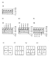
- FIGS. 1A to 1D are cross-sectional views illustrating an example of a display device.
- FIGS. 1E to 1H are top views each illustrating an example of a pixel.
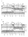
- FIGS. 2A and 2B are cross-sectional views illustrating an example of a display device.
- FIGS. 3A and 3B are cross-sectional views illustrating an example of a display device.
- FIGS. 4A and 4B are cross-sectional views illustrating an example of a display device.
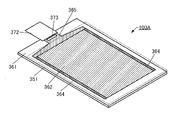
- FIG. 5 is a perspective view illustrating an example of a display device.
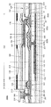
- FIG. 6 is a cross-sectional view illustrating an example of a display device.
- FIG. 7 is a cross-sectional view illustrating an example of a display device.
- FIG. 1E to 1H are top views each illustrating an example of a pixel.
- FIGS. 2A and 2B are cross-sectional views illustrating an example of a display device.
- FIGS. 3A and 3B are cross-
- FIGS. 8A and 14B are cross-sectional views illustrating an example of a method for manufacturing a display device.
- FIGS. 8A and 14B are cross-sectional views illustrating an example of a method for manufacturing a display device.
- FIGS. 15A and 15B are cross-sectional views illustrating an example of a method for manufacturing a display device.
- FIGS. 16A and 16B are cross-sectional views illustrating an example of a method for manufacturing a display device.
- FIGS. 17A and 17B are cross-sectional views illustrating an example of a method for manufacturing a display device.
- FIGS. 18A and 18B are cross-sectional views illustrating an example of a method for manufacturing a display device.
- FIGS. 19A and 19B are circuit diagrams each illustrating an example of a pixel circuit.
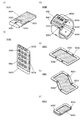
- 20A and 20B illustrate an example of an electronic device.
- FIGS. 21A and 21B illustrate an example of an electronic device.
- FIGS. 22A and 22B illustrate an example of an electronic device.
- FIGS. 23A to 23D illustrate an example of an electronic device.
- FIGS. 24A to 24F are diagrams each illustrating an example of an electronic device.
- the word “film” and the word “layer” can be interchanged with each other depending on the case or the situation.
- the term “conductive layer” can be changed to the term “conductive film”.
- the term “insulating film” can be changed to the term “insulating layer”.
- the display device of this embodiment mode includes a light receiving element and a light emitting element in a display portion. Specifically, light-emitting elements are arranged in a matrix in a display portion, and an image can be displayed on the display portion. Light-receiving elements are arranged in a matrix in the display portion, and the display portion also has a function as a light-receiving portion.
- the light receiving unit can be used for an image sensor or a touch sensor. That is, by detecting light with the light receiving unit, it is possible to capture an image and detect the proximity or contact of an object (such as a finger or a pen).
- the light-receiving element when an object reflects light emitted from the light-emitting element included in the display portion, the light-receiving element can detect the reflected light, so that imaging and touch (including near touch) detection can be performed even in a dark place. It is possible.
- the display device of this embodiment has a function of displaying an image using a light-emitting element. That is, the light-emitting element functions as a display element.
- an EL element such as an OLED (Organic Light Emitting Diode) or a QLED (Quantum-dot Light Emitting Diode) is preferably used.
- the light-emitting substance included in the EL element includes a substance that emits fluorescence (fluorescent material), a substance that emits phosphorescence (phosphorescent material), an inorganic compound (such as a quantum dot material), and a substance that exhibits heat-activated delayed fluorescence (heat-activated delayed fluorescence). (Thermally activated @ delayed @ fluorescence: TADF) material.
- an LED such as a micro LED (Light Emitting Diode) can be used.
- the display device of this embodiment has a function of detecting light using a light-receiving element.
- the display device of this embodiment can capture an image using the light receiving element.
- the display device of the present embodiment can incorporate the biometric authentication sensor. Since the display device incorporates the biometric authentication sensor, the number of components of the electronic device can be reduced as compared with the case where the biometric sensor is provided separately from the display device, and the electronic device can be reduced in size and weight. .
- data such as a facial expression of the user, eye movement, or a change in pupil diameter can be acquired using the image sensor.
- data such as a facial expression of the user, eye movement, or a change in pupil diameter
- the image sensor By analyzing the data, it is possible to obtain information on the mind and body of the user.
- By changing the output content of one or both of display and audio based on the information for example, in a device for VR (Virtual Reality), a device for AR (Augmented Reality), or a device for MR (Mixed Reality), The user can use the device safely.
- VR Virtual Reality
- AR Augmented Reality
- MR Mated Reality
- the display device of this embodiment can detect proximity or contact with an object using the light-receiving element.
- the light receiving element for example, a pn-type or pin-type photodiode can be used.
- the light receiving element functions as a photoelectric conversion element that detects light incident on the light receiving element and generates a charge. The amount of generated charges is determined based on the amount of incident light.
- organic photodiode having a layer containing an organic compound as the light receiving element.
- Organic photodiodes can be easily applied to various display devices because they can be easily reduced in thickness, weight, and area, and have a high degree of freedom in shape and design.
- FIGS. 1A to 1D are cross-sectional views of a display device of one embodiment of the present invention.
- the display device 10 illustrated in FIG. 1A includes a layer 53 including a light-receiving element, a layer 55 including a transistor, and a layer 57 including a light-emitting element between a substrate 51 and a substrate 59.
- the light receiving element is located closer to the substrate 51 than the transistor, and the light emitting element is located closer to the substrate 59 than the transistor.
- the display device 20 illustrated in FIGS. 1B to 1D includes an insulating layer 54 between a layer 53 including a light-receiving element and a layer 55 including a transistor in addition to the structure of the display device 10.
- the display device 20 illustrated in FIGS. 1B and 1C has a structure in which light enters a light-receiving element through an insulating layer 54.
- the layer 57 having a light-emitting element is provided at a position closer to the display surface of the display device 20 than the layer 53 having a light-receiving element.
- the display device 20 illustrated in FIG. 1D has a structure in which light emitted from the light-emitting element is extracted to the outside through the insulating layer 54.
- the layer 57 having a light-emitting element is provided at a position farther from the display surface of the display device 20 than the layer 53 having a light-receiving element.
- the display device 20 illustrated in FIGS. 1B and 1D has a structure in which red (R), green (G), and blue (B) light are emitted from the layer 57 having a light-emitting element. is there.
- the display device 20 illustrated in FIG. 1C is configured to emit white (W) light in addition to R, G, and B from the layer 57 including a light-emitting element.
- a display device includes a plurality of pixels arranged in a matrix.
- the pixel has one or more sub-pixels.
- the sub-pixel has one light-emitting element.
- a pixel has a configuration including three sub-pixels (three colors of R, G, and B, or three colors of yellow (Y), cyan (C), and magenta (M)), or a sub-pixel. (Four colors of R, G, B, W, or four colors of R, G, B, Y, etc.) can be applied.
- the pixel has a light receiving element.
- the light receiving element may be provided in all pixels, or may be provided in some pixels. Further, one pixel may have a plurality of light receiving elements.
- FIGS. 1E to 1H show an example of a pixel.
- the pixel illustrated in FIGS. 1E and 1F includes three sub-pixels of R, G, and B (three light-emitting elements) and a light-receiving element PD.
- FIG. 1E shows an example in which three sub-pixels and a light receiving element PD are arranged in a 2 ⁇ 2 matrix.
- FIG. 1F shows three sub-pixels and a light receiving element PD arranged in one row. This is an example in which light receiving elements PD are arranged.
- the pixel illustrated in FIG. 1G includes four sub-pixels of R, G, B, and W (four light-emitting elements) and a light-receiving element PD.
- the pixel illustrated in FIG. 1H includes three sub-pixels of R, G, and B, a light-emitting element IR that emits infrared light, and a light-receiving element PD.
- the light receiving element PD has a function of detecting infrared light.
- the light receiving element PD may have a function of detecting both visible light and infrared light.
- the wavelength of light detected by the light receiving element PD can be determined according to the use of the sensor.
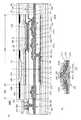
- FIG. 2A is a cross-sectional view of the display device 10A.
- the display device 10A includes a light-emitting element 170, a light-receiving element 180, a transistor 41, a transistor 42, and the like between a pair of substrates (a substrate 351 and a substrate 361).
- the display device 10A preferably further includes a lens 149. With the lens 149, the amount of light incident on the light receiving element 180 can be increased.
- the light-emitting element 170 includes an electrode 191, an EL layer 192, and an electrode 193.
- the EL layer 192 is located between the electrode 191 and the electrode 193.
- the EL layer 192 contains at least a light-emitting substance.
- the electrode 193 has a function of transmitting visible light.
- the electrode 191 preferably has a function of reflecting visible light.
- the light-emitting element 170 has a function of emitting visible light. Specifically, the light-emitting element 170 is an electroluminescent element that emits light to the substrate 351 side by applying a voltage between the electrode 191 and the electrode 193 (see Light Emission 21).
- the electrode 191 is electrically connected to a source or a drain included in the transistor 42 through an opening provided in the insulating layer 214.
- the electrode 191 has a function as a pixel electrode. An end of the electrode 191 is covered with the insulating layer 216.
- the EL layer 192 is preferably formed so as not to overlap with the light receiving region of the light receiving element 180. Thus, the absorption of the light 22 by the EL layer 192 can be suppressed, and the amount of light applied to the light receiving element 180 can be increased.
- the light-emitting element 170 is preferably covered with the protective layer 194.
- a protective layer 194 is provided in contact with the electrode 193.
- the protective layer 194 By providing the protective layer 194, entry of impurities such as water into the light-emitting element 170 can be suppressed, and the reliability of the light-emitting element 170 can be increased.
- the protective layer 194 and the substrate 351 are attached to each other with the adhesive layer 142.
- the light receiving element 180 includes an electrode 111, an organic layer 112, and an electrode 113.
- the organic layer 112 is located between the electrode 111 and the electrode 113.
- the organic layer 112 has, for example, a p-type semiconductor layer and an n-type semiconductor layer.
- the electrode 111 has a function of transmitting visible light.
- the electrode 113 preferably has a function of reflecting visible light.
- the electrode 111 is electrically connected to a source or a drain included in the transistor 41 through an opening provided in the insulating layer 212.
- the electrode 111 has a function as a pixel electrode.
- a substrate 361 is attached to the electrode 113 with an adhesive layer 141.
- the electrode 113 may be covered with a protective layer, and the protective layer and the substrate 361 may be bonded to the adhesive layer 141. This can prevent impurities from entering the light receiving element 180 and increase the reliability of the light receiving element 180.
- a light-shielding layer BM is provided on a surface of the substrate 351 on the substrate 361 side.
- the light-blocking layer BM has openings at positions overlapping the light receiving element 180 and positions overlapping the light emitting element 170.
- the light receiving element 180 detects light in which the light emission of the light emitting element 170 is reflected by the object.
- light emitted from the light emitting element 170 may be reflected in the display device and enter the light receiving element 180 without passing through the target object.
- the light-blocking layer BM can suppress the influence of such stray light.
- the light-blocking layer BM is not provided, the light 23a emitted from the light-emitting element 170 may be reflected by the substrate 351 and the reflected light 23b may enter the light-receiving element 180.
- the light shielding layer BM it is possible to suppress the reflected light 23b from being incident on the light receiving element 180. Thereby, the sensitivity of the sensor using the light receiving element 180 can be increased.
- a lens 149 is provided over the insulating layer 216.
- the lens 149 is provided at a position overlapping the light receiving element 180.
- the lens 149 may be arranged in a size according to the purpose. For example, consider the case of a display device in which the optical path length of the substrate 351 is 400 ⁇ m, the definition of the display portion is 326 ppi, and the pixel arrangement is as shown in FIG. At this time, the size of one pixel is 78 ⁇ m ⁇ , and the area occupied by one light receiving element 180 is 39 ⁇ m ⁇ . If the optical path length between the lens 149 and the light receiving element 180 is 30 ⁇ m, a 28 ⁇ m diameter hemispherical lens made of a material having a refractive index of 1.5 is preferably used as the lens 149 according to the Gaussian imaging formula.
- the light receiving element 180 obtains information in a range of 67 ⁇ m square at a point 400 ⁇ m away from the lens 149 toward the display surface side of the display device, that is, at the surface of the display device. Thus, information in a range smaller than the size of one pixel can be obtained.
- the light receiving section can have a resolution of 326 dpi and can be used for a biometric authentication sensor such as a fingerprint sensor or a touch sensor.
- the display device having the above-described configuration, when the light receiving element 180 captures information of a point at an optical path length of 50,000 ⁇ m away from the lens 149 on the display surface side of the display device, one light receiving element 180 has a range of about 8333 ⁇ m square. Get the information. In this case, by analyzing the difference in the amount of received light between the adjacent light receiving elements 180, the resolution of information can be increased. In this way, by obtaining information on a point distant from the display device, the display device can be used to acquire near-touch or image information around the display device (for example, facial expression or eye data of a user in a VR or AR device). Can be used.
- the light receiving element 180 has a function of detecting light.
- the light receiving element 180 is a photoelectric conversion element that receives the light 22 incident from the outside of the display device 10A and converts the light 22 into an electric signal.
- the light 22 can be said to be light obtained by reflecting the light emitted from the light emitting element 170 by an object. It is preferable that the light 22 is incident on the light receiving element 180 via the lens 149.
- the transistor 41 and the transistor 42 are in contact with the same layer (the insulating layer 212 in FIG. 2A).
- the transistor 41 is electrically connected to the light receiving element 180.
- the transistor 42 has a function of controlling driving of the light-emitting element 170.
- At least part of a circuit electrically connected to the light-receiving element 180 be formed using the same material and in the same step as the circuit electrically connected to the light-emitting element 170.
- the thickness of the display device can be reduced and the manufacturing process can be simplified as compared with the case where two circuits are separately formed.
- the electrode 111 is formed over the manufacturing substrate, the transistor 41 and the transistor 42 are formed, and then the lens 149 and the light-emitting element 170 are formed.
- the manufacturing substrate and the substrate 351 are attached to each other.
- the substrate 351 is attached to the manufacturing substrate so that the surface provided with the light-blocking layer BM is located on the light-emitting element 170 side.
- the electrode 111, the transistor 41, the transistor 42, the lens 149, the light-emitting element 170, and the like are transferred from the manufacturing substrate to the substrate 351.
- the electrode 111 is exposed, and the organic layer 112 and the electrode 113 are formed on the electrode 111.
- the display device 10A can be manufactured by bonding the electrode 113 and the substrate 361 to each other with the use of the adhesive layer 141.
- FIG. 2B is a cross-sectional view of the display device 10B. Note that in the following description of the display device, description of the same configuration as the display device described above may be omitted.
- the display device 10B is different from the display device 10A (FIG. 2A) in that a lens 149 is provided in contact with the substrate 351. Other configurations are the same as those of the display device 10A.
- the lens 149 of the display device 10A has a convex surface on the substrate 351 side
- the lens 149 of the display device 10B has a convex surface on the substrate 361 side.
- the lens 149 may have a convex surface on either side.
- FIG. 2B illustrates an example in which the lens 149 is formed first, the light-blocking layer BM may be formed first. In FIG. 2B, the end of the lens 149 is covered with the light shielding layer BM.
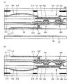
- FIG. 3A is a cross-sectional view of the display device 11A.
- the display device 11A includes a light-emitting element 170, a light-receiving element 180, the transistor 42, and the like between a pair of substrates (the substrate 351 and the circuit substrate 363).
- the display device 11A preferably further includes a lens 149. With the lens 149, the amount of light incident on the light receiving element 180 can be increased.
- the lens 149 of the display device 11A has a convex surface on the substrate 351 side.
- a sensor circuit using the light receiving element 180 such as a transistor electrically connected to the light receiving element 180, is formed.
- the light receiving element 180 is formed on a circuit board 363.
- the light receiving element 180 includes an electrode 111, an organic layer 112, and an electrode 113.
- the organic layer 112 is located between the electrode 111 and the electrode 113.
- the organic layer 112 has, for example, a p-type semiconductor layer and an n-type semiconductor layer.
- the electrode 113 has a function of transmitting visible light.
- the electrode 111 preferably has a function of reflecting visible light.
- the electrode 111 has a function as a pixel electrode. An end of the electrode 111 is covered with an insulating layer 218.
- the light receiving element 180 be covered with the protective layer 114.
- the protective layer 114 By providing the protective layer 114, impurities such as water can be prevented from entering the light receiving element 180, and the reliability of the light receiving element 180 can be improved. Then, the protective layer 114 and the insulating layer 212 are attached to each other by the adhesive layer 141.
- a transistor electrically connected to the light-emitting element 170 and a transistor electrically connected to the light-receiving element 180 have different configurations, so that a pixel circuit having the light-emitting element 170 and a sensor having the light-receiving element 180 are provided.
- a suitable configuration can be applied to each of the circuits.
- a transistor electrically connected to the light-emitting element 170 is a transistor having a metal oxide in a channel formation region
- a transistor electrically connected to the light-receiving element 180 is a transistor having silicon in a channel formation region.
- the circuit substrate 363 preferably includes a transistor in which a channel is formed in a single crystal semiconductor substrate.
- a transistor in which a channel is formed in single crystal silicon can be used as the transistor electrically connected to the light receiving element 180.
- a light-shielding layer BM is provided on the surface of the substrate 351 on the circuit substrate 363 side.
- an example of a method for manufacturing the display device 110A illustrated in FIG. First, the insulating layer 212 and the transistor 42 are formed over a manufacturing substrate, and then the lens 149 and the light-emitting element 170 are formed. Next, the manufacturing substrate and the substrate 351 are attached to each other. The substrate 351 is attached to the manufacturing substrate so that the surface provided with the light-blocking layer BM is located on the light-emitting element 170 side. Then, the insulating substrate 212, the transistor 42, the lens 149, the light-emitting element 170, and the like are transferred from the manufacturing substrate to the substrate 351 by separating the manufacturing substrate and the substrate 351 from each other. Then, the insulating layer 212 is exposed.
- the display device 110A can be manufactured by attaching the protective layer 114 and the insulating layer 212 to each other with the use of the adhesive layer 141. As described above, since the display device 110A can be manufactured by bonding the light-emitting element 170 and the circuit and the light-receiving element 180 and the circuit formed over different substrates, the display device 110A can be easily manufactured without a complicated process. be able to.
- FIG. 3B is a cross-sectional view of the display device 11B.
- the display device 11B is different from the display device 11A (FIG. 3A) in that a lens 149 is provided in contact with the substrate 351. Other configurations are the same as those of the display device 11A.
- the lens 149 of the display device 11B has a convex surface on the circuit board 363 side.
- FIG. 3B illustrates an example in which the lens 149 is formed after the light-blocking layer BM is formed first.
- an end of the light-blocking layer BM is covered with a lens 149.
- the lens 149 and the light shielding layer BM do not have to overlap.
- FIG. 4A is a cross-sectional view of the display device 12A.
- the display device 12A includes a light-emitting element 170, a light-receiving element 180, a transistor 41, a transistor 42, and the like between a pair of substrates (a substrate 351 and a substrate 361). It is preferable that the display device 12A further includes a lens array 148 on the substrate 351. With the lens array 148, the amount of light incident on the light receiving element 180 can be increased.
- the lens array 148 of the display device 12A has a convex surface on the user side.
- the light-emitting element 170 includes an electrode 191, an EL layer 192, and an electrode 193.
- the EL layer 192 is provided over a plurality of sub-pixels and a plurality of pixels.
- the electrode 191 has a function of transmitting visible light.
- the electrode 193 preferably has a function of reflecting visible light.
- the coloring layer CF is provided over the insulating layer 216.
- the coloring layer CF is provided at a position overlapping with the light-emitting element 170. It is preferable that the coloring layer CF does not overlap with the organic layer 112. Thus, the absorption of the light 22 by the colored layer CF can be suppressed, and the amount of light applied to the light receiving element 180 can be increased.
- a red sub-pixel is provided with a red coloring layer CF
- a green sub-pixel is provided with a green coloring layer CF
- a blue sub-pixel is provided with a blue coloring layer CF.
- the light emitting element 170 emit white light. Light emitted from the light-emitting element 170 is emitted to the substrate 351 side through the coloring layer CF. When the sub-pixels of each color have the coloring layers CF of different colors, full-color display can be realized.
- the light receiving element 180 is located closer to the display surface than the light emitting element 170. Therefore, even if the EL layer 192 is provided so as to overlap with the light receiving element 180, the light 22 is not blocked by the EL layer 192. Therefore, the EL layer 192 can be provided over a plurality of pixels, and the light-emitting element 170 does not need to be separately formed for each sub-pixel of each color, so that the manufacturing process can be simplified.
- the electrode 191 is electrically connected to a source or a drain included in the transistor 42 through an opening provided in the insulating layer 212.
- the electrode 191 has a function as a pixel electrode.
- the electrodes 191 of the adjacent light emitting elements 170 are insulated from each other by the insulating layer 212.
- the light-emitting element 170 is preferably covered with the protective layer 194.
- a protective layer 194 is provided in contact with the electrode 193. By providing the protective layer 194, entry of impurities into the light-emitting element 170 can be suppressed, and reliability of the light-emitting element 170 can be improved.
- a substrate 361 is attached to the protective layer 194 with an adhesive layer 141.
- the light receiving element 180 includes an electrode 111, an organic layer 112, and an electrode 113.
- the electrode 113 has a function of transmitting visible light.
- the electrode 111 preferably has a function of reflecting visible light.
- the organic layer 112 is preferably formed so as not to overlap with a light emitting region of the light emitting element 170. Thereby, the absorption of the light emission 21 by the organic layer 112 can be suppressed, and the light extraction efficiency can be increased.
- the electrode 111 is electrically connected to a source or a drain included in the transistor 41 through an opening provided in the insulating layer 214.
- the electrode 111 has a function as a pixel electrode.
- the light receiving element 180 is preferably covered with the protective layer 114.
- the protective layer 114 is provided in contact with the electrode 113.
- a substrate 351 is attached to the protective layer 114 with an adhesive layer 142.
- a lens array 148 is provided on the display surface side of the substrate 351.
- the lens of the lens array 148 is provided at a position overlapping the light receiving element 180. It is preferable that a light-blocking layer BM is provided on a surface of the substrate 351 on the substrate 361 side.
- a lens such as a microlens may be directly formed on a substrate, or a lens array such as a microlens array separately manufactured may be attached to the substrate. Is also good.
- FIG. 4B is a cross-sectional view of the display device 12B.
- the display device 12B is different from the display device 12A (FIG. 4A) in that the display device 12B does not have the lens array 148 and has the coloring layer CF over the insulating layer 212. Other configurations are the same as those of the display device 12A.
- the display device of the present embodiment may not have a lens.
- the position of the coloring layer CF is not particularly limited as long as it is between the light emitting element 170 and the substrate 351.
- the coloring layer CF is preferably formed after forming the transistor and the protective layer of the transistor. Accordingly, the temperature of the manufacturing process of the transistor can be higher than the heat-resistant temperature of the coloring layer CF, and the reliability of the transistor can be increased. Further, by providing the protective layer of the transistor, entry of impurities into the transistor at the time of forming the coloring layer CF can be suppressed.
- FIG. 4A illustrates an example in which the coloring layer CF is provided in contact with the insulating layer 216.
- FIG. 4B illustrates an example in which the coloring layer CF is provided over the insulating layer 212 and the transistor 42.
- FIG. 5 shows a perspective view of the display device 100A
- FIG. 6 shows a cross-sectional view of the display device 100A.
- the display device 100A has a structure in which a substrate 351 and a substrate 361 are attached to each other.
- the substrate 351 is clearly indicated by a broken line.
- the display device 100A includes a display portion 362, a circuit 364, a wiring 365, and the like.
- FIG. 5 illustrates an example in which an IC (integrated circuit) 373 and an FPC 372 are mounted on the display device 100A. Therefore, the structure illustrated in FIG. 5 can be regarded as a display module including the display device 100A, the IC, and the FPC.
- a scan line driver circuit can be used.
- the wiring 365 has a function of supplying a signal and power to the display portion 362 and the circuit 364.
- the signal and the power are input to the wiring 365 from the outside through the FPC 372 or from the IC 373.
- FIG. 5 illustrates an example in which the IC 373 is provided on the substrate 361 by a COG (Chip On Glass) method, a COF (Chip On Film) method, or the like.
- the IC 373 for example, an IC including a scan line driver circuit, a signal line driver circuit, or the like can be used.
- the display device 100A and the display module may have a structure in which an IC is not provided. Further, the IC may be mounted on the FPC by a COF method or the like.
- FIG. 6 illustrates a part of the region including the FPC 372, the part of the region including the circuit 364, the part of the region including the display portion 362, and the one including the end portion of the display device 100A illustrated in FIG. 5 shows an example of a cross section when each part is cut.
- the display device 100A illustrated in FIG. 6 includes a transistor 201, a transistor 205, a transistor 206, a light-emitting element 170, a light-receiving element 180, a lens 149, and the like between the substrate 351 and the substrate 361.
- the substrate 361 and the insulating layer 212 are bonded via the bonding layer 141.
- the substrate 351 and the insulating layer 214 are bonded via the bonding layer 142.
- a solid sealing structure, a hollow sealing structure, or the like can be applied, respectively.
- the adhesive layer 141 is provided so as to overlap the light receiving element 180, and a solid sealing structure is applied.
- a space 143 surrounded by the substrate 351, the adhesive layer 142, and the insulating layer 214 is filled with an inert gas (such as nitrogen or argon), and a hollow sealing structure is applied.
- the adhesive layer 142 may be provided so as to overlap with the light-emitting element 170.
- the space 143 surrounded by the substrate 351, the adhesive layer 142, and the insulating layer 214 may be filled with a resin different from that of the adhesive layer 142.
- the light-emitting element 170 has a stacked structure in which an electrode 191, an EL layer 192, and an electrode 193 are stacked in this order from the insulating layer 214 side.
- the electrode 191 is connected to a conductive layer 222b included in the transistor 206 through an opening provided in the insulating layer 214.
- the transistor 206 has a function of controlling driving of the light-emitting element 170.
- An insulating layer 216 covers the end of the electrode 191.
- the electrode 191 includes a material that reflects visible light
- the electrode 193 includes a material that transmits visible light. Light emitted from the light-emitting element 170 is emitted to the substrate 351 side.
- the light receiving element 180 has a stacked structure in which the electrode 111, the organic layer 112, and the electrode 113 are stacked in this order from the insulating layer 212 side.
- the electrode 111 is connected to the conductive layer 221b through an opening provided in the insulating layer 212.
- the conductive layer 221b is connected to the conductive layer 222b included in the transistor 205. That is, in the connection portion 207, the electrode 111 is electrically connected to the conductive layer 222b included in the transistor 205 through the conductive layer 221b.
- the electrode 111 includes a material that transmits visible light
- the electrode 113 includes a material that reflects visible light.
- the electrode 111 which is a pixel electrode of the light receiving element 180 is located opposite to the electrode 191 which is a pixel electrode of the light emitting element 170 with the insulating layer 211 included in the transistors 205 and 206 interposed therebetween.
- a light-shielding layer BM is provided on a surface of the substrate 351 on the substrate 361 side.
- the light-blocking layer BM has an opening at a position overlapping the light receiving element 180 and a position overlapping the light emitting element 170.
- the light-blocking layer BM a material that blocks light emission from the light-emitting element can be used.
- a black matrix can be formed using a metal material, a resin material containing a pigment or a dye, or the like.
- the light-blocking layer BM is preferably provided in a region other than the display portion 362 such as the circuit 364 because unintended light leakage due to guided light or the like can be suppressed.
- the lens 149 is provided in contact with the insulating layer 216.
- the lens 149 has a convex surface on the substrate 351 side.
- the light receiving region of the light receiving element 180 preferably overlaps the lens 149 and does not overlap the EL layer 192. Thereby, the sensitivity and accuracy of the sensor using the light receiving element 180 can be improved.
- the transistors 201, 205, and 206 are all formed over the insulating layer 212. These transistors can be manufactured by the same process.
- the insulating layer 211, the insulating layer 213, the insulating layer 215, and the insulating layer 214 are provided over the insulating layer 212 in this order.
- Part of the insulating layer 211 functions as a gate insulating layer of each transistor.
- Part of the insulating layer 213 functions as a gate insulating layer of each transistor.
- the insulating layer 215 is provided to cover the transistor.
- the insulating layer 214 is provided so as to cover the transistor and has a function as a planarization layer. Note that the number of insulating layers covering the transistor is not limited, and may be a single layer or two or more layers.
- At least one layer of the insulating layer covering the transistor be formed using a material to which impurities such as water and hydrogen are unlikely to diffuse.
- the insulating layer can function as a barrier layer.
- the organic insulating film often has lower barrier properties than the inorganic insulating film. Therefore, the organic insulating film preferably has an opening near the end of the display device. Accordingly, entry of impurities from the end of the display device through the organic insulating film can be suppressed.
- the organic insulating film may be formed such that the end of the organic insulating film is located inside the end of the display device so that the organic insulating film is not exposed at the end of the display device.
- An organic insulating film is preferably used for the insulating layer 214 functioning as a planarizing layer.
- an opening is formed in the insulating layer 214. Accordingly, even when an organic insulating film is used for the insulating layer 214, entry of impurities from the outside into the display portion 362 through the insulating layer 214 can be suppressed. Therefore, the reliability of the display device 100A can be improved.
- the transistors 201, 205, and 206 each include a conductive layer 221a functioning as a gate, an insulating layer 211 functioning as a gate insulating layer, conductive layers 222a and 222b functioning as a source and a drain, a semiconductor layer 231, and a gate insulating layer. And a conductive layer 223 functioning as a gate.
- the same hatching pattern is given to a plurality of layers obtained by processing the same conductive film.
- the insulating layer 211 is located between the conductive layer 221a and the semiconductor layer 231.
- the insulating layer 213 is located between the conductive layer 223 and the semiconductor layer 231.
- the structure of the transistor included in the display device of this embodiment is not particularly limited.
- a planar transistor, a staggered transistor, an inverted staggered transistor, or the like can be used.
- either a top-gate transistor structure or a bottom-gate transistor structure may be employed.
- gates may be provided above and below a semiconductor layer in which a channel is formed.
- a structure in which a semiconductor layer in which a channel is formed is sandwiched between two gates is applied to the transistor 201, the transistor 205, and the transistor 206.
- the transistor may be driven by connecting two gates and supplying the same signal to them.
- a threshold voltage of a transistor may be controlled by applying a potential for controlling a threshold voltage to one of two gates and a potential for driving to the other of the two gates.
- crystallinity of a semiconductor material used for the transistor there is no particular limitation on the crystallinity of a semiconductor material used for the transistor, either an amorphous semiconductor or a semiconductor having crystallinity (a microcrystalline semiconductor, a polycrystalline semiconductor, a single crystal semiconductor, or a semiconductor partially having a crystalline region). May be used. It is preferable to use a semiconductor having crystallinity because deterioration of transistor characteristics can be suppressed.
- the semiconductor layer of the transistor preferably includes a metal oxide (also referred to as an oxide semiconductor).
- the semiconductor layer of the transistor may include silicon. Examples of silicon include amorphous silicon and crystalline silicon (such as low-temperature polysilicon and single-crystal silicon).
- the semiconductor layer includes, for example, indium and M (M is gallium, aluminum, silicon, boron, yttrium, tin, copper, vanadium, beryllium, titanium, iron, nickel, germanium, zirconium, molybdenum, lanthanum, cerium, neodymium, One or more selected from hafnium, tantalum, tungsten, and magnesium) and zinc.
- M is preferably one or more selected from aluminum, gallium, yttrium, and tin.
- an oxide containing indium (In), gallium (Ga), and zinc (Zn) (also referred to as IGZO) is preferably used as the semiconductor layer.
- the sputtering target used for forming the In-M-Zn oxide preferably has an atomic ratio of In equal to or higher than the atomic ratio of M.
- the atomic ratio of the semiconductor layer to be formed includes a variation of ⁇ 40% of the atomic ratio of the metal element included in the sputtering target.
- the transistor included in the circuit 364 and the transistor included in the display portion 362 may have the same structure or different structures.
- the structure of the plurality of transistors included in the circuit 364 may be the same, or may be two or more.
- the structure of the plurality of transistors included in the display portion 362 may be the same, or may be two or more.
- connection portion 204 is provided in a region where the substrate 361 and the substrate 351 do not overlap.
- the wiring 365 is electrically connected to the FPC 372 through the conductive layer 366 and the connection layer 242.
- a conductive layer 366 obtained by processing the same conductive film as the electrode 191 is exposed on the upper surface of the connection portion 204.
- the connection portion 204 and the FPC 372 can be electrically connected via the connection layer 242.
- optical members can be arranged outside the substrate 351.
- the optical member include a polarizing plate, a retardation plate, a light diffusion layer (such as a diffusion film), an antireflection layer, and a light-collecting film.
- a polarizing plate for suppressing adhesion of dust
- a water-repellent film for preventing adhesion of dirt
- a hard coat film for suppressing generation of scratches due to use
- a shock absorbing layer and the like are arranged. You may.
- Glass, quartz, ceramic, sapphire, organic resin, or the like can be used for the substrate 351 and the substrate 361, respectively.
- the flexibility of the display device can be increased.
- various curable adhesives such as a photocurable adhesive such as an ultraviolet curable adhesive, a reaction curable adhesive, a thermosetting adhesive, and an anaerobic adhesive
- the adhesive include an epoxy resin, an acrylic resin, a silicone resin, a phenol resin, a polyimide resin, an imide resin, a PVC (polyvinyl chloride) resin, a PVB (polyvinyl butyral) resin, and an EVA (ethylene vinyl acetate) resin.
- a material having low moisture permeability such as an epoxy resin is preferable.
- a two-pack type resin may be used.
- an adhesive sheet or the like may be used.
- connection layer 242 an anisotropic conductive film (ACF: Anisotropic Conductive Film), an anisotropic conductive paste (ACP: Anisotropic Conductive Paste), or the like can be used.
- ACF Anisotropic Conductive Film
- ACP Anisotropic Conductive Paste
- the light-emitting element 170 includes a top emission type, a bottom emission type, a dual emission type, and the like.
- a conductive film that transmits visible light is used for the electrode from which light is extracted. It is preferable to use a conductive film that reflects visible light for the electrode on the side from which light is not extracted.
- the EL layer 192 has at least a light-emitting layer.
- the EL layer 192 is a layer other than the light-emitting layer as a substance having a high hole-injection property, a substance having a high hole-transport property, a hole-blocking material, a substance having a high electron-transport property, a substance having a high electron-injection property, (A substance having a high electron-transport property and a high hole-transport property) may be further provided.
- Either a low molecular compound or a high molecular compound can be used for the EL layer 192, and the EL layer 192 may contain an inorganic compound.
- Each of the layers included in the EL layer 192 can be formed by a method such as an evaporation method (including a vacuum evaporation method), a transfer method, a printing method, an inkjet method, and a coating method.
- the EL layer 192 may include an inorganic compound such as a quantum dot.
- an inorganic compound such as a quantum dot.
- the quantum dot can function as a light emitting material.
- the light receiving element 180 has an active layer between a pair of electrodes.
- the active layer includes a semiconductor.
- the semiconductor include an inorganic semiconductor such as silicon and an organic semiconductor including an organic compound.
- an organic semiconductor is used as a semiconductor included in the active layer.
- the EL layer 192 of the light-emitting element 170 and the organic layer 112 of the light-receiving element 180 can be formed by the same method (for example, a vacuum evaporation method), and a manufacturing apparatus can be shared, which is preferable. .
- an electron-accepting organic semiconductor material such as fullerene (for example, C 60 or C 70 ) or a derivative thereof can be given.
- Examples of the material of the p-type semiconductor included in the organic layer 112 include an electron-donating organic semiconductor material such as copper (II) phthalocyanine (CuPc) or tetraphenyldibenzoperiflanthene (DBP). Is mentioned.
- the organic layer 112 may have a stacked structure (a pn stacked structure) of an electron-accepting semiconductor material and an electron-donating semiconductor material, or an electron-accepting semiconductor material and an electron-donating semiconductor material therebetween.
- a stacked structure pin stacked structure
- a hole block layer or an electron block layer is formed around (upper or lower side) of the pn stacked structure or the pin stacked structure. May be provided.
- the lens 149 preferably has a refractive index of 1.3 or more and 2.5 or less.
- the lens 149 can be formed using an inorganic material or an organic material.
- a material containing a resin can be used for the lens 149.
- a material containing an oxide or a sulfide can be used for the lens 149.
- a resin containing chlorine, bromine, or iodine, a resin containing a heavy metal atom, a resin containing an aromatic ring, a resin containing sulfur, or the like can be used for the lens 149.
- a material including a resin and nanoparticles of a material having a higher refractive index than the resin can be used for the lens 149. Titanium oxide or zirconium oxide can be used for the nanoparticles.
- zinc sulfide or the like can be used for the lens 149.
- materials that can be used for conductive layers such as various wirings and electrodes included in a display device include aluminum, titanium, chromium, nickel, copper, yttrium, zirconium, molybdenum, silver, A metal such as tantalum or tungsten, or an alloy mainly containing such a metal is given. A film containing any of these materials can be used as a single layer or as a stacked structure.
- a conductive oxide such as indium oxide, indium tin oxide, indium zinc oxide, zinc oxide, or zinc oxide containing gallium, or graphene
- a metal material such as gold, silver, platinum, magnesium, nickel, tungsten, chromium, molybdenum, iron, cobalt, copper, palladium, or titanium, or an alloy material containing the metal material
- a nitride of the metal material for example, titanium nitride
- a metal material or an alloy material (or a nitride thereof) it is preferable that the thickness be small enough to have a light-transmitting property.
- a stacked film of the above materials can be used as the conductive layer.
- a stacked film of an alloy of silver and magnesium and indium tin oxide is preferably used because conductivity can be increased.
- These can be used for a conductive layer such as various wirings and electrodes included in a display device, and a conductive layer included in a display element (a conductive layer functioning as a pixel electrode or a common electrode).
- Examples of an insulating material that can be used for each insulating layer include a resin such as an acrylic resin and an epoxy resin, and an inorganic insulating material such as silicon oxide, silicon oxynitride, silicon nitride oxide, silicon nitride, and aluminum oxide.
- a resin such as an acrylic resin and an epoxy resin
- an inorganic insulating material such as silicon oxide, silicon oxynitride, silicon nitride oxide, silicon nitride, and aluminum oxide.
- FIG. 7 shows a cross-sectional view of the display device 100B.
- the display device 100B mainly includes the protective layer 114 and the protective layer 194, the transistor 205 does not include the conductive layer 223, and the lens 149 is provided in contact with the substrate 351. And different.
- the protective layer 114 that covers the light receiving element 180, entry of impurities into the light receiving element 180 can be suppressed, and the reliability of the light receiving element 180 can be improved.
- the protective layer 194 that covers the light-emitting element 170 By providing the protective layer 194 that covers the light-emitting element 170, entry of impurities into the light-emitting element 170 can be suppressed, and reliability of the light-emitting element 170 can be improved.
- the insulating layer 215 and the protective layer 194 are preferably in contact with each other through an opening in the insulating layer 214.
- the inorganic insulating film included in the insulating layer 215 and the inorganic insulating film included in the protective layer 194 be in contact with each other. Accordingly, it is possible to prevent impurities from entering the display portion 362 from outside via the organic insulating film. Therefore, the reliability of the display device 100B can be improved.
- a lens 149 is provided on a surface of the substrate 351 on the substrate 361 side.
- the transistor 201 and the transistor 206 have the conductive layer 223, and the transistor 205 does not have the conductive layer 223.
- a transistor having two or more types of structures may be used in the display device.
- FIG. 8A is a cross-sectional view of the display device 100C.
- the display device 100C mainly differs from the display device 100B in the structure of the transistor.
- a transistor included in the display device 100C will be described.
- the display device 100C includes the transistor 208, the transistor 209, and the transistor 210 over the insulating layer 212.
- the transistor 208, the transistor 209, and the transistor 210 each include a conductive layer 221a functioning as a gate, an insulating layer 211 functioning as a gate insulating layer, a semiconductor layer including a channel formation region 231i and a pair of low-resistance regions 231n, and a pair of low-resistance regions. 231n, a conductive layer 222a connected to one of the conductive layers 231n, an insulating layer 225 functioning as a gate insulating layer, a conductive layer 223 functioning as a gate, and an insulating layer 215 covering the conductive layer 223.
- the transistors 208 and 210 each further include a conductive layer 222b connected to the other of the pair of low-resistance regions 231n.
- the insulating layer 211 is located between the conductive layer 221a and the channel formation region 231i.
- the insulating layer 225 is located between the conductive layer 223 and the channel formation region 231i.
- the conductive layers 222a and 222b are connected to the low-resistance regions 231n through openings provided in the insulating layers 225 and 215, respectively.
- One of the conductive layers 222a and 222b functions as a source, and the other functions as a drain.
- the electrode 191 of the light-emitting element 170 is electrically connected to one of the pair of low-resistance regions 231n of the transistor 208 through the conductive layer 222b.
- the electrode 111 of the light-receiving element 180 is electrically connected to the other of the pair of low-resistance regions 231n of the transistor 209 through the conductive layer 221b.
- FIG. 8A illustrates an example in which the insulating layer 225 covers the top surface and side surfaces of the semiconductor layer.
- the insulating layer 225 overlaps with the channel formation region 231i of the semiconductor layer 231 and does not overlap with the low-resistance region 231n.
- the structure illustrated in FIG. 8B can be manufactured by processing the insulating layer 225 using the conductive layer 223 as a mask.
- an insulating layer 215 is provided to cover the insulating layer 225 and the conductive layer 223, and the conductive layers 222a and 222b are connected to the low-resistance regions 231n through openings in the insulating layer 215. I have.
- an insulating layer 217 which covers the transistor may be provided.
- FIG. 9 is a cross-sectional view of the display unit 362 of the display device 110A.
- the display device 110A illustrated in FIG. 9 includes a transistor 202, a transistor 206, a light-emitting element 170, a light-receiving element 180, a lens 149, and the like between the semiconductor substrate 251 and the substrate 351.
- the light emitting element 170 is sealed with the substrate 351 and the adhesive layer 142.
- the structures of the transistor 206 and the light-emitting element 170 are similar to those of the display device 100A illustrated in FIG.
- the transistor 206 and the light-emitting element 170 are provided over the insulating layer 212.
- the light receiving element 180 formed over the circuit board 363 is attached to the insulating layer 212 with an adhesive layer 141.
- a stacked structure from the semiconductor substrate 251 to the insulating layer 266 corresponds to the circuit substrate 363 illustrated in FIG.
- a circuit substrate 363 illustrated in FIG. 9 includes the transistor 202 in which a channel is formed in the semiconductor substrate 251.
- the semiconductor substrate 251 a single crystal silicon substrate is preferable.
- the transistor 202 includes a conductive layer 259, an insulating layer 257, an insulating layer 258, and a pair of low-resistance regions 255.
- the conductive layer 259 functions as a gate.
- the insulating layer 257 is located between the conductive layer 259 and the semiconductor substrate 251, and functions as a gate insulating layer.
- the insulating layer 258 is provided to cover a side surface of the conductive layer 259 and functions as a sidewall.
- the pair of low-resistance regions 255 is a region in the semiconductor substrate 251 to which an impurity is doped, and one functions as a source of the transistor 202 and the other functions as a drain of the transistor 202.
- an element isolation layer 253 is provided between two adjacent transistors so as to be embedded in the semiconductor substrate 251.
- An insulating layer 262 is provided to cover the transistor 202, and the capacitor 240 is provided over the insulating layer 262.
- the capacitor 240 has a structure in which a conductive layer 263, an insulating layer 264, and a conductive layer 265 are sequentially stacked from the insulating layer 262 side.
- the conductive layer 263 functions as one electrode
- the conductive layer 265 functions as the other electrode
- the insulating layer 264 functions as a dielectric.
- the conductive layer 263 is electrically connected to the low-resistance region 255 of the transistor 202 through a plug 261 provided in the insulating layer 262.
- the insulating layer 264 is provided to cover the conductive layer 263.
- the conductive layer 265 overlaps with the conductive layer 263 with the insulating layer 264 provided therebetween.
- An insulating layer 266 is provided to cover the capacitor 240, and the light-receiving element 180 is provided over the insulating layer 266.
- the light receiving element 180 has a stacked structure in which the electrode 111, the organic layer 112, and the electrode 113 are stacked in this order from the insulating layer 266 side.
- the electrode 111 is electrically connected to the conductive layer 263 through a plug 267 provided in the insulating layer 264 and the insulating layer 266.
- the conductive layer 263 is electrically connected to the low-resistance region 255 included in the transistor 202 through the plug 261. That is, the electrode 111 is electrically connected to the source or the drain of the transistor 202.
- An end of the electrode 111 is covered with an insulating layer 219.
- the electrode 111 includes a material that reflects visible light
- the electrode 113 includes a material that transmits visible light.
- the lens 149 is provided in contact with the insulating layer 216.
- the lens 149 has a convex surface on the substrate 351 side.
- the light receiving region of the light receiving element 180 preferably overlaps the lens 149 and does not overlap the EL layer 192. Thereby, the sensitivity and accuracy of the sensor using the light receiving element 180 can be improved.
- a light-shielding layer BM is provided on the surface of the substrate 351 on the circuit substrate 363 side.
- FIG. 10 shows a cross-sectional view of the display device 110B.
- the display device 110B illustrated in FIG. 10 includes a transistor 203, a transistor 206, a light-emitting element 170, a light-receiving element 180, a lens 149, and the like between the substrate 252 and the substrate 351.
- the light-emitting element 170 is covered with the protective layer 194 and further sealed with the substrate 351 and the adhesive layer 142.
- the structures of the transistor 206 and the light-emitting element 170 are similar to those of the display device 100B illustrated in FIG.
- the transistor 206 and the light-emitting element 170 are provided over the insulating layer 212.
- the light receiving element 180 and the protective layer 114 formed over the circuit board 363 are attached to the insulating layer 212 with an adhesive layer 141.
- a stacked structure from the substrate 252 to the insulating layer 288 corresponds to the circuit substrate 363 illustrated in FIG.
- a circuit board 363 illustrated in FIG. 10 includes the transistor 203 over a substrate 252.
- an insulating substrate such as a glass substrate, a quartz substrate, a sapphire substrate, or a ceramic substrate, a single crystal semiconductor substrate formed using silicon, silicon carbide, or the like, a polycrystalline semiconductor substrate, or a compound semiconductor substrate such as silicon germanium And a semiconductor substrate such as an SOI substrate.
- An insulating layer 271 is provided over the substrate 252.
- the insulating layer 271 functions as a barrier layer for preventing impurities such as water and hydrogen from the substrate 252 from diffusing into the transistor 203 and preventing oxygen from being released from the semiconductor layer 276 to the insulating layer 271 side.
- a film such as an aluminum oxide film, a hafnium oxide film, or a silicon nitride film, to which hydrogen and oxygen are less likely to diffuse than a silicon oxide film can be used.
- the transistor 203 includes a conductive layer 272, an insulating layer 273, an insulating layer 274, an insulating layer 275, a semiconductor layer 276, a pair of conductive layers 277, an insulating layer 278, a conductive layer 279, and the like.
- the semiconductor layer 276 preferably contains a metal oxide.
- a conductive layer 272 and an insulating layer 273 are provided over the insulating layer 271, and an insulating layer 274 and an insulating layer 275 are provided so as to cover the conductive layer 272 and the insulating layer 273.
- the semiconductor layer 276 is provided over the insulating layer 275.
- the conductive layer 272 functions as a gate, and the insulating layers 274 and 275 function as gate insulating layers.
- the conductive layer 272 overlaps with the semiconductor layer 276 with the insulating layer 274 and the insulating layer 275 interposed therebetween.
- the insulating layer 274 preferably functions as a barrier layer, like the insulating layer 271.
- an oxide insulating film such as a silicon oxide film is preferably used.
- the pair of conductive layers 277 is provided over the semiconductor layer 276 so as to be apart from each other.
- the pair of conductive layers 277 functions as a source and a drain.
- An insulating layer 281 is provided so as to cover the semiconductor layer 276 and the pair of conductive layers 277, and the insulating layer 282 is provided over the insulating layer 281.
- An opening reaching the semiconductor layer 276 is provided in the insulating layers 281 and 282, and the insulating layer 278 and the conductive layer 279 are embedded in the openings.
- an insulating layer 283 and an insulating layer 284 are provided so as to cover upper surfaces of the insulating layer 282, the insulating layer 278, and the conductive layer 279.
- the conductive layer 279 functions as a gate, and the insulating layer 278 functions as a gate insulating layer.
- the conductive layer 279 overlaps with the semiconductor layer 276 with the insulating layer 278 interposed therebetween.
- the insulating layers 281 and 283 preferably function as barrier layers, similarly to the insulating layer 271.
- a plug electrically connected to one of the pair of conductive layers 277 and the conductive layer 285 is embedded in an opening provided in the insulating layer 281, the insulating layer 282, the insulating layer 283, and the insulating layer 284.
- the plug preferably has a conductive layer 261a in contact with the side surface of the opening and one upper surface of the pair of conductive layers 277, and a conductive layer 261b embedded inside the conductive layer 261a. At this time, it is preferable that a conductive material through which hydrogen and oxygen hardly diffuse is used for the conductive layer 261a.
- the capacitor 245 is provided over the insulating layer 284.
- the capacitor 245 has a structure in which a conductive layer 285, an insulating layer 286, and a conductive layer 287 are stacked in this order from the insulating layer 284 side.
- the conductive layer 285 functions as one electrode
- the conductive layer 287 functions as the other electrode
- the insulating layer 286 functions as a dielectric.
- the insulating layer 286 is provided to cover the conductive layer 285, and the conductive layer 287 overlaps with the conductive layer 285 with the insulating layer 286 provided therebetween.
- An insulating layer 288 is provided to cover the capacitor 245, and the light-receiving element 180 is provided over the insulating layer 288.
- the light receiving element 180 has a stacked structure in which the electrode 111, the organic layer 112, and the electrode 113 are stacked in this order from the insulating layer 288 side.
- the light receiving element 180 is covered with the protective layer 114.
- the electrode 111 is electrically connected to the conductive layer 285 through a plug 289 provided in the insulating layers 286 and 288.
- the conductive layer 285 is electrically connected to one of the pair of conductive layers 277 through a plug. That is, the electrode 111 is electrically connected to the source or the drain of the transistor 203.
- the electrode 111 includes a material that reflects visible light
- the electrode 113 includes a material that transmits visible light.
- the lens 149 is provided on the surface of the substrate 351 on the substrate 252 side.
- the lens 149 has a convex surface on the substrate 252 side.
- the light receiving region of the light receiving element 180 preferably overlaps the lens 149 and does not overlap the EL layer 192. Thereby, the sensitivity and accuracy of the sensor using the light receiving element 180 can be improved.
- a light-shielding layer BM is provided on the surface of the substrate 351 on the circuit substrate 363 side.
- FIG. 11 is a cross-sectional view of the display device 120A.
- the display device 120A illustrated in FIG. 11 includes a transistor 201, a transistor 205, a transistor 206, a light-emitting element 170, a light-receiving element 180, a lens array 148, and the like between the substrate 351 and the substrate 361.
- the substrate 361 and the protective layer 194 are bonded via an adhesive layer 141.
- the substrate 351 and the protective layer 114 are bonded via an adhesive layer 142.
- a lens array 148 is provided on the display surface side of the substrate 351. It is preferable that a light-blocking layer BM is provided on a surface of the substrate 351 on the substrate 361 side.
- the light-emitting element 170 has a stacked structure in which an electrode 191, an EL layer 192, and an electrode 193 are stacked in this order from the insulating layer 212 side.
- the electrode 191 is connected to the conductive layer 221b through an opening provided in the insulating layer 212.
- the conductive layer 221b is connected to the conductive layer 222b included in the transistor 206. That is, in the connection portion 207, the electrode 191 is electrically connected to the conductive layer 222b included in the transistor 206 through the conductive layer 221b.
- the transistor 206 has a function of controlling driving of the light-emitting element 170.
- the electrode 191 includes a material that transmits visible light
- the electrode 193 includes a material that reflects visible light.
- Light emitted from the light-emitting element 170 is emitted toward the substrate 351 through the insulating layer 212, the insulating layer 214, the insulating layer 216, the coloring layer CF, the electrode 113, the protective layer 114, the adhesive layer 142, and the like. It is preferable to use a material having high transmittance to visible light for these layers.
- the light receiving element 180 has a stacked structure in which the electrode 111, the organic layer 112, and the electrode 113 are stacked in this order from the insulating layer 214 side.
- the electrode 111 is connected to a conductive layer 222b included in the transistor 205 through an opening provided in the insulating layer 214.
- An insulating layer 216 covers the end of the electrode 111.
- the electrode 111 includes a material that reflects visible light
- the electrode 113 includes a material that transmits visible light. Light enters the light receiving element 180 via the lens array 148, the substrate 351, the adhesive layer 142, and the like.
- the coloring layer CF is provided over the insulating layer 216.
- the coloring layer CF preferably overlaps with the light-emitting element 170 and does not overlap with the organic layer 112. Thereby, the sensitivity and accuracy of the sensor using the light receiving element 180 can be improved.
- the coloring layer is a colored layer that transmits light in a specific wavelength range.
- a color filter that transmits light in a red, green, blue, or yellow wavelength range can be used.
- Examples of a material that can be used for the coloring layer include a metal material, a resin material, and a resin material containing a pigment or a dye.
- FIG. 12 shows a cross-sectional view of the display device 120B.
- the display device 120B is different from the display device 120A (FIG. 11) in that the display device 120B does not have the lens array 148 and has a coloring layer CF in contact with the insulating layer 215. Other configurations are the same as those of the display device 120A.
- the coloring layer CF be formed after the insulating layer 215 functioning as a barrier layer of the transistor is formed, because impurities can be prevented from entering the transistor in the manufacturing process of the coloring layer CF, whereby reliability of the transistor can be improved.
- Metal oxide Hereinafter, a metal oxide applicable to the semiconductor layer will be described.
- a metal oxide containing nitrogen may be collectively referred to as a metal oxide (metal oxide). Further, a metal oxide containing nitrogen may be referred to as metal oxynitride. For example, a metal oxide containing nitrogen such as zinc oxynitride (ZnON) may be used for the semiconductor layer.
- metal oxide metal oxide
- ZnON zinc oxynitride
- CAAC c-axis @ aligned crystal
- CAC Cloud-Aligned @ Composite
- CAC-OS Cloud-Aligned Composite Oxide Semiconductor
- the CAC-OS or CAC-metal oxide includes a conductive function in part of a material, an insulating function in part of a material, and a semiconductor function as a whole of the material.
- the conductive function is a function of flowing electrons (or holes) serving as carriers
- the insulating function is a function of flowing electrons (carriers). It is a function that does not flow.
- the CAC-OS or CAC-metal oxide includes a conductive region and an insulating region.
- the conductive region has the above-described conductive function
- the insulating region has the above-described insulating function.
- a conductive region and an insulating region are separated at a nanoparticle level in a material. Further, the conductive region and the insulating region may be unevenly distributed in the material. In some cases, the conductive region is observed with its periphery blurred and connected in a cloud shape.
- the conductive region and the insulating region each have a size of 0.5 nm to 10 nm, preferably 0.5 nm to 3 nm, and are dispersed in a material. There is.
- CAC-OS or CAC-metal oxide includes components having different band gaps.
- a CAC-OS or a CAC-metal oxide includes a component having a wide gap due to an insulating region and a component having a narrow gap due to a conductive region.
- the carrier when the carrier flows, the carrier mainly flows in the component having the narrow gap.
- the component having the narrow gap acts complementarily to the component having the wide gap, and the carrier flows to the component having the wide gap in conjunction with the component having the narrow gap. Therefore, in the case where the CAC-OS or CAC-metal oxide is used for a channel formation region of a transistor, high current driving capability, that is, a high on-state current and high field-effect mobility can be obtained when the transistor is on.
- CAC-OS or the CAC-metal oxide may be referred to as a matrix composite (metal @ composite) or a metal matrix composite (metal @ matrix @ composite).
- An oxide semiconductor is classified into a single crystal oxide semiconductor and a non-single-crystal oxide semiconductor.
- a non-single-crystal oxide semiconductor for example, a CAAC-OS (c-axis aligned crystalline oxide semiconductor), a polycrystalline oxide semiconductor, an nc-OS (nanocrystalline oxide semiconductor), and a pseudo-amorphous oxide semiconductor (a-like) OS: amorphous-like oxide semiconductor, an amorphous oxide semiconductor, or the like.
- the CAAC-OS has a c-axis orientation and a crystal structure in which a plurality of nanocrystals are connected in an ab plane direction and has a strain.
- the strain refers to a region where the orientation of the lattice arrangement changes between a region where the lattice arrangement is uniform and a region where another lattice arrangement is uniform in a region where a plurality of nanocrystals are connected.
- the nanocrystal is basically a hexagon, but is not limited to a regular hexagon and may be a non-regular hexagon.
- distortion may have a lattice arrangement such as a pentagon and a heptagon.
- a clear crystal grain boundary also referred to as a grain boundary
- the formation of crystal grain boundaries is suppressed by the distortion of the lattice arrangement. This is because the CAAC-OS can tolerate distortion because the arrangement of oxygen atoms is not dense in the ab plane direction, or the bonding distance between atoms changes by substitution with a metal element. That's why.
- the CAAC-OS is a layered crystal in which a layer containing indium and oxygen (hereinafter, an In layer) and a layer containing elements M, zinc, and oxygen (hereinafter, an (M, Zn) layer) are stacked. It tends to have a structure (also called a layered structure).
- indium and the element M can be replaced with each other, and when the element M in the (M, Zn) layer is replaced with indium, it can also be referred to as an (In, M, Zn) layer.
- indium in the In layer is replaced with the element M, it can be referred to as an (In, M) layer.
- CAAC-OS is a metal oxide with high crystallinity.
- CAAC-OS it is difficult to confirm a clear crystal grain boundary; thus, it can be said that electron mobility due to the crystal grain boundary is not easily reduced.
- CAAC-OS impurities and defects oxygen deficiency (V O:. Oxygen vacancy also referred) etc.) with less metal It can also be called an oxide. Therefore, a metal oxide having a CAAC-OS has stable physical properties. Therefore, the metal oxide including the CAAC-OS is resistant to heat and has high reliability.
- the nc-OS has a periodic atomic arrangement in a minute region (for example, a region with a thickness of 1 nm to 10 nm, particularly, a region with a size of 1 nm to 3 nm).
- a minute region for example, a region with a thickness of 1 nm to 10 nm, particularly, a region with a size of 1 nm to 3 nm.
- the nc-OS may not be distinguished from an a-like @ OS or an amorphous oxide semiconductor.
- indium-gallium-zinc oxide which is a kind of metal oxide including indium, gallium, and zinc
- IGZO indium-gallium-zinc oxide
- a smaller crystal for example, the above-described nanocrystal
- a large crystal here, a crystal of several mm or a crystal of several cm.
- it may be structurally stable.
- a-like @ OS is a metal oxide having a structure between an nc-OS and an amorphous oxide semiconductor.
- a-like @ OS has voids or low density regions. That is, a-like @ OS has lower crystallinity than the nc-OS and the CAAC-OS.
- Oxide semiconductors have various structures and each have different characteristics.
- the oxide semiconductor of one embodiment of the present invention may include two or more of an amorphous oxide semiconductor, a polycrystalline oxide semiconductor, an a-like @ OS, an nc-OS, and a CAAC-OS.
- the metal oxide film functioning as a semiconductor layer can be formed using one or both of an inert gas and an oxygen gas.
- an inert gas an oxygen gas
- an oxygen gas an oxygen gas
- the flow rate ratio of oxygen (oxygen partial pressure) at the time of forming the metal oxide film is preferably 0% or more and 30% or less, and 5% or more and 30% or less. Is more preferable, and 7% or more and 15% or less are still more preferable.
- the metal oxide preferably has an energy gap of 2 eV or more, more preferably 2.5 eV or more, and still more preferably 3 eV or more.
- a thin film (an insulating film, a semiconductor film, a conductive film, or the like) included in the display device is formed by a sputtering method, a chemical vapor deposition (CVD) method, a vacuum evaporation method, or a pulsed laser deposition (PLD: Pulsed Laser Deposition). ), Atomic layer deposition (ALD: Atomic Layer Deposition), or the like.
- the CVD method may be a plasma enhanced chemical vapor deposition (PECVD) method or a thermal CVD method.
- PECVD plasma enhanced chemical vapor deposition
- MOCVD metal organic chemical vapor deposition
- Thin films (insulating films, semiconductor films, conductive films, etc.) constituting the display device are spin-coated, dipped, spray-coated, ink-jet, dispensed, screen-printed, offset-printed, doctor knife, slit-coated, roll-coated, curtain-coated, and knife. It can be formed by a method such as coating.
- the thin film can be processed by a lithography method or the like.
- an island-shaped thin film may be formed by a film formation method using a shielding mask.
- a thin film may be processed by a nanoimprint method, a sand blast method, a lift-off method, or the like.
- a photolithography method a resist mask is formed on a thin film to be processed, the thin film is processed by etching or the like, and the resist mask is removed. And processing the thin film into a desired shape.
- light used for exposure may be, for example, i-line (365 nm in wavelength), g-line (436 nm in wavelength), h-line (405 nm in wavelength), or a mixture of these.
- ultraviolet light, KrF laser light, ArF laser light, or the like can be used.
- the exposure may be performed by a liquid immersion exposure technique.
- extreme ultraviolet light EUV: Extreme-Ultra-violet
- X-ray may be used as light used for exposure.
- an electron beam can be used instead of light used for exposure. It is preferable to use extreme ultraviolet light, X-rays, or an electron beam because extremely fine processing can be performed.
- a photomask is not required.
- etching the thin film For etching the thin film, a dry etching method, a wet etching method, a sand blast method, or the like can be used.
- a separation layer 62 is formed over a formation substrate 61, and an insulating layer 63 is formed over the separation layer 62 (FIG. 13A). Note that the insulating layer 63 may not be provided. That is, the layer to be separated (the laminated structure from the insulating layer 212 and the electrode 111 to the substrate 351 in FIG. 6) may be formed directly on the separation layer 62.
- a material which causes separation in the interface between the formation substrate 61 and the separation layer 62, the interface between the separation layer 62 and the insulating layer 63, or the separation layer 62 when the formation substrate 61 is separated is selected.
- this embodiment mode a case where separation occurs at the interface between the separation layer 62 and the insulating layer 63 is described, but this is not a limitation depending on the combination of materials used for the separation layer 62 and the insulating layer 63.
- the production substrate 61 has rigidity to such an extent that it can be easily transported, and has heat resistance to the temperature required for the production process.
- a material that can be used for the manufacturing substrate 61 include glass, quartz, ceramic, sapphire, resin, semiconductor, metal, and alloy.
- the glass include non-alkali glass, barium borosilicate glass, and aluminoborosilicate glass.
- the release layer 62 can be formed using one or both of an organic material and an inorganic material.
- An alloy containing the element, or a compound containing the element may be any of amorphous, microcrystalline, and polycrystalline.
- the thickness of the separation layer 62 is from 1 nm to 1000 nm, preferably from 10 nm to 200 nm, and more preferably from 10 nm to 100 nm.
- the separation layer 62 can be formed by, for example, a sputtering method, a CVD method, an ALD method, an evaporation method, or the like.
- Examples of the organic material that can be used for the release layer 62 include a polyimide resin, an acrylic resin, an epoxy resin, a polyamide resin, a polyimide amide resin, a siloxane resin, a benzocyclobutene-based resin, and a phenol resin.
- the thickness of the release layer 62 is preferably 0.01 ⁇ m or more and less than 10 ⁇ m, more preferably 0.1 ⁇ m or more and 3 ⁇ m or less, and further preferably 0.5 ⁇ m or more and 1 ⁇ m or less. preferable.
- the thickness of the release layer 62 is not limited thereto, and may be 10 ⁇ m or more, for example, 10 ⁇ m or more and 200 ⁇ m or less.
- examples of the method for forming the release layer 62 include spin coating, dip coating, spray coating, inkjet printing, dispensing, screen printing, offset printing, doctor knife, slit coating, roll coating, curtain coating, and knife coating.
- an inorganic insulating film is preferably used.
- an inorganic insulating film such as a silicon nitride film, a silicon oxynitride film, a silicon oxide film, a silicon nitride oxide film, an aluminum oxide film, and an aluminum nitride film can be used.
- a hafnium oxide film, an yttrium oxide film, a zirconium oxide film, a gallium oxide film, a tantalum oxide film, a magnesium oxide film, a lanthanum oxide film, a cerium oxide film, a neodymium oxide film, or the like may be used. Further, two or more of the above insulating films may be stacked and used.
- a stacked structure of a layer containing a high melting point metal material such as tungsten and a layer containing an oxide of the metal material is applied to the separation layer 62, and the insulating layer 63 is formed using silicon nitride, silicon oxynitride, or nitrided oxide.
- a stacked structure having a plurality of inorganic insulating films such as silicon may be applied.
- a step of removing a layer unnecessary for the display device may be provided.
- the separation layer 62 or the insulating layer 63 may not be removed, and may be used as a component of a display device.
- a structure in which a metal oxide film is used for the separation layer 62 and one or both of an inorganic insulating film and an organic insulating film are used for the insulating layer 63 can be applied. At this time, for example, separation can be performed at the interface between the separation layer 62 and the insulating layer 63. Further, a structure in which an organic insulating film is used for the separation layer 62 and an inorganic insulating film is used for the insulating layer 63, or a structure in which the insulating layer 63 is not used can be applied. At this time, for example, separation can be performed at the interface between the manufacturing substrate 61 and the separation layer 62 or in the separation layer 62.
- the electrode 111 is formed over the insulating layer 63, the insulating layer 212 is formed over the electrode 111, and an opening reaching the electrode 111 is provided in the insulating layer 212 (FIG. 13B).
- the electrode 111 can be formed by forming a conductive film, forming a resist mask, etching the conductive film, and removing the resist mask.
- the electrode 111 is formed using a conductive material that transmits visible light.
- the insulating layer 212 can be used as a barrier layer for preventing impurities contained in the separation layer 62 from diffusing into a transistor or a light-emitting element which is formed later.
- the insulating layer 212 preferably prevents diffusion of moisture or the like contained in the separation layer 62 into the transistor or the light-emitting element when the separation layer 62 is heated. Therefore, the insulating layer 212 preferably has high barrier properties.
- an inorganic insulating film can be used as the insulating layer 212.
- the inorganic insulating film include a silicon nitride film, a silicon oxynitride film, a silicon oxide film, a silicon nitride oxide film, an aluminum oxide film, and an aluminum nitride film.
- a hafnium oxide film, an yttrium oxide film, a zirconium oxide film, a gallium oxide film, a tantalum oxide film, a magnesium oxide film, a lanthanum oxide film, a cerium oxide film, a neodymium oxide film, or the like may be used.
- two or more of the above insulating films may be stacked and used.
- an organic insulating material may be used as a material of the insulating layer 212. Examples of the organic insulating material include resins such as an acrylic resin and an epoxy resin.
- the transistor 205 and the transistor 206 are formed over the insulating layer 212 (FIG. 13B).
- a conductive layer 221a and a conductive layer 221b are formed over the insulating layer 212.
- the conductive layers 221a and 221b can be formed by forming a conductive film, forming a resist mask, etching the conductive film, and removing the resist mask.
- the conductive layer 221b and the electrode 111 are connected through the opening of the insulating layer 212.
- an insulating layer 211 is formed.
- an inorganic insulating film such as a silicon nitride film, a silicon oxynitride film, a silicon oxide film, a silicon nitride oxide film, an aluminum oxide film, or an aluminum nitride film can be used.
- a hafnium oxide film, an yttrium oxide film, a zirconium oxide film, a gallium oxide film, a tantalum oxide film, a magnesium oxide film, a lanthanum oxide film, a cerium oxide film, a neodymium oxide film, or the like may be used. Further, two or more of the above insulating films may be stacked and used.
- the inorganic insulating film is preferably formed at a high temperature.
- the substrate temperature during the formation of the inorganic insulating film is preferably from room temperature (25 ° C.) to 350 ° C., more preferably from 100 ° C. to 300 ° C.
- a semiconductor layer 231 is formed.
- an oxide semiconductor layer is formed as the semiconductor layer 231.
- the oxide semiconductor layer can be formed by forming a resist mask after forming the oxide semiconductor film, removing the resist mask after etching the oxide semiconductor film, and removing the resist mask.
- the substrate temperature during the formation of the oxide semiconductor film is preferably 350 ° C or lower, more preferably room temperature or higher and 200 ° C or lower, and still more preferably room temperature or higher and 130 ° C or lower. It is preferable that the substrate temperature at the time of formation of the oxide semiconductor film be room temperature because productivity can be increased.
- the oxide semiconductor film can be formed by a sputtering method.
- a PLD method for example, a PECVD method, a thermal CVD method, an ALD method, a vacuum evaporation method, or the like may be used.
- a conductive layer 222a and a conductive layer 222b are formed.
- the conductive layers 222a and 222b can be formed by forming a conductive film, forming a resist mask, etching the conductive film, and removing the resist mask.
- the conductive layers 222a and 222b are each connected to the semiconductor layer 231.
- the conductive layer 222b included in the transistor 205 is electrically connected to the conductive layer 221b. Accordingly, in the connection portion 207, the electrode 111 and the conductive layer 222b can be electrically connected.
- a part of the semiconductor layer 231 which is not covered with the resist mask may be thinned by etching.
- an insulating layer 213 that covers the conductive layers 222a, 222b, and the semiconductor layer 231 is formed, and the conductive layer 223 is formed over the insulating layer 213.
- the insulating layer 213 can be formed by a method similar to that of the insulating layer 211.
- the conductive layer 223 can be formed by forming a conductive film, forming a resist mask, etching the conductive film, and removing the resist mask.
- the transistor 205 and the transistor 206 can be manufactured (FIG. 13B).
- an insulating layer 215 is formed so as to cover the transistors 205 and 206, and an insulating layer 214 is formed over the insulating layer 215 (FIG. 13B).
- the insulating layer 215 can be formed by a method similar to that of the insulating layer 211. Since the insulating layer 214 has a surface over which a light-emitting element to be formed later is formed, the insulating layer 214 preferably functions as a planarization layer.
- a resin or an inorganic insulating film which can be used for the insulating layer 212 can be used.
- an electrode 191 is formed (FIG. 13C).
- the electrode 191 can be formed by forming a conductive film, forming a resist mask, etching the conductive film, and removing the resist mask.
- the conductive layer 222b included in the transistor 206 is connected to the electrode 191.
- the electrode 191 is preferably formed using a conductive material that reflects visible light.
- an insulating layer 216 covering an end portion of the electrode 191 is formed (FIG. 13C).
- a resin or an inorganic insulating film which can be used for the insulating layer 121 can be used as the insulating layer 216.
- the insulating layer 216 has an opening in a portion overlapping with the electrode 191.
- a lens 149 is formed over the insulating layer 216 (FIG. 13C).
- an EL layer 192 and an electrode 193 are formed (FIG. 14A). Part of the electrode 193 functions as a common electrode of the light-emitting element 170.
- the electrode 193 is formed using a conductive material that transmits visible light.
- the EL layer 192 can be formed by a method such as an evaporation method, a coating method, a printing method, and a discharge method.
- the EL layer 192 is preferably formed so as not to overlap with the lens 149.
- the EL layer 192 can be formed by an evaporation method using a shadow mask such as a metal mask, an inkjet method, or the like.
- the electrode 193 can be formed by an evaporation method, a sputtering method, or the like.
- the light-emitting element 170 can be formed (FIG. 14A).
- a protective layer 194 that covers the light-emitting element 170 may be formed as in the display device 100B (FIG. 7). In that case, it is preferable that the protective layer 194 be formed after the formation of the electrode 193 without exposure to the air.
- the protective layer 194 for example, an inorganic insulating film which can be used for the above-described insulating layer 121 can be used. It is particularly preferable that the protective layer 194 include an inorganic insulating film having a high barrier property. Further, an inorganic insulating film and an organic insulating film may be stacked and used.
- the substrate temperature at the time of forming the protective layer 194 is preferably lower than or equal to the heat resistance temperature of the EL layer 192.
- the light-emitting element 170 is sealed with the adhesive layer 142 (see FIG. 6) and the substrate 351 (FIG. 14B).
- a space 143 surrounded by the substrate 351, the adhesive layer 142, and the insulating layer 214 is filled with an inert gas (such as nitrogen or argon) or a resin.
- the substrate 351 is attached to the manufacturing substrate 61 such that the surface provided with the light-blocking layer BM is located on the light-emitting element 170 side.
- FIG. 15A illustrates an example in which separation occurs at an interface between the separation layer 62 and the insulating layer 63. Due to the separation, the insulating layer 63 is exposed.
- the separation surface can be at various positions depending on the material and the forming method of the insulating layer 63, the release layer 62, the manufacturing substrate 61, and the like. Note that without providing the insulating layer 63, separation may be performed at an interface between the separation layer 62 and the layer to be separated (here, an interface between the insulating layer 212 and the separation layer 62 and an interface between the electrode 111 and the separation layer 62).
- a separation starting point may be formed in the release layer 62.
- a part or the whole surface of the separation layer 62 may be irradiated with laser light. Accordingly, the separation layer 62 can be weakened, or the adhesion between the separation layer 62 and the insulating layer 63 (or the manufacturing substrate 61) can be reduced.
- the production substrate 61 can be separated by applying a pulling force to the separation layer 62 in the vertical direction. Specifically, a part of the upper surface of the substrate 351 is sucked and pulled upward, whereby the manufacturing substrate 61 can be peeled.
- a separation starting point may be formed by inserting a sharp-shaped instrument such as a blade between the release layer 62 and the insulating layer 63 (or the production substrate 61).
- a sharp-shaped instrument such as a blade between the release layer 62 and the insulating layer 63 (or the production substrate 61).
- the separation layer 62 may be cut with a sharp instrument from the substrate 351 side to form a starting point of separation.
- the insulating layer 63 is removed.
- the insulating layer 63 can be removed by a dry etching method or the like.
- the insulating layer 63 may be removed by ashing.
- the electrode 111 is exposed (FIG. 15B).
- the organic layer 112 is formed over the exposed electrode 111, and the electrode 113 is formed over the organic layer 112, so that the light-receiving element 180 is formed (FIG. 16A).
- the organic layer 112 can be formed by a method similar to that of the EL layer 192.
- the electrode 113 can be formed by an evaporation method, a sputtering method, or the like. The step of forming the organic layer 112 and the electrode 113 is performed at a temperature lower than the heat resistant temperature of the EL layer 192, the adhesive layer 142, the substrate 351 and the like.
- the substrate 361 is attached to the light-receiving element 180 using the adhesive layer 141 (FIG. 16B).
- the display device 100A illustrated in FIG. 16B can be manufactured.
- the FPC 372 is connected to the display device using the connection layer 242 as illustrated in FIG.
- a release layer 62 is formed over a manufacturing substrate 61.
- FIG. 17A illustrates an example in which the insulating layer 63 is not provided; however, the insulating layer 63 may be formed over the separation layer 62 as illustrated in FIG.
- the insulating layer 212 is formed over the separation layer 62, and the transistor 206 is formed over the insulating layer 212.
- an opening is formed in the insulating layer 214, the insulating layer 215, and the insulating layer 213 so as to reach the conductive layer 222b included in the transistor 206.
- an electrode 191, an insulating layer 216, a lens 149, an EL layer 192, and an electrode 193 are sequentially formed.
- the light-emitting element 170 is sealed with the adhesive layer 142 and the substrate 351.
- the description of the method for manufacturing the display device 100A can be referred to.
- the substrate 351 is attached so that the surface provided with the light-blocking layer BM is located on the light-emitting element 170 side.
- FIG. 17B illustrates an example in which separation occurs at an interface between the manufacturing substrate 61 and the separation layer 62.
- the separation layer 62 is exposed by the separation.
- the description of the manufacturing method of the display device 100A can be referred to for the step of peeling the manufacturing substrate 61.
- the exposed release layer 62 may be removed or may remain in the display device 110A.
- the separation layer 62 is removed and the insulating layer 212 is exposed will be described.
- the light receiving element 180 and the protective layer 114 are formed over the circuit board 363 (FIG. 18A).
- the insulating layer 212 and the protective layer 114 are attached to each other with the use of the adhesive layer 141 (FIG. 18B).
- the display device 110A illustrated in FIG. 18B can be manufactured.
- the display device of this embodiment since the display device of this embodiment includes the light-receiving element and the light-emitting element in the display portion, the display portion has both a function of displaying an image and a function of detecting light. This makes it possible to reduce the size and weight of the electronic device as compared with the case where a sensor is provided outside the display unit or outside the display device. Further, in combination with a sensor provided outside the display portion or outside the display device, a more multifunctional electronic device can be realized.
- a manufacturing process of the display device can be simplified.
- a display device can be easily manufactured by bonding a light-receiving element and a light-emitting element manufactured over different substrates.
- a highly convenient display device can be manufactured without a complicated process.
- a display device includes a first pixel circuit including a light-receiving element and a second pixel circuit including a light-emitting element.
- the first pixel circuit and the second pixel circuit are respectively arranged in a matrix.
- FIG. 19A illustrates an example of a first pixel circuit including a light-receiving element
- FIG. 19B illustrates an example of a second pixel circuit including a light-emitting element.
- the pixel circuit PIX1 illustrated in FIG. 19A includes a light-receiving element PD, a transistor M1, a transistor M2, a transistor M3, a transistor M4, and a capacitor C1.
- a photodiode is used as the light receiving element PD.
- the light receiving element PD has an anode electrically connected to the wiring V1, and a cathode electrically connected to one of the source and the drain of the transistor M1.
- the gate of the transistor M1 is electrically connected to the wiring TX, and the other of the source and the drain is electrically connected to one electrode of the capacitor C1, one of the source and the drain of the transistor M2, and the gate of the transistor M3.
- the gate is electrically connected to the wiring RES, and the other of the source and the drain is electrically connected to the wiring V2.
- one of a source and a drain is electrically connected to the wiring V3
- the other of the source and the drain is electrically connected to one of a source and a drain of the transistor M4.
- the gate is electrically connected to the wiring SE, and the other of the source and the drain is electrically connected to the wiring OUT1.
- a constant potential is supplied to each of the wiring V1, the wiring V2, and the wiring V3.
- the transistor M2 is controlled by a signal supplied to the wiring RES and has a function of resetting a potential of a node connected to the gate of the transistor M3 to a potential supplied to the wiring V2.
- the transistor M1 is controlled by a signal supplied to the wiring TX and has a function of controlling a timing at which the potential of the node changes in accordance with a current flowing to the light receiving element PD.
- the transistor M3 functions as an amplification transistor that performs an output according to the potential of the node.
- the transistor M4 is controlled by a signal supplied to the wiring SE, and functions as a selection transistor for reading an output corresponding to the potential of the node by an external circuit connected to the wiring OUT1.
- the pixel circuit PIX2 illustrated in FIG. 19B includes a light-emitting element EL, a transistor M5, a transistor M6, a transistor M7, and a capacitor C2.
- a light emitting diode is used as the light emitting element EL.
- a gate is electrically connected to the wiring VG, one of a source and a drain is electrically connected to the wiring VS, and the other of the source and the drain is one electrode of the capacitor C2 and a gate of the transistor M6.
- Electrically connected to One of a source and a drain of the transistor M6 is electrically connected to the wiring V4, and the other is electrically connected to an anode of the light-emitting element EL and one of a source and a drain of the transistor M7.
- the gate is electrically connected to the wiring MS, and the other of the source and the drain is electrically connected to the wiring OUT2.
- the cathode of the light emitting element EL is electrically connected to the wiring V5.
- a constant potential is supplied to the wiring V4 and the wiring V5.
- the anode side of the light emitting element EL can be set to a high potential, and the cathode side can be set to a lower potential than the anode side.
- the transistor M5 is controlled by a signal supplied to the wiring VG, and functions as a selection transistor for controlling a selection state of the pixel circuit PIX2.
- the transistor M6 functions as a driving transistor that controls a current flowing to the light-emitting element EL in accordance with a potential supplied to a gate. When the transistor M5 is on, the potential supplied to the wiring VS is supplied to the gate of the transistor M6, and the luminance of the light-emitting element EL can be controlled in accordance with the potential.
- the transistor M7 is controlled by a signal supplied to the wiring MS, and has a function of outputting a potential between the transistor M6 and the light-emitting element EL to the outside through the wiring OUT2.
- an image may be displayed by causing the light-emitting element to emit light in a pulsed manner.
- the driving time of the light-emitting element power consumption of the display device can be reduced and heat generation can be suppressed.
- an organic EL element is preferable because it has excellent frequency characteristics.
- the frequency can be, for example, 1 kHz or more and 100 MHz or less.
- each of the transistor M1, the transistor M2, the transistor M3, and the transistor M4 included in the pixel circuit PIX1 and the transistor M5, the transistor M6, and the transistor M7 included in the pixel circuit PIX2 include metal in a semiconductor layer in which a channel is formed. It is preferable to use a transistor including an oxide (oxide semiconductor).
- a transistor including a metal oxide with a wider band gap and lower carrier density than silicon can achieve extremely low off-state current. Therefore, with the small off-state current, electric charge accumulated in a capacitor connected in series with the transistor can be held for a long time. Therefore, it is particularly preferable to use a transistor to which an oxide semiconductor is applied as the transistor M1, the transistor M2, and the transistor M5 which are connected in series to the capacitor C1 or the capacitor C2. In addition, by using a transistor to which an oxide semiconductor is similarly applied for other transistors, manufacturing cost can be reduced.
- transistors M1 to M7 transistors in which silicon is used for a semiconductor in which a channel is formed can be used. It is particularly preferable to use silicon having high crystallinity, such as single crystal silicon or polycrystalline silicon, because high field-effect mobility can be realized and higher-speed operation can be performed.
- transistors M1 to M7 include an oxide semiconductor and a transistor in which silicon is used may be employed.
- transistors are described as n-channel transistors; however, p-channel transistors can also be used.
- the transistor included in the pixel circuit PIX1 and the transistor included in the pixel circuit PIX2 be formed over the same substrate.
- the transistors included in the pixel circuit PIX1 and the transistors included in the pixel circuit PIX2 be mixed and arranged periodically in one region.
- each pixel circuit can be provided with one or more layers each including one or both of a transistor and a capacitor in a position overlapping with the light receiving element PD or the light emitting element EL.
- the effective occupation area of each pixel circuit can be reduced, and a high-definition light receiving unit or display unit can be realized.
- the electronic device of this embodiment includes the display device of one embodiment of the present invention.
- the display device of one embodiment of the present invention can be applied to a display portion of an electronic device.
- the display device of one embodiment of the present invention has a function of detecting light; therefore, biometric authentication can be performed on the display portion, or data such as a facial expression of a user can be obtained on the display portion. Thereby, the functionality and convenience of the electronic device can be improved.
- Examples of the electronic device include a television device, a desktop or notebook personal computer, a monitor for a computer, a digital signage, an electronic device having a relatively large screen such as a large game machine such as a pachinko machine, and a digital device.
- Examples include a camera, a digital video camera, a digital photo frame, a mobile phone, a portable game machine, a portable information terminal, and a sound reproducing device.
- the display device of one embodiment of the present invention can have higher definition and can be preferably used for an electronic device having a relatively small display portion.
- electronic devices include wearable devices that can be worn on the head, such as wristwatch-type or bracelet-type information terminals (wearable devices), devices for VR such as a head-mounted display, and devices for glasses-type AR. And the like.
- the electronic device includes sensors (force, displacement, position, speed, acceleration, angular velocity, rotation speed, distance, light, liquid, magnetism, temperature, chemical substance, sound, time, hardness, electric field, current, voltage Including a function of measuring power, radiation, flow rate, humidity, gradient, vibration, smell or infrared light).
- the electronic device of this embodiment can have various functions. For example, a function of displaying various information (still images, moving images, text images, etc.) on the display unit, a touch panel function, a function of displaying a calendar, date or time, a function of executing various software (programs), a wireless communication It can have a function, a function of reading a program or data recorded on a recording medium, and the like.
- FIG. 20A is a perspective view of a glasses-type electronic device 900.
- the electronic device 900 includes a pair of display panels 901, a pair of housings 902, a pair of optical members 903, a pair of mounting portions 904, and the like.
- the electronic device 900 can project an image displayed on the display panel 901 onto a display area 906 of the optical member 903. Since the optical member 903 has a light-transmitting property, a user can see an image displayed in the display area 906 in a manner superimposed on a transmitted image visually recognized through the optical member 903. Therefore, electronic device 900 is an electronic device capable of performing AR display.
- the display panel 901 included in the electronic device 900 preferably has a function of capturing an image in addition to a function of displaying an image.
- the electronic device 900 can receive light incident on the display panel 901 via the optical member 903, convert the light into an electric signal, and output the electric signal.
- the user's eyes, or the eyes and their surroundings can be imaged and output as image information to an external unit or a calculation unit included in the electronic device 900.
- One housing 902 is provided with a camera 905 that can capture an image of the front.
- one of the housings 902 is provided with a connector to which a wireless receiver or a cable can be connected, so that a video signal or the like can be supplied to the housing 902.
- an acceleration sensor such as a gyro sensor
- the housing 902 is preferably provided with a battery, and can be charged wirelessly or by wire.
- a method for projecting an image on display area 906 of electronic device 900 will be described with reference to FIG.
- a display panel 901, a lens 911, and a reflection plate 912 are provided inside the housing 902.
- a portion corresponding to the display area 906 of the optical member 903 has a reflection surface 913 functioning as a half mirror.
- Light 915 emitted from the display panel 901 passes through the lens 911 and is reflected by the reflector 912 toward the optical member 903. Inside the optical member 903, the light 915 repeats total reflection at the end face of the optical member 903, and reaches the reflection surface 913, whereby an image is projected on the reflection surface 913. Accordingly, the user can visually recognize both the light 915 reflected on the reflection surface 913 and the transmitted light 916 transmitted through the optical member 903 (including the reflection surface 913).
- FIG. 20 illustrates an example in which the reflection plate 912 and the reflection surface 913 each have a curved surface.
- the degree of freedom in optical design can be increased and the thickness of the optical member 903 can be reduced as compared with the case where these are flat surfaces.
- the reflecting plate 912 and the reflecting surface 913 may be flat surfaces.
- the reflecting plate 912 a member having a mirror surface can be used, and it is preferable that the reflectivity is high.
- the reflection surface 913 a half mirror using reflection of a metal film may be used. However, if a prism or the like using total reflection is used, the transmittance of the transmitted light 916 can be increased.
- the electronic device 900 preferably has a mechanism for adjusting one or both of the distance and the angle between the lens 911 and the display panel 901. This makes it possible to perform focus adjustment, enlargement and reduction of an image, and the like.
- one or both of the lens 911 and the display panel 901 may be configured to be movable in the optical axis direction.
- Electronic device 900 preferably has a mechanism capable of adjusting the angle of reflection plate 912. By changing the angle of the reflector 912, the position of the display area 906 where an image is displayed can be changed. This makes it possible to arrange the display area 906 at an optimum position according to the position of the user's eyes.
- the display device of one embodiment of the present invention can be applied to the display panel 901. Therefore, the electronic device 900 can perform display with extremely high definition.
- FIGS. 21A and 21B are perspective views of a goggle-type electronic device 950.
- FIG. 21A is a perspective view illustrating a front, a plane, and a left side of the electronic device 950
- FIG. 21B is a perspective view illustrating a back, a bottom, and a right side of the electronic device 950.
- the electronic device 950 includes a pair of display panels 951, a housing 952, a pair of mounting portions 954, a buffer member 955, a pair of lenses 956, and the like.
- the pair of display panels 951 are provided in positions inside the housing 952 that can be visually recognized through the lens 956.
- the electronic device 950 is an electronic device for VR.
- a user wearing the electronic device 950 can visually recognize an image displayed on the display panel 951 through the lens 956. Further, by displaying different images on the pair of display panels 951, three-dimensional display using parallax can be performed.
- An input terminal 957 and an output terminal 958 are provided on the back side of the housing 952.
- a cable that supplies a video signal from a video output device or the like, power for charging a battery provided in the housing 952, and the like can be connected to the input terminal 957.
- the output terminal 958 can function as, for example, an audio output terminal, and can be connected to an earphone, headphones, or the like. Note that the audio output terminal does not need to be provided when the configuration is such that audio data can be output by wireless communication or when audio is output from an external video output device.
- the electronic device 900 preferably has a mechanism capable of adjusting the left and right positions of the lens 956 and the display panel 951 such that the lens 956 and the display panel 951 are at optimal positions according to the position of the user's eyes. Further, it is preferable to have a mechanism for adjusting the focus by changing the distance between the lens 956 and the display panel 951.
- the display device of one embodiment of the present invention can be applied to the display panel 951. Therefore, the electronic device 950 can perform display with extremely high definition. Thereby, the user can be made to feel high immersion.
- the buffer member 955 is a part that comes into contact with the user's face (forehead, cheek, etc.). When the buffer member 955 is in close contact with the user's face, light leakage can be prevented, and the sense of immersion can be further enhanced. It is preferable to use a soft material for the cushioning member 955 so that the cushioning member 955 adheres to the user's face when the user wears the electronic device 950.
- materials such as rubber, silicone rubber, urethane, and sponge can be used.
- the cushioning member 955 When a material such as a sponge whose surface is covered with cloth or leather (natural leather or synthetic leather) or the like is used as the cushioning member 955, a gap is not easily generated between the user's face and the cushioning member 955, and light leakage is suitable. Can be prevented. It is preferable that a member that touches the user's skin, such as the buffer member 955 and the mounting portion 954, be configured to be removable because cleaning and replacement are easy.
- An electronic device 6500 illustrated in FIG. 22A is a portable information terminal that can be used as a smartphone.
- the electronic device 6500 includes a housing 6501, a display portion 6502, a power button 6503, a button 6504, a speaker 6505, a microphone 6506, a camera 6507, a light source 6508, and the like.
- the display portion 6502 has a touch panel function.
- the display device of one embodiment of the present invention can be applied to the display portion 6502.
- FIG. 22B is a schematic cross-sectional view including the end of the housing 6501 on the microphone 6506 side.
- a protective member 6510 having a light-transmitting property is provided on the display surface side of the housing 6501, and a display panel 6511, an optical member 6512, a touch sensor panel 6513, and a print are provided in a space surrounded by the housing 6501 and the protective member 6510.
- a substrate 6517, a battery 6518, and the like are provided.
- a display panel 6511, an optical member 6512, and a touch sensor panel 6513 are fixed to the protection member 6510 with an adhesive layer (not illustrated).
- a part of the display panel 6511 is folded, and the FPC 6515 is connected to the folded portion.
- An IC 6516 is mounted on the FPC 6515.
- the FPC 6515 is connected to a terminal provided on the printed board 6517.
- the display device of one embodiment of the present invention can be applied to the display panel 6511. Therefore, an extremely lightweight electronic device can be realized. Further, since the display panel 6511 is extremely thin, a large-capacity battery 6518 can be mounted while suppressing the thickness of the electronic device. Further, by folding a part of the display panel 6511 and disposing a connection portion with the FPC 6515 behind the pixel portion, an electronic device with a narrow frame can be realized.
- FIG. 23A illustrates an example of a television device.
- a display portion 7000 is incorporated in a housing 7101.
- a structure in which the housing 7101 is supported by the stand 7103 is shown.
- the display device of one embodiment of the present invention can be applied to the display portion 7000.
- the television device 7100 illustrated in FIG. 23A can be operated with an operation switch of the housing 7101 or a separate remote controller 7111.
- the display portion 7000 may be provided with a touch sensor, and the television device 7100 may be operated by touching the display portion 7000 with a finger or the like.
- the remote controller 7111 may include a display unit that displays information output from the remote controller 7111. Channel and volume operations can be performed with an operation key or a touch panel included in the remote controller 7111, and images displayed on the display portion 7000 can be operated.
- the television set 7100 is provided with a receiver, a modem, and the like.
- a general television broadcast can be received by the receiver.
- a modem by connecting to a wired or wireless communication network via a modem, one-way (from sender to receiver) or two-way (such as between sender and receiver, or between receivers) information communication is performed. It is also possible.
- FIG. 23B illustrates an example of a notebook personal computer.
- the laptop personal computer 7200 includes a housing 7211, a keyboard 7212, a pointing device 7213, an external connection port 7214, and the like.
- a display portion 7000 is incorporated in the housing 7211.
- the display device of one embodiment of the present invention can be applied to the display portion 7000.
- FIGS. 23C and 23D show examples of digital signage.
- a digital signage 7300 illustrated in FIG. 23C includes a housing 7301, a display portion 7000, a speaker 7303, and the like. Further, it can have an LED lamp, an operation key (including a power switch or an operation switch), a connection terminal, various sensors, a microphone, and the like.
- FIG. 23D illustrates a digital signage 7400 attached to a column 7401.
- Digital signage 7400 has display portion 7000 provided along the curved surface of column 7401.
- the display device of one embodiment of the present invention can be applied to the display portion 7000.
- the display portion 7000 As the display portion 7000 is wider, the amount of information that can be provided at one time can be increased. In addition, the wider the display portion 7000 is, the more easily it can be noticed by humans, and for example, the advertising effect of the advertisement can be enhanced.
- Applying a touch panel to the display portion 7000 is preferable because not only images or moving images can be displayed on the display portion 7000 but also the user can intuitively operate. In addition, when used for providing information such as route information or traffic information, usability can be improved by intuitive operation.
- the digital signage 7300 or the digital signage 7400 can cooperate with an information terminal 7311 or an information terminal 7411 such as a smartphone possessed by a user by wireless communication.
- an information terminal 7311 or an information terminal 7411 such as a smartphone possessed by a user by wireless communication.
- advertisement information displayed on the display portion 7000 can be displayed on the screen of the information terminal 7311 or the information terminal 7411.
- the display on the display portion 7000 can be switched by operating the information terminal 7311 or the information terminal 7411.
- the digital signage 7300 or the digital signage 7400 can also execute a game using the screen of the information terminal 7311 or the information terminal 7411 as an operation means (controller).
- an unspecified number of users can simultaneously participate in the game and enjoy it.
- a housing 9000 a display portion 9001, a speaker 9003, operation keys 9005 (including a power switch or an operation switch), a connection terminal 9006, a sensor 9007 (power , Displacement, position, speed, acceleration, angular velocity, rotation speed, distance, light, liquid, magnetism, temperature, chemical substance, sound, time, hardness, electric field, current, voltage, power, radiation, flow, humidity, gradient, vibration , Including a function of measuring odor or infrared light), a microphone 9008, and the like.
- the electronic devices illustrated in FIGS. 24A to 24F have various functions. For example, a function of displaying various information (still images, moving images, text images, and the like) on the display unit, a touch panel function, a function of displaying a calendar, date or time, a function of controlling processing by various software (programs), It can have a wireless communication function, a function of reading and processing a program or data recorded on a recording medium, and the like. Note that the functions of the electronic device are not limited to these, and can have various functions.
- the electronic device may have a plurality of display units.
- a camera or the like provided in an electronic device may have a function of capturing a still image or a moving image and storing it on a recording medium (external or built-in to the camera), a function of displaying the captured image on a display unit, and the like. Good.
- FIGS. 24A to 24F Details of the electronic devices illustrated in FIGS. 24A to 24F are described below.
- FIG. 24A is a perspective view illustrating the portable information terminal 9101.
- the portable information terminal 9101 can be used, for example, as a smartphone.
- the portable information terminal 9101 may include a speaker 9003, a connection terminal 9006, a sensor 9007, and the like.
- the portable information terminal 9101 can display characters and image information on a plurality of surfaces thereof.
- FIG. 24A shows an example in which three icons 9050 are displayed. Further, information 9051 indicated by a dashed rectangle can be displayed on another surface of the display portion 9001.
- Examples of the information 9051 include notification of an incoming call such as an e-mail, an SNS, and a telephone, a title of an e-mail or an SNS, a sender name, a date and time, a time, a remaining battery level, and an antenna reception intensity.
- an icon 9050 or the like may be displayed at a position where the information 9051 is displayed.
- FIG. 24B is a perspective view illustrating the portable information terminal 9102.
- the portable information terminal 9102 has a function of displaying information on three or more surfaces of the display portion 9001.
- information 9052, information 9053, and information 9054 are displayed on different surfaces.
- the user can check the information 9053 displayed at a position observable from above the portable information terminal 9102 with the portable information terminal 9102 stored in the breast pocket of the clothes. The user can check the display without taking out the portable information terminal 9102 from his pocket, and can determine, for example, whether or not to receive a call.
- FIG. 24C is a perspective view showing a wristwatch-type portable information terminal 9200.
- the portable information terminal 9200 can be used, for example, as a smart watch.
- the display portion 9001 is provided with a curved display surface, and can perform display along the curved display surface.
- the portable information terminal 9200 can also perform data transmission and charging with another information terminal through the connection terminal 9006. Note that the charging operation may be performed by wireless power supply.
- FIGS. 24D to 24F are perspective views showing a foldable portable information terminal 9201.
- FIG. FIG. 24D illustrates a state in which the portable information terminal 9201 is expanded
- FIG. 24F illustrates a folded state
- FIG. 24E illustrates a state changed from one of FIG. 24D and FIG. It is a perspective view of the state in the middle of doing.
- the portable information terminal 9201 has excellent portability in a folded state, and has excellent display browsability due to a seamless large display area in an expanded state.
- a display portion 9001 included in the portable information terminal 9201 is supported by three housings 9000 connected by hinges 9055.
- the display portion 9001 can be bent at a radius of curvature of 0.1 mm or more and 150 mm or less.
Landscapes
- Physics & Mathematics (AREA)
- Chemical & Material Sciences (AREA)
- Inorganic Chemistry (AREA)
- Life Sciences & Earth Sciences (AREA)
- Sustainable Development (AREA)
- Optics & Photonics (AREA)
- General Physics & Mathematics (AREA)
- Engineering & Computer Science (AREA)
- Microelectronics & Electronic Packaging (AREA)
- Theoretical Computer Science (AREA)
- Electroluminescent Light Sources (AREA)
- Devices For Indicating Variable Information By Combining Individual Elements (AREA)
- Solid State Image Pick-Up Elements (AREA)
Abstract
要約書 光検出機能を有する表示装置を提供する。利便性の高い表示装置を提供する。 表示部に、第1の基板、第2の基板、受光素子、トランジスタ、及び発光素子を有する表示装置であ る。受光素子、トランジスタ、及び発光素子は、それぞれ、第1の基板と第2の基板との間に位置す る。 受光素子は、 トランジスタよりも第1の基板側に位置する。 発光素子は、 トランジスタよりも第 2の基板側に位置する。 受光素子は、 有機化合物を含む層を有する。 トランジスタは、 発光素子と電 気的に接続される。表示装置は、さらに、レンズを有することが好ましく、受光素子には、当該レン ズを透過した光が入射することが好ましい。
Description
本発明の一態様は、表示装置、表示モジュール、及び電子機器に関する。本発明の一態様は、受光素子と発光素子とを有する表示装置に関する。
なお、本発明の一態様は、上記の技術分野に限定されない。本発明の一態様の技術分野としては、半導体装置、表示装置、発光装置、蓄電装置、記憶装置、電子機器、照明装置、入力装置(例えば、タッチセンサなど)、入出力装置(例えば、タッチパネルなど)、それらの駆動方法、又はそれらの製造方法を一例として挙げることができる。
近年、表示装置は様々な用途への応用が期待されている。例えば、大型の表示装置の用途としては、家庭用のテレビジョン装置(テレビまたはテレビジョン受信機ともいう)、デジタルサイネージ(Digital Signage:電子看板)、PID(Public Information Display)等が挙げられる。また、携帯情報端末として、タッチパネルを備えるスマートフォンやタブレット端末の開発が進められている。
表示装置としては、例えば、発光素子を有する発光装置が開発されている。エレクトロルミネッセンス(Electroluminescence、以下ELと記す)現象を利用した発光素子(EL素子とも記す)は、薄型軽量化が容易である、入力信号に対し高速に応答可能である、直流低電圧電源を用いて駆動可能である等の特徴を有し、表示装置に応用されている。例えば、特許文献1に、有機EL素子が適用された、可撓性を有する発光装置が開示されている。
本発明の一態様は、光検出機能を有する表示装置を提供することを課題の一とする。本発明の一態様は、利便性の高い表示装置を提供することを課題の一とする。本発明の一態様は、多機能の表示装置を提供することを課題の一とする。本発明の一態様は、新規な表示装置を提供することを課題の一とする。
なお、これらの課題の記載は、他の課題の存在を妨げるものではない。本発明の一態様は、必ずしも、これらの課題の全てを解決する必要はないものとする。明細書、図面、請求項の記載から、これら以外の課題を抽出することが可能である。
本発明の一態様は、表示部に、第1の基板、第2の基板、受光素子、トランジスタ、及び発光素子を有する表示装置である。受光素子、トランジスタ、及び発光素子は、それぞれ、第1の基板と第2の基板との間に位置する。受光素子は、トランジスタよりも第1の基板側に位置する。発光素子は、トランジスタよりも第2の基板側に位置する。受光素子は、有機化合物を含む層を有する。トランジスタは、発光素子と電気的に接続される。
表示部は、さらに、絶縁層を有することが好ましい。絶縁層は、トランジスタと受光素子との間に位置することが好ましい。
表示部が上記絶縁層を有する場合、上記絶縁層を介して、受光素子に光が入射することが好ましい。このとき、表示部は、さらに、レンズを有することが好ましい。レンズは、上記絶縁層上に位置することが好ましい。レンズを透過した光が、上記絶縁層を介して、受光素子に入射することが好ましい。
または、表示部が上記絶縁層を有する場合、発光素子が発する光が、上記絶縁層を介して、外部に取り出されることが好ましい。このとき、表示部は、さらに、着色層及びレンズを有することが好ましい。発光素子が発する光は、着色層を介して、外部に取り出されることが好ましい。レンズを透過した光が、受光素子に入射することが好ましい。
本発明の一態様は、受光素子と、受光素子上の第1の絶縁層と、第1の絶縁層上の第1のトランジスタと、第1の絶縁層上の第2のトランジスタと、第1のトランジスタ上の第2の絶縁層と、第2の絶縁層上の発光素子と、を有する表示装置である。受光素子は、有機化合物を含む層を有する。第1の絶縁層は、第1の開口を有する。第2の絶縁層は、第2の開口を有する。第1のトランジスタは、第1の開口を介して、受光素子と電気的に接続される。第2のトランジスタは、第2の開口を介して、発光素子と電気的に接続される。表示装置は、さらに、レンズを有することが好ましい。レンズを透過した光が、受光素子に入射することが好ましい。
本発明の一態様は、第1のトランジスタと、第1のトランジスタ上の第1の絶縁層と、第1の絶縁層上の受光素子と、受光素子上の接着層と、接着層上の第2の絶縁層と、第2の絶縁層上の第2のトランジスタと、第2のトランジスタ上の第3の絶縁層と、第3の絶縁層上の発光素子と、を有する表示装置である。受光素子は、有機化合物を含む層を有する。第1の絶縁層は、第1の開口を有する。第3の絶縁層は、第2の開口を有する。第1のトランジスタは、第1の開口を介して、受光素子と電気的に接続される。第2のトランジスタは、第2の開口を介して、発光素子と電気的に接続される。表示装置は、さらに、レンズを有することが好ましい。レンズを透過した光が、受光素子に入射することが好ましい。
本発明の一態様は、上記いずれかの構成の表示装置を有し、フレキシブルプリント回路基板(Flexible printed circuit、以下、FPCと記す)もしくはTCP(Tape Carrier Package)等のコネクタが取り付けられたモジュール、またはCOG(Chip On Glass)方式もしくはCOF(Chip On Film)方式等により集積回路(IC)が実装されたモジュール等のモジュールである。
本発明の一態様は、上記のモジュールと、アンテナ、バッテリ、筐体、カメラ、スピーカ、マイク、または操作ボタンの少なくともいずれか一と、を有する電子機器である。
本発明の一態様により、光検出機能を有する表示装置を提供できる。本発明の一態様により、利便性の高い表示装置を提供できる。本発明の一態様により、多機能の表示装置を提供できる。本発明の一態様により、新規な表示装置を提供できる。
なお、これらの効果の記載は、他の効果の存在を妨げるものではない。本発明の一態様は、必ずしも、これらの効果の全てを有する必要はない。明細書、図面、請求項の記載から、これら以外の効果を抽出することが可能である。
実施の形態について、図面を用いて詳細に説明する。但し、本発明は以下の説明に限定されず、本発明の趣旨及びその範囲から逸脱することなくその形態及び詳細を様々に変更し得ることは当業者であれば容易に理解される。従って、本発明は以下に示す実施の形態の記載内容に限定して解釈されるものではない。
なお、以下に説明する発明の構成において、同一部分又は同様な機能を有する部分には同一の符号を異なる図面間で共通して用い、その繰り返しの説明は省略する。また、同様の機能を指す場合には、ハッチパターンを同じくし、特に符号を付さない場合がある。
また、図面において示す各構成の、位置、大きさ、範囲などは、理解の簡単のため、実際の位置、大きさ、範囲などを表していない場合がある。このため、開示する発明は、必ずしも、図面に開示された位置、大きさ、範囲などに限定されない。
なお、「膜」という言葉と、「層」という言葉とは、場合によっては、又は、状況に応じて、互いに入れ替えることが可能である。例えば、「導電層」という用語を、「導電膜」という用語に変更することが可能である。または、例えば、「絶縁膜」という用語を、「絶縁層」という用語に変更することが可能である。
(実施の形態1)
本実施の形態では、本発明の一態様の表示装置について図1~図18を用いて説明する。
本実施の形態では、本発明の一態様の表示装置について図1~図18を用いて説明する。
[概要]
本実施の形態の表示装置は、表示部に、受光素子と発光素子とを有する。具体的には、表示部に、発光素子がマトリクス状に配置されており、当該表示部で画像を表示することができる。また、当該表示部には、受光素子がマトリクス状に配置されており、表示部は、受光部としての機能も有する。受光部は、イメージセンサやタッチセンサに用いることができる。つまり、受光部で光を検出することで、画像を撮像することや、対象物(指やペンなど)の近接もしくは接触を検出することができる。
本実施の形態の表示装置は、表示部に、受光素子と発光素子とを有する。具体的には、表示部に、発光素子がマトリクス状に配置されており、当該表示部で画像を表示することができる。また、当該表示部には、受光素子がマトリクス状に配置されており、表示部は、受光部としての機能も有する。受光部は、イメージセンサやタッチセンサに用いることができる。つまり、受光部で光を検出することで、画像を撮像することや、対象物(指やペンなど)の近接もしくは接触を検出することができる。
本実施の形態の表示装置では、表示部が有する発光素子の発光を対象物が反射した際、受光素子がその反射光を検出できるため、暗い場所でも、撮像やタッチ(ニアタッチを含む)検出が可能である。
本実施の形態の表示装置は、発光素子を用いて、画像を表示する機能を有する。つまり、発光素子は、表示素子として機能する。
発光素子としては、OLED(Organic Light Emitting Diode)やQLED(Quantum−dot Light Emitting Diode)などのEL素子を用いることが好ましい。EL素子が有する発光物質としては、蛍光を発する物質(蛍光材料)、燐光を発する物質(燐光材料)、無機化合物(量子ドット材料など)、熱活性化遅延蛍光を示す物質(熱活性化遅延蛍光(Thermally activated delayed fluorescence:TADF)材料)などが挙げられる。また、発光素子として、マイクロLED(Light Emitting Diode)などのLEDを用いることもできる。
本実施の形態の表示装置は、受光素子を用いて、光を検出する機能を有する。
受光素子をイメージセンサに用いる場合、本実施の形態の表示装置は、受光素子を用いて、画像を撮像することができる。
例えば、イメージセンサを用いて、指紋、掌紋、または虹彩などのデータを取得することができる。つまり、本実施の形態の表示装置に、生体認証用センサを内蔵させることができる。表示装置が生体認証用センサを内蔵することで、表示装置とは別に生体認証用センサを設ける場合に比べて、電子機器の部品点数を少なくでき、電子機器の小型化及び軽量化が可能である。
また、イメージセンサを用いて、ユーザーの表情、目の動き、または瞳孔径の変化などのデータを取得することができる。当該データを解析することで、ユーザーの心身の情報を取得することができる。当該情報をもとに表示及び音声の一方又は双方の出力内容を変化させることで、例えば、VR(Virtual Reality)向け機器、AR(Augmented Reality)向け機器、またはMR(Mixed Reality)向け機器において、ユーザーが機器を安全に使用できるよう図ることができる。
また、受光素子をタッチセンサに用いる場合、本実施の形態の表示装置は、受光素子を用いて、対象物の近接または接触を検出することができる。
受光素子としては、例えば、pn型またはpin型のフォトダイオードを用いることができる。受光素子は、受光素子に入射する光を検出し電荷を発生させる光電変換素子として機能する。入射する光量に基づき、発生する電荷量が決まる。
特に、受光素子として、有機化合物を含む層を有する有機フォトダイオードを用いることが好ましい。有機フォトダイオードは、薄型化、軽量化、及び大面積化が容易であり、また、形状及びデザインの自由度が高いため、様々な表示装置に適用できる。
図1(A)~図1(D)に、本発明の一態様の表示装置の断面図を示す。
図1(A)に示す表示装置10は、基板51と基板59との間に、受光素子を有する層53、トランジスタを有する層55、及び、発光素子を有する層57を有する。受光素子は、トランジスタよりも基板51側に位置し、発光素子は、トランジスタよりも基板59側に位置する。
図1(B)~図1(D)に示す表示装置20は、表示装置10の構成に加えて、受光素子を有する層53とトランジスタを有する層55との間に、絶縁層54を有する。
図1(B)、図1(C)に示す表示装置20は、絶縁層54を介して、受光素子に光が入射する構成である。この構成では、発光素子を有する層57は、受光素子を有する層53よりも、表示装置20の表示面から近い位置に設けられる。
また、図1(D)に示す表示装置20は、発光素子が発する光が、絶縁層54を介して、外部に取り出される構成である。この構成では、発光素子を有する層57は、受光素子を有する層53よりも、表示装置20の表示面から遠い位置に設けられる。
図1(B)、図1(D)に示す表示装置20は、発光素子を有する層57から、赤色(R)、緑色(G)、及び青色(B)の光がそれぞれ射出される構成である。また、図1(C)に示す表示装置20は、発光素子を有する層57から、R、G、Bに加えて、白色(W)の光が射出される構成である。
本発明の一態様の表示装置は、マトリクス状に配置された複数の画素を有する。当該画素は、1つ以上の副画素を有する。当該副画素は、1つの発光素子を有する。例えば、画素には、副画素を3つ有する構成(R、G、Bの3色、または、黄色(Y)、シアン(C)、及びマゼンタ(M)の3色など)、または、副画素を4つ有する構成(R、G、B、Wの4色、または、R、G、B、Yの4色など)を適用できる。さらに、画素は、受光素子を有する。受光素子は、全ての画素に設けられていてもよく、一部の画素に設けられていてもよい。また、1つの画素が複数の受光素子を有していてもよい。
図1(E)~図1(H)に、画素の一例を示す。
図1(E)、図1(F)に示す画素は、R、G、Bの3つの副画素(3つの発光素子)と、受光素子PDと、を有する。図1(E)は、2×2のマトリクス状に、3つの副画素と受光素子PDとが配置されている例であり、図1(F)は、横1列に、3つの副画素と受光素子PDとが配置されている例である。
図1(G)に示す画素は、R、G、B、Wの4つの副画素(4つの発光素子)と、受光素子PDと、を有する。
図1(H)に示す画素は、R、G、Bの3つの副画素と、赤外光を発する発光素子IRと、受光素子PDとを有する。このとき、受光素子PDは、赤外光を検出する機能を有することが好ましい。受光素子PDは、可視光及び赤外光の双方を検出する機能を有していてもよい。センサの用途に応じて、受光素子PDが検出する光の波長を決定することができる。
以下では、図2~図4を用いて、本発明の一態様の表示装置の、詳細な構成について説明する。
[表示装置10A]
図2(A)に表示装置10Aの断面図を示す。
図2(A)に表示装置10Aの断面図を示す。
表示装置10Aは、一対の基板(基板351及び基板361)間に、発光素子170、受光素子180、トランジスタ41、及びトランジスタ42等を有する。表示装置10Aは、さらにレンズ149を有することが好ましい。レンズ149を有することで、受光素子180への入射光量を増やすことができる。
発光素子170は、電極191、EL層192、及び電極193を有する。EL層192は、電極191と電極193との間に位置する。EL層192は、少なくとも発光物質を含む。電極193は可視光を透過する機能を有する。電極191は可視光を反射する機能を有することが好ましい。
発光素子170は、可視光を発する機能を有する。具体的には、発光素子170は、電極191と電極193との間に電圧を印加することで、基板351側に光を射出する電界発光素子である(発光21参照)。
電極191は、絶縁層214に設けられた開口を介して、トランジスタ42が有するソースまたはドレインと電気的に接続される。電極191は、画素電極としての機能を有する。電極191の端部は、絶縁層216によって覆われている。
EL層192は、受光素子180の受光領域と重ならないように形成されることが好ましい。これにより、EL層192が光22を吸収することを抑制でき、受光素子180に照射される光量を多くすることができる。
発光素子170は、保護層194に覆われていることが好ましい。図2(A)では、保護層194が、電極193に接して設けられている。保護層194を設けることで、発光素子170に水などの不純物が入り込むことを抑制し、発光素子170の信頼性を高めることができる。また、接着層142によって、保護層194と基板351とが貼り合わされている。
受光素子180は、電極111、有機層112、及び電極113を有する。有機層112は、電極111と電極113との間に位置する。有機層112は、例えば、p型半導体層とn型半導体層とを有する。電極111は可視光を透過する機能を有する。電極113は可視光を反射する機能を有することが好ましい。
電極111は、絶縁層212に設けられた開口を介して、トランジスタ41が有するソースまたはドレインと電気的に接続される。電極111は、画素電極としての機能を有する。電極113には、接着層141によって、基板361が貼り合わされている。電極113は保護層に覆われていてもよく、当該保護層と基板361とが、接着層141に貼り合わされていてもよい。これにより、受光素子180に不純物が入り込むことを抑制し、受光素子180の信頼性を高めることができる。
基板351の基板361側の面には、遮光層BMが設けられている。遮光層BMは、受光素子180と重なる位置及び発光素子170と重なる位置に開口を有する。遮光層BMを設けることで、受光素子180が光を検出する範囲を制御することができる。
ここで、発光素子170の発光が対象物によって反射された光を受光素子180は検出する。しかし、発光素子170の発光が、表示装置内で反射され、対象物を介さずに、受光素子180に入射されてしまう場合がある。遮光層BMは、このような迷光の影響を抑制することができる。例えば、遮光層BMが設けられていない場合、発光素子170が発した光23aは、基板351で反射され、反射光23bが受光素子180に入射することがある。遮光層BMを設けることで、反射光23bが受光素子180に入射することを抑制できる。これにより、受光素子180を用いたセンサの感度を高めることができる。
絶縁層216上にレンズ149が設けられている。レンズ149は、受光素子180と重なる位置に設けられている。レンズ149を設けることで、受光素子180に高い効率で集光することができ、受光素子180に照射される光量を多くすることができる。
レンズ149は、目的に応じた大きさで配置すればよい。例えば、基板351の光路長が400μm、表示部の精細度が326ppi、画素配置が図1(E)に示す構成の表示装置の場合を考える。このとき、1つの画素の大きさは78μm□で、1つの受光素子180が占有できる面積は39μm□である。レンズ149と受光素子180との間の光路長が30μmであれば、ガウスの結像公式に従うと、屈折率1.5の材料を用いた直径28μmの半球レンズをレンズ149として用いることが好ましい。また、受光素子180の面積を5μm□とすると、受光素子180は、レンズ149から表示装置の表示面側に光路長400μm離れた地点、つまり表示装置の表面において、67μm□の範囲の情報を得ることができ、1つの画素の大きさよりも小さい範囲の情報を得ることができる。このようにレンズ149と受光素子180を設けることで、受光部は326dpiの解像度を有することができ、指紋センサなどの生体認証用センサまたはタッチセンサに使用することができる。
また、上記の構成の表示装置において、受光素子180が、レンズ149から表示装置の表示面側に光路長50000μm離れた地点の情報を撮像する場合、1つの受光素子180は、約8333μm□の範囲の情報を得る。この場合、隣接する受光素子180間の受光量の差を解析することで、情報の高解像度化を図ることができる。このようにして表示装置から離れた地点の情報を得ることで、ニアタッチや表示装置周辺の画像情報(例えば、VR向け機器またはAR向け機器におけるユーザーの表情もしくは目のデータ)の取得に表示装置を用いることができる。
受光素子180は、光を検出する機能を有する。具体的には、受光素子180は、表示装置10Aの外部から入射される光22を受光し、電気信号に変換する、光電変換素子である。光22は、発光素子170の発光を対象物が反射した光ということもできる。また、光22は、レンズ149を介して受光素子180に入射することが好ましい。
トランジスタ41とトランジスタ42とは、同一の層(図2(A)では絶縁層212)上に接している。トランジスタ41は、受光素子180と電気的に接続されている。トランジスタ42は、発光素子170の駆動を制御する機能を有する。
受光素子180と電気的に接続される回路の少なくとも一部は、発光素子170と電気的に接続される回路と同一の材料及び同一の工程で形成されることが好ましい。これにより、2つの回路を別々に形成する場合に比べて、表示装置の厚さを薄くすることができ、また、作製工程を簡略化できる。
ここで、図2(A)に示す表示装置10Aの作製方法の一例を説明する。なお、本実施の形態の表示装置の作製方法について、より詳細な説明は後述する。まず、作製基板上に、電極111を形成し、次に、トランジスタ41及びトランジスタ42を形成し、その後、レンズ149及び発光素子170を形成する。次に、作製基板と基板351とを互いに貼り合わせる。基板351は、遮光層BMが設けられた面が発光素子170側に位置するように、作製基板と貼り合わせる。そして、作製基板と基板351とを互いに分離することで、電極111、トランジスタ41、トランジスタ42、レンズ149、及び発光素子170等を作製基板から基板351に転置する。そして、電極111を露出させ、電極111上に有機層112及び電極113を形成する。その後、電極113と基板361とを、接着層141を用いて互いに貼り合わせることで表示装置10Aを作製することができる。
[表示装置10B]
図2(B)に表示装置10Bの断面図を示す。なお、以降の表示装置の説明において、先に説明した表示装置と同様の構成については、説明を省略することがある。
図2(B)に表示装置10Bの断面図を示す。なお、以降の表示装置の説明において、先に説明した表示装置と同様の構成については、説明を省略することがある。
表示装置10Bは、レンズ149が基板351に接して設けられている点で、表示装置10A(図2(A))と異なる。それ以外の構成は、表示装置10Aと同様である。
表示装置10Aが有するレンズ149は、基板351側に凸面を有しており、表示装置10Bが有するレンズ149は、基板361側に凸面を有している。レンズ149は、どちら側に凸面を有していてもよい。
基板351の同一面上に遮光層BMとレンズ149との双方を形成する場合、形成順は問わない。図2(B)では、レンズ149を先に形成する例を示すが、遮光層BMを先に形成してもよい。図2(B)では、レンズ149の端部が遮光層BMによって覆われている。
[表示装置11A]
図3(A)に表示装置11Aの断面図を示す。
図3(A)に表示装置11Aの断面図を示す。
表示装置11Aは、一対の基板(基板351及び回路基板363)間に、発光素子170、受光素子180、及びトランジスタ42等を有する。表示装置11Aは、さらにレンズ149を有することが好ましい。レンズ149を有することで、受光素子180への入射光量を増やすことができる。表示装置11Aが有するレンズ149は、基板351側に凸面を有する。
回路基板363には、受光素子180と電気的に接続されるトランジスタなど、受光素子180を用いたセンサ用の回路が形成されている。
受光素子180は回路基板363上に形成されている。受光素子180は、電極111、有機層112、及び電極113を有する。有機層112は、電極111と電極113との間に位置する。有機層112は、例えば、p型半導体層とn型半導体層とを有する。電極113は可視光を透過する機能を有する。電極111は可視光を反射する機能を有することが好ましい。電極111は、画素電極としての機能を有する。電極111の端部は、絶縁層218によって覆われている。
受光素子180は、保護層114で覆われていることが好ましい。保護層114を設けることで、受光素子180に水などの不純物が入り込むことを抑制し、受光素子180の信頼性を高めることができる。そして、保護層114と絶縁層212とが、接着層141によって互いに貼り合わされている。
発光素子170と電気的に接続されるトランジスタと、受光素子180と電気的に接続されるトランジスタと、を互いに異なる構成とすることで、発光素子170を有する画素回路及び受光素子180を有するセンサ用の回路のそれぞれに適した構成を適用することができる。
例えば、発光素子170と電気的に接続されるトランジスタに、チャネル形成領域に金属酸化物を有するトランジスタを用い、受光素子180と電気的に接続されるトランジスタに、チャネル形成領域にシリコンを有するトランジスタを用いることができる。このとき、回路基板363は、単結晶半導体基板にチャネルが形成されるトランジスタを有することが好ましい。例えば、受光素子180と電気的に接続されるトランジスタとして、単結晶シリコンにチャネルが形成されるトランジスタを適用することができる。
基板351の回路基板363側の面には、遮光層BMが設けられていることが好ましい。
ここで、図3(A)に示す表示装置110Aの作製方法の一例を説明する。まず、作製基板上に、絶縁層212及びトランジスタ42を形成し、その後、レンズ149及び発光素子170を形成する。次に、作製基板と基板351とを互いに貼り合わせる。基板351は、遮光層BMが設けられた面が発光素子170側に位置するように、作製基板と貼り合わせる。そして、作製基板と基板351とを互いに分離することで、絶縁層212、トランジスタ42、レンズ149、及び発光素子170等を作製基板から基板351に転置する。そして、絶縁層212を露出させる。また、単結晶半導体基板上にトランジスタ等を形成することで、回路基板363を形成した後、回路基板363上に受光素子180及び保護層114を形成する。そして、保護層114と絶縁層212とを接着層141を用いて互いに貼り合わせることで表示装置110Aを作製することができる。このように、表示装置110Aは、別々の基板に形成された発光素子170及び回路と、受光素子180及び回路と、を貼り合わせて作製できるため、複雑な工程を有さず、簡便に作製することができる。
[表示装置11B]
図3(B)に表示装置11Bの断面図を示す。
図3(B)に表示装置11Bの断面図を示す。
表示装置11Bは、レンズ149が基板351に接して設けられている点で、表示装置11A(図3(A))と異なる。それ以外の構成は、表示装置11Aと同様である。
表示装置11Bが有するレンズ149は、回路基板363側に凸面を有する。
図3(B)では、遮光層BMを先に形成した後、レンズ149を形成する例を示す。図3(B)では、遮光層BMの端部がレンズ149によって覆われている。レンズ149と遮光層BMは重ならなくてもよい。
[表示装置12A]
図4(A)に表示装置12Aの断面図を示す。
図4(A)に表示装置12Aの断面図を示す。
表示装置12Aは、一対の基板(基板351及び基板361)間に、発光素子170、受光素子180、トランジスタ41、及びトランジスタ42等を有する。表示装置12Aは、さらに、基板351上にレンズアレイ148を有することが好ましい。レンズアレイ148を有することで、受光素子180への入射光量を増やすことができる。表示装置12Aが有するレンズアレイ148は、ユーザー側に凸面を有する。
発光素子170は、電極191、EL層192、及び電極193を有する。EL層192は、複数の副画素、及び複数の画素にわたって設けられる。電極191は可視光を透過する機能を有する。電極193は可視光を反射する機能を有することが好ましい。
絶縁層216上に着色層CFが設けられている。着色層CFは、発光素子170と重なる位置に設けられている。着色層CFは、有機層112と重ならないことが好ましい。これにより、着色層CFが光22を吸収することを抑制でき、受光素子180に照射される光量を多くすることができる。例えば、赤色の副画素には、赤色の着色層CFが設けられ、緑色の副画素には、緑色の着色層CFが設けられ、青色の副画素には青色の着色層CFが設けられる。
発光素子170は、白色の光を呈することが好ましい。発光素子170が発する光は、着色層CFを介して、基板351側に射出される。各色の副画素が、異なる色の着色層CFを有することで、フルカラー表示が実現できる。
表示装置12Aでは、受光素子180が発光素子170よりも表示面側に位置するため、EL層192を受光素子180と重ねて設けても、光22がEL層192によって遮られない。そのため、EL層192を複数の画素にわたって設けることができ、各色の副画素ごとに発光素子170を作り分けなくてよいため、作製工程を簡略化することができる。
電極191は、絶縁層212に設けられた開口を介して、トランジスタ42が有するソースまたはドレインと電気的に接続される。電極191は、画素電極としての機能を有する。隣り合う発光素子170の電極191は、絶縁層212によって互いに絶縁されている。
発光素子170は、保護層194に覆われていることが好ましい。図4(A)では、保護層194が、電極193に接して設けられている。保護層194を設けることで、発光素子170に不純物が入り込むことを抑制し、発光素子170の信頼性を高めることができる。保護層194には、接着層141によって、基板361が貼り合わされている。
受光素子180は、電極111、有機層112、及び電極113を有する。電極113は可視光を透過する機能を有する。電極111は可視光を反射する機能を有することが好ましい。
有機層112は、発光素子170の発光領域と重ならないように形成されることが好ましい。これにより、有機層112が発光21を吸収することを抑制でき、光取り出し効率を高めることができる。
電極111は、絶縁層214に設けられた開口を介して、トランジスタ41が有するソースまたはドレインと電気的に接続される。電極111は、画素電極としての機能を有する。
受光素子180は、保護層114に覆われていることが好ましい。図4(A)では、保護層114が、電極113に接して設けられている。保護層114を設けることで、受光素子180に不純物が入り込むことを抑制し、受光素子180の信頼性を高めることができる。保護層114には、接着層142によって、基板351が貼り合わされている。
基板351の表示面側に、レンズアレイ148が設けられている。レンズアレイ148が有するレンズは、受光素子180と重なる位置に設けられている。基板351の基板361側の面には、遮光層BMが設けられていることが好ましい。
本実施の形態の表示装置に用いるレンズの形成方法としては、基板上にマイクロレンズなどのレンズを直接形成してもよいし、別途作製されたマイクロレンズアレイなどのレンズアレイを基板に貼り合わせてもよい。
[表示装置12B]
図4(B)に表示装置12Bの断面図を示す。
図4(B)に表示装置12Bの断面図を示す。
表示装置12Bは、レンズアレイ148を有さない点、及び、絶縁層212上に着色層CFを有する点で、表示装置12A(図4(A))と異なる。それ以外の構成は、表示装置12Aと同様である。
表示装置12Bのように、本実施の形態の表示装置は、レンズを有していなくてもよい。
着色層CFの位置は、発光素子170と基板351との間であれば特に限定されない。トランジスタと着色層CFを同一基板上に形成する場合、着色層CFは、トランジスタ及びトランジスタの保護層を形成した後に形成することが好ましい。これにより、トランジスタの作製工程に係る温度を、着色層CFの耐熱温度よりも高くすることができ、トランジスタの信頼性を高めることができる。また、トランジスタの保護層が設けられていることで、着色層CFの形成時にトランジスタに不純物が入り込むことを抑制できる。図4(A)では、絶縁層216上に接して着色層CFが設けられる例を示し、図4(B)では、絶縁層212上及びトランジスタ42上に着色層CFが設けられる例を示す。
以下では、図5~図12を用いて、本発明の一態様の表示装置の、より詳細な構成について説明する。
[表示装置100A]
図5に、表示装置100Aの斜視図を示し、図6に、表示装置100Aの断面図を示す。
図5に、表示装置100Aの斜視図を示し、図6に、表示装置100Aの断面図を示す。
表示装置100Aは、基板351と基板361とが貼り合わされた構成を有する。図5では、基板351を破線で明示している。
表示装置100Aは、表示部362、回路364、配線365等を有する。図5では表示装置100AにIC(集積回路)373及びFPC372が実装されている例を示している。そのため、図5に示す構成は、表示装置100A、IC、及びFPCを有する表示モジュールということもできる。
回路364としては、例えば走査線駆動回路を用いることができる。
配線365は、表示部362及び回路364に信号及び電力を供給する機能を有する。当該信号及び電力は、FPC372を介して外部から、またはIC373から配線365に入力される。
図5では、COG(Chip On Glass)方式またはCOF(Chip on Film)方式等により、基板361にIC373が設けられている例を示す。IC373は、例えば走査線駆動回路または信号線駆動回路などを有するICを適用できる。なお、表示装置100A及び表示モジュールは、ICを設けない構成としてもよい。また、ICを、COF方式等により、FPCに実装してもよい。
図6に、図5で示した表示装置100Aの、FPC372を含む領域の一部、回路364を含む領域の一部、表示部362を含む領域の一部、及び、端部を含む領域の一部をそれぞれ切断したときの断面の一例を示す。
図6に示す表示装置100Aは、基板351と基板361の間に、トランジスタ201、トランジスタ205、トランジスタ206、発光素子170、受光素子180、レンズ149等を有する。
基板361と絶縁層212は接着層141を介して接着されている。基板351と絶縁層214は接着層142を介して接着されている。発光素子170の封止及び受光素子180の封止には、それぞれ、固体封止構造または中空封止構造などが適用できる。図6では、接着層141が受光素子180と重ねて設けられており、固体封止構造が適用されている。また、図6では、基板351、接着層142、及び絶縁層214に囲まれた空間143が、不活性ガス(窒素やアルゴンなど)で充填されており、中空封止構造が適用されている。接着層142は、発光素子170と重ねて設けられていてもよい。また、基板351、接着層142、及び絶縁層214に囲まれた空間143を、接着層142とは異なる樹脂で充填してもよい。
発光素子170は、絶縁層214側から電極191、EL層192、及び電極193の順に積層された積層構造を有する。電極191は、絶縁層214に設けられた開口を介して、トランジスタ206が有する導電層222bと接続されている。トランジスタ206は、発光素子170の駆動を制御する機能を有する。絶縁層216が電極191の端部を覆っている。電極191は可視光を反射する材料を含み、電極193は可視光を透過する材料を含む。発光素子170が発する光は、基板351側に射出される。
受光素子180は、絶縁層212側から電極111、有機層112、及び電極113の順に積層された積層構造を有する。電極111は、絶縁層212に設けられた開口を介して、導電層221bと接続されている。導電層221bは、トランジスタ205が有する導電層222bと接続されている。つまり、接続部207において、電極111は、導電層221bを介して、トランジスタ205が有する導電層222bと電気的に接続されている。電極111は可視光を透過する材料を含み、電極113は可視光を反射する材料を含む。受光素子180には、基板351、空間143、電極193、レンズ149、絶縁層216、絶縁層214、及び絶縁層212等を介して、光が入射する。これらの層には、可視光に対する透過性が高い材料を用いることが好ましい。
受光素子180の画素電極である電極111は、トランジスタ205及びトランジスタ206が有する絶縁層211を挟んで、発光素子170の画素電極である電極191とは反対に位置する。
基板351の基板361側の面には、遮光層BMが設けられている。遮光層BMは、受光素子180と重なる位置及び発光素子170と重なる位置に開口を有する。遮光層BMを設けることで、受光素子180が光を検出する範囲を制御することができる。また、遮光層BMを有することで、対象物を介さずに、発光素子170から受光素子180に光が入射することを抑制できる。したがって、ノイズが少なく感度の高いセンサを実現できる。
遮光層BMとしては、発光素子からの発光を遮る材料を用いることができ、例えば、金属材料、又は、顔料もしくは染料を含む樹脂材料等を用いてブラックマトリクスを形成することができる。なお、遮光層BMは、回路364などの表示部362以外の領域に設けると、導波光などによる意図しない光漏れを抑制できるため好ましい。
レンズ149は、絶縁層216上に接して設けられている。レンズ149は、基板351側に凸面を有する。ここで、受光素子180の受光領域は、レンズ149と重なり、かつ、EL層192と重ならないことが好ましい。これにより、受光素子180を用いたセンサの感度及び精度を高めることができる。
トランジスタ201、トランジスタ205、及びトランジスタ206は、いずれも絶縁層212上に形成されている。これらのトランジスタは、同一の工程により作製することができる。
絶縁層212上には、絶縁層211、絶縁層213、絶縁層215、及び絶縁層214がこの順で設けられている。絶縁層211は、その一部が各トランジスタのゲート絶縁層として機能する。絶縁層213は、その一部が各トランジスタのゲート絶縁層として機能する。絶縁層215は、トランジスタを覆って設けられる。絶縁層214は、トランジスタを覆って設けられ、平坦化層としての機能を有する。なお、トランジスタを覆う絶縁層の数は限定されず、単層であっても2層以上であってもよい。
トランジスタを覆う絶縁層の少なくとも一層に、水や水素などの不純物が拡散しにくい材料を用いることが好ましい。これにより、絶縁層をバリア層として機能させることができる。このような構成とすることで、トランジスタに外部から不純物が拡散することを効果的に抑制でき、信頼性の高い表示装置を実現できる。
ここで、有機絶縁膜は、無機絶縁膜に比べてバリア性が低いことが多い。そのため、有機絶縁膜は、表示装置の端部近傍に開口を有することが好ましい。これにより、表示装置の端部から有機絶縁膜を介して不純物が入り込むことを抑制することができる。または、有機絶縁膜の端部が表示装置の端部よりも内側にくるように有機絶縁膜を形成し、表示装置の端部に有機絶縁膜が露出しないようにしてもよい。
平坦化層として機能する絶縁層214には、有機絶縁膜が好適である。図6に示す領域228では、絶縁層214に開口が形成されている。これにより、絶縁層214に有機絶縁膜を用いる場合であっても、絶縁層214を介して外部から表示部362に不純物が入り込むことを抑制できる。したがって、表示装置100Aの信頼性を高めることができる。
トランジスタ201、トランジスタ205、及びトランジスタ206は、ゲートとして機能する導電層221a、ゲート絶縁層として機能する絶縁層211、ソース及びドレインとして機能する導電層222a及び導電層222b、半導体層231、ゲート絶縁層として機能する絶縁層213、並びに、ゲートとして機能する導電層223を有する。ここでは、同一の導電膜を加工して得られる複数の層に、同じハッチングパターンを付している。絶縁層211は、導電層221aと半導体層231との間に位置する。絶縁層213は、導電層223と半導体層231との間に位置する。
本実施の形態の表示装置が有するトランジスタの構造は特に限定されない。例えば、プレーナ型のトランジスタ、スタガ型のトランジスタ、逆スタガ型のトランジスタ等を用いることができる。また、トップゲート型またはボトムゲート型のいずれのトランジスタ構造としてもよい。または、チャネルが形成される半導体層の上下にゲートが設けられていてもよい。
トランジスタ201、トランジスタ205、及びトランジスタ206には、チャネルが形成される半導体層を2つのゲートで挟持する構成が適用されている。2つのゲートを接続し、これらに同一の信号を供給することによりトランジスタを駆動してもよい。または、2つのゲートのうち、一方に閾値電圧を制御するための電位を与え、他方に駆動のための電位を与えることで、トランジスタの閾値電圧を制御してもよい。
トランジスタに用いる半導体材料の結晶性についても特に限定されず、非晶質半導体、結晶性を有する半導体(微結晶半導体、多結晶半導体、単結晶半導体、または一部に結晶領域を有する半導体)のいずれを用いてもよい。結晶性を有する半導体を用いると、トランジスタ特性の劣化を抑制できるため好ましい。
トランジスタの半導体層は、金属酸化物(酸化物半導体ともいう)を有することが好ましい。または、トランジスタの半導体層は、シリコンを有していてもよい。シリコンとしては、アモルファスシリコン、結晶性のシリコン(低温ポリシリコン、単結晶シリコンなど)などが挙げられる。
半導体層は、例えば、インジウムと、M(Mは、ガリウム、アルミニウム、シリコン、ホウ素、イットリウム、スズ、銅、バナジウム、ベリリウム、チタン、鉄、ニッケル、ゲルマニウム、ジルコニウム、モリブデン、ランタン、セリウム、ネオジム、ハフニウム、タンタル、タングステン、及びマグネシウムから選ばれた一種または複数種)と、亜鉛と、を有することが好ましい。特に、Mは、アルミニウム、ガリウム、イットリウム、及びスズから選ばれた一種または複数種であることが好ましい。
特に、半導体層として、インジウム(In)、ガリウム(Ga)、及び亜鉛(Zn)を含む酸化物(IGZOとも記す)を用いることが好ましい。
半導体層がIn−M−Zn酸化物の場合、In−M−Zn酸化物を成膜するために用いるスパッタリングターゲットは、Inの原子数比がMの原子数比以上であることが好ましい。このようなスパッタリングターゲットの金属元素の原子数比として、In:M:Zn=1:1:1、In:M:Zn=1:1:1.2、In:M:Zn=2:1:3、In:M:Zn=3:1:2、In:M:Zn=4:2:4.1、In:M:Zn=5:1:6、In:M:Zn=5:1:7、In:M:Zn=5:1:8、In:M:Zn=6:1:6、In:M:Zn=5:2:5等が挙げられる。
スパッタリングターゲットとしては、多結晶の酸化物を含むターゲットを用いると、結晶性を有する半導体層を形成しやすくなるため好ましい。なお、成膜される半導体層の原子数比は、上記のスパッタリングターゲットに含まれる金属元素の原子数比のプラスマイナス40%の変動を含む。例えば、半導体層に用いるスパッタリングターゲットの組成がIn:Ga:Zn=4:2:4.1[原子数比]の場合、成膜される半導体層の組成は、In:Ga:Zn=4:2:3[原子数比]の近傍となる場合がある。
なお、原子数比がIn:Ga:Zn=4:2:3またはその近傍と記載する場合、Inの原子数比を4としたとき、Gaの原子数比が1以上3以下であり、Znの原子数比が2以上4以下である場合を含む。また、原子数比がIn:Ga:Zn=5:1:6またはその近傍であると記載する場合、Inの原子数比を5としたときに、Gaの原子数比が0.1より大きく2以下であり、Znの原子数比が5以上7以下である場合を含む。また、原子数比がIn:Ga:Zn=1:1:1またはその近傍であると記載する場合、Inの原子数比を1としたときに、Gaの原子数比が0.1より大きく2以下であり、Znの原子数比が0.1より大きく2以下である場合を含む。
回路364が有するトランジスタと、表示部362が有するトランジスタは、同じ構造であってもよく、異なる構造であってもよい。回路364が有する複数のトランジスタの構造は、全て同じであってもよく、2種類以上あってもよい。同様に、表示部362が有する複数のトランジスタの構造は、全て同じであってもよく、2種類以上あってもよい。
基板361と基板351の重ならない領域には、接続部204が設けられている。接続部204では、配線365が導電層366及び接続層242を介してFPC372と電気的に接続されている。接続部204の上面は、電極191と同一の導電膜を加工して得られた導電層366が露出している。これにより、接続部204とFPC372とを接続層242を介して電気的に接続することができる。
基板351の外側には各種光学部材を配置することができる。光学部材としては、偏光板、位相差板、光拡散層(拡散フィルムなど)、反射防止層、及び集光フィルム等が挙げられる。また、基板351の外側には、ゴミの付着を抑制する帯電防止膜、汚れを付着しにくくする撥水性の膜、使用に伴う傷の発生を抑制するハードコート膜、衝撃吸収層等を配置してもよい。
基板351及び基板361には、それぞれ、ガラス、石英、セラミック、サファイア、有機樹脂などを用いることができる。基板351及び基板361に可撓性を有する材料を用いると、表示装置の可撓性を高めることができる。
接着層としては、紫外線硬化型等の光硬化型接着剤、反応硬化型接着剤、熱硬化型接着剤、嫌気型接着剤などの各種硬化型接着剤を用いることができる。これら接着剤としてはエポキシ樹脂、アクリル樹脂、シリコーン樹脂、フェノール樹脂、ポリイミド樹脂、イミド樹脂、PVC(ポリビニルクロライド)樹脂、PVB(ポリビニルブチラル)樹脂、EVA(エチレンビニルアセテート)樹脂等が挙げられる。特に、エポキシ樹脂等の透湿性が低い材料が好ましい。また、二液混合型の樹脂を用いてもよい。また、接着シート等を用いてもよい。
接続層242としては、異方性導電フィルム(ACF:Anisotropic Conductive Film)、異方性導電ペースト(ACP:Anisotropic Conductive Paste)などを用いることができる。
発光素子170は、トップエミッション型、ボトムエミッション型、デュアルエミッション型などがある。光を取り出す側の電極には、可視光を透過する導電膜を用いる。また、光を取り出さない側の電極には、可視光を反射する導電膜を用いることが好ましい。
EL層192は少なくとも発光層を有する。EL層192は、発光層以外の層として、正孔注入性の高い物質、正孔輸送性の高い物質、正孔ブロック材料、電子輸送性の高い物質、電子注入性の高い物質、またはバイポーラ性の物質(電子輸送性及び正孔輸送性が高い物質)等を含む層をさらに有していてもよい。
EL層192には低分子系化合物及び高分子系化合物のいずれを用いることもでき、無機化合物を含んでいてもよい。EL層192を構成する層は、それぞれ、蒸着法(真空蒸着法を含む)、転写法、印刷法、インクジェット法、塗布法等の方法で形成することができる。
EL層192は、量子ドットなどの無機化合物を有していてもよい。例えば、量子ドットを発光層に用いることで、発光材料として機能させることもできる。
受光素子180は、一対の電極間に活性層を有する。活性層は、半導体を含む。当該半導体としては、シリコンなどの無機半導体、及び、有機化合物を含む有機半導体が挙げられる。本実施の形態では、活性層が有する半導体として、有機半導体を用いる例を示す。有機半導体を用いることで、発光素子170のEL層192と、受光素子180の有機層112と、を同じ方法(例えば、真空蒸着法)で形成することができ、製造装置を共通化できるため好ましい。
有機層112が有するn型半導体の材料としては、フラーレン(例えばC60、C70等)またはその誘導体等の電子受容性の有機半導体材料が挙げられる。また、有機層112が有するp型半導体の材料としては、銅(II)フタロシアニン(Copper(II) phthalocyanine;CuPc)やテトラフェニルジベンゾペリフランテン(Tetraphenyldibenzoperiflanthene;DBP)等の電子供与性の有機半導体材料が挙げられる。有機層112は、電子受容性の半導体材料と電子供与性の半導体材料の積層構造(p−n積層構造)としてもよいし、これらの間に電子受容性の半導体材料と電子供与性の半導体材料とを共蒸着したバルクヘテロ接合層を設けた積層構造(p−i−n積層構造)としてもよい。また、光が照射されていない時の暗電流を抑制する目的で、上記のp−n積層構造またはp−i−n積層構造の周辺(上側または下側)に、ホールブロック層や電子ブロック層を設けてもよい。
レンズ149は、1.3以上2.5以下の屈折率を有することが好ましい。レンズ149は、無機材料または有機材料を用いて形成することができる。例えば、樹脂を含む材料をレンズ149に用いることができる。また、酸化物または硫化物を含む材料をレンズ149に用いることができる。
具体的には、塩素、臭素、またはヨウ素を含む樹脂、重金属原子を含む樹脂、芳香環を含む樹脂、硫黄を含む樹脂などをレンズ149に用いることができる。または、樹脂と当該樹脂より屈折率の高い材料のナノ粒子を含む材料をレンズ149に用いることができる。酸化チタンまたは酸化ジルコニウムなどをナノ粒子に用いることができる。
また、酸化セリウム、酸化ハフニウム、酸化ランタン、酸化マグネシウム、酸化ニオブ、酸化タンタル、酸化チタン、酸化イットリウム、酸化亜鉛、インジウムとスズを含む酸化物、またはインジウムとガリウムと亜鉛を含む酸化物などを、レンズ149に用いることができる。または、硫化亜鉛などを、レンズ149に用いることができる。
トランジスタのゲート、ソース及びドレインのほか、表示装置を構成する各種配線及び電極などの導電層に用いることのできる材料としては、アルミニウム、チタン、クロム、ニッケル、銅、イットリウム、ジルコニウム、モリブデン、銀、タンタル、またはタングステンなどの金属、またはこれを主成分とする合金などが挙げられる。これらの材料を含む膜を単層で、または積層構造として用いることができる。
また、透光性を有する導電材料としては、酸化インジウム、インジウム錫酸化物、インジウム亜鉛酸化物、酸化亜鉛、ガリウムを含む酸化亜鉛などの導電性酸化物またはグラフェンを用いることができる。または、金、銀、白金、マグネシウム、ニッケル、タングステン、クロム、モリブデン、鉄、コバルト、銅、パラジウム、またはチタンなどの金属材料や、該金属材料を含む合金材料を用いることができる。または、該金属材料の窒化物(例えば、窒化チタン)などを用いてもよい。なお、金属材料、合金材料(またはそれらの窒化物)を用いる場合には、透光性を有する程度に薄くすることが好ましい。また、上記材料の積層膜を導電層として用いることができる。例えば、銀とマグネシウムの合金とインジウムスズ酸化物の積層膜などを用いると、導電性を高めることができるため好ましい。これらは、表示装置を構成する各種配線及び電極などの導電層や、表示素子が有する導電層(画素電極や共通電極として機能する導電層)にも用いることができる。
各絶縁層に用いることのできる絶縁材料としては、例えば、アクリル樹脂、エポキシ樹脂などの樹脂、酸化シリコン、酸化窒化シリコン、窒化酸化シリコン、窒化シリコン、酸化アルミニウムなどの無機絶縁材料が挙げられる。
[表示装置100B]
図7に、表示装置100Bの断面図を示す。
図7に、表示装置100Bの断面図を示す。
表示装置100Bは、保護層114及び保護層194を有する点、トランジスタ205が導電層223を有さない点、及び、レンズ149が基板351に接して設けられている点で、主に表示装置100Aと異なる。
受光素子180を覆う保護層114を設けることで、受光素子180に不純物が入り込むことを抑制し、受光素子180の信頼性を高めることができる。
発光素子170を覆う保護層194を設けることで、発光素子170に不純物が入り込むことを抑制し、発光素子170の信頼性を高めることができる。
表示装置100Bの端部近傍の領域228において、絶縁層214の開口を介して、絶縁層215と保護層194とが互いに接することが好ましい。特に、絶縁層215が有する無機絶縁膜と保護層194が有する無機絶縁膜とが互いに接することが好ましい。これにより、有機絶縁膜を介して外部から表示部362に不純物が入り込むことを抑制することができる。したがって、表示装置100Bの信頼性を高めることができる。
さらに、基板351の基板361側の面に、レンズ149が設けられている。
トランジスタ201及びトランジスタ206は、導電層223を有し、トランジスタ205は、導電層223を有していない。このように、表示装置には、2種類以上の構造のトランジスタが用いられていてもよい。
[表示装置100C]
図8(A)に、表示装置100Cの断面図を示す。
図8(A)に、表示装置100Cの断面図を示す。
表示装置100Cは、主に、トランジスタの構造が、表示装置100Bと異なる。以下では、表示装置100Cが有するトランジスタについて説明する。
表示装置100Cは、絶縁層212上にトランジスタ208、トランジスタ209、及びトランジスタ210を有する。
トランジスタ208、トランジスタ209、及びトランジスタ210は、ゲートとして機能する導電層221a、ゲート絶縁層として機能する絶縁層211、チャネル形成領域231i及び一対の低抵抗領域231nを有する半導体層、一対の低抵抗領域231nの一方と接続する導電層222a、ゲート絶縁層として機能する絶縁層225、ゲートとして機能する導電層223、並びに、導電層223を覆う絶縁層215を有する。トランジスタ208及びトランジスタ210は、さらに、一対の低抵抗領域231nの他方と接続する導電層222bを有する。絶縁層211は、導電層221aとチャネル形成領域231iとの間に位置する。絶縁層225は、導電層223とチャネル形成領域231iとの間に位置する。
導電層222a及び導電層222bは、それぞれ、絶縁層225及び絶縁層215に設けられた開口を介して低抵抗領域231nと接続される。導電層222a及び導電層222bのうち、一方はソースとして機能し、他方はドレインとして機能する。
発光素子170の電極191は、導電層222bを介してトランジスタ208の一対の低抵抗領域231nの一方と電気的に接続される。
受光素子180の電極111は、導電層221bを介してトランジスタ209の一対の低抵抗領域231nの他方と電気的に接続される。
図8(A)では、絶縁層225が半導体層の上面及び側面を覆う例を示す。一方、図8(B)では、絶縁層225は、半導体層231のチャネル形成領域231iと重なり、低抵抗領域231nとは重ならない。例えば、導電層223をマスクに絶縁層225を加工することで、図8(B)に示す構造を作製できる。図8(B)では、絶縁層225及び導電層223を覆って絶縁層215が設けられ、絶縁層215の開口を介して、導電層222a及び導電層222bがそれぞれ低抵抗領域231nと接続されている。さらに、トランジスタを覆う絶縁層217を設けてもよい。
[表示装置110A]
図9に、表示装置110Aの表示部362の断面図を示す。
図9に、表示装置110Aの表示部362の断面図を示す。
図9に示す表示装置110Aは、半導体基板251と基板351の間に、トランジスタ202、トランジスタ206、発光素子170、受光素子180、レンズ149等を有する。
発光素子170は、基板351及び接着層142によって封止されている。トランジスタ206及び発光素子170の構成は、図6に示す表示装置100Aと同様である。
トランジスタ206及び発光素子170は、絶縁層212上に設けられている。絶縁層212には、回路基板363上に形成された受光素子180が、接着層141によって貼り合わされている。
半導体基板251から絶縁層266までの積層構造は、図3(A)に示す回路基板363に相当する。
図9に示す回路基板363は、半導体基板251にチャネルが形成されるトランジスタ202を有する。半導体基板251としては、単結晶シリコン基板が好適である。トランジスタ202は、導電層259、絶縁層257、絶縁層258、一対の低抵抗領域255を有する。導電層259は、ゲートとして機能する。絶縁層257は、導電層259と半導体基板251との間に位置し、ゲート絶縁層として機能する。絶縁層258は、導電層259の側面を覆って設けられ、サイドウォールとして機能する。一対の低抵抗領域255は、半導体基板251における、不純物がドープされた領域であり、一方がトランジスタ202のソースとして機能し、他方がトランジスタ202のドレインとして機能する。
また、半導体基板251に埋め込まれるように、隣接する2つのトランジスタの間に、素子分離層253が設けられている。
トランジスタ202を覆って絶縁層262が設けられ、絶縁層262上に容量素子240が設けられている。
容量素子240は、絶縁層262側から順に、導電層263、絶縁層264、及び導電層265が積層された構造を有する。容量素子240において、導電層263は一方の電極として機能し、導電層265は他方の電極として機能し、絶縁層264は誘電体として機能する。
導電層263は、絶縁層262に設けられたプラグ261を介してトランジスタ202の低抵抗領域255と電気的に接続されている。絶縁層264は、導電層263を覆って設けられ、導電層265は絶縁層264を介して導電層263と重なる。
容量素子240を覆って絶縁層266が設けられ、絶縁層266上に受光素子180が設けられている。
受光素子180は、絶縁層266側から電極111、有機層112、及び電極113の順に積層された積層構造を有する。電極111は、絶縁層264及び絶縁層266に設けられたプラグ267を介して、導電層263と電気的に接続されている。導電層263は、プラグ261を介して、トランジスタ202が有する低抵抗領域255と電気的に接続されている。つまり、電極111は、トランジスタ202のソース又はドレインと電気的に接続されている。電極111の端部は、絶縁層219によって覆われている。電極111は可視光を反射する材料を含み、電極113は可視光を透過する材料を含む。受光素子180には、基板351、接着層142、電極193、レンズ149、絶縁層216、絶縁層214、絶縁層212、接着層141等を介して、光が入射する。これらの層には、可視光に対する透過性が高い材料を用いることが好ましい。
レンズ149は、絶縁層216上に接して設けられている。レンズ149は、基板351側に凸面を有する。ここで、受光素子180の受光領域は、レンズ149と重なり、かつ、EL層192と重ならないことが好ましい。これにより、受光素子180を用いたセンサの感度及び精度を高めることができる。
基板351の回路基板363側の面には、遮光層BMが設けられていることが好ましい。
[表示装置110B]
図10に、表示装置110Bの断面図を示す。
図10に、表示装置110Bの断面図を示す。
図10に示す表示装置110Bは、基板252と基板351の間に、トランジスタ203、トランジスタ206、発光素子170、受光素子180、レンズ149等を有する。
発光素子170は、保護層194で覆われ、さらに、基板351及び接着層142によって封止されている。トランジスタ206及び発光素子170の構成は、図7に示す表示装置100Bと同様である。
トランジスタ206及び発光素子170は、絶縁層212上に設けられている。絶縁層212には、回路基板363上に形成された受光素子180及び保護層114が、接着層141によって貼り合わされている。
基板252から絶縁層288までの積層構造は、図3(B)に示す回路基板363に相当する。
図10に示す回路基板363は、基板252上にトランジスタ203を有する。
基板252としては、ガラス基板、石英基板、サファイア基板、セラミック基板等の絶縁性基板、または、シリコンや炭化シリコンなどを材料とした単結晶半導体基板、多結晶半導体基板、シリコンゲルマニウム等の化合物半導体基板、SOI基板などの半導体基板を用いることができる。
基板252上には、絶縁層271が設けられている。絶縁層271は、基板252から水や水素などの不純物が、トランジスタ203に拡散すること、及び半導体層276から絶縁層271側に酸素が脱離することを防ぐバリア層として機能する。絶縁層271としては、例えば、酸化アルミニウム膜、酸化ハフニウム膜、窒化シリコン膜などの、酸化シリコン膜よりも水素や酸素が拡散しにくい膜を用いることができる。
トランジスタ203は、導電層272、絶縁層273、絶縁層274、絶縁層275、半導体層276、一対の導電層277、絶縁層278、導電層279等を有する。半導体層276には、金属酸化物を有することが好ましい。
絶縁層271上に導電層272及び絶縁層273が設けられ、導電層272及び絶縁層273を覆って絶縁層274及び絶縁層275が設けられている。半導体層276は、絶縁層275上に設けられている。導電層272はゲートとして機能し、絶縁層274及び絶縁層275はゲート絶縁層として機能する。導電層272は絶縁層274及び絶縁層275を介して半導体層276と重なる。絶縁層274は、絶縁層271と同様に、バリア層として機能することが好ましい。半導体層276と接する絶縁層275には、酸化シリコン膜などの酸化物絶縁膜を用いることが好ましい。
一対の導電層277は、半導体層276上に離間して設けられている。一対の導電層277は、ソース及びドレインとして機能する。半導体層276及び一対の導電層277を覆って、絶縁層281が設けられ、絶縁層281上に絶縁層282が設けられている。絶縁層281及び絶縁層282には半導体層276に達する開口が設けられており、当該開口の内部に絶縁層278及び導電層279が埋め込まれている。そして、絶縁層282、絶縁層278、及び導電層279の上面を覆って、絶縁層283及び絶縁層284が設けられている。導電層279はゲートとして機能し、絶縁層278はゲート絶縁層として機能する。導電層279は絶縁層278を介して半導体層276と重なる。絶縁層281及び絶縁層283は、絶縁層271と同様に、バリア層として機能することが好ましい。絶縁層281で一対の導電層277を覆うことで、絶縁層282に含まれる酸素により一対の導電層277が酸化してしまうことを抑制できる。
一対の導電層277の一方及び導電層285と電気的に接続されるプラグが、絶縁層281、絶縁層282、絶縁層283、及び絶縁層284に設けられた開口内に埋め込まれている。プラグは、当該開口の側面及び一対の導電層277の一方の上面に接する導電層261aと、当該導電層261aよりも内側に埋め込まれた導電層261bと、を有することが好ましい。このとき、導電層261aとして、水素及び酸素が拡散しにくい導電材料を用いることが好ましい。
絶縁層284上に容量素子245が設けられている。
容量素子245は、絶縁層284側から順に、導電層285、絶縁層286、及び導電層287が積層された構造を有する。容量素子245において、導電層285は一方の電極として機能し、導電層287は他方の電極として機能し、絶縁層286は誘電体として機能する。絶縁層286は、導電層285を覆って設けられ、導電層287は絶縁層286を介して導電層285と重なる。
容量素子245を覆って絶縁層288が設けられ、絶縁層288上に受光素子180が設けられている。
受光素子180は、絶縁層288側から電極111、有機層112、及び電極113の順に積層された積層構造を有する。受光素子180は、保護層114によって覆われている。電極111は、絶縁層286及び絶縁層288に設けられたプラグ289を介して、導電層285と電気的に接続されている。導電層285は、プラグを介して一対の導電層277の一方と電気的に接続されている。つまり、電極111は、トランジスタ203のソース又はドレインと電気的に接続されている。電極111は可視光を反射する材料を含み、電極113は可視光を透過する材料を含む。受光素子180には、基板351、レンズ149、接着層142、保護層194、電極193、絶縁層216、絶縁層214、絶縁層212、接着層141等を介して、光が入射する。
レンズ149は、基板351の基板252側の面に設けられている。レンズ149は、基板252側に凸面を有する。ここで、受光素子180の受光領域は、レンズ149と重なり、かつ、EL層192と重ならないことが好ましい。これにより、受光素子180を用いたセンサの感度及び精度を高めることができる。
基板351の回路基板363側の面には、遮光層BMが設けられていることが好ましい。
[表示装置120A]
図11に、表示装置120Aの断面図を示す。
図11に、表示装置120Aの断面図を示す。
図11に示す表示装置120Aは、基板351と基板361の間に、トランジスタ201、トランジスタ205、トランジスタ206、発光素子170、受光素子180、レンズアレイ148等を有する。
基板361と保護層194は接着層141を介して接着されている。基板351と保護層114は接着層142を介して接着されている。基板351の表示面側には、レンズアレイ148が設けられている。基板351の基板361側の面には、遮光層BMが設けられていることが好ましい。
発光素子170は、絶縁層212側から電極191、EL層192、及び電極193の順に積層された積層構造を有する。電極191は、絶縁層212に設けられた開口を介して、導電層221bと接続されている。導電層221bは、トランジスタ206が有する導電層222bと接続されている。つまり、接続部207において、電極191は、導電層221bを介して、トランジスタ206が有する導電層222bと電気的に接続されている。トランジスタ206は、発光素子170の駆動を制御する機能を有する。電極191は可視光を透過する材料を含み、電極193は可視光を反射する材料を含む。発光素子170が発する光は、絶縁層212、絶縁層214、絶縁層216、着色層CF、電極113、保護層114、接着層142等を介して、基板351側に射出される。これらの層には、可視光に対する透過性が高い材料を用いることが好ましい。
受光素子180は、絶縁層214側から電極111、有機層112、及び電極113の順に積層された積層構造を有する。電極111は、絶縁層214に設けられた開口を介して、トランジスタ205が有する導電層222bと接続されている。絶縁層216が電極111の端部を覆っている。電極111は可視光を反射する材料を含み、電極113は可視光を透過する材料を含む。受光素子180には、レンズアレイ148、基板351、接着層142等を介して、光が入射する。
着色層CFは、絶縁層216上に接して設けられている。ここで、着色層CFは、発光素子170と重なり、有機層112と重ならないことが好ましい。これにより、受光素子180を用いたセンサの感度及び精度を高めることができる。
着色層は特定の波長域の光を透過する有色層である。例えば、赤色、緑色、青色、又は黄色の波長域の光を透過するカラーフィルタなどを用いることができる。着色層に用いることのできる材料としては、金属材料、樹脂材料、顔料または染料が含まれた樹脂材料などが挙げられる。
[表示装置120B]
図12に、表示装置120Bの断面図を示す。
図12に、表示装置120Bの断面図を示す。
表示装置120Bは、レンズアレイ148を有さない点、及び、絶縁層215上に接して着色層CFを有する点で、表示装置120A(図11)と異なる。それ以外の構成は、表示装置120Aと同様である。
トランジスタのバリア層として機能する絶縁層215を形成した後に、着色層CFを形成すると、着色層CFの作製工程時にトランジスタに不純物が入り込むことを抑制でき、トランジスタの信頼性を高められるため、好ましい。
[金属酸化物]
以下では、半導体層に適用可能な金属酸化物について説明する。
以下では、半導体層に適用可能な金属酸化物について説明する。
なお、本明細書等において、窒素を有する金属酸化物も金属酸化物(metal oxide)と総称する場合がある。また、窒素を有する金属酸化物を、金属酸窒化物(metal oxynitride)と呼称してもよい。例えば、亜鉛酸窒化物(ZnON)などの窒素を有する金属酸化物を、半導体層に用いてもよい。
なお、本明細書等において、CAAC(c−axis aligned crystal)、及びCAC(Cloud−Aligned Composite)と記載する場合がある。CAACは結晶構造の一例を表し、CACは機能または材料の構成の一例を表す。
例えば、半導体層にはCAC−OS(Cloud−Aligned Composite Oxide Semiconductor)を用いることができる。
CAC−OSまたはCAC−metal oxideとは、材料の一部では導電性の機能と、材料の一部では絶縁性の機能とを有し、材料の全体では半導体としての機能を有する。なお、CAC−OSまたはCAC−metal oxideを、トランジスタの活性層に用いる場合、導電性の機能は、キャリアとなる電子(またはホール)を流す機能であり、絶縁性の機能は、キャリアとなる電子を流さない機能である。導電性の機能と、絶縁性の機能とを、それぞれ相補的に作用させることで、スイッチングさせる機能(On/Offさせる機能)をCAC−OSまたはCAC−metal oxideに付与することができる。CAC−OSまたはCAC−metal oxideにおいて、それぞれの機能を分離させることで、双方の機能を最大限に高めることができる。
また、CAC−OSまたはCAC−metal oxideは、導電性領域、及び絶縁性領域を有する。導電性領域は、上述の導電性の機能を有し、絶縁性領域は、上述の絶縁性の機能を有する。また、材料中において、導電性領域と、絶縁性領域とは、ナノ粒子レベルで分離している場合がある。また、導電性領域と、絶縁性領域とは、それぞれ材料中に偏在する場合がある。また、導電性領域は、周辺がぼけてクラウド状に連結して観察される場合がある。
また、CAC−OSまたはCAC−metal oxideにおいて、導電性領域と、絶縁性領域とは、それぞれ0.5nm以上10nm以下、好ましくは0.5nm以上3nm以下のサイズで材料中に分散している場合がある。
また、CAC−OSまたはCAC−metal oxideは、異なるバンドギャップを有する成分により構成される。例えば、CAC−OSまたはCAC−metal oxideは、絶縁性領域に起因するワイドギャップを有する成分と、導電性領域に起因するナローギャップを有する成分と、により構成される。当該構成の場合、キャリアを流す際に、ナローギャップを有する成分において、主にキャリアが流れる。また、ナローギャップを有する成分が、ワイドギャップを有する成分に相補的に作用し、ナローギャップを有する成分に連動してワイドギャップを有する成分にもキャリアが流れる。このため、上記CAC−OSまたはCAC−metal oxideをトランジスタのチャネル形成領域に用いる場合、トランジスタのオン状態において高い電流駆動力、つまり大きなオン電流、及び高い電界効果移動度を得ることができる。
すなわち、CAC−OSまたはCAC−metal oxideは、マトリックス複合材(matrix composite)、または金属マトリックス複合材(metal matrix composite)と呼称することもできる。
酸化物半導体(金属酸化物)は、単結晶酸化物半導体と、それ以外の非単結晶酸化物半導体と、に分けられる。非単結晶酸化物半導体としては、例えば、CAAC−OS(c−axis aligned crystalline oxide semiconductor)、多結晶酸化物半導体、nc−OS(nanocrystalline oxide semiconductor)、擬似非晶質酸化物半導体(a−like OS:amorphous−like oxide semiconductor)、及び非晶質酸化物半導体などがある。
CAAC−OSは、c軸配向性を有し、かつa−b面方向において複数のナノ結晶が連結し、歪みを有した結晶構造となっている。なお、歪みとは、複数のナノ結晶が連結する領域において、格子配列の揃った領域と、別の格子配列の揃った領域と、の間で格子配列の向きが変化している箇所を指す。
ナノ結晶は、六角形を基本とするが、正六角形状とは限らず、非正六角形状である場合がある。また、歪みにおいて、五角形及び七角形などの格子配列を有する場合がある。なお、CAAC−OSにおいて、歪み近傍においても、明確な結晶粒界(グレインバウンダリーともいう。)を確認することは難しい。すなわち、格子配列の歪みによって、結晶粒界の形成が抑制されていることがわかる。これは、CAAC−OSが、a−b面方向において酸素原子の配列が稠密でないことや、金属元素が置換することで原子間の結合距離が変化することなどによって、歪みを許容することができるためである。
また、CAAC−OSは、インジウム、及び酸素を有する層(以下、In層)と、元素M、亜鉛、及び酸素を有する層(以下、(M,Zn)層)とが積層した、層状の結晶構造(層状構造ともいう)を有する傾向がある。なお、インジウムと元素Mは、互いに置換可能であり、(M,Zn)層の元素Mがインジウムと置換した場合、(In,M,Zn)層と表すこともできる。また、In層のインジウムが元素Mと置換した場合、(In,M)層と表すこともできる。
CAAC−OSは結晶性の高い金属酸化物である。一方、CAAC−OSは、明確な結晶粒界を確認することが難しいため、結晶粒界に起因する電子移動度の低下が起こりにくいといえる。また、金属酸化物の結晶性は不純物の混入や欠陥の生成などによって低下する場合があるため、CAAC−OSは不純物や欠陥(酸素欠損(VO:oxygen vacancyともいう。)など)の少ない金属酸化物ともいえる。したがって、CAAC−OSを有する金属酸化物は、物理的性質が安定する。そのため、CAAC−OSを有する金属酸化物は熱に強く、信頼性が高い。
nc−OSは、微小な領域(例えば、1nm以上10nm以下の領域、特に1nm以上3nm以下の領域)において原子配列に周期性を有する。また、nc−OSは、異なるナノ結晶間で結晶方位に規則性が見られない。そのため、膜全体で配向性が見られない。したがって、nc−OSは、分析方法によっては、a−like OSや非晶質酸化物半導体と区別が付かない場合がある。
なお、インジウムと、ガリウムと、亜鉛と、を有する金属酸化物の一種である、インジウム−ガリウム−亜鉛酸化物(以下、IGZO)は、上述のナノ結晶とすることで安定な構造をとる場合がある。特に、IGZOは、大気中では結晶成長がし難い傾向があるため、大きな結晶(ここでは、数mmの結晶、または数cmの結晶)よりも小さな結晶(例えば、上述のナノ結晶)とする方が、構造的に安定となる場合がある。
a−like OSは、nc−OSと非晶質酸化物半導体との間の構造を有する金属酸化物である。a−like OSは、鬆または低密度領域を有する。すなわち、a−like OSは、nc−OS及びCAAC−OSと比べて、結晶性が低い。
酸化物半導体(金属酸化物)は、多様な構造をとり、それぞれが異なる特性を有する。本発明の一態様の酸化物半導体は、非晶質酸化物半導体、多結晶酸化物半導体、a−like OS、nc−OS、CAAC−OSのうち、二種以上を有していてもよい。
半導体層として機能する金属酸化物膜は、不活性ガス及び酸素ガスのいずれか一方または双方を用いて成膜することができる。なお、金属酸化物膜の成膜時における酸素の流量比(酸素分圧)に、特に限定はない。ただし、電界効果移動度が高いトランジスタを得る場合においては、金属酸化物膜の成膜時における酸素の流量比(酸素分圧)は、0%以上30%以下が好ましく、5%以上30%以下がより好ましく、7%以上15%以下がさらに好ましい。
金属酸化物は、エネルギーギャップが2eV以上であることが好ましく、2.5eV以上であることがより好ましく、3eV以上であることがさらに好ましい。このように、エネルギーギャップの広い金属酸化物を用いることで、トランジスタのオフ電流を低減することができる。
[表示装置100Aの作製方法]
以下では、図5及び図6に示す表示装置100Aの作製方法の一例について、図13~図16を用いて、説明する。図13~図16では、特に、表示装置100Aの表示部362に着目して作製方法を説明する。
以下では、図5及び図6に示す表示装置100Aの作製方法の一例について、図13~図16を用いて、説明する。図13~図16では、特に、表示装置100Aの表示部362に着目して作製方法を説明する。
なお、表示装置を構成する薄膜(絶縁膜、半導体膜、導電膜等)は、スパッタリング法、化学気相堆積(CVD:Chemical Vapor Deposition)法、真空蒸着法、パルスレーザ堆積(PLD:Pulsed Laser Deposition)法、原子層成膜(ALD:Atomic Layer Deposition)法等を用いて形成することができる。CVD法としては、プラズマ化学気相堆積(PECVD:Plasma Enhanced Chemical Vapor Deposition)法や、熱CVD法でもよい。熱CVD法の例として、有機金属化学気相堆積(MOCVD:Metal Organic CVD)法を使ってもよい。
表示装置を構成する薄膜(絶縁膜、半導体膜、導電膜等)は、スピンコート、ディップ、スプレー塗布、インクジェット、ディスペンス、スクリーン印刷、オフセット印刷、ドクターナイフ、スリットコート、ロールコート、カーテンコート、ナイフコート等の方法により形成することができる。
表示装置を構成する薄膜を加工する際には、リソグラフィ法等を用いて加工することができる。または、遮蔽マスクを用いた成膜方法により、島状の薄膜を形成してもよい。または、ナノインプリント法、サンドブラスト法、リフトオフ法などにより薄膜を加工してもよい。フォトリソグラフィ法としては、加工したい薄膜上にレジストマスクを形成して、エッチング等により当該薄膜を加工し、レジストマスクを除去する方法と、感光性を有する薄膜を成膜した後に、露光、現像を行って、当該薄膜を所望の形状に加工する方法と、がある。
リソグラフィ法において光を用いる場合、露光に用いる光は、例えばi線(波長365nm)、g線(波長436nm)、h線(波長405nm)、またはこれらを混合させた光を用いることができる。そのほか、紫外線やKrFレーザ光、またはArFレーザ光等を用いることもできる。また、液浸露光技術により露光を行ってもよい。また、露光に用いる光として、極端紫外光(EUV:Extreme Ultra−violet)やX線を用いてもよい。また、露光に用いる光に換えて、電子ビームを用いることもできる。極端紫外光、X線または電子ビームを用いると、極めて微細な加工が可能となるため好ましい。なお、電子ビームなどのビームを走査することにより露光を行う場合には、フォトマスクは不要である。
薄膜のエッチングには、ドライエッチング法、ウエットエッチング法、サンドブラスト法などを用いることができる。
まず、作製基板61上に剥離層62を形成し、剥離層62上に絶縁層63を形成する(図13(A))。なお、絶縁層63は設けなくてもよい。つまり、剥離層62上に直接、被剥離層(図6における絶縁層212及び電極111から基板351までの積層構造)を形成してもよい。
この工程では、作製基板61を剥離する際に、作製基板61と剥離層62の界面、剥離層62と絶縁層63の界面、又は剥離層62中で分離が生じるような材料を選択する。本実施の形態では、剥離層62と絶縁層63の界面で分離が生じる場合を例示するが、剥離層62や絶縁層63に用いる材料の組み合わせによってはこれに限られない。
作製基板61は、搬送が容易となる程度に剛性を有し、かつ作製工程にかかる温度に対して耐熱性を有する。作製基板61に用いることができる材料としては、例えば、ガラス、石英、セラミック、サファイア、樹脂、半導体、金属または合金などが挙げられる。ガラスとしては、例えば、無アルカリガラス、バリウムホウケイ酸ガラス、アルミノホウケイ酸ガラス等が挙げられる。
剥離層62は、有機材料及び無機材料の一方又は双方を用いて形成することができる。
剥離層62に用いることができる無機材料としては、タングステン、モリブデン、チタン、タンタル、ニオブ、ニッケル、コバルト、ジルコニウム、亜鉛、ルテニウム、ロジウム、パラジウム、オスミウム、イリジウム、シリコンから選択された元素を含む金属、該元素を含む合金、または該元素を含む化合物等が挙げられる。シリコンを含む層の結晶構造は、非晶質、微結晶、多結晶のいずれでもよい。
無機材料を用いる場合、剥離層62の厚さは、1nm以上1000nm以下、好ましくは10nm以上200nm以下、より好ましくは10nm以上100nm以下である。
無機材料を用いる場合、剥離層62は、例えばスパッタリング法、CVD法、ALD法、蒸着法等により形成できる。
剥離層62に用いることができる有機材料としては、例えば、ポリイミド樹脂、アクリル樹脂、エポキシ樹脂、ポリアミド樹脂、ポリイミドアミド樹脂、シロキサン樹脂、ベンゾシクロブテン系樹脂、フェノール樹脂等が挙げられる。
有機材料を用いる場合、剥離層62の厚さは、0.01μm以上10μm未満であることが好ましく、0.1μm以上3μm以下であることがより好ましく、0.5μm以上1μm以下であることがさらに好ましい。剥離層62の厚さを上記範囲とすることで、作製のコストを低減することができる。ただし、これに限定されず、剥離層62の厚さは、10μm以上、例えば、10μm以上200μm以下としてもよい。
有機材料を用いる場合、剥離層62の形成方法としては、スピンコート、ディップ、スプレー塗布、インクジェット、ディスペンス、スクリーン印刷、オフセット印刷、ドクターナイフ、スリットコート、ロールコート、カーテンコート、ナイフコート等が挙げられる。
絶縁層63としては、無機絶縁膜を用いることが好ましい。絶縁層63には、例えば、窒化シリコン膜、酸化窒化シリコン膜、酸化シリコン膜、窒化酸化シリコン膜、酸化アルミニウム膜、窒化アルミニウム膜などの無機絶縁膜を用いることができる。また、酸化ハフニウム膜、酸化イットリウム膜、酸化ジルコニウム膜、酸化ガリウム膜、酸化タンタル膜、酸化マグネシウム膜、酸化ランタン膜、酸化セリウム膜、及び酸化ネオジム膜等を用いてもよい。また、上述の絶縁膜を2以上積層して用いてもよい。
例えば、剥離層62に、タングステンなどの高融点金属材料を含む層と当該金属材料の酸化物を含む層との積層構造を適用し、絶縁層63に、窒化シリコン、酸化窒化シリコン、または窒化酸化シリコン等の無機絶縁膜を複数有する積層構造を適用してもよい。剥離層62に高融点金属材料を用いると、これよりも後に形成する層の形成温度を高めることが可能で、不純物の濃度が低減され、信頼性の高い表示装置を実現できる。なお、剥離後に、表示装置にとって不要な層(剥離層62、絶縁層63など)を除去する工程を有していてもよい。または、剥離層62または絶縁層63を除去せず、表示装置の構成要素としてもよい。
例えば、剥離層62に金属酸化物膜を用い、絶縁層63に無機絶縁膜及び有機絶縁膜の一方又は双方を用いる構成を適用することができる。このとき、例えば、剥離層62と絶縁層63の界面で分離することができる。また、剥離層62に有機絶縁膜を用い、絶縁層63に無機絶縁膜を用いる、または絶縁層63を形成しない構成を適用することができる。このとき、例えば、作製基板61と剥離層62の界面または剥離層62中で分離することができる。
次に、絶縁層63上に電極111を形成し、電極111上に絶縁層212を形成し、絶縁層212に電極111に達する開口を設ける(図13(B))。
電極111は、導電膜を成膜した後、レジストマスクを形成し、当該導電膜をエッチングした後にレジストマスクを除去することにより形成できる。電極111は、可視光を透過する導電材料を用いて形成する。
絶縁層212は、剥離層62に含まれる不純物が、後に形成するトランジスタや発光素子に拡散することを防ぐバリア層として用いることができる。剥離層62に有機材料を用いる場合、絶縁層212は、剥離層62を加熱した際に、剥離層62に含まれる水分等がトランジスタや発光素子に拡散することを防ぐことが好ましい。そのため、絶縁層212は、バリア性が高いことが好ましい。
絶縁層212としては、無機絶縁膜を用いることができる。無機絶縁膜としては、窒化シリコン膜、酸化窒化シリコン膜、酸化シリコン膜、窒化酸化シリコン膜、酸化アルミニウム膜、窒化アルミニウム膜などが挙げられる。また、酸化ハフニウム膜、酸化イットリウム膜、酸化ジルコニウム膜、酸化ガリウム膜、酸化タンタル膜、酸化マグネシウム膜、酸化ランタン膜、酸化セリウム膜、及び酸化ネオジム膜等を用いてもよい。また、上述の絶縁膜を2層以上積層して用いてもよい。また、絶縁層212の材料として、有機絶縁材料を用いてもよい。有機絶縁材料としては、アクリル樹脂、エポキシ樹脂などの樹脂が挙げられる。
次に、絶縁層212上に、トランジスタ205及びトランジスタ206を形成する(図13(B))。
具体的には、まず、絶縁層212上に、導電層221a及び導電層221bを形成する。導電層221a及び導電層221bは、導電膜を成膜した後、レジストマスクを形成し、当該導電膜をエッチングした後にレジストマスクを除去することで形成できる。ここで、絶縁層212の開口を介して、導電層221bと電極111とが接続する。
続いて、絶縁層211を形成する。
絶縁層211としては、例えば、窒化シリコン膜、酸化窒化シリコン膜、酸化シリコン膜、窒化酸化シリコン膜、酸化アルミニウム膜、窒化アルミニウム膜などの無機絶縁膜を用いることができる。また、酸化ハフニウム膜、酸化イットリウム膜、酸化ジルコニウム膜、酸化ガリウム膜、酸化タンタル膜、酸化マグネシウム膜、酸化ランタン膜、酸化セリウム膜、及び酸化ネオジム膜等を用いてもよい。また、上述の絶縁膜を2以上積層して用いてもよい。
無機絶縁膜は、成膜温度が高いほど緻密でバリア性の高い膜となるため、高温で形成することが好ましい。無機絶縁膜の成膜時の基板温度は、室温(25℃)以上350℃以下が好ましく、100℃以上300℃以下がさらに好ましい。
続いて、半導体層231を形成する。本実施の形態では、半導体層231として、酸化物半導体層を形成する。酸化物半導体層は、酸化物半導体膜を成膜した後、レジストマスクを形成し、当該酸化物半導体膜をエッチングした後にレジストマスクを除去することで形成できる。
酸化物半導体膜の成膜時の基板温度は、350℃以下が好ましく、室温以上200℃以下がより好ましく、室温以上130℃以下がさらに好ましい。酸化物半導体膜の成膜時の基板温度が室温であると、生産性を高めることができ、好ましい。
酸化物半導体膜は、スパッタリング法により形成することができる。そのほか、例えばPLD法、PECVD法、熱CVD法、ALD法、真空蒸着法などを用いてもよい。
続いて、導電層222a及び導電層222bを形成する。導電層222a及び導電層222bは、導電膜を成膜した後、レジストマスクを形成し、当該導電膜をエッチングした後にレジストマスクを除去することにより形成できる。導電層222a及び導電層222bは、それぞれ、半導体層231と接続される。ここで、トランジスタ205が有する導電層222bは、導電層221bと電気的に接続される。これにより、接続部207では、電極111と導電層222bを電気的に接続することができる。
なお、導電層222a及び導電層222bの加工の際に、レジストマスクに覆われていない半導体層231の一部がエッチングにより薄膜化する場合がある。
次に、導電層222a、導電層222b、及び半導体層231を覆う絶縁層213を形成し、絶縁層213上に導電層223を形成する。
絶縁層213は、絶縁層211と同様の方法により形成することができる。
導電層223は、導電膜を成膜した後、レジストマスクを形成し、当該導電膜をエッチングした後にレジストマスクを除去することにより形成できる。
以上のようにして、トランジスタ205及びトランジスタ206を作製できる(図13(B))。
次に、トランジスタ205及びトランジスタ206を覆うように絶縁層215を形成し、絶縁層215上に絶縁層214を形成する(図13(B))。絶縁層215は、絶縁層211と同様の方法により形成することができる。絶縁層214は、後に形成する発光素子の被形成面を有する層であるため、平坦化層として機能することが好ましい。絶縁層214は、絶縁層212に用いることのできる樹脂または無機絶縁膜を援用できる。
次に、絶縁層214、絶縁層215、及び絶縁層213に、トランジスタ206が有する導電層222bに達する開口を形成する(図13(B))。
次に、電極191を形成する(図13(C))。電極191は、導電膜を成膜した後、レジストマスクを形成し、当該導電膜をエッチングした後にレジストマスクを除去することにより形成できる。ここで、トランジスタ206が有する導電層222bと電極191とが接続する。電極191は、可視光を反射する導電材料を用いて形成することが好ましい。
次に、電極191の端部を覆う絶縁層216を形成する(図13(C))。絶縁層216は、絶縁層121に用いることのできる樹脂または無機絶縁膜を援用できる。絶縁層216は、電極191と重なる部分に開口を有する。
次に、絶縁層216上にレンズ149を形成する(図13(C))。
次に、EL層192及び電極193を形成する(図14(A))。電極193は、その一部が発光素子170の共通電極として機能する。電極193は、可視光を透過する導電材料を用いて形成する。
EL層192は、蒸着法、塗布法、印刷法、吐出法などの方法で形成することができる。EL層192は、レンズ149と重ならないように形成することが好ましい。EL層192を副画素毎に作り分ける場合、メタルマスクなどのシャドウマスクを用いた蒸着法、またはインクジェット法等により形成することができる。
EL層192の形成後に行う各工程は、EL層192にかかる温度が、EL層192の耐熱温度以下となるように行う。電極193は、蒸着法やスパッタリング法等を用いて形成することができる。
以上のようにして、発光素子170を形成することができる(図14(A))。なお、表示装置100B(図7)のように、発光素子170を覆う保護層194を形成してもよい。その場合、電極193を形成した後、大気に曝すことなく、保護層194を形成することが好ましい。
保護層194は、例えば、上述した絶縁層121に用いることができる無機絶縁膜を適用することができる。保護層194は、特に、バリア性の高い無機絶縁膜を含むことが好ましい。また、無機絶縁膜と有機絶縁膜を積層して用いてもよい。保護層194の成膜時の基板温度は、EL層192の耐熱温度以下の温度であることが好ましい。
次に、発光素子170を、接着層142(図6参照)及び基板351を用いて封止する(図14(B))。基板351、接着層142、及び絶縁層214に囲まれた空間143は、不活性ガス(窒素やアルゴンなど)または樹脂で充填する。基板351は、遮光層BMが設けられた面が発光素子170側に位置するように、作製基板61と貼り合わせる。
次に、作製基板61を剥離する(図15(A))。図15(A)では、剥離層62と絶縁層63との界面で分離が生じる例を示す。分離により、絶縁層63が露出する。
分離面は、絶縁層63、剥離層62、及び作製基板61等の材料及び形成方法等によって、様々な位置となり得る。なお、絶縁層63を設けず、剥離層62と被剥離層の界面(ここでは絶縁層212と剥離層62の界面及び電極111と剥離層62の界面)で分離させてもよい。
分離を行う前に、剥離層62に分離の起点を形成してもよい。例えば、剥離層62の一部または一面全体にレーザ光を照射してもよい。これにより、剥離層62を脆弱化させる、または剥離層62と絶縁層63(または作製基板61)との密着性を低下させることができる。
例えば、剥離層62に垂直方向に引っ張る力をかけることにより、作製基板61を剥離することができる。具体的には、基板351の上面の一部を吸着し、上方に引っ張ることにより、作製基板61を引き剥がすことができる。
剥離層62と絶縁層63(または作製基板61)との間に、刃物などの鋭利な形状の器具を差し込むことで分離の起点を形成してもよい。または、基板351側から鋭利な形状の器具で剥離層62を切り込み、分離の起点を形成してもよい。
次に、絶縁層63を除去する。例えば、ドライエッチング法などを用いて絶縁層63を除去することができる。また、絶縁層63が有機膜である場合、アッシングにより絶縁層63を除去してもよい。これにより、電極111が露出する(図15(B))。
次に、露出した電極111上に有機層112を形成し、有機層112上に電極113を形成することで、受光素子180を形成する(図16(A))。有機層112は、EL層192と同様の方法で形成することができる。また、電極113は、蒸着法やスパッタリング法等を用いて形成することができる。有機層112及び電極113の形成工程は、EL層192、接着層142、及び基板351等の耐熱温度以下の温度で行う。
そして、接着層141を用いて、受光素子180に基板361を貼り合わせる(図16(B))。以上により、図16(B)に示す表示装置100Aを作製することができる。なお、図6に示すように、接続層242を用いて、表示装置にFPC372を接続させる。
[表示装置110Aの作製方法]
以下では、図9に示す表示装置110Aの作製方法の一例について、図17及び図18を用いて、説明する。
以下では、図9に示す表示装置110Aの作製方法の一例について、図17及び図18を用いて、説明する。
まず、作製基板61上に剥離層62を形成する。なお、図17(A)では、絶縁層63を設けない例を示すが、図13(A)のように、剥離層62上に絶縁層63を形成してもよい。次に、剥離層62上に絶縁層212を形成し、絶縁層212上にトランジスタ206を形成する。次に、絶縁層214、絶縁層215、及び絶縁層213に、トランジスタ206が有する導電層222bに達する開口を形成する。次に、電極191、絶縁層216、レンズ149、EL層192、及び電極193を順に形成する。そして、発光素子170を接着層142及び基板351を用いて封止する。これらの工程については、表示装置100Aの作製方法での説明を援用できる。なお、基板351は、遮光層BMが設けられた面が発光素子170側に位置するように、貼りつける。以上により、図17(A)に示す積層構造を作製する。
次に、作製基板61を剥離する(図17(B))。図17(B)では、作製基板61と剥離層62との界面で分離が生じる例を示す。分離により、剥離層62が露出する。作製基板61の剥離工程については、表示装置100Aの作製方法での説明を援用できる。
なお、露出した剥離層62は除去してもよく、表示装置110Aに残存していてもよい。本実施の形態では、剥離層62を除去し、絶縁層212を露出させる例を示す。
また、回路基板363上に受光素子180及び保護層114を形成する(図18(A))。
そして、絶縁層212と保護層114とを接着層141を用いて貼り合わせる(図18(B))。以上により、図18(B)に示す表示装置110Aを作製することができる。
以上のように、本実施の形態の表示装置は、表示部に受光素子と発光素子とを有するため、表示部は画像を表示する機能と光を検出する機能との双方を有する。これにより、表示部の外部または表示装置の外部にセンサを設ける場合に比べて、電子機器の小型化及び軽量化を図ることができる。また、表示部の外部または表示装置の外部に設けるセンサと組み合わせて、より多機能の電子機器を実現することもできる。
受光素子と電気的に接続される回路と、発光素子と電気的に接続される回路と、を、同一の材料及び工程で作製することで、表示装置の作製工程を簡略化できる。または、別々の基板に作製された受光素子と発光素子とを貼り合わせることで簡便に表示装置を作製することができる。このように、複雑な工程を有さなくとも、利便性の高い表示装置を作製することができる。
本実施の形態は、他の実施の形態と適宜組み合わせることができる。また、本明細書において、1つの実施の形態の中に、複数の構成例が示される場合は、構成例を適宜組み合わせることが可能である。
(実施の形態2)
本実施の形態では、本発明の一態様の表示装置について、図19を用いて説明する。
本実施の形態では、本発明の一態様の表示装置について、図19を用いて説明する。
本発明の一態様の表示装置は、受光素子を有する第1の画素回路と、発光素子を有する第2の画素回路と、を有する。第1の画素回路と第2の画素回路は、それぞれ、マトリクス状に配置される。
図19(A)に、受光素子を有する第1の画素回路の一例を示し、図19(B)に、発光素子を有する第2の画素回路の一例を示す。
図19(A)に示す画素回路PIX1は、受光素子PD、トランジスタM1、トランジスタM2、トランジスタM3、トランジスタM4、及び容量素子C1を有する。ここでは、受光素子PDとして、フォトダイオードを用いた例を示している。
受光素子PDは、アノードが配線V1と電気的に接続し、カソードがトランジスタM1のソースまたはドレインの一方と電気的に接続する。トランジスタM1は、ゲートが配線TXと電気的に接続し、ソースまたはドレインの他方が容量素子C1の一方の電極、トランジスタM2のソースまたはドレインの一方、及びトランジスタM3のゲートと電気的に接続する。トランジスタM2は、ゲートが配線RESと電気的に接続し、ソースまたはドレインの他方が配線V2と電気的に接続する。トランジスタM3は、ソースまたはドレインの一方が配線V3と電気的に接続し、ソースまたはドレインの他方がトランジスタM4のソースまたはドレインの一方と電気的に接続する。トランジスタM4は、ゲートが配線SEと電気的に接続し、ソースまたはドレインの他方が配線OUT1と電気的に接続する。
配線V1、配線V2、及び配線V3には、それぞれ定電位が供給される。受光素子PDを逆バイアスで駆動させる場合には、配線V2に、配線V1の電位よりも高い電位を供給する。トランジスタM2は、配線RESに供給される信号により制御され、トランジスタM3のゲートに接続するノードの電位を、配線V2に供給される電位にリセットする機能を有する。トランジスタM1は、配線TXに供給される信号により制御され、受光素子PDに流れる電流に応じて上記ノードの電位が変化するタイミングを制御する機能を有する。トランジスタM3は、上記ノードの電位に応じた出力を行う増幅トランジスタとして機能する。トランジスタM4は、配線SEに供給される信号により制御され、上記ノードの電位に応じた出力を配線OUT1に接続する外部回路で読み出すための選択トランジスタとして機能する。
図19(B)に示す画素回路PIX2は、発光素子EL、トランジスタM5、トランジスタM6、トランジスタM7、及び容量素子C2を有する。ここでは、発光素子ELとして、発光ダイオードを用いた例を示している。特に、発光素子ELとして、有機EL素子を用いることが好ましい。
トランジスタM5は、ゲートが配線VGと電気的に接続し、ソースまたはドレインの一方が配線VSと電気的に接続し、ソースまたはドレインの他方が、容量素子C2の一方の電極、及びトランジスタM6のゲートと電気的に接続する。トランジスタM6のソースまたはドレインの一方は配線V4と電気的に接続し、他方は、発光素子ELのアノード、及びトランジスタM7のソースまたはドレインの一方と電気的に接続する。トランジスタM7は、ゲートが配線MSと電気的に接続し、ソースまたはドレインの他方が配線OUT2と電気的に接続する。発光素子ELのカソードは、配線V5と電気的に接続する。
配線V4及び配線V5には、それぞれ定電位が供給される。発光素子ELのアノード側を高電位に、カソード側をアノード側よりも低電位にすることができる。トランジスタM5は、配線VGに供給される信号により制御され、画素回路PIX2の選択状態を制御するための選択トランジスタとして機能する。また、トランジスタM6は、ゲートに供給される電位に応じて発光素子ELに流れる電流を制御する駆動トランジスタとして機能する。トランジスタM5が導通状態のとき、配線VSに供給される電位がトランジスタM6のゲートに供給され、その電位に応じて発光素子ELの発光輝度を制御することができる。トランジスタM7は配線MSに供給される信号により制御され、トランジスタM6と発光素子ELとの間の電位を、配線OUT2を介して外部に出力する機能を有する。
なお、本実施の形態の表示装置では、発光素子をパルス状に発光させることで、画像を表示してもよい。発光素子の駆動時間を短縮することで、表示装置の消費電力の低減、及び、発熱の抑制を図ることができる。特に、有機EL素子は周波数特性が優れているため、好適である。周波数は、例えば、1kHz以上100MHz以下とすることができる。
ここで、画素回路PIX1が有するトランジスタM1、トランジスタM2、トランジスタM3、及びトランジスタM4、並びに、画素回路PIX2が有するトランジスタM5、トランジスタM6、及びトランジスタM7には、それぞれチャネルが形成される半導体層に金属酸化物(酸化物半導体)を用いたトランジスタを適用することが好ましい。
シリコンよりもバンドギャップが広く、かつキャリア密度の小さい金属酸化物を用いたトランジスタは、極めて小さいオフ電流を実現することができる。そのため、その小さいオフ電流により、トランジスタと直列に接続された容量素子に蓄積した電荷を長期間に亘って保持することが可能である。そのため、特に容量素子C1または容量素子C2に直列に接続されるトランジスタM1、トランジスタM2、及びトランジスタM5には、酸化物半導体が適用されたトランジスタを用いることが好ましい。また、これ以外のトランジスタも同様に酸化物半導体を適用したトランジスタを用いることで、作製コストを低減することができる。
また、トランジスタM1乃至トランジスタM7に、チャネルが形成される半導体にシリコンを適用したトランジスタを用いることもできる。特に単結晶シリコンや多結晶シリコンなどの結晶性の高いシリコンを用いることで、高い電界効果移動度を実現することができ、より高速な動作が可能となるため好ましい。
また、トランジスタM1乃至トランジスタM7のうち、一以上に酸化物半導体を適用したトランジスタを用い、それ以外にシリコンを適用したトランジスタを用いる構成としてもよい。
なお、図19(A)、図19(B)において、トランジスタをnチャネル型のトランジスタとして表記しているが、pチャネル型のトランジスタを用いることもできる。
画素回路PIX1が有するトランジスタと画素回路PIX2が有するトランジスタは、同一基板上に並べて形成されることが好ましい。特に、画素回路PIX1が有するトランジスタと画素回路PIX2が有するトランジスタとを1つの領域内に混在させて周期的に配列する構成とすることが好ましい。
また、受光素子PDまたは発光素子ELと重なる位置に、トランジスタ及び容量素子の一方又は双方を有する層を1つまたは複数設けることが好ましい。これにより、各画素回路の実効的な占有面積を小さくでき、高精細な受光部または表示部を実現できる。
本実施の形態は、他の実施の形態と適宜組み合わせることができる。
(実施の形態3)
本実施の形態では、本発明の一態様の電子機器について、図20~図24を用いて説明する。
本実施の形態では、本発明の一態様の電子機器について、図20~図24を用いて説明する。
本実施の形態の電子機器は、本発明の一態様の表示装置を有する。例えば、電子機器の表示部に、本発明の一態様の表示装置を適用することができる。本発明の一態様の表示装置は、光を検出する機能を有するため、表示部で生体認証を行うこと、または表示部でユーザーの表情などのデータを取得することができる。これにより、電子機器の機能性や利便性などを高めることができる。
電子機器としては、例えば、テレビジョン装置、デスクトップ型もしくはノート型のパーソナルコンピュータ、コンピュータ用などのモニタ、デジタルサイネージ、パチンコ機などの大型ゲーム機などの比較的大きな画面を備える電子機器の他、デジタルカメラ、デジタルビデオカメラ、デジタルフォトフレーム、携帯電話機、携帯型ゲーム機、携帯情報端末、音響再生装置、などが挙げられる。
特に、本発明の一態様の表示装置は、精細度を高めることが可能なため、比較的小さな表示部を有する電子機器に好適に用いることができる。このような電子機器としては、例えば腕時計型やブレスレット型の情報端末機(ウェアラブル機器)や、ヘッドマウントディスプレイなどのVR向け機器、またはメガネ型のAR向け機器等、頭部に装着可能なウェアラブル機器等に好適に用いることができる。
本実施の形態の電子機器は、センサ(力、変位、位置、速度、加速度、角速度、回転数、距離、光、液、磁気、温度、化学物質、音声、時間、硬度、電場、電流、電圧、電力、放射線、流量、湿度、傾度、振動、においまたは赤外線を測定する機能を含むもの)を有していてもよい。
本実施の形態の電子機器は、様々な機能を有することができる。例えば、様々な情報(静止画、動画、テキスト画像など)を表示部に表示する機能、タッチパネル機能、カレンダー、日付または時刻などを表示する機能、様々なソフトウェア(プログラム)を実行する機能、無線通信機能、記録媒体に記録されているプログラムまたはデータを読み出す機能等を有することができる。
図20(A)に、メガネ型の電子機器900の斜視図を示す。電子機器900は、一対の表示パネル901、一対の筐体902、一対の光学部材903、一対の装着部904等を有する。
電子機器900は、光学部材903の表示領域906に、表示パネル901で表示した画像を投影することができる。光学部材903は透光性を有するため、ユーザーは光学部材903を通して視認される透過像に重ねて、表示領域906に表示された画像を見ることができる。したがって、電子機器900は、AR表示が可能な電子機器である。
電子機器900が備える表示パネル901は、画像を表示する機能に加えて、撮像する機能を有することが好ましい。このとき、電子機器900は、光学部材903を介して表示パネル901に入射された光を受光し、電気信号に変換して出力することができる。これにより、ユーザーの目、または目及びその周辺を撮像し、画像情報として外部、または電子機器900が備える演算部に出力することができる。
一つの筐体902には、前方を撮像することのできるカメラ905が設けられている。また図示しないが、いずれか一方の筐体902には無線受信機、またはケーブルを接続可能なコネクタが設けられ、筐体902に映像信号等を供給することができる。また、筐体902に、ジャイロセンサなどの加速度センサを配置することで、ユーザーの頭部の向きを検知して、その向きに応じた画像を表示領域906に表示することもできる。また、筐体902にはバッテリが設けられていることが好ましく、無線または有線によって充電することができることが好ましい。
図20(B)を用いて、電子機器900の表示領域906への画像の投影方法について説明する。筐体902の内部には、表示パネル901、レンズ911、反射板912が設けられている。また、光学部材903の表示領域906に相当する部分には、ハーフミラーとして機能する反射面913を有する。
表示パネル901から発せられた光915は、レンズ911を通過し、反射板912により光学部材903側へ反射される。光学部材903の内部において、光915は光学部材903の端面で全反射を繰り返し、反射面913に到達することで、反射面913に画像が投影される。これにより、ユーザーは、反射面913に反射された光915と、光学部材903(反射面913を含む)を透過した透過光916の両方を視認することができる。
図20では、反射板912及び反射面913がそれぞれ曲面を有する例を示している。これにより、これらが平面である場合に比べて、光学設計の自由度を高めることができ、光学部材903の厚さを薄くすることができる。なお、反射板912及び反射面913を平面としてもよい。
反射板912としては、鏡面を有する部材を用いることができ、反射率が高いことが好ましい。また、反射面913としては、金属膜の反射を利用したハーフミラーを用いてもよいが、全反射を利用したプリズムなどを用いると、透過光916の透過率を高めることができる。
ここで、電子機器900は、レンズ911と表示パネル901との間の距離及び角度の一方又は双方を調整する機構を有していることが好ましい。これにより、ピント調整や、画像の拡大、縮小などを行うことが可能となる。例えば、レンズ911及び表示パネル901の一方または双方が、光軸方向に移動可能な構成とすればよい。
電子機器900は、反射板912の角度を調整可能な機構を有していることが好ましい。反射板912の角度を変えることで、画像が表示される表示領域906の位置を変えることが可能となる。これにより、ユーザーの目の位置に応じて最適な位置に表示領域906を配置することが可能となる。
表示パネル901には、本発明の一態様の表示装置を適用することができる。したがって極めて精細度の高い表示が可能な電子機器900とすることができる。
図21(A)、図21(B)に、ゴーグル型の電子機器950の斜視図を示す。図21(A)は、電子機器950の正面、平面及び左側面を示す斜視図であり、図21(B)は、電子機器950の背面、底面、及び右側面を示す斜視図である。
電子機器950は、一対の表示パネル951、筐体952、一対の装着部954、緩衝部材955、一対のレンズ956等を有する。一対の表示パネル951は、筐体952の内部の、レンズ956を通して視認できる位置にそれぞれ設けられている。
電子機器950は、VR向けの電子機器である。電子機器950を装着したユーザーは、レンズ956を通して表示パネル951に表示される画像を視認することができる。また、一対の表示パネル951に異なる画像を表示させることで、視差を用いた3次元表示を行うこともできる。
筐体952の背面側には、入力端子957と出力端子958とが設けられている。入力端子957には映像出力機器等からの映像信号や、筐体952内に設けられるバッテリを充電するための電力等を供給するケーブルを接続することができる。出力端子958は、例えば音声出力端子として機能することができ、イヤフォンやヘッドフォン等を接続することができる。なお、無線通信により音声データを出力可能な構成とする場合や、外部の映像出力機器から音声を出力する場合には、当該音声出力端子を設けなくてもよい。
電子機器900は、レンズ956及び表示パネル951が、ユーザーの目の位置に応じて最適な位置となるように、これらの左右の位置を調整可能な機構を有していることが好ましい。また、レンズ956と表示パネル951との距離を変えることで、ピントを調整する機構を有していることが好ましい。
表示パネル951には、本発明の一態様の表示装置を適用することができる。したがって極めて精細度の高い表示が可能な電子機器950とすることができる。これにより、ユーザーに高い没入感を感じさせることができる。
緩衝部材955は、ユーザーの顔(額や頬など)に接触する部分である。緩衝部材955がユーザーの顔と密着することにより、光漏れを防ぐことができ、より没入感を高めることができる。緩衝部材955は、ユーザーが電子機器950を装着した際にユーザーの顔に密着するよう、柔らかな素材を用いることが好ましい。例えばゴム、シリコーンゴム、ウレタン、スポンジなどの素材を用いることができる。また、緩衝部材955として、スポンジ等の表面を布や革(天然皮革または合成皮革)などで覆ったものを用いると、ユーザーの顔と緩衝部材955との間に隙間が生じにくく光漏れを好適に防ぐことができる。緩衝部材955や装着部954などの、ユーザーの肌に触れる部材は、取り外し可能な構成とすると、クリーニングや交換が容易となるため好ましい。
図22(A)に示す電子機器6500は、スマートフォンとして用いることのできる携帯情報端末機である。
電子機器6500は、筐体6501、表示部6502、電源ボタン6503、ボタン6504、スピーカ6505、マイク6506、カメラ6507、及び光源6508等を有する。表示部6502はタッチパネル機能を備える。
表示部6502に、本発明の一態様の表示装置を適用することができる。
図22(B)は、筐体6501のマイク6506側の端部を含む断面概略図である。
筐体6501の表示面側には透光性を有する保護部材6510が設けられ、筐体6501と保護部材6510に囲まれた空間内に、表示パネル6511、光学部材6512、タッチセンサパネル6513、プリント基板6517、バッテリ6518等が配置されている。
保護部材6510には、表示パネル6511、光学部材6512、及びタッチセンサパネル6513が接着層(図示しない)により固定されている。
表示部6502よりも外側の領域において、表示パネル6511の一部が折り返されており、当該折り返された部分にFPC6515が接続されている。FPC6515には、IC6516が実装されている。FPC6515は、プリント基板6517に設けられた端子に接続されている。
表示パネル6511には本発明の一態様の表示装置を適用することができる。そのため、極めて軽量な電子機器を実現できる。また、表示パネル6511が極めて薄いため、電子機器の厚さを抑えつつ、大容量のバッテリ6518を搭載することもできる。また、表示パネル6511の一部を折り返して、画素部の裏側にFPC6515との接続部を配置することにより、狭額縁の電子機器を実現できる。
図23(A)にテレビジョン装置の一例を示す。テレビジョン装置7100は、筐体7101に表示部7000が組み込まれている。ここでは、スタンド7103により筐体7101を支持した構成を示している。
表示部7000に、本発明の一態様の表示装置を適用することができる。
図23(A)に示すテレビジョン装置7100の操作は、筐体7101が備える操作スイッチや、別体のリモコン操作機7111により行うことができる。または、表示部7000にタッチセンサを備えていてもよく、指等で表示部7000に触れることでテレビジョン装置7100を操作してもよい。リモコン操作機7111は、当該リモコン操作機7111から出力する情報を表示する表示部を有していてもよい。リモコン操作機7111が備える操作キーまたはタッチパネルにより、チャンネル及び音量の操作を行うことができ、表示部7000に表示される映像を操作することができる。
なお、テレビジョン装置7100は、受信機及びモデムなどを備えた構成とする。受信機により一般のテレビ放送の受信を行うことができる。また、モデムを介して有線または無線による通信ネットワークに接続することにより、一方向(送信者から受信者)または双方向(送信者と受信者間、あるいは受信者間同士など)の情報通信を行うことも可能である。
図23(B)に、ノート型パーソナルコンピュータの一例を示す。ノート型パーソナルコンピュータ7200は、筐体7211、キーボード7212、ポインティングデバイス7213、外部接続ポート7214等を有する。筐体7211に、表示部7000が組み込まれている。
表示部7000に、本発明の一態様の表示装置を適用することができる。
図23(C)、図23(D)に、デジタルサイネージの一例を示す。
図23(C)に示すデジタルサイネージ7300は、筐体7301、表示部7000、及びスピーカ7303等を有する。さらに、LEDランプ、操作キー(電源スイッチ、または操作スイッチを含む)、接続端子、各種センサ、マイクロフォン等を有することができる。
図23(D)は円柱状の柱7401に取り付けられたデジタルサイネージ7400である。デジタルサイネージ7400は、柱7401の曲面に沿って設けられた表示部7000を有する。
図23(C)、図23(D)において、表示部7000に、本発明の一態様の表示装置を適用することができる。
表示部7000が広いほど、一度に提供できる情報量を増やすことができる。また、表示部7000が広いほど、人の目につきやすく、例えば、広告の宣伝効果を高めることができる。
表示部7000にタッチパネルを適用することで、表示部7000に画像または動画を表示するだけでなく、ユーザーが直感的に操作することができ、好ましい。また、路線情報もしくは交通情報などの情報を提供するための用途に用いる場合には、直感的な操作によりユーザビリティを高めることができる。
また、図23(C)、図23(D)に示すように、デジタルサイネージ7300またはデジタルサイネージ7400は、ユーザーが所持するスマートフォン等の情報端末機7311または情報端末機7411と無線通信により連携可能であることが好ましい。例えば、表示部7000に表示される広告の情報を、情報端末機7311または情報端末機7411の画面に表示させることができる。また、情報端末機7311または情報端末機7411を操作することで、表示部7000の表示を切り替えることができる。
また、デジタルサイネージ7300またはデジタルサイネージ7400に、情報端末機7311または情報端末機7411の画面を操作手段(コントローラ)としたゲームを実行させることもできる。これにより、不特定多数のユーザーが同時にゲームに参加し、楽しむことができる。
図24(A)乃至図24(F)に示す電子機器は、筐体9000、表示部9001、スピーカ9003、操作キー9005(電源スイッチ、または操作スイッチを含む)、接続端子9006、センサ9007(力、変位、位置、速度、加速度、角速度、回転数、距離、光、液、磁気、温度、化学物質、音声、時間、硬度、電場、電流、電圧、電力、放射線、流量、湿度、傾度、振動、においまたは赤外線を測定する機能を含むもの)、マイクロフォン9008、等を有する。
図24(A)乃至図24(F)に示す電子機器は、様々な機能を有する。例えば、様々な情報(静止画、動画、テキスト画像など)を表示部に表示する機能、タッチパネル機能、カレンダー、日付または時刻などを表示する機能、様々なソフトウェア(プログラム)によって処理を制御する機能、無線通信機能、記録媒体に記録されているプログラムまたはデータを読み出して処理する機能、等を有することができる。なお、電子機器の機能はこれらに限られず、様々な機能を有することができる。電子機器は、複数の表示部を有していてもよい。また、電子機器にカメラ等を設け、静止画や動画を撮影し、記録媒体(外部またはカメラに内蔵)に保存する機能、撮影した画像を表示部に表示する機能、等を有していてもよい。
図24(A)乃至図24(F)に示す電子機器の詳細について、以下説明を行う。
図24(A)は、携帯情報端末9101を示す斜視図である。携帯情報端末9101は、例えばスマートフォンとして用いることができる。なお、携帯情報端末9101は、スピーカ9003、接続端子9006、センサ9007等を設けてもよい。また、携帯情報端末9101は、文字や画像情報をその複数の面に表示することができる。図24(A)では3つのアイコン9050を表示した例を示している。また、破線の矩形で示す情報9051を表示部9001の他の面に表示することもできる。情報9051の一例としては、電子メール、SNS、電話などの着信の通知、電子メールやSNSなどの題名、送信者名、日時、時刻、バッテリの残量、アンテナ受信の強度などがある。または、情報9051が表示されている位置にはアイコン9050などを表示してもよい。
図24(B)は、携帯情報端末9102を示す斜視図である。携帯情報端末9102は、表示部9001の3面以上に情報を表示する機能を有する。ここでは、情報9052、情報9053、情報9054がそれぞれ異なる面に表示されている例を示す。例えばユーザーは、洋服の胸ポケットに携帯情報端末9102を収納した状態で、携帯情報端末9102の上方から観察できる位置に表示された情報9053を確認することもできる。ユーザーは、携帯情報端末9102をポケットから取り出すことなく表示を確認し、例えば電話を受けるか否かを判断できる。
図24(C)は、腕時計型の携帯情報端末9200を示す斜視図である。携帯情報端末9200は、例えばスマートウォッチとして用いることができる。また、表示部9001はその表示面が湾曲して設けられ、湾曲した表示面に沿って表示を行うことができる。また、携帯情報端末9200を、例えば無線通信可能なヘッドセットと相互通信させることによって、ハンズフリーで通話することもできる。また、携帯情報端末9200は、接続端子9006により、他の情報端末と相互にデータ伝送を行うことや、充電を行うこともできる。なお、充電動作は無線給電により行ってもよい。
図24(D)~図24(F)は、折り畳み可能な携帯情報端末9201を示す斜視図である。また、図24(D)は携帯情報端末9201を展開した状態、図24(F)は折り畳んだ状態、図24(E)は図24(D)と図24(F)の一方から他方に変化する途中の状態の斜視図である。携帯情報端末9201は、折り畳んだ状態では可搬性に優れ、展開した状態では継ぎ目のない広い表示領域により表示の一覧性に優れる。携帯情報端末9201が有する表示部9001は、ヒンジ9055によって連結された3つの筐体9000に支持されている。例えば、表示部9001は、曲率半径0.1mm以上150mm以下で曲げることができる。
本実施の形態は、他の実施の形態と適宜組み合わせることができる。
C1:容量素子、C2:容量素子、EL:発光素子、IR:発光素子、M1:トランジスタ、M2:トランジスタ、M3:トランジスタ、M4:トランジスタ、M5:トランジスタ、M6:トランジスタ、M7:トランジスタ、MS:配線、OUT1:配線、OUT2:配線、PIX1:画素回路、PIX2:画素回路、PD:受光素子、RES:配線、SE:配線、TX:配線、V1:配線、V2:配線、V3:配線、V4:配線、V5:配線、VG:配線、VS:配線、10:表示装置、10A:表示装置、10B:表示装置、11A:表示装置、11B:表示装置、12A:表示装置、12B:表示装置、20:表示装置、21:発光、22:光、23a:光、23b:反射光、41:トランジスタ、42:トランジスタ、51:基板、53:受光素子を有する層、54:絶縁層、55:トランジスタを有する層、57:発光素子を有する層、59:基板、61:作製基板、62:剥離層、63:絶縁層、100A:表示装置、100B:表示装置、100C:表示装置、110A:表示装置、110B:表示装置、111:電極、112:有機層、113:電極、114:保護層、120A:表示装置、120B:表示装置、121:絶縁層、141:接着層、142:接着層、143:空間、148:レンズアレイ、149:レンズ、170:発光素子、180:受光素子、191:電極、192:EL層、193:電極、194:保護層、201:トランジスタ、202:トランジスタ、203:トランジスタ、204:接続部、205:トランジスタ、206:トランジスタ、207:接続部、208:トランジスタ、209:トランジスタ、210:トランジスタ、211:絶縁層、212:絶縁層、213:絶縁層、214:絶縁層、215:絶縁層、216:絶縁層、217:絶縁層、218:絶縁層、219:絶縁層、221a:導電層、221b:導電層、222a:導電層、222b:導電層、223:導電層、225:絶縁層、228:領域、231:半導体層、231i:チャネル形成領域、231n:低抵抗領域、240:容量素子、242:接続層、245:容量素子、251:半導体基板、252:基板、253:素子分離層、255:低抵抗領域、257:絶縁層、258:絶縁層、259:導電層、261:プラグ、261a:導電層、261b:導電層、262:絶縁層、263:導電層、264:絶縁層、265:導電層、266:絶縁層、267:プラグ、271:絶縁層、272:導電層、273:絶縁層、274:絶縁層、275:絶縁層、276:半導体層、277:導電層、278:絶縁層、279:導電層、281:絶縁層、282:絶縁層、283:絶縁層、284:絶縁層、285:導電層、286:絶縁層、287:導電層、288:絶縁層、289:プラグ、351:基板、361:基板、362:表示部、363:回路基板、364:回路、365:配線、366:導電層、372:FPC、373:IC、900:電子機器、901:表示パネル、902:筐体、903:光学部材、904:装着部、905:カメラ、906:表示領域、911:レンズ、912:反射板、913:反射面、915:光、916:透過光、950:電子機器、951:表示パネル、952:筐体、954:装着部、955:緩衝部材、956:レンズ、957:入力端子、958:出力端子、6500:電子機器、6501:筐体、6502:表示部、6503:電源ボタン、6504:ボタン、6505:スピーカ、6506:マイク、6507:カメラ、6508:光源、6510:保護部材、6511:表示パネル、6512:光学部材、6513:タッチセンサパネル、6515:FPC、6516:IC、6517:プリント基板、6518:バッテリ、7000:表示部、7100:テレビジョン装置、7101:筐体、7103:スタンド、7111:リモコン操作機、7200:ノート型パーソナルコンピュータ、7211:筐体、7212:キーボード、7213:ポインティングデバイス、7214:外部接続ポート、7300:デジタルサイネージ、7301:筐体、7303:スピーカ、7311:情報端末機、7400:デジタルサイネージ、7401:柱、7411:情報端末機、9000:筐体、9001:表示部、9003:スピーカ、9005:操作キー、9006:接続端子、9007:センサ、9008:マイクロフォン、9050:アイコン、9051:情報、9052:情報、9053:情報、9054:情報、9055:ヒンジ、9101:携帯情報端末、9102:携帯情報端末、9200:携帯情報端末、9201:携帯情報端末
Claims (10)
- 表示部を有する表示装置であり、
前記表示部は、第1の基板、第2の基板、受光素子、トランジスタ、及び発光素子を有し、
前記受光素子、前記トランジスタ、及び前記発光素子は、それぞれ、前記第1の基板と前記第2の基板との間に位置し、
前記受光素子は、前記トランジスタよりも前記第1の基板側に位置し、
前記発光素子は、前記トランジスタよりも前記第2の基板側に位置し、
前記受光素子は、有機化合物を含む層を有し、
前記トランジスタは、前記発光素子と電気的に接続される、表示装置。 - 請求項1において、
前記表示部は、さらに、絶縁層を有し、
前記絶縁層は、前記トランジスタと前記受光素子との間に位置し、
前記絶縁層を介して、前記受光素子に光が入射する、表示装置。 - 請求項2において、
前記表示部は、さらに、レンズを有し、
前記レンズは、前記絶縁層上に位置し、
前記レンズを透過した光が、前記絶縁層を介して、前記受光素子に入射する、表示装置。 - 請求項1において、
前記表示部は、さらに、絶縁層を有し、
前記絶縁層は、前記トランジスタと前記受光素子との間に位置し、
前記発光素子が発する光は、前記絶縁層を介して、外部に取り出される、表示装置。 - 請求項4において、
前記表示部は、さらに、着色層及びレンズを有し、
前記発光素子が発する光は、前記着色層を介して、外部に取り出され、
前記レンズを透過した光が、前記受光素子に入射する、表示装置。 - 受光素子と、
前記受光素子上の第1の絶縁層と、
前記第1の絶縁層上の第1のトランジスタと、
前記第1の絶縁層上の第2のトランジスタと、
前記第1のトランジスタ上の第2の絶縁層と、
前記第2の絶縁層上の発光素子と、を有し、
前記受光素子は、有機化合物を含む層を有し、
前記第1の絶縁層は、第1の開口を有し、
前記第2の絶縁層は、第2の開口を有し、
前記第1のトランジスタは、前記第1の開口を介して、前記受光素子と電気的に接続され、
前記第2のトランジスタは、前記第2の開口を介して、前記発光素子と電気的に接続される、表示装置。 - 第1のトランジスタと、
前記第1のトランジスタ上の第1の絶縁層と、
前記第1の絶縁層上の受光素子と、
前記受光素子上の接着層と、
前記接着層上の第2の絶縁層と、
前記第2の絶縁層上の第2のトランジスタと、
前記第2のトランジスタ上の第3の絶縁層と、
前記第3の絶縁層上の発光素子と、を有し、
前記受光素子は、有機化合物を含む層を有し、
前記第1の絶縁層は、第1の開口を有し、
前記第3の絶縁層は、第2の開口を有し、
前記第1のトランジスタは、前記第1の開口を介して、前記受光素子と電気的に接続され、
前記第2のトランジスタは、前記第2の開口を介して、前記発光素子と電気的に接続される、表示装置。 - 請求項6または7において、
さらに、レンズを有し、
前記レンズを透過した光が、前記受光素子に入射する、表示装置。 - 請求項1乃至8のいずれか一に記載の表示装置と、コネクタまたは集積回路と、を有する、表示モジュール。
- 請求項9に記載の表示モジュールと、
アンテナ、バッテリ、筐体、カメラ、スピーカ、マイク、または操作ボタンと、を有する、電子機器。
Priority Applications (2)
| Application Number | Priority Date | Filing Date | Title |
|---|---|---|---|
| JP2020531832A JP7292276B2 (ja) | 2018-07-27 | 2019-07-18 | 表示装置 |
| US17/258,391 US11871641B2 (en) | 2018-07-27 | 2019-07-18 | Display device, display module, and electronic device |
Applications Claiming Priority (2)
| Application Number | Priority Date | Filing Date | Title |
|---|---|---|---|
| JP2018140905 | 2018-07-27 | ||
| JP2018-140905 | 2018-07-27 |
Publications (1)
| Publication Number | Publication Date |
|---|---|
| WO2020021399A1 true WO2020021399A1 (ja) | 2020-01-30 |
Family
ID=69182223
Family Applications (1)
| Application Number | Title | Priority Date | Filing Date |
|---|---|---|---|
| PCT/IB2019/056135 Ceased WO2020021399A1 (ja) | 2018-07-27 | 2019-07-18 | 表示装置、表示モジュール、及び電子機器 |
Country Status (3)
| Country | Link |
|---|---|
| US (1) | US11871641B2 (ja) |
| JP (1) | JP7292276B2 (ja) |
| WO (1) | WO2020021399A1 (ja) |
Cited By (16)
| Publication number | Priority date | Publication date | Assignee | Title |
|---|---|---|---|---|
| CN111834544A (zh) * | 2020-06-30 | 2020-10-27 | 湖北长江新型显示产业创新中心有限公司 | 显示面板和显示装置 |
| WO2022050132A1 (ja) * | 2020-09-03 | 2022-03-10 | ソニーセミコンダクタソリューションズ株式会社 | 画像表示装置及び電子機器 |
| JPWO2022053904A1 (ja) * | 2020-09-11 | 2022-03-17 | ||
| CN114497147A (zh) * | 2020-11-12 | 2022-05-13 | 英飞凌科技股份有限公司 | 电子设备 |
| EP4006994A1 (en) * | 2020-11-26 | 2022-06-01 | Stmicroelectronics (Grenoble 2) Sas | Optoelectronic device |
| JPWO2022123379A1 (ja) * | 2020-12-07 | 2022-06-16 | ||
| JPWO2022200905A1 (ja) * | 2021-03-25 | 2022-09-29 | ||
| EP4071823A1 (en) * | 2021-03-31 | 2022-10-12 | Canon Kabushiki Kaisha | Light-emitting apparatus, display apparatus, imaging apparatus, and electronic equipment |
| WO2023275654A1 (ja) * | 2021-06-30 | 2023-01-05 | 株式会社半導体エネルギー研究所 | 表示装置、表示モジュール、及び電子機器 |
| JPWO2023021360A1 (ja) * | 2021-08-18 | 2023-02-23 | ||
| WO2023047239A1 (ja) * | 2021-09-24 | 2023-03-30 | 株式会社半導体エネルギー研究所 | 表示装置 |
| EP4102572A3 (en) * | 2021-04-23 | 2023-04-05 | Samsung Electronics Co., Ltd. | Sensor-embedded display panel and electronic device |
| WO2023210660A1 (ja) * | 2022-04-25 | 2023-11-02 | 旭化成株式会社 | メタルグリッド透明電極を用いたフォトディテクター素子及びそれを用いたタッチレスユーザーインターフェイス装置 |
| US20240276833A1 (en) * | 2021-06-08 | 2024-08-15 | Semiconductor Energy Laboratory Co., Ltd. | Display device and display system |
| JP2025090650A (ja) * | 2020-05-29 | 2025-06-17 | 株式会社半導体エネルギー研究所 | 機能パネル |
| US12487342B2 (en) | 2022-05-17 | 2025-12-02 | Stmicroelectronics (Research & Development) Limited | Quantum film direct time of flight sensor circuit for low cost short wave infrared operation |
Families Citing this family (17)
| Publication number | Priority date | Publication date | Assignee | Title |
|---|---|---|---|---|
| WO2020053932A1 (ja) * | 2018-09-10 | 2020-03-19 | シャープ株式会社 | 表示デバイス |
| US12096659B2 (en) * | 2018-09-14 | 2024-09-17 | Semiconductor Energy Laboratory Co., Ltd. | Display device, display module, and electronic device |
| KR102831977B1 (ko) | 2018-12-28 | 2025-07-08 | 가부시키가이샤 한도오따이 에네루기 켄큐쇼 | 표시 장치 |
| US11758745B2 (en) | 2019-04-18 | 2023-09-12 | Semiconductor Energy Laboratory Co., Ltd. | Solid-state relay and semiconductor device |
| WO2021009638A1 (ja) | 2019-07-17 | 2021-01-21 | 株式会社半導体エネルギー研究所 | 表示装置 |
| KR102876639B1 (ko) | 2019-08-02 | 2025-10-28 | 가부시키가이샤 한도오따이 에네루기 켄큐쇼 | 기능 패널, 표시 장치, 입출력 장치, 정보 처리 장치 |
| US11527582B1 (en) * | 2019-09-24 | 2022-12-13 | Apple Inc. | Display stack with integrated photodetectors |
| US11475699B2 (en) | 2020-01-22 | 2022-10-18 | Asti Global Inc., Taiwan | Display module and image display thereof |
| CN111325193B (zh) * | 2020-04-22 | 2023-05-16 | 上海箩箕技术有限公司 | 一种显示和输入装置 |
| TWI761898B (zh) * | 2020-07-30 | 2022-04-21 | 大立光電股份有限公司 | 光學指紋辨識系統及光學指紋辨識裝置 |
| CN114447246A (zh) * | 2020-10-30 | 2022-05-06 | 北京京东方显示技术有限公司 | 显示基板及其制备方法、显示装置 |
| US12310154B2 (en) * | 2020-11-30 | 2025-05-20 | Nichia Corporation | Light-transmissive member and method of manufacturing the same, optical member, and light emitting device |
| JPWO2022162493A1 (ja) * | 2021-01-28 | 2022-08-04 | ||
| KR20240011807A (ko) * | 2021-05-27 | 2024-01-26 | 가부시키가이샤 한도오따이 에네루기 켄큐쇼 | 표시 장치 및 표시 장치의 제작 방법 |
| CN113658518B (zh) * | 2021-08-24 | 2023-07-04 | 京东方科技集团股份有限公司 | 显示面板及其制备方法、显示装置 |
| WO2023184090A1 (zh) * | 2022-03-28 | 2023-10-05 | 京东方科技集团股份有限公司 | 显示基板及其制备方法、显示面板、显示装置 |
| WO2023201560A1 (zh) * | 2022-04-20 | 2023-10-26 | 京东方科技集团股份有限公司 | 显示装置、显示面板及显示基板 |
Citations (7)
| Publication number | Priority date | Publication date | Assignee | Title |
|---|---|---|---|---|
| JP2008241827A (ja) * | 2007-03-26 | 2008-10-09 | Seiko Epson Corp | 電気光学装置および電子機器 |
| JP2013181103A (ja) * | 2012-03-01 | 2013-09-12 | Hitachi Chemical Co Ltd | ポリマー又はオリゴマー、及びこれを用いた有機エレクトロニクス素子 |
| JP2015005280A (ja) * | 2013-05-20 | 2015-01-08 | 株式会社半導体エネルギー研究所 | 撮像パネル、撮像装置 |
| US20150364527A1 (en) * | 2014-06-11 | 2015-12-17 | Samsung Display Co., Ltd. | Organic light emitting diode display including sensors |
| JP2017188522A (ja) * | 2016-04-04 | 2017-10-12 | 株式会社ジャパンディスプレイ | フォトセンサ及びフォトセンサを有する表示装置 |
| CN107563317A (zh) * | 2017-08-23 | 2018-01-09 | 京东方科技集团股份有限公司 | 感光模组及感光装置 |
| JP2018025775A (ja) * | 2016-07-29 | 2018-02-15 | 株式会社半導体エネルギー研究所 | 電子機器及びその駆動方法 |
Family Cites Families (13)
| Publication number | Priority date | Publication date | Assignee | Title |
|---|---|---|---|---|
| US7030551B2 (en) | 2000-08-10 | 2006-04-18 | Semiconductor Energy Laboratory Co., Ltd. | Area sensor and display apparatus provided with an area sensor |
| JP5866089B2 (ja) | 2009-11-20 | 2016-02-17 | 株式会社半導体エネルギー研究所 | 電子機器 |
| JP5771079B2 (ja) | 2010-07-01 | 2015-08-26 | 株式会社半導体エネルギー研究所 | 撮像装置 |
| KR102079188B1 (ko) | 2012-05-09 | 2020-02-19 | 가부시키가이샤 한도오따이 에네루기 켄큐쇼 | 발광 장치 및 전자 기기 |
| US9916793B2 (en) | 2012-06-01 | 2018-03-13 | Semiconductor Energy Laboratory Co., Ltd. | Semiconductor device and method of driving the same |
| JP2015187854A (ja) | 2014-03-13 | 2015-10-29 | 株式会社半導体エネルギー研究所 | 入力装置、入出力装置 |
| TWI700823B (zh) | 2014-06-27 | 2020-08-01 | 日商半導體能源研究所股份有限公司 | 攝像裝置及電子裝置 |
| JP2016092413A (ja) | 2014-10-29 | 2016-05-23 | 株式会社半導体エネルギー研究所 | 撮像装置および電子機器 |
| JP2016201257A (ja) * | 2015-04-10 | 2016-12-01 | 株式会社ジャパンディスプレイ | 表示装置の製造方法 |
| TWI724060B (zh) * | 2016-08-17 | 2021-04-11 | 日商半導體能源研究所股份有限公司 | 顯示裝置、電子裝置以及攜帶資訊終端 |
| US11217635B2 (en) | 2017-04-28 | 2022-01-04 | Semiconductor Energy Laboratory Co., Ltd. | Imaging display device and electronic device |
| US10503954B2 (en) | 2017-08-23 | 2019-12-10 | Boe Technology Group Co., Ltd. | Photosensitive module, photosensitive device and display panel |
| CN107506728B (zh) | 2017-08-23 | 2021-02-12 | 京东方科技集团股份有限公司 | 感光单元、感光模组及感光装置 |
-
2019
- 2019-07-18 US US17/258,391 patent/US11871641B2/en active Active
- 2019-07-18 JP JP2020531832A patent/JP7292276B2/ja active Active
- 2019-07-18 WO PCT/IB2019/056135 patent/WO2020021399A1/ja not_active Ceased
Patent Citations (7)
| Publication number | Priority date | Publication date | Assignee | Title |
|---|---|---|---|---|
| JP2008241827A (ja) * | 2007-03-26 | 2008-10-09 | Seiko Epson Corp | 電気光学装置および電子機器 |
| JP2013181103A (ja) * | 2012-03-01 | 2013-09-12 | Hitachi Chemical Co Ltd | ポリマー又はオリゴマー、及びこれを用いた有機エレクトロニクス素子 |
| JP2015005280A (ja) * | 2013-05-20 | 2015-01-08 | 株式会社半導体エネルギー研究所 | 撮像パネル、撮像装置 |
| US20150364527A1 (en) * | 2014-06-11 | 2015-12-17 | Samsung Display Co., Ltd. | Organic light emitting diode display including sensors |
| JP2017188522A (ja) * | 2016-04-04 | 2017-10-12 | 株式会社ジャパンディスプレイ | フォトセンサ及びフォトセンサを有する表示装置 |
| JP2018025775A (ja) * | 2016-07-29 | 2018-02-15 | 株式会社半導体エネルギー研究所 | 電子機器及びその駆動方法 |
| CN107563317A (zh) * | 2017-08-23 | 2018-01-09 | 京东方科技集团股份有限公司 | 感光模组及感光装置 |
Cited By (28)
| Publication number | Priority date | Publication date | Assignee | Title |
|---|---|---|---|---|
| JP2025090650A (ja) * | 2020-05-29 | 2025-06-17 | 株式会社半導体エネルギー研究所 | 機能パネル |
| CN111834544B (zh) * | 2020-06-30 | 2022-08-23 | 湖北长江新型显示产业创新中心有限公司 | 显示面板和显示装置 |
| CN111834544A (zh) * | 2020-06-30 | 2020-10-27 | 湖北长江新型显示产业创新中心有限公司 | 显示面板和显示装置 |
| WO2022050132A1 (ja) * | 2020-09-03 | 2022-03-10 | ソニーセミコンダクタソリューションズ株式会社 | 画像表示装置及び電子機器 |
| JP7705871B2 (ja) | 2020-09-11 | 2025-07-10 | 株式会社半導体エネルギー研究所 | 表示装置、表示モジュール、及び電子機器 |
| JPWO2022053904A1 (ja) * | 2020-09-11 | 2022-03-17 | ||
| WO2022053904A1 (ja) * | 2020-09-11 | 2022-03-17 | 株式会社半導体エネルギー研究所 | 表示装置、表示モジュール、及び電子機器 |
| CN114497147A (zh) * | 2020-11-12 | 2022-05-13 | 英飞凌科技股份有限公司 | 电子设备 |
| EP4006994A1 (en) * | 2020-11-26 | 2022-06-01 | Stmicroelectronics (Grenoble 2) Sas | Optoelectronic device |
| JPWO2022123379A1 (ja) * | 2020-12-07 | 2022-06-16 | ||
| JP7756657B2 (ja) | 2020-12-07 | 2025-10-20 | 株式会社半導体エネルギー研究所 | 表示装置 |
| JPWO2022200905A1 (ja) * | 2021-03-25 | 2022-09-29 | ||
| JP7858624B2 (ja) | 2021-03-25 | 2026-05-14 | 株式会社半導体エネルギー研究所 | 半導体装置および電子機器 |
| EP4071823A1 (en) * | 2021-03-31 | 2022-10-12 | Canon Kabushiki Kaisha | Light-emitting apparatus, display apparatus, imaging apparatus, and electronic equipment |
| US12471442B2 (en) | 2021-03-31 | 2025-11-11 | Canon Kabushiki Kaisha | Light-emitting apparatus, display apparatus, imaging apparatus, and electronic equipment |
| EP4102572A3 (en) * | 2021-04-23 | 2023-04-05 | Samsung Electronics Co., Ltd. | Sensor-embedded display panel and electronic device |
| US12329022B2 (en) | 2021-04-23 | 2025-06-10 | Samsung Electronics Co., Ltd. | Sensor-embedded display panel and electronic device |
| US20240276833A1 (en) * | 2021-06-08 | 2024-08-15 | Semiconductor Energy Laboratory Co., Ltd. | Display device and display system |
| WO2023275654A1 (ja) * | 2021-06-30 | 2023-01-05 | 株式会社半導体エネルギー研究所 | 表示装置、表示モジュール、及び電子機器 |
| WO2023021360A1 (ja) * | 2021-08-18 | 2023-02-23 | 株式会社半導体エネルギー研究所 | 表示装置、及び電子機器 |
| JPWO2023021360A1 (ja) * | 2021-08-18 | 2023-02-23 | ||
| JPWO2023047239A1 (ja) * | 2021-09-24 | 2023-03-30 | ||
| WO2023047239A1 (ja) * | 2021-09-24 | 2023-03-30 | 株式会社半導体エネルギー研究所 | 表示装置 |
| JP7843766B2 (ja) | 2021-09-24 | 2026-04-10 | 株式会社半導体エネルギー研究所 | 表示装置 |
| WO2023210660A1 (ja) * | 2022-04-25 | 2023-11-02 | 旭化成株式会社 | メタルグリッド透明電極を用いたフォトディテクター素子及びそれを用いたタッチレスユーザーインターフェイス装置 |
| JPWO2023210660A1 (ja) * | 2022-04-25 | 2023-11-02 | ||
| JP7759482B2 (ja) | 2022-04-25 | 2025-10-23 | 旭化成株式会社 | メタルグリッド透明電極を用いたフォトディテクター素子及びそれを用いたタッチレスユーザーインターフェイス装置 |
| US12487342B2 (en) | 2022-05-17 | 2025-12-02 | Stmicroelectronics (Research & Development) Limited | Quantum film direct time of flight sensor circuit for low cost short wave infrared operation |
Also Published As
| Publication number | Publication date |
|---|---|
| US20210296409A1 (en) | 2021-09-23 |
| US11871641B2 (en) | 2024-01-09 |
| JP7292276B2 (ja) | 2023-06-16 |
| JPWO2020021399A1 (ja) | 2021-09-24 |
Similar Documents
| Publication | Publication Date | Title |
|---|---|---|
| JP7292276B2 (ja) | 表示装置 | |
| JP7679531B2 (ja) | 表示装置 | |
| US12588290B2 (en) | Semiconductor device and method for manufacturing the semiconductor device | |
| WO2020049397A1 (ja) | 表示装置、表示モジュール、及び電子機器 | |
| KR20210114960A (ko) | 표시 장치 및 전자 기기 | |
| US20250275183A1 (en) | Semiconductor device and method for manufacturing the semiconductor device | |
| US20250386706A1 (en) | Display apparatus, method for manufacturing display apparatus, display module, and electronic device | |
| CN117321662A (zh) | 显示装置 | |
| JP2026021529A (ja) | 表示装置 | |
| JP7819186B2 (ja) | 表示装置の作製方法 | |
| US20240237414A1 (en) | Display Apparatus and Method For Manufacturing Display Apparatus | |
| US20240381678A1 (en) | Display apparatus, method for manufacturing display apparatus, and electronic device | |
| US20240276834A1 (en) | Display Device, Method For Manufacturing Display Device, Display Module, and Electronic Device | |
| JP7817984B2 (ja) | 表示装置、及び表示装置の作製方法 | |
| US12635355B2 (en) | Display apparatus and manufacturing method of the display apparatus | |
| US20240213335A1 (en) | Semiconductor device, display apparatus, and manufacturing method of the semiconductor device | |
| US20240090248A1 (en) | Display apparatus | |
| US20250261510A1 (en) | Semiconductor device |
Legal Events
| Date | Code | Title | Description |
|---|---|---|---|
| 121 | Ep: the epo has been informed by wipo that ep was designated in this application |
Ref document number: 19840445 Country of ref document: EP Kind code of ref document: A1 |
|
| ENP | Entry into the national phase |
Ref document number: 2020531832 Country of ref document: JP Kind code of ref document: A |
|
| NENP | Non-entry into the national phase |
Ref country code: DE |
|
| 122 | Ep: pct application non-entry in european phase |
Ref document number: 19840445 Country of ref document: EP Kind code of ref document: A1 |