WO2020009121A1 - 弾性波装置 - Google Patents
弾性波装置 Download PDFInfo
- Publication number
- WO2020009121A1 WO2020009121A1 PCT/JP2019/026346 JP2019026346W WO2020009121A1 WO 2020009121 A1 WO2020009121 A1 WO 2020009121A1 JP 2019026346 W JP2019026346 W JP 2019026346W WO 2020009121 A1 WO2020009121 A1 WO 2020009121A1
- Authority
- WO
- WIPO (PCT)
- Prior art keywords
- wave device
- layer
- elastic wave
- thin film
- piezoelectric thin
- Prior art date
Links
- 239000010409 thin film Substances 0.000 claims abstract description 119
- 239000000758 substrate Substances 0.000 claims abstract description 75
- 239000010410 layer Substances 0.000 claims description 291
- 229910052751 metal Inorganic materials 0.000 claims description 59
- 239000002184 metal Substances 0.000 claims description 59
- 239000010408 film Substances 0.000 claims description 43
- 239000011241 protective layer Substances 0.000 claims description 22
- VYPSYNLAJGMNEJ-UHFFFAOYSA-N Silicium dioxide Chemical compound O=[Si]=O VYPSYNLAJGMNEJ-UHFFFAOYSA-N 0.000 claims description 16
- 239000004642 Polyimide Substances 0.000 claims description 9
- 229920001721 polyimide Polymers 0.000 claims description 9
- 235000012239 silicon dioxide Nutrition 0.000 claims description 7
- XUIMIQQOPSSXEZ-UHFFFAOYSA-N Silicon Chemical compound [Si] XUIMIQQOPSSXEZ-UHFFFAOYSA-N 0.000 claims description 6
- 239000010703 silicon Substances 0.000 claims description 6
- 229910052710 silicon Inorganic materials 0.000 claims description 6
- 230000001902 propagating effect Effects 0.000 claims description 5
- 239000000377 silicon dioxide Substances 0.000 claims description 5
- 238000005121 nitriding Methods 0.000 claims description 2
- 230000001590 oxidative effect Effects 0.000 claims description 2
- 239000003990 capacitor Substances 0.000 description 31
- 239000000463 material Substances 0.000 description 29
- 238000004519 manufacturing process Methods 0.000 description 11
- 238000010586 diagram Methods 0.000 description 9
- 230000004048 modification Effects 0.000 description 8
- 238000012986 modification Methods 0.000 description 8
- BASFCYQUMIYNBI-UHFFFAOYSA-N platinum Chemical compound [Pt] BASFCYQUMIYNBI-UHFFFAOYSA-N 0.000 description 8
- 230000005012 migration Effects 0.000 description 7
- 238000013508 migration Methods 0.000 description 7
- 238000000034 method Methods 0.000 description 6
- 239000011347 resin Substances 0.000 description 6
- 229920005989 resin Polymers 0.000 description 6
- 238000010897 surface acoustic wave method Methods 0.000 description 6
- WFKWXMTUELFFGS-UHFFFAOYSA-N tungsten Chemical compound [W] WFKWXMTUELFFGS-UHFFFAOYSA-N 0.000 description 6
- 229910052721 tungsten Inorganic materials 0.000 description 6
- 239000010937 tungsten Substances 0.000 description 6
- 229910052581 Si3N4 Inorganic materials 0.000 description 5
- 230000008569 process Effects 0.000 description 5
- HQVNEWCFYHHQES-UHFFFAOYSA-N silicon nitride Chemical compound N12[Si]34N5[Si]62N3[Si]51N64 HQVNEWCFYHHQES-UHFFFAOYSA-N 0.000 description 5
- WSMQKESQZFQMFW-UHFFFAOYSA-N 5-methyl-pyrazole-3-carboxylic acid Chemical compound CC1=CC(C(O)=O)=NN1 WSMQKESQZFQMFW-UHFFFAOYSA-N 0.000 description 4
- CPLXHLVBOLITMK-UHFFFAOYSA-N Magnesium oxide Chemical compound [Mg]=O CPLXHLVBOLITMK-UHFFFAOYSA-N 0.000 description 4
- PXHVJJICTQNCMI-UHFFFAOYSA-N Nickel Chemical compound [Ni] PXHVJJICTQNCMI-UHFFFAOYSA-N 0.000 description 4
- MCMNRKCIXSYSNV-UHFFFAOYSA-N Zirconium dioxide Chemical compound O=[Zr]=O MCMNRKCIXSYSNV-UHFFFAOYSA-N 0.000 description 4
- 238000004891 communication Methods 0.000 description 4
- 238000001312 dry etching Methods 0.000 description 4
- 229910052814 silicon oxide Inorganic materials 0.000 description 4
- 239000000919 ceramic Substances 0.000 description 3
- 239000010949 copper Substances 0.000 description 3
- 239000010931 gold Substances 0.000 description 3
- 238000009413 insulation Methods 0.000 description 3
- 238000010030 laminating Methods 0.000 description 3
- GQYHUHYESMUTHG-UHFFFAOYSA-N lithium niobate Chemical compound [Li+].[O-][Nb](=O)=O GQYHUHYESMUTHG-UHFFFAOYSA-N 0.000 description 3
- 239000010955 niobium Substances 0.000 description 3
- 229910052697 platinum Inorganic materials 0.000 description 3
- 229910000679 solder Inorganic materials 0.000 description 3
- OKTJSMMVPCPJKN-UHFFFAOYSA-N Carbon Chemical compound [C] OKTJSMMVPCPJKN-UHFFFAOYSA-N 0.000 description 2
- 229910004298 SiO 2 Inorganic materials 0.000 description 2
- 239000000956 alloy Substances 0.000 description 2
- 229910045601 alloy Inorganic materials 0.000 description 2
- PNEYBMLMFCGWSK-UHFFFAOYSA-N aluminium oxide Inorganic materials [O-2].[O-2].[O-2].[Al+3].[Al+3] PNEYBMLMFCGWSK-UHFFFAOYSA-N 0.000 description 2
- 229910052799 carbon Inorganic materials 0.000 description 2
- 239000011651 chromium Substances 0.000 description 2
- 230000008602 contraction Effects 0.000 description 2
- 229910052802 copper Inorganic materials 0.000 description 2
- PMHQVHHXPFUNSP-UHFFFAOYSA-M copper(1+);methylsulfanylmethane;bromide Chemical compound Br[Cu].CSC PMHQVHHXPFUNSP-UHFFFAOYSA-M 0.000 description 2
- 229910052878 cordierite Inorganic materials 0.000 description 2
- JSKIRARMQDRGJZ-UHFFFAOYSA-N dimagnesium dioxido-bis[(1-oxido-3-oxo-2,4,6,8,9-pentaoxa-1,3-disila-5,7-dialuminabicyclo[3.3.1]nonan-7-yl)oxy]silane Chemical compound [Mg++].[Mg++].[O-][Si]([O-])(O[Al]1O[Al]2O[Si](=O)O[Si]([O-])(O1)O2)O[Al]1O[Al]2O[Si](=O)O[Si]([O-])(O1)O2 JSKIRARMQDRGJZ-UHFFFAOYSA-N 0.000 description 2
- KZHJGOXRZJKJNY-UHFFFAOYSA-N dioxosilane;oxo(oxoalumanyloxy)alumane Chemical compound O=[Si]=O.O=[Si]=O.O=[Al]O[Al]=O.O=[Al]O[Al]=O.O=[Al]O[Al]=O KZHJGOXRZJKJNY-UHFFFAOYSA-N 0.000 description 2
- 238000005530 etching Methods 0.000 description 2
- 229910052839 forsterite Inorganic materials 0.000 description 2
- 239000011521 glass Substances 0.000 description 2
- 229910052737 gold Inorganic materials 0.000 description 2
- 239000011810 insulating material Substances 0.000 description 2
- 229910052451 lead zirconate titanate Inorganic materials 0.000 description 2
- HCWCAKKEBCNQJP-UHFFFAOYSA-N magnesium orthosilicate Chemical compound [Mg+2].[Mg+2].[O-][Si]([O-])([O-])[O-] HCWCAKKEBCNQJP-UHFFFAOYSA-N 0.000 description 2
- 239000000395 magnesium oxide Substances 0.000 description 2
- 229910052863 mullite Inorganic materials 0.000 description 2
- 229910052758 niobium Inorganic materials 0.000 description 2
- GUCVJGMIXFAOAE-UHFFFAOYSA-N niobium atom Chemical compound [Nb] GUCVJGMIXFAOAE-UHFFFAOYSA-N 0.000 description 2
- 239000010453 quartz Substances 0.000 description 2
- 229910052594 sapphire Inorganic materials 0.000 description 2
- 239000010980 sapphire Substances 0.000 description 2
- HBMJWWWQQXIZIP-UHFFFAOYSA-N silicon carbide Chemical compound [Si+]#[C-] HBMJWWWQQXIZIP-UHFFFAOYSA-N 0.000 description 2
- 229910052709 silver Inorganic materials 0.000 description 2
- -1 steatite Chemical compound 0.000 description 2
- 229910052715 tantalum Inorganic materials 0.000 description 2
- GUVRBAGPIYLISA-UHFFFAOYSA-N tantalum atom Chemical compound [Ta] GUVRBAGPIYLISA-UHFFFAOYSA-N 0.000 description 2
- 239000010936 titanium Substances 0.000 description 2
- 229910018072 Al 2 O 3 Inorganic materials 0.000 description 1
- PIGFYZPCRLYGLF-UHFFFAOYSA-N Aluminum nitride Chemical compound [Al]#N PIGFYZPCRLYGLF-UHFFFAOYSA-N 0.000 description 1
- ZOXJGFHDIHLPTG-UHFFFAOYSA-N Boron Chemical compound [B] ZOXJGFHDIHLPTG-UHFFFAOYSA-N 0.000 description 1
- VYZAMTAEIAYCRO-UHFFFAOYSA-N Chromium Chemical compound [Cr] VYZAMTAEIAYCRO-UHFFFAOYSA-N 0.000 description 1
- RYGMFSIKBFXOCR-UHFFFAOYSA-N Copper Chemical compound [Cu] RYGMFSIKBFXOCR-UHFFFAOYSA-N 0.000 description 1
- 239000004593 Epoxy Substances 0.000 description 1
- PXGOKWXKJXAPGV-UHFFFAOYSA-N Fluorine Chemical compound FF PXGOKWXKJXAPGV-UHFFFAOYSA-N 0.000 description 1
- JMASRVWKEDWRBT-UHFFFAOYSA-N Gallium nitride Chemical compound [Ga]#N JMASRVWKEDWRBT-UHFFFAOYSA-N 0.000 description 1
- 229910013641 LiNbO 3 Inorganic materials 0.000 description 1
- ZOKXTWBITQBERF-UHFFFAOYSA-N Molybdenum Chemical compound [Mo] ZOKXTWBITQBERF-UHFFFAOYSA-N 0.000 description 1
- BQCADISMDOOEFD-UHFFFAOYSA-N Silver Chemical compound [Ag] BQCADISMDOOEFD-UHFFFAOYSA-N 0.000 description 1
- RTAQQCXQSZGOHL-UHFFFAOYSA-N Titanium Chemical compound [Ti] RTAQQCXQSZGOHL-UHFFFAOYSA-N 0.000 description 1
- XLOMVQKBTHCTTD-UHFFFAOYSA-N Zinc monoxide Chemical compound [Zn]=O XLOMVQKBTHCTTD-UHFFFAOYSA-N 0.000 description 1
- 229910052782 aluminium Inorganic materials 0.000 description 1
- XAGFODPZIPBFFR-UHFFFAOYSA-N aluminium Chemical compound [Al] XAGFODPZIPBFFR-UHFFFAOYSA-N 0.000 description 1
- 230000008901 benefit Effects 0.000 description 1
- 229910052796 boron Inorganic materials 0.000 description 1
- 230000008859 change Effects 0.000 description 1
- 229910052804 chromium Inorganic materials 0.000 description 1
- 150000001875 compounds Chemical class 0.000 description 1
- 239000004020 conductor Substances 0.000 description 1
- 239000013078 crystal Substances 0.000 description 1
- 230000002950 deficient Effects 0.000 description 1
- 230000006866 deterioration Effects 0.000 description 1
- 239000010432 diamond Substances 0.000 description 1
- 229910003460 diamond Inorganic materials 0.000 description 1
- 239000003989 dielectric material Substances 0.000 description 1
- 238000009826 distribution Methods 0.000 description 1
- 230000000694 effects Effects 0.000 description 1
- 239000011737 fluorine Substances 0.000 description 1
- 229910052731 fluorine Inorganic materials 0.000 description 1
- PCHJSUWPFVWCPO-UHFFFAOYSA-N gold Chemical compound [Au] PCHJSUWPFVWCPO-UHFFFAOYSA-N 0.000 description 1
- 239000002648 laminated material Substances 0.000 description 1
- HFGPZNIAWCZYJU-UHFFFAOYSA-N lead zirconate titanate Chemical compound [O-2].[O-2].[O-2].[O-2].[O-2].[Ti+4].[Zr+4].[Pb+2] HFGPZNIAWCZYJU-UHFFFAOYSA-N 0.000 description 1
- 230000000873 masking effect Effects 0.000 description 1
- 239000007769 metal material Substances 0.000 description 1
- 150000002739 metals Chemical class 0.000 description 1
- 239000000203 mixture Substances 0.000 description 1
- 229910052750 molybdenum Inorganic materials 0.000 description 1
- 239000011733 molybdenum Substances 0.000 description 1
- 229910052759 nickel Inorganic materials 0.000 description 1
- TWNQGVIAIRXVLR-UHFFFAOYSA-N oxo(oxoalumanyloxy)alumane Chemical compound O=[Al]O[Al]=O TWNQGVIAIRXVLR-UHFFFAOYSA-N 0.000 description 1
- BPUBBGLMJRNUCC-UHFFFAOYSA-N oxygen(2-);tantalum(5+) Chemical compound [O-2].[O-2].[O-2].[O-2].[O-2].[Ta+5].[Ta+5] BPUBBGLMJRNUCC-UHFFFAOYSA-N 0.000 description 1
- 230000005855 radiation Effects 0.000 description 1
- 239000004065 semiconductor Substances 0.000 description 1
- 229910010271 silicon carbide Inorganic materials 0.000 description 1
- 239000004332 silver Substances 0.000 description 1
- 239000010944 silver (metal) Substances 0.000 description 1
- 229910001936 tantalum oxide Inorganic materials 0.000 description 1
- 229910052719 titanium Inorganic materials 0.000 description 1
- 239000011800 void material Substances 0.000 description 1
Images


Classifications
-
- H—ELECTRICITY
- H03—ELECTRONIC CIRCUITRY
- H03H—IMPEDANCE NETWORKS, e.g. RESONANT CIRCUITS; RESONATORS
- H03H9/00—Networks comprising electromechanical or electro-acoustic devices; Electromechanical resonators
- H03H9/02—Details
- H03H9/02535—Details of surface acoustic wave devices
- H03H9/02818—Means for compensation or elimination of undesirable effects
- H03H9/02834—Means for compensation or elimination of undesirable effects of temperature influence
-
- H—ELECTRICITY
- H03—ELECTRONIC CIRCUITRY
- H03H—IMPEDANCE NETWORKS, e.g. RESONANT CIRCUITS; RESONATORS
- H03H3/00—Apparatus or processes specially adapted for the manufacture of impedance networks, resonating circuits, resonators
- H03H3/007—Apparatus or processes specially adapted for the manufacture of impedance networks, resonating circuits, resonators for the manufacture of electromechanical resonators or networks
- H03H3/08—Apparatus or processes specially adapted for the manufacture of impedance networks, resonating circuits, resonators for the manufacture of electromechanical resonators or networks for the manufacture of resonators or networks using surface acoustic waves
- H03H3/10—Apparatus or processes specially adapted for the manufacture of impedance networks, resonating circuits, resonators for the manufacture of electromechanical resonators or networks for the manufacture of resonators or networks using surface acoustic waves for obtaining desired frequency or temperature coefficient
-
- H—ELECTRICITY
- H03—ELECTRONIC CIRCUITRY
- H03H—IMPEDANCE NETWORKS, e.g. RESONANT CIRCUITS; RESONATORS
- H03H9/00—Networks comprising electromechanical or electro-acoustic devices; Electromechanical resonators
- H03H9/02—Details
- H03H9/02007—Details of bulk acoustic wave devices
- H03H9/02015—Characteristics of piezoelectric layers, e.g. cutting angles
-
- H—ELECTRICITY
- H03—ELECTRONIC CIRCUITRY
- H03H—IMPEDANCE NETWORKS, e.g. RESONANT CIRCUITS; RESONATORS
- H03H9/00—Networks comprising electromechanical or electro-acoustic devices; Electromechanical resonators
- H03H9/02—Details
- H03H9/02228—Guided bulk acoustic wave devices or Lamb wave devices having interdigital transducers situated in parallel planes on either side of a piezoelectric layer
-
- H—ELECTRICITY
- H03—ELECTRONIC CIRCUITRY
- H03H—IMPEDANCE NETWORKS, e.g. RESONANT CIRCUITS; RESONATORS
- H03H9/00—Networks comprising electromechanical or electro-acoustic devices; Electromechanical resonators
- H03H9/02—Details
- H03H9/02535—Details of surface acoustic wave devices
- H03H9/02543—Characteristics of substrate, e.g. cutting angles
- H03H9/02574—Characteristics of substrate, e.g. cutting angles of combined substrates, multilayered substrates, piezoelectrical layers on not-piezoelectrical substrate
-
- H—ELECTRICITY
- H03—ELECTRONIC CIRCUITRY
- H03H—IMPEDANCE NETWORKS, e.g. RESONANT CIRCUITS; RESONATORS
- H03H9/00—Networks comprising electromechanical or electro-acoustic devices; Electromechanical resonators
- H03H9/02—Details
- H03H9/02535—Details of surface acoustic wave devices
- H03H9/02818—Means for compensation or elimination of undesirable effects
- H03H9/02897—Means for compensation or elimination of undesirable effects of strain or mechanical damage, e.g. strain due to bending influence
-
- H—ELECTRICITY
- H03—ELECTRONIC CIRCUITRY
- H03H—IMPEDANCE NETWORKS, e.g. RESONANT CIRCUITS; RESONATORS
- H03H9/00—Networks comprising electromechanical or electro-acoustic devices; Electromechanical resonators
- H03H9/02—Details
- H03H9/05—Holders; Supports
- H03H9/058—Holders; Supports for surface acoustic wave devices
-
- H—ELECTRICITY
- H03—ELECTRONIC CIRCUITRY
- H03H—IMPEDANCE NETWORKS, e.g. RESONANT CIRCUITS; RESONATORS
- H03H9/00—Networks comprising electromechanical or electro-acoustic devices; Electromechanical resonators
- H03H9/02—Details
- H03H9/05—Holders; Supports
- H03H9/10—Mounting in enclosures
- H03H9/1064—Mounting in enclosures for surface acoustic wave [SAW] devices
- H03H9/1092—Mounting in enclosures for surface acoustic wave [SAW] devices the enclosure being defined by a cover cap mounted on an element forming part of the surface acoustic wave [SAW] device on the side of the IDT's
-
- H—ELECTRICITY
- H03—ELECTRONIC CIRCUITRY
- H03H—IMPEDANCE NETWORKS, e.g. RESONANT CIRCUITS; RESONATORS
- H03H9/00—Networks comprising electromechanical or electro-acoustic devices; Electromechanical resonators
- H03H9/25—Constructional features of resonators using surface acoustic waves
-
- H—ELECTRICITY
- H03—ELECTRONIC CIRCUITRY
- H03H—IMPEDANCE NETWORKS, e.g. RESONANT CIRCUITS; RESONATORS
- H03H9/00—Networks comprising electromechanical or electro-acoustic devices; Electromechanical resonators
- H03H9/46—Filters
- H03H9/54—Filters comprising resonators of piezoelectric or electrostrictive material
- H03H9/542—Filters comprising resonators of piezoelectric or electrostrictive material including passive elements
-
- H—ELECTRICITY
- H03—ELECTRONIC CIRCUITRY
- H03H—IMPEDANCE NETWORKS, e.g. RESONANT CIRCUITS; RESONATORS
- H03H9/00—Networks comprising electromechanical or electro-acoustic devices; Electromechanical resonators
- H03H9/46—Filters
- H03H9/64—Filters using surface acoustic waves
- H03H9/6423—Means for obtaining a particular transfer characteristic
- H03H9/6433—Coupled resonator filters
- H03H9/6483—Ladder SAW filters
-
- H—ELECTRICITY
- H03—ELECTRONIC CIRCUITRY
- H03H—IMPEDANCE NETWORKS, e.g. RESONANT CIRCUITS; RESONATORS
- H03H9/00—Networks comprising electromechanical or electro-acoustic devices; Electromechanical resonators
- H03H9/02—Details
- H03H9/05—Holders; Supports
- H03H9/10—Mounting in enclosures
- H03H9/1007—Mounting in enclosures for bulk acoustic wave [BAW] devices
- H03H9/1042—Mounting in enclosures for bulk acoustic wave [BAW] devices the enclosure being defined by a housing formed by a cavity in a resin
Definitions
- the present disclosure relates to an elastic wave device, and more specifically, to a technique for improving a temperature characteristic of an elastic wave device.
- a multiplexer having a plurality of filters is generally used to divide a received radio wave into signals of each frequency band.
- a filter used in the multiplexer for example, a surface acoustic wave (Surface Acoustic Wave) filter or a bulk acoustic wave (Bulk Acoustic Wave) filter can be used.
- a surface acoustic wave (Surface Acoustic Wave) filter or a bulk acoustic wave (Bulk Acoustic Wave) filter can be used.
- a one-chip-structure multiplexer in which these filters are formed on the same substrate may be employed in order to reduce the size of the device.
- Patent Document 1 JP-A-2018-7239 discloses an elastic wave device in which a plurality of elastic wave resonators are formed in the same support substrate.
- a plurality of elastic wave resonators are formed on a common piezoelectric thin film, and a support layer made of another material is formed around the piezoelectric thin film. Are located.
- the present disclosure has been made to solve such a problem, and an object of the present disclosure is to improve TCF characteristics in an elastic wave device in which a plurality of elastic wave resonators are formed on a common support substrate. It is.
- the elastic wave device includes a support substrate, and a first resonance unit and a second resonance unit formed adjacent to the support substrate.
- Each of the first resonance unit and the second resonance unit includes a piezoelectric thin film, an IDT electrode disposed on the piezoelectric thin film, and a support layer disposed so as to surround the piezoelectric thin film when the elastic wave device is viewed in plan.
- the support layer has a linear expansion coefficient different from that of the piezoelectric thin film.
- the piezoelectric thin film of the first resonance section and the piezoelectric thin film of the second resonance section are separated by a support layer between the first resonance section and the second resonance section.
- the elastic wave device is configured such that the piezoelectric thin film is divided for each resonance portion, and each piezoelectric thin film is surrounded by a support layer having a linear expansion coefficient different from that of the piezoelectric thin film.
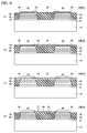
- FIG. 3 is a plan view of the elastic wave device according to the first embodiment.
- FIG. 2 is a sectional view taken along the line II-II of the elastic wave device of FIG. 1.
- FIG. 9 is a cross-sectional view of an elastic wave device according to a second embodiment.
- FIG. 13 is a cross-sectional view of an elastic wave device according to a third embodiment. It is a figure for explaining the 1st modification of a support layer. It is a figure for explaining the 2nd modification of a support layer. It is a figure for explaining the 3rd modification of a support layer.
- FIG. 5 is a diagram for describing a first example of a manufacturing process of the elastic wave device in FIG. 4.
- FIG. 5 is a diagram for describing a first example of a manufacturing process of the elastic wave device in FIG. 4.
- FIG. 11 is a diagram for explaining a second example of the manufacturing process of the elastic wave device in FIG. 4.
- FIG. 14 is a sectional view of an elastic wave device according to a fourth embodiment.
- FIG. 4 is a diagram illustrating an example of a shape of a wiring portion at a boundary portion between a piezoelectric thin film and a support layer.
- FIG. 15 is a sectional view of an elastic wave device according to a fifth embodiment.
- FIG. 19 is a diagram showing an elastic wave device according to a sixth embodiment.
- FIG. 15 is a cross-sectional view of an elastic wave device according to a modification of the sixth embodiment.
- FIG. 21 is a circuit diagram illustrating an example of a ladder-type filter according to a seventh embodiment.
- FIG. 16 is a schematic plan view of the elastic wave device of FIG. 15.
- FIG. 17 is a sectional view of a region RG1 in FIG. 16.
- FIG. 15 is a circuit diagram showing an example of a ladder-type filter according to an eighth embodiment.
- FIG. 19 is a cross-sectional view of the bridging capacitance section in FIG. 18.
- FIG. 19 is a schematic plan view of a portion of a region RG4 in FIG. 18.
- FIG. 21 is a schematic plan view of a ladder-type filter according to a ninth embodiment.
- FIG. 22 is a plan view of a portion of the series arm resonators S1 and S2 in FIG. 21.
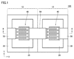
- FIG. 1 is a plan view of an elastic wave device 100 according to the first embodiment.
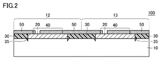
- FIG. 2 is a cross-sectional view taken along the line II-II of the elastic wave device 100 of FIG.
- the acoustic wave device 100 includes a support substrate 10 and resonating portions 12 and 13 formed adjacent to each other on the support substrate 10.
- the number of resonating units may be three or more.
- a case where a SAW filter is formed in the resonance unit will be described as an example, but the resonance unit may be formed of a BAW filter.
- the support substrate 10 is made of, for example, lithium tantalate (LiTaO 3 ), lithium niobate (LiNbO 3 ), a piezoelectric material such as quartz, alumina (Al 2 O 3 ), magnesia, silicon nitride (SiN), aluminum nitride (AlN). , Silicon carbide (SiC), zirconia (ZrO 2 ), cordierite, mullite, steatite, forsterite, and other ceramics; dielectrics such as glass; and semiconductors such as silicon (Si), sapphire, gallium nitride (GaN); A resin substrate or the like can be used.
- LiTaO 3 lithium tantalate
- LiNbO 3 lithium niobate
- a piezoelectric material such as quartz, alumina (Al 2 O 3 ), magnesia, silicon nitride (SiN), aluminum nitride (AlN).
- Each of the resonators 12 and 13 includes a piezoelectric thin film 20 and an elastic wave resonator formed of a comb-like electrode (IDT: Interdigital Transducer) 40 formed on the piezoelectric thin film 20.
- IDT Interdigital Transducer
- the piezoelectric thin film 20 and the IDT electrode 40 form a surface acoustic wave resonator (SAW filter).
- the piezoelectric thin film 20 is formed of, for example, a piezoelectric single crystal material such as lithium tantalate, lithium niobate, zinc oxide (ZnO), aluminum nitride, or lead zirconate titanate (PZT), or a piezoelectric laminated material thereof.
- the IDT electrode 40 is made of aluminum (Al), copper (Cu), silver (Ag), gold (Au), titanium (Ti), tungsten (W), platinum (Pt), chromium (Cr), nickel (Ni). ), Molybdenum (Mo), or a metal material such as an alloy containing these as a main component.
- the IDT electrode 40 may have a structure in which a plurality of metal films made of these metals or alloys are stacked.
- the periphery of the piezoelectric thin film 20 of the resonance parts 12 and 13 is surrounded by the support layer 30.
- the piezoelectric thin film 20 of the resonance unit 12 and the piezoelectric thin film 20 of the resonance unit 13 are divided by the support layer 30.
- the piezoelectric thin films 20 of the respective resonance parts 12 and 13 are arranged independently on the common support substrate 10.
- the support layer 30 is formed of a material having a smaller coefficient of linear expansion than the piezoelectric thin film 20, and for example, silicon dioxide (SiO 2 ) or polyimide (PI) is used.
- a wiring part 50 for electrically connecting the adjacent resonance parts 12, 13 is formed as necessary.
- reflectors may be arranged on both sides of the IDT electrode 40 on the piezoelectric thin film 20 (Y-axis direction in FIG. 1).
- the convex portion 35 is formed by filling the concave portion formed on the support substrate 10 with the material of the support layer 30 in the manufacturing process of the acoustic wave device 100.
- the protrusions 35 can suppress shrinkage that occurs when the polyimide is cured in the manufacturing process, and cracks occur between the piezoelectric thin film 20 and the support layer 30. Can be prevented.
- the piezoelectric thin films 20 of the adjacent resonance parts 12 and 13 are divided by the support layer 30 having a smaller linear expansion coefficient than the piezoelectric thin film 20. Therefore, even when a temperature difference occurs between the piezoelectric thin films 20 of the two resonance portions 12 and 13, the deformation of one of the piezoelectric thin films is prevented from affecting the other piezoelectric thin film by the surrounding support layer 30. be able to. Thereby, deterioration of the TCF characteristics can be suppressed.
- the piezoelectric thin film 20 of each resonance unit is directly arranged on the support substrate 10. However, if the piezoelectric thin film 20 is divided, the distance between the piezoelectric thin film 20 and the support substrate 10 can be reduced. May be provided with another layer.
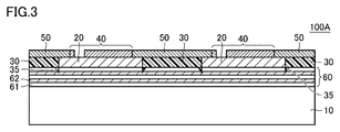
- FIG. 3 is a cross-sectional view of elastic wave device 100A according to the second embodiment.
- the elastic wave device 100A is different from the elastic wave device 100 of the first embodiment in that an intermediate layer 60 is provided between the piezoelectric thin film 20 and the support layer 30 and the support substrate 10.
- the protrusion 35 in the support layer 30 is located in the intermediate layer 60.
- the intermediate layer 60 includes at least the high sound velocity layer 62 that propagates an elastic bulk wave faster than the velocity of the elastic wave propagating to the piezoelectric thin film 20.
- the high sound velocity layer 62 include a DLC (Diamond-like Carbon) film, a piezoelectric material such as aluminum nitride, aluminum oxide, silicon carbide, silicon nitride, silicon, sapphire, lithium tantalate, lithium niobate, quartz, alumina, and zirconia.
- the high sound velocity layer 62 can effectively confine the energy of the elastic wave excited from the IDT electrode 40 to the piezoelectric thin film 20 in the piezoelectric thin film 20.
- the intermediate layer 60 includes, in addition to the high sonic layer 62, the low sonic layer 61, which is stacked on the high sonic layer 62 and propagates an elastic bulk wave lower in speed than the elastic wave propagating to the piezoelectric thin film 20. Further, the configuration may be provided.
- the low sound velocity layer 61 is made of, for example, silicon oxide, glass, silicon oxynitride, tantalum oxide, a compound obtained by adding fluorine, carbon, or boron to silicon oxide, or a material containing any of the above materials as a main component. Can be. 3 shows an example in which the intermediate layer 60 is formed as a laminate in which the low sound speed layers 61 and the high sound speed layers 62 are alternately stacked.
- the elastic wave is reflected at the interface between the low sound speed layer 61 and the high sound speed layer 62 or at the interface between the piezoelectric thin film 20 and the high sound speed layer 62, so that the acoustic wave is excited by the IDT electrode 40.
- the energy of the elastic wave can be effectively confined in the piezoelectric thin film 20 and the low sound speed layer 61.
- the thickness of the piezoelectric thin film 20 When the thickness of the piezoelectric thin film 20 is large, the influence of the material of the piezoelectric thin film 20 (for example, lithium tantalate) increases, so that elastic waves are not easily leaked in the thickness direction of the substrate. Is thicker, the effect of the linear expansion coefficient of the piezoelectric thin film 20 increases. Therefore, when the thickness of the piezoelectric thin film 20 increases, the TCF characteristics may deteriorate. Furthermore, since it becomes difficult to benefit from the support substrate 10 (for example, silicon) having high heat conductivity, TCF characteristics may be degraded.
- the support substrate 10 for example, silicon
- the thickness of the piezoelectric thin film 20 is preferably 3.5 ⁇ or less when the wavelength of the elastic wave determined from the electrode period of the IDT electrode 40 is ⁇ , and thus the Q value can be increased.
- the TCF characteristic can be improved by setting the thickness of the piezoelectric thin film 20 to 2.5 ⁇ or less, and the sound speed can be easily adjusted by setting the thickness to 1.5 ⁇ or less.
- the thickness of the low sound velocity layer 61 By setting the thickness of the low sound velocity layer 61 to 2.0 ⁇ or less, the film stress can be reduced, and the warpage of the substrate can be reduced. As a result, the yield rate of the acoustic wave device can be improved, and the characteristics can be stabilized.
- the high sound speed layer 62 is thin and the sound speed of the support substrate 10 is low, the surface acoustic waves are likely to leak to the support substrate 10. Then, the characteristics of the device may deteriorate due to the influence of the bulk radiation. As described above, since the function of confining the energy of the elastic wave in the piezoelectric thin film 20 and the low sound velocity layer 61 is exhibited by the high sound velocity layer 62, it is preferable that the thickness of the high sound velocity layer 62 be as large as possible.
- the intermediate layer 60 is provided with the high sonic layer.
- the support substrate 10 itself is formed of the high sonic layer material, and the intermediate layer 60 is formed of the low sonic layer material. Is also good.
- an intermediate layer 60 in which a high sound speed layer and a low sound speed layer are stacked may be provided between the support substrate 10 formed of the material of the high sound speed layer and the piezoelectric thin film 20.
- the intermediate layer 60 is composed of a high sonic layer and a low sonic layer determined by a relative velocity difference between the velocity of the elastic bulk wave propagating in each layer and the velocity of the elastic wave propagating in the piezoelectric thin film 20.
- a relative velocity difference between the velocity of the elastic bulk wave propagating in each layer and the velocity of the elastic wave propagating in the piezoelectric thin film 20 has been described, but another configuration can be adopted as a configuration for confining the energy of the elastic wave.
- the intermediate layer 60 may be configured such that layers having relatively different acoustic impedances are alternately stacked. That is, the portion of the low sound speed layer 61 in FIG. 3 is a low impedance layer (first layer) having a relatively low acoustic impedance, and the portion of the high sound speed layer 62 is a high impedance layer (the second layer) having a relatively high acoustic impedance. Layer). With such a configuration, since the elastic wave is reflected at the interface between the low impedance layer and the high impedance layer, the energy of the elastic wave excited by the IDT electrode 40 can be effectively confined in the piezoelectric thin film 20. Becomes possible.
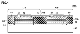
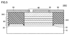
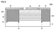
- FIG. 4 is a cross-sectional view of elastic wave device 100B according to the third embodiment.
- support layer 30B disposed around piezoelectric thin film 20 in each resonance portion extends to support substrate 10, and intermediate layer 60 is divided by support layer 30B. It is in a state. That is, in the intermediate layer 60, the portion between the piezoelectric thin film 20 of the first resonance section 12B and the support substrate 10 and the portion between the piezoelectric thin film 20 of the second resonance section 13B and the support substrate 10 are the first It is divided by a support layer 30B between the resonance part 12B and the second resonance part 13B.
- the protrusion 35 provided on the edge of the lower surface of the support layer 30 ⁇ / b> B is located in the support substrate 10.
- the configuration of the intermediate layer 60 is the same as that of the second embodiment, and may be a combination of a high sonic layer and a low sonic layer, or a combination of a high impedance layer and a low impedance layer. You may.
- the energy of the elastic wave excited by the IDT electrode 40 can be effectively confined in the piezoelectric thin film 20 by the intermediate layer 60.
- the position of the lower surface of the support layer 30B that divides the intermediate layer 60 does not necessarily have to coincide with the boundary between the support substrate 10 and the intermediate layer 60 as shown in FIG.
- the lower surface of the support layer 30C may be located closer to the intermediate layer 60 than the boundary between the support substrate 10 and the intermediate layer 60. In this case, the damage to the support substrate 10 can be reduced by preventing the protrusion 35 from being inside the support substrate 10.
- the lower surface of the support layer 30D may be positioned in the direction (first direction) closer to the support substrate 10 than the boundary between the support substrate 10 and the intermediate layer 60.
- the interface between the support substrate 10 and the high sound speed layer 62 It is known that a layer (charge generation layer 15) in which charges are generated is formed.
- the support layer 30E by adopting polyimide as the support layer 30E and arranging such that the lower surface thereof is closer to the support substrate 10 than the boundary between the support substrate 10 and the intermediate layer 60, the charge accumulated in the charge generation layer 15 is obtained. Can be effectively suppressed from moving to the adjacent resonance part.
- FIG. 8 is an example of a manufacturing process for forming the IDT electrode 40 before forming the support layer 30B
- FIG. 9 is an example of a manufacturing process for forming the IDT electrode 40 after forming the support layer 30B.
- a support substrate 10, an intermediate layer 60, and a piezoelectric thin film 20 are prepared, and the support substrate 10 and the piezoelectric thin film 20 are bonded together via the intermediate layer 60 to form an elastic wave device.
- a substrate having a basic structure is formed.
- the intermediate layer 60 is formed from the high sonic layer and the low sonic layer prior to the process of FIG. Process to be added.
- an IDT electrode 40 is formed on the surface of the piezoelectric thin film 20 on the substrate formed in FIG. 8A (FIG. 8B).
- other functional elements for example, capacitors, reflectors, etc.
- the functional element such as the IDT electrode 40 is formed on the piezoelectric thin film 20
- a portion where the piezoelectric thin film 20 and the intermediate layer 60 are left on the substrate surface is subjected to dry etching after masking, as shown in FIG.
- the portion of the piezoelectric thin film 20 and the intermediate layer 60 where the support layer 30B is to be formed is removed.
- the concave portion 75 is formed in the support substrate 10 by performing dry etching while covering the portion other than the portion where the concave portion 75 is to be formed with the resist.
- the position of the lower surface of the support layer is adjusted according to the degree of execution of the etching in FIG. 8C, as shown in FIGS.
- the support layer 30B is formed by filling the opening 70 formed by etching with, for example, polyimide.
- silicon dioxide (SiO 2 ) is used as the support layer 30B
- the support layer 30B is formed by a film forming process.
- the recess 75 formed in FIG. 8C is filled with the material of the support layer 30B to form the protrusion 35 of the support layer 30B (FIG. 8D).
- the opening 70 formed by removing the piezoelectric thin film 20 and the intermediate layer 60 is filled with a material for the support layer to form the support layer 30B (FIG. 9C). Then, a functional element such as the IDT electrode 40 is formed (FIG. 9D).
- the acoustic wave device 100B is formed by forming the wiring portion 50 on the support layer 30B (FIG. 9E).
- FIG. 10 is a cross-sectional view of an elastic wave device 100F formed in a WLP (Wafer Level Package) structure according to the fourth embodiment.
- WLP Wafer Level Package
- three resonating portions are formed on the supporting substrate 10, and the piezoelectric thin film 20 and the intermediate layer 60 of each resonating portion are divided by the supporting layer 30F.
- the support layer 30F of the elastic wave device 100F has a structure in which the height of the surface opposite to the support substrate 10 side is higher than the piezoelectric thin film 20, and the surface thereof partially overlaps the surface of the piezoelectric thin film 20. I have.
- a resin such as polyimide
- thermal contraction occurs due to a difference in linear expansion coefficient between the piezoelectric thin film 20 and the support layer 30F, the intermediate layer 60, and the piezoelectric layer.
- a gap may be generated between the thin film 20 and the thin film 20.
- by forming a structure in which a part of the support layer 30F overlaps the surface of the piezoelectric thin film 20 it is possible to prevent the generation of the void. As a result, disconnection of the wiring portion 50F formed on the upper surface of the support layer 30F can be prevented.
- a support member 80 for supporting the upper cover portion 90 is formed in the outermost support layer 30F in order to form the WLP structure.
- the support member 80 is made of a resin such as polyimide, and is arranged so as to surround the entirety of the plurality of resonance units provided therein.
- the cover 90 is made of, for example, a resin such as epoxy or a material such as insulating ceramic.
- the support member 80 and the cover 90 form an internal space in which the resonance unit including the ITD electrode 40 can vibrate. .
- a support member 82 for supporting the cover unit 90 is provided on the support layer 30F that divides the resonance unit.
- the support member 82 prevents the internal space from being crushed due to the deformation of the cover 90.
- the support member 80 and the cover portion 90 are formed with through-holes extending to the wiring portion 50F formed on the upper surface of the outermost support layer 30F, and the through-holes are filled with the under bump metal 95.
- the under bump metal 95 for example, a conductor such as Au, Ag, Cu, or Ni is used.
- a solder bump 96 is connected to the under bump metal 95, and the resonance unit and the external device are electrically connected via the under bump metal 95 and the solder bump 96.
- Such an elastic wave device 100F may be entirely molded with resin or the like after being mounted on an external substrate or the like. In such a case, pressure is applied to the cover 90 from the outside, so that the cover 90 is easily deformed. As described above, the deformation of the cover portion 90 is suppressed by providing the support member 82 on the support layer 30F that divides the resonance section. However, the thickness of the support layer 30F on which the support member 82 is provided (see FIG. 10). HB) is larger than the thickness of the outermost support layer 30F (HA in FIG. 10) (HA ⁇ HB), and the height of the cover 90 near the center of the elastic wave device 100F is changed to the cover of the outer periphery. By making the cover 90 higher than the height of the cover 90 (ie, making the cover 90 convex), the durability against external pressure can be further increased.
- the thickness of the support layer 30F on which the support member 82 is provided be thicker than the thickness of the outermost support layer 30F.
- the thickness may be set, or conversely, the thickness of the outermost support layer 30F may be increased.
- a part of the support layer 30F has a shape overlapping with the surface of the piezoelectric thin film 20 in order to prevent disconnection of the wiring part 50F, but by devising the shape of the wiring part, Further, the stress applied to the wiring portion can be reduced.
- a protrusion 55 is formed in the wiring portion 50G at a portion located at the boundary between the support layer 30G and the piezoelectric thin film 20.
- the shape of the protruding portion 55 is more preferably a curved shape as shown in FIG. 11 than a rectangular shape. With the curved shape, stress applied to the boundary between the support layer 30G and the piezoelectric thin film 20 and the portion where the protrusion 55 overlaps can be reduced.
- the shape of the wiring portion 50G shown in FIG. 11 can be applied to the first to third embodiments.
- the high impedance layer having a relatively high acoustic impedance and the low impedance layer having a relatively low acoustic impedance are alternately laminated as an intermediate layer for reflecting elastic waves, the high impedance layer is formed.
- tungsten (W), tantalum (Ta), niobium (Nb), or platinum (Pt) is used as a material.
- Tungsten, tantalum, niobium and platinum are materials that can cause migration due to moisture or outside air. When migration occurs, a part of the high-impedance layer is deficient and elastic waves cannot be appropriately reflected, and the characteristics of the elastic wave device may be changed.
- a description will be given of a configuration in which a protective layer is disposed on an elastic wave device to suppress migration of a high impedance layer in an intermediate layer.
- FIG. 12 is a cross-sectional view of elastic wave device 100H according to the fifth embodiment.
- FIGS. 12A to 12D show variations of the arrangement of the protective layer.
- the protective layer for example, a material such as silicon oxide or silicon nitride is used.
- the protective layer 76 covers the side surface of the laminated body of the support substrate 10, the intermediate layer 60 and the piezoelectric thin film 20, and the surface of the piezoelectric thin film 20 on which the IDT electrode 40 is formed. It is formed as follows. Such a configuration is realized by laminating the protective layer 76 before the step of forming the support layer 30B (between FIG. 8C and FIG. 8D) in the manufacturing process described with reference to FIG. Is done.
- the support layer 30 and the intermediate layer 60 are separated from each other by the protective layer 76, and the surface of the piezoelectric thin film 20 is shielded from the outside air. Therefore, the protection layer 76 can prevent moisture or the like that has passed through the support layer 30 or the piezoelectric thin film 20 from reaching the high impedance layer 62. This can suppress the occurrence of migration in the material forming the high impedance layer 62.
- a protective layer 76 is formed so as to cover the surfaces of the support layer 30 and the piezoelectric thin film 20. Then, the wiring portion 50 is formed on the upper surface of the protective layer 76 (the surface of the protective layer 76 opposite to the side of the piezoelectric thin film 20). The wiring section 50 is connected to the IDT electrode 40 arranged on the piezoelectric thin film 20 by an opening formed in the protective layer 76.
- Such a configuration is realized by laminating the protective layer 76 after the step of FIG. 8D or FIG. 9D.
- the support layer 30 and the piezoelectric thin film 20 are prevented from being exposed to the outside air, and the permeation of moisture into the support layer 30 and the piezoelectric thin film 20 can be prevented. Therefore, it is possible to suppress migration from occurring in the material forming the high impedance layer 62.
- the wiring portion 50 is also covered by the protective layer.
- Such a configuration is realized by laminating the protective layer 76 after the step of FIG. 8E or FIG. 9E.
- the wiring portion 50 is also covered by the protective layer 76. Therefore, like the elastic wave devices 100H1 and 100H2, an opening is formed in the protective layer 76 to allow the wiring portion 50 to pass therethrough. No need to form. Therefore, it is possible to further suppress the moisture from reaching the high impedance layer 62 through the opening. This can suppress the occurrence of migration in the material forming the high impedance layer 62.
- the protective layer 77 is formed only at the boundary between the high impedance layer 62 (second layer) and the support layer 30 in the intermediate layer 60.
- the protective layer 77 may be formed by forming a material such as silicon oxide or silicon nitride on the end of the high impedance layer 62 as in the first to third examples described above.
- the tungsten may be formed by oxidizing or nitriding an end portion of the tungsten.
- Embodiment 6 In each of the above embodiments, the configuration of the acoustic wave device in which a pair of adjacent resonance units are connected by the wiring unit has been described.
- FIG. 13 shows an elastic wave device 100J1 according to the sixth embodiment.
- the upper part (FIG. 13A) shows a plan view of the acoustic wave device 100J1
- the lower part shows a cross-sectional view taken along the XIII-XIII plane in the plan view. It is shown.
- elastic wave device 100J1 includes four IDT electrodes 41 to 44 arranged on piezoelectric thin film 20, and a resonance section is formed for each IDT electrode.
- the piezoelectric thin film 20 is disposed on the support substrate 10 with the intermediate layer 60 interposed therebetween, and the IDT electrode is formed on the piezoelectric thin film 20.
- the four resonance units are adjacent to each other via the common support layer 30G. More specifically, IDT electrode 41 and IDT electrode 42 are adjacent to each other in the X-axis direction via support layer 30G, and IDT electrode 43 and IDT electrode 44 are in the Y-axis direction via support layer 30G. Is adjacent to
- the wiring portions for connecting the IDT electrodes are mutually connected. Will cross. In this case, if the two wiring portions are arranged on the same plane, the wiring portions are short-circuited, so that it is necessary to largely bypass one of the wiring portions. Then, the area of the entire elastic wave device increases, which may be a factor that hinders downsizing of devices formed by the elastic wave device.
- the two wiring portions when two wiring portions intersect, the two wiring portions are formed in different layers in the intersection region and are arranged three-dimensionally, so that the size of the elastic wave device is increased. Insulation between the wiring parts is ensured while suppressing.
- the metal layer 85 is formed inside the support layer 30G, and the wiring portions 51 and 52 formed on the surface of the support layer 30G.
- the IDT electrode 41 and the IDT electrode 42 are connected by the and the metal layer 85.
- the IDT electrode 43 and the IDT electrode 44 are connected by a wiring portion 53 formed in a region between the wiring portion 51 and the wiring portion 52 on the surface of the support layer 30G. That is, in a region where the path connecting the IDT electrode 41 and the IDT electrode 42 and the path connecting the IDT electrode 43 and the IDT electrode 44 intersect when the elastic wave device 100J1 is viewed in plan, the support layer 30G is formed. Insulated by the insulating material to be formed.
- FIG. 13 illustrates an example in which two wires connecting the IDT electrodes intersect
- the above configuration is not limited to the wires connecting the IDT electrodes, and two wires in the acoustic wave device are provided.
- the present invention can be applied to other portions where wirings intersect.
- the wiring extending from the IDT electrode to the terminal at the end of the circuit may intersect with another wiring, or the wiring extending from one IDT electrode may intersect.
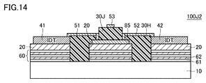
- FIG. 14 is a cross-sectional view of an elastic wave device 100J2 according to a modification of the sixth embodiment.
- the metal layer 85 is formed inside the support layer 30G.
- the metal layer 85 is formed on the intermediate layer 60 similarly to the resonance part.
- a metal layer 85 is formed on the piezoelectric thin film 20 thus formed.
- a support layer 30H is disposed around the intermediate layer 60 on which the metal layer 85 is formed, and the IDT electrodes are adjacent to each other via the support layer 30H.
- the IDT electrode 41 and the IDT electrode 42 are connected by wiring portions 51 and 52 formed on the surface of the support layer 30H and the metal layer 85, similarly to the elastic wave device 100J1.
- a support layer 30J is disposed above the metal layer 85, and a wiring portion 53 for connecting the IDT electrode 43 and the IDT electrode 44 is formed on the surface of the support layer 30J.
- the intersection region of the wiring portions can be arranged three-dimensionally, so that the insulation between the wiring portions can be suppressed while suppressing the size of the elastic wave device from increasing. Can be secured.
- an intersection region including the metal layer 85 can be simultaneously formed in the manufacturing process of the resonance section. Thereby, an additional step for forming the intersection region can be reduced.
- Embodiment 7 In some cases, a metal film is used as the high impedance layer of the intermediate layer. At this time, if the metal film is arranged to face the wiring portion, a capacitor is formed between the wiring portion and the metal film. In the case of an SMR (Solidly Mounted Resonator) type resonator in which high impedance layers and low impedance layers are alternately arranged, a metal film is formed at a position facing the IDT electrode in order to reflect an elastic wave in the intermediate layer. You. Therefore, when the metal layer disposed to face the wiring portion and the metal layer disposed to face the IDT electrode are electrically connected, a state in which a capacitor is connected in parallel to the SAW resonator can be obtained. .
- SMR Solidly Mounted Resonator
- the elastic wave device is a ladder-type filter having a series arm circuit and a parallel arm circuit
- filter characteristics may be affected depending on a resonator to which a capacitor is connected in parallel.
- FIG. 15 is a circuit diagram showing an example of a ladder-type filter 200 (hereinafter, also simply referred to as “filter 200”) according to the seventh embodiment.
- FIG. 16 is a schematic plan view of the elastic wave device (filter) shown in FIG.
- filter 200 includes a series arm circuit 201 connected between input terminal IN and output terminal OUT, and a parallel arm connected between series arm circuit 201 and ground potential. And a circuit 202.
- the series arm circuit 201 includes series arm resonators S1 to S3 connected in series between the input terminal IN and the output terminal OUT.
- the parallel arm circuit 202 includes parallel arm resonators P1 and P2.
- the parallel arm resonator P1 is connected between a connection node between the series arm resonators S1 and S2 and a ground potential.
- the parallel arm resonator P2 is connected between a connection node between the series arm resonators S2 and S3 and a ground potential.
- the configuration of the series arm circuit 201 and the parallel arm circuit 202 in the filter 200 is not limited to the configuration shown in FIG. 15, but may be another configuration.
- the series arm resonator and the parallel arm resonator correspond to the resonance unit in the above-described embodiment.
- the resonance frequency Frs of the series arm resonator and the anti-resonance frequency Fap of the parallel arm resonator are set near the center frequency of the target pass band, so that the parallel arm resonator A bandpass filter having a pass band between a resonance frequency Frp and an anti-resonance frequency Fap of the series arm resonator is formed.
- the specific band (Fa ⁇ Fr) / Fr).
- steepness of the attenuation characteristic between the pass band and the attenuation band may be required in order to increase the S / N ratio. It is generally known that reducing the bandwidth is effective for improving the steepness.
- the attenuation pole on the higher side of the pass band is determined by the series arm resonator. Therefore, in order to achieve a wider pass band and sharper attenuation characteristics on the high frequency side, it is effective to reduce the fractional band for the series arm resonator and increase the fractional band for the parallel arm resonator. It becomes.
- each resonator when the metal film 65 is provided on the high-impedance layer 62 of the intermediate layer 60, a capacitor is connected in parallel to the resonator (for example, C1, C2 in FIG. 15).
- the anti-resonance frequency moves to a lower frequency side, so that the fractional band generally becomes smaller. Therefore, it is preferable to reduce the influence of the metal film for the parallel arm resonator for which it is desired to increase the bandwidth.
- FIG. 17 is a cross-sectional view of a portion of region RG1 including series arm resonator S2 and parallel arm resonator P1 of FIG. 16 in elastic wave device 100K according to the seventh embodiment.
- elastic wave device 100K has a configuration in which piezoelectric thin film 20 and support layer 30 are formed on intermediate layer 60 as shown in FIG. 62 includes a metal film 65.
- the position where the metal film 65 is included in the intermediate layer 60 is not limited to the uppermost high impedance layer 62.
- the metal film 65 may be arranged at any one of the layers constituting the intermediate layer 60 or at the interface between two adjacent layers.
- the left resonating part corresponds to the series arm resonator S2, and the right resonating part corresponds to the parallel arm resonator P1.
- the metal film 65 is formed over the piezoelectric thin film 20 and the support layer 30 in the intermediate layer 60A.
- the parallel arm resonator P ⁇ b> 1 the metal film 65 is formed in a portion facing the IDT electrode 40, but the metal film 65 is not formed in a portion facing the wiring portion 50. That is, when the elastic wave device 100K is viewed in a plan view, the wiring portion 50 and the metal film 65 do not overlap in the parallel arm resonator P1.
- the support layer 30 extends from the wiring portion 50 to the support substrate 10 without providing the intermediate layer 60A between the wiring portion 50 of the parallel arm resonator P1 and the support substrate 10. There may be.
- the metal film 65 is not formed on all the portions facing the wiring portion 50.
- the metal film 65 is formed on a portion of the parallel arm resonator P ⁇ b> 1 facing the wiring portion 50. Is also good.
- the wiring portion 50 and the metal film 65 face each other via the support layer 30 made of an insulating material, and a capacitor is formed in this portion. Then, a path (arrow AR1 in FIG. 17) from the input side IDT electrode of the series arm resonator S2 to the output side IDT electrode through the metal film 65 is formed, and the IDT electrode 40 of the series arm resonator S2 is formed.
- the configuration is such that the capacitors are connected in parallel.
- the wiring section 50 is not formed in the portion (region RG3) facing the wiring section 50, the wiring section 50 such as the series arm resonator S2 and the wiring section 50 are not formed. Does not occur. Therefore, a capacitor connected in parallel to the IDT electrode 40 of the parallel arm resonator P1 is not formed.
- the elastic wave device of the ladder type filter in which the metal film is used as the high impedance layer of the intermediate layer when the elastic wave device is viewed in a plan view, the wiring portion connected to the parallel arm resonator and the metal film are separated. By adopting a configuration that does not overlap, the influence on the filter characteristics can be reduced.
- Embodiment 8 As described in the seventh embodiment, in the ladder-type filter, by connecting a capacitor in parallel with the series arm resonator to reduce the fractional band of the series arm resonator, the bandwidth of the band-pass filter is increased. The steepness of the attenuation characteristic on the side can be increased.
- FIG. 18 is a circuit diagram showing an example of ladder-type filter 200A according to the eighth embodiment.
- the filter 200A has a configuration in which a bridging capacitor C10 is connected in parallel to the series arm resonator S1 in addition to the configuration of the filter 200 of the seventh embodiment.
- the bridge capacitance section C10 of the filter 200A has the same configuration as each resonator (resonance section) included in the series arm circuit 201 and the parallel arm circuit 202.
- the bridging capacitor C10 has a configuration in which the IDT electrode 40A is formed on the piezoelectric thin film 20 laminated on the intermediate layer 60A.
- the electrode fingers of the IDT electrode 40A of the bridging capacitance portion C10 are arranged so as to be parallel to the propagation direction of the surface acoustic wave. I have. Therefore, the IDT electrode 40A does not excite with a surface acoustic wave and functions as a capacitor.
- the metal film 65 is disposed on the uppermost high impedance layer 62 of the intermediate layer 60A of the bridging capacitor C10 so as to face the piezoelectric thin film 20 and the support layer 30.
- the configuration is such that the capacitor C0 is connected in parallel to the IDT electrode 40A forming the bridging capacitance portion C10.
- the capacitance of the bridging capacitance portion C10 can be reduced by using the capacitor C0 formed by the metal film 65 of the intermediate layer 60A. Since the capacitance of the bridging capacitor C10 is determined by the size of the IDT electrode 40A, the size of the bridging capacitor C10 can be reduced as a result.
- FIG. 18 illustrates an example of a configuration in which the bridging capacitance portion is disposed with respect to the series arm resonator S1, instead of or in addition to this, the series arm resonator S2 and / or the series arm resonator may be arranged.
- a bridging capacitance section may be provided in S3.
- Embodiment 9 As described in the seventh and eighth embodiments, in the configuration in which the metal film is provided on the high impedance layer of the intermediate layer in the ladder-type filter, the wiring portion and the metal film are opposed to each other so as to be connected to the resonator in parallel. Capacitor can be formed.
- the fractional band of the series arm resonator can be adjusted. Therefore, in the ninth embodiment, a configuration in which the capacitance of the capacitor connected in parallel for each series arm resonator can be adjusted by adjusting the area where the wiring portion and the metal film overlap each other for each series arm resonator. explain.
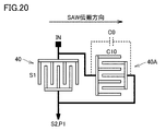
- FIG. 21 is a schematic plan view of a ladder-type filter 200B according to the ninth embodiment.
- the filter 200B has a circuit basically similar to the circuit diagram shown in FIG. 15 of the seventh embodiment, and is configured by series arm resonators S1 to S3 and parallel arm resonators P1 and P2. I have.
- FIG. 22 is a plan view of an elastic wave device 100L corresponding to the series arm resonators S1 and S2 in the filter 200B.
- the metal film 65 is disposed on the high impedance layer of the intermediate layer so as to face the wiring portions on the input side and the output side of each series arm resonator (FIG. 22).
- the capacitor C11 is formed between the input side wiring portion 56 and the output side wiring portion 57.
- a capacitor C12 is formed between the input side wiring portion 57 and the output side wiring portion 58.
- a capacitor C13 is formed between the input side wiring portion 58 and the output side wiring portion 59.
- the capacitance of the capacitor formed by each wiring portion and the metal film 65 can be adjusted by changing the area where the metal film 65 overlaps the input-side and output-side wiring portions forming the capacitor.
- the capacitance of the capacitor can be changed by adjusting the line width of each wiring portion.
- the line width of the wiring portion may be fixed, and the width of the metal film 65 facing each wiring portion may be individually changed.
- the input-side wiring portion indicates a wiring portion connected to the input-side bus bar of the IDT electrode in each resonator, and the output-side wiring portion corresponds to the output-side bus bar of the IDT electrode in each resonator. The wiring part to be connected is shown.
- the fractional band can be adjusted for each series arm resonator. Therefore, the degree of freedom in designing a ladder-type filter can be increased.
Landscapes
- Physics & Mathematics (AREA)
- Acoustics & Sound (AREA)
- Engineering & Computer Science (AREA)
- Manufacturing & Machinery (AREA)
- Surface Acoustic Wave Elements And Circuit Networks Thereof (AREA)
Priority Applications (2)
| Application Number | Priority Date | Filing Date | Title |
|---|---|---|---|
| CN201980042056.4A CN112385144A (zh) | 2018-07-03 | 2019-07-02 | 弹性波装置 |
| US17/102,468 US20210111697A1 (en) | 2018-07-03 | 2020-11-24 | Acoustic wave device |
Applications Claiming Priority (2)
| Application Number | Priority Date | Filing Date | Title |
|---|---|---|---|
| JP2018127006 | 2018-07-03 | ||
| JP2018-127006 | 2018-07-03 |
Related Child Applications (1)
| Application Number | Title | Priority Date | Filing Date |
|---|---|---|---|
| US17/102,468 Continuation US20210111697A1 (en) | 2018-07-03 | 2020-11-24 | Acoustic wave device |
Publications (1)
| Publication Number | Publication Date |
|---|---|
| WO2020009121A1 true WO2020009121A1 (ja) | 2020-01-09 |
Family
ID=69059668
Family Applications (1)
| Application Number | Title | Priority Date | Filing Date |
|---|---|---|---|
| PCT/JP2019/026346 WO2020009121A1 (ja) | 2018-07-03 | 2019-07-02 | 弾性波装置 |
Country Status (3)
| Country | Link |
|---|---|
| US (1) | US20210111697A1 (zh) |
| CN (1) | CN112385144A (zh) |
| WO (1) | WO2020009121A1 (zh) |
Cited By (2)
| Publication number | Priority date | Publication date | Assignee | Title |
|---|---|---|---|---|
| WO2021200677A1 (ja) * | 2020-03-31 | 2021-10-07 | 株式会社村田製作所 | 弾性波装置 |
| WO2022138827A1 (ja) * | 2020-12-25 | 2022-06-30 | 株式会社村田製作所 | フィルタ装置 |
Citations (13)
| Publication number | Priority date | Publication date | Assignee | Title |
|---|---|---|---|---|
| JPH06152317A (ja) * | 1992-11-13 | 1994-05-31 | Murata Mfg Co Ltd | 梯子型弾性表面波フィルタ |
| JP2002198777A (ja) * | 2000-11-24 | 2002-07-12 | Nokia Mobile Phones Ltd | 圧電共振子を含むフィルタ構造および構成 |
| JP2004343735A (ja) * | 2003-04-25 | 2004-12-02 | Matsushita Electric Ind Co Ltd | アンテナ共用器、アンテナ共用器の設計方法、アンテナ共用器の生産方法、及びそれを用いた通信装置 |
| JP2008211394A (ja) * | 2007-02-23 | 2008-09-11 | Matsushita Electric Works Ltd | 共振装置 |
| WO2009157587A1 (ja) * | 2008-06-27 | 2009-12-30 | 京セラ株式会社 | 弾性波装置 |
| JP2010098385A (ja) * | 2008-10-14 | 2010-04-30 | Murata Mfg Co Ltd | 弾性波装置 |
| JP2013009173A (ja) * | 2011-06-24 | 2013-01-10 | Denso Corp | 弾性表面波デバイス |
| WO2015098678A1 (ja) * | 2013-12-27 | 2015-07-02 | 株式会社村田製作所 | 弾性波装置 |
| WO2016208426A1 (ja) * | 2015-06-25 | 2016-12-29 | 株式会社村田製作所 | 弾性波装置 |
| JP2017152870A (ja) * | 2016-02-23 | 2017-08-31 | 太陽誘電株式会社 | 弾性波デバイス |
| WO2018003283A1 (ja) * | 2016-07-01 | 2018-01-04 | 株式会社村田製作所 | 弾性波装置及び電子部品 |
| WO2018061436A1 (ja) * | 2016-09-27 | 2018-04-05 | 株式会社村田製作所 | 弾性波装置、高周波フロントエンド回路及び通信装置 |
| WO2018096783A1 (ja) * | 2016-11-22 | 2018-05-31 | 株式会社村田製作所 | 弾性波装置、フロントエンド回路および通信装置 |
Family Cites Families (1)
| Publication number | Priority date | Publication date | Assignee | Title |
|---|---|---|---|---|
| JP6791390B2 (ja) * | 2017-08-29 | 2020-11-25 | 株式会社村田製作所 | 弾性波装置、高周波フロントエンド回路及び通信装置 |
-
2019
- 2019-07-02 CN CN201980042056.4A patent/CN112385144A/zh active Pending
- 2019-07-02 WO PCT/JP2019/026346 patent/WO2020009121A1/ja active Application Filing
-
2020
- 2020-11-24 US US17/102,468 patent/US20210111697A1/en active Pending
Patent Citations (13)
| Publication number | Priority date | Publication date | Assignee | Title |
|---|---|---|---|---|
| JPH06152317A (ja) * | 1992-11-13 | 1994-05-31 | Murata Mfg Co Ltd | 梯子型弾性表面波フィルタ |
| JP2002198777A (ja) * | 2000-11-24 | 2002-07-12 | Nokia Mobile Phones Ltd | 圧電共振子を含むフィルタ構造および構成 |
| JP2004343735A (ja) * | 2003-04-25 | 2004-12-02 | Matsushita Electric Ind Co Ltd | アンテナ共用器、アンテナ共用器の設計方法、アンテナ共用器の生産方法、及びそれを用いた通信装置 |
| JP2008211394A (ja) * | 2007-02-23 | 2008-09-11 | Matsushita Electric Works Ltd | 共振装置 |
| WO2009157587A1 (ja) * | 2008-06-27 | 2009-12-30 | 京セラ株式会社 | 弾性波装置 |
| JP2010098385A (ja) * | 2008-10-14 | 2010-04-30 | Murata Mfg Co Ltd | 弾性波装置 |
| JP2013009173A (ja) * | 2011-06-24 | 2013-01-10 | Denso Corp | 弾性表面波デバイス |
| WO2015098678A1 (ja) * | 2013-12-27 | 2015-07-02 | 株式会社村田製作所 | 弾性波装置 |
| WO2016208426A1 (ja) * | 2015-06-25 | 2016-12-29 | 株式会社村田製作所 | 弾性波装置 |
| JP2017152870A (ja) * | 2016-02-23 | 2017-08-31 | 太陽誘電株式会社 | 弾性波デバイス |
| WO2018003283A1 (ja) * | 2016-07-01 | 2018-01-04 | 株式会社村田製作所 | 弾性波装置及び電子部品 |
| WO2018061436A1 (ja) * | 2016-09-27 | 2018-04-05 | 株式会社村田製作所 | 弾性波装置、高周波フロントエンド回路及び通信装置 |
| WO2018096783A1 (ja) * | 2016-11-22 | 2018-05-31 | 株式会社村田製作所 | 弾性波装置、フロントエンド回路および通信装置 |
Cited By (2)
| Publication number | Priority date | Publication date | Assignee | Title |
|---|---|---|---|---|
| WO2021200677A1 (ja) * | 2020-03-31 | 2021-10-07 | 株式会社村田製作所 | 弾性波装置 |
| WO2022138827A1 (ja) * | 2020-12-25 | 2022-06-30 | 株式会社村田製作所 | フィルタ装置 |
Also Published As
| Publication number | Publication date |
|---|---|
| US20210111697A1 (en) | 2021-04-15 |
| CN112385144A (zh) | 2021-02-19 |
Similar Documents
| Publication | Publication Date | Title |
|---|---|---|
| US10469055B2 (en) | Filter device including longitudinally coupled resonator elastic wave filter and elastic wave resonator | |
| JP4587732B2 (ja) | 弾性表面波装置 | |
| US20100134210A1 (en) | Piezoelectric Resonator and Piezoelectric Filter Device | |
| US9847770B2 (en) | Elastic wave resonator, elastic wave filter apparatus, and duplexer | |
| JP6453913B2 (ja) | 弾性波装置、分波器および通信装置 | |
| JP6534366B2 (ja) | 弾性波デバイス | |
| US10756698B2 (en) | Elastic wave device | |
| US20220216846A1 (en) | Acoustic wave device | |
| US11764880B2 (en) | Acoustic wave device, multiplexer, high-frequency front end circuit, and communication device | |
| JP6427075B2 (ja) | 弾性波デバイス、分波器、及びモジュール | |
| EP1871007B1 (en) | Piezoelectric thin film filter | |
| US20220029601A1 (en) | Acoustic wave device | |
| CN111937305A (zh) | 弹性波元件、弹性波滤波器、分波器以及通信装置 | |
| JPWO2019131533A1 (ja) | 弾性波フィルタ、マルチプレクサ、高周波フロントエンド回路および通信装置 | |
| US20210111697A1 (en) | Acoustic wave device | |
| US20220239280A1 (en) | Acoustic wave filter | |
| JP2004153580A (ja) | 弾性表面波装置 | |
| JP7414080B2 (ja) | 弾性波デバイスおよびそれを備えたラダー型フィルタ | |
| JP2018129630A (ja) | 弾性波デバイス | |
| JP6947220B2 (ja) | フィルタ装置 | |
| JP2020191535A (ja) | 弾性波デバイス、フィルタおよびマルチプレクサ | |
| JP7421541B2 (ja) | フィルタおよびマルチフィルタ | |
| WO2023210524A1 (ja) | 弾性波素子及び通信装置 | |
| WO2023074373A1 (ja) | 弾性波共振子、弾性波フィルタ装置およびマルチプレクサ | |
| WO2023054301A1 (ja) | 弾性波フィルタ装置およびマルチプレクサ |
Legal Events
| Date | Code | Title | Description |
|---|---|---|---|
| 121 | Ep: the epo has been informed by wipo that ep was designated in this application |
Ref document number: 19830548 Country of ref document: EP Kind code of ref document: A1 |
|
| NENP | Non-entry into the national phase |
Ref country code: DE |
|
| 122 | Ep: pct application non-entry in european phase |
Ref document number: 19830548 Country of ref document: EP Kind code of ref document: A1 |
|
| NENP | Non-entry into the national phase |
Ref country code: JP |