WO2020009121A1 - 弾性波装置 - Google Patents
弾性波装置 Download PDFInfo
- Publication number
- WO2020009121A1 WO2020009121A1 PCT/JP2019/026346 JP2019026346W WO2020009121A1 WO 2020009121 A1 WO2020009121 A1 WO 2020009121A1 JP 2019026346 W JP2019026346 W JP 2019026346W WO 2020009121 A1 WO2020009121 A1 WO 2020009121A1
- Authority
- WO
- WIPO (PCT)
- Prior art keywords
- wave device
- layer
- elastic wave
- thin film
- piezoelectric thin
- Prior art date
Links
- 239000010409 thin film Substances 0.000 claims abstract description 119
- 239000000758 substrate Substances 0.000 claims abstract description 75
- 239000010410 layer Substances 0.000 claims description 291
- 229910052751 metal Inorganic materials 0.000 claims description 59
- 239000002184 metal Substances 0.000 claims description 59
- 239000010408 film Substances 0.000 claims description 43
- 239000011241 protective layer Substances 0.000 claims description 22
- VYPSYNLAJGMNEJ-UHFFFAOYSA-N Silicium dioxide Chemical compound O=[Si]=O VYPSYNLAJGMNEJ-UHFFFAOYSA-N 0.000 claims description 16
- 239000004642 Polyimide Substances 0.000 claims description 9
- 229920001721 polyimide Polymers 0.000 claims description 9
- 235000012239 silicon dioxide Nutrition 0.000 claims description 7
- XUIMIQQOPSSXEZ-UHFFFAOYSA-N Silicon Chemical compound [Si] XUIMIQQOPSSXEZ-UHFFFAOYSA-N 0.000 claims description 6
- 239000010703 silicon Substances 0.000 claims description 6
- 229910052710 silicon Inorganic materials 0.000 claims description 6
- 230000001902 propagating effect Effects 0.000 claims description 5
- 239000000377 silicon dioxide Substances 0.000 claims description 5
- 238000005121 nitriding Methods 0.000 claims description 2
- 230000001590 oxidative effect Effects 0.000 claims description 2
- 239000003990 capacitor Substances 0.000 description 31
- 239000000463 material Substances 0.000 description 29
- 238000004519 manufacturing process Methods 0.000 description 11
- 238000010586 diagram Methods 0.000 description 9
- 230000004048 modification Effects 0.000 description 8
- 238000012986 modification Methods 0.000 description 8
- BASFCYQUMIYNBI-UHFFFAOYSA-N platinum Chemical compound [Pt] BASFCYQUMIYNBI-UHFFFAOYSA-N 0.000 description 8
- 230000005012 migration Effects 0.000 description 7
- 238000013508 migration Methods 0.000 description 7
- 238000000034 method Methods 0.000 description 6
- 239000011347 resin Substances 0.000 description 6
- 229920005989 resin Polymers 0.000 description 6
- 238000010897 surface acoustic wave method Methods 0.000 description 6
- WFKWXMTUELFFGS-UHFFFAOYSA-N tungsten Chemical compound [W] WFKWXMTUELFFGS-UHFFFAOYSA-N 0.000 description 6
- 229910052721 tungsten Inorganic materials 0.000 description 6
- 239000010937 tungsten Substances 0.000 description 6
- 229910052581 Si3N4 Inorganic materials 0.000 description 5
- 230000008569 process Effects 0.000 description 5
- HQVNEWCFYHHQES-UHFFFAOYSA-N silicon nitride Chemical compound N12[Si]34N5[Si]62N3[Si]51N64 HQVNEWCFYHHQES-UHFFFAOYSA-N 0.000 description 5
- WSMQKESQZFQMFW-UHFFFAOYSA-N 5-methyl-pyrazole-3-carboxylic acid Chemical compound CC1=CC(C(O)=O)=NN1 WSMQKESQZFQMFW-UHFFFAOYSA-N 0.000 description 4
- CPLXHLVBOLITMK-UHFFFAOYSA-N Magnesium oxide Chemical compound [Mg]=O CPLXHLVBOLITMK-UHFFFAOYSA-N 0.000 description 4
- PXHVJJICTQNCMI-UHFFFAOYSA-N Nickel Chemical compound [Ni] PXHVJJICTQNCMI-UHFFFAOYSA-N 0.000 description 4
- MCMNRKCIXSYSNV-UHFFFAOYSA-N Zirconium dioxide Chemical compound O=[Zr]=O MCMNRKCIXSYSNV-UHFFFAOYSA-N 0.000 description 4
- 238000004891 communication Methods 0.000 description 4
- 238000001312 dry etching Methods 0.000 description 4
- 229910052814 silicon oxide Inorganic materials 0.000 description 4
- 239000000919 ceramic Substances 0.000 description 3
- 239000010949 copper Substances 0.000 description 3
- 239000010931 gold Substances 0.000 description 3
- 238000009413 insulation Methods 0.000 description 3
- 238000010030 laminating Methods 0.000 description 3
- GQYHUHYESMUTHG-UHFFFAOYSA-N lithium niobate Chemical compound [Li+].[O-][Nb](=O)=O GQYHUHYESMUTHG-UHFFFAOYSA-N 0.000 description 3
- 239000010955 niobium Substances 0.000 description 3
- 229910052697 platinum Inorganic materials 0.000 description 3
- 229910000679 solder Inorganic materials 0.000 description 3
- OKTJSMMVPCPJKN-UHFFFAOYSA-N Carbon Chemical compound [C] OKTJSMMVPCPJKN-UHFFFAOYSA-N 0.000 description 2
- 229910004298 SiO 2 Inorganic materials 0.000 description 2
- 239000000956 alloy Substances 0.000 description 2
- 229910045601 alloy Inorganic materials 0.000 description 2
- PNEYBMLMFCGWSK-UHFFFAOYSA-N aluminium oxide Inorganic materials [O-2].[O-2].[O-2].[Al+3].[Al+3] PNEYBMLMFCGWSK-UHFFFAOYSA-N 0.000 description 2
- 229910052799 carbon Inorganic materials 0.000 description 2
- 239000011651 chromium Substances 0.000 description 2
- 230000008602 contraction Effects 0.000 description 2
- 229910052802 copper Inorganic materials 0.000 description 2
- PMHQVHHXPFUNSP-UHFFFAOYSA-M copper(1+);methylsulfanylmethane;bromide Chemical compound Br[Cu].CSC PMHQVHHXPFUNSP-UHFFFAOYSA-M 0.000 description 2
- 229910052878 cordierite Inorganic materials 0.000 description 2
- JSKIRARMQDRGJZ-UHFFFAOYSA-N dimagnesium dioxido-bis[(1-oxido-3-oxo-2,4,6,8,9-pentaoxa-1,3-disila-5,7-dialuminabicyclo[3.3.1]nonan-7-yl)oxy]silane Chemical compound [Mg++].[Mg++].[O-][Si]([O-])(O[Al]1O[Al]2O[Si](=O)O[Si]([O-])(O1)O2)O[Al]1O[Al]2O[Si](=O)O[Si]([O-])(O1)O2 JSKIRARMQDRGJZ-UHFFFAOYSA-N 0.000 description 2
- KZHJGOXRZJKJNY-UHFFFAOYSA-N dioxosilane;oxo(oxoalumanyloxy)alumane Chemical compound O=[Si]=O.O=[Si]=O.O=[Al]O[Al]=O.O=[Al]O[Al]=O.O=[Al]O[Al]=O KZHJGOXRZJKJNY-UHFFFAOYSA-N 0.000 description 2
- 238000005530 etching Methods 0.000 description 2
- 229910052839 forsterite Inorganic materials 0.000 description 2
- 239000011521 glass Substances 0.000 description 2
- 229910052737 gold Inorganic materials 0.000 description 2
- 239000011810 insulating material Substances 0.000 description 2
- 229910052451 lead zirconate titanate Inorganic materials 0.000 description 2
- HCWCAKKEBCNQJP-UHFFFAOYSA-N magnesium orthosilicate Chemical compound [Mg+2].[Mg+2].[O-][Si]([O-])([O-])[O-] HCWCAKKEBCNQJP-UHFFFAOYSA-N 0.000 description 2
- 239000000395 magnesium oxide Substances 0.000 description 2
- 229910052863 mullite Inorganic materials 0.000 description 2
- 229910052758 niobium Inorganic materials 0.000 description 2
- GUCVJGMIXFAOAE-UHFFFAOYSA-N niobium atom Chemical compound [Nb] GUCVJGMIXFAOAE-UHFFFAOYSA-N 0.000 description 2
- 239000010453 quartz Substances 0.000 description 2
- 229910052594 sapphire Inorganic materials 0.000 description 2
- 239000010980 sapphire Substances 0.000 description 2
- HBMJWWWQQXIZIP-UHFFFAOYSA-N silicon carbide Chemical compound [Si+]#[C-] HBMJWWWQQXIZIP-UHFFFAOYSA-N 0.000 description 2
- 229910052709 silver Inorganic materials 0.000 description 2
- -1 steatite Chemical compound 0.000 description 2
- 229910052715 tantalum Inorganic materials 0.000 description 2
- GUVRBAGPIYLISA-UHFFFAOYSA-N tantalum atom Chemical compound [Ta] GUVRBAGPIYLISA-UHFFFAOYSA-N 0.000 description 2
- 239000010936 titanium Substances 0.000 description 2
- 229910018072 Al 2 O 3 Inorganic materials 0.000 description 1
- PIGFYZPCRLYGLF-UHFFFAOYSA-N Aluminum nitride Chemical compound [Al]#N PIGFYZPCRLYGLF-UHFFFAOYSA-N 0.000 description 1
- ZOXJGFHDIHLPTG-UHFFFAOYSA-N Boron Chemical compound [B] ZOXJGFHDIHLPTG-UHFFFAOYSA-N 0.000 description 1
- VYZAMTAEIAYCRO-UHFFFAOYSA-N Chromium Chemical compound [Cr] VYZAMTAEIAYCRO-UHFFFAOYSA-N 0.000 description 1
- RYGMFSIKBFXOCR-UHFFFAOYSA-N Copper Chemical compound [Cu] RYGMFSIKBFXOCR-UHFFFAOYSA-N 0.000 description 1
- 239000004593 Epoxy Substances 0.000 description 1
- PXGOKWXKJXAPGV-UHFFFAOYSA-N Fluorine Chemical compound FF PXGOKWXKJXAPGV-UHFFFAOYSA-N 0.000 description 1
- JMASRVWKEDWRBT-UHFFFAOYSA-N Gallium nitride Chemical compound [Ga]#N JMASRVWKEDWRBT-UHFFFAOYSA-N 0.000 description 1
- 229910013641 LiNbO 3 Inorganic materials 0.000 description 1
- ZOKXTWBITQBERF-UHFFFAOYSA-N Molybdenum Chemical compound [Mo] ZOKXTWBITQBERF-UHFFFAOYSA-N 0.000 description 1
- BQCADISMDOOEFD-UHFFFAOYSA-N Silver Chemical compound [Ag] BQCADISMDOOEFD-UHFFFAOYSA-N 0.000 description 1
- RTAQQCXQSZGOHL-UHFFFAOYSA-N Titanium Chemical compound [Ti] RTAQQCXQSZGOHL-UHFFFAOYSA-N 0.000 description 1
- XLOMVQKBTHCTTD-UHFFFAOYSA-N Zinc monoxide Chemical compound [Zn]=O XLOMVQKBTHCTTD-UHFFFAOYSA-N 0.000 description 1
- 229910052782 aluminium Inorganic materials 0.000 description 1
- XAGFODPZIPBFFR-UHFFFAOYSA-N aluminium Chemical compound [Al] XAGFODPZIPBFFR-UHFFFAOYSA-N 0.000 description 1
- 230000008901 benefit Effects 0.000 description 1
- 229910052796 boron Inorganic materials 0.000 description 1
- 230000008859 change Effects 0.000 description 1
- 229910052804 chromium Inorganic materials 0.000 description 1
- 150000001875 compounds Chemical class 0.000 description 1
- 239000004020 conductor Substances 0.000 description 1
- 239000013078 crystal Substances 0.000 description 1
- 230000002950 deficient Effects 0.000 description 1
- 230000006866 deterioration Effects 0.000 description 1
- 239000010432 diamond Substances 0.000 description 1
- 229910003460 diamond Inorganic materials 0.000 description 1
- 239000003989 dielectric material Substances 0.000 description 1
- 238000009826 distribution Methods 0.000 description 1
- 230000000694 effects Effects 0.000 description 1
- 239000011737 fluorine Substances 0.000 description 1
- 229910052731 fluorine Inorganic materials 0.000 description 1
- PCHJSUWPFVWCPO-UHFFFAOYSA-N gold Chemical compound [Au] PCHJSUWPFVWCPO-UHFFFAOYSA-N 0.000 description 1
- 239000002648 laminated material Substances 0.000 description 1
- HFGPZNIAWCZYJU-UHFFFAOYSA-N lead zirconate titanate Chemical compound [O-2].[O-2].[O-2].[O-2].[O-2].[Ti+4].[Zr+4].[Pb+2] HFGPZNIAWCZYJU-UHFFFAOYSA-N 0.000 description 1
- 230000000873 masking effect Effects 0.000 description 1
- 239000007769 metal material Substances 0.000 description 1
- 150000002739 metals Chemical class 0.000 description 1
- 239000000203 mixture Substances 0.000 description 1
- 229910052750 molybdenum Inorganic materials 0.000 description 1
- 239000011733 molybdenum Substances 0.000 description 1
- 229910052759 nickel Inorganic materials 0.000 description 1
- TWNQGVIAIRXVLR-UHFFFAOYSA-N oxo(oxoalumanyloxy)alumane Chemical compound O=[Al]O[Al]=O TWNQGVIAIRXVLR-UHFFFAOYSA-N 0.000 description 1
- BPUBBGLMJRNUCC-UHFFFAOYSA-N oxygen(2-);tantalum(5+) Chemical compound [O-2].[O-2].[O-2].[O-2].[O-2].[Ta+5].[Ta+5] BPUBBGLMJRNUCC-UHFFFAOYSA-N 0.000 description 1
- 230000005855 radiation Effects 0.000 description 1
- 239000004065 semiconductor Substances 0.000 description 1
- 229910010271 silicon carbide Inorganic materials 0.000 description 1
- 239000004332 silver Substances 0.000 description 1
- 239000010944 silver (metal) Substances 0.000 description 1
- 229910001936 tantalum oxide Inorganic materials 0.000 description 1
- 229910052719 titanium Inorganic materials 0.000 description 1
- 239000011800 void material Substances 0.000 description 1
Images


Classifications
-
- H—ELECTRICITY
- H03—ELECTRONIC CIRCUITRY
- H03H—IMPEDANCE NETWORKS, e.g. RESONANT CIRCUITS; RESONATORS
- H03H9/00—Networks comprising electromechanical or electro-acoustic devices; Electromechanical resonators
- H03H9/02—Details
- H03H9/02535—Details of surface acoustic wave devices
- H03H9/02818—Means for compensation or elimination of undesirable effects
- H03H9/02834—Means for compensation or elimination of undesirable effects of temperature influence
-
- H—ELECTRICITY
- H03—ELECTRONIC CIRCUITRY
- H03H—IMPEDANCE NETWORKS, e.g. RESONANT CIRCUITS; RESONATORS
- H03H3/00—Apparatus or processes specially adapted for the manufacture of impedance networks, resonating circuits, resonators
- H03H3/007—Apparatus or processes specially adapted for the manufacture of impedance networks, resonating circuits, resonators for the manufacture of electromechanical resonators or networks
- H03H3/08—Apparatus or processes specially adapted for the manufacture of impedance networks, resonating circuits, resonators for the manufacture of electromechanical resonators or networks for the manufacture of resonators or networks using surface acoustic waves
- H03H3/10—Apparatus or processes specially adapted for the manufacture of impedance networks, resonating circuits, resonators for the manufacture of electromechanical resonators or networks for the manufacture of resonators or networks using surface acoustic waves for obtaining desired frequency or temperature coefficient
-
- H—ELECTRICITY
- H03—ELECTRONIC CIRCUITRY
- H03H—IMPEDANCE NETWORKS, e.g. RESONANT CIRCUITS; RESONATORS
- H03H9/00—Networks comprising electromechanical or electro-acoustic devices; Electromechanical resonators
- H03H9/02—Details
- H03H9/02007—Details of bulk acoustic wave devices
- H03H9/02015—Characteristics of piezoelectric layers, e.g. cutting angles
-
- H—ELECTRICITY
- H03—ELECTRONIC CIRCUITRY
- H03H—IMPEDANCE NETWORKS, e.g. RESONANT CIRCUITS; RESONATORS
- H03H9/00—Networks comprising electromechanical or electro-acoustic devices; Electromechanical resonators
- H03H9/02—Details
- H03H9/02228—Guided bulk acoustic wave devices or Lamb wave devices having interdigital transducers situated in parallel planes on either side of a piezoelectric layer
-
- H—ELECTRICITY
- H03—ELECTRONIC CIRCUITRY
- H03H—IMPEDANCE NETWORKS, e.g. RESONANT CIRCUITS; RESONATORS
- H03H9/00—Networks comprising electromechanical or electro-acoustic devices; Electromechanical resonators
- H03H9/02—Details
- H03H9/02535—Details of surface acoustic wave devices
- H03H9/02543—Characteristics of substrate, e.g. cutting angles
- H03H9/02574—Characteristics of substrate, e.g. cutting angles of combined substrates, multilayered substrates, piezoelectrical layers on not-piezoelectrical substrate
-
- H—ELECTRICITY
- H03—ELECTRONIC CIRCUITRY
- H03H—IMPEDANCE NETWORKS, e.g. RESONANT CIRCUITS; RESONATORS
- H03H9/00—Networks comprising electromechanical or electro-acoustic devices; Electromechanical resonators
- H03H9/02—Details
- H03H9/02535—Details of surface acoustic wave devices
- H03H9/02818—Means for compensation or elimination of undesirable effects
- H03H9/02897—Means for compensation or elimination of undesirable effects of strain or mechanical damage, e.g. strain due to bending influence
-
- H—ELECTRICITY
- H03—ELECTRONIC CIRCUITRY
- H03H—IMPEDANCE NETWORKS, e.g. RESONANT CIRCUITS; RESONATORS
- H03H9/00—Networks comprising electromechanical or electro-acoustic devices; Electromechanical resonators
- H03H9/02—Details
- H03H9/05—Holders; Supports
- H03H9/058—Holders; Supports for surface acoustic wave devices
-
- H—ELECTRICITY
- H03—ELECTRONIC CIRCUITRY
- H03H—IMPEDANCE NETWORKS, e.g. RESONANT CIRCUITS; RESONATORS
- H03H9/00—Networks comprising electromechanical or electro-acoustic devices; Electromechanical resonators
- H03H9/02—Details
- H03H9/05—Holders; Supports
- H03H9/10—Mounting in enclosures
- H03H9/1064—Mounting in enclosures for surface acoustic wave [SAW] devices
- H03H9/1092—Mounting in enclosures for surface acoustic wave [SAW] devices the enclosure being defined by a cover cap mounted on an element forming part of the surface acoustic wave [SAW] device on the side of the IDT's
-
- H—ELECTRICITY
- H03—ELECTRONIC CIRCUITRY
- H03H—IMPEDANCE NETWORKS, e.g. RESONANT CIRCUITS; RESONATORS
- H03H9/00—Networks comprising electromechanical or electro-acoustic devices; Electromechanical resonators
- H03H9/25—Constructional features of resonators using surface acoustic waves
-
- H—ELECTRICITY
- H03—ELECTRONIC CIRCUITRY
- H03H—IMPEDANCE NETWORKS, e.g. RESONANT CIRCUITS; RESONATORS
- H03H9/00—Networks comprising electromechanical or electro-acoustic devices; Electromechanical resonators
- H03H9/46—Filters
- H03H9/54—Filters comprising resonators of piezoelectric or electrostrictive material
- H03H9/542—Filters comprising resonators of piezoelectric or electrostrictive material including passive elements
-
- H—ELECTRICITY
- H03—ELECTRONIC CIRCUITRY
- H03H—IMPEDANCE NETWORKS, e.g. RESONANT CIRCUITS; RESONATORS
- H03H9/00—Networks comprising electromechanical or electro-acoustic devices; Electromechanical resonators
- H03H9/46—Filters
- H03H9/64—Filters using surface acoustic waves
- H03H9/6423—Means for obtaining a particular transfer characteristic
- H03H9/6433—Coupled resonator filters
- H03H9/6483—Ladder SAW filters
-
- H—ELECTRICITY
- H03—ELECTRONIC CIRCUITRY
- H03H—IMPEDANCE NETWORKS, e.g. RESONANT CIRCUITS; RESONATORS
- H03H9/00—Networks comprising electromechanical or electro-acoustic devices; Electromechanical resonators
- H03H9/02—Details
- H03H9/05—Holders; Supports
- H03H9/10—Mounting in enclosures
- H03H9/1007—Mounting in enclosures for bulk acoustic wave [BAW] devices
- H03H9/1042—Mounting in enclosures for bulk acoustic wave [BAW] devices the enclosure being defined by a housing formed by a cavity in a resin
Definitions
- the present disclosure relates to an elastic wave device, and more specifically, to a technique for improving a temperature characteristic of an elastic wave device.
- a multiplexer having a plurality of filters is generally used to divide a received radio wave into signals of each frequency band.
- a filter used in the multiplexer for example, a surface acoustic wave (Surface Acoustic Wave) filter or a bulk acoustic wave (Bulk Acoustic Wave) filter can be used.
- a surface acoustic wave (Surface Acoustic Wave) filter or a bulk acoustic wave (Bulk Acoustic Wave) filter can be used.
- a one-chip-structure multiplexer in which these filters are formed on the same substrate may be employed in order to reduce the size of the device.
- Patent Document 1 JP-A-2018-7239 discloses an elastic wave device in which a plurality of elastic wave resonators are formed in the same support substrate.
- a plurality of elastic wave resonators are formed on a common piezoelectric thin film, and a support layer made of another material is formed around the piezoelectric thin film. Are located.
- the present disclosure has been made to solve such a problem, and an object of the present disclosure is to improve TCF characteristics in an elastic wave device in which a plurality of elastic wave resonators are formed on a common support substrate. It is.
- the elastic wave device includes a support substrate, and a first resonance unit and a second resonance unit formed adjacent to the support substrate.
- Each of the first resonance unit and the second resonance unit includes a piezoelectric thin film, an IDT electrode disposed on the piezoelectric thin film, and a support layer disposed so as to surround the piezoelectric thin film when the elastic wave device is viewed in plan.
- the support layer has a linear expansion coefficient different from that of the piezoelectric thin film.
- the piezoelectric thin film of the first resonance section and the piezoelectric thin film of the second resonance section are separated by a support layer between the first resonance section and the second resonance section.
- the elastic wave device is configured such that the piezoelectric thin film is divided for each resonance portion, and each piezoelectric thin film is surrounded by a support layer having a linear expansion coefficient different from that of the piezoelectric thin film.
- FIG. 3 is a plan view of the elastic wave device according to the first embodiment.
- FIG. 2 is a sectional view taken along the line II-II of the elastic wave device of FIG. 1.
- FIG. 9 is a cross-sectional view of an elastic wave device according to a second embodiment.
- FIG. 13 is a cross-sectional view of an elastic wave device according to a third embodiment. It is a figure for explaining the 1st modification of a support layer. It is a figure for explaining the 2nd modification of a support layer. It is a figure for explaining the 3rd modification of a support layer.
- FIG. 5 is a diagram for describing a first example of a manufacturing process of the elastic wave device in FIG. 4.
- FIG. 5 is a diagram for describing a first example of a manufacturing process of the elastic wave device in FIG. 4.
- FIG. 11 is a diagram for explaining a second example of the manufacturing process of the elastic wave device in FIG. 4.
- FIG. 14 is a sectional view of an elastic wave device according to a fourth embodiment.
- FIG. 4 is a diagram illustrating an example of a shape of a wiring portion at a boundary portion between a piezoelectric thin film and a support layer.
- FIG. 15 is a sectional view of an elastic wave device according to a fifth embodiment.
- FIG. 19 is a diagram showing an elastic wave device according to a sixth embodiment.
- FIG. 15 is a cross-sectional view of an elastic wave device according to a modification of the sixth embodiment.
- FIG. 21 is a circuit diagram illustrating an example of a ladder-type filter according to a seventh embodiment.
- FIG. 16 is a schematic plan view of the elastic wave device of FIG. 15.
- FIG. 17 is a sectional view of a region RG1 in FIG. 16.
- FIG. 15 is a circuit diagram showing an example of a ladder-type filter according to an eighth embodiment.
- FIG. 19 is a cross-sectional view of the bridging capacitance section in FIG. 18.
- FIG. 19 is a schematic plan view of a portion of a region RG4 in FIG. 18.
- FIG. 21 is a schematic plan view of a ladder-type filter according to a ninth embodiment.
- FIG. 22 is a plan view of a portion of the series arm resonators S1 and S2 in FIG. 21.
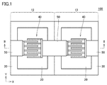
- FIG. 1 is a plan view of an elastic wave device 100 according to the first embodiment.
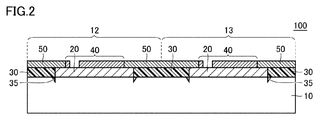
- FIG. 2 is a cross-sectional view taken along the line II-II of the elastic wave device 100 of FIG.
- the acoustic wave device 100 includes a support substrate 10 and resonating portions 12 and 13 formed adjacent to each other on the support substrate 10.
- the number of resonating units may be three or more.
- a case where a SAW filter is formed in the resonance unit will be described as an example, but the resonance unit may be formed of a BAW filter.
- the support substrate 10 is made of, for example, lithium tantalate (LiTaO 3 ), lithium niobate (LiNbO 3 ), a piezoelectric material such as quartz, alumina (Al 2 O 3 ), magnesia, silicon nitride (SiN), aluminum nitride (AlN). , Silicon carbide (SiC), zirconia (ZrO 2 ), cordierite, mullite, steatite, forsterite, and other ceramics; dielectrics such as glass; and semiconductors such as silicon (Si), sapphire, gallium nitride (GaN); A resin substrate or the like can be used.
- LiTaO 3 lithium tantalate
- LiNbO 3 lithium niobate
- a piezoelectric material such as quartz, alumina (Al 2 O 3 ), magnesia, silicon nitride (SiN), aluminum nitride (AlN).
- Each of the resonators 12 and 13 includes a piezoelectric thin film 20 and an elastic wave resonator formed of a comb-like electrode (IDT: Interdigital Transducer) 40 formed on the piezoelectric thin film 20.
- IDT Interdigital Transducer
- the piezoelectric thin film 20 and the IDT electrode 40 form a surface acoustic wave resonator (SAW filter).
- the piezoelectric thin film 20 is formed of, for example, a piezoelectric single crystal material such as lithium tantalate, lithium niobate, zinc oxide (ZnO), aluminum nitride, or lead zirconate titanate (PZT), or a piezoelectric laminated material thereof.
- the IDT electrode 40 is made of aluminum (Al), copper (Cu), silver (Ag), gold (Au), titanium (Ti), tungsten (W), platinum (Pt), chromium (Cr), nickel (Ni). ), Molybdenum (Mo), or a metal material such as an alloy containing these as a main component.
- the IDT electrode 40 may have a structure in which a plurality of metal films made of these metals or alloys are stacked.
- the periphery of the piezoelectric thin film 20 of the resonance parts 12 and 13 is surrounded by the support layer 30.
- the piezoelectric thin film 20 of the resonance unit 12 and the piezoelectric thin film 20 of the resonance unit 13 are divided by the support layer 30.
- the piezoelectric thin films 20 of the respective resonance parts 12 and 13 are arranged independently on the common support substrate 10.
- the support layer 30 is formed of a material having a smaller coefficient of linear expansion than the piezoelectric thin film 20, and for example, silicon dioxide (SiO 2 ) or polyimide (PI) is used.
- a wiring part 50 for electrically connecting the adjacent resonance parts 12, 13 is formed as necessary.
- reflectors may be arranged on both sides of the IDT electrode 40 on the piezoelectric thin film 20 (Y-axis direction in FIG. 1).
- the convex portion 35 is formed by filling the concave portion formed on the support substrate 10 with the material of the support layer 30 in the manufacturing process of the acoustic wave device 100.
- the protrusions 35 can suppress shrinkage that occurs when the polyimide is cured in the manufacturing process, and cracks occur between the piezoelectric thin film 20 and the support layer 30. Can be prevented.
- the piezoelectric thin films 20 of the adjacent resonance parts 12 and 13 are divided by the support layer 30 having a smaller linear expansion coefficient than the piezoelectric thin film 20. Therefore, even when a temperature difference occurs between the piezoelectric thin films 20 of the two resonance portions 12 and 13, the deformation of one of the piezoelectric thin films is prevented from affecting the other piezoelectric thin film by the surrounding support layer 30. be able to. Thereby, deterioration of the TCF characteristics can be suppressed.
- the piezoelectric thin film 20 of each resonance unit is directly arranged on the support substrate 10. However, if the piezoelectric thin film 20 is divided, the distance between the piezoelectric thin film 20 and the support substrate 10 can be reduced. May be provided with another layer.
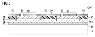
- FIG. 3 is a cross-sectional view of elastic wave device 100A according to the second embodiment.
- the elastic wave device 100A is different from the elastic wave device 100 of the first embodiment in that an intermediate layer 60 is provided between the piezoelectric thin film 20 and the support layer 30 and the support substrate 10.
- the protrusion 35 in the support layer 30 is located in the intermediate layer 60.
- the intermediate layer 60 includes at least the high sound velocity layer 62 that propagates an elastic bulk wave faster than the velocity of the elastic wave propagating to the piezoelectric thin film 20.
- the high sound velocity layer 62 include a DLC (Diamond-like Carbon) film, a piezoelectric material such as aluminum nitride, aluminum oxide, silicon carbide, silicon nitride, silicon, sapphire, lithium tantalate, lithium niobate, quartz, alumina, and zirconia.
- the high sound velocity layer 62 can effectively confine the energy of the elastic wave excited from the IDT electrode 40 to the piezoelectric thin film 20 in the piezoelectric thin film 20.
- the intermediate layer 60 includes, in addition to the high sonic layer 62, the low sonic layer 61, which is stacked on the high sonic layer 62 and propagates an elastic bulk wave lower in speed than the elastic wave propagating to the piezoelectric thin film 20. Further, the configuration may be provided.
- the low sound velocity layer 61 is made of, for example, silicon oxide, glass, silicon oxynitride, tantalum oxide, a compound obtained by adding fluorine, carbon, or boron to silicon oxide, or a material containing any of the above materials as a main component. Can be. 3 shows an example in which the intermediate layer 60 is formed as a laminate in which the low sound speed layers 61 and the high sound speed layers 62 are alternately stacked.
- the elastic wave is reflected at the interface between the low sound speed layer 61 and the high sound speed layer 62 or at the interface between the piezoelectric thin film 20 and the high sound speed layer 62, so that the acoustic wave is excited by the IDT electrode 40.
- the energy of the elastic wave can be effectively confined in the piezoelectric thin film 20 and the low sound speed layer 61.
- the thickness of the piezoelectric thin film 20 When the thickness of the piezoelectric thin film 20 is large, the influence of the material of the piezoelectric thin film 20 (for example, lithium tantalate) increases, so that elastic waves are not easily leaked in the thickness direction of the substrate. Is thicker, the effect of the linear expansion coefficient of the piezoelectric thin film 20 increases. Therefore, when the thickness of the piezoelectric thin film 20 increases, the TCF characteristics may deteriorate. Furthermore, since it becomes difficult to benefit from the support substrate 10 (for example, silicon) having high heat conductivity, TCF characteristics may be degraded.
- the support substrate 10 for example, silicon
- the thickness of the piezoelectric thin film 20 is preferably 3.5 ⁇ or less when the wavelength of the elastic wave determined from the electrode period of the IDT electrode 40 is ⁇ , and thus the Q value can be increased.
- the TCF characteristic can be improved by setting the thickness of the piezoelectric thin film 20 to 2.5 ⁇ or less, and the sound speed can be easily adjusted by setting the thickness to 1.5 ⁇ or less.
- the thickness of the low sound velocity layer 61 By setting the thickness of the low sound velocity layer 61 to 2.0 ⁇ or less, the film stress can be reduced, and the warpage of the substrate can be reduced. As a result, the yield rate of the acoustic wave device can be improved, and the characteristics can be stabilized.
- the high sound speed layer 62 is thin and the sound speed of the support substrate 10 is low, the surface acoustic waves are likely to leak to the support substrate 10. Then, the characteristics of the device may deteriorate due to the influence of the bulk radiation. As described above, since the function of confining the energy of the elastic wave in the piezoelectric thin film 20 and the low sound velocity layer 61 is exhibited by the high sound velocity layer 62, it is preferable that the thickness of the high sound velocity layer 62 be as large as possible.
- the intermediate layer 60 is provided with the high sonic layer.
- the support substrate 10 itself is formed of the high sonic layer material, and the intermediate layer 60 is formed of the low sonic layer material. Is also good.
- an intermediate layer 60 in which a high sound speed layer and a low sound speed layer are stacked may be provided between the support substrate 10 formed of the material of the high sound speed layer and the piezoelectric thin film 20.
- the intermediate layer 60 is composed of a high sonic layer and a low sonic layer determined by a relative velocity difference between the velocity of the elastic bulk wave propagating in each layer and the velocity of the elastic wave propagating in the piezoelectric thin film 20.
- a relative velocity difference between the velocity of the elastic bulk wave propagating in each layer and the velocity of the elastic wave propagating in the piezoelectric thin film 20 has been described, but another configuration can be adopted as a configuration for confining the energy of the elastic wave.
- the intermediate layer 60 may be configured such that layers having relatively different acoustic impedances are alternately stacked. That is, the portion of the low sound speed layer 61 in FIG. 3 is a low impedance layer (first layer) having a relatively low acoustic impedance, and the portion of the high sound speed layer 62 is a high impedance layer (the second layer) having a relatively high acoustic impedance. Layer). With such a configuration, since the elastic wave is reflected at the interface between the low impedance layer and the high impedance layer, the energy of the elastic wave excited by the IDT electrode 40 can be effectively confined in the piezoelectric thin film 20. Becomes possible.
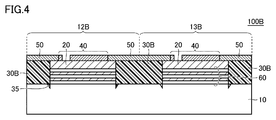
- FIG. 4 is a cross-sectional view of elastic wave device 100B according to the third embodiment.
- support layer 30B disposed around piezoelectric thin film 20 in each resonance portion extends to support substrate 10, and intermediate layer 60 is divided by support layer 30B. It is in a state. That is, in the intermediate layer 60, the portion between the piezoelectric thin film 20 of the first resonance section 12B and the support substrate 10 and the portion between the piezoelectric thin film 20 of the second resonance section 13B and the support substrate 10 are the first It is divided by a support layer 30B between the resonance part 12B and the second resonance part 13B.
- the protrusion 35 provided on the edge of the lower surface of the support layer 30 ⁇ / b> B is located in the support substrate 10.
- the configuration of the intermediate layer 60 is the same as that of the second embodiment, and may be a combination of a high sonic layer and a low sonic layer, or a combination of a high impedance layer and a low impedance layer. You may.
- the energy of the elastic wave excited by the IDT electrode 40 can be effectively confined in the piezoelectric thin film 20 by the intermediate layer 60.
- the position of the lower surface of the support layer 30B that divides the intermediate layer 60 does not necessarily have to coincide with the boundary between the support substrate 10 and the intermediate layer 60 as shown in FIG.
- the lower surface of the support layer 30C may be located closer to the intermediate layer 60 than the boundary between the support substrate 10 and the intermediate layer 60. In this case, the damage to the support substrate 10 can be reduced by preventing the protrusion 35 from being inside the support substrate 10.
- the lower surface of the support layer 30D may be positioned in the direction (first direction) closer to the support substrate 10 than the boundary between the support substrate 10 and the intermediate layer 60.
- the interface between the support substrate 10 and the high sound speed layer 62 It is known that a layer (charge generation layer 15) in which charges are generated is formed.
- the support layer 30E by adopting polyimide as the support layer 30E and arranging such that the lower surface thereof is closer to the support substrate 10 than the boundary between the support substrate 10 and the intermediate layer 60, the charge accumulated in the charge generation layer 15 is obtained. Can be effectively suppressed from moving to the adjacent resonance part.
- FIG. 8 is an example of a manufacturing process for forming the IDT electrode 40 before forming the support layer 30B
- FIG. 9 is an example of a manufacturing process for forming the IDT electrode 40 after forming the support layer 30B.
- a support substrate 10, an intermediate layer 60, and a piezoelectric thin film 20 are prepared, and the support substrate 10 and the piezoelectric thin film 20 are bonded together via the intermediate layer 60 to form an elastic wave device.
- a substrate having a basic structure is formed.
- the intermediate layer 60 is formed from the high sonic layer and the low sonic layer prior to the process of FIG. Process to be added.
- an IDT electrode 40 is formed on the surface of the piezoelectric thin film 20 on the substrate formed in FIG. 8A (FIG. 8B).
- other functional elements for example, capacitors, reflectors, etc.
- the functional element such as the IDT electrode 40 is formed on the piezoelectric thin film 20
- a portion where the piezoelectric thin film 20 and the intermediate layer 60 are left on the substrate surface is subjected to dry etching after masking, as shown in FIG.
- the portion of the piezoelectric thin film 20 and the intermediate layer 60 where the support layer 30B is to be formed is removed.
- the concave portion 75 is formed in the support substrate 10 by performing dry etching while covering the portion other than the portion where the concave portion 75 is to be formed with the resist.
- the position of the lower surface of the support layer is adjusted according to the degree of execution of the etching in FIG. 8C, as shown in FIGS.
- the support layer 30B is formed by filling the opening 70 formed by etching with, for example, polyimide.
- silicon dioxide (SiO 2 ) is used as the support layer 30B
- the support layer 30B is formed by a film forming process.
- the recess 75 formed in FIG. 8C is filled with the material of the support layer 30B to form the protrusion 35 of the support layer 30B (FIG. 8D).
- the opening 70 formed by removing the piezoelectric thin film 20 and the intermediate layer 60 is filled with a material for the support layer to form the support layer 30B (FIG. 9C). Then, a functional element such as the IDT electrode 40 is formed (FIG. 9D).
- the acoustic wave device 100B is formed by forming the wiring portion 50 on the support layer 30B (FIG. 9E).
- FIG. 10 is a cross-sectional view of an elastic wave device 100F formed in a WLP (Wafer Level Package) structure according to the fourth embodiment.
- WLP Wafer Level Package
- three resonating portions are formed on the supporting substrate 10, and the piezoelectric thin film 20 and the intermediate layer 60 of each resonating portion are divided by the supporting layer 30F.
- the support layer 30F of the elastic wave device 100F has a structure in which the height of the surface opposite to the support substrate 10 side is higher than the piezoelectric thin film 20, and the surface thereof partially overlaps the surface of the piezoelectric thin film 20. I have.
- a resin such as polyimide
- thermal contraction occurs due to a difference in linear expansion coefficient between the piezoelectric thin film 20 and the support layer 30F, the intermediate layer 60, and the piezoelectric layer.
- a gap may be generated between the thin film 20 and the thin film 20.
- by forming a structure in which a part of the support layer 30F overlaps the surface of the piezoelectric thin film 20 it is possible to prevent the generation of the void. As a result, disconnection of the wiring portion 50F formed on the upper surface of the support layer 30F can be prevented.
- a support member 80 for supporting the upper cover portion 90 is formed in the outermost support layer 30F in order to form the WLP structure.
- the support member 80 is made of a resin such as polyimide, and is arranged so as to surround the entirety of the plurality of resonance units provided therein.
- the cover 90 is made of, for example, a resin such as epoxy or a material such as insulating ceramic.
- the support member 80 and the cover 90 form an internal space in which the resonance unit including the ITD electrode 40 can vibrate. .
- a support member 82 for supporting the cover unit 90 is provided on the support layer 30F that divides the resonance unit.
- the support member 82 prevents the internal space from being crushed due to the deformation of the cover 90.
- the support member 80 and the cover portion 90 are formed with through-holes extending to the wiring portion 50F formed on the upper surface of the outermost support layer 30F, and the through-holes are filled with the under bump metal 95.
- the under bump metal 95 for example, a conductor such as Au, Ag, Cu, or Ni is used.
- a solder bump 96 is connected to the under bump metal 95, and the resonance unit and the external device are electrically connected via the under bump metal 95 and the solder bump 96.
- Such an elastic wave device 100F may be entirely molded with resin or the like after being mounted on an external substrate or the like. In such a case, pressure is applied to the cover 90 from the outside, so that the cover 90 is easily deformed. As described above, the deformation of the cover portion 90 is suppressed by providing the support member 82 on the support layer 30F that divides the resonance section. However, the thickness of the support layer 30F on which the support member 82 is provided (see FIG. 10). HB) is larger than the thickness of the outermost support layer 30F (HA in FIG. 10) (HA ⁇ HB), and the height of the cover 90 near the center of the elastic wave device 100F is changed to the cover of the outer periphery. By making the cover 90 higher than the height of the cover 90 (ie, making the cover 90 convex), the durability against external pressure can be further increased.
- the thickness of the support layer 30F on which the support member 82 is provided be thicker than the thickness of the outermost support layer 30F.
- the thickness may be set, or conversely, the thickness of the outermost support layer 30F may be increased.
- a part of the support layer 30F has a shape overlapping with the surface of the piezoelectric thin film 20 in order to prevent disconnection of the wiring part 50F, but by devising the shape of the wiring part, Further, the stress applied to the wiring portion can be reduced.
- a protrusion 55 is formed in the wiring portion 50G at a portion located at the boundary between the support layer 30G and the piezoelectric thin film 20.
- the shape of the protruding portion 55 is more preferably a curved shape as shown in FIG. 11 than a rectangular shape. With the curved shape, stress applied to the boundary between the support layer 30G and the piezoelectric thin film 20 and the portion where the protrusion 55 overlaps can be reduced.
- the shape of the wiring portion 50G shown in FIG. 11 can be applied to the first to third embodiments.
- the high impedance layer having a relatively high acoustic impedance and the low impedance layer having a relatively low acoustic impedance are alternately laminated as an intermediate layer for reflecting elastic waves, the high impedance layer is formed.
- tungsten (W), tantalum (Ta), niobium (Nb), or platinum (Pt) is used as a material.
- Tungsten, tantalum, niobium and platinum are materials that can cause migration due to moisture or outside air. When migration occurs, a part of the high-impedance layer is deficient and elastic waves cannot be appropriately reflected, and the characteristics of the elastic wave device may be changed.
- a description will be given of a configuration in which a protective layer is disposed on an elastic wave device to suppress migration of a high impedance layer in an intermediate layer.
- FIG. 12 is a cross-sectional view of elastic wave device 100H according to the fifth embodiment.
- FIGS. 12A to 12D show variations of the arrangement of the protective layer.
- the protective layer for example, a material such as silicon oxide or silicon nitride is used.
- the protective layer 76 covers the side surface of the laminated body of the support substrate 10, the intermediate layer 60 and the piezoelectric thin film 20, and the surface of the piezoelectric thin film 20 on which the IDT electrode 40 is formed. It is formed as follows. Such a configuration is realized by laminating the protective layer 76 before the step of forming the support layer 30B (between FIG. 8C and FIG. 8D) in the manufacturing process described with reference to FIG. Is done.
- the support layer 30 and the intermediate layer 60 are separated from each other by the protective layer 76, and the surface of the piezoelectric thin film 20 is shielded from the outside air. Therefore, the protection layer 76 can prevent moisture or the like that has passed through the support layer 30 or the piezoelectric thin film 20 from reaching the high impedance layer 62. This can suppress the occurrence of migration in the material forming the high impedance layer 62.
- a protective layer 76 is formed so as to cover the surfaces of the support layer 30 and the piezoelectric thin film 20. Then, the wiring portion 50 is formed on the upper surface of the protective layer 76 (the surface of the protective layer 76 opposite to the side of the piezoelectric thin film 20). The wiring section 50 is connected to the IDT electrode 40 arranged on the piezoelectric thin film 20 by an opening formed in the protective layer 76.
- Such a configuration is realized by laminating the protective layer 76 after the step of FIG. 8D or FIG. 9D.
- the support layer 30 and the piezoelectric thin film 20 are prevented from being exposed to the outside air, and the permeation of moisture into the support layer 30 and the piezoelectric thin film 20 can be prevented. Therefore, it is possible to suppress migration from occurring in the material forming the high impedance layer 62.
- the wiring portion 50 is also covered by the protective layer.
- Such a configuration is realized by laminating the protective layer 76 after the step of FIG. 8E or FIG. 9E.
- the wiring portion 50 is also covered by the protective layer 76. Therefore, like the elastic wave devices 100H1 and 100H2, an opening is formed in the protective layer 76 to allow the wiring portion 50 to pass therethrough. No need to form. Therefore, it is possible to further suppress the moisture from reaching the high impedance layer 62 through the opening. This can suppress the occurrence of migration in the material forming the high impedance layer 62.
- the protective layer 77 is formed only at the boundary between the high impedance layer 62 (second layer) and the support layer 30 in the intermediate layer 60.
- the protective layer 77 may be formed by forming a material such as silicon oxide or silicon nitride on the end of the high impedance layer 62 as in the first to third examples described above.
- the tungsten may be formed by oxidizing or nitriding an end portion of the tungsten.
- Embodiment 6 In each of the above embodiments, the configuration of the acoustic wave device in which a pair of adjacent resonance units are connected by the wiring unit has been described.
- FIG. 13 shows an elastic wave device 100J1 according to the sixth embodiment.
- the upper part (FIG. 13A) shows a plan view of the acoustic wave device 100J1
- the lower part shows a cross-sectional view taken along the XIII-XIII plane in the plan view. It is shown.
- elastic wave device 100J1 includes four IDT electrodes 41 to 44 arranged on piezoelectric thin film 20, and a resonance section is formed for each IDT electrode.
- the piezoelectric thin film 20 is disposed on the support substrate 10 with the intermediate layer 60 interposed therebetween, and the IDT electrode is formed on the piezoelectric thin film 20.
- the four resonance units are adjacent to each other via the common support layer 30G. More specifically, IDT electrode 41 and IDT electrode 42 are adjacent to each other in the X-axis direction via support layer 30G, and IDT electrode 43 and IDT electrode 44 are in the Y-axis direction via support layer 30G. Is adjacent to
- the wiring portions for connecting the IDT electrodes are mutually connected. Will cross. In this case, if the two wiring portions are arranged on the same plane, the wiring portions are short-circuited, so that it is necessary to largely bypass one of the wiring portions. Then, the area of the entire elastic wave device increases, which may be a factor that hinders downsizing of devices formed by the elastic wave device.
- the two wiring portions when two wiring portions intersect, the two wiring portions are formed in different layers in the intersection region and are arranged three-dimensionally, so that the size of the elastic wave device is increased. Insulation between the wiring parts is ensured while suppressing.
- the metal layer 85 is formed inside the support layer 30G, and the wiring portions 51 and 52 formed on the surface of the support layer 30G.
- the IDT electrode 41 and the IDT electrode 42 are connected by the and the metal layer 85.
- the IDT electrode 43 and the IDT electrode 44 are connected by a wiring portion 53 formed in a region between the wiring portion 51 and the wiring portion 52 on the surface of the support layer 30G. That is, in a region where the path connecting the IDT electrode 41 and the IDT electrode 42 and the path connecting the IDT electrode 43 and the IDT electrode 44 intersect when the elastic wave device 100J1 is viewed in plan, the support layer 30G is formed. Insulated by the insulating material to be formed.
- FIG. 13 illustrates an example in which two wires connecting the IDT electrodes intersect
- the above configuration is not limited to the wires connecting the IDT electrodes, and two wires in the acoustic wave device are provided.
- the present invention can be applied to other portions where wirings intersect.
- the wiring extending from the IDT electrode to the terminal at the end of the circuit may intersect with another wiring, or the wiring extending from one IDT electrode may intersect.
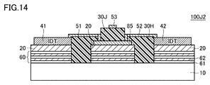
- FIG. 14 is a cross-sectional view of an elastic wave device 100J2 according to a modification of the sixth embodiment.
- the metal layer 85 is formed inside the support layer 30G.
- the metal layer 85 is formed on the intermediate layer 60 similarly to the resonance part.
- a metal layer 85 is formed on the piezoelectric thin film 20 thus formed.
- a support layer 30H is disposed around the intermediate layer 60 on which the metal layer 85 is formed, and the IDT electrodes are adjacent to each other via the support layer 30H.
- the IDT electrode 41 and the IDT electrode 42 are connected by wiring portions 51 and 52 formed on the surface of the support layer 30H and the metal layer 85, similarly to the elastic wave device 100J1.
- a support layer 30J is disposed above the metal layer 85, and a wiring portion 53 for connecting the IDT electrode 43 and the IDT electrode 44 is formed on the surface of the support layer 30J.
- the intersection region of the wiring portions can be arranged three-dimensionally, so that the insulation between the wiring portions can be suppressed while suppressing the size of the elastic wave device from increasing. Can be secured.
- an intersection region including the metal layer 85 can be simultaneously formed in the manufacturing process of the resonance section. Thereby, an additional step for forming the intersection region can be reduced.
- Embodiment 7 In some cases, a metal film is used as the high impedance layer of the intermediate layer. At this time, if the metal film is arranged to face the wiring portion, a capacitor is formed between the wiring portion and the metal film. In the case of an SMR (Solidly Mounted Resonator) type resonator in which high impedance layers and low impedance layers are alternately arranged, a metal film is formed at a position facing the IDT electrode in order to reflect an elastic wave in the intermediate layer. You. Therefore, when the metal layer disposed to face the wiring portion and the metal layer disposed to face the IDT electrode are electrically connected, a state in which a capacitor is connected in parallel to the SAW resonator can be obtained. .
- SMR Solidly Mounted Resonator
- the elastic wave device is a ladder-type filter having a series arm circuit and a parallel arm circuit
- filter characteristics may be affected depending on a resonator to which a capacitor is connected in parallel.
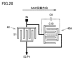
- FIG. 15 is a circuit diagram showing an example of a ladder-type filter 200 (hereinafter, also simply referred to as “filter 200”) according to the seventh embodiment.
- FIG. 16 is a schematic plan view of the elastic wave device (filter) shown in FIG.
- filter 200 includes a series arm circuit 201 connected between input terminal IN and output terminal OUT, and a parallel arm connected between series arm circuit 201 and ground potential. And a circuit 202.
- the series arm circuit 201 includes series arm resonators S1 to S3 connected in series between the input terminal IN and the output terminal OUT.
- the parallel arm circuit 202 includes parallel arm resonators P1 and P2.
- the parallel arm resonator P1 is connected between a connection node between the series arm resonators S1 and S2 and a ground potential.
- the parallel arm resonator P2 is connected between a connection node between the series arm resonators S2 and S3 and a ground potential.
- the configuration of the series arm circuit 201 and the parallel arm circuit 202 in the filter 200 is not limited to the configuration shown in FIG. 15, but may be another configuration.
- the series arm resonator and the parallel arm resonator correspond to the resonance unit in the above-described embodiment.
- the resonance frequency Frs of the series arm resonator and the anti-resonance frequency Fap of the parallel arm resonator are set near the center frequency of the target pass band, so that the parallel arm resonator A bandpass filter having a pass band between a resonance frequency Frp and an anti-resonance frequency Fap of the series arm resonator is formed.
- the specific band (Fa ⁇ Fr) / Fr).
- steepness of the attenuation characteristic between the pass band and the attenuation band may be required in order to increase the S / N ratio. It is generally known that reducing the bandwidth is effective for improving the steepness.
- the attenuation pole on the higher side of the pass band is determined by the series arm resonator. Therefore, in order to achieve a wider pass band and sharper attenuation characteristics on the high frequency side, it is effective to reduce the fractional band for the series arm resonator and increase the fractional band for the parallel arm resonator. It becomes.
- each resonator when the metal film 65 is provided on the high-impedance layer 62 of the intermediate layer 60, a capacitor is connected in parallel to the resonator (for example, C1, C2 in FIG. 15).
- the anti-resonance frequency moves to a lower frequency side, so that the fractional band generally becomes smaller. Therefore, it is preferable to reduce the influence of the metal film for the parallel arm resonator for which it is desired to increase the bandwidth.
- FIG. 17 is a cross-sectional view of a portion of region RG1 including series arm resonator S2 and parallel arm resonator P1 of FIG. 16 in elastic wave device 100K according to the seventh embodiment.
- elastic wave device 100K has a configuration in which piezoelectric thin film 20 and support layer 30 are formed on intermediate layer 60 as shown in FIG. 62 includes a metal film 65.
- the position where the metal film 65 is included in the intermediate layer 60 is not limited to the uppermost high impedance layer 62.
- the metal film 65 may be arranged at any one of the layers constituting the intermediate layer 60 or at the interface between two adjacent layers.
- the left resonating part corresponds to the series arm resonator S2, and the right resonating part corresponds to the parallel arm resonator P1.
- the metal film 65 is formed over the piezoelectric thin film 20 and the support layer 30 in the intermediate layer 60A.
- the parallel arm resonator P ⁇ b> 1 the metal film 65 is formed in a portion facing the IDT electrode 40, but the metal film 65 is not formed in a portion facing the wiring portion 50. That is, when the elastic wave device 100K is viewed in a plan view, the wiring portion 50 and the metal film 65 do not overlap in the parallel arm resonator P1.
- the support layer 30 extends from the wiring portion 50 to the support substrate 10 without providing the intermediate layer 60A between the wiring portion 50 of the parallel arm resonator P1 and the support substrate 10. There may be.
- the metal film 65 is not formed on all the portions facing the wiring portion 50.
- the metal film 65 is formed on a portion of the parallel arm resonator P ⁇ b> 1 facing the wiring portion 50. Is also good.
- the wiring portion 50 and the metal film 65 face each other via the support layer 30 made of an insulating material, and a capacitor is formed in this portion. Then, a path (arrow AR1 in FIG. 17) from the input side IDT electrode of the series arm resonator S2 to the output side IDT electrode through the metal film 65 is formed, and the IDT electrode 40 of the series arm resonator S2 is formed.
- the configuration is such that the capacitors are connected in parallel.
- the wiring section 50 is not formed in the portion (region RG3) facing the wiring section 50, the wiring section 50 such as the series arm resonator S2 and the wiring section 50 are not formed. Does not occur. Therefore, a capacitor connected in parallel to the IDT electrode 40 of the parallel arm resonator P1 is not formed.
- the elastic wave device of the ladder type filter in which the metal film is used as the high impedance layer of the intermediate layer when the elastic wave device is viewed in a plan view, the wiring portion connected to the parallel arm resonator and the metal film are separated. By adopting a configuration that does not overlap, the influence on the filter characteristics can be reduced.
- Embodiment 8 As described in the seventh embodiment, in the ladder-type filter, by connecting a capacitor in parallel with the series arm resonator to reduce the fractional band of the series arm resonator, the bandwidth of the band-pass filter is increased. The steepness of the attenuation characteristic on the side can be increased.
- FIG. 18 is a circuit diagram showing an example of ladder-type filter 200A according to the eighth embodiment.
- the filter 200A has a configuration in which a bridging capacitor C10 is connected in parallel to the series arm resonator S1 in addition to the configuration of the filter 200 of the seventh embodiment.
- the bridge capacitance section C10 of the filter 200A has the same configuration as each resonator (resonance section) included in the series arm circuit 201 and the parallel arm circuit 202.
- the bridging capacitor C10 has a configuration in which the IDT electrode 40A is formed on the piezoelectric thin film 20 laminated on the intermediate layer 60A.
- the electrode fingers of the IDT electrode 40A of the bridging capacitance portion C10 are arranged so as to be parallel to the propagation direction of the surface acoustic wave. I have. Therefore, the IDT electrode 40A does not excite with a surface acoustic wave and functions as a capacitor.
- the metal film 65 is disposed on the uppermost high impedance layer 62 of the intermediate layer 60A of the bridging capacitor C10 so as to face the piezoelectric thin film 20 and the support layer 30.
- the configuration is such that the capacitor C0 is connected in parallel to the IDT electrode 40A forming the bridging capacitance portion C10.
- the capacitance of the bridging capacitance portion C10 can be reduced by using the capacitor C0 formed by the metal film 65 of the intermediate layer 60A. Since the capacitance of the bridging capacitor C10 is determined by the size of the IDT electrode 40A, the size of the bridging capacitor C10 can be reduced as a result.
- FIG. 18 illustrates an example of a configuration in which the bridging capacitance portion is disposed with respect to the series arm resonator S1, instead of or in addition to this, the series arm resonator S2 and / or the series arm resonator may be arranged.
- a bridging capacitance section may be provided in S3.
- Embodiment 9 As described in the seventh and eighth embodiments, in the configuration in which the metal film is provided on the high impedance layer of the intermediate layer in the ladder-type filter, the wiring portion and the metal film are opposed to each other so as to be connected to the resonator in parallel. Capacitor can be formed.
- the fractional band of the series arm resonator can be adjusted. Therefore, in the ninth embodiment, a configuration in which the capacitance of the capacitor connected in parallel for each series arm resonator can be adjusted by adjusting the area where the wiring portion and the metal film overlap each other for each series arm resonator. explain.
- FIG. 21 is a schematic plan view of a ladder-type filter 200B according to the ninth embodiment.
- the filter 200B has a circuit basically similar to the circuit diagram shown in FIG. 15 of the seventh embodiment, and is configured by series arm resonators S1 to S3 and parallel arm resonators P1 and P2. I have.
- FIG. 22 is a plan view of an elastic wave device 100L corresponding to the series arm resonators S1 and S2 in the filter 200B.
- the metal film 65 is disposed on the high impedance layer of the intermediate layer so as to face the wiring portions on the input side and the output side of each series arm resonator (FIG. 22).
- the capacitor C11 is formed between the input side wiring portion 56 and the output side wiring portion 57.
- a capacitor C12 is formed between the input side wiring portion 57 and the output side wiring portion 58.
- a capacitor C13 is formed between the input side wiring portion 58 and the output side wiring portion 59.
- the capacitance of the capacitor formed by each wiring portion and the metal film 65 can be adjusted by changing the area where the metal film 65 overlaps the input-side and output-side wiring portions forming the capacitor.
- the capacitance of the capacitor can be changed by adjusting the line width of each wiring portion.
- the line width of the wiring portion may be fixed, and the width of the metal film 65 facing each wiring portion may be individually changed.
- the input-side wiring portion indicates a wiring portion connected to the input-side bus bar of the IDT electrode in each resonator, and the output-side wiring portion corresponds to the output-side bus bar of the IDT electrode in each resonator. The wiring part to be connected is shown.
- the fractional band can be adjusted for each series arm resonator. Therefore, the degree of freedom in designing a ladder-type filter can be increased.
Landscapes
- Physics & Mathematics (AREA)
- Acoustics & Sound (AREA)
- Engineering & Computer Science (AREA)
- Manufacturing & Machinery (AREA)
- Surface Acoustic Wave Elements And Circuit Networks Thereof (AREA)
Abstract
弾性波装置(100)は、支持基板(10)と、当該支持基板(10)上に隣接して形成された共振部(12,13)とを備える。共振部(12,13)の各々は、圧電薄膜(20)と、圧電薄膜(20)上に配置されたIDT電極(40)と、弾性波装置(100)を平面視した場合に圧電薄膜(20)の周囲を囲むように配置された支持層(30)とを含む。支持層(30)は、圧電薄膜(20)とは異なる線膨張係数を有する。共振部(12)の圧電薄膜と、共振部(13)の圧電薄膜とは、共振部(12)と共振部(13)との間にある支持層(30)によって分割されている。このような構成により、共通の支持基板上に複数の弾性波共振子が形成された弾性波装置におけるTCF特性を向上することができる。
Description
本開示は弾性波装置に関し、より特定的には、弾性波装置の温度特性を改善するための技術に関する。
近年、携帯電話あるいはスマートフォンなどの通信機器においては、複数の周波数帯域の電波を用いて通信を行なうマルチバンド通信が進められている。これに伴い、このような通信機器においては、受信した電波を各周波数帯域の信号に分割するために、複数のフィルタを有するマルチプレクサが一般的に用いられる。
マルチプレクサに用いられるフィルタとして、たとえば弾性表面波(Surface Acoustic Wave:SAW)フィルタあるいはバルク弾性波(Bulk Acoustic Wave:BAW)フィルタなどを用いることができる。携帯端末においては、機器の小型化のために、これらのフィルタを同一基板上に形成したワンチップ構造のマルチプレクサが採用される場合がある。
特開2018-7239号公報(特許文献1)には、同一の支持基板内において、複数の弾性波共振子が形成された弾性波装置が開示されている。特開2018-7239号公報(特許文献1)の弾性波装置においては、共通の圧電薄膜上に複数の弾性波共振子が形成され、当該圧電薄膜の外周に別材料で形成された支持層が配置されている。
圧電薄膜上に弾性波共振子が形成された弾性波装置においては、弾性波共振子に電流が流れると、それに伴って弾性波共振子および圧電薄膜の温度が上昇する。特開2018-7239号公報(特許文献1)の弾性波装置のように、複数の弾性波共振子が形成される場合、使用する周波数帯域の偏りなどによって各弾性波共振子の使用頻度が異なると、共通の圧電薄膜に温度分布が生じて圧電薄膜が局部的に変形し、これにより周波数温度係数(Temperature Coefficients of Frequency:TCF)特性が悪化する可能性がある。
本開示は、このような課題を解決するためになされたものであって、その目的は、共通の支持基板上に複数の弾性波共振子が形成された弾性波装置におけるTCF特性を向上させることである。
本開示に従う弾性波装置は、支持基板と、当該支持基板上に隣接して形成された第1共振部および第2共振部とを備える。第1共振部および第2共振部の各々は、圧電薄膜と、圧電薄膜上に配置されたIDT電極と、弾性波装置を平面視した場合に圧電薄膜の周囲を囲むように配置された支持層とを含む。支持層は、圧電薄膜とは異なる線膨張係数を有する。第1共振部の圧電薄膜と、第2共振部の圧電薄膜とは、第1共振部と第2共振部との間にある支持層によって分割されている。
本開示による弾性波装置においては、圧電薄膜が共振部毎に分割され、圧電薄膜とは異なる線膨張係数を有する支持層によって各圧電薄膜の周囲が囲まれる構成となっている。これにより、圧電薄膜の温度が上昇しても、線膨張係数の異なる支持層によって圧電薄膜の変形が抑制され、隣接する共振部への影響も抑制できる。したがって、弾性波装置のTCF特性を改善することができる。
以下、本開示の実施の形態について、図面を参照しながら詳細に説明する。なお、図中同一または相当部分には同一符号を付してその説明は繰り返さない。
[実施の形態1]
図1は、実施の形態1に従う弾性波装置100の平面図である。また、図2は、図1の弾性波装置100のII-II面における断面図である。
図1は、実施の形態1に従う弾性波装置100の平面図である。また、図2は、図1の弾性波装置100のII-II面における断面図である。
図1および図2を参照して、弾性波装置100は、支持基板10と、当該支持基板10上に互いに隣接して形成された共振部12,13とを備える。なお、実施の形態1においては、弾性波装置に2つの共振部が備えられる場合を例として説明するが、共振部は3つ以上であってもよい。また、以降の説明においては、共振部にSAWフィルタが形成される場合を例として説明するが、共振部がBAWフィルタで形成されていてもよい。
支持基板10は、たとえば、タンタル酸リチウム(LiTaO3)、ニオブ酸リチウム(LiNbO3)、水晶等の圧電体、アルミナ(Al2O3)、マグネシア、窒化ケイ素(SiN)、窒化アルミニウム(AlN)、炭化ケイ素(SiC)、ジルコニア(ZrO2)、コージライト、ムライト、ステアタイト、フォルステライト等の各種セラミック、ガラス等の誘電体またはシリコン(Si)、サファイア、窒化ガリウム(GaN)等の半導体及び樹脂基板等を用いることができる。
共振部12,13の各々は、圧電薄膜20と、圧電薄膜20上に形成された櫛歯状電極(IDT:Interdigital Transducer)40からなる弾性波共振子とを含む。圧電薄膜20とIDT電極40とによって弾性表面波共振子(SAWフィルタ)が形成される。
圧電薄膜20は、たとえば、タンタル酸リチウム、ニオブ酸リチウム、酸化亜鉛(ZnO)、窒化アルミニウム、またはチタン酸ジルコン酸鉛(PZT)などの圧電単結晶材料、あるいはそれらの圧電積層材料によって形成される。また、IDT電極40は、アルミニウム(Al)、銅(Cu)、銀(Ag)、金(Au)、チタン(Ti)、タングステン(W)、白金(Pt)、クロム(Cr)、ニッケル(Ni)、モリブデン(Mo)のうちの少なくとも一種からなる単体金属、またはこれらを主成分とする合金などの金属材料を用いて形成することができる。また、IDT電極40は、これらの金属もしくは合金からなる複数の金属膜を積層した構造を有していてもよい。
図1の平面図に示されるように、弾性波装置100を平面視した場合に、共振部12,13の圧電薄膜20の周囲は支持層30で囲まれている。図2の断面図に示されるように、共振部12の圧電薄膜20と共振部13の圧電薄膜20は、支持層30によって分割されている。言い換えると、各共振部12,13の圧電薄膜20は、共通の支持基板10上に互いに独立して配置されている。
支持層30は、圧電薄膜20よりも小さい線膨張係数を有する材料で形成されており、たとえば二酸化ケイ素(SiO2)あるいはポリイミド(PI)などが用いられる。支持層30の表面には、必要に応じて、隣接する共振部12,13を電気的に接続するための配線部50が形成される。なお、図には示されていないが、圧電薄膜20上のIDT電極40の両側(図1のY軸方向)に、反射器が配置されていてもよい。
また、図2の断面図に示されるように、支持層30の支持基板10側の面(下面)の縁部には、共振部12,13から支持基板10に向かう方向に突出した凸部35が形成されている。この凸部35は、図8および図9で後述するように、弾性波装置100の製造プロセスにおいて支持基板10に形成される凹部に支持層30の材料が充填されて形成されたものである。このような凸部35を設けることによって、支持層30が支持基板10に固定されて熱負荷の変動による支持層30の収縮が抑制されるため、支持層30と圧電薄膜20との間の熱応力を低減することができる。また、支持層30としてポリイミドを用いる場合、当該凸部35によって、製造過程においてポリイミドが硬化する際に生じる収縮を抑制することができ、圧電薄膜20と支持層30との間にクラックが発生することを防止できる。
本実施の形態1においては、図2に示されるように、隣接する共振部12,13の圧電薄膜20が、圧電薄膜20より小さい線膨張係数を有する支持層30によって分割されている。そのため、2つの共振部12,13の圧電薄膜20に温度差が生じた場合であっても、周囲を囲む支持層30によって一方の圧電薄膜の変形が他方の圧電薄膜に影響することを抑制することができる。これによって、TCF特性の悪化を抑制することができる。
[実施の形態2]
実施の形態1においては、支持基板10上に各共振部の圧電薄膜20が直接配置される構成であったが、圧電薄膜20が分割されていれば、圧電薄膜20と支持基板10との間に他の層が設けられていてもよい。
実施の形態1においては、支持基板10上に各共振部の圧電薄膜20が直接配置される構成であったが、圧電薄膜20が分割されていれば、圧電薄膜20と支持基板10との間に他の層が設けられていてもよい。
図3は、実施の形態2に従う弾性波装置100Aの断面図である。弾性波装置100Aにおいては、圧電薄膜20および支持層30と支持基板10との間に中間層60が設けられている点が、実施の形態1の弾性波装置100と異なっている。なお、支持層30における凸部35は、中間層60内に位置している。
中間層60は、圧電薄膜20に伝搬する弾性波の速度よりも高速の弾性バルク波を伝搬する高音速層62を少なくとも含む。高音速層62としては、たとえばDLC(Diamond-like Carbon)膜、窒化アルミニウム、酸化アルミニウム、炭化ケイ素、窒化ケイ素、シリコン、サファイア、タンタル酸リチウム、ニオブ酸リチウム、水晶等の圧電体、アルミナ、ジルコニア、コージライト、ムライト、ステアタイト、フォルステライト等の各種セラミック、マグネシアダイヤモンド、または、上記各材料を主成分とする材料、上記各材料の混合物を主成分とする材料のいずれかを用いることができる。この高音速層62によって、IDT電極40から圧電薄膜20に励振された弾性波のエネルギーを圧電薄膜20内に効果的に閉じ込めることができる。
なお、中間層60は、高音速層62に加えて、高音速層62上に積層された、圧電薄膜20に伝搬する弾性波の速度よりも低速の弾性バルク波を伝搬する低音速層61をさらに備える構成であってもよい。低音速層61は、たとえば、酸化ケイ素、ガラス、酸窒化ケイ素、酸化タンタル、酸化ケイ素にフッ素または炭素またはホウ素を加えた化合物、または、上記各材料を主成分とする材料のいずれかを用いることができる。図3の中間層60においては、低音速層61と高音速層62とが交互に積層された積層体として形成された例が示されている。
このような構成とすることによって、低音速層61と高音速層62との界面、あるいは圧電薄膜20と高音速層62との界面において弾性波が反射されるので、IDT電極40によって励振された弾性波のエネルギーを圧電薄膜20および低音速層61内に効果的に閉じ込めることが可能となる。
圧電薄膜20の厚みが厚いと、圧電薄膜20の材料(たとえば、タンタル酸リチウム)の影響の割合が大きくなることで、基板の厚さ方向に弾性波が漏洩しやすくない、また、圧電薄膜20の厚みが厚くなると、圧電薄膜20の線膨張係数の影響が大きくなる。そのため、圧電薄膜20の厚みが厚くなるとTCF特性が悪化し得る。さらに、伝熱性の高い支持基板10(たとえば、シリコン)の恩恵を受けにくくなるため、TCF特性が劣化し得る。
圧電薄膜20の厚みは、IDT電極40の電極周期から定まる弾性波の波長をλとしたときには3.5λ以下であることが好ましく、このようにすることでQ値を高くすることができる。また、圧電薄膜20の厚みを2.5λ以下とすることによってTCF特性を良くすることができ、さらに1.5λ以下とすることで音速の調整が容易になる。
低音速層61の厚みについては、2.0λ以下とすることによって膜応力を低減することができ、これにより基板の反りを低減することができる。その結果、弾性波装置の良品率が向上するとともに特性の安定化を実現できる。
高音速層62の厚みが薄く、支持基板10の音速が遅い場合には、弾性表面波が支持基板10に漏洩しやすくなる。そうすると、このバルク放射の影響によってデバイスの特性が劣化する場合が生じ得る。上述のように高音速層62によって弾性波のエネルギーを圧電薄膜20および低音速層61内に閉じ込める機能が発揮されるため、高音速層62の厚みはできるだけ厚くすることが好ましい。
なお、図3の構成においては、中間層60に高音速層を設ける構成としたが、支持基板10自体を高音速層の材料で形成し、中間層60を低音速層の材料で形成してもよい。あるいは、高音速層の材料で形成された支持基板10と圧電薄膜20との間に高音速層と低音速層とを積層した中間層60を設ける構成としてもよい。
(変形例)
上記の実施の形態2においては、中間層60は、各層に伝搬する弾性バルク波の速度と圧電薄膜20に伝搬する弾性波の速度との相対的な速度差によって定まる高音速層と低音速層とによって構成される例について説明したが、弾性波のエネルギーを閉じ込める構成として他の構成を採用することも可能である。
上記の実施の形態2においては、中間層60は、各層に伝搬する弾性バルク波の速度と圧電薄膜20に伝搬する弾性波の速度との相対的な速度差によって定まる高音速層と低音速層とによって構成される例について説明したが、弾性波のエネルギーを閉じ込める構成として他の構成を採用することも可能である。
変形例においては、中間層60として、相対的に音響インピーダンスの異なる層を交互に積層した構成とすることもできる。すなわち、図3における低音速層61の部分が相対的に音響インピーダンスが低い低インピーダンス層(第1層)とされ、高音速層62の部分が相対的に音響インピーダンスが高い高インピーダンス層(第2層)とされる。このような構成とすることで、低インピーダンス層と高インピーダンス層との界面で弾性波が反射されるので、IDT電極40によって励振された弾性波のエネルギーを圧電薄膜20内に効果的に閉じ込めることが可能となる。
[実施の形態3]
実施の形態2においては、共通の中間層60上に2つの共振部12,13が配置される構成について説明したが、中間層60は、必ずしも複数の共振部に対して共通に設けられる構成でなくてもよい。
実施の形態2においては、共通の中間層60上に2つの共振部12,13が配置される構成について説明したが、中間層60は、必ずしも複数の共振部に対して共通に設けられる構成でなくてもよい。
実施の形態3においては、圧電薄膜と同様に、中間層についても支持層によって分割される構成について説明する。
図4は、実施の形態3に従う弾性波装置100Bの断面図である。図4を参照して、弾性波装置100Bにおいては、各共振部において圧電薄膜20の周囲に配置された支持層30Bが支持基板10まで延在し、支持層30Bによって中間層60が分割された状態となっている。すなわち、中間層60における、第1共振部12Bの圧電薄膜20と支持基板10との間の部分と、第2共振部13Bの圧電薄膜20と支持基板10との間の部分とは、第1共振部12Bと第2共振部13Bとの間にある支持層30Bによって分割されている。このとき、支持層30Bの下面の縁部に設けられた凸部35は、支持基板10内に位置している。なお、中間層60の構成については、実施の形態2と同様であり、高音速層と低音速層との組み合わせであってもよいし、あるいは、高インピーダンス層と低インピーダンス層との組み合わせてあってもよい。
このように、中間層60が各共振部ごとに分割された構成においても、中間層60によって、IDT電極40によって励振された弾性波のエネルギーを圧電薄膜20内に効果的に閉じ込めることができる。
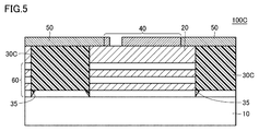
なお、中間層60を分割する支持層30Bの下面の位置については、必ずしも図4のように支持基板10と中間層60との境界と一致していなくてもよい。たとえば、図5の弾性波装置100Cのように、支持層30Cの下面が支持基板10と中間層60との境界よりも中間層60側に位置するようにしてもよい。この場合、凸部35が支持基板10内とならないようにすることで、支持基板10へのダメージを低減することができる。
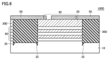
あるいは、図6の弾性波装置100Dのように、支持層30Dの下面が支持基板10と中間層60との境界よりも支持基板10側の方向(第1方向)に位置するようにしてもよい。特に、図7の弾性波装置100Eのように、支持基板10としてシリコンを採用し、低音速層61として二酸化ケイ素を採用するような場合には、支持基板10と高音速層62との界面に電荷が生じる層(電荷発生層15)が形成されることが知られている。この場合に、支持層30Eとしてポリイミドを採用し、その下面が支持基板10と中間層60との境界よりも支持基板10側となるように配置することで、電荷発生層15に蓄積された電荷が隣接する共振部に移動することを効果的に抑制することができる。
(弾性波装置の製造プロセス)
次に、図8および図9を用いて、図4で示した弾性波装置100Bの製造プロセスについて説明する。図8は、支持層30Bを形成する前にIDT電極40を形成する製造プロセスの例であり、図9は、支持層30Bを形成後にIDT電極40を形成する製造プロセスの例である。
次に、図8および図9を用いて、図4で示した弾性波装置100Bの製造プロセスについて説明する。図8は、支持層30Bを形成する前にIDT電極40を形成する製造プロセスの例であり、図9は、支持層30Bを形成後にIDT電極40を形成する製造プロセスの例である。
(第1プロセス例)
図8(a)を参照して、まず支持基板10、中間層60、および圧電薄膜20を準備し、中間層60を介して支持基板10と圧電薄膜20とを貼りあわせて、弾性波装置の基本構造となる基板を形成する。このとき、中間層60として高音速層と低音速層との積層体が用いられる場合には、図8(a)のプロセスに先立って、高音速層と低音速層とから中間層60を形成するプロセスが追加される。
図8(a)を参照して、まず支持基板10、中間層60、および圧電薄膜20を準備し、中間層60を介して支持基板10と圧電薄膜20とを貼りあわせて、弾性波装置の基本構造となる基板を形成する。このとき、中間層60として高音速層と低音速層との積層体が用いられる場合には、図8(a)のプロセスに先立って、高音速層と低音速層とから中間層60を形成するプロセスが追加される。
次に、図8(a)で形成された基板における圧電薄膜20の表面に、IDT電極40を形成する(図8(b))。なお、IDT電極40以外の他の機能素子(たとえばキャパシタ,反射器など)が圧電薄膜20上に設けられる場合には、この図8(b)の工程において形成される。
圧電薄膜20上にIDT電極40などの機能素子が形成されると、基板表面において圧電薄膜20および中間層60を残す部分にマスクを施した上でドライエッチングを行ない、図8(c)のように、支持層30Bを形成する部分の圧電薄膜20および中間層60を除去する。これによって形成された開口部70と中間層60との境界部分については、凹部75を形成する部分以外をレジストで覆った状態でドライエッチングすることで支持基板10に凹部75が形成される。なお、図8(c)におけるエッチングの実行度合いによって、図3~図7のように、支持層の下面の位置が調整される。
その後、図8(d)のように、エッチングにより形成された開口部70に、たとえばポリイミドを充填することによって支持層30Bを形成する。なお、支持層30Bとして二酸化ケイ素(SiO2)が用いられる場合には、支持層30Bは成膜処理によって形成される。このとき、図8(c)で形成された凹部75に支持層30Bの材料が充填されて、支持層30Bの凸部35が形成される(図8(d))。
その後、基板表面のマスクが除去され、支持層30B上に配線部50を形成することによって弾性波装置100Bが形成される(図8(e))。
(第2プロセス例)
図9の製造プロセスの例では、図9(a)において支持基板10、中間層60および圧電薄膜20を貼りあわせて基板が形成されると、IDT電極40などの機能素子を形成する部分にマスクを施してドライエッチングを行ない、支持層30Bが形成される部分の圧電薄膜20および中間層60を除去する(図9(b))。このとき、図8で説明したように、ドライエッチングの度合いによって、支持層の下面の位置が調整される。
図9の製造プロセスの例では、図9(a)において支持基板10、中間層60および圧電薄膜20を貼りあわせて基板が形成されると、IDT電極40などの機能素子を形成する部分にマスクを施してドライエッチングを行ない、支持層30Bが形成される部分の圧電薄膜20および中間層60を除去する(図9(b))。このとき、図8で説明したように、ドライエッチングの度合いによって、支持層の下面の位置が調整される。
その後、圧電薄膜20および中間層60を除去されることによって形成された開口部70に、支持層の材料を充填して支持層30Bを形成するとともに(図9(c))、圧電薄膜20上にIDT電極40などの機能素子が形成される(図9(d))。
そして、支持層30B上に配線部50を形成することによって弾性波装置100Bが形成される(図9(e))。
[実施の形態4]
図10は、実施の形態4に従う、WLP(Wafer Level Package)構造に形成された弾性波装置100Fの断面図である。図10においては、支持基板10上に3つの共振部が形成されており、各共振部の圧電薄膜20および中間層60が、支持層30Fによって分割されている。
図10は、実施の形態4に従う、WLP(Wafer Level Package)構造に形成された弾性波装置100Fの断面図である。図10においては、支持基板10上に3つの共振部が形成されており、各共振部の圧電薄膜20および中間層60が、支持層30Fによって分割されている。
弾性波装置100Fにおける支持層30Fは、支持基板10側とは反対の表面の高さが圧電薄膜20よりも高くなっており、さらに圧電薄膜20の表面にその一部が重なった構造となっている。支持層30Fとしてポリイミドなどの樹脂が使用される場合には、樹脂が冷却されて硬化する際に圧電薄膜20との線膨張係数の違いにより熱収縮が生じ、支持層30Fと中間層60および圧電薄膜20との間に空隙が生じる場合がある。しかしながら、支持層30Fの一部が圧電薄膜20の表面に重なった構造とすることで、当該空隙が生じることを防止できる。その結果、支持層30Fの上面に形成される配線部50Fの断線を防止することができる。
弾性波装置100Fにおいては、WLP構造とするために、最外周の支持層30Fの部分には、上部のカバー部90を支えるための支持部材80が形成されている。支持部材80には、ポリイミドなどの樹脂が用いられており、内部に設けられる複数の共振部の全体を囲むように配置されている。カバー部90は、たとえばエポキシなどの樹脂、あるいは絶縁性セラミックなどの材料により形成されており、支持部材80とカバー部90とによって、ITD電極40を含む共振部が振動できる内部空間が形成される。
また、共振部を分割する支持層30Fには、カバー部90を支持するための支持部材82が設けられる。この支持部材82により、カバー部90の変形によって内部空間がつぶれてしまうことが抑制される。
支持部材80およびカバー部90には、最外周の支持層30Fの上面に形成された配線部50Fまで至る貫通孔が形成されており、この貫通孔内にアンダーバンプメタル95が充填されている。アンダーバンプメタル95として、たとえば、Au,Ag,Cu,Niなどの導電体が用いられる。アンダーバンプメタル95には、はんだバンプ96が接続されており、アンダーバンプメタル95およびはんだバンプ96を介して、共振部と外部機器とが電気的に接続される。
このような弾性波装置100Fは、外部基板等に実装された後に装置全体が樹脂等によりモールドされる場合がある。そのような場合には、カバー部90に対して外部から圧力がかかるため、カバー部90が変形しやすくなる。上述のように、共振部を分割する支持層30Fに支持部材82を設けることにより、カバー部90の変形を抑制しているが、当該支持部材82が設けられる支持層30Fの厚み(図10中のHB)を最外周の支持層30Fの厚み(図10中のHA)よりも厚くし(HA<HB)、弾性波装置100Fの中央部付近のカバー部90の高さを外周部分のカバー部90の高さよりも高くする(すなわち、カバー部90を凸形状とする)ことで、外部からの圧力に対する耐久力をさらに高めることができる。
なお、支持部材82が設けられる支持層30Fの厚みを最外周の支持層30Fの厚みよりも厚くすることは必須ではなく、たとえば外部からの圧力がそれほど大きくない場合には、互いの厚みを同じ厚みとしてもよいし、逆に最外周の支持層30Fの厚みのほうを厚くしてもよい。
また、上述の弾性波装置100Fにおいては、配線部50Fの断線を防止するために支持層30Fの一部が圧電薄膜20の表面に重なる形状としているが、配線部の形状を工夫することで、さらに配線部に加わる応力を低減することができる。
図11に示される弾性波装置100Gにおいて、配線部50Gには、支持層30Gと圧電薄膜20との境界部に位置する部分に突出部55が形成されている。配線部50Gにこのような突出部55を設けることにより、支持層30Gと圧電薄膜20との間の線膨張係数の違いによって生じる応力を受ける面積が大きくなるため、配線部50Gが断線することをより効果的に抑制することができる。突出部55の形状は、矩形よりも図11のように湾曲した形状とすることがより好ましい。湾曲した形状とすることで、支持層30Gと圧電薄膜20との境界部と、突出部55が重なる部分とにかかる応力を緩和することができる。
なお、図11に示した配線部50Gの形状については、実施の形態1~3においても適用可能である。
[実施の形態5]
弾性波を反射させるための中間層として、音響インピーダンスが相対的に高い高インピーダンス層と、音響インピーダンスが相対的に低い低インピーダンス層とを交互に積層して構成する場合、高インピーダンス層を形成する材料として、タングステン(W)、タンタル(Ta)、ニオブ(Nb)、あるいは白金(Pt)が用いられる場合がある。タングステン、タンタル、ニオブおよび白金は、水分あるいは外気によってマイグレーションが生じ得る材料である。マイグレーションが発生すると、高インピーダンス層の一部に欠損が生じて弾性波が適切に反射できなくなってしまい、弾性波装置の特性が変化する可能性がある。
弾性波を反射させるための中間層として、音響インピーダンスが相対的に高い高インピーダンス層と、音響インピーダンスが相対的に低い低インピーダンス層とを交互に積層して構成する場合、高インピーダンス層を形成する材料として、タングステン(W)、タンタル(Ta)、ニオブ(Nb)、あるいは白金(Pt)が用いられる場合がある。タングステン、タンタル、ニオブおよび白金は、水分あるいは外気によってマイグレーションが生じ得る材料である。マイグレーションが発生すると、高インピーダンス層の一部に欠損が生じて弾性波が適切に反射できなくなってしまい、弾性波装置の特性が変化する可能性がある。
そのため、実施の形態5においては、弾性波装置に保護層を配置することによって、中間層における高インピーダンス層のマイグレーションを抑制する構成について説明する。
図12は、実施の形態5に従う弾性波装置100Hの断面図である。図12(a)~(d)は、保護層の配置のバリエーションを示している。保護層として、たとえば、酸化ケイ素あるいは窒化ケイ素などの材料が用いられる。
(第1例)
図12(a)の弾性波装置100H1においては、保護層76は、支持基板10、中間層60および圧電薄膜20の積層体の側面、ならびIDT電極40が形成された圧電薄膜20の表面を覆うように形成されている。このような構成は、図8で説明した製造プロセスにおいて、支持層30Bを形成する工程の前(図8(c)と図8(d)との間)に保護層76を積層することによって実現される。
図12(a)の弾性波装置100H1においては、保護層76は、支持基板10、中間層60および圧電薄膜20の積層体の側面、ならびIDT電極40が形成された圧電薄膜20の表面を覆うように形成されている。このような構成は、図8で説明した製造プロセスにおいて、支持層30Bを形成する工程の前(図8(c)と図8(d)との間)に保護層76を積層することによって実現される。
弾性波装置100H1のような構成とすることにより、支持層30および中間層60が保護層76によって離隔されるとともに、また、圧電薄膜20の表面が外気から遮断される。したがって、保護層76によって、支持層30あるいは圧電薄膜20を透過した水分等が高インピーダンス層62まで到達することを防止できる。これによって、高インピーダンス層62を形成する材料にマイグレーションが生じることを抑制することができる。
(第2例)
図12(b)の弾性波装置100H2においては、支持層30および圧電薄膜20の表面を覆うように保護層76が形成されている。そして、保護層76の上面(保護層76における圧電薄膜20側と反対の面)に配線部50が形成される。配線部50は、保護層76に形成された開口部によって、圧電薄膜20に配置されているIDT電極40に接続されている。
図12(b)の弾性波装置100H2においては、支持層30および圧電薄膜20の表面を覆うように保護層76が形成されている。そして、保護層76の上面(保護層76における圧電薄膜20側と反対の面)に配線部50が形成される。配線部50は、保護層76に形成された開口部によって、圧電薄膜20に配置されているIDT電極40に接続されている。
このような構成は、図8(d)または図9(d)の工程の後に保護層76を積層することによって実現される。
弾性波装置100H2のような構成とすることにより、支持層30および圧電薄膜20が外気に露出することが防止され、支持層30および圧電薄膜20に水分が透過することを防止できる。したがって、高インピーダンス層62を形成する材料にマイグレーションが生じることを抑制することができる。
(第3例)
図12(c)の弾性波装置100H3においては、支持層30および圧電薄膜20の表面に加えて、配線部50についても保護層76によって覆われている。このような構成は、図8(e)または図9(e)の工程の後に保護層76を積層することによって実現される。
図12(c)の弾性波装置100H3においては、支持層30および圧電薄膜20の表面に加えて、配線部50についても保護層76によって覆われている。このような構成は、図8(e)または図9(e)の工程の後に保護層76を積層することによって実現される。
弾性波装置100H3のような構成とすることにより、配線部50も保護層76によって覆われるので、弾性波装置100H1,100H2のように、配線部50を通過させるために保護層76に開口部を形成する必要がない。そのため、当該開口部を通して高インピーダンス層62に水分が到達することをさらに抑制することできる。これによって、高インピーダンス層62を形成する材料にマイグレーションが生じることを抑制することができる。
(第4例)
図12(d)においては、中間層60における高インピーダンス層62(第2層)と支持層30との境界部分にのみ保護層77が形成されている。保護層77は、上記の第1例~第3例のように、酸化ケイ素あるいは窒化ケイ素などの材料を、高インピーダンス層62の端部に成膜することにより形成してもよい。あるいは、高インピーダンス層62を形成する材料としてタングステンが用いられる場合には、タングステンの端部を酸化あるいは窒化させることにより形成してもよい。
図12(d)においては、中間層60における高インピーダンス層62(第2層)と支持層30との境界部分にのみ保護層77が形成されている。保護層77は、上記の第1例~第3例のように、酸化ケイ素あるいは窒化ケイ素などの材料を、高インピーダンス層62の端部に成膜することにより形成してもよい。あるいは、高インピーダンス層62を形成する材料としてタングステンが用いられる場合には、タングステンの端部を酸化あるいは窒化させることにより形成してもよい。
このように高インピーダンス層62と支持層30との境界部分に保護層77を形成することによって、高インピーダンス層62を形成する材料にマイグレーションが生じることを抑制することができる。
[実施の形態6]
上述の各実施の形態においては、隣接した一対の共振部が配線部により接続された弾性波装置の構成について説明した。
上述の各実施の形態においては、隣接した一対の共振部が配線部により接続された弾性波装置の構成について説明した。
実施の形態6においては、二対の共振部が交差するように配置された弾性波装置の構成における配線部の配置について説明する。
図13は、実施の形態6に従う弾性波装置100J1を示す図である。図13においては、上段(図13(a))には弾性波装置100J1の平面図が示されており、下段(図13(b))には、平面図におけるXIII-XIII面における断面図が示されている。
図13を参照して、弾性波装置100J1は、圧電薄膜20上に配置された4つのIDT電極41~44を含み、各IDT電極について共振部が形成されている。各共振部においては、図3等と同様に、支持基板10上に中間層60を介して圧電薄膜20が配置されており、当該圧電薄膜20上にIDT電極が形成されている。
弾性波装置100J1においては、4つの共振部が、共通の支持層30Gを介して互いに隣接している。より具体的には、IDT電極41とIDT電極42とが、支持層30Gを介してX軸方向に隣接しており、IDT電極43とIDT電極44とが、支持層30Gを介してY軸方向に隣接している。
このような共振部の配置において、IDT電極41とIDT電極42とが接続され、IDT電極43とIDT電極44とが接続される構成とする場合、各IDT電極を接続するための配線部が互いに交差することになる。この場合、2つの配線部を同一平面に配置すると、配線部同士が短絡してしまうため、一方の配線部を大きく迂回することが必要となる。そうすると、弾性波装置全体の面積が大きくなり、弾性波装置により形成される機器の小型化を阻害する要因になり得る。
そこで、弾性波装置100J1においては、2つの配線部が交差する場合に、当該交差領域において2つの配線部を異なる層に形成して立体的に配置する構成とし、弾性波装置のサイズの増加を抑制しつつ、配線部同士の絶縁を確保する。
具体的には、弾性波装置100J1においては、図13(b)に示されるように、支持層30Gの内部に金属層85を形成し、支持層30Gの表面に形成された配線部51,52と金属層85とによって、IDT電極41とIDT電極42とが接続されている。一方で、IDT電極43およびIDT電極44については、支持層30Gの表面における配線部51と配線部52との間の領域に形成された配線部53によって接続される。すなわち、IDT電極41とIDT電極42とを接続する経路と、IDT電極43とIDT電極44とを接続する経路とが、弾性波装置100J1を平面視したときに交差する領域において、支持層30Gを形成する絶縁材料で絶縁されている。
このような構成とすることによって、弾性波装置の大型化を抑制しつつ、配線部同士の絶縁を確保することができる。
なお、図13においては、IDT電極間を接続する2つの配線が交差する場合を例として説明したが、上記の構成はIDT電極間を接続する配線には限られず、弾性波装置内で2つの配線が交差する他の部分にも適用可能である。たとえば、IDT電極から回路終端の端子に延伸する配線が他の配線と交差する場合であってもよいし、1つのIDT電極から延伸する2つの配線が交差する場合であってもよい。
(変形例)
図14は、実施の形態6の変形例に従う弾性波装置100J2の断面図である。上述の弾性波装置100J1においては、金属層85が支持層30Gの内部に形成される構成であったが、変形例の弾性波装置100J2においては、共振部と同様に中間層60上に形成された圧電薄膜20上に金属層85が形成された構成となっている。
図14は、実施の形態6の変形例に従う弾性波装置100J2の断面図である。上述の弾性波装置100J1においては、金属層85が支持層30Gの内部に形成される構成であったが、変形例の弾性波装置100J2においては、共振部と同様に中間層60上に形成された圧電薄膜20上に金属層85が形成された構成となっている。
金属層85が形成される中間層60の周囲には、支持層30Hが配置されており、各IDT電極は支持層30Hを介して隣接している。IDT電極41とIDT電極42とは、弾性波装置100J1と同様に、支持層30Hの表面に形成された配線部51,52と金属層85とによって接続されている。また、金属層85の上方には支持層30Jが配置されており、当該支持層30Jの表面に、IDT電極43とIDT電極44とを接続するための配線部53が形成されている。
このような構成とすることによって、弾性波装置100J1と同様に、配線部の交差領域を立体的に配置することができるので、弾性波装置の大型化を抑制しつつ、配線部同士の絶縁を確保することができる。
さらに、弾性波装置100J2のような構成においては、金属層85をIDT電極と同じ材料で形成することによって、共振部の製造工程において、金属層85を含む交差領域を同時に形成することができる。これによって、交差領域の形成のための追加的な工程を削減することができる。
[実施の形態7]
中間層の高インピーダンス層として、金属膜が用いられる場合がある。このとき、当該金属膜が配線部と対向して配置されると、配線部と金属膜との間にキャパシタが形成されることになる。高インピーダンス層と低インピーダンス層が交互に配置されたSMR(Solidly Mounted Resonator)型の共振子の場合、中間層において弾性波を反射させるために、IDT電極に対向した位置には金属膜が形成される。そのため、配線部に対向して配置される金属層とIDT電極に対向して配置される金属層とが電気的に接続されていると、SAW共振子に並列にキャパシタが接続された状態となり得る。
中間層の高インピーダンス層として、金属膜が用いられる場合がある。このとき、当該金属膜が配線部と対向して配置されると、配線部と金属膜との間にキャパシタが形成されることになる。高インピーダンス層と低インピーダンス層が交互に配置されたSMR(Solidly Mounted Resonator)型の共振子の場合、中間層において弾性波を反射させるために、IDT電極に対向した位置には金属膜が形成される。そのため、配線部に対向して配置される金属層とIDT電極に対向して配置される金属層とが電気的に接続されていると、SAW共振子に並列にキャパシタが接続された状態となり得る。
弾性波装置が、直列腕回路および並列腕回路を有するラダー型フィルタである場合、キャパシタが並列接続される共振子によっては、フィルタ特性に影響を与える場合がある。
実施の形態7においては、ラダー型フィルタとして形成される弾性波装置において、高インピーダンス層に金属膜が用いられる場合に、フィルタ特性への影響を低減する構成について説明する。
図15は、実施の形態7に従うラダー型フィルタ200(以下、単に「フィルタ200」とも称する。)の一例を示す回路図である。また、図16は、図15の弾性波装置(フィルタ)の平面模式図である。
図15および図16を参照して、フィルタ200は、入力端子INと出力端子OUTとの間に接続された直列腕回路201と、直列腕回路201と接地電位との間に接続された並列腕回路202とを含む。
直列腕回路201は、入力端子INと出力端子OUTとの間に直列接続された直列腕共振子S1~S3を含む。並列腕回路202は、並列腕共振子P1,P2を含む。並列腕共振子P1は、直列腕共振子S1と直列腕共振子S2との間の接続ノードと、接地電位との間に接続される。並列腕共振子P2は、直列腕共振子S2と直列腕共振子S3との間の接続ノードと、接地電位との間に接続される。なお、フィルタ200における直列腕回路201および並列腕回路202の構成は図15に示した構成に限られず、他の構成であってもよい。なお、フィルタ200においては、直列腕共振子および並列腕共振子が、上述の実施の形態における共振部に対応する。
このようなラダー型フィルタ200においては、直列腕共振子の共振周波数Frsおよび並列腕共振子の反共振周波数Fapを、目標とする通過帯域の中心周波数付近に設定することで、並列腕共振子の共振周波数Frpから直列腕共振子の反共振周波数Fapの間の周波数帯域を通過帯域とするバンドパスフィルタが形成される。
このとき、各共振子における共振周波数Frと反共振周波数Faとの差(すなわち、比帯域=(Fa-Fr)/Fr)を大きくすることで、通過帯域を拡大することができる。一方で、通過帯域の高域側においては、S/N比を大きくするために通過帯域と減衰域との間の減衰特性の急峻性が求められる場合がある。この急峻性の改善には、一般的には、比帯域を小さくすることが有効であることが知られている。
上述のように、通過帯域の高域側の減衰極は直列腕共振子によって定められる。そのため、通過帯域の広帯域化と高域側の減衰特性の急峻性を実現するためには、直列腕共振子については比帯域を小さくし、並列腕共振子については比帯域を大きくすることが有効となる。
各共振子(共振部)において、中間層60の高インピーダンス層62に金属膜65が設けられると、共振子に並列にキャパシタが接続された状態となる(たとえば、図15のC1,C2)。共振子にキャパシタが並列接続されると、反共振周波数が低周波側に移動するため、一般的には比帯域は小さくなる。そのため、比帯域を大きくすることが望まれる並列腕共振子については、金属膜の影響を低減することが好ましい。
図17は、実施の形態7に従う弾性波装置100Kにおける、図16の直列腕共振子S2および並列腕共振子P1を含む領域RG1の部分の断面図である。図17を参照して、弾性波装置100Kは、図3で示したような、中間層60上に圧電薄膜20と支持層30が形成された構成において、中間層60における最上層の高インピーダンス層62に金属膜65が含まれている。なお、中間層60において金属膜65が含まれる位置は最上層の高インピーダンス層62には限定されない。金属膜65は、中間層60を構成する層のうちのいずれかの層、もしくは、隣接した2つの層の界面に配置されていてもよい。
図17において、左側の共振部が直列腕共振子S2に対応し、右側の共振部が並列腕共振子P1に対応している。そして、直列腕共振子S2においては、中間層60Aにおいて、圧電薄膜20および支持層30にわたって金属膜65が形成されている。一方、並列腕共振子P1においては、IDT電極40に対向する部分には金属膜65が形成されているが、配線部50に対向する部分には金属膜65は形成されていない。すなわち、弾性波装置100Kを平面視した場合に、並列腕共振子P1においては、配線部50と金属膜65とは重なっていない。図17の例のように、並列腕共振子P1の配線部50と支持基板10との間に中間層60Aを設けずに、配線部50から支持基板10まで支持層30が延在する態様であってもよい。
なお、並列腕共振子P1の比帯域をさらに大きくしたい場合には、直列腕共振子S2における並列腕共振子P1側の配線部50の下方に金属膜65を含まない方が望ましい。また、並列腕共振子P1において、配線部50に対向するすべての部分に金属膜65が形成されない場合には限られず、配線部50に対向する一部の部分に金属膜65が形成されていてもよい。
直列腕共振子S2における支持層30の部分(領域RG2)においては、配線部50と金属膜65とが絶縁材料の支持層30を介して対向しており、この部分でキャパシタが形成される。そうすると、直列腕共振子S2の入力側のIDT電極から金属膜65を通って出力側のIDT電極に至る経路(図17中の矢印AR1)が形成され、直列腕共振子S2のIDT電極40にキャパシタが並列接続された構成となる。
一方、並列腕共振子P1においては、配線部50と対向する部分(領域RG3)には配線部50とが形成されていないので、直列腕共振子S2のような配線部50と配線部50との間の結合が生じない。したがって、並列腕共振子P1のIDT電極40に並列接続されるキャパシタが形成されない。
このように、中間層の高インピーダンス層として金属膜が用いられるラダー型フィルタの弾性波装置において、弾性波装置を平面視したときに、並列腕共振子に接続される配線部と金属膜とが重ならない構成とすることで、フィルタ特性への影響を低減することができる。
[実施の形態8]
実施の形態7で述べたように、ラダー型フィルタにおいては、直列腕共振子にキャパシタを並列接続することによって直列腕共振子の比帯域を小さくすることで、バンドパスフィルタの帯域幅の高域側における減衰特性の急峻性を高めることができる。
実施の形態7で述べたように、ラダー型フィルタにおいては、直列腕共振子にキャパシタを並列接続することによって直列腕共振子の比帯域を小さくすることで、バンドパスフィルタの帯域幅の高域側における減衰特性の急峻性を高めることができる。
実施の形態8においては、ラダー型フィルタにおいて、減衰特性の急峻性を高めるために、直列腕共振子に並列接続されるキャパシタ(橋絡容量)を配置する構成について説明する。
図18は、実施の形態8に従うラダー型フィルタ200Aの一例を示す回路図である。フィルタ200Aは、実施の形態7のフィルタ200の構成に加えて、橋絡容量部C10が直列腕共振子S1に並列接続された構成となっている。フィルタ200Aの橋絡容量部C10は、直列腕回路201および並列腕回路202に含まれる各共振子(共振部)と同様の構成を有している。具体的には、図19の断面図に示されるように、橋絡容量部C10は、中間層60Aに積層された圧電薄膜20上にIDT電極40Aが形成された構成を有している。
ただし、図18における領域RG4の平面模式図(図20)に示されるように、橋絡容量部C10のIDT電極40Aの電極指は、弾性表面波の伝搬方向に平行となるように配置されている。そのため、IDT電極40Aは弾性表面波によって励振せず、キャパシタとして機能する。
フィルタ200Aにおいては、橋絡容量部C10の中間層60Aにおける最上層の高インピーダンス層62に、圧電薄膜20および支持層30に対向して金属膜65が配置されている。これにより、図20の破線で示されるように、橋絡容量部C10を形成するIDT電極40AにキャパシタC0が並列接続された構成となる。
キャパシタが並列接続されると容量が増加するため、中間層60Aの金属膜65によるキャパシタC0を利用することによって、橋絡容量部C10の容量を低減することができる。橋絡容量部C10の容量はIDT電極40Aのサイズによって定まるため、結果として橋絡容量部C10の小型化が可能となる。
なお、図18においては、直列腕共振子S1に対して橋絡容量部を配置する構成の例について説明したが、これに代えてあるいは加えて、直列腕共振子S2および/または直列腕共振子S3に橋絡容量部を設けてもよい。
[実施の形態9]
実施の形態7および実施の形態8で説明したように、ラダー型フィルタにおいて中間層の高インピーダンス層に金属膜を設ける構成では、配線部と金属膜とを対向させることによって、共振子に並列接続されるキャパシタを形成することができる。
実施の形態7および実施の形態8で説明したように、ラダー型フィルタにおいて中間層の高インピーダンス層に金属膜を設ける構成では、配線部と金属膜とを対向させることによって、共振子に並列接続されるキャパシタを形成することができる。
上述のように、直列腕共振子に並列接続されるキャパシタを設けることによって、当該直列腕共振子の比帯域を調整することができる。そこで、実施の形態9においては、配線部と金属膜とが重なる面積を直列腕共振子ごとに調整することで、各直列腕共振子について、並列接続されるキャパシタの容量を調整可能な構成について説明する。
図21は、実施の形態9に従うラダー型フィルタ200Bの平面模式図である。フィルタ200Bは、基本的には実施の形態7の図15で示される回路図と同様の回路を有しており、直列腕共振子S1~S3と並列腕共振子P1,P2とによって構成されている。
図22は、フィルタ200Bにおける直列腕共振子S1および直列腕共振子S2の部分に対応する弾性波装置100Lの平面図である。
フィルタ200Bにおいては、各直列腕共振子の入力側および出力側の配線部に対向するように、中間層の高インピーダンス層に金属膜65が配置されている(図22)。これにより、直列腕共振子S1においては、入力側の配線部56と出力側の配線部57との間でキャパシタC11が形成される。直列腕共振子S2においては、入力側の配線部57と出力側の配線部58との間でキャパシタC12が形成される。直列腕共振子S3においては、入力側の配線部58と出力側の配線部59との間でキャパシタC13が形成される。
各配線部と金属膜65とによって形成されるキャパシタの容量は、当該キャパシタを形成する入力側および出力側の配線部と金属膜65とが重なる面積を変更することによって調整することができる。言い換えれば、図22に示されているように、各配線部の線幅を調整することによってキャパシタの容量を変更することができる。あるいは、配線部の線幅を固定しておいて、各配線部に対向する金属膜65の幅を個別に変更するようにしてもよい。なお、入力側の配線部とは、各共振子においてIDT電極の入力側のバスバに接続される配線部を示し、出力側の配線部とは、各共振子においてIDT電極の出力側のバスバに接続される配線部を示す。
このように、各直列腕共振子に並列接続されるキャパシタの容量を、配線部と金属膜との重なり度合いを変更することによって調整することにより、直列腕共振子ごとに比帯域を調整することができるので、ラダー型フィルタの設計自由度を広げることができる。
今回開示された実施の形態は、すべての点で例示であって制限的なものではないと考えられるべきである。本開示の範囲は、上記した実施の形態の説明ではなくて請求の範囲によって示され、請求の範囲と均等の意味および範囲内でのすべての変更が含まれることが意図される。
10 支持基板、12,12B,13,13B 共振部、15 電荷発生層、20 圧電薄膜、30,30B~30H,30J 支持層、35 凸部、40~44,40A IDT電極、50,50F,50G,51~53,56~59 配線部、55 突出部、60,60A 中間層、61 低音速層、62 高音速層、65 金属膜、70 開口部、75 凹部、80,82 支持部材、85 金属層、90 カバー部、95 アンダーバンプメタル、96 はんだバンプ、100,100A~100L 弾性波装置、200,200A,200B フィルタ、201 直列腕回路、202 並列腕回路、C0,C11~C13 キャパシタ、C10 橋絡容量部、IN,OUT 端子、P1,P2 並列腕共振子、S1~S3 直列腕共振子。
Claims (18)
- 弾性波装置であって、
支持基板と、
前記支持基板上に互いに隣接して形成された第1共振部および第2共振部とを備え、
前記第1共振部および前記第2共振部の各々は、
圧電薄膜と、
前記圧電薄膜上に配置されたIDT(Interdigital Transducer)電極と、
前記弾性波装置を平面視した場合に前記圧電薄膜の周囲を囲むように配置され、前記圧電薄膜とは異なる線膨張係数を有する支持層とを含み、
前記第1共振部の圧電薄膜と、前記第2共振部の圧電薄膜とは、前記第1共振部と前記第2共振部との間にある支持層によって分割されている、弾性波装置。 - 前記第1共振部および前記第2共振部と、前記支持基板との間に配置された中間層をさらに備える、請求項1に記載の弾性波装置。
- 前記中間層における、前記第1共振部の圧電薄膜と前記支持基板との間の部分と、前記第2共振部の圧電薄膜と前記支持基板との間の部分とは、前記第1共振部と前記第2共振部との間にある支持層によって分割されている、請求項2に記載の弾性波装置。
- 前記中間層は、前記圧電薄膜に伝搬する弾性波の速度よりも速い速度の弾性バルク波を伝搬する高音速層を含む、請求項2または3に記載の弾性波装置。
- 前記中間層は、第1音響インピーダンスを有する第1層と、前記第1音響インピーダンスよりも高い第2音響インピーダンスを有する第2層とが交互に積層された積層体として形成される、請求項2または3に記載の弾性波装置。
- 前記支持層における前記支持基板側の面の縁部に、前記第1共振部および前記第2共振部から前記支持基板に向かう第1方向に突出した凸部が形成されている、請求項1~5のいずれか1項に記載の弾性波装置。
- 前記凸部は、前記支持基板内に位置している、請求項6に記載の弾性波装置。
- 前記支持層における前記支持基板側の面の縁部に、前記第1共振部および前記第2共振部から前記支持基板に向かう第1方向に突出した凸部が形成されており、
前記凸部は、前記中間層内に位置している、請求項2~5のいずれか1項に記載の弾性波装置。 - 前記支持基板は、シリコン(Si)基板であり、
前記支持層は、ポリイミドで形成されており、
前記中間層における前記支持基板と接する層は二酸化ケイ素(SiO2)で形成されており、
前記支持基板における前記中間層との界面には電荷発生層が形成され、
前記支持層の下面は、前記支持基板と前記中間層との境界よりも、前記第1共振部および前記第2共振部から前記支持基板に向かう第1方向側に位置している、請求項2~5のいずれか1項に記載の弾性波装置。 - 前記支持層の一部は、前記第1共振部および前記第2共振部の圧電薄膜の表面上に位置している、請求項1~9のいずれか1項に記載の弾性波装置。
- 前記弾性波装置の外周以外に位置する支持層の厚みは、前記弾性波装置の外周に位置する支持層の厚みよりも厚い、請求項1~10のいずれか1項に記載の弾性波装置。
- 前記中間層における前記第2層と前記支持層との境界部分に形成された保護層をさらに備える、請求項5に記載の弾性波装置。
- 前記保護層は、前記第2層を酸化または窒化することにより形成される、請求項12に記載の弾性波装置。
- 前記中間層と前記支持層との間に形成された保護層をさらに備える、請求項2~5のいずれか1項に記載の弾性波装置。
- 前記圧電薄膜および前記支持層を覆うように形成された保護層をさらに備える、請求項2~5のいずれか1項に記載の弾性波装置。
- 前記弾性波装置は、前記第1共振部を含む直列腕回路および前記第2共振部を含む並列腕回路により構成されたラダー型フィルタであり、
前記中間層の少なくとも一部には、金属膜が形成されており、
前記弾性波装置は、前記支持層上に形成され、前記第2共振部に接続される配線部をさらに備え、
前記弾性波装置を平面視した場合に、前記配線部の少なくとも一部と前記金属膜とは重なっていない、請求項2~5のいずれか1項に記載の弾性波装置。 - 前記弾性波装置は、前記第1共振部を含む直列腕回路および前記第2共振部を含む並列腕回路により構成されたラダー型フィルタであり、
前記弾性波装置は、前記第1共振部に並列に接続される橋絡容量部をさらに備え、
前記橋絡容量部は、圧電薄膜および前記圧電薄膜上に配置されたIDT電極により形成されており、
前記中間層は、前記橋絡容量部と前記支持基板との間にも配置されており、
前記中間層の少なくとも一部には、金属膜が形成されており、
前記弾性波装置を平面視した場合に、前記橋絡容量部と前記金属膜とが重なっている、請求項2~5のいずれか1項に記載の弾性波装置。 - 前記弾性波装置は、直列腕回路および並列腕回路により構成されたラダー型フィルタであり、
前記直列腕回路は、前記第1共振部および前記第2共振部を含み、
前記中間層の少なくとも一部には、金属膜が形成されており、
前記弾性波装置は、前記支持層上に形成された第1~第4配線部をさらに備え、
前記第1配線部は、前記第1共振部のIDT電極の入力側のバスバに接続され、
前記第2配線部は、前記第1共振部のIDT電極の出力側のバスバに接続され、
前記第3配線部は、前記第2共振部のIDT電極の入力側のバスバに接続され、
前記第4配線部は、前記第2共振部のIDT電極の出力側のバスバに接続され、
前記弾性波装置を平面視した場合に、前記第1配線部および前記第2配線部と前記金属膜が重なる面積は、前記第3配線部および前記第4配線部と前記金属膜が重なる面積と異なる、請求項2~5のいずれか1項に記載の弾性波装置。
Priority Applications (2)
| Application Number | Priority Date | Filing Date | Title |
|---|---|---|---|
| CN201980042056.4A CN112385144A (zh) | 2018-07-03 | 2019-07-02 | 弹性波装置 |
| US17/102,468 US20210111697A1 (en) | 2018-07-03 | 2020-11-24 | Acoustic wave device |
Applications Claiming Priority (2)
| Application Number | Priority Date | Filing Date | Title |
|---|---|---|---|
| JP2018127006 | 2018-07-03 | ||
| JP2018-127006 | 2018-07-03 |
Related Child Applications (1)
| Application Number | Title | Priority Date | Filing Date |
|---|---|---|---|
| US17/102,468 Continuation US20210111697A1 (en) | 2018-07-03 | 2020-11-24 | Acoustic wave device |
Publications (1)
| Publication Number | Publication Date |
|---|---|
| WO2020009121A1 true WO2020009121A1 (ja) | 2020-01-09 |
Family
ID=69059668
Family Applications (1)
| Application Number | Title | Priority Date | Filing Date |
|---|---|---|---|
| PCT/JP2019/026346 WO2020009121A1 (ja) | 2018-07-03 | 2019-07-02 | 弾性波装置 |
Country Status (3)
| Country | Link |
|---|---|
| US (1) | US20210111697A1 (ja) |
| CN (1) | CN112385144A (ja) |
| WO (1) | WO2020009121A1 (ja) |
Cited By (2)
| Publication number | Priority date | Publication date | Assignee | Title |
|---|---|---|---|---|
| WO2021200677A1 (ja) * | 2020-03-31 | 2021-10-07 | 株式会社村田製作所 | 弾性波装置 |
| WO2022138827A1 (ja) * | 2020-12-25 | 2022-06-30 | 株式会社村田製作所 | フィルタ装置 |
Citations (13)
| Publication number | Priority date | Publication date | Assignee | Title |
|---|---|---|---|---|
| JPH06152317A (ja) * | 1992-11-13 | 1994-05-31 | Murata Mfg Co Ltd | 梯子型弾性表面波フィルタ |
| JP2002198777A (ja) * | 2000-11-24 | 2002-07-12 | Nokia Mobile Phones Ltd | 圧電共振子を含むフィルタ構造および構成 |
| JP2004343735A (ja) * | 2003-04-25 | 2004-12-02 | Matsushita Electric Ind Co Ltd | アンテナ共用器、アンテナ共用器の設計方法、アンテナ共用器の生産方法、及びそれを用いた通信装置 |
| JP2008211394A (ja) * | 2007-02-23 | 2008-09-11 | Matsushita Electric Works Ltd | 共振装置 |
| WO2009157587A1 (ja) * | 2008-06-27 | 2009-12-30 | 京セラ株式会社 | 弾性波装置 |
| JP2010098385A (ja) * | 2008-10-14 | 2010-04-30 | Murata Mfg Co Ltd | 弾性波装置 |
| JP2013009173A (ja) * | 2011-06-24 | 2013-01-10 | Denso Corp | 弾性表面波デバイス |
| WO2015098678A1 (ja) * | 2013-12-27 | 2015-07-02 | 株式会社村田製作所 | 弾性波装置 |
| WO2016208426A1 (ja) * | 2015-06-25 | 2016-12-29 | 株式会社村田製作所 | 弾性波装置 |
| JP2017152870A (ja) * | 2016-02-23 | 2017-08-31 | 太陽誘電株式会社 | 弾性波デバイス |
| WO2018003283A1 (ja) * | 2016-07-01 | 2018-01-04 | 株式会社村田製作所 | 弾性波装置及び電子部品 |
| WO2018061436A1 (ja) * | 2016-09-27 | 2018-04-05 | 株式会社村田製作所 | 弾性波装置、高周波フロントエンド回路及び通信装置 |
| WO2018096783A1 (ja) * | 2016-11-22 | 2018-05-31 | 株式会社村田製作所 | 弾性波装置、フロントエンド回路および通信装置 |
Family Cites Families (1)
| Publication number | Priority date | Publication date | Assignee | Title |
|---|---|---|---|---|
| JP6791390B2 (ja) * | 2017-08-29 | 2020-11-25 | 株式会社村田製作所 | 弾性波装置、高周波フロントエンド回路及び通信装置 |
-
2019
- 2019-07-02 CN CN201980042056.4A patent/CN112385144A/zh active Pending
- 2019-07-02 WO PCT/JP2019/026346 patent/WO2020009121A1/ja active Application Filing
-
2020
- 2020-11-24 US US17/102,468 patent/US20210111697A1/en active Pending
Patent Citations (13)
| Publication number | Priority date | Publication date | Assignee | Title |
|---|---|---|---|---|
| JPH06152317A (ja) * | 1992-11-13 | 1994-05-31 | Murata Mfg Co Ltd | 梯子型弾性表面波フィルタ |
| JP2002198777A (ja) * | 2000-11-24 | 2002-07-12 | Nokia Mobile Phones Ltd | 圧電共振子を含むフィルタ構造および構成 |
| JP2004343735A (ja) * | 2003-04-25 | 2004-12-02 | Matsushita Electric Ind Co Ltd | アンテナ共用器、アンテナ共用器の設計方法、アンテナ共用器の生産方法、及びそれを用いた通信装置 |
| JP2008211394A (ja) * | 2007-02-23 | 2008-09-11 | Matsushita Electric Works Ltd | 共振装置 |
| WO2009157587A1 (ja) * | 2008-06-27 | 2009-12-30 | 京セラ株式会社 | 弾性波装置 |
| JP2010098385A (ja) * | 2008-10-14 | 2010-04-30 | Murata Mfg Co Ltd | 弾性波装置 |
| JP2013009173A (ja) * | 2011-06-24 | 2013-01-10 | Denso Corp | 弾性表面波デバイス |
| WO2015098678A1 (ja) * | 2013-12-27 | 2015-07-02 | 株式会社村田製作所 | 弾性波装置 |
| WO2016208426A1 (ja) * | 2015-06-25 | 2016-12-29 | 株式会社村田製作所 | 弾性波装置 |
| JP2017152870A (ja) * | 2016-02-23 | 2017-08-31 | 太陽誘電株式会社 | 弾性波デバイス |
| WO2018003283A1 (ja) * | 2016-07-01 | 2018-01-04 | 株式会社村田製作所 | 弾性波装置及び電子部品 |
| WO2018061436A1 (ja) * | 2016-09-27 | 2018-04-05 | 株式会社村田製作所 | 弾性波装置、高周波フロントエンド回路及び通信装置 |
| WO2018096783A1 (ja) * | 2016-11-22 | 2018-05-31 | 株式会社村田製作所 | 弾性波装置、フロントエンド回路および通信装置 |
Cited By (2)
| Publication number | Priority date | Publication date | Assignee | Title |
|---|---|---|---|---|
| WO2021200677A1 (ja) * | 2020-03-31 | 2021-10-07 | 株式会社村田製作所 | 弾性波装置 |
| WO2022138827A1 (ja) * | 2020-12-25 | 2022-06-30 | 株式会社村田製作所 | フィルタ装置 |
Also Published As
| Publication number | Publication date |
|---|---|
| US20210111697A1 (en) | 2021-04-15 |
| CN112385144A (zh) | 2021-02-19 |
Similar Documents
| Publication | Publication Date | Title |
|---|---|---|
| US10469055B2 (en) | Filter device including longitudinally coupled resonator elastic wave filter and elastic wave resonator | |
| JP4587732B2 (ja) | 弾性表面波装置 | |
| US20100134210A1 (en) | Piezoelectric Resonator and Piezoelectric Filter Device | |
| US9847770B2 (en) | Elastic wave resonator, elastic wave filter apparatus, and duplexer | |
| JP6453913B2 (ja) | 弾性波装置、分波器および通信装置 | |
| JP6534366B2 (ja) | 弾性波デバイス | |
| US10756698B2 (en) | Elastic wave device | |
| US20220216846A1 (en) | Acoustic wave device | |
| US11764880B2 (en) | Acoustic wave device, multiplexer, high-frequency front end circuit, and communication device | |
| JP6427075B2 (ja) | 弾性波デバイス、分波器、及びモジュール | |
| EP1871007B1 (en) | Piezoelectric thin film filter | |
| US20220029601A1 (en) | Acoustic wave device | |
| CN111937305A (zh) | 弹性波元件、弹性波滤波器、分波器以及通信装置 | |
| JPWO2019131533A1 (ja) | 弾性波フィルタ、マルチプレクサ、高周波フロントエンド回路および通信装置 | |
| US20210111697A1 (en) | Acoustic wave device | |
| US20220239280A1 (en) | Acoustic wave filter | |
| JP2004153580A (ja) | 弾性表面波装置 | |
| JP7414080B2 (ja) | 弾性波デバイスおよびそれを備えたラダー型フィルタ | |
| JP2018129630A (ja) | 弾性波デバイス | |
| JP6947220B2 (ja) | フィルタ装置 | |
| JP2020191535A (ja) | 弾性波デバイス、フィルタおよびマルチプレクサ | |
| JP7421541B2 (ja) | フィルタおよびマルチフィルタ | |
| WO2023210524A1 (ja) | 弾性波素子及び通信装置 | |
| WO2023074373A1 (ja) | 弾性波共振子、弾性波フィルタ装置およびマルチプレクサ | |
| WO2023054301A1 (ja) | 弾性波フィルタ装置およびマルチプレクサ |
Legal Events
| Date | Code | Title | Description |
|---|---|---|---|
| 121 | Ep: the epo has been informed by wipo that ep was designated in this application |
Ref document number: 19830548 Country of ref document: EP Kind code of ref document: A1 |
|
| NENP | Non-entry into the national phase |
Ref country code: DE |
|
| 122 | Ep: pct application non-entry in european phase |
Ref document number: 19830548 Country of ref document: EP Kind code of ref document: A1 |
|
| NENP | Non-entry into the national phase |
Ref country code: JP |