WO2020003757A1 - 冷却装置、半導体モジュールおよび車両 - Google Patents
冷却装置、半導体モジュールおよび車両 Download PDFInfo
- Publication number
- WO2020003757A1 WO2020003757A1 PCT/JP2019/018594 JP2019018594W WO2020003757A1 WO 2020003757 A1 WO2020003757 A1 WO 2020003757A1 JP 2019018594 W JP2019018594 W JP 2019018594W WO 2020003757 A1 WO2020003757 A1 WO 2020003757A1
- Authority
- WO
- WIPO (PCT)
- Prior art keywords
- throttle
- width
- cooling device
- opening
- top plate
- Prior art date
- Legal status (The legal status is an assumption and is not a legal conclusion. Google has not performed a legal analysis and makes no representation as to the accuracy of the status listed.)
- Ceased
Links
Images





Classifications
-
- H—ELECTRICITY
- H05—ELECTRIC TECHNIQUES NOT OTHERWISE PROVIDED FOR
- H05K—PRINTED CIRCUITS; CASINGS OR CONSTRUCTIONAL DETAILS OF ELECTRIC APPARATUS; MANUFACTURE OF ASSEMBLAGES OF ELECTRICAL COMPONENTS
- H05K7/00—Constructional details common to different types of electric apparatus
- H05K7/20—Modifications to facilitate cooling, ventilating, or heating
- H05K7/2089—Modifications to facilitate cooling, ventilating, or heating for power electronics, e.g. for inverters for controlling motor
- H05K7/20927—Liquid coolant without phase change
-
- H—ELECTRICITY
- H05—ELECTRIC TECHNIQUES NOT OTHERWISE PROVIDED FOR
- H05K—PRINTED CIRCUITS; CASINGS OR CONSTRUCTIONAL DETAILS OF ELECTRIC APPARATUS; MANUFACTURE OF ASSEMBLAGES OF ELECTRICAL COMPONENTS
- H05K7/00—Constructional details common to different types of electric apparatus
- H05K7/20—Modifications to facilitate cooling, ventilating, or heating
-
- H—ELECTRICITY
- H10—SEMICONDUCTOR DEVICES; ELECTRIC SOLID-STATE DEVICES NOT OTHERWISE PROVIDED FOR
- H10W—GENERIC PACKAGES, INTERCONNECTIONS, CONNECTORS OR OTHER CONSTRUCTIONAL DETAILS OF DEVICES COVERED BY CLASS H10
- H10W40/00—Arrangements for thermal protection or thermal control
- H10W40/40—Arrangements for thermal protection or thermal control involving heat exchange by flowing fluids
- H10W40/47—Arrangements for thermal protection or thermal control involving heat exchange by flowing fluids by flowing liquids, e.g. forced water cooling
-
- H—ELECTRICITY
- H10—SEMICONDUCTOR DEVICES; ELECTRIC SOLID-STATE DEVICES NOT OTHERWISE PROVIDED FOR
- H10W—GENERIC PACKAGES, INTERCONNECTIONS, CONNECTORS OR OTHER CONSTRUCTIONAL DETAILS OF DEVICES COVERED BY CLASS H10
- H10W90/00—Package configurations
-
- H—ELECTRICITY
- H10—SEMICONDUCTOR DEVICES; ELECTRIC SOLID-STATE DEVICES NOT OTHERWISE PROVIDED FOR
- H10W—GENERIC PACKAGES, INTERCONNECTIONS, CONNECTORS OR OTHER CONSTRUCTIONAL DETAILS OF DEVICES COVERED BY CLASS H10
- H10W40/00—Arrangements for thermal protection or thermal control
- H10W40/20—Arrangements for cooling
- H10W40/25—Arrangements for cooling characterised by their materials
- H10W40/255—Arrangements for cooling characterised by their materials having a laminate or multilayered structure, e.g. direct bond copper [DBC] ceramic substrates
-
- H—ELECTRICITY
- H10—SEMICONDUCTOR DEVICES; ELECTRIC SOLID-STATE DEVICES NOT OTHERWISE PROVIDED FOR
- H10W—GENERIC PACKAGES, INTERCONNECTIONS, CONNECTORS OR OTHER CONSTRUCTIONAL DETAILS OF DEVICES COVERED BY CLASS H10
- H10W76/00—Containers; Fillings or auxiliary members therefor; Seals
- H10W76/40—Fillings or auxiliary members in containers, e.g. centering rings
- H10W76/42—Fillings
- H10W76/47—Solid or gel fillings
-
- H—ELECTRICITY
- H10—SEMICONDUCTOR DEVICES; ELECTRIC SOLID-STATE DEVICES NOT OTHERWISE PROVIDED FOR
- H10W—GENERIC PACKAGES, INTERCONNECTIONS, CONNECTORS OR OTHER CONSTRUCTIONAL DETAILS OF DEVICES COVERED BY CLASS H10
- H10W90/00—Package configurations
- H10W90/701—Package configurations characterised by the relative positions of pads or connectors relative to package parts
- H10W90/731—Package configurations characterised by the relative positions of pads or connectors relative to package parts of die-attach connectors
- H10W90/734—Package configurations characterised by the relative positions of pads or connectors relative to package parts of die-attach connectors between a chip and a stacked insulating package substrate, interposer or RDL
Definitions
- the present invention relates to a cooling device, a semiconductor module, and a vehicle.
- Patent Document 1 International Publication No. WO 2016/204257
- Patent Document 2 International Publication No. WO 2016/021565
- Patent Document 3 Japanese Patent Application Laid-Open No. 2014-179563
- Patent Document 4 Japanese Patent Application Laid-Open No. 2015-65310
- Patent Document 5 Japanese Patent No. 5556559
- the cooling device has a structure that can be easily miniaturized.
- a cooling device for a semiconductor module including a semiconductor chip.
- the cooling device may include a top plate having a lower surface and a case.
- the case portion may include a circulation portion arranged on the lower surface side of the top plate for circulation of the refrigerant, an outer edge surrounding the circulation portion, and a side wall provided inside the outer edge portion.
- the case portion may have two sets of opposing sides when viewed from above.
- the side wall may include a first restricting portion that changes a width of the flow portion in a first direction parallel to the pair of the opposed sides in a second direction orthogonal to the first direction when viewed from above.
- a fastening portion for fastening the top plate and the case portion to an external device may be provided at a portion where the top plate and the outer edge portion are arranged to overlap.
- the fastening portion may be arranged in the first direction so as to face the first throttle portion.
- the case may include a bottom plate having four corners.
- the circulation part may be arranged between the bottom plate and the lower surface of the top plate. At least one corner of the bottom plate may be provided with a first opening that connects the circulation part to the outside. In the second direction, the distance from the first opening to the first aperture may be shorter than the distance from the first opening to the center of the bottom plate in the second direction.
- the cooling device may further include a cooling fin arranged in the circulation unit.
- the cooling fins may include a first path provided along the first direction and a second path provided along the first direction and having a larger pressure loss than the first path. In the first direction, at least a part of the second path in the second direction may be arranged to face the first throttle unit.
- the side wall is provided on the side opposite to the first throttle section with the bottom plate interposed therebetween, on the downstream side of the refrigerant flow path in the flow section from the second path, and the width of the flow section in the first direction is viewed from above. And may further include a second throttle section that changes along the second direction.
- At least one corner of the bottom plate may be provided with a second opening for connecting the circulation part and the outside.
- the first opening and the second opening may be arranged symmetrically with respect to the center of the bottom plate as viewed from above, and the first diaphragm and the second diaphragm may be arranged symmetrically.
- the side wall may include a plurality of first throttle portions on one of a pair of opposed sides.
- the width in the second direction of one first throttle unit closest to the first opening may be larger than the width of the other one first throttle unit in the second direction.
- the fastening portion may include a through-hole penetrating the top plate and the case portion. In a top view, at least a portion of the through hole may be provided closer to the center of the case in the first direction than the side wall.
- the first opening may be disposed outside the case in the first direction with respect to the first aperture.
- the width of the flow path of the flow section downstream of the first throttle section is 2/3 of the width of the flow path of the flow section from the first opening to the first throttle section. It may be:
- a plurality of semiconductor chips may be arranged above the top plate in the second direction.
- the first constricted portion may be arranged on the downstream side of the distribution path of the distribution section, with respect to the semiconductor chip disposed on the most upstream side of the distribution path of the distribution section.
- the semiconductor chip and the first throttle section do not need to be arranged to face each other.
- the semiconductor chips may be arranged in a first area, a second area, and a third area from the upstream side of the circulation path of the circulation section.
- the first aperture may be disposed between the first area and the second area.
- a semiconductor module including the cooling device according to the first aspect, and a semiconductor device disposed above a top plate.
- a vehicle including the semiconductor module according to the second aspect of the present invention.
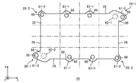
- FIG. 1 is a schematic sectional view illustrating an example of a semiconductor module 100 according to one embodiment of the present invention. It is a figure which shows an example of the shape of the top plate 20 in a top view (xy plane). It is a figure which shows an example of the shape of the case part 40 in a top view (xy plane).
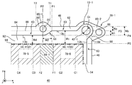
- FIG. 4 is an enlarged view of the vicinity of a first opening part 42-1, a fastening part 85-2, and a first throttle part 68 in FIG.
- FIG. 4 is another enlarged view near the first opening 42-1, the fastening portion 85-2, and the first throttle portion 68 in FIG.
- FIG. 4 is another enlarged view near the first opening 42-1, the fastening portion 85-2, and the first throttle portion 68 in FIG.
- FIG. 4 is a diagram illustrating a center of a bottom plate 64 and a center position of the bottom plate 64 in a second direction in the case unit 40 illustrated in FIG. 3.
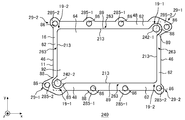
- FIG. 14 is a diagram illustrating a shape of a case section 240 of a comparative example when viewed from above (xy plane).
- FIG. 4 is an enlarged view of a region A in FIG. 3.
- FIG. 9 is a diagram showing an example of an aa ′ cross section in FIG. 8. It is a figure which shows another example of the shape of the case part 40 in a top view (xy plane). It is a figure which shows another example of the shape of the case part 40 in a top view (xy plane). It is the perspective view which showed the top plate 20 and the case part 40 separately. It is a figure showing the outline of vehicles 200 concerning one embodiment of the present invention.
- FIG. 2 is a main circuit diagram of the semiconductor module 100 according to one embodiment of the present invention.
- FIG. 1 is a schematic sectional view showing an example of a semiconductor module 100 according to one embodiment of the present invention.
- the semiconductor module 100 includes a semiconductor device 70 and a cooling device 10.
- the semiconductor device 70 of this example is mounted on the cooling device 10.
- the surface of the cooling device 10 on which the semiconductor device 70 is mounted is defined as an xy plane, and an axis perpendicular to the xy plane is defined as a z-axis.
- the direction from the cooling device 10 toward the semiconductor device 70 in the z-axis direction is referred to as “up”, and the opposite direction is referred to as “down”, but the up and down directions are not limited to the direction of gravity.
- a top view means a case where an object is viewed in the z-axis direction from above the xy plane.
- the semiconductor device 70 includes at least one semiconductor chip 78 such as a power semiconductor chip.
- the semiconductor chip 78 is provided with an insulated gate bipolar transistor (IGBT) formed on a semiconductor substrate such as silicon.
- IGBT insulated gate bipolar transistor
- the semiconductor device 70 has a circuit board 76 and a housing 72.
- the circuit board 76 is, for example, a board in which a circuit pattern is provided on an insulating board.
- the semiconductor chip 78 is fixed to the circuit board 76 via solder or the like.
- the housing 72 is formed of an insulating material such as a resin.
- the accommodation section 72 has an internal space for accommodating the semiconductor chip 78, the circuit board 76, the wiring, and the like.
- the internal space of the housing section 72 may be filled with a sealing section 74 for sealing the semiconductor chip 78, the circuit board 76, the wiring, and the like.
- the sealing section 74 is an insulating member such as a silicone gel or an epoxy resin.
- the cooling device 10 has the top plate 20 and the case 40.
- the top plate 20 may be a plate-shaped metal plate having an upper surface 22 and a lower surface 24 parallel to the xy plane.
- the top plate 20 is formed of a metal including aluminum.
- the semiconductor device 70 is mounted on the upper surface 22 of the top plate 20.
- the heat generated by the semiconductor chip 78 is transmitted to the top plate 20.
- a heat conductive member such as a circuit board 76, a metal plate, and solder is disposed between the top plate 20 and the semiconductor chip 78.
- the circuit board 76 may be directly fixed to the upper surface 22 of the top plate 20 by solder or the like.
- the housing portion 72 is provided so as to surround a region where the circuit board 76 and the like are arranged on the upper surface 22 of the top plate 20.
- the semiconductor device 70 has a metal plate exposed to the internal space of the housing portion 72, a circuit board 76 is fixed on the upper surface of the metal plate, and the metal plate is fixed on the upper surface 22 of the top plate 20. It may be fixed.
- the case part 40 includes a refrigerant circulation part 92 through which the refrigerant circulates, and an outer edge part 62 arranged so as to surround the refrigerant circulation part 92 in the xy plane.
- the outer edge portion 62 is a portion connected to the lower surface 24 of the top plate 20.
- the case section 40 of this example has a bottom plate 64 and a side wall 63.
- the bottom plate 64 is a portion arranged to be spaced apart from the top plate 20 in the z-axis direction so as to face the top plate 20.
- the bottom plate 64 may be arranged parallel to the xy plane.
- the side wall 63 is a portion connecting the outer edge portion 62 and the bottom plate 64.
- the side wall 63 may connect the inner side surface 13 a of the outer edge portion 62 and the peripheral surface of the bottom plate 64.
- the side wall 63 is provided inside the outer edge portion 62.
- the side wall 63 surrounds the refrigerant flow portion inside the outer edge portion 62.
- the outer edge 62, the side wall 63, and the bottom plate 64 may be integrally formed of the same material.
- the outer edge portion 62 and the side wall 63 form the shape (frame shape) of the frame portion 41 provided along the peripheral edge of the bottom plate 64.
- the coolant circulation part 92 is arranged on the lower surface 24 side of the top plate 20.
- the refrigerant distribution section 92 is an area through which a refrigerant such as water flows.
- the coolant circulation part 92 may be a closed space in contact with the lower surface 24 of the top plate 20.
- the case portion 40 is disposed directly or indirectly in close contact with the lower surface 24 of the top plate 20 at the outer edge portion 62. Thereby, the refrigerant circulation part 92 is sealed.
- the upper surface 16 of the outer edge portion 62 is disposed in close or direct contact with the lower surface 24 of the top plate 20. That is, the upper surface 16 of the outer edge portion 62 and the lower surface 24 of the top plate 20 are provided so as to seal the refrigerant flow portion 92.
- the indirect close contact means that the lower surface 24 of the top plate 20 and the case portion 40 are provided via a sealing material, an adhesive, or another member provided between the lower surface 24 of the top plate 20 and the case portion 40. 40 indicates a state in which it is in close contact. Specifically, a sealing material or another member may be provided between the upper surface 16 of the outer edge portion 62 and the lower surface 24 of the top plate 20.
- the close contact indicates a state in which the refrigerant inside the refrigerant flowing portion 92 does not leak from the close contact portion.
- Cooling fins 94 are arranged inside the refrigerant circulation portion 92.
- the cooling fins 94 may be connected to the lower surface 24 of the top plate 20. As the refrigerant passes near the cooling fins 94, heat generated by the semiconductor chip 78 is transferred to the refrigerant. Thereby, the semiconductor device 70 can be cooled.
- the members of the top plate 20 and the case 40 are brazed.
- the top plate 20 and the case portion 40 are formed of a metal having the same composition, and the brazing material is formed of a metal having a lower melting point than the top plate 20 and the like.
- a metal containing aluminum may be used as the metal forming the top plate 20 and the case portion 40.
- an aluminum alloy such as an Al-Mn-based alloy (3000-based aluminum alloy) or an Al-Mg-Si-based alloy (6000-based aluminum alloy) may be used.
- An aluminum alloy such as an Al—Si alloy (4000 aluminum alloy) may be used as the brazing material.
- the bottom plate 64 is disposed so as to have the refrigerant circulation portion 92 between the bottom plate 64 and the lower surface 24 of the top plate 20.
- the bottom plate 64 of the present example is provided with two or more openings 42.
- the opening 42 may include at least one opening for introducing the refrigerant into the refrigerant circulation unit 92 and at least one opening for extracting the refrigerant from the refrigerant circulation unit 92.
- a pipe 90 for transporting the refrigerant is connected to the opening 42.
- the pipe 90 protrudes from the bottom plate 64 on the side opposite to the cooling fins 94 (in this example, the negative side of the z-axis).
- the side wall 63 defines the refrigerant circulation portion 92 by connecting the outer edge portion 62 and the bottom plate 64.
- the inner surface 13a of the outer edge 62 may be the inner peripheral surface of the outer edge 62 in the xy plane.
- the periphery of the bottom plate 64 is an outer peripheral portion of the bottom plate 64 on the xy plane.
- the inner side surface 13a of the outer edge portion 62 may be a side surface facing the refrigerant flow portion 92, and the lower surface of the outer edge portion 62 and the upper surface of the side wall 63 may be connected.
- the top plate 20 and the case portion 40 have a fastening portion 80 for fastening each other.
- the fastening portion 80 may be used to fix the semiconductor module 100 to an external device.
- the fastening portion 80 may be provided at a portion where the top plate 20 and the outer edge portion 62 overlap.
- the fastening portion 80 is a region where the top plate 20 and the case portion 40 are directly or indirectly closely contacted and overlap each other in the z-axis direction, and a through hole 79 penetrating the top plate 20 and the case portion 40. Is a region where the symbol is formed.
- FIG. 1 the area of the top plate 20 in which the through hole 79 is formed and the region of the case portion 40 are indicated by broken lines.
- the fastening portion 80 of this example is provided on the outer edge portion 62.
- FIG. 2 is a diagram illustrating an example of the shape of the top plate 20 as viewed from above (xy plane).
- the top plate 20 has two sets of opposing sides 26 and 28 in a top view.
- the top plate 20 of this example has a substantially rectangular shape having a short side 26 and a long side 28.
- the top plate 20 has four corners 29.
- the direction in which the short side 26 extends is the y-axis
- the direction in which the long side 28 extends is the x-axis.
- a rectangular outer periphery 88 defined by the long side 28 and the short side 26 is defined as an outer periphery of the top plate 20.
- the shape of the outer periphery 88 is a shape in which the projections and depressions on the long sides 28 and the short sides 26 of the top plate 20 are replaced with the extension lines of the long sides 28 and the short sides 26.
- the outer periphery 88 is indicated by a broken line.
- the corner 29 indicates a region near each vertex in the outer periphery 88 of the top plate 20.
- the outer periphery 88 of the top plate 20 is arranged at the corner of the outer periphery 88 among 16 regions formed by dividing the outer periphery 88 into four in each of the x-axis and the y-axis.
- One area is defined as a corner 29.
- the corner 29 disposed opposite the opening 42 of the case 40 is referred to as a first corner 29-1, and the other corner 29 is referred to as a second corner 29-2.
- the top plate 20 is provided with one or more fastening portions 81 which are a part of the fastening portions 80 shown in FIG.
- the fastening portion 81-1 is provided so as to overlap the side 28.
- the fastening portions 81-2 are provided at the corners 29-1 and 29-2.
- Each fastening portion 81 has a through hole 86 which is a part of the through hole 79 shown in FIG.
- the through hole 86 may be arranged outside the outer periphery 88, may be arranged inside the outer periphery 88, or may be arranged so as to overlap the outer periphery 88.
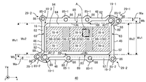
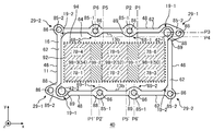
- FIG. 3 is a diagram showing an example of the shape of the case section 40 when viewed from above (xy plane).
- the outer shape of the outer edge 62 corresponds to the outer shape of the case 40.
- the case section 40 has two pairs of opposed sides 46 and 48 when viewed from above.
- the sides 46 and 48 may mean sides of the outer shape of the case section 40 in a top view.
- the case section 40 of the present example has a substantially rectangular shape having a short side 46 and a long side 48.
- the case portion 40 includes a bottom plate 64 having four corner portions 19.
- the corner 19 indicates a region near each vertex on the outer periphery 89 of the case 40.
- At least one corner 19 is provided with an opening 42 for connecting the refrigerant flow portion 92 to the outside.
- the corner 19 where the opening 42 is arranged is a first corner 19-1 and the other corners 19 are a second corner 19-2.
- a first opening 42-1 is provided in one first corner 19-1
- a second opening 42 is provided in another one first corner 19-1. -2 is provided.
- the first corner 19-1 may include the entirety of the opening 42 or only a part thereof.
- a region of the outer periphery 88 facing the opening 42 is indicated by a broken line.
- the side 26 of the top plate 20 and the side 46 of the case 40 overlap in a top view.
- the side 28 of the top plate 20 and the side 48 of the case portion 40 overlap in a top view. That is, the outer shape of the case section 40 in the xy plane of the present example is the same as the outer shape of the top plate 20. Also, in FIG. 3, the outer periphery 88 of the top plate 20 is shown overlapping the shape of the case section 40.
- the corner 19 of the bottom plate 64 and the corner 29 of the top plate 20 may be arranged to face each other. More specifically, a corner 19-1 on the positive side of the x-axis and the positive side of the y-axis and a corner 29-1 on the positive side of the x-axis and the positive side of the y-axis may be arranged to face each other.
- the corner 19-2 on the positive side of the x-axis and the negative side of the y-axis and the corner 29-2 on the positive side of the x-axis and the negative side of the y-axis may be arranged to face each other.
- the corner 19-2 on the negative side of the x-axis and the positive side of the y-axis and the corner 29-2 on the negative side of the x-axis and the positive side of the y-axis may be arranged to face each other.
- the corner portion 19-1 on the negative side of the x-axis and the negative side of the y-axis and the corner portion 29-1 on the negative side of the x-axis and the negative side of the y-axis may be arranged to face each other.
- the outer edge portion 62 has an inner surface 13a on the refrigerant circulation portion 92 side and an outer surface 11 on the opposite side to the inner surface 13.
- Each side surface in this example is a surface substantially perpendicular to the xy plane.
- the inner side surface 13 b of the side wall 63 is a side surface facing the refrigerant flow portion 92.
- the side wall 63 adjusts the width of the coolant circulation portion 92 in a first direction (in this example, the y-axis direction) parallel to the pair of opposed sides 46 in a second direction (in this example) orthogonal to the first direction when viewed from above.
- the width in the first direction of the refrigerant flow portion 92 between the first opening portion 42-1 and the first throttle portion 68 is Wv1
- the x-axis negative side of the first throttle portion 68 Assuming that the width of the refrigerant flow portion 92 in the first direction at the opposite side to the first opening 42-1 is Wv2, the first throttle portion 68 sets the width of the refrigerant flow portion 92 to the second width.
- the width Wv1 is changed from the width Wv1 to the width Wv2 along the direction.
- the width Wv2 is smaller than the width Wv1.
- the outer periphery 89 includes an extension of the inner side surface 13b between the first opening 42-1 and the first throttle portion 68 in the second direction, and the second opening 42- in the second direction. It is a rectangular shape in a top view, defined by an extension of the inner surface 13b between the second and second throttle portions 69 and an extension of a pair of inner surfaces 13b parallel to the side 46.
- the width in the y-axis direction of the outer edge portion 62 on the side of the first opening 42-1 with respect to the first aperture portion 68 is defined as a width Wa.
- the width in the y-axis direction of the outer edge portion 62 on the opposite side of the first aperture portion 68 from the first opening portion 42-1 is defined as a width Wb.
- the width Wa is smaller than the width Wb. That is, the width of the outer edge portion 62 is different before and after the first throttle portion 68 in the x-axis direction. At the outer edge 62 on the side opposite to the first opening 42-1 with respect to the first aperture portion 68, the outer periphery 89 and the outer edge 62 may overlap in a top view.
- the width of the outer edge portion 62 in the first throttle portion 68 in the y-axis direction may continuously change from the width Wa to the width Wb along the x-axis direction.
- the inner side surface 13b of the first throttle portion 68 may have a curved shape when viewed from above.
- the side wall 63 may include a second throttle unit 69 provided on a side facing the first throttle unit 68 with the bottom plate 64 interposed therebetween.
- the second throttle section 69 changes the width of the refrigerant flow section 92 in the first direction along the second direction when viewed from above.
- the width in the first direction of the refrigerant flow portion 92 between the second opening 42-2 and the second throttle portion 69 may be the width Wv1.
- the width of the refrigerant flow portion 92 in the first direction on the x-axis positive side of the second throttle portion 69 (ie, on the side opposite to the second opening 42-2) may be the width Wv2.
- the second throttle portion 69 changes the width of the refrigerant flow portion 92 from the width Wv1 to Wv2 along the second direction.
- the width of the refrigerant flowing portion 92 in the first direction is a width Wv1 between the first opening 42-1 and the first throttle portion 68 along the second direction, and the width Wv1 of the second direction from the first throttle portion 68.
- the width Wv2 may be between the second throttle portion 69 and the second opening 42-2.
- the width of the outer edge 62 in the y-axis direction on the second opening 42-2 side of the second throttle portion 69 may be the width Wa.
- the width in the y-axis direction of the outer edge portion 62 on the opposite side of the second aperture portion 69 from the second opening portion 42-2 may be the width Wb.
- the width of the outer edge portion 62 is different before and after the second throttle portion 69 in the x-axis direction.
- the outer periphery 89 and the outer edge 62 may overlap in a top view.
- the width of the outer edge portion 62 in the second throttle portion 69 in the y-axis direction may be continuously changed from the width Wa to the width Wb along the x-axis direction.
- the inner side surface 13 of the second throttle section 69 may have a curved shape when viewed from above.
- FIG. 3 shows an example of the arrangement of the cooling fins 94 and the semiconductor chips 78 as viewed from above.
- the cooling fins 94 are arranged in a region indicated by a thick broken line in FIG.
- two semiconductor chips 78 are arranged in the first direction (y-axis direction) and three in the second direction (x-axis direction).
- the cooling fin 94 may have a first path 98 and a second path 99 provided along the first direction (y-axis direction).
- the second path 99 may have a larger pressure loss per unit area into which the refrigerant flows than the first path 98.
- the first path 98 may be arranged to include the object to be cooled (that is, the semiconductor chip 78) when viewed from above. Further, the second path 99 may be arranged between two cooled objects (ie, the semiconductor chips 78) adjacent in the x-axis direction.
- the side wall 63 includes the first throttle portion 68, when the refrigerant flowing from the first opening 42-1 reaches the first throttle portion 68, the pressure of the refrigerant increases.
- the amount of the refrigerant flowing in the first direction in which the object to be cooled (the semiconductor chip 78 in this example) is arranged increases. Therefore, the cooling efficiency of the semiconductor module 100 can be improved. Therefore, the power conversion capability of the semiconductor module can be improved.
- the case section 40 is provided with one or more fastening sections 85 which are a part of the fastening section 80 shown in FIG.
- the fastening portion 85-1 is provided so as to overlap the side 48.
- the fastening portions 85-2 are provided at the corners 29-1 and 29-2.
- Each fastening portion 85 is provided so as to protrude outside the outer periphery 89 of the case portion 40.
- Each fastening portion 85 has a through hole 86 which is a part of the through hole 79 shown in FIG.
- the through hole 86 may be arranged outside the outer periphery 89, may be arranged inside the outer periphery 89, or may be arranged so as to overlap the outer periphery 89.
- the second throttle portion 69 may be provided downstream of the second flow path 99-1 and the second path 99-2 in the refrigerant flow path in the refrigerant flow section 92. That is, when the refrigerant is introduced from the first opening 42-1 and is derived from the second opening 42-2, the refrigerant introduced from the first opening 42-1 flows through the second path 99-. After passing through the first and second paths 99-2, the second throttle section 69 may be reached.
- the semiconductor chip 78 may be arranged in the first area 50, the second area 52, and the third area 54 from the upstream side of the circulation path of the refrigerant circulation unit 92.
- the first throttle section 68 may be arranged between the first area 50 and the second area 52 in the second direction.
- the refrigerant bends the flow path in the second direction by the first throttle portion 68. Can be Therefore, the refrigerant easily passes between the semiconductor chips 78 in the second direction. Therefore, the cooling efficiency of the semiconductor module 100 can be improved.
- the semiconductor module 100 of the present embodiment can reduce the capacity of the refrigerant circulation device. For this reason, the cost of the refrigerant circulation device can be reduced. Further, the size of the refrigerant circulation device can be reduced.
- FIG. 4 is an enlarged view of the vicinity of the first opening 42-1, the fastening portion 85-2, and the first throttle portion 68 in FIG.
- the position of the inner surface 13 in the second direction where the width of the refrigerant flow portion 92 starts to decrease from the width Wv1 (see FIG. 3) is defined as a position P1
- the position of the position P1 in the first direction is defined as a position P3.
- the position in the second direction of the inner side surface 13 at which the width of the refrigerant flow portion 92 starts increasing from Wv2 (see FIG. 3) in the positive x-axis direction is defined as position P2, and the position of the position P2 in the first direction is defined as position P2.
- P4 The position in the second direction of the inner side surface 13 at which the width of the refrigerant flow portion 92 starts increasing from Wv2 (see FIG. 3) in the positive x-axis direction
- the first throttle section 68 may point to the side wall 63 between the position P1 and the position P2 in the second direction.
- the position P1 and the position P2 are end positions of the first throttle unit 68 in the second direction, respectively.
- the width W2 is the width of the first throttle section 68 in the second direction.
- the position P3 and the position P4 are end positions of the first throttle unit 68 in the first direction, respectively.
- the width W1 is the width of the first throttle section 68 in the first direction.
- the width Wb is equal to the sum of the width Wa and the width W1.
- the position P1 and the position P2 of the side wall 63 may be provided on the downstream side (x-axis negative side) with respect to the first region 50.
- the position P1 of the side wall 63 may be provided to face the second path 99-1 in the first direction with the refrigerant flowing portion 92 interposed therebetween.
- the position of the end of the fastening portion 85-1 on the positive side of the x-axis is position T1
- the position of the end of the fastening portion 85-1 on the negative side of the x-axis is position T2.
- One fastening portion 85-1 is arranged facing the first throttle portion 68 in the first direction.
- the fastening portion 85-1 is arranged to face the first throttle portion 68 in the first direction when the region where the fastening portion 85-1 is provided is extended in the first direction when viewed from above.
- At least a part of the extended area overlaps the first throttle section 68. That is, it means that at least a part of the region in the x-axis direction between the position P1 and the position P2 and at least a part of the region in the x-axis direction between the position T1 and the position T2 overlap.
- the fastening portion 85-1 may be provided at a position overlapping the outer periphery 89. That is, the fastening portion 85-1 moves the inner side surface 13 of the side wall 63 provided between the first throttle portion 68 and the first opening portion 42-1 at a position overlapping with an extension line extending in the x-axis direction. May be provided.
- the fastening portion 85-1 may be arranged such that half or more of the region is located outside the extension line (positive y-axis side) or inside the extension line (negative y-axis side). .
- the first aperture portion 68 may be provided to have a smooth curve that changes continuously when viewed from above.
- the first throttle section 68 may include a curve that is convex in the first direction.
- the refrigerant can be smoothly guided in the first direction by the first throttle portion 68 having a smooth curved shape.
- the curvature of the first throttle portion 68 provided in a curved shape may be larger than the curvature of the arc of the through hole 86.
- the fastening portion 85-1 is disposed to face the first throttle portion 68 in the first direction, the fastening portion 85 is moved in the center direction of the bottom plate in the first direction (see FIG. In FIG. 4, it can be arranged on the y-axis negative side). Therefore, the size of the semiconductor module 100 can be reduced. Therefore, the cost of the semiconductor module 100 can be reduced.
- the position P5 is the end on the y-axis negative side of the flow path of the refrigerant introduced from the first opening 42-1 and traveling in the x-axis negative direction when the first throttle unit 68 is not provided. It is.
- the width Wc is the width in the y-axis direction from the position P3 to the position P5. That is, when the first throttle unit 68 is not provided, the refrigerant introduced from the first opening 42-1 advances in the x-axis negative direction at the width Wc.
- the width Wd is the width in the y-axis direction from the position P4 to the position P5.
- the width of the flow path of the refrigerant introduced from the first opening portion 42-1 is reduced by the first throttle portion 68.
- the width Wc is equal to the sum of the width W1 and the width Wd.
- the width Wd may be 2 or less of the width Wc.
- the width Wd may be ⁇ or less of the width Wc, or ⁇ or less. As the width Wd is smaller than the width Wc, the refrigerant more easily moves toward the negative side of the y-axis.
- the semiconductor module 100 has a plurality of semiconductor chips 78 mounted thereon, it is important to appropriately distribute the flow rate of the refrigerant in order to cool each semiconductor chip 78 in a well-balanced manner.
- the size of the width Wd it is possible to control the flow rate of the refrigerant to the negative side of the y-axis where the object to be cooled (the semiconductor chip 78) is provided. Thereby, the cooling balance of the semiconductor chip 78 can be adjusted.
- the position of the end of the second path 99-1 on the positive side of the x-axis is defined as position F1
- the position of the end of the second path 99-1 on the negative side of the x-axis is defined as position F2.
- the first direction y-axis direction
- at least a part of the second path 99-1 in the second direction may be arranged to face the first throttle section 68.
- the second path 99-1 is disposed so as to face the first throttle section 68. This means that, in a top view, the area where the second path 99-1 is provided extends in the first direction. When extended, it indicates that at least a part of the extended area overlaps the first throttle unit 68.
- the cooling device 10 of the present example at least a part of the second path 99-1 in the second direction (x-axis direction) faces the first throttle unit 68 in the first direction (y-axis direction). Since the refrigerant is disposed, the refrigerant whose flow path is bent in the first direction by the first throttle unit 68 easily passes through the first path 98-1. Therefore, the cooling efficiency of the semiconductor module 100 can be improved.
- the first throttle portion 68 When the refrigerant is introduced from the first opening 42-1, the first throttle portion 68 is located at a position closer to the refrigerant flow portion than the semiconductor chip 78-6 disposed on the most upstream side of the flow path of the refrigerant flow portion 92. It may be located downstream of the 92 distribution channels. That is, in the x-axis direction, the position P1 may be located on the x-axis negative side of the semiconductor chip 78-6.
- the position of the end of the semiconductor chip 78-6 on the positive side of the x axis is defined as a position C1, and the position of the end of the semiconductor chip 78-6 on the negative side of the x axis is defined as a position C2.
- the end position of the semiconductor chip 78-5 on the positive side of the x axis is defined as a position C3, and the end position of the semiconductor chip 78-5 on the negative side of the x axis is defined as a position C4.
- the semiconductor chip 78 and the first throttle section 68 do not need to be arranged to face each other.
- the semiconductor chip 78 and the first aperture portion 68 are not disposed so as to face each other.
- the extended region does not overlap the first throttle section 68. That is, it indicates that the region in the x-axis direction between the position P1 and the position P2 does not overlap with the region in the x-axis direction between the position C1 and the position C2. It also indicates that the region in the x-axis direction between the position P1 and the position P2 does not overlap with the region in the x-axis direction between the position C3 and the position C4.
- the refrigerant whose flow path is bent in the first direction by the first throttle portion 68 becomes a semiconductor in the second direction. It becomes easier to pass between the chips 78. Therefore, the cooling efficiency of the semiconductor module 100 can be improved.
- the through hole 86 may be provided on the center side of the case portion 40 in the first direction with respect to the side wall 63 between the position P1 in the x-axis direction and the corner portion 19-1.
- at least a part of the through-hole 86 may be provided between the position P3 and the position P4 in a top view. That is, in a top view, the through-hole 86 and the outer periphery 89 may overlap.
- the through hole 86 provided in the fastening portion 85-1 and the outer periphery 89 overlap.
- the first opening 42-1 may be disposed outside the case section 40 in the first direction with respect to the first throttle section 68. That is, the end position of the first opening 42-1 on the y-axis negative side may be located on the y-axis positive side from the position P4. Since the first opening 42-1 is disposed outside the case 40 in the first direction with respect to the first throttle section 68, the first opening 42-1 is introduced from the first opening 42-1 and the x-axis negative side The refrigerant that has proceeded in the direction easily reaches the first throttle portion 68.
- the diameter of the first opening 42-1 is Di, and the width of the first aperture portion 68 in the first direction (y-axis direction) is W1.
- the diameter Di may be 0.5 times or more and 2 times or less of the width W1.
- FIG. 5 is another enlarged view of the vicinity of the first opening 42-1, the fastening portion 85-2, and the first throttle portion 68 in FIG.
- the position P4 ' is a position in the y-axis direction of the side wall 63 on the x-axis negative side of the first throttle section 68.
- the position P5 ′ is the end on the y-axis negative side of the flow path of the refrigerant introduced from the first opening 42-1 and traveling in the x-axis negative direction when the first throttle unit 68 is not provided. is there.
- the width Wc ' is a width in the y-axis direction from the position P3 to the position P5'.
- the width W1 ' is a width in the y-axis direction from the position P3 to the position P4'.
- the width Wb ′ is a width in the y-axis direction of the outer edge portion 62 on the opposite side of the first aperture portion 68 from the first opening portion 42-1.
- the width Wa ′ is the width in the y-axis direction of the outer edge portion 62 on the first opening 42-1 side with respect to the first aperture portion 68.
- the whole of the through hole 86 provided in the fastening portion 85-1 is, as viewed from above, the case in the first direction more than the side wall 63 between the position P1 in the x-axis direction and the corner 19-1. It is provided on the center side of the part 40.
- the whole of the through hole 86 is provided between the position P3 and the position P4 ′ when viewed from above.
- the end on the y-axis positive side of the through hole 86 is disposed on the y-axis negative side from the position P3.
- the end on the y-axis negative side of the through hole 86 is disposed on the y-axis positive side from the position P4 '.
- the diameter of the through hole 86 is smaller than the width W1 ′.
- the entirety of the through hole 86 provided in the fastening portion 85-1 is higher than the side wall 63 between the position P1 in the x-axis direction and the corner 19-1 in the top view.
- the through-hole 86 is provided on the center side of the case portion 40 in the y-axis direction (the y-axis negative side in the example of FIG. 5) as compared with the example shown in FIG. can do.
- the cooling device 10 of the present example can further reduce the width of the case portion 40 in the y-axis direction as compared with the example shown in FIG. Therefore, the size of the semiconductor module 100 can be further reduced as compared with the example shown in FIG. Therefore, the cost of the semiconductor module 100 can be reduced.
- FIG. 6 is a view showing the center of the bottom plate 64 and the center position of the bottom plate 64 in the second direction in the case section 40 shown in FIG. 6, the cooling fins 94, the first path 98 and the second path 99, the first area 50, the second area 52 and the third area 54, and the semiconductor chip 78 are omitted for the sake of visibility of the drawing. Is shown.
- the center of the circular first opening 42-1 is the position of the first opening 42-1.
- the midpoint Pm between the position P1 and the position P2 in the second direction is defined as the position of the first throttle section 68 in the second direction. (That is, in the second direction, the distance between the position P1 and the position Pm and the distance between the position P2 and the position Pm are both (1/2) W2.)
- the center position of the bottom plate 64 in the second direction is determined. It is assumed that the position is Cx.
- the distance Dh1 is a distance in the second direction from the first opening 42-1 to the first diaphragm 68.
- the distance Dh2 is a distance from the first opening 42-1 to the position Cx in the second direction.
- the distance Dh1 may be shorter than the distance Dh2. Since the distance Dh1 is shorter than the distance Dh2, the refrigerant introduced from the first opening 42-1 is easily distributed evenly to the entire bottom plate 64.
- the center of the bottom plate 64 as viewed from above is the center C.
- the center C may be a point where two diagonals of the outer circumference 89 intersect.
- the center C may be a point where two diagonal lines of the outer periphery 89 intersect.
- the first opening 42-1 and the second opening 42-2 may be arranged symmetrically (point-symmetrically) with respect to the center C of the bottom plate 64 when viewed from above.
- the first throttle unit 68 and the second throttle unit 69 may be arranged symmetrically (point-symmetrically) with respect to the center C of the bottom plate 64 as viewed from above.
- the first opening 42-1 and the second opening 42-2 are arranged symmetrically with respect to the center C of the bottom plate 64, and the first diaphragm 68 and the second diaphragm 69 are arranged at the center C of the bottom plate 64.
- the nodes of the vibration in the first opening 42-1 and the second opening 42-2 easily overlap with the antinode. For this reason, the mechanical strength of the case part 40 can be increased.
- the semiconductor module 100 can be similarly cooled regardless of which of the first opening 42-1 and the second opening 42-2 is used as the inlet and the outlet of the refrigerant.
- FIG. 7 is a diagram illustrating a shape of the case portion 240 of the comparative example as viewed from above (xy plane).
- the case section 240 of the comparative example does not include the first throttle section 68 and the second throttle section 69 of the case section 40 of the present example shown in FIG.
- the side wall 263 does not include the first throttle section 68, the refrigerant that has flowed in from the opening section 242 and has started flowing in the negative x-axis direction flows in the first direction (y-axis direction). It is easy to flow in the x-axis negative direction without changing the direction. Therefore, the amount of the refrigerant flowing in the direction of the object to be cooled disposed near the center of the bottom plate 64 when viewed from above is reduced. For this reason, it is difficult to improve the cooling efficiency of the semiconductor module incorporating the case 240.
- the fastening portion 285-1 in the first direction is shown in FIG. It must be arranged outside the case section 40 of the present example shown. For this reason, the width of the case portion 240 in the first direction must be larger than that of the case portion 40 in the example of FIG. For this reason, it is difficult to reduce the size of the semiconductor module 100 in which the case 240 is incorporated.
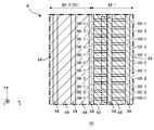
- FIG. 8 is an enlarged view of the area A in FIG.
- each cooling fin 94 is provided along the y-axis direction.
- the refrigerant introduced from the first opening 42-1 flows between the cooling fins 94 adjacent in the x-axis direction from the positive side of the y-axis to the negative side of the y-axis along the y-axis direction. Flowing.
- a resistor 96 is provided between the cooling fins 94 adjacent in the x-axis direction, for example.
- the first resistor 96-1 is provided, for example, in contact with the bottom plate 64 in the z-axis direction.
- the second resistor 96-2 is provided, for example, in contact with the lower surface 24 of the top plate 20 in the z-axis direction.
- the resistor 96 may not be provided in the first path 98-2.
- the first resistor 96-1 and the second resistor 96-2 may be provided between the cooling fins 94 adjacent in the x-axis direction.
- the first resistor 96-1 and the second resistor 96-2 may be in contact with the cooling fin 94 at both ends in the x-axis direction.
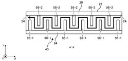
- FIG. 9 is a diagram showing an example of a section taken along the line aa ′ in FIG.
- the first resistor 96-1 and the second resistor 96-2 are alternately arranged in the y-axis direction in the second path 99-1.
- the first resistor 96-1 is provided in contact with the bottom plate 64 and is provided separately from the lower surface 24 of the top plate 20.
- the second resistor 96-2 is provided in contact with the lower surface 24 of the top plate 20, and is provided separately from the bottom plate 64.
- the first resistor 96-1 and the second resistor 96-2 may be provided so as to overlap in the z-axis direction.
- the path of the refrigerant introduced from the first opening 42-1 is indicated by a thick arrow.
- the refrigerant flows between the top plate 20 and the first resistor 96-1 in the z-axis direction and between the first resistor 96-1 and the second resistor 96-2.
- the air flows from the negative side of the y-axis toward the positive side of the y-axis in the axial direction and between the bottom plate 64 and the second resistor 96-2 in the z-axis direction.
- the first resistor 96-1 and the second resistor 96-2 are provided in the second path 99-1, they are introduced from the first opening 42-1.
- the cooled refrigerant is less likely to flow from the positive side of the y-axis toward the negative side of the y-axis in the second path 99-1 than in the first path 98-2. That is, the second path 99-1 has a larger pressure loss per unit area into which the refrigerant flows than the first path 98-2. Therefore, the refrigerant flows more easily in the first path 98-2 than in the second path 99-1. For this reason, the cooling efficiency of the semiconductor chip 78 can be improved.
- FIG. 10 is a diagram showing another example of the shape of the case section 40 when viewed from above (xy plane).
- the case 40 shown in FIG. 10 differs from the case 40 shown in FIG. 3 in that the side wall 63 includes a plurality of first throttles 68 and second throttles 69, respectively.
- the side wall 63 includes two first throttle portions 68 and two second throttle portions 69, respectively.
- the first throttle portion 68 of this example is provided on one side wall 63 parallel to the long side 48.
- the second throttle portion 69 of this example is provided on the other side wall 63 opposite to the one side wall 63 in a top view.
- the side wall 63 further includes a first throttle section 68-2 and a second throttle section 69-2 as compared with the case section 40 shown in FIG.
- One fastening portion 85-1 is arranged to face the first throttle portion 68-2 in the first direction (y-axis direction).
- the other one of the fastening portions 85-1 is arranged to face the second throttle portion 69-2 in the first direction.
- the two end positions of the first aperture portion 68-2 in the second direction are referred to as position P5 and position P6, respectively.
- position P5 and position P6 are referred to as position P5 and position P6, respectively.
- at least a part of the second path 99-2 in the first direction may overlap the first throttle section 68-2. That is, at least a part of the range from the position P5 to the position P6 in the second direction of the first aperture portion 68-2 may overlap the second path 99-2 in the first direction.
- the two end positions of the second throttle portion 69-2 in the second direction are referred to as position P5 'and position P6', respectively.
- position P5 'and position P6' In the second direction (x-axis direction), at least a part of the second path 99-1 in the first direction (y-axis direction) may overlap the second throttle section 69-2. That is, at least a part of the range from the position P5 'to the position P6' in the second direction of the second throttle portion 69-2 may overlap the second path 99-1 in the first direction.
- the position P6 ′ may be located on the x-axis positive side of the position P2, and the position P6 may be located on the x-axis negative side of the position P2 ′.
- a line segment connecting the first throttle unit 68-1 (position P2) and the second throttle unit 69-2 (position P6 ′) disposed with the second path 99-1 interposed therebetween is an x-axis. It may be inclined with respect to the y-axis in a direction from the positive side toward the y-axis positive side.
- a line segment connecting the first throttle unit 68-2 (position P6) and the second throttle unit 69-1 (position P2 ′) arranged with the second path 99-2 interposed therebetween is an x-axis.
- the side wall 63 includes a plurality of first throttle portions 68. For this reason, of the refrigerant flowing from the first opening 42-1 and reaching the first throttle portion 68-1, the path is not bent by the first throttle portion 68-1 and moves in the x-axis negative direction. The refrigerant that has continued to flow easily passes through the second path 99-2 by the first throttle section 68-2. For this reason, the cooling efficiency of the semiconductor module 100 can be further improved as compared with the case section 40 shown in FIG. Note that the side wall 63 may include three or more first throttle portions 68 and two or more second throttle portions 69.
- FIG. 11 is a diagram showing another example of the shape of the case section 40 when viewed from above (xy plane).
- the width in the first direction (y-axis direction) of one first throttle section 68-1 closest to the first opening 42-1 is set. 10 is different from the case section 40 shown in FIG. 10 in that the width of the other first throttle section 68-2 in the first direction is larger. That is, in the case portion 40 shown in FIG. 11, the first throttle portion 68-1 and the second throttle portion 69-1 are different from the first throttle portion 68-1 and the second throttle portion 68-1 in the case portion 40 shown in FIG. It is larger in the first direction (y-axis direction) than the throttle section 69-1.
- the two end positions of the first throttle unit 68-1 are referred to as positions P3 and P4 ', respectively.
- the width W1 ′′ is the width in the first direction between the position P3 and the position P4 ′.
- the width W1 ′′ is larger than the width W1.
- the width of the second throttle portion 69-1 in the first direction may be equal to the width W1 ''.
- the widths of the first throttle portion 68-1 and the second throttle portion 69-1 in the first direction may be other than the width W1 and the width W1 ′.
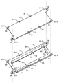
- FIG. 12 is a perspective view showing the top plate 20 and the case section 40 separately.
- the top plate 20 and the case portion 40 may have substantially the same outer shape in the xy plane.
- Each fastening portion of the top plate 20 and the case portion 40 may have the same shape in the xy plane, and may be arranged so as to overlap in the z-axis direction.
- the position where the top plate 20 and the case portion 40 overlap when the top plate 20 and the case portion 40 are fixed by brazing or the like is indicated by broken lines. Note that, in FIG. 12, the cooling fins 94 arranged in the coolant circulation part 92 are omitted. Also, the brazing material between the members is omitted.
- the outer edge 62 of the case 40 is fixed to the top plate 20.
- the case section 40 has a bottom plate 64 disposed apart from the top plate 20, and a side wall 63 connecting the bottom plate 64 and the outer edge portion 62.
- the lower surface 24 of the top plate 20 and the case portion 40 define a coolant circulation portion 92.
- the fastening portion 80 is provided on the outer periphery 88 of the top plate 20 so as to protrude outward on the side opposite to the opening portion 42 and the corner portion 19 (see FIG. 3) of the bottom plate 64. Further, in the fastening portion 80, the outer edge portion 62 and the top plate 20 are stacked in order, and have a through hole 79 (see FIG. 1) penetrating the outer edge portion 62 and the top plate 20.
- the through hole 86 provided in the top plate 20 and the through hole 86 provided in the case portion 40 may be provided coaxially with each other.
- the top plate 20 and the case part 40 may have the same thickness.
- the top plate 20 and the case portion 40 may have the same thickness in a region other than the fastening portion 80.
- the case portion 40 may be provided with the outer edge portion 62 and the side wall 63 integrally.
- the outer edge portion 62 and the side wall 63 may be formed by forging a single sheet of metal.
- the bottom plate 64 may be provided integrally with the side wall 63, and may be brazed to the side wall 63.
- the bottom plate 64, the outer edge 62, and the side wall 63 may have the same thickness.
- the thickness of the bottom plate 64 at a position facing the center of the lower surface 24 of the top plate 20 and the thickness of the outer edge 62 of the fastening portion 80 may be the same. Since each member has the same thickness, the cooling device 10 can be manufactured using a common metal roll material.
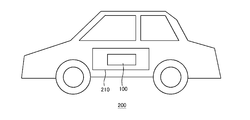
- FIG. 13 is a diagram showing an outline of a vehicle 200 according to one embodiment of the present invention.
- the vehicle 200 is a vehicle that generates at least a part of propulsion using electric power.
- the vehicle 200 is an electric vehicle that generates all propulsion power by a power drive device such as a motor, or a hybrid vehicle that uses both a power drive device such as a motor and an internal combustion engine driven by fuel such as gasoline. .
- the vehicle 200 includes a control device 210 (external device) that controls a power drive device such as a motor.
- the control device 210 includes the semiconductor module 100.
- the semiconductor module 100 may control the power supplied to the power driving device.
- FIG. 14 is a main circuit diagram of the semiconductor module 100 according to one embodiment of the present invention.
- the semiconductor module 100 may be a part of a vehicle-mounted unit that drives a motor of a vehicle.
- the semiconductor module 100 may function as a three-phase AC inverter circuit having output terminals U, V, and W.
- the semiconductor chip 78-1, the semiconductor chip 78-2, and the semiconductor chip 78-3 may constitute a lower arm in the semiconductor module 100.
- the semiconductor chip 78-4, the semiconductor chip 78-5, and the semiconductor chip 78-6 may form an upper arm in the semiconductor module 100.
- One set of the semiconductor chip 78-1 and the semiconductor chip 78-4 may constitute a leg.
- the set of semiconductor chips 78-2 and 78-5 may similarly constitute a leg.
- the pair of semiconductor chips 78-3 and 78-6 may similarly constitute a leg.
- the emitter electrode may be electrically connected to the input terminal N1, and the collector electrode may be electrically connected to the output terminal U.
- the emitter electrode may be electrically connected to the output terminal U, and the collector electrode may be electrically connected to the input terminal PP1.
- the emitter electrode may be electrically connected to the input terminal N2, and the collector electrode may be electrically connected to the output terminal V.
- the emitter electrode may be electrically connected to the output terminal V, and the collector electrode may be electrically connected to the input terminal PP2.
- the emitter electrode may be electrically connected to the input terminal N3, and the collector electrode may be electrically connected to the output terminal W.
- the emitter electrode may be electrically connected to the output terminal W, and the collector electrode may be electrically connected to the input terminal PP3.
- the semiconductor chips 78-1 to 78-6 may be alternately switched by a signal input to the control electrode pad of the semiconductor chip 78.
- each semiconductor chip 78 may generate heat during switching.
- the input terminals PP1, PP2 and PP3 may be connected to the positive pole of the external power supply, and the input terminals N1, N2 and N3 may be connected to the negative pole of the external power supply.
- the output terminals U, V and W may each be connected to a load.
- the input terminals PP1, PP2 and PP3 may be electrically connected to each other. Further, the other input terminals N1, N2 and N3 may be electrically connected to each other.
- the semiconductor chips 78-1 to 78-6 may be RC-IGBT (reverse conducting IGBT) semiconductor chips.
- the IGBT and the free wheel diode (FWD) may be integrally formed, and the IGBT and the FWD may be connected in anti-parallel.
- Each of the semiconductor chips 78-1 to 78-6 may include a combination of a transistor such as a MOSFET or an IGBT and a diode.
- the transistor and diode chip substrates may be silicon substrates, silicon carbide substrates or gallium nitride substrates.
- Reference Signs List 10 cooling device 11 outer surface, 13a inner surface, 13b inner surface, 16 upper surface, 19 corner portion, 20 top plate, 22 ..Upper surface, 24 lower surface, 26 side, 28 side, 29 corner, 40 case, 41 frame, 42 opening 46 ... side, 48 ... side, 50 ... first area, 52 ... second area, 54 ... third area, 62 ... outer edge, 63 ... side wall, 64 ... bottom plate, 68 ... first throttle unit, 69 ... second throttle unit, 70 ... semiconductor device, 72 ... housing unit, 74 ...
- sealing unit 76 ... ⁇ Circuit board, 78 ⁇ ⁇ ⁇ Semiconductor chip, 79 ⁇ ⁇ ⁇ Through hole, 80 ⁇ ⁇ ⁇ Fastening portion, 81 ⁇ ⁇ ⁇ Fastening portion, 85 ⁇ ⁇ ⁇ Fastening portion, 86 ⁇ ⁇ ⁇ Through hole, 88 ⁇ ⁇ ⁇ Outer circumference, 89 ... outer circumference, 0 ... pipe, 92 ... refrigerant circulation part, 94 ... cooling fin, 96 ... resistor, 98 ... path, 99 ... path, 100 ... semiconductor module, 200 ... -Vehicle, 210-Control device, 263-Side wall, 240-Case part, 242-Opening, 285-Fastening part
Landscapes
- Engineering & Computer Science (AREA)
- Microelectronics & Electronic Packaging (AREA)
- Physics & Mathematics (AREA)
- Thermal Sciences (AREA)
- Cooling Or The Like Of Semiconductors Or Solid State Devices (AREA)
- Cooling Or The Like Of Electrical Apparatus (AREA)
Abstract
半導体チップを含む半導体モジュール用の冷却装置であって、下面を有する天板と、天板の下面側に配置されて冷媒を流通するための流通部、流通部を囲む外縁部、および外縁部の内側に設けられた側壁を含み、上面視で2組の対向する辺を有するケース部とを備え、側壁は上面視で1組の対向する辺に平行な第1方向における流通部の幅を第1方向と直交する第2方向に沿って変化させる第1の絞り部を含み、天板およびケース部を外部装置に締結するための締結部が天板およびケース部は天板および外縁部が重なって配置された部分に設けられ、締結部は第1方向に第1の絞り部に対向して配置される、冷却装置を提供する。
Description
本発明は、冷却装置、半導体モジュールおよび車両に関する。
従来、パワー半導体チップ等の半導体素子を含む半導体モジュールにおいて、冷却装置を設けた構成が知られている(例えば、特許文献1-5参照)。
特許文献1 国際公開第2016/204257号
特許文献2 国際公開第2016/021565号
特許文献3 特開2014-179563号公報
特許文献4 特開2015-65310号公報
特許文献5 特許第5565459号公報
特許文献1 国際公開第2016/204257号
特許文献2 国際公開第2016/021565号
特許文献3 特開2014-179563号公報
特許文献4 特開2015-65310号公報
特許文献5 特許第5565459号公報
冷却装置は、小型化が容易な構造を有することが好ましい。
本発明の第1の態様においては、半導体チップを含む半導体モジュール用の冷却装置を提供する。冷却装置は、下面を有する天板と、ケース部とを備えてよい。ケース部は、天板の下面側に配置されて冷媒を流通するための流通部、流通部を囲む外縁部、および外縁部の内側に設けられた側壁を含んでよい。ケース部は、上面視で2組の対向する辺を有してよい。側壁は、上面視で1組の前記対向する辺に平行な第1方向における流通部の幅を、第1方向と直交する第2方向に沿って変化させる第1の絞り部を含んでよい。天板およびケース部を外部装置に締結するための締結部が天板および前記外縁部が重なって配置された部分に設けられてよい。締結部は、第1方向に、第1の絞り部に対向して配置されてよい。
ケース部は、4つの角部を有する底板を含んでよい。流通部は、底板と天板の下面との間に配置されてよい。底板の少なくとも一つの角部には、流通部と外部とを接続する第1の開口部が設けられてよい。第2方向において、第1の開口部から第1の絞り部までの距離は、第1の開口部から底板の第2方向における中心位置までの距離よりも短くてよい。
冷却装置は、流通部に配置された冷却フィンをさらに備えてよい。冷却フィンは、第1方向に沿って設けられた第1の経路と、第1方向に沿って設けられ、第1の経路よりも圧力損失が大きい第2の経路と、を有してよい。第1方向において、第2の経路の第2方向における少なくとも一部が、第1の絞り部と対向して配置されてよい。
側壁は、第2の経路よりも流通部における冷媒の流通経路の下流側に、底板を挟んで第1の絞り部に対向する側に設けられ、第1方向における流通部の幅を、上面視で第2方向に沿って変化させる第2の絞り部をさらに含んでよい。
底板の少なくとも一つの角部には、流通部と外部とを接続する第2の開口部が設けられてよい。上面視における底板の中心を基準として、第1の開口部と第2の開口部とが対称に配置され、第1の絞り部と第2の絞り部とが対称に配置されてよい。
側壁は、1組の対向する辺の一方に、第1の絞り部を複数含んでよい。第1の開口部に最も近い1つの第1の絞り部の第2方向における幅が、他の1つの第1の絞り部の第2方向における幅よりも大きくてよい。
締結部は、天板およびケース部を貫通する貫通孔を含んでよい。上面視において、貫通孔の少なくとも一部分は、側壁よりも第1方向におけるケース部の中央側に設けられてよい。
上面視で、第1の開口部は、第1の絞り部よりも第1方向におけるケース部の外側に配置されてよい。第1方向において、第1の絞り部よりも下流側における流通部の流通経路の幅が、第1の開口部から第1の絞り部までの間における流通部の流通経路の幅の2/3以下であってよい。
半導体チップは、天板の上方に、第2方向に複数配置されてよい。第1の絞り部は、流通部の流通経路の最も上流側に配置される半導体チップよりも、流通部の流通経路の下流側に配置されてよい。
第1方向において、半導体チップと第1の絞り部とが対向して配置されなくてよい。第2方向において、半導体チップは、流通部の流通経路の上流側から第1領域、第2領域および第3領域に分けて配置されてよい。第2方向において、第1の絞り部は、第1領域と第2領域との間に配置されてよい。
本発明の第2の態様においては、第1の態様に係る冷却装置と、天板の上方に配置された半導体装置と、を備える半導体モジュールを提供する。
本発明の第3の態様においては、本発明の第2の態様に係る半導体モジュールを備える車両を提供する。
なお、上記の発明の概要は、本発明の必要な特徴の全てを列挙したものではない。また、これらの特徴群のサブコンビネーションもまた、発明となりうる。
以下、発明の実施の形態を通じて本発明を説明するが、以下の実施形態は請求の範囲にかかる発明を限定するものではない。また、実施形態の中で説明されている特徴の組み合わせの全てが発明の解決手段に必須であるとは限らない。
図1は、本発明の一つの実施形態に係る半導体モジュール100の一例を示す模式的な断面図である。半導体モジュール100は、半導体装置70および冷却装置10を備える。本例の半導体装置70は、冷却装置10に載置されている。本明細書では、半導体装置70が載置されている冷却装置10の面をxy面とし、xy面と垂直な軸をz軸とする。本明細書では、z軸方向において冷却装置10から半導体装置70に向かう方向を上、逆の方向を下と称するが、上および下の方向は、重力方向に限定されない。また本明細書では、各部材の面のうち、上側の面を上面、下側の面を下面、上面および下面の間の面を側面と称する。本明細書において、上面視とは、xy面の上方からz軸方向に対象物を見る場合を意味する。
半導体装置70は、パワー半導体チップ等の半導体チップ78を1つ以上含む。一例として半導体チップ78には、シリコン等の半導体基板に形成された絶縁ゲート型バイポーラトランジスタ(IGBT)が設けられている。
半導体装置70は、回路基板76と、収容部72とを有する。回路基板76は、一例として絶縁基板に回路パターンが設けられた基板である。回路基板76には、はんだ等を介して半導体チップ78が固定されている。収容部72は、樹脂等の絶縁材料で形成されている。収容部72は、半導体チップ78、回路基板76および配線等を収容する内部空間を有する。収容部72の内部空間には、半導体チップ78、回路基板76および配線等を封止する封止部74が充填されていてよい。封止部74は、例えばシリコーンゲルまたはエポキシ樹脂等の絶縁部材である。
冷却装置10は、天板20およびケース部40を有する。天板20は、xy面と平行な上面22および下面24を有する板状の金属板であってよい。一例として天板20は、アルミニウムを含む金属で形成されている。天板20の上面22には、半導体装置70が載置される。天板20には、半導体チップ78が発生した熱が伝達される。例えば天板20および半導体チップ78の間には、回路基板76、金属板およびはんだ等の熱伝導性の部材が配置されている。
回路基板76は、はんだ等により天板20の上面22に直接的に固定されていてよい。この場合、収容部72は、天板20の上面22において回路基板76等が配置された領域を囲んで設けられる。他の例では、半導体装置70は収容部72の内部空間に露出する金属板を有しており、当該金属板の上面に回路基板76が固定され、当該金属板が天板20の上面22に固定されていてもよい。
ケース部40は、冷媒が流通する冷媒流通部92と、xy面において冷媒流通部92を囲むように配置された外縁部62とを含む。外縁部62は、天板20の下面24に接続される部分である。本例のケース部40は、底板64および側壁63を有する。底板64は、天板20に対向するように、天板20からz軸方向に離間して配置されている部分である。底板64は、xy面に平行に配置されていてよい。側壁63は、外縁部62と底板64とを接続する部分である。具体的には、側壁63は、外縁部62の内側面13aと、底板64の周面とを接続してよい。側壁63は、外縁部62の内側に設けられる。側壁63は、外縁部62より内側で冷媒流通部を取り囲む。外縁部62、側壁63、および底板64は、同じ材料で一体的に形成されてよい。外縁部62と側壁63とは、底板64の周縁に沿って設けられた枠部41の形状(フレーム形状)を構成する。
冷媒流通部92は、天板20の下面24側に配置されている。冷媒流通部92は、水等の冷媒が流通する領域である。冷媒流通部92は、天板20の下面24に接する密閉空間であってよい。また、ケース部40は、外縁部62において、天板20の下面24に直接または間接に密着して配置されている。これにより、冷媒流通部92を密閉している。具体的には、外縁部62の上面16は、天板20の下面24に直接または間接に密着して配置されている。つまり、外縁部62の上面16と、天板20の下面24とは、冷媒流通部92を密閉するように設けられている。
なお、間接に密着とは、天板20の下面24とケース部40との間に設けられた、シール材、接着剤、または、その他の部材を介して、天板20の下面24とケース部40とが密着している状態を指す。具体的には、外縁部62の上面16と、天板20の下面24との間には、シール材または他の部材が設けられていてよい。密着は、冷媒流通部92の内部の冷媒が、当該密着部分から漏れ出ない状態を指す。
冷媒流通部92の内部には冷却フィン94(cooling fins)が配置されている。冷却フィン94は、天板20の下面24と接続されていてよい。冷媒が、冷却フィン94の近傍を通過することで、半導体チップ78によって発生した熱が冷媒に受け渡される。これにより、半導体装置70を冷却できる。
本例では、天板20およびケース部40の各部材の間はロウ付けされている。一例として、天板20およびケース部40は、同一組成の金属で形成されており、ロウ材は、天板20等よりも融点の低い金属で形成されている。天板20およびケース部40を形成する金属として、アルミニウムを含む金属が用いられてよい。アルミニウムを含む金属として、Al-Mn系合金(3000系アルミニウム合金)、Al-Mg-Si系合金(6000系アルミニウム合金)などのアルミニウム合金が用いられてよい。ロウ材としてAl-Si系合金(4000系アルミニウム合金)などのアルミニウム合金が用いられてよい。
底板64は、天板20の下面24との間に冷媒流通部92を有して配置されている。本例の底板64には、2つ以上の開口部42が設けられている。開口部42は、冷媒流通部92に冷媒を導入する少なくとも一つの開口部、および冷媒流通部92から冷媒を導出する少なくとも一つの開口部を含んでよい。開口部42には、冷媒を搬送するパイプ90が接続される。パイプ90は、底板64を基準として、冷却フィン94とは逆側(本例ではz軸負側)に突出している。
側壁63は、外縁部62と底板64とを接続することで、冷媒流通部92を画定する。外縁部62の内側面13aは、xy面における外縁部62の内周面であってよい。底板64の周縁は、xy面における底板64の外周部分である。外縁部62の内側面13aが冷媒流通部92に面する側面であり、外縁部62の下面と側壁63の上面とが連結されてもよい。
天板20とケース部40は、互いを締結する締結部80を有する。締結部80は、半導体モジュール100を外部の装置に固定するのに用いられてもよい。締結部80は、天板20と外縁部62とが重なっている部分に設けられてよい。一例として締結部80は、天板20およびケース部40が、直接または間接に密着してz軸方向において重なって配置された領域であって、天板20およびケース部40を貫通する貫通孔79が形成された領域である。図1では、貫通孔79が形成された天板20およびケース部40の領域を破線で示している。本例の締結部80は、外縁部62に設けられている。
図2は、上面視(xy面)における天板20の形状の一例を示す図である。天板20は、上面視において2組の対向する辺26、28を有する。本例の天板20は、短辺26と、長辺28とを有する略矩形形状である。天板20は、4つの角部29を有する。本明細書では、短辺26が伸びる方向をy軸とし、長辺28が伸びる方向をx軸とする。
また、長辺28および短辺26で規定される矩形の外周88を、天板20の外周とする。つまり外周88の形状は、天板20の長辺28および短辺26に対する凹凸を、長辺28および短辺26の延長線で置き換えた形状である。図2においては、外周88を破線で示している。
角部29は、天板20の外周88における各頂点近傍の領域を指す。一例として、図2において一点鎖線で示すように、天板20の外周88をx軸およびy軸のそれぞれにおいて4等分してできる16の領域のうち、外周88の角に配置されている4つの領域を角部29とする。本例では、ケース部40の開口部42と対向して配置された角部29を第1の角部29-1とし、他の角部29を第2の角部29-2とする。
天板20には、図1に示した締結部80の一部である1つ以上の締結部81が設けられている。本例において、締結部81-1は辺28と重なって設けられる。また、締結部81-2は、角部29-1および角部29-2に設けられる。
それぞれの締結部81は、図1に示した貫通孔79の一部である貫通孔86を有する。貫通孔86は、外周88の外側に配置されていてよく、外周88の内側に配置されていてよく、外周88と重なって配置されていてもよい。
図3は、上面視(xy面)におけるケース部40の形状の一例を示す図である。本例では、外縁部62の外形が、ケース部40の外形に相当する。ケース部40は、上面視において2組の対向する辺46、48を有する。辺46、48は、上面視においてケース部40の外形の辺を意味してよい。本例のケース部40は、短辺46と長辺48とを有する略矩形形状である。
ケース部40は、4つの角部19を有する底板64を含む。角部19は、ケース部40の外周89における各頂点近傍の領域を指す。少なくとも一つの角部19には、冷媒流通部92と外部とを接続する開口部42が設けられる。本例では、開口部42が配置された角部19を第1の角部19-1とし、他の角部19を第2の角部19-2とする。本例では、1つの第1の角部19-1には、第1の開口部42-1が設けられ、他の1つの第1の角部19-1には、第2の開口部42-2が設けられる。第1の角部19-1には、開口部42の全体が含まれてよく、一部分だけが含まれていてもよい。図3においては、外周88のうち開口部42と対向する領域を破線で示している。
本例において、天板20の辺26とケース部40の辺46とは上面視で重なる。また、天板20の辺28とケース部40の辺48とは上面視で重なる。即ち、本例のケース部40のxy面における外形は、天板20の外形と同一である。また、図3においては、天板20の外周88を、ケース部40の形状に重ねて示している。
本例において、底板64の角部19と天板20の角部29とは対向して配置されてよい。より具体的には、x軸正側且つy軸正側の角部19-1と、x軸正側且つy軸正側の角部29-1が対向して配置されてよい。x軸正側且つy軸負側の角部19-2と、x軸正側且つy軸負側の角部29-2が対向して配置されてよい。x軸負側且つy軸正側の角部19-2と、x軸負側且つy軸正側の角部29-2が対向して配置されてよい。x軸負側且つy軸負側の角部19-1と、x軸負側且つy軸負側の角部29-1が対向して配置されてよい。
外縁部62は、冷媒流通部92側の内側面13aと、内側面13とは逆側の外側面11とを有する。本例における各側面は、xy面とは略垂直な面である。側壁63の内側面13bは、冷媒流通部92に面する側面である。
側壁63は、1組の対向する辺46に平行な第1方向(本例においてはy軸方向)における冷媒流通部92の幅を、上面視で第1方向と直交する第2方向(本例においてはx軸方向)に沿って変化させる第1の絞り部68を含む。即ち、図3において第1の開口部42-1と第1の絞り部68との間の冷媒流通部92の第1方向の幅をWv1とし、第1の絞り部68よりもx軸負側(即ち、第1の開口部42-1とは逆側)における冷媒流通部92の第1方向の幅をWv2とすると、第1の絞り部68は、冷媒流通部92の幅を、第2方向に沿って幅Wv1から幅Wv2に変化させる。幅Wv2は、幅Wv1より小さい。
本例において、外周89は、第2方向において第1の開口部42-1と第1の絞り部68との間の内側面13bの延長線と、第2方向において第2の開口部42-2と第2の絞り部69との間の内側面13bの延長線と、辺46に平行な一対の内側面13bの延長線とで画定される、上面視で矩形形状である。第1の絞り部68よりも第1の開口部42-1側における外縁部62のy軸方向の幅を、幅Waとする。第1の絞り部68よりも第1の開口部42-1とは逆側における外縁部62のy軸方向の幅を、幅Wbとする。本例において、幅Waは幅Wbよりも小さい。つまり、x軸方向において第1の絞り部68の前後で、外縁部62の幅が異なっている。第1の絞り部68よりも第1の開口部42-1とは逆側における外縁部62において、外周89と当該外縁部62は上面視で重なってよい。
第1の絞り部68における外縁部62のy軸方向の幅は、x軸方向に沿って、幅Waから幅Wbまで連続的に変化してよい。第1の絞り部68における内側面13bは、上面視において曲線形状を有してよい。
側壁63は、底板64を挟んで第1の絞り部68に対向する側に設けられた第2の絞り部69を含んでよい。第2の絞り部69は、第1方向における冷媒流通部92の幅を、上面視で第2方向に沿って変化させる。第2の開口部42-2と第2の絞り部69との間の冷媒流通部92の第1方向の幅は、幅Wv1であってよい。第2の絞り部69よりもx軸正側(即ち、第2の開口部42-2とは逆側)における冷媒流通部92の第1方向の幅は、幅Wv2であってよい。第2の絞り部69は、冷媒流通部92の幅を、第2方向に沿って幅Wv1からWv2に変化させる。冷媒流通部92の第1方向の幅は、第2方向に沿って、第1の開口部42-1から第1の絞り部68までの間で幅Wv1、第1の絞り部68から第2の絞り部69までの間で幅Wv2、第2の絞り部69から第2の開口部42-2までの間で幅Wv1であってよい。
第2の絞り部69よりも第2の開口部42-2側における外縁部62のy軸方向の幅は、幅Waであってよい。第2の絞り部69よりも第2の開口部42-2とは逆側における外縁部62のy軸方向の幅は、幅Wbであってよい。本例において、x軸方向における第2の絞り部69の前後で、外縁部62の幅が異なっている。第2の絞り部69よりも第2の開口部42-2とは逆側における外縁部62において、外周89と当該外縁部62は上面視で重なってよい。
第2の絞り部69における外縁部62のy軸方向の幅は、x軸方向に沿って、幅Waから幅Wbまで連続的に変化してよい。第2の絞り部69における内側面13は、上面視において曲線形状を有してよい。
冷却フィン94および半導体チップ78は、上面視で底板64と重なって設けられる。図3においては、上面視における冷却フィン94および半導体チップ78の配置の一例を示している。本例において、冷却フィン94は図3における太い破線の領域に配置される。本例において、半導体チップ78は、第1方向(y軸方向)に2つ、第2方向(x軸方向)に3つ配置される。
冷却フィン94は、第1方向(y軸方向)に沿って設けられた第1の経路98および第2の経路99を有してよい。第2の経路99は、第1の経路98よりも、冷媒が流入する単位面積あたりの圧力損失が大きくてよい。第1の経路98は、上面視で被冷却体(即ち半導体チップ78)を含んで配置されてよい。また、第2の経路99は、x軸方向に隣り合う2つの被冷却体(即ち半導体チップ78)の間に配置されてよい。
本例の冷却装置10は、側壁63が第1の絞り部68を含むので、第1の開口部42-1から流入した冷媒が第1の絞り部68に到達すると、冷媒の圧力が上昇し、被冷却体(本例においては半導体チップ78)が配置される第1方向へ流れる冷媒が増加する。このため、半導体モジュール100の冷却効率を向上させることができる。このため、半導体モジュールの電力変換能力を向上させることができる。
ケース部40には、図1に示した締結部80の一部である1つ以上の締結部85が設けられる。本例において、締結部85-1は辺48と重なって設けられる。また、締結部85-2は、角部29-1および角部29-2に設けられる。それぞれの締結部85は、ケース部40の外周89の外側に突出して設けられている。
それぞれの締結部85は、図1に示した貫通孔79の一部である貫通孔86を有する。貫通孔86は、外周89の外側に配置されていてよく、外周89の内側に配置されていてよく、外周89と重なって配置されていてもよい。
第2の絞り部69は、第2の経路99-1および第2の経路99-2よりも冷媒流通部92における冷媒の流通経路の下流側に設けられてよい。即ち、冷媒が第1の開口部42-1から導入され第2の開口部42-2から導出される場合、第1の開口部42-1から導入された冷媒は、第2の経路99-1および第2の経路99-2を通過した後に第2の絞り部69に到達してよい。
第2方向(x軸方向)において、半導体チップ78は、冷媒流通部92の流通経路の上流側から第1領域50、第2領域52および第3領域54に分けて配置されてよい。第1の絞り部68は、第2方向において第1領域50と第2領域52との間に配置されてよい。
圧力損失の少ない流路を流れる冷媒は、運動エネルギーによって下流まで流れようとする性質がある。このため、側壁63が第1の絞り部68を含まない場合、第1の開口部42-1から導入された冷媒は、y軸負側に方向を変えにくい。このため、当該冷媒は被冷却体(半導体チップ78)の方向へ流れにくい。このため、冷媒は流路の末端側の被冷却体(本例においては半導体チップ78-4および半導体チップ78-1)に集中しやすい。このため、側壁63が第1の絞り部68を含まない場合、複数の半導体チップを均等に冷却することが困難である。
本例は、第1の絞り部68が第2方向において第1領域50と第2領域52との間に配置されるので、冷媒が第1の絞り部68により流路を第2方向に曲げられる。このため、冷媒が第2方向における半導体チップ78の間を通過しやすくなる。このため、半導体モジュール100の冷却効率を向上させることができる。
また、本例は側壁63が第1の絞り部68を含むので、第1の開口部42-1から導入された冷媒は、第1の絞り部68により流路を第2方向に曲げられ、第2の開口部42-2から排出されやすい。このため、本例の半導体モジュール100は、冷媒循環装置の能力を節減することできる。このため、冷媒循環装置を低コスト化することができる。また、冷媒循環装置を小型化することができる。
図4は、図3における第1の開口部42-1、締結部85-2および第1の絞り部68の近傍の拡大図である。冷媒流通部92の幅が、x軸負方向において、幅Wv1(図3参照)から減少し始める内側面13の第2方向における位置を位置P1とし、位置P1の第1方向における位置を位置P3とする。また、冷媒流通部92の幅が、x軸正方向において、Wv2(図3参照)から増加し始める内側面13の第2方向における位置を位置P2とし、位置P2の第1方向における位置を位置P4とする。
第1の絞り部68は、第2方向において位置P1と位置P2との間の側壁63を指してよい。位置P1および位置P2は、それぞれ第1の絞り部68の第2方向における端部位置である。幅W2は、第1の絞り部68の第2方向における幅である。位置P3および位置P4は、それぞれ第1の絞り部68の第1方向における端部位置である。幅W1は、第1の絞り部68の第1方向における幅である。なお、幅Wbは、幅Waと幅W1の和に等しい。側壁63の位置P1及び位置P2は、第1領域50に対し下流側(x軸負側)に設けられてよい。側壁63の位置P1は、冷媒流通部92を間に挟んで、第1方向に、第2の経路99-1に対向して設けられてよい。
図4において、締結部85-1のx軸正側の端部位置を位置T1とし、締結部85-1のx軸負側の端部位置を位置T2とする。1つの締結部85-1は、第1方向に、第1の絞り部68に対向して配置される。締結部85-1が、第1方向に第1の絞り部68に対向して配置されるとは、上面視において、締結部85-1が設けられた領域を第1方向に延長した場合に、延長した領域の少なくとも一部が、第1の絞り部68に重なることを指す。即ち、位置P1と位置P2との間のx軸方向における領域の少なくとも一部と、位置T1と位置T2との間のx軸方向における領域の少なくとも一部とが、重なることを指す。
締結部85-1は、外周89と重なる位置に設けられてよい。つまり締結部85-1は、第1の絞り部68と第1の開口部42-1との間に設けられた側壁63の内側面13を、x軸方向に延長した延長線と重なる位置に設けられてよい。締結部85-1は、半分以上の領域が、当該延長線よりも外側(y軸正側)に配置されてよく、当該延長線よりも内側(y軸負側)に配置されていてもよい。
第1の絞り部68は、上面視において、連続的に変化する滑らかな曲線となるよう設けられてよい。第1の絞り部68は、第1方向に凸となる曲線を含んでよい。滑らかな曲線形状の第1の絞り部68により、冷媒を第1方向に円滑に導くことができる。曲線状に設けられる第1の絞り部68の曲率は、貫通孔86の円弧の曲率よりも大きくてよい。貫通孔86の円弧の曲率よりも大きくすることで、第1の開口42-1から導入されx軸負側方向に進む冷媒の流路を、第1方向に円滑に曲げることができる。
本例の冷却装置10は、1つの締結部85-1が第1方向に第1の絞り部68に対向して配置されているので、締結部85を第1方向における底板の中央方向(図4においてはy軸負側)へ配置することができる。このため、半導体モジュール100を小型化することができる。このため、半導体モジュール100を低コスト化することができる。
本例において、位置P5は、第1の絞り部68が設けられない場合に、第1の開口部42-1から導入されx軸負側方向に進む冷媒の流路のy軸負側の端である。また、幅Wcは、位置P3から位置P5までのy軸方向の幅である。即ち、第1の絞り部68が設けられない場合、第1の開口部42-1から導入された冷媒は、幅Wcの幅でx軸負側方向に進む。また、幅Wdは、位置P4から位置P5までのy軸方向の幅である。
本例のケース部40は、第1の絞り部68が設けられるので、第1の開口部42-1から導入された冷媒は、第1の絞り部68により流路の幅が幅W1狭まる。なお、幅Wcは、幅W1と幅Wdとの和に等しい。
幅Wdは、幅Wcの2/3以下であってよい。幅Wdは、幅Wcの1/2以下であってもよく、1/3以下であってもよい。幅Wdを幅Wcに対して小さくするほど、y軸負側に冷媒が進みやすくなる。
半導体モジュール100が複数の半導体チップ78を搭載している場合、各々の半導体チップ78をバランス良く冷却するためには、冷媒の流量を適切に分配することが重要である。本例においては、幅Wdの大きさを調整することにより、被冷却体(半導体チップ78)が設けられるy軸負側への冷媒の流量を制御することができる。これにより、半導体チップ78の冷却バランスを調整することができる。
図4において、第2の経路99-1のx軸正側の端部位置を位置F1とし、第2の経路99-1のx軸負側の端部位置を位置F2とする。第1方向(y軸方向)において、第2の経路99-1の第2方向(x軸方向)における少なくとも一部は、第1の絞り部68と対向して配置されてよい。第1方向において、第2の経路99-1が第1の絞り部68と対向して配置されるとは、上面視において、第2の経路99-1が設けられた領域を第1方向に延長した場合に、延長した領域の少なくとも一部が、第1の絞り部68に重なることを指す。即ち、位置P1と位置P2との間のx軸方向における領域の少なくとも一部と、位置F1と位置F2との間のx軸方向における領域の少なくとも一部とが、重なることを指す。本例においては、第1の絞り部68の第2方向における位置P1および位置P2の両方が、第1方向において第2の経路99-1と重なる。
本例の冷却装置10は、第1方向(y軸方向)において、第2の経路99-1の第2方向(x軸方向)における少なくとも一部が、第1の絞り部68と対向して配置されるので、第1の絞り部68により流路を第1方向に曲げられた冷媒は、第1の経路98-1を通過しやすくなる。このため、半導体モジュール100の冷却効率を向上させることができる。
第1の開口部42-1から冷媒が導入される場合、第1の絞り部68は、冷媒流通部92の流通経路の最も上流側に配置される半導体チップ78-6よりも、冷媒流通部92の流通経路の下流側に配置されてよい。即ち、x軸方向において、位置P1は半導体チップ78-6よりもx軸負側に配置されてよい。
半導体チップ78-6のx軸正側の端部位置を位置C1とし、半導体チップ78-6のx軸負側の端部位置を位置C2とする。半導体チップ78-5のx軸正側の端部位置を位置C3とし、半導体チップ78-5のx軸負側の端部位置を位置C4とする。第1方向(y軸方向)において、半導体チップ78と第1の絞り部68とは対向して配置されなくてよい。第1方向において、半導体チップ78と第1の絞り部68とが対向して配置されないとは、上面視において、半導体チップ78が設けられた領域を第1方向に延長した場合に、延長した領域が、第1の絞り部68に重ならないことを指す。即ち、位置P1と位置P2との間のx軸方向における領域と、位置C1と位置C2との間のx軸方向における領域とが、重ならないことを指す。また、位置P1と位置P2との間のx軸方向における領域と、位置C3と位置C4との間のx軸方向における領域とが、重ならないことを指す。
第1方向において、半導体チップ78と第1の絞り部68とが対向して配置されないことにより、第1の絞り部68により流路を第1方向に曲げられた冷媒は、第2方向における半導体チップ78の間を通過しやすくなる。このため、半導体モジュール100の冷却効率を向上させることができる。
上面視において、貫通孔86の少なくとも一部分は、x軸方向における位置P1と角部19-1との間の側壁63よりも、第1方向におけるケース部40の中央側に設けられてよい。いい換えると、上面視において貫通孔86の少なくとも一部分は、位置P3と位置P4との間に設けられてよい。即ち、上面視において、貫通孔86と外周89とは重なってよい。本例においては、締結部85-1に設けられる貫通孔86と、外周89とが重なる。
上面視で、第1の開口部42-1は、第1の絞り部68よりも第1方向におけるケース部40の外側に配置されてよい。即ち、第1の開口部42-1のy軸負側の端部位置は、位置P4よりもy軸正側に位置してよい。第1の開口部42-1が、第1の絞り部68よりも第1方向におけるケース部40の外側に配置されることで、第1の開口部42-1から導入され、x軸負側方向に進んだ冷媒は、第1の絞り部68に到達しやすくなる。
第1の開口部42-1の直径をDiとし、第1の絞り部68の第1方向(y軸方向)の幅をW1とする。直径Diは幅W1の0.5倍以上2倍以下であってよい。
図5は、図3における第1の開口部42-1、締結部85-2および第1の絞り部68の近傍の他の拡大図である。本例において、位置P4'は、第1の絞り部68よりもx軸負側の側壁63のy軸方向における位置である。また、位置P5'は、第1の絞り部68が設けられない場合に、第1の開口部42-1から導入されx軸負側方向に進む冷媒の流路のy軸負側の端である。幅Wc'は、位置P3から位置P5'までのy軸方向における幅である。幅W1'は、位置P3から位置P4'までのy軸方向における幅である。幅Wb'は、第1の絞り部68よりも第1の開口部42-1とは逆側における外縁部62のy軸方向の幅である。幅Wa'は、第1の絞り部68よりも第1の開口部42-1側における外縁部62のy軸方向の幅である。
本例においては、締結部85-1に設けられる貫通孔86の全体が、上面視で、x軸方向における位置P1と角部19-1との間の側壁63よりも、第1方向におけるケース部40の中央側に設けられる。いい換えると、本例においては、上面視で当該貫通孔86の全体が、位置P3と位置P4'との間に設けられる。当該貫通孔86のy軸正側の端は、位置P3よりもy軸負側に配置される。当該貫通孔86のy軸負側の端は、位置P4'よりもy軸正側に配置される。当該貫通孔86の直径は、幅W1'よりも小さい。
本例の冷却装置10は、締結部85-1に設けられる貫通孔86の全体が、上面視で、x軸方向における位置P1と角部19-1との間の側壁63よりも、第1方向におけるケース部40の中央側に設けられるので、当該貫通孔86を、図4に示す例よりもさらにy軸方向におけるケース部40の中央側(図5の例ではy軸負側)に配置することができる。このため、本例の冷却装置10は、図4に示す例よりもさらに、ケース部40のy軸方向の幅を小さくすることができる。このため、半導体モジュール100を、図4に示す例よりもさらに小型化することができる。このため、半導体モジュール100を低コスト化することができる。
図6は、図3に示すケース部40において、底板64の中心および底板64の第2方向における中心位置を示した図である。図6においては、図面の視認性のため、冷却フィン94、第1の経路98および第2の経路99、第1領域50、第2領域52および第3領域54、並びに半導体チップ78を省略して示している。
円状の第1の開口部42-1の中心を、第1の開口部42-1の位置とする。位置P1と位置P2との第2方向における中点Pmを、第1の絞り部68の第2方向における位置とする。(即ち、第2方向において、位置P1と位置Pmとの距離および位置P2と位置Pmとの距離は、共に(1/2)W2である。)また、底板64の第2方向における中心位置を位置Cxとする。距離Dh1は、第1の開口部42-1から第1の絞り部68までの第2方向における距離である。距離Dh2は、第1の開口部42-1から位置Cxまでの第2方向における距離である。距離Dh1は、距離Dh2よりも短くてよい。距離Dh1が距離Dh2よりも短いことで、第1の開口部42-1から導入された冷媒が底板64の全体に均等に分配されやすくなる。
上面視における底板64の中心を中心Cとする。中心Cは、外周89の2つの対角線が交差する点であってよい。また、中心Cは、外周89の2つの対角線が交差する点であってもよい。第1の開口部42-1と第2の開口部42-2は、上面視における底板64の中心Cを基準として、対称(点対称)に配置されてよい。第1の絞り部68と第2の絞り部69は、上面視における底板64の中心Cを基準として、対称(点対称)に配置されてよい。
第1の開口部42-1と第2の開口部42-2が底板64の中心Cを基準として対称に配置され、第1の絞り部68と第2の絞り部69が底板64の中心Cを基準として対称に配置されることで、ケース部40に振動が生じた場合に、第1の開口部42-1と第2の開口部42-2における振動の節と腹が重なりやすくなる。このため、ケース部40の機械的強度を増加させることができる。また、第1の開口部42-1と第2の開口部42-2の何れを冷媒の導入口および排出口に用いた場合であっても、半導体モジュール100を同様に冷却することができる。
図7は、比較例のケース部240の上面視(xy面)における形状を示す図である。比較例のケース部240は、図3に示す本例のケース部40における第1の絞り部68および第2の絞り部69が設けられない。
圧力損失の少ない流路を流れる冷媒は、運動エネルギーによって下流まで流れようとする性質がある。このため、比較例のケース部240において、第1の開口部42-1から導入されx軸負側方向に流れ始めた冷媒は、y軸負側方向へ向きを変更することなく、x軸負側方向へ流れやすい。当該冷媒のy軸負側方向への流れは、流路の幅または屈曲等の影響で圧力損失が大きいので、x軸負側方向への流れに比べて弱くなりやすい。比較例のケース部240は、側壁263が第1の絞り部68を含まないので、開口部242から流入し、x軸負側方向に流れ始めた冷媒は、第1方向(y軸方向)へ向きを変更されることなく、x軸負側方向へ流れやすい。このため、上面視で底板64の中央付近に配置された被冷却体の方向に流れる冷媒が減少してしまう。このため、ケース部240を組み込んだ半導体モジュールの冷却効率を向上させることが困難である。
また、比較例のケース部240は、1つの締結部285-1が第2方向に第1の絞り部68に対向して配置されないので、第1方向において、締結部285-1を図3に示す本例のケース部40よりも外側に配置しなければならない。このため、図3の例におけるケース部40よりも、ケース部240の第1方向の幅を大きくしなければならない。このため、ケース部240を組み込んだ半導体モジュール100を小型化することが困難である。
図8は、図3における領域Aの拡大図である。図8に示す通り、本例のケース部40において、各冷却フィン94はy軸方向に沿って設けられる。第1の開口部42-1(図3参照)から導入された冷媒は、x軸方向に隣り合う冷却フィン94の間を、y軸方向に沿ってy軸正側からy軸負側に向かって流れる。
第2の経路99-1において、x軸方向に隣り合う冷却フィン94の間には、一例として抵抗体96が設けられる。第1の抵抗体96-1は、一例としてz軸方向において底板64に接して設けられる。第2の抵抗体96-2は、一例としてz軸方向において天板20の下面24に接して設けられる。第1の経路98-2には、抵抗体96は設けられなくてよい。
第2の経路99-1において、第1の抵抗体96-1および第2の抵抗体96-2は、x軸方向に隣り合う冷却フィン94に挟まれて設けられてよい。第1の抵抗体96-1および第2の抵抗体96-2は、x軸方向における両端において冷却フィン94と接してよい。
図9は、図8におけるa-a'断面の一例を示す図である。図9に示す通り、本例のケース部40は、第2の経路99-1において、第1の抵抗体96-1および第2の抵抗体96-2が、一例としてy軸方向に交互に隣り合って設けられる。第1の抵抗体96-1は底板64に接して設けられ、天板20の下面24とは離間して設けられる。また、第2の抵抗体96-2は天板20の下面24に接して設けられ、底板64とは離間して設けられる。z軸方向において、第1の抵抗体96-1と第2の抵抗体96-2は、重なるように設けられてよい。
図9において、第1の開口42-1から導入された冷媒の経路を太い矢印にて示している。図9に示す通り、当該冷媒は、天板20と第1の抵抗体96-1とのz軸方向における間、第1の抵抗体96-1と第2の抵抗体96-2とのy軸方向における間、および、底板64と第2の抵抗体96-2とのz軸方向における間を、y軸負側からy軸正側へ向かって流れる。
本例のケース部40においては、第2の経路99-1に第1の抵抗体96-1および第2の抵抗体96-2が設けられるので、第1の開口部42-1から導入された冷媒は、第1の経路98-2よりも第2の経路99-1において、y軸正側からy軸負側へ向かって流れにくい。即ち、第2の経路99-1は、第1の経路98-2よりも、冷媒が流入する単位面積あたりの圧力損失が大きい。このため、当該冷媒は第2の経路99-1よりも第1の経路98-2を流れやすくなる。このため、半導体チップ78の冷却効率を向上させることができる。
図10は、上面視(xy面)におけるケース部40の形状の他の一例を示す図である。図10に示すケース部40は、側壁63が第1の絞り部68および第2の絞り部69を、それぞれ複数含む点で、図3に示すケース部40と異なる。本例において、側壁63は、第1の絞り部68および第2の絞り部69を、それぞれ2つずつ含む。
本例の第1の絞り部68は、長辺48に平行な一方の側壁63に設けられる。本例の第2の絞り部69は、上面視で当該一方の側壁63に対向する、他方の側壁63に設けられる。本例のケース部40は、図3に示すケース部40と比較して、側壁63が第1の絞り部68-2および第2の絞り部69-2をさらに含む。
1つの締結部85-1は、第1方向(y軸方向)に、第1の絞り部68-2に対向して配置される。また、他の1つの締結部85-1は、第1方向に、第2の絞り部69-2に対向して配置される。
第1の絞り部68-2の第2方向における2つの端部位置を、それぞれ位置P5および位置P6とする。第2方向(x軸方向)において、第2の経路99-2の第1方向(y軸方向)における少なくとも一部は、第1の絞り部68-2と重なってよい。即ち、第1の絞り部68-2の第2方向における位置P5から位置P6までの範囲の少なくとも一部は、第1方向において第2の経路99-2と重なってよい。
第2の絞り部69-2の第2方向における2つの端部位置を、それぞれ位置P5'および位置P6'とする。第2方向(x軸方向)において、第2の経路99-1の第1方向(y軸方向)における少なくとも一部は、第2の絞り部69-2と重なってよい。即ち、第2の絞り部69-2の第2方向における位置P5'から位置P6'までの範囲の少なくとも一部は、第1方向において第2の経路99-1と重なってよい。
x軸方向において、位置P6'は位置P2よりx軸正側に配置されてよく、位置P6は位置P2'よりx軸負側に配置されてよい。第2の経路99-1を間に挟んで配置される第1の絞り部68-1(位置P2)と第2の絞り部69-2(位置P6')とを結ぶ線分は、x軸正側からy軸正側に向かう方向に、y軸に対して傾いてよい。第2の経路99-2を間に挟んで配置される第1の絞り部68-2(位置P6)と第2の絞り部69-1(位置P2')とを結ぶ線分は、x軸正側からy軸正側に向かう方向に、y軸に対して傾いてよい。第1の絞り部68-1、68-2および第2の絞り部69-1、69-2をこのように配置することにより冷却装置10が変形し難くなる。
本例の冷却装置10は、側壁63が第1の絞り部68を複数含む。このため、第1の開口部42-1から流入し第1の絞り部68-1に到達した冷媒のうち、第1の絞り部68-1により経路を曲げられずにx軸負側方向に流れ続けた冷媒が、第1の絞り部68-2によって第2の経路99-2を通過しやすくなる。このため、図3に示すケース部40よりも、さらに半導体モジュール100の冷却効率を向上させることができる。なお、側壁63は、第1の絞り部68および第2の絞り部69を、それぞれ3つ以上含んでもよい。
図11は、上面視(xy面)におけるケース部40の形状の他の一例を示す図である。本例のケース部40は、図10に示すケース部40において、第1の開口部42-1に最も近い1つの第1の絞り部68-1の第1方向(y軸方向)における幅が、他の1つの第1の絞り部68-2の第1方向における幅よりも大きい点で、図10に示すケース部40と異なる。即ち、図11に示すケース部40は、第1の絞り部68-1および第2の絞り部69-1が、図10に示すケース部40における第1の絞り部68-1および第2の絞り部69-1よりも、第1方向(y軸方向)に大きい。
本例において、第1の絞り部68-1の2つの端部位置を、それぞれ位置P3およびP4'とする。幅W1''は、位置P3と位置P4'との間の第1方向の幅である。本例において、幅W1''は幅W1よりも大きい。幅W1''を幅W1よりも大きくすることで、図3に示すケース部40よりも、より多くの冷媒が第2の経路99-2を通過し得る。第2の絞り部69-1の第1方向における幅も、幅W1''と等しくてよい。
第1の絞り部68-1および第2の絞り部69-1の第1方向における幅は、幅W1および幅W1'以外の大きさとすることもできる。第1の絞り部68-1および第2の絞り部69-1の第1方向における幅を調整することにより、被冷却体(即ち半導体チップ78)側へ流す冷媒の流量を制御することができる。これにより、被冷却体の冷却バランスを調整することができる。
図12は、天板20およびケース部40を分離して示した斜視図である。上述したように、天板20およびケース部40は、xy面においてほぼ同一の外形を有してよい。天板20およびケース部40の各締結部は、xy面において同一の形状を有し、z軸方向において重なって配置されてよい。図12においては、天板20およびケース部40をロウ付け等で固定した場合に重なる位置を、破線で示している。なお図12においては、冷媒流通部92に配置される冷却フィン94は省略している。また、各部材間のロウ材も省略している。
ケース部40の外縁部62は、天板20に固定される。ケース部40は、天板20から離れて配置された底板64と、底板64および外縁部62を接続する側壁63を有する。天板20の下面24およびケース部40により、冷媒流通部92が画定されている。
締結部80は、天板20の外周88において、開口部42および底板64の角部19(図3参照)とは逆側の外側へ突出して設けられている。また、締結部80においては、外縁部62および天板20が順に積み重ねられており、且つ、外縁部62および天板20を貫通する貫通孔79(図1参照)を有している。天板20に設けられる貫通孔86と、ケース部40に設けられる貫通孔86とは、互いに同軸に設けられてよい。
なお、締結部80において、天板20およびケース部40は、同一の厚みを有してよい。天板20およびケース部40は、締結部80以外の領域においても同一の厚みを有してよい。
また、ケース部40は、外縁部62および側壁63が一体に設けられていてよい。外縁部62および側壁63は、一枚の板状の金属を鍛造加工することで形成してよい。また、底板64は、側壁63と一体に設けられてよく、側壁63にロウ付けされていてもよい。底板64、外縁部62および側壁63は、同一の厚みを有してよい。一例として、天板20の下面24の中心と対向する位置における底板64の厚みと、締結部80における外縁部62の厚みとが同一であってよい。それぞれの部材が同一の厚みを有することで、共通の金属ロール材を用いて冷却装置10を製造できる。
図13は、本発明の一つの実施形態に係る車両200の概要を示す図である。車両200は、少なくとも一部の推進力を、電力を用いて発生する車両である。一例として車両200は、全ての推進力をモーター等の電力駆動機器で発生させる電気自動車、または、モーター等の電力駆動機器と、ガソリン等の燃料で駆動する内燃機関とを併用するハイブリッド車である。
車両200は、モーター等の電力駆動機器を制御する制御装置210(外部装置)を備える。制御装置210には、半導体モジュール100が設けられている。半導体モジュール100は、電力駆動機器に供給する電力を制御してよい。
図14は、本発明の一つの実施形態に係る半導体モジュール100の主回路図である。半導体モジュール100は、車両のモーターを駆動する車載用ユニットの一部であってよい。半導体モジュール100は、出力端子U、VおよびWを有する三相交流インバータ回路として機能してよい。
半導体チップ78-1、半導体チップ78-2および半導体チップ78-3は、半導体モジュール100における下アームを構成してよい。半導体チップ78-4、半導体チップ78-5および半導体チップ78-6は、半導体モジュール100における上アームを構成してよい。一組の半導体チップ78-1および半導体チップ78-4は、レグを構成してよい。一組の半導体チップ78-2および半導体チップ78-5は、同様にレグを構成してよい。一組の半導体チップ78-3および半導体チップ78-6も、同様にレグを構成してよい。
半導体チップ78-1においては、エミッタ電極が入力端子N1に、コレクタ電極が出力端子Uに、それぞれ電気的に接続されてよい。半導体チップ78-4においては、エミッタ電極が出力端子Uに、コレクタ電極が入力端子PP1に、それぞれ電気的に接続されてよい。同様に、半導体チップ78-2においては、エミッタ電極が入力端子N2に、コレクタ電極が出力端子Vに、それぞれ電気的に接続されてよい。半導体チップ78-5においては、エミッタ電極が出力端子Vに、コレクタ電極が入力端子PP2に、それぞれ電気的に接続されてよい。同様に、半導体チップ78-3においては、エミッタ電極が入力端子N3に、コレクタ電極が出力端子Wに、それぞれ電気的に接続されてよい。半導体チップ78-6においては、エミッタ電極が出力端子Wに、コレクタ電極が入力端子PP3に、それぞれ電気的に接続されてよい。
半導体チップ78-1から半導体チップ78-6は、半導体チップ78の制御電極パッドに入力される信号により交互にスイッチングされてよい。本例において、各半導体チップ78はスイッチング時に発熱してよい。入力端子PP1、PP2およびPP3は、外部電源の正極に、入力端子N1、N2およびN3は外部電源の負極に、それぞれ接続されてよい。出力端子U、VおよびWは、それぞれ負荷に接続されてよい。入力端子PP1、PP2およびPP3は、互いに電気的に接続されてよい。また、他の入力端子N1、N2およびN3も、互いに電気的に接続されてよい。
半導体モジュール100において、半導体チップ78-1から半導体チップ78-6は、それぞれRC‐IGBT(逆導通IGBT)半導体チップであってよい。RC‐IGBT半導体チップにおいて、IGBTおよび還流ダイオード(FWD)は一体形成され、且つ、IGBTおよびFWDは逆並列に接続されてよい。半導体チップ78-1から半導体チップ78-6は、それぞれMOSFETやIGBT等のトランジスタとダイオードとの組み合わせを含んでよい。トランジスタおよびダイオードのチップ基板は、シリコン基板、炭化ケイ素基板または窒化ガリウム基板であってよい。
以上、本発明を実施の形態を用いて説明したが、本発明の技術的範囲は上記実施の形態に記載の範囲には限定されない。上記実施の形態に、多様な変更または改良を加えることが可能であることが当業者に明らかである。その様な変更または改良を加えた形態も本発明の技術的範囲に含まれ得ることが、請求の範囲の記載から明らかである。
請求の範囲、明細書、および図面中において示した装置、システム、プログラム、および方法における動作、手順、ステップ、および段階等の各処理の実行順序は、特段「より前に」、「先立って」等と明示しておらず、また、前の処理の出力を後の処理で用いるのでない限り、任意の順序で実現しうることに留意すべきである。請求の範囲、明細書、および図面中の動作フローに関して、便宜上「まず、」、「次に、」等を用いて説明したとしても、この順で実施することが必須であることを意味するものではない。
10・・・冷却装置、11・・・外側面、13a・・・内側面、13b・・・内側面、16・・・上面、19・・・角部、20・・・天板、22・・・上面、24・・・下面、26・・・辺、28・・・辺、29・・・角部、40・・・ケース部、41・・・枠部、42・・・開口部、46・・・辺、48・・・辺、50・・・第1領域、52・・・第2領域、54・・・第3領域、62・・・外縁部、63・・・側壁、64・・・底板、68・・・第1の絞り部、69・・・第2の絞り部、70・・・半導体装置、72・・・収容部、74・・・封止部、76・・・回路基板、78・・・半導体チップ、79・・・貫通孔、80・・・締結部、81・・・締結部、85・・・締結部、86・・・貫通孔、88・・・外周、89・・・外周、90・・・パイプ、92・・・冷媒流通部、94・・・冷却フィン、96・・・抵抗体、98・・・経路、99・・・経路、100・・・半導体モジュール、200・・・車両、210・・・制御装置、263・・・側壁、240・・・ケース部、242・・・開口部、285・・・締結部
Claims (14)
- 半導体チップを含む半導体モジュール用の冷却装置であって、
下面を有する天板と、
前記天板の下面側に配置されて冷媒を流通するための流通部、前記流通部を囲む外縁部、および前記外縁部の内側に設けられた側壁を含み、上面視で2組の対向する辺を有するケース部と、
を備え、
前記側壁は、上面視で1組の前記対向する辺に平行な第1方向における前記流通部の幅を、前記第1方向と直交する第2方向に沿って変化させる第1の絞り部を含み、
前記天板および前記ケース部を外部装置に締結するための締結部が前記天板および前記外縁部が重なって配置された部分に設けられ、
前記締結部は、前記第1方向に、前記第1の絞り部に対向して配置される、
冷却装置。 - 前記ケース部は、4つの角部を有する底板を含み、
前記流通部は、前記底板と前記天板の下面との間に配置され、
前記底板の少なくとも一つの角部には、前記流通部と外部とを接続する第1の開口部が設けられ、
前記第2方向において、前記第1の開口部から前記第1の絞り部までの距離が、前記第1の開口部から前記底板の前記第2方向における中心位置までの距離よりも短い、
請求項1に記載の冷却装置。 - 前記流通部に配置された冷却フィンをさらに備え、
前記冷却フィンは、前記第1方向に沿って設けられた第1の経路と、前記第1方向に沿って設けられ、前記第1の経路よりも圧力損失が大きい第2の経路と、を有し、
前記第1方向において、前記第2の経路の前記第2方向における少なくとも一部が、前記第1の絞り部と対向して配置される、
請求項2に記載の冷却装置。 - 前記側壁は、前記第2の経路よりも前記流通部における冷媒の流通経路の下流側に、前記底板を挟んで前記第1の絞り部に対向する側に設けられた第2の絞り部をさらに含み、
前記第2の絞り部は、前記第1方向における前記流通部の幅を、上面視で前記第2方向に沿って変化させる、請求項3に記載の冷却装置。 - 前記底板の少なくとも一つの前記角部には、前記流通部と外部とを接続する第2の開口部が設けられ、
上面視における前記底板の中心を基準として、前記第1の開口部と前記第2の開口部とが対称に配置され、前記第1の絞り部と前記第2の絞り部とが対称に配置される、
請求項4に記載の冷却装置。 - 前記側壁は、1組の前記対向する辺の一方に、前記第1の絞り部を複数含み、
前記第1の開口部に最も近い1つの前記第1の絞り部の前記第1方向における幅が、他の1つの前記第1の絞り部の前記第1方向における幅よりも大きい、
請求項2または5に記載の冷却装置。 - 前記締結部は、前記天板および前記ケース部を貫通する貫通孔を含み、
上面視で、前記貫通孔の少なくとも一部分は、前記側壁よりも前記第1方向における前記ケース部の中央側に設けられる、
請求項2から6のいずれか一項に記載の冷却装置。 - 上面視で、前記第1の開口部は、前記第1の絞り部よりも前記第1方向における前記ケース部の外側に配置される、請求項7に記載の冷却装置。
- 前記第1方向において、前記第1の絞り部よりも下流側における前記流通部の流通経路の幅が、前記第1の開口部から前記第1の絞り部までの間における前記流通部の流通経路の幅の2/3以下である、請求項2から8のいずれか一項に記載の冷却装置。
- 前記半導体チップは、前記天板の上方に、前記第2方向に複数配置され、
前記第1の絞り部は、前記流通部の流通経路の最も上流側に配置される前記半導体チップよりも、前記流通部の流通経路の下流側に配置される、
請求項2から9のいずれか一項に記載の冷却装置。 - 前記第1方向において、前記半導体チップと前記第1の絞り部とが対向して配置されない、請求項10に記載の冷却装置。
- 前記第2方向において、前記半導体チップは、前記流通部の流通経路の上流側から第1領域、第2領域および第3領域に分けて配置され、
前記第2方向において、前記第1の絞り部は、前記第1領域と前記第2領域との間に配置される、
請求項10または11に記載の冷却装置。 - 請求項1から12のいずれか一項に記載の冷却装置と、
前記天板の上方に配置された半導体装置と、
を備える半導体モジュール。 - 請求項13に記載の半導体モジュールを備える車両。
Priority Applications (3)
| Application Number | Priority Date | Filing Date | Title |
|---|---|---|---|
| JP2020527252A JP7024870B2 (ja) | 2018-06-27 | 2019-05-09 | 冷却装置、半導体モジュールおよび車両 |
| CN201980005949.1A CN111406314B (zh) | 2018-06-27 | 2019-05-09 | 冷却装置、半导体模块以及车辆 |
| US16/884,054 US11355420B2 (en) | 2018-06-27 | 2020-05-27 | Cooling apparatus, semiconductor module, and vehicle |
Applications Claiming Priority (2)
| Application Number | Priority Date | Filing Date | Title |
|---|---|---|---|
| JP2018121932 | 2018-06-27 | ||
| JP2018-121932 | 2018-06-27 |
Related Child Applications (1)
| Application Number | Title | Priority Date | Filing Date |
|---|---|---|---|
| US16/884,054 Continuation US11355420B2 (en) | 2018-06-27 | 2020-05-27 | Cooling apparatus, semiconductor module, and vehicle |
Publications (1)
| Publication Number | Publication Date |
|---|---|
| WO2020003757A1 true WO2020003757A1 (ja) | 2020-01-02 |
Family
ID=68985567
Family Applications (1)
| Application Number | Title | Priority Date | Filing Date |
|---|---|---|---|
| PCT/JP2019/018594 Ceased WO2020003757A1 (ja) | 2018-06-27 | 2019-05-09 | 冷却装置、半導体モジュールおよび車両 |
Country Status (4)
| Country | Link |
|---|---|
| US (1) | US11355420B2 (ja) |
| JP (1) | JP7024870B2 (ja) |
| CN (1) | CN111406314B (ja) |
| WO (1) | WO2020003757A1 (ja) |
Cited By (1)
| Publication number | Priority date | Publication date | Assignee | Title |
|---|---|---|---|---|
| JP2022048763A (ja) * | 2020-09-15 | 2022-03-28 | 富士電機株式会社 | 冷却器及び半導体装置 |
Families Citing this family (4)
| Publication number | Priority date | Publication date | Assignee | Title |
|---|---|---|---|---|
| JP7463825B2 (ja) * | 2020-04-27 | 2024-04-09 | 富士電機株式会社 | 半導体モジュールおよび車両 |
| JP7424489B2 (ja) * | 2020-06-17 | 2024-01-30 | 富士電機株式会社 | 冷却装置および半導体モジュール |
| DE102021214226A1 (de) * | 2021-12-13 | 2023-06-15 | Robert Bosch Gesellschaft mit beschränkter Haftung | Kühlkörper zur Kühlung einer elektrischen und/oder elektronischen Baugruppe |
| US20230227959A1 (en) * | 2022-01-17 | 2023-07-20 | Amulaire Thermal Technology, Inc. | Method for manufacturing patterned surface coating and automobile heat dissipation device having patterned surface coating |
Citations (3)
| Publication number | Priority date | Publication date | Assignee | Title |
|---|---|---|---|---|
| JP2004152945A (ja) * | 2002-10-30 | 2004-05-27 | Matsushita Electric Ind Co Ltd | 接触型液冷受熱体とそれを備えた電子部品の冷却システム、及び電子機器 |
| WO2012026217A1 (ja) * | 2010-08-23 | 2012-03-01 | 三桜工業株式会社 | 冷却装置 |
| JP2016164968A (ja) * | 2015-02-27 | 2016-09-08 | カルソニックカンセイ株式会社 | 冷却装置 |
Family Cites Families (35)
| Publication number | Priority date | Publication date | Assignee | Title |
|---|---|---|---|---|
| US3917370A (en) * | 1974-08-29 | 1975-11-04 | Amp Inc | Interconnect device for use in closed fluid circulating systems |
| JPH0812890B2 (ja) * | 1988-05-24 | 1996-02-07 | 富士通株式会社 | モジュール封止方法 |
| US4975766A (en) * | 1988-08-26 | 1990-12-04 | Nec Corporation | Structure for temperature detection in a package |
| US5032897A (en) * | 1990-02-28 | 1991-07-16 | International Business Machines Corp. | Integrated thermoelectric cooling |
| US5016090A (en) * | 1990-03-21 | 1991-05-14 | International Business Machines Corporation | Cross-hatch flow distribution and applications thereof |
| US5014117A (en) * | 1990-03-30 | 1991-05-07 | International Business Machines Corporation | High conduction flexible fin cooling module |
| US5170319A (en) * | 1990-06-04 | 1992-12-08 | International Business Machines Corporation | Enhanced multichip module cooling with thermally optimized pistons and closely coupled convective cooling channels |
| JPH06104358A (ja) * | 1992-09-04 | 1994-04-15 | Hitachi Ltd | 液体により冷却される電子装置 |
| US5316075A (en) * | 1992-12-22 | 1994-05-31 | Hughes Aircraft Company | Liquid jet cold plate for impingement cooling |
| KR100211058B1 (ko) * | 1995-12-23 | 1999-07-15 | 이계철 | 멀티칩 모듈의 냉각장치 및 방법 |
| US6587336B2 (en) * | 2001-06-27 | 2003-07-01 | International Business Machines Corporation | Cooling system for portable electronic and computer devices |
| US7134486B2 (en) * | 2001-09-28 | 2006-11-14 | The Board Of Trustees Of The Leeland Stanford Junior University | Control of electrolysis gases in electroosmotic pump systems |
| US6679315B2 (en) * | 2002-01-14 | 2004-01-20 | Marconi Communications, Inc. | Small scale chip cooler assembly |
| US6955062B2 (en) * | 2002-03-11 | 2005-10-18 | Isothermal Systems Research, Inc. | Spray cooling system for transverse thin-film evaporative spray cooling |
| DK174881B1 (da) * | 2002-05-08 | 2004-01-19 | Danfoss Silicon Power Gmbh | Anordning med flere køleceller til køling af halvledere |
| US6992382B2 (en) * | 2003-12-29 | 2006-01-31 | Intel Corporation | Integrated micro channels and manifold/plenum using separate silicon or low-cost polycrystalline silicon |
| US7331377B1 (en) * | 2004-01-30 | 2008-02-19 | Isothermal Systems Research, Inc. | Diamond foam spray cooling system |
| US6992888B1 (en) * | 2004-03-08 | 2006-01-31 | Lockheed Martin Corporation | Parallel cooling of heat source mounted on a heat sink by means of liquid coolant |
| US7188662B2 (en) * | 2004-06-04 | 2007-03-13 | Cooligy, Inc. | Apparatus and method of efficient fluid delivery for cooling a heat producing device |
| US7149087B2 (en) * | 2004-09-08 | 2006-12-12 | Thermal Corp. | Liquid cooled heat sink with cold plate retention mechanism |
| US7193316B2 (en) * | 2004-12-16 | 2007-03-20 | Intel Corporation | Integrated circuit coolant microchannel with movable portion |
| US7272005B2 (en) * | 2005-11-30 | 2007-09-18 | International Business Machines Corporation | Multi-element heat exchange assemblies and methods of fabrication for a cooling system |
| US7849914B2 (en) * | 2006-05-02 | 2010-12-14 | Clockspeed, Inc. | Cooling apparatus for microelectronic devices |
| JP2008198751A (ja) * | 2007-02-12 | 2008-08-28 | Denso Corp | 冷却器及びこれを用いた電力変換装置 |
| CN201226635Y (zh) * | 2008-07-04 | 2009-04-22 | 北京奇宏科技研发中心有限公司 | 一种利用热管集中热源式液冷散热装置 |
| US8369090B2 (en) * | 2009-05-12 | 2013-02-05 | Iceotope Limited | Cooled electronic system |
| JP5083288B2 (ja) * | 2009-09-28 | 2012-11-28 | 株式会社デンソー | 半導体冷却構造 |
| US8902589B2 (en) | 2010-04-21 | 2014-12-02 | Fuji Electric Co., Ltd. | Semiconductor module and cooler |
| US8938880B2 (en) * | 2012-02-20 | 2015-01-27 | Wolverine Tube, Inc. | Method of manufacturing an integrated cold plate for electronics |
| JP6186146B2 (ja) | 2013-03-15 | 2017-08-23 | 株式会社Uacj | 熱交換器 |
| JP2015065310A (ja) | 2013-09-25 | 2015-04-09 | アイシン・エィ・ダブリュ株式会社 | シール部材、冷却装置及び半導体装置 |
| EP3032580B1 (en) * | 2014-03-14 | 2018-06-20 | Fuji Electric Co., Ltd. | Cooling device and semiconductor device having said cooling device |
| WO2016021565A1 (ja) | 2014-08-06 | 2016-02-11 | 富士電機株式会社 | 半導体装置 |
| USD772184S1 (en) * | 2014-12-24 | 2016-11-22 | Fuji Electric Co., Ltd. | Semiconductor module |
| CN111162060B (zh) | 2015-06-17 | 2024-01-05 | 富士电机株式会社 | 功率半导体模块、流路部件及功率半导体模块结构体 |
-
2019
- 2019-05-09 JP JP2020527252A patent/JP7024870B2/ja active Active
- 2019-05-09 CN CN201980005949.1A patent/CN111406314B/zh active Active
- 2019-05-09 WO PCT/JP2019/018594 patent/WO2020003757A1/ja not_active Ceased
-
2020
- 2020-05-27 US US16/884,054 patent/US11355420B2/en active Active
Patent Citations (3)
| Publication number | Priority date | Publication date | Assignee | Title |
|---|---|---|---|---|
| JP2004152945A (ja) * | 2002-10-30 | 2004-05-27 | Matsushita Electric Ind Co Ltd | 接触型液冷受熱体とそれを備えた電子部品の冷却システム、及び電子機器 |
| WO2012026217A1 (ja) * | 2010-08-23 | 2012-03-01 | 三桜工業株式会社 | 冷却装置 |
| JP2016164968A (ja) * | 2015-02-27 | 2016-09-08 | カルソニックカンセイ株式会社 | 冷却装置 |
Cited By (2)
| Publication number | Priority date | Publication date | Assignee | Title |
|---|---|---|---|---|
| JP2022048763A (ja) * | 2020-09-15 | 2022-03-28 | 富士電機株式会社 | 冷却器及び半導体装置 |
| JP7577948B2 (ja) | 2020-09-15 | 2024-11-06 | 富士電機株式会社 | 冷却器及び半導体装置 |
Also Published As
| Publication number | Publication date |
|---|---|
| JPWO2020003757A1 (ja) | 2020-12-17 |
| US20200286813A1 (en) | 2020-09-10 |
| US11355420B2 (en) | 2022-06-07 |
| CN111406314A (zh) | 2020-07-10 |
| JP7024870B2 (ja) | 2022-02-24 |
| CN111406314B (zh) | 2023-09-22 |
Similar Documents
| Publication | Publication Date | Title |
|---|---|---|
| CN110233136B (zh) | 冷却装置、半导体模块和车辆 | |
| US11538736B2 (en) | Cooling apparatus, semiconductor module, and vehicle | |
| JP7024870B2 (ja) | 冷却装置、半導体モジュールおよび車両 | |
| CN110534486B (zh) | 冷却装置、半导体模块、车辆以及制造方法 | |
| US11631641B2 (en) | Semiconductor device, semiconductor module, and vehicle | |
| JP7400896B2 (ja) | 半導体モジュール | |
| JP6493612B1 (ja) | パワー半導体モジュールおよび車両 | |
| JP7116576B2 (ja) | 冷却装置、半導体モジュールおよび車両 | |
| CN111146160A (zh) | 半导体模块和车辆 | |
| JP7463825B2 (ja) | 半導体モジュールおよび車両 | |
| US12424507B2 (en) | Cooling apparatus and semiconductor module | |
| CN113496969A (zh) | 半导体模块及车辆 | |
| JP2016100442A (ja) | 半導体モジュール及び半導体装置 | |
| CN112509993B (zh) | 半导体模块及车辆 | |
| CN114026686A (zh) | 半导体装置及车辆 | |
| US20230178455A1 (en) | Semiconductor device and power conversion device | |
| JP2020035927A (ja) | 冷却装置、半導体モジュールおよび車両 |
Legal Events
| Date | Code | Title | Description |
|---|---|---|---|
| 121 | Ep: the epo has been informed by wipo that ep was designated in this application |
Ref document number: 19827172 Country of ref document: EP Kind code of ref document: A1 |
|
| ENP | Entry into the national phase |
Ref document number: 2020527252 Country of ref document: JP Kind code of ref document: A |
|
| NENP | Non-entry into the national phase |
Ref country code: DE |
|
| 122 | Ep: pct application non-entry in european phase |
Ref document number: 19827172 Country of ref document: EP Kind code of ref document: A1 |