WO2019244698A1 - プラズマ処理装置及びプラズマを生成する方法 - Google Patents
プラズマ処理装置及びプラズマを生成する方法 Download PDFInfo
- Publication number
- WO2019244698A1 WO2019244698A1 PCT/JP2019/022954 JP2019022954W WO2019244698A1 WO 2019244698 A1 WO2019244698 A1 WO 2019244698A1 JP 2019022954 W JP2019022954 W JP 2019022954W WO 2019244698 A1 WO2019244698 A1 WO 2019244698A1
- Authority
- WO
- WIPO (PCT)
- Prior art keywords
- frequency power
- signal
- frequency
- period
- power supply
- Prior art date
- Legal status (The legal status is an assumption and is not a legal conclusion. Google has not performed a legal analysis and makes no representation as to the accuracy of the status listed.)
- Ceased
Links
Images


Classifications
-
- H—ELECTRICITY
- H01—ELECTRIC ELEMENTS
- H01J—ELECTRIC DISCHARGE TUBES OR DISCHARGE LAMPS
- H01J37/00—Discharge tubes with provision for introducing objects or material to be exposed to the discharge, e.g. for the purpose of examination or processing thereof
- H01J37/32—Gas-filled discharge tubes
- H01J37/32009—Arrangements for generation of plasma specially adapted for examination or treatment of objects, e.g. plasma sources
- H01J37/32082—Radio frequency generated discharge
- H01J37/32174—Circuits specially adapted for controlling the RF discharge
- H01J37/32183—Matching circuits
-
- C—CHEMISTRY; METALLURGY
- C23—COATING METALLIC MATERIAL; COATING MATERIAL WITH METALLIC MATERIAL; CHEMICAL SURFACE TREATMENT; DIFFUSION TREATMENT OF METALLIC MATERIAL; COATING BY VACUUM EVAPORATION, BY SPUTTERING, BY ION IMPLANTATION OR BY CHEMICAL VAPOUR DEPOSITION, IN GENERAL; INHIBITING CORROSION OF METALLIC MATERIAL OR INCRUSTATION IN GENERAL
- C23C—COATING METALLIC MATERIAL; COATING MATERIAL WITH METALLIC MATERIAL; SURFACE TREATMENT OF METALLIC MATERIAL BY DIFFUSION INTO THE SURFACE, BY CHEMICAL CONVERSION OR SUBSTITUTION; COATING BY VACUUM EVAPORATION, BY SPUTTERING, BY ION IMPLANTATION OR BY CHEMICAL VAPOUR DEPOSITION, IN GENERAL
- C23C16/00—Chemical coating by decomposition of gaseous compounds, without leaving reaction products of surface material in the coating, i.e. chemical vapour deposition [CVD] processes
- C23C16/44—Chemical coating by decomposition of gaseous compounds, without leaving reaction products of surface material in the coating, i.e. chemical vapour deposition [CVD] processes characterised by the method of coating
- C23C16/50—Chemical coating by decomposition of gaseous compounds, without leaving reaction products of surface material in the coating, i.e. chemical vapour deposition [CVD] processes characterised by the method of coating using electric discharges
- C23C16/505—Chemical coating by decomposition of gaseous compounds, without leaving reaction products of surface material in the coating, i.e. chemical vapour deposition [CVD] processes characterised by the method of coating using electric discharges using radio frequency discharges
-
- H—ELECTRICITY
- H01—ELECTRIC ELEMENTS
- H01J—ELECTRIC DISCHARGE TUBES OR DISCHARGE LAMPS
- H01J37/00—Discharge tubes with provision for introducing objects or material to be exposed to the discharge, e.g. for the purpose of examination or processing thereof
- H01J37/32—Gas-filled discharge tubes
- H01J37/32009—Arrangements for generation of plasma specially adapted for examination or treatment of objects, e.g. plasma sources
- H01J37/32082—Radio frequency generated discharge
- H01J37/32137—Radio frequency generated discharge controlling of the discharge by modulation of energy
- H01J37/32146—Amplitude modulation, includes pulsing
-
- H—ELECTRICITY
- H01—ELECTRIC ELEMENTS
- H01J—ELECTRIC DISCHARGE TUBES OR DISCHARGE LAMPS
- H01J37/00—Discharge tubes with provision for introducing objects or material to be exposed to the discharge, e.g. for the purpose of examination or processing thereof
- H01J37/32—Gas-filled discharge tubes
- H01J37/32431—Constructional details of the reactor
- H01J37/32715—Workpiece holder
-
- H—ELECTRICITY
- H01—ELECTRIC ELEMENTS
- H01L—SEMICONDUCTOR DEVICES NOT COVERED BY CLASS H10
- H01L21/00—Processes or apparatus adapted for the manufacture or treatment of semiconductor or solid state devices or of parts thereof
- H01L21/02—Manufacture or treatment of semiconductor devices or of parts thereof
- H01L21/04—Manufacture or treatment of semiconductor devices or of parts thereof the devices having potential barriers, e.g. a PN junction, depletion layer or carrier concentration layer
- H01L21/18—Manufacture or treatment of semiconductor devices or of parts thereof the devices having potential barriers, e.g. a PN junction, depletion layer or carrier concentration layer the devices having semiconductor bodies comprising elements of Group IV of the Periodic Table or AIIIBV compounds with or without impurities, e.g. doping materials
- H01L21/30—Treatment of semiconductor bodies using processes or apparatus not provided for in groups H01L21/20 - H01L21/26
- H01L21/302—Treatment of semiconductor bodies using processes or apparatus not provided for in groups H01L21/20 - H01L21/26 to change their surface-physical characteristics or shape, e.g. etching, polishing, cutting
- H01L21/306—Chemical or electrical treatment, e.g. electrolytic etching
- H01L21/3065—Plasma etching; Reactive-ion etching
-
- H—ELECTRICITY
- H05—ELECTRIC TECHNIQUES NOT OTHERWISE PROVIDED FOR
- H05H—PLASMA TECHNIQUE; PRODUCTION OF ACCELERATED ELECTRICALLY-CHARGED PARTICLES OR OF NEUTRONS; PRODUCTION OR ACCELERATION OF NEUTRAL MOLECULAR OR ATOMIC BEAMS
- H05H1/00—Generating plasma; Handling plasma
- H05H1/24—Generating plasma
- H05H1/46—Generating plasma using applied electromagnetic fields, e.g. high frequency or microwave energy
-
- H—ELECTRICITY
- H01—ELECTRIC ELEMENTS
- H01J—ELECTRIC DISCHARGE TUBES OR DISCHARGE LAMPS
- H01J2237/00—Discharge tubes exposing object to beam, e.g. for analysis treatment, etching, imaging
- H01J2237/002—Cooling arrangements
-
- H—ELECTRICITY
- H01—ELECTRIC ELEMENTS
- H01J—ELECTRIC DISCHARGE TUBES OR DISCHARGE LAMPS
- H01J2237/00—Discharge tubes exposing object to beam, e.g. for analysis treatment, etching, imaging
- H01J2237/32—Processing objects by plasma generation
- H01J2237/33—Processing objects by plasma generation characterised by the type of processing
- H01J2237/334—Etching
- H01J2237/3341—Reactive etching
-
- H—ELECTRICITY
- H01—ELECTRIC ELEMENTS
- H01J—ELECTRIC DISCHARGE TUBES OR DISCHARGE LAMPS
- H01J37/00—Discharge tubes with provision for introducing objects or material to be exposed to the discharge, e.g. for the purpose of examination or processing thereof
- H01J37/32—Gas-filled discharge tubes
- H01J37/32431—Constructional details of the reactor
- H01J37/32623—Mechanical discharge control means
- H01J37/32642—Focus rings
Definitions
- the exemplary embodiments of the present disclosure relate to a plasma processing apparatus and a method for generating plasma.
- Plasma treatment is performed for the manufacture of electronic devices.
- a plasma processing apparatus is used.
- the plasma processing apparatus includes a chamber and a high-frequency power supply.
- the high-frequency power supply is configured to output high-frequency power in order to generate plasma from gas in the chamber.
- a matching device is provided between the high-frequency power supply and the load to reduce a reflected wave with respect to the high-frequency power.
- the matching device is described in Patent Documents 1 to 3.
- Plasma processing equipment sometimes uses pulsed high-frequency power to generate plasma. Even when pulsed high-frequency power is used, it is required to reduce reflected waves.
- a plasma processing apparatus includes a chamber, a high-frequency power supply, and a correction signal generator.
- the high-frequency power supply unit is configured to output pulsed high-frequency power or combined high-frequency power to generate plasma from gas in the chamber.
- the composite high-frequency power is a composite power of the pulsed high-frequency power and the corrected high-frequency power.
- the corrected high-frequency power is power that oscillates in the opposite phase to the reflected wave with respect to the pulsed high-frequency power.
- the correction signal generator is configured to generate a correction signal.
- the correction signal is a signal that oscillates in the opposite phase to the reflected wave monitor signal representing the reflected wave with respect to the pulsed high-frequency power.
- the high-frequency power supply unit is configured to output pulsed high-frequency power during the first period.
- the correction signal generation unit is configured to generate a correction signal from the reflected wave monitor signal in the first period.
- the high-frequency power supply unit is configured to output a composite high-frequency power generated using the correction signal in each of one or more second periods after the first period.
- the high-frequency power supply unit is configured to alternately repeat the output of the pulsed high-frequency power in the first period and the output of the combined high-frequency power in one or more second periods.
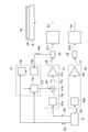
- FIG. 1 schematically illustrates a plasma processing apparatus according to one exemplary embodiment.
- FIG. 2 is a diagram illustrating an example of a configuration of a high-frequency power supply unit and an example of a configuration of a correction signal generation unit of the plasma processing apparatus illustrated in FIG. 1.
- FIG. 2 is a diagram illustrating an example of a timing chart related to generation of plasma in the plasma processing apparatus illustrated in FIG. 1.
- FIG. 2 is a diagram illustrating an example of a reflected wave monitor signal and an example of an inverted-phase signal generated in the plasma processing apparatus illustrated in FIG. 1.
- 5 is a flowchart illustrating a method for generating a plasma according to one exemplary embodiment.
- a plasma processing apparatus in one exemplary embodiment, includes a chamber, a high-frequency power supply, and a correction signal generator.
- the high-frequency power supply unit is configured to output pulsed high-frequency power or combined high-frequency power to generate plasma from gas in the chamber.
- the composite high-frequency power is a composite power of the pulsed high-frequency power and the corrected high-frequency power.
- the corrected high-frequency power is power that oscillates in the opposite phase to the reflected wave with respect to the pulsed high-frequency power.
- the correction signal generator is configured to generate a correction signal.
- the correction signal is a signal that oscillates in the opposite phase to the reflected wave monitor signal representing the reflected wave with respect to the pulsed high-frequency power.
- the high-frequency power supply unit is configured to output pulsed high-frequency power during the first period.
- the correction signal generation unit is configured to generate a correction signal from the reflected wave monitor signal in the first period.
- the high-frequency power supply unit is configured to output a composite high-frequency power generated using the correction signal in each of one or more second periods after the first period.
- the high-frequency power supply unit is configured to alternately repeat the output of the pulsed high-frequency power in the first period and the output of the combined high-frequency power in one or more second periods.
- the combined high-frequency power is output in each of the one or more second periods.
- the corrected high-frequency power included in the combined high-frequency power is generated using a correction signal that oscillates in a phase opposite to the reflected wave monitor signal. Therefore, according to the plasma processing apparatus, the reflected wave is reduced in each of the one or more second periods.
- the combined high-frequency power is generated using the correction signal in each of one or more second periods. The first period and the one or more second periods are alternately repeated. Therefore, the synthesized high-frequency power suitable for reducing the reflected wave can be updated in a timely manner.
- the plasma processing apparatus further includes a directional coupler.
- the directional coupler is provided on an electric path through which the pulsed high-frequency power and the combined high-frequency power output from the high-frequency power supply are transmitted.
- the correction signal generation unit is configured to generate a correction signal from the reflected wave monitor signal output by the directional coupler.
- the high-frequency power supply includes a high-frequency signal generator, an adder, and an amplifier.
- the high frequency signal generator is configured to generate a pulsed high frequency signal.
- the adder is configured to generate a composite high-frequency signal by adding the correction signal to the pulse-like high-frequency signal.
- the amplifier is configured to generate pulsed high-frequency power by amplifying a pulsed high-frequency signal and generate composite high-frequency power by amplifying the composite high-frequency signal. In the first period, the correction signal is not added to the pulsed high-frequency signal.
- the first period and the one or more second periods may be the same periods as a plurality of consecutive periods defined by a predetermined frequency.
- the correction signal generation unit generates an anti-phase signal of the reflected wave monitor signal, and corrects the anti-phase signal so as to eliminate the dependence of the amplification factor on the amplitude of the input signal of the amplifier.
- the amplification factor of the amplifier may have a dependency on the amplitude of the input signal, that is, an amplitude dependency of the amplification factor.
- the correction signal is generated such that the amplitude dependency of the amplification factor of the amplifier is canceled in advance.
- the plasma processing apparatus includes the high-frequency power supply unit as a first high-frequency power supply unit.
- the plasma processing apparatus further includes a support, a second high-frequency power supply, and a synchronization signal generator.
- the support has a lower electrode.
- the support is configured to support the substrate in the chamber.
- the second high-frequency power supply unit is electrically connected to the support table, and is configured to output another high-frequency power.
- the frequency of the other high frequency power is lower than the frequency of the pulsed high frequency power.
- the synchronization signal generator is configured to generate a synchronization signal synchronized with another high-frequency power.
- the first period and the one or more second periods are respectively the same as a plurality of successive periods of another high-frequency power.
- the first high-frequency power supply unit generates pulsed high-frequency power in a first period in response to a synchronization signal, and generates combined high-frequency power in each of one or more second periods in response to the synchronization signal. It is configured.
- a method for generating a plasma in a chamber of a plasma processing apparatus.
- the method includes the steps of (i) outputting a pulsed high-frequency power in a first period to generate plasma from a gas in a chamber; and (ii) a reflected wave representing a reflected wave with respect to the pulsed high-frequency power.
- the composite high-frequency power is a composite power of the pulsed high-frequency power and the corrected high-frequency power.
- the corrected high-frequency power is power that oscillates in the opposite phase to the reflected wave with respect to the pulsed high-frequency power.
- the corrected high frequency power is generated using the correction signal.
- the output of pulsed high-frequency power in the first period and the output of combined high-frequency power in one or more second periods are alternately repeated. And so on.
- FIG. 1 is a view schematically showing a plasma processing apparatus according to one exemplary embodiment.
- the plasma processing apparatus 1 shown in FIG. 1 is a capacitively coupled plasma etching apparatus.
- the plasma processing apparatus 1 includes a chamber 10.
- the chamber 10 provides an internal space 10s therein.
- the chamber 10 includes a chamber body 12.
- the chamber main body 12 has a substantially cylindrical shape.
- the internal space 10 s is provided inside the chamber main body 12.
- the chamber main body 12 is formed of, for example, aluminum.
- a film having corrosion resistance is provided on the inner wall surface of the chamber main body 12.
- the film having corrosion resistance may be a film formed from a ceramic such as aluminum oxide or yttrium oxide.
- a passage 12p is formed in the side wall of the chamber body 12.
- the substrate W passes through the passage 12p when transported between the internal space 10s and the outside of the chamber 10.
- the passage 12p can be opened and closed by a gate valve 12g.
- the gate valve 12g is provided along the side wall of the chamber main body 12.
- a support 13 is provided on the bottom of the chamber body 12.
- the support 13 is formed from an insulating material.
- the support part 13 has a substantially cylindrical shape.
- the support portion 13 extends upward from the bottom of the chamber body 12 in the internal space 10s.
- the support section 13 supports a support base 14.
- the support 14 is provided in the internal space 10s.
- the support base 14 is configured to support the substrate W in the chamber 10, that is, in the internal space 10s.
- the support 14 has a lower electrode 18 and an electrostatic chuck 20.
- the support 14 may further include an electrode plate 16.
- the electrode plate 16 is formed of a conductor such as aluminum, for example, and has a substantially disk shape.
- the lower electrode 18 is provided on the electrode plate 16.
- the lower electrode 18 is formed of a conductor such as aluminum, and has a substantially disk shape.
- the lower electrode 18 is electrically connected to the electrode plate 16.
- the electrostatic chuck 20 is provided on the lower electrode 18.
- the substrate W is placed on the upper surface of the electrostatic chuck 20.
- the electrostatic chuck 20 has a main body and an electrode.
- the main body of the electrostatic chuck 20 has a substantially disk shape and is formed of a dielectric.
- the electrode of the electrostatic chuck 20 is a film-shaped electrode, and is provided in the main body of the electrostatic chuck 20.
- the electrode of the electrostatic chuck 20 is connected to a DC power supply 20p via a switch 20s. When a voltage from the DC power supply 20p is applied to the electrodes of the electrostatic chuck 20, an electrostatic attraction is generated between the electrostatic chuck 20 and the substrate W.
- the substrate W is attracted to the electrostatic chuck 20 by the generated electrostatic attraction, and is held by the electrostatic chuck 20.
- a focus ring FR is arranged on the periphery of the lower electrode 18 so as to surround the edge of the substrate W.
- the focus ring FR is provided to improve the in-plane uniformity of the plasma processing on the substrate W.
- the focus ring FR can be formed from, but not limited to, silicon, silicon carbide, or quartz.
- a flow path 18f is provided inside the lower electrode 18.
- a heat exchange medium for example, a refrigerant
- the heat exchange medium supplied to the flow path 18f is returned to the chiller unit 22 via the pipe 22b.
- the temperature of the substrate W placed on the electrostatic chuck 20 is adjusted by heat exchange between the heat exchange medium and the lower electrode 18.
- the plasma processing apparatus 1 is provided with a gas supply line 24.
- the gas supply line 24 supplies the heat transfer gas (for example, He gas) from the heat transfer gas supply mechanism between the upper surface of the electrostatic chuck 20 and the back surface of the substrate W.
- the plasma processing apparatus 1 further includes an upper electrode 30.
- the upper electrode 30 is provided above the support base 14.
- the upper electrode 30 is supported on the upper part of the chamber main body 12 via a member 32.
- the member 32 is formed from a material having an insulating property. The upper electrode 30 and the member 32 close the upper opening of the chamber body 12.
- the upper electrode 30 may include a top plate 34 and a support 36.
- the lower surface of the top plate 34 is the lower surface on the side of the internal space 10s, and defines the internal space 10s.
- the top plate 34 may be formed of a low-resistance conductor or semiconductor having low Joule heat.
- a plurality of gas discharge holes 34a are formed in the top plate 34. The plurality of gas discharge holes 34a penetrate the top plate 34 in the plate thickness direction.
- the support 36 detachably supports the top plate 34.
- the support 36 is formed from a conductive material such as aluminum.
- a gas diffusion chamber 36 a is provided inside the support 36.
- the support 36 has a plurality of gas holes 36b.
- the plurality of gas holes 36b extend downward from the gas diffusion chamber 36a.
- the plurality of gas holes 36b communicate with the plurality of gas discharge holes 34a, respectively.
- the support 36 has a gas inlet 36c formed therein.
- the gas inlet 36c is connected to the gas diffusion chamber 36a.
- a gas supply pipe 38 is connected to the gas inlet 36c.
- a gas source group 40 is connected to the gas supply pipe 38 via a valve group 41, a flow controller group 42, and a valve group 43.
- the gas source group 40 includes a plurality of gas sources.
- Each of the valve group 41 and the valve group 43 includes a plurality of open / close valves.
- the flow controller group 42 includes a plurality of flow controllers.
- Each of the plurality of flow controllers of the flow controller group 42 is a mass flow controller or a pressure control type flow controller.
- Each of the plurality of gas sources of the gas source group 40 is connected to a gas supply pipe via a corresponding open / close valve of the valve group 41, a corresponding flow controller of the flow controller group 42, and a corresponding open / close valve of the valve group 43. 38.
- the shield 46 is provided detachably along the inner wall surface of the chamber main body 12.
- the shield 46 is also provided on the outer periphery of the support 13.
- the shield 46 prevents the etching by-product from adhering to the chamber body 12.
- the shield 46 is formed by forming a film having corrosion resistance on the surface of a member formed of, for example, aluminum.
- the corrosion resistant film may be a film formed from a ceramic such as yttrium oxide.
- a baffle plate 48 is provided between the support 13 and the side wall of the chamber body 12.
- the baffle plate 48 is formed by forming a film having corrosion resistance on the surface of a member formed of, for example, aluminum.
- the corrosion resistant film may be a film formed from a ceramic such as yttrium oxide.
- the baffle plate 48 has a plurality of through holes.
- An exhaust port 12 e is provided below the baffle plate 48 and at the bottom of the chamber body 12.
- An exhaust device 50 is connected to the exhaust port 12e via an exhaust pipe 52.
- the exhaust device 50 has a vacuum pump such as a pressure regulating valve and a turbo molecular pump.
- the plasma processing apparatus 1 further includes a high frequency power supply unit 61.
- the high-frequency power supply 61 is an example of a first high-frequency power supply.
- the high-frequency power supply 61 is configured to output high-frequency power HF in order to generate plasma from gas in the chamber 10.
- the fundamental frequency of the high-frequency power HF is, for example, a frequency in a range of 27 MHz to 100 MHz. In one example, the fundamental frequency of the high frequency power HF is 40.68 MHz.
- the high-frequency power supply 61 is electrically connected to the lower electrode 18 via the matching unit 63.
- the matching unit 63 has a matching circuit.
- the matching circuit of the matching unit 63 is configured to match the impedance on the load side (lower electrode side) of the high-frequency power supply unit 61 with the output impedance of the high-frequency power supply unit 61.
- the high-frequency power supply unit 61 may be electrically connected to the upper electrode 30 via the matching unit 63.
- the plasma processing apparatus 1 may further include a directional coupler 65.
- the directional coupler 65 is provided on the electric path EP1.
- the high frequency power HF is output by the high frequency power supply 61 and transmitted on the electric path EP1.
- the directional coupler 65 is provided between the high-frequency power supply unit 61 and the matching unit 63.
- the directional coupler 65 branches a part of the reflected wave with respect to the high-frequency power HF from the electric path EP1.
- the directional coupler 65 outputs a part of the reflected wave as a reflected wave monitor signal MS.
- the plasma processing apparatus 1 may further include a high-frequency power supply unit 62.
- the high-frequency power supply unit 62 is an example of a second high-frequency power supply unit.
- the high frequency power supply unit 62 is configured to output the high frequency power LF.
- the high-frequency power LF has a frequency suitable for mainly drawing ions into the substrate W.
- the fundamental frequency of the high-frequency power LF is, for example, a frequency in the range of 400 kHz to 13.56 MHz. In one example, the fundamental frequency of the high-frequency power LF is 400 kHz.
- the high frequency power supply unit 62 is electrically connected to the lower electrode 18 via the matching unit 64.
- the matching unit 64 has a matching circuit.
- the matching circuit of the matching unit 64 is configured to match the impedance on the load side (lower electrode side) of the high-frequency power supply unit 62 with the output impedance of the high-frequency power supply unit 62.
- the plasma processing apparatus 1 may further include a directional coupler 66.
- the directional coupler 66 is provided on the electric path EP2.
- the high-frequency power LF is output by the high-frequency power supply unit 62 and transmitted on the electric path EP2.
- the directional coupler 66 is provided between the high-frequency power supply unit 62 and the matching unit 64.
- the directional coupler 66 branches a part of the reflected wave with respect to the high-frequency power LF from the electric path EP2.
- the directional coupler 66 outputs a part of the reflected wave as a reflected wave monitor signal.
- the reflected wave monitor signal from the directional coupler 66 is used, for example, for power control of the high-frequency power LF.
- the plasma processing apparatus 1 may further include a control unit 80.
- the control unit 80 may be a computer including a processor, a storage unit such as a memory, an input device, a display device, a signal input / output interface, and the like.
- the control unit 80 controls each unit of the plasma processing apparatus 1.
- an operator can perform a command input operation or the like for managing the plasma processing apparatus 1 using the input device.
- the operation status of the plasma processing apparatus 1 can be visualized and displayed on the display device.
- a control program and recipe data are stored in the storage unit of the control unit 80.
- the control program is executed by the processor of the control unit 80 to execute various processes in the plasma processing apparatus 1.
- the processor of the control unit 80 executes the control program and controls each unit of the plasma processing apparatus 1 according to the recipe data, so that the plasma processing apparatus 1 executes a method MT described later.
- FIG. 2 is a diagram illustrating an example of a configuration of a power supply unit and an example of a configuration of a correction signal generation unit of the plasma processing apparatus illustrated in FIG.
- FIG. 3 is a diagram showing an example of a timing chart related to generation of plasma in the plasma processing apparatus shown in FIG.
- FIG. 4 is a diagram illustrating an example of a reflected wave monitor signal and an example of an inverted-phase signal generated in the plasma processing apparatus illustrated in FIG.
- the high-frequency power supply 61 is configured to output a pulsed high-frequency power PHF or a combined high-frequency power SHF as the high-frequency power HF.
- the pulsed high-frequency power PHF is high-frequency power whose power level is set such that the power level in a certain period is higher than the power levels in periods before and after the period.
- the pulsed high-frequency power PHF is set to an ON state during a certain period, and is set to an OFF state before and after the period. That is, in one example, the pulsed high-frequency power PHF has a power level for generating plasma in a certain period, and is set to 0 W before and after the period.
- the combined high-frequency power SHF is a composite power of the pulsed high-frequency power PHF and the corrected high-frequency power.
- the corrected high-frequency power is power that vibrates in a phase opposite to the reflected wave with respect to the pulsed high-frequency power PHF.
- the high-frequency power supply 61 is configured to output a pulsed high-frequency power PHF in the first period P1.
- the timing at which the output of the pulsed high-frequency power PHF is started within the first period P1 and the length of time during which the pulsed high-frequency power PHF is output within the first period P1 are determined by the control unit 80 by the high-frequency power supply unit 61. Is specified.
- the high-frequency power supply unit 61 is configured to output the combined high-frequency power SHF in each of the one or more second periods P2.
- One or more second periods P2 are periods after the first period P1.
- One or more second periods P2 may sequentially follow the first period P1.
- the time length of each of the one or more second periods P2 may be the same as the time length of the first period P1.
- the first period P1 and the one or more second periods P2 may be the same periods as a plurality of continuous periods defined by a predetermined frequency.
- the high-frequency power supply 61 is configured to alternately repeat the output of the pulsed high-frequency power PHF in the first period P1 and the output of the combined high-frequency power SHF in one or more second periods P2. Note that, in the example illustrated in FIG. 3, four second periods P2 follow the first period P1, but the number of second periods after the first period P1 is not limited. .
- the high-frequency power supply 61 is configured to generate the composite high-frequency power SHF using the correction signal CS.
- the correction signal CS is generated by the correction signal generator 70.
- the correction signal generator 70 is configured to generate a correction signal CS from the reflected wave monitor signal MS in the first period P1.
- the reflected wave monitor signal MS is output by the directional coupler 65.
- the correction signal CS is a signal that oscillates in the opposite phase to the reflected wave monitor signal MS.
- the correction signal generation unit 70 includes an A / D converter 70a, a calculator 70b, and a D / A converter 70c.
- the A / D converter 70a performs A / D conversion on the reflected wave monitor signal MS to generate a digital signal.
- the digital signal generated by the A / D converter 70a is provided to the calculator 70b as a reflected wave monitor digital signal.
- the computing unit 70b is, for example, a processor.
- the arithmetic unit 70b generates an inverted signal RS of the reflected wave monitor digital signal.
- the anti-phase signal RS is a signal that oscillates in the opposite phase to the reflected wave monitor signal MS, and the anti-phase signal RS is obtained by performing only a 180 ° phase inversion process on the reflected wave monitor signal MS. Generated.
- the correction signal CS may be an analog signal generated by D / A conversion of the negative-phase signal RS. That is, the computing unit 70b may output the inverted-phase signal RS as a correction digital signal.
- the correction signal generation unit 70 may be configured to generate a correction signal by correcting the negative-phase signal RS. Specifically, the arithmetic unit 70b corrects the amplitude of the negative-phase signal RS so as to eliminate the dependency of the amplification factor on the amplitude of the input signal of the amplifier 61c (non-linear dependency), thereby converting the corrected digital signal. May be generated.
- the correction digital signal generated by the arithmetic unit 70b is provided to the D / A converter 70c.
- the D / A converter 70c performs a D / A conversion on the input correction digital signal to generate a correction signal CS (analog signal).
- the correction signal CS generated by the D / A converter 70c is provided to the high-frequency power supply unit 61.
- the correction signal generation unit 70 does not supply the correction signal CS to the high frequency power supply unit 61 in the first period P1.
- the correction signal generation section 70 supplies the correction signal CS to the high-frequency power supply section 61 in each of one or more second periods P2 after the first period P1.
- the high-frequency power supply unit 61 includes a high-frequency signal generator 61a, an adder 61b, and an amplifier 61c.
- the high-frequency signal generator 61a is configured to generate a pulsed high-frequency signal PS.
- the high-frequency signal generator 61a is, for example, a function generator.
- the fundamental frequency of the pulsed high-frequency signal PS generated by the high-frequency signal generator 61a is the same as the fundamental frequency of the high-frequency power HF.
- the high-frequency signal generator 61a is configured to output a pulsed high-frequency signal PS in each of the first period P1 and one or more second periods P2.
- the timing at which the high-frequency signal generator 61a starts outputting the pulsed high-frequency signal PS is specified by the control unit 80 to the high-frequency signal generator 61a.
- the time length during which the high-frequency signal generator 61a outputs the pulsed high-frequency signal PS is specified by the control unit 80 to the high-frequency signal generator 61a. Is done.
- the adder 61b receives the pulsed high-frequency signal PS from the high-frequency signal generator 61a. Further, the adder 61b receives the correction signal CS from the correction signal generator 70. The adder 61b is configured to add the correction signal CS to the pulsed high-frequency signal PS and generate a composite high-frequency signal AS. When the correction signal CS is not provided, the adder 61b outputs a pulsed high-frequency signal PS.
- the amplifier 61c is configured to generate a pulsed high frequency power PHF by amplifying the pulsed high frequency signal PS. The amplifier 61c is configured to generate the combined high-frequency power SHF by amplifying the combined high-frequency signal AS.
- the high-frequency power supply unit 62 has a high-frequency signal generator 62a and an amplifier 62c.
- the high frequency signal generator 62a is configured to generate a high frequency signal.
- the high-frequency signal generator 62a is, for example, a function generator.
- the frequency of the high-frequency signal generated by the high-frequency signal generator 62a is the same as the frequency of the high-frequency power LF.
- the amplifier 62c amplifies the high-frequency signal from the high-frequency signal generator 62a to generate a high-frequency power LF.
- the high frequency signal generator 62a may generate a high frequency signal continuously. That is, the high-frequency power supply unit 62 may continuously output the high-frequency power LF.
- the high frequency signal generator 62a may generate a pulsed high frequency signal. That is, the high-frequency power supply unit 62 may output the pulsed high-frequency power LF.
- the first period P1 and the one or more second periods P2 are the same as a plurality of continuous periods of the high-frequency power LF. That is, the output of the pulsed high-frequency power PHF and the combined high-frequency power SHF is performed within the corresponding cycle of the high-frequency power LF.
- the plasma processing apparatus 1 may further include a synchronization signal generator 76.
- the synchronization signal generator 76 generates the synchronization signal SS and outputs the synchronization signal SS.
- the synchronization signal SS includes, for example, a synchronization pulse at the start of each cycle of the high-frequency power LF.
- the high-frequency power supply unit 62 outputs the high-frequency power LF so that each cycle is synchronized with the synchronization signal SS (the synchronization pulse) given from the synchronization signal generator 76.
- the synchronization signal is also supplied to the correction signal generation unit 70 and the high frequency power supply unit 61.
- the correction signal generation unit 70 sends the correction signal CS to the high-frequency power supply unit 61 at a timing specified by the delay time given from the control unit 80 with reference to the synchronization pulse of the synchronization signal SS.
- the high-frequency signal generator 61a of the high-frequency power supply unit 61 determines the timing defined by the delay time given from the control unit 80 with reference to the synchronization pulse of the synchronization signal SS in each of the first period P1 and the second period P2. Then, the output of the high frequency signal PS is started.
- the combined high-frequency power SHF is output in each of the one or more second periods P2.
- the corrected high-frequency power included in the combined high-frequency power SHF is generated using a correction signal CS that oscillates in the opposite phase to the reflected wave monitor signal MS. Therefore, according to the plasma processing apparatus 1, the reflected wave is reduced in each of the one or more second periods P2.
- the correction signal CS is generated by outputting the pulsed high-frequency power PHF in the first period P1
- the combined high-frequency power SHF is generated using the correction signal CS in each of one or more second periods. Is done.
- the first period P1 and one or more second periods P2 are alternately repeated. Therefore, the plasma processing apparatus 1 can update the combined high-frequency power SHF suitable for reducing the reflected wave in a timely manner.
- the correction signal CS is generated so that the amplitude dependency (non-linear dependency) of the amplification factor of the amplifier 61c is canceled in advance.
- the reflected wave can be further reduced.
- the correction signal CS has a delay time adjusted so as to cancel the reflected wave with respect to the pulsed high-frequency power PHF, and can be used for generating the composite high-frequency power SHF.
- the correction signal CS can be added to the pulsed high-frequency signal PS with a delay time adjusted to cancel the reflected wave for the pulsed high-frequency power PHF.
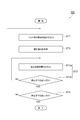
- FIG. 5 is a flowchart illustrating a method of generating a plasma according to one exemplary embodiment.
- the method MT will be described using the case where the plasma processing apparatus 1 is used as an example. However, the method MT may be performed using another plasma processing apparatus capable of performing the plurality of steps.
- Step ST1 pulsed high-frequency power PHF is output from the high-frequency power supply 61 to generate plasma from gas in the chamber 10.
- the pulsed high-frequency power PHF is output in the first period P1.
- the correction signal CS is generated by the correction signal generation unit 70.
- the correction signal CS is a signal that oscillates in the opposite phase to the reflected wave monitor signal MS.
- the reflected wave monitor signal MS is a signal representing a reflected wave with respect to the pulsed high-frequency power PHF.
- the reflected wave monitor signal MS is provided to the correction signal generator 70 by the directional coupler 65.
- Step ST3 includes step ST3a and step ST3b.
- step ST3a the combined high-frequency power SHF is output to generate plasma from gas in the chamber 10.
- the combined high-frequency power SHF is output in the second period P2.
- the composite high frequency power SHF is a composite power of the pulsed high frequency power PHF and the corrected high frequency power.
- the corrected high-frequency power is power that oscillates in the opposite phase to the reflected wave.
- the combined high-frequency power SHF is generated using the correction signal CS.
- step ST3b it is determined whether a stop condition is satisfied.
- step ST3b it is determined that the stop condition is satisfied when the number of times of execution of step ST3a has reached a predetermined number. If it is determined in step ST3b that the stop condition is not satisfied, step ST3a is executed again. On the other hand, if it is determined in step ST3b that the stop condition is satisfied, step ST4 is performed. When the predetermined number of times is 1, the step ST3b is unnecessary.
- step ST4 it is determined whether another stop condition is satisfied.
- step ST4 when the number of executions of the sequence including step ST1, step ST2, and step ST3 has reached a predetermined number, it is determined that the other stop condition is satisfied.
- the predetermined number is a plurality of times. If it is determined in step ST4 that the other stop condition is not satisfied, the above sequence is executed again. On the other hand, when it is determined in step ST4 that the other stop condition is satisfied, the method MT ends.
- the step ST1 is executed, so that the pulsed high-frequency power PHF is output in the first period P1.
- the combined high-frequency power SHF is output in each of one or more second periods P2 after the first period P1.
- the process ST1 and the process ST3 are such that the output of the pulsed high-frequency power in the first period P1 and the output of the combined high-frequency power in one or more second periods P2 are alternately repeated. Be executed.
- the high-frequency power LF may be supplied.
- each of the first period P1 and the one or more second periods P2 may be synchronized with a corresponding cycle of the high-frequency power LF.
- the plasma processing apparatus may include only a single high-frequency power supply unit that outputs pulsed high-frequency power, similarly to the high-frequency power supply unit 61.
- the fundamental frequency of the high-frequency power output from the single high-frequency power supply unit may be any frequency as long as plasma can be generated.
- the plasma processing apparatus may be an inductively coupled plasma processing apparatus.
- the high-frequency power supply unit 61 may be electrically connected to an antenna.
- the antenna creates a magnetic field in the chamber for generating a plasma.
- An antenna may be provided on the top of the chamber.
- the high frequency power supply unit 61 and the high frequency power supply unit 62 may be connected to the lower electrode, and another high frequency power supply may be connected to the antenna.
- a plasma processing apparatus may be a plasma processing apparatus that uses microwaves to generate plasma. Microwaves can be introduced from an antenna provided on the top of the chamber.
- the high frequency power supply 61 and the high frequency power supply 62 are connected to the lower electrode.
- the combined high-frequency power SHF is generated by amplifying the combined high-frequency signal AS by the amplifier 61c.
- the correction RF signal may be generated by amplifying the correction signal CS by another amplifier.
- the combined high-frequency power SHF is generated by adding the corrected high-frequency power to the pulsed high-frequency power PHF at the subsequent stage of the amplifier 61c.
Landscapes
- Engineering & Computer Science (AREA)
- Physics & Mathematics (AREA)
- Chemical & Material Sciences (AREA)
- Plasma & Fusion (AREA)
- Analytical Chemistry (AREA)
- Mechanical Engineering (AREA)
- Condensed Matter Physics & Semiconductors (AREA)
- Microelectronics & Electronic Packaging (AREA)
- Power Engineering (AREA)
- Computer Hardware Design (AREA)
- Organic Chemistry (AREA)
- Manufacturing & Machinery (AREA)
- General Chemical & Material Sciences (AREA)
- Chemical Kinetics & Catalysis (AREA)
- Materials Engineering (AREA)
- General Physics & Mathematics (AREA)
- Metallurgy (AREA)
- Spectroscopy & Molecular Physics (AREA)
- Electromagnetism (AREA)
- Plasma Technology (AREA)
- Chemical Vapour Deposition (AREA)
- Drying Of Semiconductors (AREA)
- Treatment Of Fiber Materials (AREA)
Priority Applications (3)
| Application Number | Priority Date | Filing Date | Title |
|---|---|---|---|
| CN201980004388.3A CN111052874B (zh) | 2018-06-22 | 2019-06-10 | 等离子体处理装置和生成等离子体的方法 |
| KR1020207006605A KR102723098B1 (ko) | 2018-06-22 | 2019-06-10 | 플라즈마 처리 장치 및 플라즈마를 생성하는 방법 |
| US16/645,188 US10978274B2 (en) | 2018-06-22 | 2019-06-10 | Plasma processing apparatus and method for generating plasma |
Applications Claiming Priority (2)
| Application Number | Priority Date | Filing Date | Title |
|---|---|---|---|
| JP2018119084A JP6842443B2 (ja) | 2018-06-22 | 2018-06-22 | プラズマ処理装置及びプラズマを生成する方法 |
| JP2018-119084 | 2018-06-22 |
Publications (1)
| Publication Number | Publication Date |
|---|---|
| WO2019244698A1 true WO2019244698A1 (ja) | 2019-12-26 |
Family
ID=68983385
Family Applications (1)
| Application Number | Title | Priority Date | Filing Date |
|---|---|---|---|
| PCT/JP2019/022954 Ceased WO2019244698A1 (ja) | 2018-06-22 | 2019-06-10 | プラズマ処理装置及びプラズマを生成する方法 |
Country Status (6)
| Country | Link |
|---|---|
| US (1) | US10978274B2 (enExample) |
| JP (1) | JP6842443B2 (enExample) |
| KR (1) | KR102723098B1 (enExample) |
| CN (1) | CN111052874B (enExample) |
| TW (1) | TWI812738B (enExample) |
| WO (1) | WO2019244698A1 (enExample) |
Cited By (15)
| Publication number | Priority date | Publication date | Assignee | Title |
|---|---|---|---|---|
| US11476145B2 (en) | 2018-11-20 | 2022-10-18 | Applied Materials, Inc. | Automatic ESC bias compensation when using pulsed DC bias |
| US11699572B2 (en) | 2019-01-22 | 2023-07-11 | Applied Materials, Inc. | Feedback loop for controlling a pulsed voltage waveform |
| US11791138B2 (en) | 2021-05-12 | 2023-10-17 | Applied Materials, Inc. | Automatic electrostatic chuck bias compensation during plasma processing |
| US11798790B2 (en) | 2020-11-16 | 2023-10-24 | Applied Materials, Inc. | Apparatus and methods for controlling ion energy distribution |
| US11848176B2 (en) | 2020-07-31 | 2023-12-19 | Applied Materials, Inc. | Plasma processing using pulsed-voltage and radio-frequency power |
| US11887813B2 (en) | 2021-06-23 | 2024-01-30 | Applied Materials, Inc. | Pulsed voltage source for plasma processing |
| US11901157B2 (en) | 2020-11-16 | 2024-02-13 | Applied Materials, Inc. | Apparatus and methods for controlling ion energy distribution |
| US11948780B2 (en) | 2021-05-12 | 2024-04-02 | Applied Materials, Inc. | Automatic electrostatic chuck bias compensation during plasma processing |
| US11967483B2 (en) | 2021-06-02 | 2024-04-23 | Applied Materials, Inc. | Plasma excitation with ion energy control |
| US11972924B2 (en) | 2022-06-08 | 2024-04-30 | Applied Materials, Inc. | Pulsed voltage source for plasma processing applications |
| US12106938B2 (en) | 2021-09-14 | 2024-10-01 | Applied Materials, Inc. | Distortion current mitigation in a radio frequency plasma processing chamber |
| US12198966B2 (en) | 2017-09-20 | 2025-01-14 | Applied Materials, Inc. | Substrate support with multiple embedded electrodes |
| US12261019B2 (en) | 2021-08-24 | 2025-03-25 | Applied Materials, Inc. | Voltage pulse time-domain multiplexing |
| US12272524B2 (en) | 2022-09-19 | 2025-04-08 | Applied Materials, Inc. | Wideband variable impedance load for high volume manufacturing qualification and on-site diagnostics |
| US12315732B2 (en) | 2022-06-10 | 2025-05-27 | Applied Materials, Inc. | Method and apparatus for etching a semiconductor substrate in a plasma etch chamber |
Families Citing this family (12)
| Publication number | Priority date | Publication date | Assignee | Title |
|---|---|---|---|---|
| US11508554B2 (en) | 2019-01-24 | 2022-11-22 | Applied Materials, Inc. | High voltage filter assembly |
| KR102593142B1 (ko) * | 2020-05-19 | 2023-10-25 | 세메스 주식회사 | 기판 처리 장치 및 그의 페라이트 코어 온도 제어 방법 |
| KR20230073145A (ko) | 2020-09-29 | 2023-05-25 | 램 리써치 코포레이션 | Rf 생성기들의 동기화 |
| US11495470B1 (en) | 2021-04-16 | 2022-11-08 | Applied Materials, Inc. | Method of enhancing etching selectivity using a pulsed plasma |
| US20220399185A1 (en) | 2021-06-09 | 2022-12-15 | Applied Materials, Inc. | Plasma chamber and chamber component cleaning methods |
| US12148595B2 (en) | 2021-06-09 | 2024-11-19 | Applied Materials, Inc. | Plasma uniformity control in pulsed DC plasma chamber |
| US11810760B2 (en) | 2021-06-16 | 2023-11-07 | Applied Materials, Inc. | Apparatus and method of ion current compensation |
| US11776788B2 (en) | 2021-06-28 | 2023-10-03 | Applied Materials, Inc. | Pulsed voltage boost for substrate processing |
| US11694876B2 (en) * | 2021-12-08 | 2023-07-04 | Applied Materials, Inc. | Apparatus and method for delivering a plurality of waveform signals during plasma processing |
| US11990319B2 (en) * | 2022-01-05 | 2024-05-21 | Applied Materials, Inc. | Methods and apparatus for processing a substrate |
| US12111341B2 (en) | 2022-10-05 | 2024-10-08 | Applied Materials, Inc. | In-situ electric field detection method and apparatus |
| JP2024062195A (ja) * | 2022-10-24 | 2024-05-09 | 東京エレクトロン株式会社 | 周波数可変電源及びプラズマ処理装置 |
Citations (4)
| Publication number | Priority date | Publication date | Assignee | Title |
|---|---|---|---|---|
| JP2000049000A (ja) * | 1998-07-31 | 2000-02-18 | Kem Kk | 周波数整合器 |
| JP2012174736A (ja) * | 2011-02-17 | 2012-09-10 | Mitsubishi Electric Corp | プラズマ成膜装置及びプラズマ成膜方法 |
| WO2017062083A1 (en) * | 2015-10-05 | 2017-04-13 | Applied Materials, Inc. | Rf power delivery regulation for processing substrates |
| JP2017228558A (ja) * | 2016-06-20 | 2017-12-28 | 東京エレクトロン株式会社 | プラズマ処理装置、及び波形補正方法 |
Family Cites Families (23)
| Publication number | Priority date | Publication date | Assignee | Title |
|---|---|---|---|---|
| KR100525961B1 (ko) | 1996-11-04 | 2005-12-21 | 어플라이드 머티어리얼스, 인코포레이티드 | 플라즈마시스에서발생하는고주파를필터링하는플라즈마처리장치및방법 |
| JP3629705B2 (ja) | 1997-06-06 | 2005-03-16 | 東京エレクトロン株式会社 | プラズマ処理装置 |
| JP3027572B1 (ja) * | 1998-12-24 | 2000-04-04 | 日本高周波株式会社 | プラズマ処理用インピーダンス測定装置 |
| KR100807724B1 (ko) * | 2003-08-07 | 2008-02-28 | 가부시키가이샤 히다치 고쿠사이 덴키 | 기판처리장치 및 기판처리방법 |
| JP3998630B2 (ja) * | 2003-11-19 | 2007-10-31 | 株式会社東芝 | 電力増幅器 |
| JP4879548B2 (ja) * | 2005-09-30 | 2012-02-22 | 株式会社ダイヘン | 高周波電源装置 |
| JP2007134849A (ja) * | 2005-11-09 | 2007-05-31 | Nagano Japan Radio Co | 増幅装置 |
| JP5210659B2 (ja) * | 2008-02-28 | 2013-06-12 | 株式会社日立ハイテクノロジーズ | プラズマ処理装置 |
| JP5319150B2 (ja) * | 2008-03-31 | 2013-10-16 | 東京エレクトロン株式会社 | プラズマ処理装置及びプラズマ処理方法及びコンピュータ読み取り可能な記憶媒体 |
| JP4891384B2 (ja) * | 2009-12-10 | 2012-03-07 | 株式会社新川 | プラズマ発生装置 |
| JP2012174668A (ja) * | 2011-02-24 | 2012-09-10 | Mitsubishi Electric Corp | 高周波電力供給装置、プラズマ処理装置、及び半導体薄膜の製造方法 |
| JP5867701B2 (ja) * | 2011-12-15 | 2016-02-24 | 東京エレクトロン株式会社 | プラズマ処理装置 |
| JP5808012B2 (ja) * | 2011-12-27 | 2015-11-10 | 東京エレクトロン株式会社 | プラズマ処理装置 |
| US9462672B2 (en) * | 2012-02-22 | 2016-10-04 | Lam Research Corporation | Adjustment of power and frequency based on three or more states |
| US9171700B2 (en) * | 2012-06-15 | 2015-10-27 | COMET Technologies USA, Inc. | Plasma pulse tracking system and method |
| JP6202644B2 (ja) * | 2013-08-26 | 2017-09-27 | 株式会社日立国際電気 | プラズマ生成用電源装置 |
| JP6512962B2 (ja) * | 2014-09-17 | 2019-05-15 | 東京エレクトロン株式会社 | プラズマ処理装置 |
| KR101677748B1 (ko) * | 2014-10-29 | 2016-11-29 | 삼성전자 주식회사 | 펄스 플라즈마 장치 및 펄스 플라즈마 장치 구동 방법 |
| CN105826154B (zh) | 2015-01-06 | 2017-12-19 | 北京北方华创微电子装备有限公司 | 针对脉冲射频电源的阻抗匹配方法及装置 |
| JP6396822B2 (ja) * | 2015-02-16 | 2018-09-26 | 東京エレクトロン株式会社 | プラズマ処理装置のサセプタの電位を制御する方法 |
| KR102260998B1 (ko) * | 2016-08-25 | 2021-06-04 | 한국전기연구원 | 펄스 전원 보상 장치 및 이를 포함하는 고전압 펄스 전원 시스템 |
| WO2018061617A1 (ja) * | 2016-09-28 | 2018-04-05 | 株式会社日立国際電気 | 高周波電源装置 |
| US10546724B2 (en) * | 2017-05-10 | 2020-01-28 | Mks Instruments, Inc. | Pulsed, bidirectional radio frequency source/load |
-
2018
- 2018-06-22 JP JP2018119084A patent/JP6842443B2/ja active Active
-
2019
- 2019-06-10 KR KR1020207006605A patent/KR102723098B1/ko active Active
- 2019-06-10 CN CN201980004388.3A patent/CN111052874B/zh active Active
- 2019-06-10 WO PCT/JP2019/022954 patent/WO2019244698A1/ja not_active Ceased
- 2019-06-10 US US16/645,188 patent/US10978274B2/en active Active
- 2019-06-18 TW TW108120965A patent/TWI812738B/zh active
Patent Citations (4)
| Publication number | Priority date | Publication date | Assignee | Title |
|---|---|---|---|---|
| JP2000049000A (ja) * | 1998-07-31 | 2000-02-18 | Kem Kk | 周波数整合器 |
| JP2012174736A (ja) * | 2011-02-17 | 2012-09-10 | Mitsubishi Electric Corp | プラズマ成膜装置及びプラズマ成膜方法 |
| WO2017062083A1 (en) * | 2015-10-05 | 2017-04-13 | Applied Materials, Inc. | Rf power delivery regulation for processing substrates |
| JP2017228558A (ja) * | 2016-06-20 | 2017-12-28 | 東京エレクトロン株式会社 | プラズマ処理装置、及び波形補正方法 |
Cited By (21)
| Publication number | Priority date | Publication date | Assignee | Title |
|---|---|---|---|---|
| US12198966B2 (en) | 2017-09-20 | 2025-01-14 | Applied Materials, Inc. | Substrate support with multiple embedded electrodes |
| US11476145B2 (en) | 2018-11-20 | 2022-10-18 | Applied Materials, Inc. | Automatic ESC bias compensation when using pulsed DC bias |
| US12057292B2 (en) | 2019-01-22 | 2024-08-06 | Applied Materials, Inc. | Feedback loop for controlling a pulsed voltage waveform |
| US11699572B2 (en) | 2019-01-22 | 2023-07-11 | Applied Materials, Inc. | Feedback loop for controlling a pulsed voltage waveform |
| US12237148B2 (en) | 2020-07-31 | 2025-02-25 | Applied Materials, Inc. | Plasma processing assembly using pulsed-voltage and radio-frequency power |
| US11848176B2 (en) | 2020-07-31 | 2023-12-19 | Applied Materials, Inc. | Plasma processing using pulsed-voltage and radio-frequency power |
| US11901157B2 (en) | 2020-11-16 | 2024-02-13 | Applied Materials, Inc. | Apparatus and methods for controlling ion energy distribution |
| US12183557B2 (en) | 2020-11-16 | 2024-12-31 | Applied Materials, Inc. | Apparatus and methods for controlling ion energy distribution |
| US11798790B2 (en) | 2020-11-16 | 2023-10-24 | Applied Materials, Inc. | Apparatus and methods for controlling ion energy distribution |
| US11948780B2 (en) | 2021-05-12 | 2024-04-02 | Applied Materials, Inc. | Automatic electrostatic chuck bias compensation during plasma processing |
| US11791138B2 (en) | 2021-05-12 | 2023-10-17 | Applied Materials, Inc. | Automatic electrostatic chuck bias compensation during plasma processing |
| US12347647B2 (en) | 2021-06-02 | 2025-07-01 | Applied Materials, Inc. | Plasma excitation with ion energy control |
| US11967483B2 (en) | 2021-06-02 | 2024-04-23 | Applied Materials, Inc. | Plasma excitation with ion energy control |
| US11887813B2 (en) | 2021-06-23 | 2024-01-30 | Applied Materials, Inc. | Pulsed voltage source for plasma processing |
| US12125673B2 (en) | 2021-06-23 | 2024-10-22 | Applied Materials, Inc. | Pulsed voltage source for plasma processing applications |
| US12261019B2 (en) | 2021-08-24 | 2025-03-25 | Applied Materials, Inc. | Voltage pulse time-domain multiplexing |
| US12106938B2 (en) | 2021-09-14 | 2024-10-01 | Applied Materials, Inc. | Distortion current mitigation in a radio frequency plasma processing chamber |
| US11972924B2 (en) | 2022-06-08 | 2024-04-30 | Applied Materials, Inc. | Pulsed voltage source for plasma processing applications |
| US12368020B2 (en) | 2022-06-08 | 2025-07-22 | Applied Materials, Inc. | Pulsed voltage source for plasma processing applications |
| US12315732B2 (en) | 2022-06-10 | 2025-05-27 | Applied Materials, Inc. | Method and apparatus for etching a semiconductor substrate in a plasma etch chamber |
| US12272524B2 (en) | 2022-09-19 | 2025-04-08 | Applied Materials, Inc. | Wideband variable impedance load for high volume manufacturing qualification and on-site diagnostics |
Also Published As
| Publication number | Publication date |
|---|---|
| US10978274B2 (en) | 2021-04-13 |
| CN111052874A (zh) | 2020-04-21 |
| TW202002727A (zh) | 2020-01-01 |
| US20200286714A1 (en) | 2020-09-10 |
| KR102723098B1 (ko) | 2024-10-28 |
| JP6842443B2 (ja) | 2021-03-17 |
| TWI812738B (zh) | 2023-08-21 |
| JP2019220435A (ja) | 2019-12-26 |
| CN111052874B (zh) | 2023-02-28 |
| KR20210021441A (ko) | 2021-02-26 |
Similar Documents
| Publication | Publication Date | Title |
|---|---|---|
| JP6842443B2 (ja) | プラズマ処理装置及びプラズマを生成する方法 | |
| CN113451101B (zh) | 等离子体处理方法和等离子体处理装置 | |
| JP7374362B2 (ja) | プラズマ処理方法及びプラズマ処理装置 | |
| JP2020004710A (ja) | 制御方法及びプラズマ処理装置 | |
| CN111524782A (zh) | 等离子体处理装置 | |
| JP6762410B2 (ja) | プラズマ処理装置及び制御方法 | |
| JP2020109838A (ja) | プラズマ処理装置及び制御方法 | |
| CN111524781B (zh) | 高频电源及等离子体处理装置 | |
| JP7395645B2 (ja) | プラズマ処理装置 | |
| JP2017228558A (ja) | プラズマ処理装置、及び波形補正方法 | |
| JP2020205361A (ja) | プラズマ処理方法及びプラズマ処理装置 | |
| JP6180890B2 (ja) | プラズマ処理方法 | |
| TWI828773B (zh) | 電漿處理方法及電漿處理裝置 | |
| TW201335992A (zh) | 電漿處理方法及電漿處理裝置 | |
| JP6960421B2 (ja) | プラズマ処理装置及びプラズマ処理方法 | |
| JPH01236629A (ja) | プラズマ処理装置 | |
| CN121148980A (zh) | 等离子体处理方法及等离子体处理装置 |
Legal Events
| Date | Code | Title | Description |
|---|---|---|---|
| 121 | Ep: the epo has been informed by wipo that ep was designated in this application |
Ref document number: 19822705 Country of ref document: EP Kind code of ref document: A1 |
|
| NENP | Non-entry into the national phase |
Ref country code: DE |
|
| 122 | Ep: pct application non-entry in european phase |
Ref document number: 19822705 Country of ref document: EP Kind code of ref document: A1 |