WO2019230668A1 - 半導体装置製造方法 - Google Patents
半導体装置製造方法 Download PDFInfo
- Publication number
- WO2019230668A1 WO2019230668A1 PCT/JP2019/020955 JP2019020955W WO2019230668A1 WO 2019230668 A1 WO2019230668 A1 WO 2019230668A1 JP 2019020955 W JP2019020955 W JP 2019020955W WO 2019230668 A1 WO2019230668 A1 WO 2019230668A1
- Authority
- WO
- WIPO (PCT)
- Prior art keywords
- wafer
- group
- cleaning process
- semiconductor device
- adhesive layer
- Prior art date
- Legal status (The legal status is an assumption and is not a legal conclusion. Google has not performed a legal analysis and makes no representation as to the accuracy of the status listed.)
- Ceased
Links
Images



Classifications
-
- H—ELECTRICITY
- H10—SEMICONDUCTOR DEVICES; ELECTRIC SOLID-STATE DEVICES NOT OTHERWISE PROVIDED FOR
- H10W—GENERIC PACKAGES, INTERCONNECTIONS, CONNECTORS OR OTHER CONSTRUCTIONAL DETAILS OF DEVICES COVERED BY CLASS H10
- H10W20/00—Interconnections in chips, wafers or substrates
- H10W20/01—Manufacture or treatment
- H10W20/021—Manufacture or treatment of interconnections within wafers or substrates
- H10W20/023—Manufacture or treatment of interconnections within wafers or substrates the interconnections being through-semiconductor vias
-
- C—CHEMISTRY; METALLURGY
- C09—DYES; PAINTS; POLISHES; NATURAL RESINS; ADHESIVES; COMPOSITIONS NOT OTHERWISE PROVIDED FOR; APPLICATIONS OF MATERIALS NOT OTHERWISE PROVIDED FOR
- C09J—ADHESIVES; NON-MECHANICAL ASPECTS OF ADHESIVE PROCESSES IN GENERAL; ADHESIVE PROCESSES NOT PROVIDED FOR ELSEWHERE; USE OF MATERIALS AS ADHESIVES
- C09J183/00—Adhesives based on macromolecular compounds obtained by reactions forming in the main chain of the macromolecule a linkage containing silicon, with or without sulfur, nitrogen, oxygen, or carbon only; Adhesives based on derivatives of such polymers
- C09J183/04—Polysiloxanes
- C09J183/06—Polysiloxanes containing silicon bound to oxygen-containing groups
-
- H—ELECTRICITY
- H10—SEMICONDUCTOR DEVICES; ELECTRIC SOLID-STATE DEVICES NOT OTHERWISE PROVIDED FOR
- H10P—GENERIC PROCESSES OR APPARATUS FOR THE MANUFACTURE OR TREATMENT OF DEVICES COVERED BY CLASS H10
- H10P14/00—Formation of materials, e.g. in the shape of layers or pillars
- H10P14/60—Formation of materials, e.g. in the shape of layers or pillars of insulating materials
- H10P14/63—Formation of materials, e.g. in the shape of layers or pillars of insulating materials characterised by the formation processes
- H10P14/6326—Deposition processes
- H10P14/6342—Liquid deposition, e.g. spin-coating, sol-gel techniques or spray coating
-
- H—ELECTRICITY
- H10—SEMICONDUCTOR DEVICES; ELECTRIC SOLID-STATE DEVICES NOT OTHERWISE PROVIDED FOR
- H10P—GENERIC PROCESSES OR APPARATUS FOR THE MANUFACTURE OR TREATMENT OF DEVICES COVERED BY CLASS H10
- H10P14/00—Formation of materials, e.g. in the shape of layers or pillars
- H10P14/60—Formation of materials, e.g. in the shape of layers or pillars of insulating materials
- H10P14/69—Inorganic materials
- H10P14/692—Inorganic materials composed of oxides, glassy oxides or oxide-based glasses
- H10P14/6921—Inorganic materials composed of oxides, glassy oxides or oxide-based glasses containing silicon
- H10P14/6922—Inorganic materials composed of oxides, glassy oxides or oxide-based glasses containing silicon the material containing Si, O and at least one of H, N, C, F or other non-metal elements, e.g. SiOC, SiOC:H or SiONC
-
- H—ELECTRICITY
- H10—SEMICONDUCTOR DEVICES; ELECTRIC SOLID-STATE DEVICES NOT OTHERWISE PROVIDED FOR
- H10P—GENERIC PROCESSES OR APPARATUS FOR THE MANUFACTURE OR TREATMENT OF DEVICES COVERED BY CLASS H10
- H10P50/00—Etching of wafers, substrates or parts of devices
- H10P50/69—Etching of wafers, substrates or parts of devices using masks for semiconductor materials
- H10P50/691—Etching of wafers, substrates or parts of devices using masks for semiconductor materials for Group V materials or Group III-V materials
-
- H—ELECTRICITY
- H10—SEMICONDUCTOR DEVICES; ELECTRIC SOLID-STATE DEVICES NOT OTHERWISE PROVIDED FOR
- H10P—GENERIC PROCESSES OR APPARATUS FOR THE MANUFACTURE OR TREATMENT OF DEVICES COVERED BY CLASS H10
- H10P70/00—Cleaning of wafers, substrates or parts of devices
- H10P70/20—Cleaning during device manufacture
- H10P70/23—Cleaning during device manufacture during, before or after processing of insulating materials
- H10P70/234—Cleaning during device manufacture during, before or after processing of insulating materials the processing being the formation of vias or contact holes
-
- H—ELECTRICITY
- H10—SEMICONDUCTOR DEVICES; ELECTRIC SOLID-STATE DEVICES NOT OTHERWISE PROVIDED FOR
- H10W—GENERIC PACKAGES, INTERCONNECTIONS, CONNECTORS OR OTHER CONSTRUCTIONAL DETAILS OF DEVICES COVERED BY CLASS H10
- H10W20/00—Interconnections in chips, wafers or substrates
- H10W20/01—Manufacture or treatment
- H10W20/021—Manufacture or treatment of interconnections within wafers or substrates
- H10W20/023—Manufacture or treatment of interconnections within wafers or substrates the interconnections being through-semiconductor vias
- H10W20/0234—Manufacture or treatment of interconnections within wafers or substrates the interconnections being through-semiconductor vias comprising etching via holes that stop on pads or on electrodes
-
- H—ELECTRICITY
- H10—SEMICONDUCTOR DEVICES; ELECTRIC SOLID-STATE DEVICES NOT OTHERWISE PROVIDED FOR
- H10W—GENERIC PACKAGES, INTERCONNECTIONS, CONNECTORS OR OTHER CONSTRUCTIONAL DETAILS OF DEVICES COVERED BY CLASS H10
- H10W20/00—Interconnections in chips, wafers or substrates
- H10W20/01—Manufacture or treatment
- H10W20/021—Manufacture or treatment of interconnections within wafers or substrates
- H10W20/023—Manufacture or treatment of interconnections within wafers or substrates the interconnections being through-semiconductor vias
- H10W20/0242—Manufacture or treatment of interconnections within wafers or substrates the interconnections being through-semiconductor vias comprising etching via holes from the back sides of the chips, wafers or substrates
-
- H—ELECTRICITY
- H10—SEMICONDUCTOR DEVICES; ELECTRIC SOLID-STATE DEVICES NOT OTHERWISE PROVIDED FOR
- H10W—GENERIC PACKAGES, INTERCONNECTIONS, CONNECTORS OR OTHER CONSTRUCTIONAL DETAILS OF DEVICES COVERED BY CLASS H10
- H10W20/00—Interconnections in chips, wafers or substrates
- H10W20/01—Manufacture or treatment
- H10W20/021—Manufacture or treatment of interconnections within wafers or substrates
- H10W20/023—Manufacture or treatment of interconnections within wafers or substrates the interconnections being through-semiconductor vias
- H10W20/0253—Manufacture or treatment of interconnections within wafers or substrates the interconnections being through-semiconductor vias comprising forming the through-semiconductor vias after stacking of the chips, wafers or substrates
-
- H—ELECTRICITY
- H10—SEMICONDUCTOR DEVICES; ELECTRIC SOLID-STATE DEVICES NOT OTHERWISE PROVIDED FOR
- H10W—GENERIC PACKAGES, INTERCONNECTIONS, CONNECTORS OR OTHER CONSTRUCTIONAL DETAILS OF DEVICES COVERED BY CLASS H10
- H10W20/00—Interconnections in chips, wafers or substrates
- H10W20/01—Manufacture or treatment
- H10W20/071—Manufacture or treatment of dielectric parts thereof
- H10W20/074—Manufacture or treatment of dielectric parts thereof of dielectric parts comprising thin functional dielectric layers, e.g. dielectric etch-stop, barrier, capping or liner layers
- H10W20/076—Manufacture or treatment of dielectric parts thereof of dielectric parts comprising thin functional dielectric layers, e.g. dielectric etch-stop, barrier, capping or liner layers in via holes or trenches
-
- H—ELECTRICITY
- H10—SEMICONDUCTOR DEVICES; ELECTRIC SOLID-STATE DEVICES NOT OTHERWISE PROVIDED FOR
- H10W—GENERIC PACKAGES, INTERCONNECTIONS, CONNECTORS OR OTHER CONSTRUCTIONAL DETAILS OF DEVICES COVERED BY CLASS H10
- H10W20/00—Interconnections in chips, wafers or substrates
- H10W20/20—Interconnections within wafers or substrates, e.g. through-silicon vias [TSV]
-
- H—ELECTRICITY
- H10—SEMICONDUCTOR DEVICES; ELECTRIC SOLID-STATE DEVICES NOT OTHERWISE PROVIDED FOR
- H10W—GENERIC PACKAGES, INTERCONNECTIONS, CONNECTORS OR OTHER CONSTRUCTIONAL DETAILS OF DEVICES COVERED BY CLASS H10
- H10W20/00—Interconnections in chips, wafers or substrates
- H10W20/20—Interconnections within wafers or substrates, e.g. through-silicon vias [TSV]
- H10W20/211—Through-semiconductor vias, e.g. TSVs
- H10W20/213—Cross-sectional shapes or dispositions
- H10W20/2134—TSVs extending from the semiconductor wafer into back-end-of-line layers
-
- H—ELECTRICITY
- H10—SEMICONDUCTOR DEVICES; ELECTRIC SOLID-STATE DEVICES NOT OTHERWISE PROVIDED FOR
- H10W—GENERIC PACKAGES, INTERCONNECTIONS, CONNECTORS OR OTHER CONSTRUCTIONAL DETAILS OF DEVICES COVERED BY CLASS H10
- H10W72/00—Interconnections or connectors in packages
-
- H—ELECTRICITY
- H10—SEMICONDUCTOR DEVICES; ELECTRIC SOLID-STATE DEVICES NOT OTHERWISE PROVIDED FOR
- H10W—GENERIC PACKAGES, INTERCONNECTIONS, CONNECTORS OR OTHER CONSTRUCTIONAL DETAILS OF DEVICES COVERED BY CLASS H10
- H10W90/00—Package configurations
-
- C—CHEMISTRY; METALLURGY
- C08—ORGANIC MACROMOLECULAR COMPOUNDS; THEIR PREPARATION OR CHEMICAL WORKING-UP; COMPOSITIONS BASED THEREON
- C08G—MACROMOLECULAR COMPOUNDS OBTAINED OTHERWISE THAN BY REACTIONS ONLY INVOLVING UNSATURATED CARBON-TO-CARBON BONDS
- C08G77/00—Macromolecular compounds obtained by reactions forming a linkage containing silicon with or without sulfur, nitrogen, oxygen or carbon in the main chain of the macromolecule
- C08G77/04—Polysiloxanes
- C08G77/14—Polysiloxanes containing silicon bound to oxygen-containing groups
-
- H—ELECTRICITY
- H10—SEMICONDUCTOR DEVICES; ELECTRIC SOLID-STATE DEVICES NOT OTHERWISE PROVIDED FOR
- H10W—GENERIC PACKAGES, INTERCONNECTIONS, CONNECTORS OR OTHER CONSTRUCTIONAL DETAILS OF DEVICES COVERED BY CLASS H10
- H10W72/00—Interconnections or connectors in packages
- H10W72/01—Manufacture or treatment
- H10W72/013—Manufacture or treatment of die-attach connectors
- H10W72/01331—Manufacture or treatment of die-attach connectors using blanket deposition
- H10W72/01333—Manufacture or treatment of die-attach connectors using blanket deposition in liquid form, e.g. spin coating, spray coating or immersion coating
-
- H—ELECTRICITY
- H10—SEMICONDUCTOR DEVICES; ELECTRIC SOLID-STATE DEVICES NOT OTHERWISE PROVIDED FOR
- H10W—GENERIC PACKAGES, INTERCONNECTIONS, CONNECTORS OR OTHER CONSTRUCTIONAL DETAILS OF DEVICES COVERED BY CLASS H10
- H10W72/00—Interconnections or connectors in packages
- H10W72/01—Manufacture or treatment
- H10W72/0198—Manufacture or treatment batch processes
-
- H—ELECTRICITY
- H10—SEMICONDUCTOR DEVICES; ELECTRIC SOLID-STATE DEVICES NOT OTHERWISE PROVIDED FOR
- H10W—GENERIC PACKAGES, INTERCONNECTIONS, CONNECTORS OR OTHER CONSTRUCTIONAL DETAILS OF DEVICES COVERED BY CLASS H10
- H10W72/00—Interconnections or connectors in packages
- H10W72/071—Connecting or disconnecting
- H10W72/073—Connecting or disconnecting of die-attach connectors
- H10W72/07331—Connecting techniques
- H10W72/07332—Compression bonding, e.g. thermocompression bonding
-
- H—ELECTRICITY
- H10—SEMICONDUCTOR DEVICES; ELECTRIC SOLID-STATE DEVICES NOT OTHERWISE PROVIDED FOR
- H10W—GENERIC PACKAGES, INTERCONNECTIONS, CONNECTORS OR OTHER CONSTRUCTIONAL DETAILS OF DEVICES COVERED BY CLASS H10
- H10W72/00—Interconnections or connectors in packages
- H10W72/071—Connecting or disconnecting
- H10W72/073—Connecting or disconnecting of die-attach connectors
- H10W72/07331—Connecting techniques
- H10W72/07337—Connecting techniques using a polymer adhesive, e.g. an adhesive based on silicone or epoxy
- H10W72/07338—Connecting techniques using a polymer adhesive, e.g. an adhesive based on silicone or epoxy hardening the adhesive by curing, e.g. thermosetting
-
- H—ELECTRICITY
- H10—SEMICONDUCTOR DEVICES; ELECTRIC SOLID-STATE DEVICES NOT OTHERWISE PROVIDED FOR
- H10W—GENERIC PACKAGES, INTERCONNECTIONS, CONNECTORS OR OTHER CONSTRUCTIONAL DETAILS OF DEVICES COVERED BY CLASS H10
- H10W72/00—Interconnections or connectors in packages
- H10W72/071—Connecting or disconnecting
- H10W72/073—Connecting or disconnecting of die-attach connectors
- H10W72/07341—Controlling the bonding environment, e.g. atmosphere composition or temperature
-
- H—ELECTRICITY
- H10—SEMICONDUCTOR DEVICES; ELECTRIC SOLID-STATE DEVICES NOT OTHERWISE PROVIDED FOR
- H10W—GENERIC PACKAGES, INTERCONNECTIONS, CONNECTORS OR OTHER CONSTRUCTIONAL DETAILS OF DEVICES COVERED BY CLASS H10
- H10W72/00—Interconnections or connectors in packages
- H10W72/30—Die-attach connectors
- H10W72/351—Materials of die-attach connectors
- H10W72/353—Materials of die-attach connectors not comprising solid metals or solid metalloids, e.g. ceramics
- H10W72/354—Materials of die-attach connectors not comprising solid metals or solid metalloids, e.g. ceramics comprising polymers
-
- H—ELECTRICITY
- H10—SEMICONDUCTOR DEVICES; ELECTRIC SOLID-STATE DEVICES NOT OTHERWISE PROVIDED FOR
- H10W—GENERIC PACKAGES, INTERCONNECTIONS, CONNECTORS OR OTHER CONSTRUCTIONAL DETAILS OF DEVICES COVERED BY CLASS H10
- H10W90/00—Package configurations
- H10W90/701—Package configurations characterised by the relative positions of pads or connectors relative to package parts
- H10W90/731—Package configurations characterised by the relative positions of pads or connectors relative to package parts of die-attach connectors
- H10W90/732—Package configurations characterised by the relative positions of pads or connectors relative to package parts of die-attach connectors between stacked chips
-
- H—ELECTRICITY
- H10—SEMICONDUCTOR DEVICES; ELECTRIC SOLID-STATE DEVICES NOT OTHERWISE PROVIDED FOR
- H10W—GENERIC PACKAGES, INTERCONNECTIONS, CONNECTORS OR OTHER CONSTRUCTIONAL DETAILS OF DEVICES COVERED BY CLASS H10
- H10W90/00—Package configurations
- H10W90/701—Package configurations characterised by the relative positions of pads or connectors relative to package parts
- H10W90/791—Package configurations characterised by the relative positions of pads or connectors relative to package parts of direct-bonded pads
- H10W90/792—Package configurations characterised by the relative positions of pads or connectors relative to package parts of direct-bonded pads between multiple chips
Definitions
- the present invention relates to a method for manufacturing a semiconductor device having a stacked structure including a plurality of semiconductor elements.
- a via that penetrates through a wafer that is, a through electrode, is formed to electrically connect semiconductor elements formed on different wafers in the wafer stack.
- the through electrode is formed, for example, through a process of forming a hole penetrating the wafer in the thickness direction by reactive ion etching and a process of filling the hole with a conductive material.
- an adhesive for joining wafers to be multilayered.
- a through electrode that is electrically connected to the semiconductor element of the lower wafer on the upper wafer laminated via the adhesive layer on the wafer, in the hole forming process, the upper wafer and the adhesive layer directly below the upper wafer It is necessary to form a hole by reactive ion etching so as to penetrate the hole.
- Such holes are filled with a conductive material.
- the present invention has been conceived under the circumstances as described above, and an object of the present invention is to provide a semiconductor device manufacturing method in which semiconductor elements are multilayered through lamination of semiconductor wafers via an adhesive layer. Another object of the present invention is to provide a technique suitable for realizing a low wiring resistance between semiconductor elements to be multilayered.
- the semiconductor device manufacturing method provided by the present invention is a method in which semiconductor elements are multi-layered through lamination of semiconductor wafers via an adhesive layer, and includes at least the following first to sixth steps.
- a wafer stack is prepared.
- the wafer laminate includes a first wafer having a circuit forming surface including a wiring pattern and a back surface opposite to the first wafer, a second wafer having a main surface and a back surface opposite to the main surface, and a SiOC-based polymer. And an adhesive layer interposed between the circuit forming surface of the first wafer and the back surface of the second wafer.
- the SiOC polymer is a polymer containing at least silicon, oxygen, and carbon as constituent elements, and further includes a SiOCH polymer containing hydrogen.
- the carbon ratio is, for example, 20 to 70 mass%
- the hydrogen ratio is, for example, 2 to 20 mass%
- the oxygen ratio is, for example, 10 to 40 mass%
- the silicon ratio is, for example, 3 to 40 mass%. %.
- the circuit formation surface is a surface on the side where a semiconductor element is formed on a wafer and a so-called rewiring layer is formed on the element.
- the main surface is a surface on the side where a semiconductor element is formed on the wafer.
- the second wafer and the adhesive layer are penetrated by an etching process from the second wafer side through a mask pattern that masks a part of the main surface side of the second wafer. Then, a hole reaching the wiring pattern in the first wafer is formed. In the etching process, reactive ion etching is preferably performed. Further, the portion of the wiring pattern that faces the hole forms the bottom surface of the hole.
- an insulating film is formed on the inner surface including the wall surface and bottom surface of the hole.
- a portion on the wiring pattern in the insulating film in the hole is removed by etching.
- the wafer stack in which the holes are formed is subjected to a cleaning process.
- This cleaning process includes an oxygen plasma cleaning process and / or an argon sputtering cleaning process.
- the conductive portion is formed by filling the hole with the conductive material after the cleaning step.
- the formed conductive portion is structurally and electrically connected to the wiring pattern on the circuit forming surface of the first wafer.
- this conductive portion forms a through electrode for electrically connecting the semiconductor element derived from the first wafer and the semiconductor element derived from the second wafer.
- a barrier layer is formed on the hole wall surface before the sixth step.
- the conductive material filling method in the sixth step is preferably an electroplating method.
- the conductive portion that forms the through electrode for electrically connecting the semiconductor elements has a structure with respect to the wiring pattern on the circuit forming surface of the first wafer. Connected electrically and electrically.
- a bumpless structure is suitable for realizing a short conductive path between multilayered semiconductor elements.
- a bump electrode that is electrically connected to a through electrode that penetrates a wafer is formed on the surface of the wafer, and then electrical connection between semiconductor elements in different wafers is performed via the bump electrode. May be planned.
- the conductive portion that will form the through electrode is directly connected to the wiring pattern on the first wafer, and electrical connection between semiconductor elements on different wafers.
- a bumpless structure is formed.
- such a bumpless structure is suitable for realizing a short conductive path between semiconductor elements to be multilayered. The shorter the conductive path between semiconductor elements to be multilayered, the smaller the conductive path between the elements or the resistance of the wiring.
- the semiconductor device manufacturing method of the present invention is a method in which semiconductor elements are multi-layered through lamination of semiconductor wafers via an adhesive layer as described above, and an adhesive layer that joins the wafers. Contains a SiOC-based polymer.
- the present invention has obtained the knowledge that these configurations are suitable for realizing a low contact resistance between the conductive portion or through electrode formed in the hole and the wiring pattern on the first wafer circuit formation surface. . For example, the following examples and comparative examples are shown.
- the resistance of the entire conductive path or the entire wiring tends to be small.
- this method for manufacturing a semiconductor device is suitable for realizing a low wiring resistance between semiconductor elements that are joined together via an adhesive layer to be multilayered.
- Such a semiconductor device manufacturing method is suitable for suppressing high-speed signal transmission with low power consumption in a manufactured semiconductor device, and is preferable for suppressing attenuation of a high-frequency signal.
- the processing time is preferably 5 to 120 seconds, more preferably 10 to 60 seconds, and more preferably 15 to 40 seconds.
- the treatment time is preferably 0.5 to 5 minutes, more preferably 2 to 4 minutes.
- the cleaning process in the fifth step preferably includes an oxygen plasma cleaning process and an argon sputtering cleaning process after that.
- the washing treatment preferably includes a sulfuric acid washing treatment between these treatments.
- the adhesive layer preferably contains a siloxane-based organic-inorganic hybrid adhesive, more preferably an adhesive containing a polyorganosilsesquioxane containing a polymerizable functional group (polymerizable group-containing polyorganosilsesquioxane). It is a cured product of the composition.
- the siloxane-based organic-inorganic hybrid adhesive refers to an adhesive polymer material having a siloxane bond and including a structural unit in which an organic group is bonded to silicon forming the siloxane bond. Such an adhesive layer is suitable for achieving high heat resistance and reducing the curing temperature for forming the adhesive layer to suppress damage to elements in the wafer as an adherend.
- the thickness of the adhesive layer is preferably 5 ⁇ m or less. Such a configuration is suitable for shortening the conductive portion or the through electrode formed in the present method, and accordingly, the entire conductive path or the entire wiring between the semiconductor elements electrically connected through the through electrode. Suitable for reducing the resistance. Further, the adhesive layer containing the siloxane-based organic-inorganic hybrid adhesive is suitable for exhibiting sufficient wafer bonding strength even when it is as thin as this.
- the thickness of the second wafer is preferably 20 ⁇ m or less, more preferably 15 ⁇ m or less. Such a configuration is suitable for shortening the conductive portion or the through electrode formed in the present method, and accordingly, the entire conductive path or the entire wiring between the semiconductor elements electrically connected through the through electrode. Suitable for reducing the resistance.
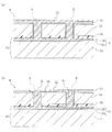
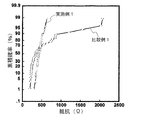
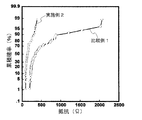
- 4 illustrates some steps in a method for manufacturing a semiconductor device according to an embodiment of the present invention. 4 illustrates some steps in a method for manufacturing a semiconductor device according to an embodiment of the present invention. 4 illustrates some steps in a method for manufacturing a semiconductor device according to an embodiment of the present invention. It is a graph showing each chain resistance measurement result which concerns on Example 1 and Comparative Example 1. FIG. It is a graph showing each chain resistance measurement result which concerns on Example 2 and Comparative Example 1.
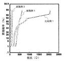
- FIG. 6 is a graph showing results of measuring chain resistance according to Examples 1 and 3 and Comparative Example 1.
- 4 is a graph showing measurement results of chain resistances according to Examples 3 and 4 and Comparative Example 1.
- FIGS. 1 to 3 show a semiconductor device manufacturing method according to an embodiment of the present invention.
- This manufacturing method is a method for manufacturing a semiconductor device having a three-dimensional structure in which semiconductor elements are integrated in the thickness direction.
- FIGS. 1 to 3 show the manufacturing process in partial cross-sectional views.
- a wafer stack W as shown in FIG. 1A is prepared (preparation process).
- the wafer laminate W has a laminated structure including the wafer 10, the wafer 20, and the adhesive layer 30 therebetween.
- the wafer 10 is a wafer that has undergone a transistor forming process and a rewiring layer forming process, and includes a main body portion 11 and a rewiring layer 12, and a circuit forming surface 10a on the rewiring layer 12 side and a back surface 10b opposite to the circuit forming surface 10a.
- a plurality of semiconductor elements (not shown) are formed on one side of the main body 11 of the wafer 10, and the rewiring layer 12 is formed on the elements.
- the rewiring layer 12 includes an insulating portion 12a and a wiring pattern 12b.
- the circuit forming surface 10a is the surface on the side where such a rewiring layer 12 is formed on the wafer 10.
- the wiring pattern 12b of the rewiring layer 12 has a portion facing the outside of the rewiring layer 12 on the circuit forming surface 10a. That is, the circuit formation surface 10a includes the exposed area of the wiring pattern 12b.
- the thickness of such a wafer 10 is, for example, 300 to 800 ⁇ m.
- the wafer 10 may be thinned later by grinding from the back surface 10b side.
- the wafer 20 is a wafer that has undergone a transistor forming process, and has a main surface 20a and a back surface 20b opposite to the main surface 20a.
- the main surface 20 a of the wafer 20 is a surface on the side where a plurality of semiconductor elements (not shown) are formed in the wafer 20.
- the thickness of the wafer 20 is 30 ⁇ m or less, preferably 20 ⁇ m or less, and more preferably 15 ⁇ m or less.
- Examples of semiconductor materials for forming the main bodies of the wafers 10 and 20 include silicon (Si), germanium (Ge), silicon carbide (SiC), gallium arsenide (GaAs), gallium nitride (GaN), and indium phosphide. (InP).
- the adhesive layer 30 contains a SiOC polymer and is interposed between the circuit forming surface 10 a of the wafer 10 and the back surface 20 b of the wafer 20.
- the SiOC polymer is a polymer containing at least silicon, oxygen, and carbon as constituent elements, and further includes a SiOCH polymer containing hydrogen.
- the carbon ratio is, for example, 20 to 70 mass%
- the hydrogen ratio is, for example, 2 to 20 mass%
- the oxygen ratio is, for example, 10 to 40 mass%
- the silicon ratio is, for example, 3 to 40 mass%. %.
- the adhesive layer 30 preferably contains a siloxane-based organic-inorganic hybrid adhesive, and more preferably is a cured product of an adhesive composition containing a polymerizable group-containing silsesquioxane.
- the siloxane-based organic-inorganic hybrid adhesive refers to an adhesive polymer material having a siloxane bond and including a structural unit in which an organic group is bonded to silicon forming the siloxane bond.
- the wafer stack W shown in FIG. 1A can be manufactured through the following processes, for example.
- a grinding process is performed on the surface of the additional wafer opposite to the wafer 10 bonding surface by using a grinding apparatus, and the additional wafer is thinned to a predetermined thickness.
- a semiconductor element is formed on the exposed surface (surface opposite to the wafer 10 bonding surface) of the thinned additional wafer through a transistor formation process and the like.
- the above-described wafer laminated body W having a laminated structure including the wafers 10 and 20 and the adhesive layer 30 bonding them can be manufactured.
- the composition for forming the above-mentioned adhesive layer 30 contains a SiOC-based material that will form the above-mentioned SiOC-based polymer as a curable resin. Such a configuration is preferable for realizing high heat resistance of the adhesive layer 30.
- the SiOC-based material is preferably a siloxane-based organic-inorganic hybrid adhesive.
- Examples of the main component of the siloxane-based organic-inorganic hybrid adhesive include polymerizable group-containing polyorganosilsesquioxane and benzocyclobutene (BCB) resin.
- the polymerizable functional group of the polymerizable group-containing polyorganosilsesquioxane is preferably an epoxy group or a (meth) acryloyloxy group.
- BCB resin examples include 1,3-divinyl-1,1,3,3-tetramethyldisiloxane-benzocyclobutene.
- CYCLOTEN manufactured by Dow Chemical Co., Ltd. can be used.
- the content ratio of the polymerizable group-containing polyorganosilsesquioxane in the composition is, for example, 70. It is at least mass%, preferably 80 to 99.8 mass%, more preferably 90 to 99.5 mass%.
- the polymerizable group-containing polyorganosilsesquioxane is contained in the composition for forming the adhesive layer 30, the polymerizable group-containing polyorganosilsesquioxane is, in this embodiment, as a siloxane constituent unit as described below.
- the structural unit [RSiO 3/2 ] is a T3 body and the structural unit [RSiO 2/2 (OR ′)] is a T2 body.
- the silicon atom is bonded to three oxygen atoms, each of which is also bonded to a silicon atom in another siloxane structural unit.
- the silicon atom is bonded to two oxygen atoms, each of which is also bonded to the silicon atom in the other siloxane structural unit, and bonded to the oxygen of the alkoxy group.
- T3 and T2 bodies are both formed by hydrolysis of a silane compound having three hydrolyzable functional groups and subsequent condensation reaction, as described above. This is a partial structure of a polymerizable group-containing polyorganosilsesquioxane.
- R 1 R 1 and in Formula (2) in the formula (1) each represent a group containing an epoxy group or (meth) acryloyloxy group.
- R 2 in the formula (2) represents a hydrogen atom or an alkyl group having 1 to 4 carbon atoms.
- each R 1 in the formula (1) and the formula (2) is an epoxy group-containing group
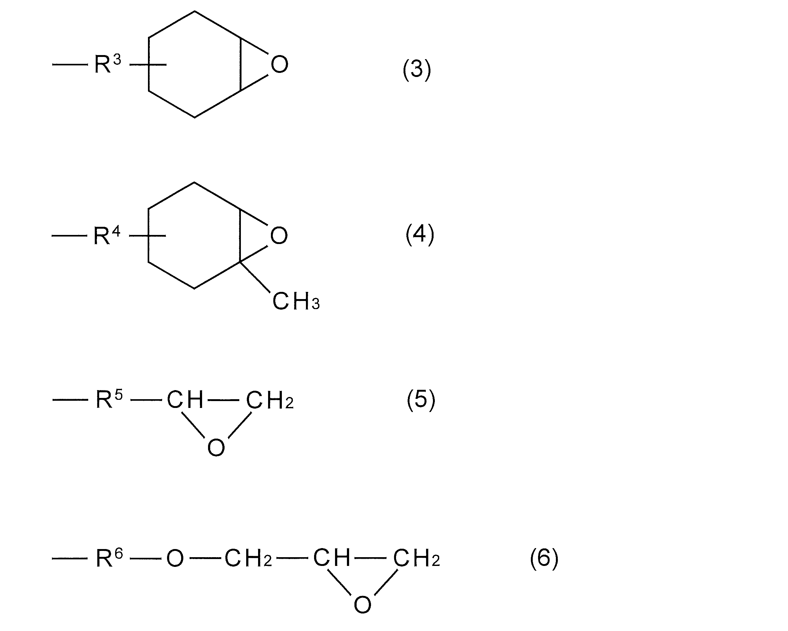
- examples of the R 1 include groups represented by the following formulas (3) to (6).
- Each of R 3 , R 4 , R 5 , and R 6 in formulas (3) to (6) represents a linear or branched alkylene group having, for example, 1 to 10 carbon atoms. Examples of such an alkylene group include a methylene group, a methylmethylene group, a dimethylmethylene group, an ethylene group, a propylene group, a trimethylene group, a tetramethylene group, a pentamethylene group, a hexamethylene group, and a decamethylene group.
- R 1 as epoxy group-containing group in the formula (1)
- R 2 in the above formula (2) represents a hydrogen atom or an alkyl group having 1 to 4 carbon atoms. Therefore, OR 2 in the formula (2) represents a hydroxy group or 1 to 4 carbon atoms. Represents an alkoxy group. Examples of the alkoxy group having 1 to 4 carbon atoms include a methoxy group, an ethoxy group, a propoxy group, an isopropoxy group, a butoxy group, and an isobutyloxy group.
- the polymerizable group-containing polyorganosilsesquioxane contained in the composition for forming the adhesive layer 30 may include one type or two or more types as the structural unit represented by the above formula (1). It may be a thing.
- the polymerizable group-containing polyorganosilsesquioxane may include one type or two or more types as a structural unit represented by the above formula (2).
- R 7 in formula (7) is a hydrogen atom, a substituted or unsubstituted alkyl group, a substituted or unsubstituted alkenyl group, a substituted or unsubstituted cycloalkyl group, a substituted or unsubstituted aryl group, or substituted or unsubstituted Represents a substituted aralkyl group.
- R 7 in Formula (7) is preferably a substituted or unsubstituted alkyl group, a substituted or unsubstituted alkenyl group, or a substituted or unsubstituted aryl group, more preferably a phenyl group.
- Examples of the alkyl group described above for R 7 include a methyl group, an ethyl group, a propyl group, an n-butyl group, an isopropyl group, an isobutyl group, an s-butyl group, a t-butyl group, and an isopentyl group.
- Examples of the alkenyl group described above for R 7 include a vinyl group, an allyl group, and an isopropenyl group.
- Examples of the cycloalkyl group described above for R 7 include a cyclobutyl group, a cyclopentyl group, and a cyclohexyl group.
- Examples of the aryl group described above with respect to R 7 include a phenyl group, a tolyl group, and a naphthyl group.
- Examples of the aralkyl group described above for R 7 include a benzyl group and a phenethyl group.
- Examples of the substituent for the alkyl group, alkenyl group, cycloalkyl group, aryl group, and aralkyl group described above for R 7 include, for example, an ether group, an ester group, a carbonyl group, a siloxane group, a fluorine atom, a halogen atom, an acrylic group, A methacryl group, a mercapto group, an amino group, and a hydroxyl group are mentioned.
- the above-mentioned polymerizable group-containing polyorganosilsesquioxane contained in the composition for forming the adhesive layer 30 includes the following formula (8): ) May be included.
- R 7 in formula (8) is a hydrogen atom, a substituted or unsubstituted alkyl group, a substituted or unsubstituted alkenyl group, a substituted or unsubstituted cycloalkyl group, a substituted or unsubstituted aryl group, or substituted or unsubstituted Represents a substituted aralkyl group, specifically the same as R 7 in the above formula (7).
- R 2 in the formula (8) represents a hydrogen atom or an alkyl group having 1 to 4 carbon atoms, and is specifically the same as R 2 in the above formula (2).
- the polymerizable group-containing polyorganosilsesquioxane has a so-called M unit [RSiO 1/2 ], in addition to the above-described first and second structural units that are T units, It may include at least one selected from the group consisting of a structural unit [R 2 SiO 2/2 ] which is a so-called D unit and a structural unit [SiO 4/2 ] which is a so-called Q unit.
- the polymerizable group-containing polyorganosilsesquioxane may have any silsesquioxane structure of cage type, incomplete cage type, ladder type, or random type, and two or more of these silsesquioxane structures are included. May have a combined structure.
- the value of the molar ratio of T3 to T2 is, for example, 5
- the lower limit is preferably 10.
- the upper limit is preferably 100, more preferably 50.
- the value of [T3 / T2] of the polyorganosilsesquioxane containing a polymerizable group is 5 to 500.
- the presence of T2 in the T3 is relatively small, and silanol hydrolysis / It means that the condensation reaction is more advanced.
- the molar ratio (T3 / T2) in the polymerizable group-containing polyorganosilsesquioxane can be determined, for example, by 29 Si-NMR spectrum measurement.
- the silicon atom in the first structural unit (T3 form) and the silicon atom in the second structural unit (T2 form) show different chemical shift peaks or signals. From the area ratio of these peaks, the value of the molar ratio can be determined.
- the 29 Si-NMR spectrum of the polymerizable group-containing polyorganosilsesquioxane can be measured, for example, with the following apparatus and conditions.
- Measuring apparatus Trade name “JNM-ECA500NMR” (manufactured by JEOL Ltd.) Solvent: Accumulated number of deuterated chloroform: 1800 times Measurement temperature: 25 ° C
- the number average molecular weight (Mn) of the polymerizable group-containing polyorganosilsesquioxane contained in the composition for forming the adhesive layer 30 is preferably 1000 to 50000, more preferably 1500 to 10,000, and still more preferably 2000 to 8000, particularly preferably 2000 to 7000.
- the number average molecular weight is 1000 or more, the insulation, heat resistance, crack resistance, and adhesiveness of the cured product formed are improved.
- the number average molecular weight is 50000 or less, the compatibility with other components in the composition is improved, and the insulation, heat resistance, and crack resistance of the cured product are improved.
- the molecular weight dispersity (Mw / Mn) of the polymerizable group-containing polyorganosilsesquioxane contained in the composition for forming the adhesive layer 30 is preferably 1.0 to 4.0, more preferably 1. It is 1 to 3.0, more preferably 1.2 to 2.7.
- Mw / Mn The molecular weight dispersity of the polymerizable group-containing polyorganosilsesquioxane contained in the composition for forming the adhesive layer 30 is preferably 1.0 to 4.0, more preferably 1. It is 1 to 3.0, more preferably 1.2 to 2.7.
- the molecular weight dispersity is 1.0 or more, the composition tends to be liquid and the handleability tends to be improved.
- the number average molecular weight (Mn) and the weight average molecular weight (Mw) of the polymerizable group-containing polyorganosilsesquioxane are measured by gel permeation chromatography (GPC) and calculated as polystyrene.
- the number average molecular weight (Mn) and the weight average molecular weight (Mw) of the polymerizable group-containing polyorganosilsesquioxane are described below using, for example, an HPLC apparatus (trade name “LC-20AD”, manufactured by Shimadzu Corporation). It can be measured according to the conditions.
- the polymerizable group-containing polyorganosilsesquioxane as described above can be produced by hydrolysis of a silane compound having three hydrolyzable functional groups and subsequent condensation reaction.
- the raw material used for the production includes at least a compound represented by the following formula (9), and optionally includes a compound represented by the following formula (10).
- the compound represented by the formula (9) is for forming the structural unit represented by the above formula (1) and the structural unit represented by the above formula (2).
- the compound represented by the formula (10) is for forming the structural unit represented by the above formula (7) and the structural unit represented by the above formula (8).
- R 1 in the formula (9) represents a group containing a polymerizable group, and is specifically the same as R 1 in the above formulas (1) and (2).
- X 1 in Formula (9) represents an alkoxy group or a halogen atom.
- the alkoxy group include an alkoxy group having 1 to 4 carbon atoms such as a methoxy group, an ethoxy group, a propoxy group, an isopropyloxy group, a butoxy group, and an isobutyloxy group.
- the halogen atom as X 1 include a fluorine atom, a chlorine atom, a bromine atom, and an iodine atom.
- X 1 is preferably an alkoxy group, more preferably a methoxy group or an ethoxy group. In the formula (9), the three X 1 may be the same or different from each other.
- R 7 in formula (10) is a substituted or unsubstituted aryl group, a substituted or unsubstituted aralkyl group, a substituted or unsubstituted cycloalkyl group, a substituted or unsubstituted alkyl group, or a substituted or unsubstituted alkenyl Represents a group, specifically the same as R 7 in the above formulas (7) and (8).
- X 2 in formula (10) represents an alkoxy group or a halogen atom, and is specifically the same as X 1 in formula (9).
- the raw material used for the production of the above-mentioned polymerizable group-containing polyorganosilsesquioxane may further contain another hydrolyzable silane compound.
- hydrolyzable trifunctional silane compounds other than both compounds represented by the above formulas (9) and (10) hydrolyzable monofunctional silane compounds that form M units
- D hydrolyzable bifunctional silane compounds that form units and hydrolyzable tetrafunctional silane compounds that form Q units.
- the amount and composition of the hydrolyzable silane compound as the raw material are appropriately adjusted according to the structure of the polymerizable group-containing polyorganosilsesquioxane that is the production target.
- the amount of the compound represented by the formula (9) used is, for example, 55 to 100 mol%, preferably 65 to 100 mol%, based on the total amount of the hydrolyzable silane compound used.
- the amount of the compound represented by the above formula (10) is, for example, 0 to 70 mol% with respect to the total amount of the hydrolyzable silane compound to be used.
- the total amount of the compound represented by the formula (9) and the compound represented by the formula (10) based on the total amount of the hydrolyzable silane compound to be used is, for example, 60 to 100 mol%, preferably 70 to 100 mol%. More preferably, it is 80 to 100 mol%.
- hydrolysis and condensation reaction for each type of hydrolyzable silane compound can be performed simultaneously. Can also be performed sequentially.
- the above hydrolysis and condensation reaction is preferably performed in the presence of one kind or two or more kinds of solvents.
- the solvent include ethers such as diethyl ether, dimethoxyethane, tetrahydrofuran, and dioxane, and ketones such as acetone, methyl ethyl ketone, and methyl isobutyl ketone.
- the usage-amount of a solvent is suitably adjusted according to reaction time etc. within the range of 2000 mass parts or less per 100 mass parts of hydrolysable silane compounds, for example.
- the above hydrolysis and condensation reaction preferably proceeds in the presence of one or more catalysts and water.
- the catalyst may be an acid catalyst or an alkali catalyst.
- the amount of the catalyst used is appropriately adjusted within a range of, for example, 0.002 to 0.2 mol per mol of the hydrolyzable silane compound.
- the amount of water used is appropriately adjusted within a range of, for example, 0.5 to 20 mol per mol of the hydrolyzable silane compound.
- the hydrolysis and condensation reaction of the hydrolyzable silane compound may be performed in one stage or may be performed in two or more stages.
- the reaction temperature of the first stage hydrolysis and condensation reaction is: For example, it is 40 to 100 ° C., preferably 45 to 80 ° C.
- the reaction time for the first stage hydrolysis and condensation reaction is, for example, 0.1 to 10 hours, preferably 1.5 to 8 hours.
- the reaction temperature of the second stage hydrolysis and condensation reaction is preferably 5 to 200 ° C., more preferably 30 to 100 ° C.
- the reaction time for the hydrolysis and condensation reaction in the second stage is not particularly limited, but is preferably 0.5 to 1000 hours, more preferably 1 to 500 hours.
- the hydrolysis and condensation reaction described above can be performed under normal pressure, under pressure, or under reduced pressure.
- the hydrolysis and condensation reaction described above is preferably performed in an atmosphere of an inert gas such as nitrogen or argon.
- the above-mentioned polymerizable group-containing polyorganosilsesquioxane is obtained by hydrolysis and condensation reaction of the hydrolyzable silane compound as described above. After completion of the reaction, the catalyst is preferably neutralized to suppress ring opening of the polymerizable group.
- the polymerizable group-containing polyorganosilsesquioxane thus obtained is purified as necessary.
- composition for forming the adhesive layer 30 preferably contains at least one curing catalyst in addition to the polymerizable group-containing polyorganosilsesquioxane produced as described above, for example.
- Examples of the curing catalyst in the case where the composition for forming the adhesive layer 30 includes an epoxy group-containing polyorganosilsesquioxane include a thermal cationic polymerization initiator.
- Examples of the curing catalyst when the composition for forming the adhesive layer 30 includes a (meth) acryloyloxy group-containing polyorganosilsesquioxane include a thermal radical polymerization initiator.
- the content of the curing catalyst in the composition for forming the adhesive layer 30 is preferably 0.1 to 3.0 parts by mass per 100 parts by mass of the polymerizable group-containing polyorganosilsesquioxane.
- thermal cationic polymerization initiator examples include thermal cationic polymerization initiators of the type such as arylsulfonium salts, aluminum chelates, and boron trifluoride amine complexes.
- arylsulfonium salts include hexafluoroantimonate salts.
- aluminum chelate examples include ethyl acetoacetate aluminum diisopropylate and aluminum tris (ethyl acetoacetate).
- boron trifluoride amine complex examples include boron trifluoride monoethylamine complex, boron trifluoride imidazole complex, and boron trifluoride piperidine complex.
- thermal radical polymerization initiator examples include thermal radical polymerization initiators of a type such as azo compounds and peroxides.
- azo compound for example, 2,2′-azobisisobutyronitrile, 2,2′-azobis (2,4-dimethylvaleronitrile), 2,2′-azobis (4-methoxy-2,4- Dimethylvaleronitrile), dimethyl-2,2'-azobis (2-methylpropionate), 2,2'-azobis (isobutyric acid) dimethyl, diethyl-2,2'-azobis (2-methylpropionate) And dibutyl-2,2′-azobis (2-methylpropionate).
- azo compound for example, 2,2′-azobisisobutyronitrile, 2,2′-azobis (2,4-dimethylvaleronitrile), 2,2′-azobis (4-methoxy-2,4- Dimethylvaleronitrile), dimethyl-2,2'-azobis (2-methylpropionate), 2,2'-azobis (iso
- peroxides examples include benzoyl peroxide, t-butylperoxy-2-ethylhexanoate, 2,5-dimethyl-2,5-di (2-ethylhexanoyl) peroxyhexane, and t-butyl.
- Peroxybenzoate t-butyl peroxide, cumene hydroperoxide, dicumyl peroxide, di-t-butyl peroxide, 2,5-dimethyl-2,5-dibutylperoxyhexane, 2,4-dichlorobenzoyl peroxide Oxide, 1,4-di (2-t-butylperoxyisopropyl) benzene, 1,1-bis (t-butylperoxy) -3,3,5-trimethylcyclohexane, methyl ethyl ketone peroxide, and 1,1, 3,3-tetramethylbutylperoxy-2-ethylhexanoate is mentioned.
- the composition for forming the adhesive layer 30 may include one or more other curable compounds in addition to the above-described polymerizable group-containing polyorganosilsesquioxane.
- the curable compound include epoxy compounds other than the above-described polymerizable group-containing polyorganosilsesquioxane, (meth) acryloyloxy group-containing compounds, vinyl group-containing compounds, oxetane compounds, and vinyl ether compounds.
- Examples of the epoxy compound other than the above-mentioned polymerizable group-containing polyorganosilsesquioxane include, for example, an alicyclic epoxy compound (alicyclic epoxy resin), an aromatic epoxy compound (aromatic epoxy resin), and an aliphatic epoxy compound. (Aliphatic epoxy resin).
- Examples of the alicyclic epoxy compound include 3,4,3 ′, 4′-diepoxybicyclohexane, 2,2-bis (3,4-epoxycyclohexyl) propane, and 1,2-bis (3,4- 1, epoxycyclohexyl) ethane, 2,3-bis (3,4-epoxycyclohexyl) oxirane, bis (3,4-epoxycyclohexylmethyl) ether, and 1,2-bis (hydroxymethyl) -1-butanol 2-epoxy-4- (2-oxiranyl) cyclohexane adduct (for example, trade name “EHPE3150” of Daicel Corporation) may be mentioned.
- aromatic epoxy compounds examples include epibis type glycidyl ether type epoxy resins and novolak alkyl type glycidyl ether type epoxy resins.
- Examples of the aliphatic epoxy compound include a glycidyl ether of q-valent alcohol (q is a natural number) having no cyclic structure, a glycidyl ester of a monovalent carboxylic acid or a polyvalent carboxylic acid, and a double bond.
- Examples include epoxidized oils and fats.
- Examples of epoxidized oils and fats having double bonds include epoxidized linseed oil, epoxidized soybean oil, and epoxidized castor oil.
- Examples of the (meth) acryloyloxy group-containing compound include trimethylolpropane tri (meth) acrylate, ditrimethylolpropane tetra (meth) acrylate, pentaerythritol tri (meth) acrylate, pentaerythritol tetra (meth) acrylate, Pentaerythritol penta (meth) acrylate, dipentaerythritol hexa (meth) acrylate, glycerol tri (meth) acrylate, tris (2-hydroxyethyl) isocyanurate tri (meth) acrylate, ethylene glycol di (meth) acrylate, 1,3 -Butanediol di (meth) acrylate, 1,4-butanediol di (meth) acrylate, 1,6-hexanediol di (meth) acrylate, neopentyl glycol di
- Examples of the above-mentioned vinyl group-containing compound include styrene and divinylbenzene.
- oxetane compound examples include 3,3-bis (vinyloxymethyl) oxetane, 3-ethyl-3- (hydroxymethyl) oxetane, 3-ethyl-3- (2-ethylhexyloxymethyl) oxetane, 3- Ethyl-3- (hydroxymethyl) oxetane, 3-ethyl-3-[(phenoxy) methyl] oxetane, 3-ethyl-3- (hexyloxymethyl) oxetane, 3-ethyl-3- (chloromethyl) oxetane, and 3,3-bis (chloromethyl) oxetane.
- Examples of the above-mentioned vinyl ether compounds include 2-hydroxyethyl vinyl ether, 3-hydroxypropyl vinyl ether, 2-hydroxypropyl vinyl ether, 2-hydroxyisopropyl vinyl ether, 4-hydroxybutyl vinyl ether, 3-hydroxybutyl vinyl ether, 2-hydroxybutyl vinyl ether.
- the composition for forming the adhesive layer 30 preferably contains a solvent in order to adjust its coatability and the like.
- the solvent include propylene glycol monomethyl ether acetate, methyl ethyl ketone, methyl isobutyl ketone, cyclohexanone, toluene, xylene, ethyl acetate, butyl acetate, 3-methoxybutyl acetate, methoxypropyl acetate, ethylene glycol monomethyl ether acetate, methanol, ethanol,
- Examples include isopropyl alcohol, 1-butanol, 1-methoxy-2-propanol, 3-methoxybutanol, ethoxyethanol, diisopropyl ether, ethylene glycol dimethyl ether, and tetrahydrofuran.
- the composition for forming the adhesive layer 30 further includes a silane coupling agent, an antifoaming agent, an antioxidant, an antiblocking agent, a leveling agent, a surfactant, an extender, an antirust agent, an antistatic agent, a plasticizer, and the like. Various additives may be included.
- the carbon ratio is preferably 20 to 70 mass%, more preferably 30 to 70 mass%, more preferably 40 to 60 mass%
- the hydrogen ratio is Preferably it is 2 to 20% by mass, more preferably 3 to 15% by mass, more preferably 4 to 10% by mass
- the oxygen ratio is preferably 10 to 40% by mass, more preferably 15 to 35% by mass, more
- the amount is preferably 20 to 30% by mass
- the silicon ratio is preferably 3 to 40% by mass, more preferably 5 to 30% by mass, and more preferably 10 to 20% by mass.
- Such a configuration is sufficient to achieve high heat resistance in the formed adhesive layer 30 and to suppress shrinkage at the time of curing, while setting the thickness of the formed adhesive layer 30 to, for example, 5 ⁇ m or less. It is suitable for developing a high wafer bonding strength.
- Each element ratio can be identified by, for example, CHN elemental analysis, Si quantitative analysis (gravimetric method), ICP emission analysis, X-ray photoelectron spectroscopic analysis, or the like.
- the composition for forming the adhesive layer 30 is spin-coated on the surface of one of the wafers to be bonded. It is applied to form an adhesive composition layer, and the composition layer is dried by heating and solidified. The heating temperature at that time is, for example, 50 to 150 ° C., and the heating time is, for example, 5 to 120 minutes. Next, the two wafers are bonded together while being pressed through the adhesive composition layer formed on one of the wafers, and then the adhesive composition layer is cured by heating.
- the applied pressure is, for example, 300 to 5000 g / cm 2
- the temperature is, for example, 30 to 200 ° C.
- the heating temperature for curing is, for example, 100 to 300 ° C.
- the heating time is, for example, 5 to 120 minutes.
- the adhesive composition is preferably at least room temperature and 80 before the bonding. It is heated at a temperature of °C or less and cured at a temperature of 100 to 200 °C after bonding.
- the thickness of the adhesive layer 30 thus formed is preferably 5 ⁇ m or less, more preferably 4 ⁇ m or less, and more preferably 3 ⁇ m or less.
- the thickness of the adhesive layer 30 is, for example, 0.5 ⁇ m or more.
- an insulating film 21 is formed on the main surface 20a of the wafer 20, as shown in FIG.
- the insulating film 21 covers the main surface 20a of the wafer 20 and has a recess having a predetermined pattern shape. In this recess, a wiring pattern is formed as described later.
- the insulating film 21 can be formed as follows, for example. First, an insulating material film is formed on the main surface 20a of the wafer 20 by thermal oxidation or CVD. Examples of the insulating material film include a silicon oxide film and a silicon nitride film. Next, a predetermined resist pattern is formed on the insulating material film by a lithography technique. Next, the insulating material film is patterned by an etching process performed on the insulating material film using the resist pattern as an etching mask. The etching process is performed by wet etching, for example. Thereafter, the resist pattern is removed. For example, as described above, the insulating film 21 having concave portions having a predetermined pattern shape can be formed.
- a hole H as a through hole is formed in the wafer stack W (hole forming step). Specifically, first, a resist pattern as an etching mask is formed on the insulating film 21. This resist pattern has a hole forming opening at a position corresponding to a hole forming position in the wafer laminate W. Next, in the wafer stacked body W, holes H reaching the wiring pattern 12b in the wafer 10 through the wafer 20 and the adhesive layer 30 by etching from the wafer 20 side through the resist pattern as an etching mask. Form. In this etching process, reactive ion etching is performed.
- reactive ion etching is preferably performed by a Bosch process, and a mixed gas containing SiF 6 and Ar is preferably used as the etching gas.
- the mixed gas containing CHF 3 , CF 4 , O 2, and Ar is preferably employed as the etching gas for the subsequent etching process on the adhesive layer 30.
- the portion facing the hole H in the wiring pattern 12 b forms the bottom surface of the hole H.
- an insulating film 41 is conformally formed on the inner surface of the hole H of the wafer stack W.
- the insulating film 41 is a silicon oxide film, for example, and is formed by, for example, a CVD method.
- the portion of the insulating film 41 on the bottom surface of the hole H is removed by etching.
- the portion of the insulating film 41 in the hole H on the wiring pattern 12b is removed by, for example, reactive ion etching.
- a mixed gas containing CHF 3 , CF 4 and Ar is preferably employed.
- the wafer stack W in which the holes H are formed is then subjected to a cleaning process (cleaning process).
- the cleaning process in this step includes an oxygen plasma cleaning process and / or an argon sputtering cleaning process.
- an oxygen plasma cleaning process is performed, followed by an argon sputtering cleaning process.
- a sulfuric acid cleaning process may be performed. The sulfuric acid cleaning process is preferably performed between the oxygen plasma cleaning process and the subsequent argon sputtering cleaning process.
- the processing time is preferably 5 to 120 seconds, more preferably 10 to 60 seconds, and more preferably 15 to 40 seconds.
- the processing time is preferably 0.5 to 5 minutes, more preferably 2 to 4 minutes.
- sulfuric acid washing treatment is performed in the washing step, the treatment time is preferably 10 to 100 seconds, more preferably 20 to 90 seconds.
- the concentration of sulfuric acid used for the sulfuric acid cleaning treatment is, for example, 1 to 3% by mass.
- a conductive material 50 is deposited as shown in FIG.
- An example of the barrier layer forming material is Ta.
- Cu is adopted as the conductive material 50.
- an electroplating method can be employed as a method for depositing the conductive material 50.
- a seed layer for electroplating is formed conformally in the hole H by, for example, a sputtering film forming method after the barrier layer is formed.
- An example of the seed layer forming material is Cu. In the electroplating method, Cu is grown on the seed layer.
- the excessively deposited portion of the conductive material 50 is removed as shown in FIG.
- An example of the removal method is chemical mechanical polishing (CMP).
- CMP chemical mechanical polishing
- the conductive portion 51 is formed in the hole H of the wafer stacked body W, and the wiring pattern 52 is formed in the concave portion of the insulating film 21.
- the diameter of the conductive portion 51 is, for example, 5 to 20 ⁇ m in this embodiment.
- the wiring pattern 52 is an element of a rewiring layer formed on the wafer 20, and is electrically connected to a predetermined semiconductor element formed on the main surface 20 a side of the wafer 20.
- the conductive portion 51 is structurally and electrically connected to the wiring pattern 12 b on the circuit forming surface 10 a of the wafer 10 and is structurally and electrically connected to the wiring pattern 52.
- Such a conductive part 51 forms a through electrode for electrically connecting a semiconductor element derived from the wafer 10 and a semiconductor element derived from the wafer 20 in the semiconductor device to be manufactured.
- the wafer 10 may be thinned by grinding from the back surface 10b side.
- the thickness of the thinned wafer 10 is, for example, 10 to 400 ⁇ m.
- bumps for external connection may be formed on the rewiring layer of the wafer 20 that is laminated most recently.
- a through electrode that penetrates through the thinned wafer 10 and is electrically connected to a predetermined wiring pattern in the rewiring layer on the circuit forming surface 10a side of the wafer 10 is formed.
- An external connection bump connected to the back surface 10 b may be formed on the back surface 10 b side of the wafer 10.
- a semiconductor device having a three-dimensional structure in which semiconductor elements are integrated in the thickness direction can be manufactured.
- This semiconductor device may be separated into pieces by dicing.
- the conductive portion 51 that forms a through electrode for electrically connecting the semiconductor elements has a structure with respect to the wiring pattern 12b on the circuit forming surface 10a of the wafer 10. Connected electrically and electrically.
- a bumpless structure is suitable for realizing a short conductive path between multilayered semiconductor elements.
- a bump electrode that is electrically connected to a through electrode penetrating a wafer is formed on the wafer surface, and then electrical connection between semiconductor elements is achieved via the bump electrode. There is.
- the conductive portion 51 that will form the through electrode is directly connected to the wiring pattern 12b in the wafer 10, and a bumpless structure is formed in the electrical connection between the semiconductor elements. It is formed.
- a bumpless structure is suitable for realizing a short conductive path between semiconductor elements to be multilayered. The shorter the conductive path between semiconductor elements to be multilayered, the shorter the conductive path or wiring between the elements. The resistance tends to decrease.
- the semiconductor device manufacturing method is a method in which semiconductor elements are multilayered through lamination of semiconductor wafers via the adhesive layer 30, and the adhesive layer 30 that joins the wafers is made of a SiOC polymer. Contains as an adhesive.
- the present invention has obtained the knowledge that these configurations are suitable for realizing a low contact resistance between the conductive portion 51 or the through electrode formed in the hole H and the wiring pattern 12b in the wafer 10. For example, the following examples and comparative examples are shown.
- the resistance of the entire conductive path or the entire wiring tends to be small.
- the present semiconductor device manufacturing method is suitable for realizing a low wiring resistance between multilayered semiconductor elements in a manufactured semiconductor device.
- Such a semiconductor device manufacturing method is suitable for suppressing high-speed signal transmission with low power consumption in a manufactured semiconductor device, and is preferable for suppressing attenuation of a high-frequency signal.
- the adhesive layer 30 in the present method is preferably a cured product of an adhesive composition containing a polymerizable group-containing polyorganosilsesquioxane.
- Such an adhesive layer 30 is suitable for realizing high heat resistance and reducing the curing temperature for forming the adhesive layer 30 to suppress damage to elements in the wafer as an adherend. .
- the thickness of the adhesive layer 30 in this method is preferably 5 ⁇ m or less, more preferably 4 ⁇ m or less, and more preferably 3 ⁇ m or less.
- Such a configuration is suitable for shortening the conductive portion 51 or the through electrode formed in the present method, and accordingly, the entire conductive path or wiring between the semiconductor elements electrically connected through the through electrode. Suitable for reducing the overall resistance.
- the adhesive layer 30 containing a siloxane-based organic-inorganic hybrid adhesive is suitable for exhibiting sufficient wafer bonding strength even when it is as thin as this.
- the thickness of the wafer 20 in this method is 30 ⁇ m or less, preferably 20 ⁇ m or less, more preferably 15 ⁇ m or less.
- Such a configuration is suitable for shortening the conductive portion 51 or the through electrode formed in the present method. Therefore, the entire conductive path or wiring between the semiconductor elements electrically connected through the through electrode. Suitable for reducing the overall resistance.
- the thinness of the wafer 20 and the adhesive layer 30 as described above contributes to miniaturization and high density of the semiconductor device manufactured by this method.
- Example 1 A total of 71 through electrodes were formed in a predetermined wafer stack as follows.
- a first silicon wafer (diameter 300 mm) with a rewiring layer on the surface and a second silicon wafer (diameter 300 mm) were prepared.
- the rewiring layer of the first silicon wafer includes a Cu wiring pattern having a region exposed outside the rewiring layer.
- the rewiring side of the first silicon wafer and the second silicon wafer were bonded using the adhesive composition C described later.
- a predetermined amount of an adhesive composition C was applied to the surface of one wafer by spin coating to form an adhesive composition layer, and the composition layer was dried and solidified by heating. . At that time, first, heating was performed at 80 ° C.
- the two wafers were bonded together while being pressed through the adhesive composition layer formed on one wafer, and then the adhesive composition layer was cured by heating.
- the applied pressure is, for example, 1000 g / cm 2 and the temperature is 50 ° C.
- heating was performed at 135 ° C. for 30 minutes, and then heating was performed at 170 ° C. for 30 minutes.
- the thickness of the adhesive layer for joining the wafers is 2.5 ⁇ m.
- the second silicon wafer in the wafer stack was ground using a grind apparatus (trade name “DGP8761HC”, manufactured by Disco Corporation) to thin the second silicon wafer to a thickness of 10 ⁇ m.
- a silicon oxide film (insulating film) was formed on the surface to be ground of the second silicon wafer by the CVD method.
- a recess having a predetermined pattern shape was formed in the insulating film. The recess was formed by etching the insulating material film using a resist pattern as an etching mask after a predetermined resist pattern was formed on the insulating film by lithography.
- holes through holes
- a resist pattern as an etching mask was formed on the insulating film.
- This resist pattern has a hole forming opening at a position corresponding to a hole forming position in the wafer laminate.
- the second silicon wafer (thickness 10 ⁇ m) and the adhesive layer (thickness 2.5 ⁇ m) are obtained by etching from the second silicon wafer side through the resist pattern as an etching mask. A hole that penetrates through to the wiring pattern in the first silicon wafer was formed.
- etching process first, a first etching process was performed on the second silicon wafer, and then a second etching process was performed on the adhesive layer.
- an etching apparatus (trade name “Silivia”, manufactured by Applied Materials) was used, reactive ion etching was performed by a Bosch process, and a mixed gas of SiF 6 and Ar was used as an etching gas.
- reactive ion etching is performed using an etching apparatus (trade name “e-MAX”, manufactured by Applied Materials), and a mixed gas of CHF 3 , CF 4 , O 2 and Ar is etched. Used as gas.
- a silicon oxide film was conformally formed on the inner surface of the hole of the wafer laminate by a CVD method.
- the portion on the bottom surface of the hole in this silicon oxide film was removed by etching.
- an etching apparatus (trade name “e-MAX”, manufactured by Applied Materials) is used, reactive ion etching is performed, and a mixed gas of CHF 3 , CF 4 and Ar is used as an etching gas. did.
- the wafer stack was subjected to a cleaning process. Specifically, an oxygen plasma cleaning process was performed on the wafer stack in which holes were formed, and then a sulfuric acid cleaning process was performed.
- a plasma apparatus (trade name “e-MAX”, manufactured by Applied Materials) is used, oxygen gas is used, the temperature condition is 120 ° C., and the plasma ashing (cleaning process) time is 15 seconds. did.
- a washing apparatus (trade name “GPTC-1”) was used, 2% by mass sulfuric acid was used, and the washing treatment time was 43 seconds.
- a Ta barrier layer (thickness 80 nm) is conformally formed on the wall surface of the hole that has undergone the cleaning process by CVD, and subsequently, a Cu seed layer (thickness 1 ⁇ m) for electroplating is formed by sputtering film formation.
- a Cu seed layer (thickness 1 ⁇ m) for electroplating is formed by sputtering film formation.
- Cu was deposited by electroplating over the holes in the wafer stack and the recesses of the insulating film on the second silicon wafer.
- an excessively deposited portion of Cu on the second silicon wafer was removed by a CMP method.
- a through electrode was formed in the hole of the wafer stack, and a wiring pattern was formed in the recess of the insulating film on the second silicon wafer of the wafer stack.
- ⁇ Preparation of adhesive composition C > 100 parts by mass of an epoxy group-containing polyorganosilsesquioxane obtained as described below, 115 parts by mass of propylene glycol monomethyl ether acetate, antimony sulfonium salt (trade name “SI-150L”, Sanshin Chemical Co., Ltd.) 0.45 parts by mass (as a solid) and (4-hydroxyphenyl) dimethylsulfonium methylsulfite (trade name “Sun-Aid SI Auxiliary Agent”, manufactured by Sanshin Chemical Industry Co., Ltd.) Were mixed to obtain an adhesive composition C.
- reaction solution which was allowed to stand and cooled, was repeatedly washed with water until the lower layer liquid (aqueous phase) produced by phase separation became neutral, and then the upper layer liquid was separated, and the solvent was removed under the conditions of 1 mmHg and 40 ° C.
- the solvent was distilled off from the upper layer liquid until the amount reached 25% by mass to obtain a colorless and transparent liquid product (epoxy group-containing polyorganosilsesquioxane).
- Example 2 In the cleaning step, the wafer stack was implemented in the same manner as in the process of Example 1 except that the oxygen plasma cleaning process was not performed and the argon sputtering cleaning process was performed after the sulfuric acid cleaning process. The process of Example 2 was performed. In the argon sputtering cleaning process in Example 2, a sputtering apparatus (trade name “Producer”, manufactured by Applied Materials) was used, and the Ar sputtering (cleaning process) time was 3 minutes.
- a sputtering apparatus (trade name “Producer”, manufactured by Applied Materials) was used, and the Ar sputtering (cleaning process) time was 3 minutes.
- Example 3 In the cleaning step, the process of Example 3 was performed on the wafer stack in the same manner as in Example 1 except that the argon sputtering cleaning process was performed after the sulfuric acid cleaning process.
- a sputtering apparatus (trade name “Producer”, manufactured by Applied Materials) was used, and the Ar sputtering (cleaning process) time was 3 minutes.
- Example 4 In the cleaning step, the above wafer was processed in the same manner as in the process of Example 1, except that the sulfuric acid cleaning processing time was changed from 43 seconds to 86 seconds and that the argon sputtering cleaning processing was performed after the sulfuric acid cleaning processing. The process of Example 4 was performed on the laminate. In the argon sputtering cleaning process in Example 4, a sputtering apparatus (trade name “Producer”, manufactured by Applied Materials) was used, and the Ar sputtering (cleaning process) time was 3 minutes.
- Comparative Example 1 In the cleaning step, the process of Comparative Example 1 was performed on the wafer laminate in the same manner as in Example 1 except that the oxygen plasma cleaning process was not performed.
- FIG. 4 is a graph showing the results of measuring each chain resistance according to Example 1 and Comparative Example 1.
- FIG. 5 is a graph showing the results of measuring chain resistance according to Example 2 and Comparative Example 1.
- FIG. 6 is a graph showing the chain resistance measurement results according to Example 1, Example 3, and Comparative Example 1.
- FIG. 7 is a graph showing the chain resistance measurement results according to Example 3, Example 4, and Comparative Example 1.
- the horizontal axis represents the resistance value ( ⁇ )
- the vertical axis represents the cumulative probability (%).
- Each plot in the graph shows the contact resistance of one predetermined through electrode (contact resistance between the wiring pattern of the first silicon wafer and the through electrode thereon).
- the contact resistance at 99% of measurement points of the through electrodes formed by the methods of Examples 1 to 4 is 700 ⁇ or less (Example 1), 450 ⁇ or less (Example 2), 150 ⁇ or less ( Example 3) and 250 ⁇ or less (Example 4). From the graphs shown in FIG. 4 to FIG. 7, the contact resistance value of the through electrode formed in the method of Examples 1 to 4 is greatly reduced from the contact resistance value of the through electrode formed in the method of Comparative Example 1. It can be seen that variation is greatly suppressed.
- a first wafer having a circuit formation surface including a wiring pattern, a second wafer having a main surface and a back surface opposite to the main surface, and the circuit formation surface of the first wafer containing a SiOC-based polymer Preparing a wafer laminate having a laminated structure including an adhesive layer interposed between the second wafer and the back surface; and In the wafer laminated body, the second wafer and the adhesive layer are penetrated by an etching process from the second wafer side through a mask pattern that masks a part of the main surface side of the second wafer.
- Forming a hole reaching the wiring pattern in the first wafer A third step of forming an insulating film on the inner surface of the hole; A fourth step of etching away a portion of the insulating film in the hole on the wiring pattern; Subjecting the wafer laminate that has undergone the fourth step to a cleaning process including an oxygen plasma cleaning process and / or an argon sputtering cleaning process; And a sixth step of forming a conductive portion by filling the hole with the conductive material after the cleaning step.
- the carbon ratio is 20 to 70 mass%, 30 to 70 mass%, or 40 to 60 mass%
- the hydrogen ratio is 2 to 20 mass%, 3 to 15 mass%, Or 4 to 10% by mass
- the oxygen percentage is 10 to 40% by mass, 15 to 35% by mass, or 20 to 30% by mass
- the silicon percentage is 3 to 40% by mass, 5 to 30% by mass
- the semiconductor device manufacturing method according to [1] which is 10 to 20% by mass.
- the semiconductor device manufacturing method according to any one of [1] to [6], wherein the cleaning process includes a sulfuric acid cleaning process between an oxygen plasma cleaning process and an argon sputtering cleaning process.
- the cleaning process includes a sulfuric acid cleaning process between an oxygen plasma cleaning process and an argon sputtering cleaning process.
- a treatment time of the sulfuric acid cleaning treatment is 10 to 100 seconds, or 20 to 90 seconds.
- the semiconductor device manufacturing method according to any one of [1] to [8], wherein the conductive material filling method in the sixth step is an electroplating method.
- the polymerizable group-containing polyorganosilsesquioxane is a first constituent unit [RSiO 3/2 ] containing at least a constituent unit represented by the following formula (1) as a siloxane constituent unit, and
- the second structural unit [RSiO 2/2 (OR ′)] including at least the structural unit represented by the formula (2) is included (R and R ′ in the second structural unit may be the same or different.
- R 1 in R 1 and formula (2) in the formula (1), respectively, R 2 represents a group containing an epoxy group or (meth) acryloyloxy group.
- Formula in (2) is a hydrogen atom or a Represents an alkyl group having 1 to 4 carbon atoms.
- the number average molecular weight (Mn) of the polymerizable group-containing polyorganosilsesquioxane is 1000 to 50000, 1500 to 10000, 2000 to 8000, or 2000 to 7000, from [11] to [13]
- the semiconductor device manufacturing method according to any one of the above.
- the molecular weight dispersity (Mw / Mn) of the polymerizable group-containing polyorganosilsesquioxane is 1.0 to 4.0, 1.1 to 3.0, or 1.2 to 2.7.
Landscapes
- Chemical & Material Sciences (AREA)
- Chemical Kinetics & Catalysis (AREA)
- Organic Chemistry (AREA)
- Adhesives Or Adhesive Processes (AREA)
- Internal Circuitry In Semiconductor Integrated Circuit Devices (AREA)
Abstract
Description



溶媒:重クロロホルム
積算回数:1800回
測定温度:25℃
測定温度:40℃
溶離液:テトラヒドロフラン(THF)
試料濃度:0.1~0.2質量%
流量:1mL/分
標準試料:ポリスチレン
検出器:UV-VIS検出器(商品名「SPD-20A」,株式会社島津製作所製)

以下のようにして、所定のウエハ積層体において総数71の貫通電極を形成した。
まず、表面に再配線層を伴う第1シリコンウエハ(直径300mm)と、第2シリコンウエハ(直径300mm)とを用意した。第1シリコンウエハの再配線層は、再配線層外に露出する領域を有するCu配線パターンを含む。次に、第1シリコンウエハの再配線側と第2シリコンウエハとを、後記の接着剤組成物Cを使用して接合した。具体的には、まず、一方のウエハの表面に所定量の接着剤組成物Cをスピンコーティングによって塗布して接着剤組成物層を形成し、加熱によって当該組成物層を乾燥させて固化させた。その際、まず80℃で4分間の加熱を行い、続いて100℃で2分間の加熱を行った。次に、一方のウエハ上に形成された接着剤組成物層を介して二つのウエハを加圧しつつ貼り合せた後、接着剤組成物層について加熱によって硬化させた。貼り合わせにおいて、加圧力は例えば1000g/cm2であり、温度は50℃である。硬化の際、まず135℃で30分間の加熱を行い、続いて170℃で30分間の加熱を行った。ウエハ間を接合する接着剤層の厚さは2.5μmである。以上のようにして、第1および第2シリコンウエハとこれらを接合している接着剤層(厚さ2.5μm)とを含む積層構造を有するウエハ積層体を作製した。
次に、ウエハ積層体における第2シリコンウエハに対してグラインド装置(商品名「DGP8761HC」,株式会社ディスコ製)を使用して研削加工を行い、第2シリコンウエハを厚さ10μmまで薄化した。次に、第2シリコンウエハの被研削面上にCVD法によりシリコン酸化膜(絶縁膜)を形成した。次に、当該絶縁膜において所定のパターン形状の凹部を形成した。凹部は、リソグラフィ技術によって絶縁膜上に所定のレジストパターンを形成した後、当該レジストパターンをエッチングマスクとして利用して行う、当該絶縁材料膜に対するエッチング処理により、形成した。
後記のようにして得られるエポキシ基含有のポリオルガノシルセスキオキサン100質量部と、プロピレングリコールモノメチルエーテルアセテート115質量部と、アンチモン系スルホニウム塩(商品名「SI-150L」,三新化学工業株式会社製)0.45質量部(固形分として)と、(4-ヒドロキシフェニル)ジメチルスルホニウムメチルサルファイト(商品名「サンエイドSI助剤」,三新化学工業株式会社製)0.05質量部とを混合し、接着剤組成物Cを得た。
還流冷却器と、窒素ガス導入管と、撹拌装置と、温度計とを備えた300mLのフラスコ内で、窒素ガスを導入しながら、2-(3,4-エポキシシクロヘキシル)エチルトリメトキシシラン161.5mmol(39.79g)と、フェニルトリメトキシシラン9mmol(1.69g)と、溶媒としてのアセトン165.9gとを混合して50℃に昇温した。次に、当該混合物に、5%炭酸カリウム水溶液4.7g(炭酸カリウムとして1.7mmol)を5分かけて滴下し、続いて水1700mmol(30.6g)を20分かけて滴下した。滴下操作の間、混合物に著しい温度上昇は生じなかった。当該滴下操作の後、フラスコ内に窒素ガスを導入しながら、50℃で4時間、重縮合反応を行った。重縮合反応後の反応溶液中の生成物を分析したところ、数平均分子量は1900であり、分子量分散度は1.5であった。そして、静置されて冷却された反応溶液について、相分離によって生じる下層液(水相)が中性になるまで水洗を繰り返した後、上層液を分取し、1mmHgおよび40℃の条件で溶媒量が25質量%になるまで上層液から溶媒を留去し、無色透明の液状の生成物(エポキシ基含有ポリオルガノシルセスキオキサン)を得た。
洗浄工程において、酸素プラズマ洗浄処理を行わないこと、および、硫酸洗浄処理の後にアルゴンスパッタリング洗浄処理を行ったこと、以外は実施例1のプロセスと同様にして、上記のウエハ積層体に対して実施例2のプロセスを行った。実施例2におけるアルゴンスパッタリング洗浄処理では、スパッタリング装置(商品名「Producer」,アプライドマテリアルズ社製)を使用し、Arスパッタリング(洗浄処理)時間を3分とした。
洗浄工程において、硫酸洗浄処理の後にアルゴンスパッタリング洗浄処理を行ったこと以外は実施例1のプロセスと同様にして、上記のウエハ積層体に対して実施例3のプロセスを行った。実施例3におけるアルゴンスパッタリング洗浄処理では、スパッタリング装置(商品名「Producer」,アプライドマテリアルズ社製)を使用し、Arスパッタリング(洗浄処理)時間を3分とした。
洗浄工程において、硫酸洗浄処理の時間を43秒から86秒としたこと、および、硫酸洗浄処理の後にアルゴンスパッタリング洗浄処理を行ったこと、以外は実施例1のプロセスと同様にして、上記のウエハ積層体に対して実施例4のプロセスを行った。実施例4におけるアルゴンスパッタリング洗浄処理では、スパッタリング装置(商品名「Producer」,アプライドマテリアルズ社製)を使用し、Arスパッタリング(洗浄処理)時間を3分とした。
洗浄工程において、酸素プラズマ洗浄処理を行わなかったこと以外は実施例1のプロセスと同様にして、上記のウエハ積層体に対して比較例1のプロセスを行った。
実施例1~4および比較例1の各ウエハ積層体について、形成された総数71の貫通電極のチェーン抵抗(デイジーチェーン抵抗)の値を測定した。その測定結果を図4から図7に示す。図4は、実施例1および比較例1に係る各チェーン抵抗測定結果を表すグラフである。図5は、実施例2および比較例1に係る各チェーン抵抗測定結果を表すグラフである。図6は、実施例1、実施例3、および比較例1に係る各チェーン抵抗測定結果を表すグラフである。図7は、実施例3、実施例4、および比較例1に係る各チェーン抵抗測定結果を表すグラフである。各グラフにおいて、横軸は抵抗の値(Ω)を表し、縦軸は累積確率(%)を表す。また、グラフ中の各プロットは、所定の一の貫通電極のコンタクト抵抗(第1シリコンウエハの配線パターンとその上の貫通電極とのコンタクト抵抗)を示すものである。
上述の抵抗値測定において、実施例1~4の方法により形成された貫通電極の99%の測定点のコンタクト抵抗は、700Ω以下(実施例1)、450Ω以下(実施例2)、150Ω以下(実施例3)、および250Ω以下(実施例4)であった。図4から図7に示すグラフから、実施例1~4の方法において形成された貫通電極のコンタクト抵抗値は、比較例1の方法において形成された貫通電極のコンタクト抵抗値よりも、大きく低減されていることや、ばらつきが大きく抑制されていることが、判る。
[1]配線パターンを含む回路形成面を有する第1ウエハ、主面とこれとは反対の裏面を有する第2ウエハ、および、SiOC系ポリマーを含有し且つ前記第1ウエハの前記回路形成面と前記第2ウエハの前記裏面との間に介在する接着剤層、を含む積層構造を有するウエハ積層体を用意する、第1工程と、
前記ウエハ積層体において、前記第2ウエハの前記主面側の一部をマスクするマスクパターンを介しての当該第2ウエハ側からのエッチング処理により、当該第2ウエハおよび前記接着剤層を貫通して前記第1ウエハにおける前記配線パターンに至るホールを形成する、第2工程と、
前記ホールの内面に絶縁膜を形成する第3工程と、
前記ホール内の前記絶縁膜における前記配線パターン上の部分をエッチング除去する第4工程と、
前記第4工程を経た前記ウエハ積層体を、酸素プラズマ洗浄処理および/またはアルゴンスパッタリング洗浄処理を含む洗浄処理に付す、第5工程と、
前記洗浄工程を経た前記ホール内への導電材料の充填によって導電部を形成する第6工程と、を含む半導体装置製造方法。
[2]前記SiOC系ポリマーにおける、炭素割合は、20~70質量%、30~70質量%、又は40~60質量%であり、水素割合は、2~20質量%、3~15質量%、又は4~10質量%であり、酸素割合は、10~40質量%、15~35質量%、又は20~30質量%であり、ケイ素割合は、3~40質量%、5~30質量%、又は10~20質量%である、[1]に記載の半導体装置製造方法。
[3]エッチング処理は、反応性イオンエッチングである、[1]又は[2]に記載の半導体装置製造方法。
[4]前記洗浄処理は、酸素プラズマ洗浄処理およびそれより後のアルゴンスパッタリング洗浄処理を含む、[1]から[3]のいずれか一つに記載の半導体装置製造方法。
[5]前記酸素プラズマ洗浄処理の処理時間は、5~120秒、10~60秒、又は15~40秒である、[1]から[4]のいずれか一つに記載の半導体装置製造方法。
[6]前記アルゴンスパッタリング洗浄処理の処理時間は0.5~5分、又は2~4分である、[1]から[5]のいずれか一つに記載の半導体装置製造方法。
[7]前記洗浄処理は、酸素プラズマ洗浄処理およびアルゴンスパッタリング洗浄処理の間の硫酸洗浄処理を含む、[1]から[6]のいずれか一つに記載の半導体装置製造方法。
[8]前記硫酸洗浄処理の処理時間は、10~100秒、又は20~90秒である、[7]に記載の半導体装置製造方法。
[9]第6工程における導電材料の充填手法は、電気めっき法である、[1]から[8]のいずれか一つに記載の半導体装置製造方法。
[10]前記接着剤層は、シロキサン系有機無機ハイブリッド接着剤を含む接着剤組成物の硬化物である、[1]から[9]のいずれか一つに記載の半導体装置製造方法。
[11]前記接着剤層は、重合性基含有ポリオルガノシルセスキオキサンを含む接着剤組成物の硬化物である、[1]から[10]のいずれか一つに記載の半導体装置製造方法。
[12]前記接着剤組成物における前記重合性基含有ポリオルガノシルセスキオキサンの含有割合は、70質量%以上、80~99.8質量%、又は90~99.5質量%である、[11]に記載の半導体装置製造方法。
[13]前記重合性基含有ポリオルガノシルセスキオキサンは、シロキサン構成単位として、下記の式(1)で表される構成単位を少なくとも含む第1構成単位[RSiO3/2]、および、下記の式(2)で表される構成単位を少なくとも含む第2構成単位[RSiO2/2(OR')]を含む(第2構成単位におけるRとR'は同じであってもよいし異なってもよい)、[11]又は[12]に記載の半導体装置製造方法。

(式(1)におけるR1および式(2)におけるR1は、それぞれ、エポキシ基または(メタ)アクリロイルオキシ基を含有する基を表す。式(2)におけるR2は、水素原子、または、炭素数1~4のアルキル基を表す。)
[14]前記重合性基含有ポリオルガノシルセスキオキサンの数平均分子量(Mn)は、1000~50000、1500~10000、2000~8000、又は2000~7000である、[11]から[13]のいずれか一つに記載の半導体装置製造方法。
[15]前記重合性基含有ポリオルガノシルセスキオキサンについての分子量分散度(Mw/Mn)は、1.0~4.0、1.1~3.0、又は1.2~2.7である、[11]から[14]のいずれか一つに記載の半導体装置製造方法。
[16]前記接着剤層の厚さは、5μm以下、4μm以下、又は3μm以下であり、0.5m以上である、[1]から[15]のいずれか一つに記載の半導体装置製造方法。
[17]前記第2ウエハは20μm以下、又は15μm以下の厚さを有する、[1]から[16]のいずれか一つに記載の半導体装置製造方法。
10,20 ウエハ
10a 回路形成面
10b 裏面
12 再配線層
12a 絶縁部
12b 配線パターン
20a 主面
20b 裏面
21 絶縁膜
30 接着剤層
H ホール
50 導電材料
51 導電部
Claims (8)
- 配線パターンを含む回路形成面を有する第1ウエハ、主面とこれとは反対の裏面を有する第2ウエハ、および、SiOC系ポリマーを含有し且つ前記第1ウエハの前記回路形成面と前記第2ウエハの前記裏面との間に介在する接着剤層、を含む積層構造を有するウエハ積層体を用意する、第1工程と、
前記ウエハ積層体において、前記第2ウエハの前記主面側の一部をマスクするマスクパターンを介しての当該第2ウエハ側からのエッチング処理により、当該第2ウエハおよび前記接着剤層を貫通して前記第1ウエハにおける前記配線パターンに至るホールを形成する、第2工程と、
前記ホールの内面に絶縁膜を形成する第3工程と、
前記ホール内の前記絶縁膜における前記配線パターン上の部分をエッチング除去する第4工程と、
前記第4工程を経た前記ウエハ積層体を、酸素プラズマ洗浄処理および/またはアルゴンスパッタリング洗浄処理を含む洗浄処理に付す、第5工程と、
前記洗浄工程を経た前記ホール内への導電材料の充填によって導電部を形成する第6工程と、を含む半導体装置製造方法。 - 前記洗浄処理は、酸素プラズマ洗浄処理およびそれより後のアルゴンスパッタリング洗浄処理を含む、請求項1に記載の半導体装置製造方法。
- 前記酸素プラズマ洗浄処理の処理時間は5~120秒である、請求項1または2に記載の半導体装置製造方法。
- 前記アルゴンスパッタリング洗浄処理の処理時間は0.5~5分である、請求項1から3のいずれか一つに記載の半導体装置製造方法。
- 前記洗浄処理は、酸素プラズマ洗浄処理およびアルゴンスパッタリング洗浄処理の間の硫酸洗浄処理を含む請求項1から4のいずれか一つに記載の半導体装置製造方法。
- 前記接着剤層は、重合性基含有ポリオルガノシルセスキオキサンを含む接着剤組成物の硬化物である、請求項1から5のいずれか一つに記載の半導体装置製造方法。
- 前記接着剤層は5μm以下の厚さを有する、請求項1から6のいずれか一つに記載の半導体装置製造方法。
- 前記第2ウエハは20μm以下の厚さを有する、請求項1から7のいずれか一つに記載の半導体装置製造方法。
Priority Applications (5)
| Application Number | Priority Date | Filing Date | Title |
|---|---|---|---|
| KR1020207036897A KR102727559B1 (ko) | 2018-05-28 | 2019-05-27 | 반도체 장치 제조 방법 |
| CN201980036187.1A CN112204738B (zh) | 2018-05-28 | 2019-05-27 | 半导体装置的制造方法 |
| US17/057,828 US11502002B2 (en) | 2018-05-28 | 2019-05-27 | Method for manufacturing semiconductor device |
| JP2020522189A JP7198814B2 (ja) | 2018-05-28 | 2019-05-27 | 半導体装置製造方法 |
| SG11202011164PA SG11202011164PA (en) | 2018-05-28 | 2019-05-27 | Method for manufacturing semiconductor device |
Applications Claiming Priority (2)
| Application Number | Priority Date | Filing Date | Title |
|---|---|---|---|
| JP2018101929 | 2018-05-28 | ||
| JP2018-101929 | 2018-05-28 |
Publications (1)
| Publication Number | Publication Date |
|---|---|
| WO2019230668A1 true WO2019230668A1 (ja) | 2019-12-05 |
Family
ID=68698148
Family Applications (1)
| Application Number | Title | Priority Date | Filing Date |
|---|---|---|---|
| PCT/JP2019/020955 Ceased WO2019230668A1 (ja) | 2018-05-28 | 2019-05-27 | 半導体装置製造方法 |
Country Status (7)
| Country | Link |
|---|---|
| US (1) | US11502002B2 (ja) |
| JP (1) | JP7198814B2 (ja) |
| KR (1) | KR102727559B1 (ja) |
| CN (1) | CN112204738B (ja) |
| SG (1) | SG11202011164PA (ja) |
| TW (1) | TWI829697B (ja) |
| WO (1) | WO2019230668A1 (ja) |
Cited By (1)
| Publication number | Priority date | Publication date | Assignee | Title |
|---|---|---|---|---|
| EP4016582A1 (en) * | 2020-12-17 | 2022-06-22 | SPTS Technologies Limited | Method and apparatus |
Families Citing this family (2)
| Publication number | Priority date | Publication date | Assignee | Title |
|---|---|---|---|---|
| KR20220079327A (ko) * | 2020-12-04 | 2022-06-13 | 코닝 인코포레이티드 | 광추출 기판 및 이를 구비하는 유기발광장치 |
| CN117747504B (zh) * | 2023-12-20 | 2024-07-19 | 西安赛富乐斯半导体科技有限公司 | 粘合胶层厚度调整方法 |
Citations (8)
| Publication number | Priority date | Publication date | Assignee | Title |
|---|---|---|---|---|
| JPH06120353A (ja) * | 1992-10-05 | 1994-04-28 | Mitsubishi Electric Corp | 半導体装置の製造方法 |
| JPH1074891A (ja) * | 1997-08-07 | 1998-03-17 | Nec Corp | 半導体装置 |
| JPH10135328A (ja) * | 1996-10-30 | 1998-05-22 | Kawasaki Steel Corp | 半導体装置の配線形成方法 |
| US20090042365A1 (en) * | 2004-04-01 | 2009-02-12 | Rensselaer Polytechnic Institute | Three-dimensional face-to-face integration assembly |
| JP2012009473A (ja) * | 2010-06-22 | 2012-01-12 | Panasonic Corp | 半導体装置及びその製造方法 |
| JP2014175542A (ja) * | 2013-03-11 | 2014-09-22 | Panasonic Corp | プラズマクリーニング装置のメンテナンス方法 |
| JP2015524172A (ja) * | 2012-06-07 | 2015-08-20 | レンセレイアー ポリテクニック インスティテュート | 三次元集積におけるシリコン貫通電極(tsv)応力を低減するためのコンフォーマルコーティング弾性クッションの使用 |
| JP2015164160A (ja) * | 2014-02-28 | 2015-09-10 | 国立大学法人東京工業大学 | 半導体装置及びその製造方法 |
Family Cites Families (16)
| Publication number | Priority date | Publication date | Assignee | Title |
|---|---|---|---|---|
| JP3527165B2 (ja) * | 2000-03-07 | 2004-05-17 | 松下電器産業株式会社 | コンタクトホール形成方法 |
| US6399512B1 (en) * | 2000-06-15 | 2002-06-04 | Cypress Semiconductor Corporation | Method of making metallization and contact structures in an integrated circuit comprising an etch stop layer |
| US6355563B1 (en) * | 2001-03-05 | 2002-03-12 | Chartered Semiconductor Manufacturing Ltd. | Versatile copper-wiring layout design with low-k dielectric integration |
| JP3967239B2 (ja) * | 2001-09-20 | 2007-08-29 | 株式会社フジクラ | 充填金属部付き部材の製造方法及び充填金属部付き部材 |
| US6713402B2 (en) * | 2002-05-31 | 2004-03-30 | Texas Instruments Incorporated | Methods for polymer removal following etch-stop layer etch |
| US7244683B2 (en) * | 2003-01-07 | 2007-07-17 | Applied Materials, Inc. | Integration of ALD/CVD barriers with porous low k materials |
| US7207339B2 (en) * | 2003-12-17 | 2007-04-24 | Taiwan Semiconductor Manufacturing Co., Ltd. | Method for cleaning a plasma enhanced CVD chamber |
| JP2009194017A (ja) * | 2008-02-12 | 2009-08-27 | Elpida Memory Inc | 半導体装置の製造方法 |
| TWI405321B (zh) * | 2009-09-08 | 2013-08-11 | 財團法人工業技術研究院 | 三維多層堆疊半導體結構及其製造方法 |
| JP5578616B2 (ja) * | 2009-12-21 | 2014-08-27 | 信越化学工業株式会社 | シリコーン樹脂組成物及びその硬化物 |
| US9269562B2 (en) | 2013-01-17 | 2016-02-23 | Applied Materials, Inc. | In situ chamber clean with inert hydrogen helium mixture during wafer process |
| JP5975918B2 (ja) * | 2013-03-27 | 2016-08-23 | 富士フイルム株式会社 | 半導体装置製造用仮接合用積層体、および、半導体装置の製造方法 |
| US9299640B2 (en) | 2013-07-16 | 2016-03-29 | Taiwan Semiconductor Manufacturing Co., Ltd. | Front-to-back bonding with through-substrate via (TSV) |
| JP6391999B2 (ja) | 2014-06-13 | 2018-09-19 | 株式会社ディスコ | 積層デバイスの製造方法 |
| JP6429388B2 (ja) | 2015-03-19 | 2018-11-28 | 株式会社ディスコ | 積層デバイスの製造方法 |
| EP3113216B1 (en) * | 2015-07-01 | 2021-05-19 | IMEC vzw | A method for bonding and interconnecting integrated circuit devices |
-
2019
- 2019-05-27 KR KR1020207036897A patent/KR102727559B1/ko active Active
- 2019-05-27 CN CN201980036187.1A patent/CN112204738B/zh active Active
- 2019-05-27 WO PCT/JP2019/020955 patent/WO2019230668A1/ja not_active Ceased
- 2019-05-27 JP JP2020522189A patent/JP7198814B2/ja active Active
- 2019-05-27 SG SG11202011164PA patent/SG11202011164PA/en unknown
- 2019-05-27 US US17/057,828 patent/US11502002B2/en active Active
- 2019-05-28 TW TW108118401A patent/TWI829697B/zh active
Patent Citations (8)
| Publication number | Priority date | Publication date | Assignee | Title |
|---|---|---|---|---|
| JPH06120353A (ja) * | 1992-10-05 | 1994-04-28 | Mitsubishi Electric Corp | 半導体装置の製造方法 |
| JPH10135328A (ja) * | 1996-10-30 | 1998-05-22 | Kawasaki Steel Corp | 半導体装置の配線形成方法 |
| JPH1074891A (ja) * | 1997-08-07 | 1998-03-17 | Nec Corp | 半導体装置 |
| US20090042365A1 (en) * | 2004-04-01 | 2009-02-12 | Rensselaer Polytechnic Institute | Three-dimensional face-to-face integration assembly |
| JP2012009473A (ja) * | 2010-06-22 | 2012-01-12 | Panasonic Corp | 半導体装置及びその製造方法 |
| JP2015524172A (ja) * | 2012-06-07 | 2015-08-20 | レンセレイアー ポリテクニック インスティテュート | 三次元集積におけるシリコン貫通電極(tsv)応力を低減するためのコンフォーマルコーティング弾性クッションの使用 |
| JP2014175542A (ja) * | 2013-03-11 | 2014-09-22 | Panasonic Corp | プラズマクリーニング装置のメンテナンス方法 |
| JP2015164160A (ja) * | 2014-02-28 | 2015-09-10 | 国立大学法人東京工業大学 | 半導体装置及びその製造方法 |
Cited By (4)
| Publication number | Priority date | Publication date | Assignee | Title |
|---|---|---|---|---|
| EP4016582A1 (en) * | 2020-12-17 | 2022-06-22 | SPTS Technologies Limited | Method and apparatus |
| JP2022096618A (ja) * | 2020-12-17 | 2022-06-29 | エスピーティーエス テクノロジーズ リミティド | Ar/O2ループ化方法及び装置 |
| US12308240B2 (en) | 2020-12-17 | 2025-05-20 | Spts Technologies Limited | Method and apparatus |
| JP7701253B2 (ja) | 2020-12-17 | 2025-07-01 | エスピーティーエス テクノロジーズ リミティド | Ar/O2ループ化方法及び装置 |
Also Published As
| Publication number | Publication date |
|---|---|
| CN112204738B (zh) | 2024-12-24 |
| US20210111072A1 (en) | 2021-04-15 |
| KR102727559B1 (ko) | 2024-11-08 |
| JPWO2019230668A1 (ja) | 2021-06-24 |
| US11502002B2 (en) | 2022-11-15 |
| CN112204738A (zh) | 2021-01-08 |
| TW202006806A (zh) | 2020-02-01 |
| JP7198814B2 (ja) | 2023-01-04 |
| TWI829697B (zh) | 2024-01-21 |
| KR20210014132A (ko) | 2021-02-08 |
| SG11202011164PA (en) | 2020-12-30 |
Similar Documents
| Publication | Publication Date | Title |
|---|---|---|
| TWI425568B (zh) | 絕緣膜 | |
| JP7198814B2 (ja) | 半導体装置製造方法 | |
| CN112913016B (zh) | 半导体装置制造方法 | |
| US20130181199A1 (en) | Thermo-oxidatively Stable, Side Chain Polyether Functionalized Polynorbornenes for Microelectronic and Optoelectronic Devices and Assemblies Thereof | |
| CN112912993B (zh) | 半导体装置制造方法 | |
| CN112913015B (zh) | 半导体装置制造方法 | |
| JP7324049B2 (ja) | 半導体装置 | |
| JP7201387B2 (ja) | 半導体装置製造方法 | |
| JP2020194819A (ja) | 半導体装置 |
Legal Events
| Date | Code | Title | Description |
|---|---|---|---|
| 121 | Ep: the epo has been informed by wipo that ep was designated in this application |
Ref document number: 19812095 Country of ref document: EP Kind code of ref document: A1 |
|
| ENP | Entry into the national phase |
Ref document number: 2020522189 Country of ref document: JP Kind code of ref document: A |
|
| NENP | Non-entry into the national phase |
Ref country code: DE |
|
| ENP | Entry into the national phase |
Ref document number: 20207036897 Country of ref document: KR Kind code of ref document: A |
|
| 122 | Ep: pct application non-entry in european phase |
Ref document number: 19812095 Country of ref document: EP Kind code of ref document: A1 |