WO2019208091A1 - コネクタおよび基板 - Google Patents
コネクタおよび基板 Download PDFInfo
- Publication number
- WO2019208091A1 WO2019208091A1 PCT/JP2019/013705 JP2019013705W WO2019208091A1 WO 2019208091 A1 WO2019208091 A1 WO 2019208091A1 JP 2019013705 W JP2019013705 W JP 2019013705W WO 2019208091 A1 WO2019208091 A1 WO 2019208091A1
- Authority
- WO
- WIPO (PCT)
- Prior art keywords
- contact member
- shield layer
- shield
- flat cable
- connector
- Prior art date
- Legal status (The legal status is an assumption and is not a legal conclusion. Google has not performed a legal analysis and makes no representation as to the accuracy of the status listed.)
- Ceased
Links
Images









Classifications
-
- H—ELECTRICITY
- H01—ELECTRIC ELEMENTS
- H01B—CABLES; CONDUCTORS; INSULATORS; SELECTION OF MATERIALS FOR THEIR CONDUCTIVE, INSULATING OR DIELECTRIC PROPERTIES
- H01B7/00—Insulated conductors or cables characterised by their form
- H01B7/08—Flat or ribbon cables
- H01B7/0823—Parallel wires, incorporated in a flat insulating profile
-
- H—ELECTRICITY
- H01—ELECTRIC ELEMENTS
- H01B—CABLES; CONDUCTORS; INSULATORS; SELECTION OF MATERIALS FOR THEIR CONDUCTIVE, INSULATING OR DIELECTRIC PROPERTIES
- H01B7/00—Insulated conductors or cables characterised by their form
- H01B7/02—Disposition of insulation
- H01B7/0208—Cables with several layers of insulating material
- H01B7/0225—Three or more layers
-
- H—ELECTRICITY
- H01—ELECTRIC ELEMENTS
- H01B—CABLES; CONDUCTORS; INSULATORS; SELECTION OF MATERIALS FOR THEIR CONDUCTIVE, INSULATING OR DIELECTRIC PROPERTIES
- H01B7/00—Insulated conductors or cables characterised by their form
- H01B7/08—Flat or ribbon cables
-
- H—ELECTRICITY
- H01—ELECTRIC ELEMENTS
- H01B—CABLES; CONDUCTORS; INSULATORS; SELECTION OF MATERIALS FOR THEIR CONDUCTIVE, INSULATING OR DIELECTRIC PROPERTIES
- H01B7/00—Insulated conductors or cables characterised by their form
- H01B7/08—Flat or ribbon cables
- H01B7/0861—Flat or ribbon cables comprising one or more screens
-
- H—ELECTRICITY
- H01—ELECTRIC ELEMENTS
- H01R—ELECTRICALLY-CONDUCTIVE CONNECTIONS; STRUCTURAL ASSOCIATIONS OF A PLURALITY OF MUTUALLY-INSULATED ELECTRICAL CONNECTING ELEMENTS; COUPLING DEVICES; CURRENT COLLECTORS
- H01R12/00—Structural associations of a plurality of mutually-insulated electrical connecting elements, specially adapted for printed circuits, e.g. printed circuit boards [PCB], flat or ribbon cables, or like generally planar structures, e.g. terminal strips, terminal blocks; Coupling devices specially adapted for printed circuits, flat or ribbon cables, or like generally planar structures; Terminals specially adapted for contact with, or insertion into, printed circuits, flat or ribbon cables, or like generally planar structures
- H01R12/70—Coupling devices
- H01R12/77—Coupling devices for flexible printed circuits, flat or ribbon cables or like structures
- H01R12/771—Details
- H01R12/775—Ground or shield arrangements
-
- H—ELECTRICITY
- H01—ELECTRIC ELEMENTS
- H01R—ELECTRICALLY-CONDUCTIVE CONNECTIONS; STRUCTURAL ASSOCIATIONS OF A PLURALITY OF MUTUALLY-INSULATED ELECTRICAL CONNECTING ELEMENTS; COUPLING DEVICES; CURRENT COLLECTORS
- H01R12/00—Structural associations of a plurality of mutually-insulated electrical connecting elements, specially adapted for printed circuits, e.g. printed circuit boards [PCB], flat or ribbon cables, or like generally planar structures, e.g. terminal strips, terminal blocks; Coupling devices specially adapted for printed circuits, flat or ribbon cables, or like generally planar structures; Terminals specially adapted for contact with, or insertion into, printed circuits, flat or ribbon cables, or like generally planar structures
- H01R12/70—Coupling devices
- H01R12/77—Coupling devices for flexible printed circuits, flat or ribbon cables or like structures
- H01R12/79—Coupling devices for flexible printed circuits, flat or ribbon cables or like structures connecting to rigid printed circuits or like structures
-
- H—ELECTRICITY
- H01—ELECTRIC ELEMENTS
- H01R—ELECTRICALLY-CONDUCTIVE CONNECTIONS; STRUCTURAL ASSOCIATIONS OF A PLURALITY OF MUTUALLY-INSULATED ELECTRICAL CONNECTING ELEMENTS; COUPLING DEVICES; CURRENT COLLECTORS
- H01R13/00—Details of coupling devices of the kinds covered by groups H01R12/70 or H01R24/00 - H01R33/00
- H01R13/646—Details of coupling devices of the kinds covered by groups H01R12/70 or H01R24/00 - H01R33/00 specially adapted for high-frequency, e.g. structures providing an impedance match or phase match
- H01R13/6461—Means for preventing cross-talk
- H01R13/6471—Means for preventing cross-talk by special arrangement of ground and signal conductors, e.g. GSGS [Ground-Signal-Ground-Signal]
-
- H—ELECTRICITY
- H01—ELECTRIC ELEMENTS
- H01R—ELECTRICALLY-CONDUCTIVE CONNECTIONS; STRUCTURAL ASSOCIATIONS OF A PLURALITY OF MUTUALLY-INSULATED ELECTRICAL CONNECTING ELEMENTS; COUPLING DEVICES; CURRENT COLLECTORS
- H01R13/00—Details of coupling devices of the kinds covered by groups H01R12/70 or H01R24/00 - H01R33/00
- H01R13/648—Protective earth or shield arrangements on coupling devices, e.g. anti-static shielding
- H01R13/658—High frequency shielding arrangements, e.g. against EMI [Electro-Magnetic Interference] or EMP [Electro-Magnetic Pulse]
- H01R13/6581—Shield structure
-
- H—ELECTRICITY
- H01—ELECTRIC ELEMENTS
- H01R—ELECTRICALLY-CONDUCTIVE CONNECTIONS; STRUCTURAL ASSOCIATIONS OF A PLURALITY OF MUTUALLY-INSULATED ELECTRICAL CONNECTING ELEMENTS; COUPLING DEVICES; CURRENT COLLECTORS
- H01R12/00—Structural associations of a plurality of mutually-insulated electrical connecting elements, specially adapted for printed circuits, e.g. printed circuit boards [PCB], flat or ribbon cables, or like generally planar structures, e.g. terminal strips, terminal blocks; Coupling devices specially adapted for printed circuits, flat or ribbon cables, or like generally planar structures; Terminals specially adapted for contact with, or insertion into, printed circuits, flat or ribbon cables, or like generally planar structures
- H01R12/70—Coupling devices
- H01R12/77—Coupling devices for flexible printed circuits, flat or ribbon cables or like structures
-
- H—ELECTRICITY
- H01—ELECTRIC ELEMENTS
- H01R—ELECTRICALLY-CONDUCTIVE CONNECTIONS; STRUCTURAL ASSOCIATIONS OF A PLURALITY OF MUTUALLY-INSULATED ELECTRICAL CONNECTING ELEMENTS; COUPLING DEVICES; CURRENT COLLECTORS
- H01R12/00—Structural associations of a plurality of mutually-insulated electrical connecting elements, specially adapted for printed circuits, e.g. printed circuit boards [PCB], flat or ribbon cables, or like generally planar structures, e.g. terminal strips, terminal blocks; Coupling devices specially adapted for printed circuits, flat or ribbon cables, or like generally planar structures; Terminals specially adapted for contact with, or insertion into, printed circuits, flat or ribbon cables, or like generally planar structures
- H01R12/70—Coupling devices
- H01R12/77—Coupling devices for flexible printed circuits, flat or ribbon cables or like structures
- H01R12/771—Details
-
- H—ELECTRICITY
- H01—ELECTRIC ELEMENTS
- H01R—ELECTRICALLY-CONDUCTIVE CONNECTIONS; STRUCTURAL ASSOCIATIONS OF A PLURALITY OF MUTUALLY-INSULATED ELECTRICAL CONNECTING ELEMENTS; COUPLING DEVICES; CURRENT COLLECTORS
- H01R12/00—Structural associations of a plurality of mutually-insulated electrical connecting elements, specially adapted for printed circuits, e.g. printed circuit boards [PCB], flat or ribbon cables, or like generally planar structures, e.g. terminal strips, terminal blocks; Coupling devices specially adapted for printed circuits, flat or ribbon cables, or like generally planar structures; Terminals specially adapted for contact with, or insertion into, printed circuits, flat or ribbon cables, or like generally planar structures
- H01R12/70—Coupling devices
- H01R12/77—Coupling devices for flexible printed circuits, flat or ribbon cables or like structures
- H01R12/771—Details
- H01R12/774—Retainers
-
- H—ELECTRICITY
- H01—ELECTRIC ELEMENTS
- H01R—ELECTRICALLY-CONDUCTIVE CONNECTIONS; STRUCTURAL ASSOCIATIONS OF A PLURALITY OF MUTUALLY-INSULATED ELECTRICAL CONNECTING ELEMENTS; COUPLING DEVICES; CURRENT COLLECTORS
- H01R13/00—Details of coupling devices of the kinds covered by groups H01R12/70 or H01R24/00 - H01R33/00
- H01R13/648—Protective earth or shield arrangements on coupling devices, e.g. anti-static shielding
- H01R13/658—High frequency shielding arrangements, e.g. against EMI [Electro-Magnetic Interference] or EMP [Electro-Magnetic Pulse]
- H01R13/6581—Shield structure
- H01R13/6582—Shield structure with resilient means for engaging mating connector
Definitions
- the present invention relates to a connector and a board.
- This application claims priority based on International Application No. PCT / JP2018 / 017258, filed on Apr. 27, 2018, and incorporates all the descriptions in the international application.
- a flexible flat cable (FFC) with multiple parallel conductors covered with an insulating layer is often used for AV equipment such as CDs and DVD players, OA equipment such as copiers and printers, and other internal wiring of electronic and information equipment. Are used for the purpose of space saving and simple connection. Further, since the influence of noise increases as the operating frequency of the device increases, a shielded shielded flat cable is used.
- the shield of the shield flat cable is performed, for example, by providing a shield layer made of a shield film outside the FFC (see Patent Document 1).
- a connector is used to connect the shielded flat cable to the substrate. And in order to avoid the influence of the noise in a shielded flat cable, the potential of the shield layer is maintained at the ground potential of the substrate through the metal shell by bringing the shield layer into contact with the metal shell of the connector. (See Patent Document 2).
- a connector includes a signal line and a ground line arranged in parallel, an insulating layer that covers the signal line and the ground line, and a first shield layer and a second shield layer that cover both surfaces of the insulating layer, respectively.
- a shield flat cable in which a terminal portion in which the signal line and the ground line are exposed on the first shield layer side at the end portion in the longitudinal direction is mounted, and a connector including a housing, The housing has a bottom and a top facing the first shield layer or the second shield layer, and a side wall continuous to the bottom and the top, and when the shield flat cable is attached, the terminal portion A signal line contact member in contact with the signal line, a ground line contact member in contact with the ground line of the terminal portion, and in contact with the first shield layer.
- substrate which concerns on this indication is a board
- FIG. 2 is a cross-sectional view taken along line IIA-IIA in FIG. 1 and is a cross-sectional view of a ground wire contact member.
- FIG. 2 is a cross-sectional view taken along line IIB-IIB in FIG. 1 and is a cross-sectional view of a signal line contact member.
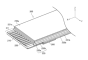
- It is a perspective view showing an example of a shield flat cable with which a connector concerning this indication is equipped. It is a figure for demonstrating the arrangement
- NEXT Near End Cross Crosstalk
- FEXT Near End Cross Crosstalk
- a shielded flat cable for high-speed signal transmission a plurality of conductors are generally arranged with ground lines on both sides of a two-core signal line.
- the ground line is dropped to the ground potential on the substrate side.
- the shield layer is set to the ground potential together with the ground line. The method of dropping can be considered. The inventor has found that the latter method of connecting the shield layer to the ground line and dropping the shield layer and the ground line to the ground potential at the same time improves the transmission characteristics more than the former method using the metal shell. .
- the present disclosure has been made on the basis of these findings, and by devising the structure of the connector without requiring processing of a shielded flat cable for high-speed signal transmission, a low-cost connector with good transmission characteristics and
- the object is to provide a substrate.
- a connector includes a signal line and a ground line arranged in parallel, an insulating layer that covers the signal line and the ground line, and a first shield layer that covers both surfaces of the insulating layer. And a second shield layer, a shield flat cable in which a terminal portion in which the signal line and the ground wire are exposed at the first shield layer side at the end in the longitudinal direction is mounted, and a housing is provided.
- the connector has a bottom portion and a top portion facing the first shield layer or the second shield layer, and a side wall portion connected to the bottom portion and the top portion, and the shield flat cable is mounted.
- the signal line contact member that contacts the signal line of the terminal part, the ground line contact member that contacts the ground line of the terminal part, and the first seal A first shield layer contact member in contact with the layer; a second shield layer contact member electrically connected to the second shield layer; the ground line contact member; and the first shield layer contact member; Are electrically connected.
- the first shield layer of the shield flat cable is electrically connected to the ground wire of the shield flat cable by the first shield layer contact member and the connector ground wire contact member.
- the magnitude and variation of crosstalk in one low frequency region are greatly improved. Furthermore, since the signal line contact member and the ground line contact member can be easily mass-produced by pressing or the like, the total cost can be reduced.
- the ground wire contact member and the first shield layer contact member may be integrally formed. With this configuration, the number of parts of the connector can be reduced.
- ground line contact member and the first shield layer contact member formed integrally be longer in the insertion direction of the shield flat cable than the signal line contact member.
- the ground wire contact member and the second shield layer contact member may be electrically connected.
- the second shield layer of the shielded flat cable is electrically connected to the ground line of the shielded flat cable in the same manner as the first shield layer, so that the size and variation of the crosstalk in the low frequency region is further improved.
- the ground line contact members may be arranged on both sides of the two adjacent signal line contact members. With this configuration, it is possible to provide a connector corresponding to a differential transmission type shielded flat cable in which ground lines are arranged on both sides of two adjacent signal lines.
- the second shield layer contact member may be integrally formed with a metal shell member covering the housing. With this configuration, the noise resistance of the connector is increased.
- the metal shell member has a connection portion connected to a wiring pad having a ground potential on a substrate on which the connector is mounted.
- the metal shell member has a connection piece connected to a solder tail of the ground wire contact member.
- the metal shell member may include a cover member that covers a solder tail of the signal line contact member and the ground line contact member. With this configuration, the noise resistance characteristics of the connector are further enhanced.
- a substrate according to an aspect of the present disclosure is a substrate on which any one of the connectors (1) to (13) is mounted. With this configuration, it is possible to obtain a substrate capable of transmitting a signal with significantly improved crosstalk, which is one of important transmission characteristics, with a shielded flat cable.
- FIG. 1 is a top view illustrating an outline when a shield flat cable is attached to the connector according to the first embodiment of the present disclosure.
- FIG. 2A is a cross-sectional view taken along line IIA-IIA in FIG. 1, and is a cross-sectional view of a ground wire contact member.
- FIG. 3 is a cross-sectional view taken along line IIB-IIB in FIG. 1, and is a cross-sectional view of the signal line contact member.
- the connector 101 is installed on a printed board (PCB: Printed Circuit Board) (not shown), and performs electrical connection between the shield flat cable 200 and the printed wiring board.
- the solder tails 132 and 142 protruding from the housing 110 of the connector 101 are connected to wirings formed on the printed circuit board.
- the connector 101 has a space in which the terminal portion of the shield flat cable 200 can be attached. When the shield flat cable 200 is attached to the connector 101, a predetermined conductor of the shield flat cable 200 is connected to a predetermined portion of the printed circuit board. It is designed to be connected to the wiring.
- FIG. 3 is a perspective view showing an example of a shielded flat cable attached to the connector according to the present disclosure
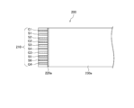
- FIG. 4 is a diagram for explaining the arrangement of conductors of the shielded flat cable shown in FIG.
- a flat cable is used in which an insulating layer 220 is formed by sandwiching both surfaces in a direction (Z direction) perpendicular to the parallel surface (XY plane) of the flat conductor 210 between the insulating layers 220a and 220b.
- one insulating layer 220a and the other insulating layer 220b are both removed to form a cable terminal portion 211 in which the flat conductor 210 is exposed.
- the cable terminal portion 211 comes into contact with a terminal (contact member) of the connector 101 when the shield flat cable 200 is attached to the connector 101.
- only one insulating layer 220a may be removed and the other insulating layer 220b may be left.
- a reinforcing plate 250 is attached to the other insulating layer 220b side of the cable terminal portion 211 to be reinforced.
- the reinforcing plate 250 is attached to the other insulating layer 220b at the location of the cable terminal portion 211.
- Dielectric layers 221a and 221b are respectively provided on the insulating layer 220 including the one insulating layer 220a and the other insulating layer 220b, and the first shield layer 230a and the second shield layer 230b are further formed thereon. It is pasted.
- the cable terminal portion 211 side of the first shield layer 230a functions as a first shield layer connecting portion that comes into contact with a first shield layer contact member described later.
- a second shield layer connection member 260 that is electrically connected to the second shield layer 230b is provided.
- the second shield layer connection member 260 is electrically connected to a second shield layer contact member of a connector described later.
- the flat conductor 210 is made of, for example, a metal such as copper foil or tin-plated annealed copper foil, has a thickness of 12 ⁇ m to 100 ⁇ m, a width of about 0.2 to 0.8 mm, and a pitch P of 0.4 to 1.5 mm. Are arranged at appropriate intervals. The arrangement of the flat conductors 210 is held between the insulating layers 220a and 220b. Although the flat conductor 210 is used for signal transmission, the predetermined flat conductor 210 is dropped to the ground potential when it is connected to the terminal of the connector on the printed circuit board side.
- FIG. 4 when the flat conductor 210 that transmits a signal is a signal line Sn (n is a positive integer) and the flat conductor 210 that is dropped to the ground potential is a ground line Gm (m is a positive integer), FIG. As shown in FIG. 4, two signal lines S and one ground line are arranged in the parallel direction (Y-axis direction) as G1-S1-S2-G2-S3-S4-G3-S5-S6-G4. G is arranged so as to be repeated.
- two adjacent signal lines S are used for differential transmission. Note that the transmission characteristics are remarkably improved by dropping the ground lines provided on both sides of the two signal lines for differential transmission to the ground potential together with the shield layer.
- two signal lines S and two lines such as G1-G2-S1-S2-G3-G4-S3-S4-G5-G6-S5-S6-G7-G8, are used. You may arrange so that the ground line G may be repeated. In this case, the arrangement of ground line contact members and signal line contact members, which will be described later, may be matched to the arrangement of ground lines G and signal lines S of the shield flat cable.
- the insulating layers 220a and 220b for example, a two-layer structure having an adhesive layer on the inner surface of the insulating film is used.
- the insulating film a general resin film having a thickness of about 9 ⁇ m to 300 ⁇ m and excellent in flexibility, for example, a polyester resin, a polyphenylene sulfide resin, a polyimide resin, or the like is used.
- the adhesive layer for example, an adhesive made of a resin material in which a flame retardant is added to a polyester resin or a polyolefin resin is used with an appropriate thickness of 10 ⁇ m to 150 ⁇ m.
- the insulating layers 220a and 220b may be formed of, for example, a polyethylene single layer resin without using an insulating film.
- the first shield layer 230a and the second shield layer 230b have an overall thickness of about 30 ⁇ m, and an aluminum foil or a copper foil provided with an adhesive layer or a resin layer is used.
- the dielectric layers 221a and 221b are provided for adjusting the characteristic impedance of the shielded flat cable 200, but are not necessarily provided.
- a protective layer may be provided on the first shield layer 230a and the second shield layer 230b. When providing a protective layer, it can provide over the perimeter of the shield flat cable 200 except the edge part side of the 1st shield layer 230a and the 2nd shield layer connection member 260. FIG.
- the connector 101 is an example of a non-zero-interpose-non (NON-ZIF) connector, and includes a housing 110 made of an electrically insulating resin.
- the housing 110 includes a bottom portion 111, a side wall portion 112, and a top portion 113, and four types of contact members are fixed inside the housing 110.
- the first of the four types of contact members is a ground wire contact member 130A that contacts the ground line G of the shield flat cable 200
- the second is a first contact that contacts the first shield layer 230a of the shield flat cable 200.
- This is a shield layer contact member 130B.
- the third is a signal line contact member 140 that contacts the signal line S
- the fourth is a second shield layer contact member 180 that contacts the second shield layer connection member 260.
- the ground wire contact member 130A and the first shield layer contact member 130B are integrally formed.
- the integrally formed ground line contact member 130A and the first shield layer contact member 130B are hereinafter referred to as an integrated ground line contact member 130.
- the integrated ground wire contact member 130 is one form for electrically connecting the ground wire contact member 130A and the first shield layer contact member 130B.
- the arrangement of the integrated ground wire contact member 130 and the signal line contact member 140 is arranged so as to correspond to the ground line G and the signal line S of the shielded flat cable 200 to be mounted.
- the flat conductor 210 of the shielded flat cable 200 is arranged so that two signal lines S and one ground line G are repeated as shown in FIG. 4, two adjacent signals
- the integrated ground wire contact members 130 are disposed on both sides of the line contact member 140, respectively.
- FIG. 2A shows a cross-sectional view in the XZ plane passing through the center of the ground line G when the shield flat cable 200 is attached to the connector 101.
- the shield flat cable 200 is a flat conductor 210 of the cable terminal 211. Are exposed to the connector 101 so that the exposed surface faces the top 113 side of the connector 101.
- the integrated ground wire contact member 130 has an arm portion 131 and a solder tail 132, and is fixed to the side wall portion 112 at a portion from the base portion of the arm portion 131 to the base portion of the solder tail 132.
- the integrated ground wire contact member 130 is made of a metal material having conductivity and good spring properties, such as brass or phosphor bronze.
- the arm portion 131 of the integrated ground wire contact member 130 has a ground wire contact portion 133 as a ground wire contact member 130A protruding toward the bottom 111 side on the base side (side wall portion 112 side), and a distal end portion.
- the first shield layer contact portion 134 as the first shield layer contact member 130B that protrudes toward the bottom 111 side is integrally provided on the side (the side opposite to the side wall portion 112 side).
- the ground wire contact portion 133 and the first shield layer contact portion 134 may each be configured as a protrusion having elasticity.
- a second shield layer contact member 180 is provided at a position facing the second shield layer connection member 260 of the shield flat cable 200.
- the second shield layer contact member 180 is provided on the bottom portion 111 of the housing 110, and the second shield layer contact portion 181 that contacts the second shield layer connection member 260 of the shield flat cable 200 and the ground potential of the substrate.
- the ground potential connection portion 182 connected to the wiring is provided.
- the ground potential connecting portion 182 may be dropped to the ground potential of the substrate through the metal shell.
- a metal material having conductivity and good spring properties such as brass and phosphor bronze, is used, like the ground wire contact member 130A.
- the ground wire contact portion 133 of the ground wire contact member 130A contacts the ground wire G of the shield flat cable 200, and the first shield layer contact portion 134 is shield flat.
- the second shield layer contact member 181 of the second shield layer contact member 180 is in contact with the second shield layer connection member 260.
- the dimensions of the shield flat cable 200 and each contact member are adjusted so as to obtain an appropriate contact pressure.
- the first shield layer contact part 134, the second shield layer contact part 181 and the ground wire contact part 133 are sequentially located from the entrance side of the shield flat cable 200 in the insertion direction.
- the solder tail 132 is connected to a pad of a wiring that is dropped to the ground potential of a printed board (not shown) using solder or the like.
- the ground line G of the shield flat cable 200 and the first shield layer 230a are dropped to the ground potential of the printed circuit board via the integrated ground line contact member 130, and the second shield of the shield flat cable 200 is provided.
- the layer 230b is also dropped to the ground potential of the printed circuit board via the second shield layer connecting member 260 and the second shield layer contact member 180.
- the signal line contact member 140 has an arm portion 141 and a solder tail 142, and is fixed to the side wall portion 112 at a portion from the base portion of the arm portion 141 to the base portion of the solder tail 142. Yes.
- a metal material having conductivity and good spring property such as brass or phosphor bronze, is used, like the ground line contact member 130A.
- the arm portion 141 of the signal line contact member 140 integrally has a signal line contact portion 143 protruding toward the bottom 111 side on the base side (side wall portion 112 side). In the present embodiment, the signal line contact member 140 is shorter than the integral ground line contact member 130 in the insertion direction of the shield flat cable.
- a second shield layer contact member 180 similar to the second shield layer contact member 180 shown in FIG. 2A may be provided at a position facing the second shield layer connection member 260 of the shield flat cable 200. Good.
- the second shield layer contact member 180 can be electrically connected to the second shield layer 230b as long as it comes into contact with the second shield layer connection member 260 of the shield flat cable 200 provided in a planar shape. It can be provided not only at the position shown in FIG. In the present embodiment, it is assumed that the second shield layer contact member 180 is in the illustrated position.
- the signal line contact portion 143 of the signal line contact member 140 is in contact with the signal line S of the shield flat cable 200, and further, the second shield layer contact member 180 The dimension of each part is adjusted so that the 2nd shield layer contact part 181 may contact the 2nd shield layer connection member 260.
- the solder tail 142 is connected to a signal wiring pad of a printed board (not shown) using solder or the like.
- the signal line S of the shield flat cable 200 is connected to the signal wiring of the printed circuit board via the signal line contact member 140, and the second shield layer 230b of the shield flat cable 200 is also connected to the second shield layer 230b.
- the potential is dropped to the ground potential of the printed circuit board.
- the connector 101 according to the present embodiment is effective even when the first shield layer 230a and the second shield layer 230b of the shield flat cable 200 are electrically connected, but on the insulating layers 220a and 220b, respectively. This is particularly effective when formed independently, that is, when the first shield layer 230a and the second shield layer 230b provided on the upper and lower surfaces are not electrically connected.
- the connector 101 has the first shield layer 230a on one side of the shielded flat cable 200 via the integrated ground wire contact member 130, and the second shield layer 230b on the other side. It becomes possible to drop to the ground potential of the substrate via the shield layer contact member 180.
- the method of attaching the shield flat cable 200 to the connector 101 is to insert the shield flat cable 200 from the opening on the opposite side of the side wall portion 112 of the housing 110, and the tip of the shield flat cable 200 is at a predetermined position, for example, the side wall portion 112. It suffices to push it down to the position where it abuts. Further, when the shield flat cable 200 is removed from the connector 101, the shield flat cable 200 may be pulled out from the connector 101.
- FIG. 5 is a cross-sectional view of the ground wire contact member when the shield flat cable is attached to the connector according to the second embodiment of the present disclosure.
- the cross-section and configuration of the signal line contact member are the same as those in the first embodiment, and thus illustration and description thereof are omitted.
- the ground line contact member 130A and the first shield layer contact member 130B are integrally formed.
- the contact member 130A and the first shield layer contact member 130B are configured separately.
- the ground wire contact member 130 ⁇ / b> A is fixed to the side wall portion 112 of the housing 110, and includes a ground wire contact portion 133 that protrudes toward the bottom portion 111, and a solder tail 132.
- the first shield layer contact member 130B is fixed to the top portion 113 of the housing 110, for example, and has a first shield layer contact portion 134 that protrudes toward the bottom 111 side.
- the ground wire contact member 130A is provided with a connection piece 135, and the first shield layer contact member 130B is provided with a connection piece 136 capable of contacting the connection piece 135.
- the ground wire contact portion 133 of the ground wire contact member 130A contacts the ground wire G of the shield flat cable 200, and the first shield layer contact member 130B.
- the first shield layer contact portion 134 contacts the first shield layer 230 a of the shield flat cable 200.
- the connection piece 135 provided on the ground line contact member 130A comes into contact with the connection piece 136 provided on the first shield layer contact member 130B.
- the first shield layer 230a of the shielded flat cable 200 is dropped to the ground potential of the printed circuit board (not shown) together with the ground line G via the first shield layer contact member 130B and the ground line contact member 130A. Since other configurations are the same as those of the connector 101 of the first embodiment, the description thereof is omitted.
- the pressing force when each contact member contacts the shield flat cable 200 is individually set. It becomes possible to adjust.
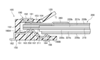
- FIG. 6A is a cross-sectional view of a ground wire contact member when a shielded flat cable is attached to a connector according to a third embodiment of the present disclosure
- FIG. 6B illustrates a third embodiment of the present disclosure. It is sectional drawing in the location of the contact member for signal wires at the time of attaching a shield flat cable to the connector concerned.
- the connector 103 is another example of a ZIF (Zero Interpose Force: no insertion force) connector, and includes a housing 150 made of an electrically insulating resin.
- the housing 150 includes a bottom portion 151, a side wall portion 152, and a top portion 153. Further, a hinge portion 154 is provided on the tip side of the top portion 153, and the flip lock member 120 is rotatably attached via the hinge portion 154.
- ZIF Zero Interpose Force: no insertion force
- the shield flat cable 200 is inserted into the connector 103 such that the exposed surface of the flat conductor 210 of the cable terminal portion 211 faces the bottom 151 side of the connector 103.
- four types of contact members are fixed inside the housing 110.
- the first of the four types of contact members is a ground wire contact member 160A that contacts the ground line G of the shield flat cable 200
- the second is a first contact that contacts the first shield layer 230a of the shield flat cable 200.
- This is a shield layer contact member 160B.
- the third is a signal line contact member 170 in contact with the signal line S
- the fourth is a second shield layer contact member 190 in contact with the second shield layer connection member 260.
- the ground wire contact member 160A and the first shield layer contact member 160B are integrally formed.
- the integrated ground wire contact member 160 is one form for electrically connecting the ground wire contact member 160A and the first shield layer contact member 160B.
- the integrally formed ground line contact member 160A and the first shield layer contact member 160B are hereinafter referred to as an integrated ground line contact member 160.
- two types of contact members that is, an integral ground wire contact member 160 and a signal line contact member 170 are provided on the bottom portion 151 and the side wall portion 152 of the housing 150.
- the top portion 153 is provided with a second shield layer contact member 190.
- the arrangement of the integrated ground line contact member 160 and the signal line contact member 170 is arranged to correspond to the ground line G and the signal line S of the shielded flat cable 200 to be mounted.
- the integrated ground wire contact member 160 includes an arm portion 161 and a solder tail 162, and the integrated ground wire contact member 160 includes the bottom portion 151 and the side wall portion 152 of the housing 150. At the same time, it is integrally manufactured by insert molding, for example.
- the integrated ground wire contact member 160 is made of a metal material having conductivity and good spring properties, such as brass or phosphor bronze.
- the arm portion 161 of the integrated ground wire contact member 160 has a ground wire contact portion 163 as an integrated ground wire contact member 160 protruding toward the top portion 153 on the base side (side wall portion 152 side);
- a first shield layer contact portion 164 as a first shield layer contact member 160B that protrudes toward the top portion 153 side is provided on the tip end side (the side opposite to the side wall portion 152 side).
- the solder tail 162 provided at the portion protruding from the side wall portion 152 is connected to a pad of a ground potential wiring of a printed board (not shown) using solder or the like.
- a second shield layer contact member 190 is provided at a position facing the second shield layer connection member 260 of the shield flat cable 200.
- the second shield layer contact member 190 is provided on the top portion 153 of the housing 150, and the second shield layer contact portion 191 that contacts the second shield layer connection member 260 of the shield flat cable 200 and the ground potential connection portion. 192.
- the ground potential connection 192 is connected to a metal shell that is dropped to the ground potential of the substrate.
- a metal material having conductivity and good spring properties for example, brass, phosphor bronze, etc., is used as in the case of the integrated ground wire contact member 160.
- the ground wire contact portion 163 of the integrated ground wire contact member 160 contacts the ground wire G of the shield flat cable 200, and the first shield layer contact portion 164.
- the solder tail 162 is connected to a signal wiring pad of a printed board (not shown) using solder or the like.
- the ground line G and the first shield layer 230a of the shield flat cable 200 are dropped to the ground potential of the printed circuit board via the integrated ground line contact member 160, and the second shield of the shield flat cable 200
- the layer 230b is also reliably dropped to the ground potential of the printed circuit board via the second shield layer connecting member 260, the second shield layer contact member 190, and the metal shell of the connector 103.
- the signal line contact member 170 has an arm portion 171 and a solder tail 172.
- the signal line contact member 170 is, for example, an insert together with the bottom portion 151 and the side wall portion 152 of the housing 150. It is produced integrally by molding.
- the signal line contact member 170 is made of a metal material having conductivity and good spring properties, for example, brass, phosphor bronze, and the like, like the integrated ground line contact member 160.
- the arm portion 171 of the signal line contact member 170 integrally has a signal line contact portion 173 projecting toward the top portion 153 side on the base side (side wall portion 152 side). In this embodiment, the signal line contact member 170 is shorter than the integrated ground line contact member 160 in the insertion direction of the shield flat cable.
- a second shield layer contact member 190 similar to the second shield layer contact member 190 shown in FIG. 6A is provided at a position facing the second shield layer connection member 260 of the shield flat cable 200.
- the second shield layer contact member 190 can be electrically connected to the second shield layer 230b as long as the second shield layer contact member 190 contacts the second shield layer connection member 260 of the shield flat cable 200 provided in a planar shape.
- the shield layer contact member is described as being at the illustrated position.
- the signal line contact portion 173 of the signal line contact member 170 is in contact with the signal line S of the shield flat cable 200, and further, the second shield layer contact member 190 is The dimension of each part is adjusted so that the 2nd shield layer contact part 191 may contact the 2nd shield layer connection member 260.
- the solder tail 172 is connected to a signal wiring pad of a printed board (not shown) using solder or the like. Then, by rotating the flip lock member 120 in the direction of the arrow, the signal line contact portion 173 reliably contacts the signal line S of the shield flat cable 200 and the shield flat cable 200 is prevented from being detached from the connector 102. Is done.
- the signal line S of the shield flat cable 200 is connected to the signal wiring of the printed circuit board via the signal line contact member 170, and the second shield layer 230b of the shield flat cable 200 is also second. It is dropped to the ground potential of the printed circuit board through the shield layer connecting member 260, the second shield layer contact member 190, and the metal shell of the connector 104.
- the connector 103 is also effective when the first shield layer 230a and the second shield layer 230b of the shield flat cable 200 are electrically connected. However, it is particularly effective when formed independently on the insulating layers 220a and 220b, that is, when the shield layers 230 provided on the upper and lower surfaces are not electrically connected. In this case, the connector 103 is connected to the first shield layer 230a on one surface of the shielded flat cable 200 via the integrated ground wire contact member 160, and the second shield layer 230b on the other surface is the second shield layer 230b. It becomes possible to drop to the ground potential of the substrate via the shield layer contact member 190.
- a method of attaching the shield flat cable 200 to the connector 103 is that the flip lock member 120 is rotated in a direction opposite to the arrow direction (counterclockwise direction), and the shield flat cable 200 is attached to the side wall portion 152 of the housing 150. Insert from the opening located opposite to. The shield flat cable 200 is inserted to a predetermined position, for example, a position where it comes into contact with the side wall 152. Then, the flip lock member 120 is rotated in the arrow direction (clockwise direction). When removing the shield flat cable 200 from the connector 102, the flip lock member 120 is rotated in the direction opposite to the arrow direction, and the shield flat cable 200 is pulled out from the connector 102.
- FIG. 7 is a cross-sectional view of the ground wire contact member when the shield flat cable is attached to the connector according to the fourth embodiment of the present disclosure.
- the cross section and the configuration of the signal line contact member are the same as those of the third embodiment shown in FIG.
- the ground line contact member 160A and the first shield layer contact member 160B are integrally formed.
- the ground line contact is formed.
- the member 160A and the first shield layer contact member 160B are configured separately.
- the ground wire contact member 160 ⁇ / b> A is fixed to the side wall portion 112 and the bottom portion 151 of the housing 110, and includes a ground wire contact portion 163 that protrudes toward the top portion 153, and a solder tail 162.
- the first shield layer contact member 160B is fixed to, for example, the bottom portion 151 of the housing 110, and has a first shield layer contact portion 164 protruding toward the top portion 153 side.
- the ground line contact member 130A is provided with a connection piece 165
- the first shield layer contact member 160B is provided with a connection piece 166 that can contact the connection piece 165.
- the ground wire contact portion 163 of the ground wire contact member 160A contacts the ground wire G of the shield flat cable 200, and the first shield layer contact member 160B.
- the first shield layer contact portion 164 contacts the first shield layer 230 a of the shield flat cable 200.
- the connection piece 165 provided on the ground line contact member 160A and the connection piece 166 provided on the first shield layer contact member 160B come into contact with each other.
- the first shield layer 230a of the shielded flat cable 200 is connected to the ground potential of the printed circuit board (not shown) together with the ground line G via the first tail shield layer contact member 160B and the solder tail 162 of the ground line contact member 160A. Is dropped. Since other configurations are the same as those of the connector 103 of the third embodiment, the description thereof is omitted.
- the pressing force when each contact member contacts the shield flat cable 200 is individually set. It becomes possible to adjust.
- FIG. 8 shows that when the connector has a metal shell, the shield layer of the shielded flat cable is dropped to the ground potential via the metal shell and the NEXT (Near End Crosstalk: near end crosstalk) according to the embodiment of the present disclosure.
- FIG. 9 is a diagram showing characteristics of the talk), and FIG. 9 shows a case where the shield layer of the shielded flat cable is dropped to the ground potential via the metal shell and a case according to the embodiment of the present disclosure when the connector has the metal shell.
- the crosstalk in the frequency band of about 4 GHz or less is significantly lower in the embodiment of the present disclosure than in the case of using the metal shell. Has also been reduced. Further, although the crosstalk in the frequency band of about 4 GHz or more is slightly larger in the embodiment of the present disclosure than in the case of using the metal shell, it is ⁇ 30 bB or less, so it is not a problem.
- the crosstalk in the frequency band of approximately 5 GHz or less is significantly lower in the embodiment of the present disclosure than in the case of using the metal shell, and varies. The reduction of is also remarkable.
- the crosstalk in the frequency band of about 5 GHz to about 12 GHz is slightly larger in the embodiment of the present disclosure than in the case of using the metal shell, the metal shell is used in the frequency band of about 12 GHz or more.
- the case of the embodiment of the present disclosure is significantly lower than that of the case of the above.
- the transmission characteristics of NEXT and FEXT are more than the case where the shield layer of the shielded flat cable is dropped to the ground potential using the metal shell of the connector as shown in characteristic 2.
- FIG. 10 is a cross-sectional view of the ground wire contact member when the shield flat cable is attached to the connector according to the fifth embodiment of the present disclosure.
- the cross section and the configuration of the signal line contact member are the same as those of the third embodiment shown in FIG.
- the ground wire contact member 160A and the first shield layer contact member 160B are configured separately.
- the ground wire contact member 160 ⁇ / b> A is fixed to the side wall portion 112 and the bottom portion 151 of the housing 110, and includes a ground wire contact portion 163 that protrudes toward the top portion 153, and a solder tail 162.
- the first shield layer contact member 160B is fixed to, for example, the bottom portion 151 of the housing 110, and the first shield layer contact portion 164 protruding toward the top portion 153 side is also directed toward the top portion 153 side. It has a ground wire contact portion 167 protruding in this manner.
- the first shield layer contact member 160B has the ground potential connection portion 168, but the ground potential connection portion 168 may not be provided.
- the ground wire contact portion 163 of the ground wire contact member 160A contacts the ground wire G of the shield flat cable 200, and the first shield layer contact member 160B.
- the first shield layer contact portion 164 contacts the first shield layer 230 a of the shield flat cable 200.
- the ground wire contact portion 167 of the first shield layer contact member 160 ⁇ / b> B contacts the ground wire G of the shield flat cable 200.
- the first shield layer 230a of the shield flat cable 200 is illustrated together with the ground line G via the first shield layer contact member 160B, the ground line G, and the solder tail 162 of the first shield layer contact member 160B. Do not drop to the ground potential of the printed circuit board.
- the ground potential connection portion 168 is provided in the first shield layer contact member 160B, the first shield layer 230a and the ground line G of the shield flat cable 200 are further passed through the ground potential connection portion 168 and a printed board (not shown). To the ground potential.
- the present embodiment is an example in which the ground line contact member 160A and the first shield layer contact member 160B are electrically connected using the ground line G of the shield flat cable 200. Since other configurations are the same as those of the connector 103 of the third embodiment, the description thereof is omitted.
- FIG. 11 is a cross-sectional view of a ground wire contact member when a shield flat cable is attached to the connector according to the sixth embodiment of the present disclosure.
- the connector 106 of the present embodiment includes a ground wire contact member 160 ⁇ / b> A that contacts the ground wire G of the shield flat cable 200, and the first shield layer of the shield flat cable 200.
- the contact member 160 for 1st shield layers which contacts 230a is integrally formed, and it has the contact member 160 for integrated ground wires formed integrally.
- the connector 106 is provided with a second shield layer contact member 190 ′ at a position facing the second shield layer connection member 260 of the shield flat cable 200.
- the second shield layer contact member 190 ′ includes a second shield layer contact portion 191 that contacts the second shield layer connection member 260 of the shield flat cable 200, and a connection piece 193 that extends to the ground wire contact member 160A. Yes.
- the ground wire contact portion 163 of the integrated ground wire contact member 160 contacts the ground wire G of the shield flat cable 200 and the first shield layer contact portion 164. Contacts the first shield layer 230a of the shielded flat cable 200. Further, the second shield layer contact portion 191 of the second shield layer contact member 190 ′ contacts the second shield layer connection member 260. As a result, the ground line G, the first shield layer 230a, and the second shield layer 230b of the shield flat cable 200 are dropped to the ground potential of a printed board (not shown) via the common solder tail 162.
- the second shield layer contact member 190 ′ is fixed to the top portion 153 of the housing 150, but the second shield layer contact member 190 ′ may be fixed to the side wall portion 152.
- the connection piece 193 is electrically connected to the ground wire contact member 160A outside the housing 150, but the connection piece 193 is connected to the ground wire contact member 160A in the space inside the housing 150. Also good. Further, the integrated ground wire contact member 160 and the second shield layer contact member 190 ′ may be integrally formed.
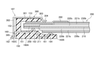
- FIG. 12A is a cross-sectional view of a ground wire contact member when a shielded flat cable is attached to a connector according to a seventh embodiment of the present disclosure
- FIG. 12B illustrates the seventh embodiment of the present disclosure. It is sectional drawing in the location of the contact member for signal wires at the time of attaching a shield flat cable to the connector concerned.
- FIG. 13 is a perspective view of a connector according to the seventh embodiment of the present disclosure.
- the connector 101 is an example of a NON-ZIF connector, and includes a casing 150 and a metal shell 300 made of electrically insulating resin.
- the housing 150 includes a bottom portion 151, a side wall portion 152, and a top portion 153, and three types of contact members are fixed inside the housing 150.
- the first of the three types of contact members is a ground wire contact member 160A that contacts the ground line G of the shield flat cable 200
- the second is a first contact that contacts the first shield layer 230a of the shield flat cable 200.
- This is a shield layer contact member 160B.
- the third is a signal line contact member 170 that contacts the signal line S.
- the connector 107 has an integrated ground wire contact member 160 in which a ground wire contact member 160A and a first shield layer contact member 160B are integrally formed. Further, the solder tail 162 'of the integrated ground wire contact member 160 is provided with a recess 162C for receiving a contact piece 305 of the metal shell 300 described later on the upper surface side.
- the signal line contact member 170 includes an arm portion 171 and a solder tail 172, and the configuration of the signal line contact member 170 is the same as that of the third embodiment.
- the metal shell 300 has an upper surface portion 301 that covers the top portion 153 of the housing 150 and a side surface portion 302 that covers the side wall portion 152 of the housing 150.
- a second shield layer contact member 303 is integrally provided on the opposite side of the side surface portion 302 at a location extending from the upper surface portion 301 and exceeding the top portion 153 of the housing 150.
- the second shield layer contact member 303 has a second shield layer contact portion 304 that is a protruding piece protruding toward the bottom 151 of the housing 150, and the second shield layer contact portion 304 is the second shield layer contact portion 304.
- the shield layer connection member 260 is contacted.
- the side surface portion 302 of the metal shell 300 extends to the solder tail 162 ′ side at a position facing the solder tail 162 ′ of the integrated ground wire contact member 160 and elastically contacts the concave portion 162C of the solder tail 162 ′.
- a contact piece 305 is provided. In the present embodiment, the contact piece 305 is configured as a protrusion having a curved tip.
- the ground wire contact portion 163 of the integrated ground wire contact member 160 comes into contact with the ground wire G of the shield flat cable 200 and is used for the first shield layer.
- the contact portion 164 contacts the first shield layer 230a of the shield flat cable 200.
- the signal line contact portion 173 of the signal line contact member 170 contacts the signal line S of the shield flat cable 200.
- the second shield layer contact portion 304 of the metal shell 300 contacts the second shield layer connection member 260 of the shield flat cable 200.
- the first shield layer 230a of the shield flat cable 200 is grounded together with the ground wire G and the ground of the printed circuit board (not shown) via the solder tail 162 'of the first shield layer contact member 160B and the ground wire contact member 160A. Dropped to potential. Further, the second shield layer 230b of the shield flat cable 200 is also dropped to the ground potential of a printed board (not shown) through the metal shell 300 and the solder tail 162 'of the ground wire contact member 160A.
- FIG. 14 is a diagram illustrating an example of a connection portion between the solder tail and the metal shell of the ground wire contact member of the connector according to the seventh embodiment of the present disclosure.
- the notch 162D is provided in the solder tail 162 ′′ of the integrated ground wire contact member 160, and the protrusion 306D provided on the side of the contact piece 306 of the metal shell 300 is fitted.
- the solder tail 162 ′′ and the metal shell 300 are electrically connected.
- the metal shell 300 is dropped to the ground potential via the solder tail 162 ′ or 162 ′′ of the ground wire contact member 160A.
- the metal shell 300 is dropped directly to the ground potential of a printed circuit board (not shown).
- side portions that cover both sides of the flat conductor 210 of the shielded flat cable 200 in the parallel direction (the Y-axis direction in FIG. 3) are integrally provided in the metal shell 300, and the side portions are directly connected to the ground potential of the printed circuit board.
- the metal shell 300 covers the housing 150, the noise resistance of the connector 107 is improved.
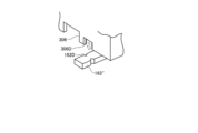
- FIG. 15 is a cross-sectional view of the ground wire contact member when a shielded flat cable is attached to the connector according to the eighth embodiment of the present disclosure
- FIG. 16 illustrates the eighth embodiment of the present disclosure. It is a figure which shows the metal shell of the connector which concerns.
- the connector 108 of the present embodiment is similar to the seventh embodiment in that it has a metal shell 300, but differs in that the metal shell 300 has a cover portion 307 that covers the solder tail 162. Further, the electrical connection between the metal shell 300 and the solder tail 162 of the ground wire contact member 160A is performed by bringing the connection piece 308 provided on the cover portion 307 into contact with the solder tail 162. As shown in FIG. 16, the connection piece 308 is formed by cutting and raising a part of the cover portion 307, but may have other configurations.
- the ground wire contact portion 163 of the integrated ground wire contact member 160 comes into contact with the ground wire G of the shield flat cable 200 and is used for the first shield layer.
- the contact portion 164 contacts the first shield layer 230a of the shield flat cable 200.
- the signal line contact portion 173 of the signal line contact member 170 (not shown) is in contact with the signal line S of the shield flat cable 200.
- the second shield layer contact portion 304 of the metal shell 300 contacts the second shield layer connection member 260 of the shield flat cable 200.
- the first shield layer 230a, the ground line G, and the second shield layer 230b of the shielded flat cable 200 are dropped to the ground potential of the printed circuit board (not shown) via the solder tail 162 of the ground line contact member 160A. It is.
- the embodiments of the present disclosure have been described.
- special processing for connecting the shield layer to the ground line for example, a comb-shaped conductor is attached or wire bonding is performed. It is not necessary to do.
- the connector can be reduced in height.
- the present invention is a connector to which a shielded flat cable having a ground wire and a shield layer is attached, and the configuration of each embodiment is as long as the contact member of the connector can contact the ground wire and the shield layer. Not limited to.
- substrate with which the connector of this invention was mounted will not ask
- this invention includes what combined arbitrary embodiment.
- contact portion for the second shield layer 182: Ground potential connection, 190 ... Contact member for second shield layer, 190 '... contact member for second shield layer, 191 ... the contact portion for the second shield layer, 192: Ground potential connection, 193 ... connection piece, 200 ... shield flat cable, 210: flat conductor, 211 ... cable terminal part, 220 ... insulating layer, 220a ... insulating layer, 220b ... insulating layer, 221a: dielectric layer, 221b ... dielectric layer, 230 ... shield layer, 230a ... 1st shield layer, 230b ... the second shield layer, 250 ... a reinforcing plate, 260 ... second shield layer connecting member, 300 ... metal shell, 301 ...
Landscapes
- Insulated Conductors (AREA)
- Coupling Device And Connection With Printed Circuit (AREA)
- Details Of Connecting Devices For Male And Female Coupling (AREA)
- Liquid Crystal Substances (AREA)
- Control Of Motors That Do Not Use Commutators (AREA)
Priority Applications (3)
| Application Number | Priority Date | Filing Date | Title |
|---|---|---|---|
| CN201980028323.2A CN112042062B (zh) | 2018-04-27 | 2019-03-28 | 连接器和基板 |
| JP2020516138A JP7294329B2 (ja) | 2018-04-27 | 2019-03-28 | コネクタおよび基板 |
| US17/049,688 US11410790B2 (en) | 2018-04-27 | 2019-03-28 | Substrate-mounted electrical connector for connecting to a shielded flat cable |
Applications Claiming Priority (2)
| Application Number | Priority Date | Filing Date | Title |
|---|---|---|---|
| JP2018017258 | 2018-04-27 | ||
| JPPCT/JP2018/017258 | 2018-04-27 |
Publications (1)
| Publication Number | Publication Date |
|---|---|
| WO2019208091A1 true WO2019208091A1 (ja) | 2019-10-31 |
Family
ID=68295158
Family Applications (2)
| Application Number | Title | Priority Date | Filing Date |
|---|---|---|---|
| PCT/JP2019/013705 Ceased WO2019208091A1 (ja) | 2018-04-27 | 2019-03-28 | コネクタおよび基板 |
| PCT/JP2019/017803 Ceased WO2019208737A1 (ja) | 2018-04-27 | 2019-04-25 | シールドフラットケーブル |
Family Applications After (1)
| Application Number | Title | Priority Date | Filing Date |
|---|---|---|---|
| PCT/JP2019/017803 Ceased WO2019208737A1 (ja) | 2018-04-27 | 2019-04-25 | シールドフラットケーブル |
Country Status (5)
| Country | Link |
|---|---|
| US (3) | US11410790B2 (https=) |
| JP (3) | JP7294329B2 (https=) |
| CN (2) | CN112042062B (https=) |
| TW (1) | TWI802683B (https=) |
| WO (2) | WO2019208091A1 (https=) |
Cited By (3)
| Publication number | Priority date | Publication date | Assignee | Title |
|---|---|---|---|---|
| WO2022172967A1 (ja) * | 2021-02-12 | 2022-08-18 | I-Pex株式会社 | コネクタ及びコネクタ装置 |
| WO2024057447A1 (ja) * | 2022-09-14 | 2024-03-21 | エレファンテック株式会社 | コネクタ接続構造及びその製造方法 |
| US12183093B2 (en) | 2020-10-08 | 2024-12-31 | Magna Electronics Sweden Ab | Driver monitoring system based on vision camera |
Families Citing this family (18)
| Publication number | Priority date | Publication date | Assignee | Title |
|---|---|---|---|---|
| WO2019208091A1 (ja) * | 2018-04-27 | 2019-10-31 | 住友電気工業株式会社 | コネクタおよび基板 |
| JP6715411B2 (ja) * | 2018-07-27 | 2020-07-01 | 株式会社テクノ・コア | 信号伝送用フラットケーブル及びその製造方法 |
| JP7134934B2 (ja) * | 2019-10-08 | 2022-09-12 | ヒロセ電機株式会社 | 導電部材を保持する保持部材を有するコネクタ |
| JP7412129B2 (ja) * | 2019-10-24 | 2024-01-12 | 株式会社Totoku | フラットケーブル |
| TWM595899U (zh) * | 2019-12-06 | 2020-05-21 | 貿聯國際股份有限公司 | 電路板結構及具有該電路板結構的連接器 |
| WO2022004074A1 (ja) * | 2020-07-02 | 2022-01-06 | 住友電気工業株式会社 | シールドフラットケーブル |
| US11875912B2 (en) | 2020-07-02 | 2024-01-16 | Sumitomo Electric Industries, Ltd. | Shielded flat cable |
| JP7634555B2 (ja) * | 2020-11-16 | 2025-02-21 | 株式会社フジクラ | 配線板及び配線板の製造方法 |
| WO2022209843A1 (ja) * | 2021-03-30 | 2022-10-06 | 株式会社オートネットワーク技術研究所 | 通信器及び通信装置 |
| JP7608265B2 (ja) * | 2021-05-13 | 2025-01-06 | 日本航空電子工業株式会社 | コネクタ・ケーブル |
| CN115832789A (zh) * | 2021-09-17 | 2023-03-21 | 叶时堃 | 讯号传输装置 |
| CN113936846A (zh) * | 2021-09-30 | 2022-01-14 | 荣成歌尔科技有限公司 | 双面导体ffc线缆及其连接器 |
| TWM627234U (zh) * | 2021-11-19 | 2022-05-21 | 英豪科技股份有限公司 | 嵌入成型連接器 |
| EP4191805B1 (en) * | 2021-12-02 | 2025-10-01 | Nexans | High voltage power distributor |
| JP7633533B2 (ja) | 2022-06-14 | 2025-02-20 | 山一電機株式会社 | 高周波信号伝送装置、及び配線基板とコネクタの電気的接続方法 |
| TWI841302B (zh) * | 2023-03-17 | 2024-05-01 | 英業達股份有限公司 | 伺服器 |
| WO2024228285A1 (ja) * | 2023-05-02 | 2024-11-07 | 住友電気工業株式会社 | ワイヤハーネス、検知システム、および、検知方法 |
| WO2025219806A1 (en) * | 2024-04-15 | 2025-10-23 | Molex, Llc | Conductive inlay grounding and shielding |
Citations (3)
| Publication number | Priority date | Publication date | Assignee | Title |
|---|---|---|---|---|
| US5254010A (en) * | 1992-09-16 | 1993-10-19 | Amp Incorporated | Securing a surface mount electrical connector in a metal shielding shell |
| JP2008027707A (ja) * | 2006-07-20 | 2008-02-07 | Taiko Denki Co Ltd | フレキシブル基板用のコネクタ |
| US20150364846A1 (en) * | 2014-06-12 | 2015-12-17 | Chung-Hao J. Chen | Flat flexible cable connector with grounding |
Family Cites Families (30)
| Publication number | Priority date | Publication date | Assignee | Title |
|---|---|---|---|---|
| JPS6123128U (ja) * | 1984-07-12 | 1986-02-10 | 日立電線加工株式会社 | 耐腐蝕性補強板付きテ−プ電線 |
| AU573099B2 (en) * | 1985-08-19 | 1988-05-26 | Thomas & Betts Corporation | Flat multiconductor cable for undercarpet wiring |
| US5658164A (en) * | 1995-03-24 | 1997-08-19 | The Whitaker Corporation | Flexible flat electrical cable connector with a conductive shield |
| JPH08287733A (ja) * | 1995-04-18 | 1996-11-01 | Fujikura Ltd | シールド付フラットケーブル |
| JP2000149668A (ja) * | 1998-11-13 | 2000-05-30 | Totoku Electric Co Ltd | 端末保護フィルム貼付フラットケーブル |
| JP2002150848A (ja) * | 2000-11-10 | 2002-05-24 | Fujikura Ltd | シールドフラットケーブル及びその接続方法 |
| JP2002231063A (ja) * | 2001-01-31 | 2002-08-16 | Fujikura Ltd | シールドフラットケーブル及びその製造方法 |
| EP1727161A1 (en) * | 2005-05-23 | 2006-11-29 | 3M Innovative Properties Company | Flat cable shield ground connection |
| JP5119898B2 (ja) | 2007-12-13 | 2013-01-16 | 住友電気工業株式会社 | シールドフラットケーブル |
| JP4570107B2 (ja) | 2008-04-23 | 2010-10-27 | 日本航空電子工業株式会社 | コネクタ |
| JP4363664B1 (ja) * | 2009-01-26 | 2009-11-11 | 坂東電線株式会社 | フレキシブルフラットケーブル |
| JP2010192287A (ja) * | 2009-02-19 | 2010-09-02 | Sumitomo Electric Ind Ltd | 高速伝送用フレキシブルフラット高周波ケーブル端末接続構造及びその製造方法 |
| KR101056324B1 (ko) * | 2009-03-09 | 2011-08-11 | 스미토모 덴키 고교 가부시키가이샤 | 시일드 플랫 케이블 |
| CN101840749B (zh) | 2009-03-20 | 2012-05-23 | 住友电气工业株式会社 | 屏蔽扁平电缆 |
| JP2011008978A (ja) | 2009-06-24 | 2011-01-13 | Kyocera Elco Corp | 中継コネクタ |
| JP5499722B2 (ja) * | 2010-01-12 | 2014-05-21 | 住友電気工業株式会社 | シールドフラットケーブル |
| JP5293661B2 (ja) * | 2010-03-23 | 2013-09-18 | 住友電気工業株式会社 | フラットケーブル |
| KR101057088B1 (ko) * | 2011-02-16 | 2011-08-16 | (주) 우주케이에프씨 | 환형도체를 사용한 플렉시블 플랫 케이블 |
| CN202076032U (zh) * | 2011-04-02 | 2011-12-14 | 住友电气工业株式会社 | 屏蔽扁平电缆 |
| JP5866818B2 (ja) * | 2011-06-27 | 2016-02-24 | 山一電機株式会社 | 補強板付きケーブルおよび補強板 |
| JP5796256B2 (ja) * | 2011-12-15 | 2015-10-21 | ホシデン株式会社 | フレキシブルフラットケーブル |
| US20130337676A1 (en) * | 2012-06-07 | 2013-12-19 | Ant Precision Industry Co., Ltd. | Cable Connector |
| TWI614944B (zh) * | 2013-01-17 | 2018-02-11 | 星電股份有限公司 | 基板邊緣連接器 |
| JP6002620B2 (ja) | 2013-04-15 | 2016-10-05 | 矢崎総業株式会社 | シールドコネクタ |
| JP5854008B2 (ja) * | 2013-08-09 | 2016-02-09 | 住友電気工業株式会社 | フラットケーブル |
| JP6354511B2 (ja) * | 2014-10-07 | 2018-07-11 | 住友電気工業株式会社 | フラットケーブルおよびフラットケーブルの製造方法。 |
| JP2017139180A (ja) * | 2016-02-05 | 2017-08-10 | 坂東電線株式会社 | フレキシブルフラットケーブルおよびその製造方法 |
| JP6721104B2 (ja) | 2017-02-28 | 2020-07-08 | 住友電気工業株式会社 | シールドフラットケーブル |
| JP6856436B2 (ja) | 2017-04-20 | 2021-04-07 | 東京特殊電線株式会社 | フラットケーブル |
| WO2019208091A1 (ja) * | 2018-04-27 | 2019-10-31 | 住友電気工業株式会社 | コネクタおよび基板 |
-
2019
- 2019-03-28 WO PCT/JP2019/013705 patent/WO2019208091A1/ja not_active Ceased
- 2019-03-28 JP JP2020516138A patent/JP7294329B2/ja active Active
- 2019-03-28 US US17/049,688 patent/US11410790B2/en active Active
- 2019-03-28 CN CN201980028323.2A patent/CN112042062B/zh active Active
- 2019-04-19 TW TW108113896A patent/TWI802683B/zh active
- 2019-04-25 JP JP2020515586A patent/JP6923077B2/ja active Active
- 2019-04-25 CN CN201980028299.2A patent/CN112106151B/zh active Active
- 2019-04-25 US US17/049,694 patent/US11289241B2/en active Active
- 2019-04-25 WO PCT/JP2019/017803 patent/WO2019208737A1/ja not_active Ceased
-
2021
- 2021-07-28 JP JP2021122984A patent/JP7136288B2/ja active Active
-
2022
- 2022-02-15 US US17/651,121 patent/US11715582B2/en active Active
Patent Citations (3)
| Publication number | Priority date | Publication date | Assignee | Title |
|---|---|---|---|---|
| US5254010A (en) * | 1992-09-16 | 1993-10-19 | Amp Incorporated | Securing a surface mount electrical connector in a metal shielding shell |
| JP2008027707A (ja) * | 2006-07-20 | 2008-02-07 | Taiko Denki Co Ltd | フレキシブル基板用のコネクタ |
| US20150364846A1 (en) * | 2014-06-12 | 2015-12-17 | Chung-Hao J. Chen | Flat flexible cable connector with grounding |
Cited By (5)
| Publication number | Priority date | Publication date | Assignee | Title |
|---|---|---|---|---|
| US12183093B2 (en) | 2020-10-08 | 2024-12-31 | Magna Electronics Sweden Ab | Driver monitoring system based on vision camera |
| WO2022172967A1 (ja) * | 2021-02-12 | 2022-08-18 | I-Pex株式会社 | コネクタ及びコネクタ装置 |
| JP2022123660A (ja) * | 2021-02-12 | 2022-08-24 | I-Pex株式会社 | コネクタ及びコネクタ装置 |
| JP7608855B2 (ja) | 2021-02-12 | 2025-01-07 | I-Pex株式会社 | コネクタ及びコネクタ装置 |
| WO2024057447A1 (ja) * | 2022-09-14 | 2024-03-21 | エレファンテック株式会社 | コネクタ接続構造及びその製造方法 |
Also Published As
| Publication number | Publication date |
|---|---|
| WO2019208737A1 (ja) | 2019-10-31 |
| CN112042062A (zh) | 2020-12-04 |
| US11410790B2 (en) | 2022-08-09 |
| TW201946342A (zh) | 2019-12-01 |
| US20210249153A1 (en) | 2021-08-12 |
| CN112106151A (zh) | 2020-12-18 |
| CN112106151B (zh) | 2022-07-08 |
| JP7136288B2 (ja) | 2022-09-13 |
| US20220172861A1 (en) | 2022-06-02 |
| US20210249803A1 (en) | 2021-08-12 |
| TWI802683B (zh) | 2023-05-21 |
| JP7294329B2 (ja) | 2023-06-20 |
| JP6923077B2 (ja) | 2021-08-18 |
| US11289241B2 (en) | 2022-03-29 |
| US11715582B2 (en) | 2023-08-01 |
| JPWO2019208737A1 (ja) | 2021-05-13 |
| JP2021170553A (ja) | 2021-10-28 |
| CN112042062B (zh) | 2022-03-18 |
| JPWO2019208091A1 (ja) | 2021-05-27 |
Similar Documents
| Publication | Publication Date | Title |
|---|---|---|
| JP7294329B2 (ja) | コネクタおよび基板 | |
| US8840432B2 (en) | Circuit board and wire assembly | |
| TWI769682B (zh) | 具有電磁屏蔽功能的電連接器 | |
| US9124037B2 (en) | High speed input/output connection interface element, cable assembly and interconnection system with reduced cross-talk | |
| US7131862B2 (en) | Electrical connector with horizontal ground plane | |
| US20020157865A1 (en) | Flexible flat circuitry with improved shielding | |
| JP7446094B2 (ja) | 接続対象物、コネクタ、及びハーネス | |
| US20130264107A1 (en) | Circuit board and wire assembly | |
| JP5527840B2 (ja) | 挿入位置決め構造を有する回路配線 | |
| JPH04217101A (ja) | 同軸伝送線ーストリップ線結合カプラ | |
| US9040835B2 (en) | Attenuation reduction grounding structure for differential-mode signal transmission lines of flexible circuit board | |
| CN113725664B (zh) | 可滑动地插入插座连接器的插头连接器 | |
| CN113013680B (zh) | 连接器组件 | |
| KR20200014231A (ko) | 회로 기판 및 이를 포함하는 전자 기기 | |
| JP2017027721A (ja) | コネクタ付きケーブル | |
| US12597740B2 (en) | Connector assembly including receptacle connector and plug connector, and plug connector | |
| US6824401B2 (en) | Cable end connector assembly and method of assembling the assembly | |
| CN111727666A (zh) | 中继基板、带中继基板的差分传送用电线及带连接器的线缆 | |
| CN223246020U (zh) | 电连接器线缆总成 |
Legal Events
| Date | Code | Title | Description |
|---|---|---|---|
| 121 | Ep: the epo has been informed by wipo that ep was designated in this application |
Ref document number: 19792851 Country of ref document: EP Kind code of ref document: A1 |
|
| ENP | Entry into the national phase |
Ref document number: 2020516138 Country of ref document: JP Kind code of ref document: A |
|
| NENP | Non-entry into the national phase |
Ref country code: DE |
|
| 122 | Ep: pct application non-entry in european phase |
Ref document number: 19792851 Country of ref document: EP Kind code of ref document: A1 |