WO2019181547A1 - リレー駆動回路 - Google Patents
リレー駆動回路 Download PDFInfo
- Publication number
- WO2019181547A1 WO2019181547A1 PCT/JP2019/009236 JP2019009236W WO2019181547A1 WO 2019181547 A1 WO2019181547 A1 WO 2019181547A1 JP 2019009236 W JP2019009236 W JP 2019009236W WO 2019181547 A1 WO2019181547 A1 WO 2019181547A1
- Authority
- WO
- WIPO (PCT)
- Prior art keywords
- relay
- semiconductor element
- bipolar transistor
- electrically connected
- control input
- Prior art date
- Legal status (The legal status is an assumption and is not a legal conclusion. Google has not performed a legal analysis and makes no representation as to the accuracy of the status listed.)
- Ceased
Links
Images


Classifications
-
- H—ELECTRICITY
- H01—ELECTRIC ELEMENTS
- H01H—ELECTRIC SWITCHES; RELAYS; SELECTORS; EMERGENCY PROTECTIVE DEVICES
- H01H47/00—Circuit arrangements not adapted to a particular application of the relay and designed to obtain desired operating characteristics or to provide energising current
- H01H47/22—Circuit arrangements not adapted to a particular application of the relay and designed to obtain desired operating characteristics or to provide energising current for supplying energising current for relay coil
- H01H47/32—Energising current supplied by semiconductor device
-
- H—ELECTRICITY
- H01—ELECTRIC ELEMENTS
- H01H—ELECTRIC SWITCHES; RELAYS; SELECTORS; EMERGENCY PROTECTIVE DEVICES
- H01H47/00—Circuit arrangements not adapted to a particular application of the relay and designed to obtain desired operating characteristics or to provide energising current
- H01H47/002—Monitoring or fail-safe circuits
-
- H—ELECTRICITY
- H02—GENERATION; CONVERSION OR DISTRIBUTION OF ELECTRIC POWER
- H02H—EMERGENCY PROTECTIVE CIRCUIT ARRANGEMENTS
- H02H9/00—Emergency protective circuit arrangements for limiting excess current or voltage without disconnection
Definitions
- the technique disclosed in this specification relates to a relay drive circuit, and more particularly, to a technique that can maintain the operation state of the relay even when the power supply voltage is lowered.
- Patent Document 1 a technique described in Patent Document 1 is known as a technique that can maintain the operation state of a relay even when the power supply voltage is lowered.
- two series of first and second switches for driving a relay are provided, and a resistor is provided between the second switch and a coil of the relay.
- the relay is driven by a second switch provided with a resistor, and when the power supply voltage is lowered, the first switch is driven to save power, while the power supply voltage is lowered.
- a technique that can maintain the operating state of the relay is also disclosed.
- Patent Document 1 a semiconductor element is used for driving the relay, and a decrease in the power supply voltage decreases the control input voltage of the semiconductor element, which may adversely affect the control of the relay drive. There is sex.
- two relays (RL1, RL2) are connected in two stages, and the second stage relay (downstream relay) RL2 is the first stage relay (upstream relay).
- a diode D1 for protecting the semiconductor element Q1 may be inserted into the control input path LCN of the semiconductor element Q1 that drives the downstream relay RL2.
- the diode D1 is inserted into the control input path LCN to protect the semiconductor element Q1 from a surge from the inductive load when the load RD1 connected in parallel with the downstream relay RL2 is an inductive load such as a motor. .
- the control input voltage of the semiconductor element Q1 decreases due to the voltage drop (forward voltage) Vf of the diode D1, and depending on the degree of decrease of the battery voltage (power supply voltage) Vb, the semiconductor element Q1 is turned on, that is, downstream. There was a concern that the operating state of the relay RL2 could not be maintained.
- the power supply voltage is Provided is a relay drive circuit capable of maintaining the operating state of a downstream relay when the voltage is lower.
- the relay drive circuit disclosed in the present specification is a relay drive circuit that is provided between an upstream relay and a downstream relay that is driven according to the drive of the upstream relay, and that drives the downstream relay, A semiconductor element that switches on / off of the downstream relay, a control input path that is electrically connected to the control terminal of the semiconductor element and that is supplied with a power supply voltage via the upstream relay, and is inserted and connected to the control input path A protection element that protects the semiconductor element, and a buffer circuit that is provided between the protection element in the control input path and the control terminal of the semiconductor element and compensates for a voltage drop due to insertion of the protection element; Is provided.
- the buffer circuit compensates for the voltage drop due to the insertion of the protection element, thereby reducing the amount of decrease in the power supply voltage due to the protection element. Therefore, when driving a downstream relay serving as a load of the upstream relay, even when a protective element is inserted in the control input path of the semiconductor element, the operating state of the downstream relay is changed when the power supply voltage is lower. Can hold.
- the buffer circuit includes a PNP bipolar transistor and an NPN bipolar transistor, the emitter of the PNP bipolar transistor is connected to a power supply line, and the collector is electrically connected to the control terminal of the semiconductor element.
- the collector of the NPN bipolar transistor is electrically connected to the base of the PNP bipolar transistor, the base is electrically connected to the output side of the protection element, and the emitter is grounded.
- the protective element may be constituted by a protective diode having an anode connected to a relay contact of the upstream relay and a cathode connected to a base of the NPN bipolar transistor.
- a voltage drop (forward voltage) due to insertion of a diode can be appropriately compensated by a buffer circuit constituted by two bipolar transistors. That is, the forward voltage of the diode is approximately 0.7V, and the collector-emitter voltage of the PNP bipolar transistor is usually less than 0.7V. Therefore, when the power supply voltage is passed through the PNP-type bipolar transistor, the power supply voltage with less voltage drop can be applied to the control terminal of the semiconductor element as compared with the case where the power supply voltage is passed through the diode. That is, the voltage drop due to the insertion of the diode is appropriately compensated.
- the buffer circuit further includes a rectifier diode having an anode electrically connected to a base of the PNP bipolar transistor and a cathode electrically connected to a collector of the NPN bipolar transistor. It may be included. According to this configuration, when the power source is a battery, protection when the battery is reversely connected can be achieved.
- the relay drive circuit disclosed in this specification when driving a downstream relay serving as a load of an upstream relay, even if a protective element is inserted into the control input path of the drive semiconductor element, The operating state of the downstream relay can be maintained when the voltage is lower.
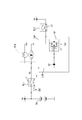
- FIG. 1 is a schematic block diagram of a relay system including a relay drive circuit according to an embodiment of the present invention.
- Schematic block diagram of a relay system including a conventional relay drive circuit Schematic block diagram of a relay system including another example relay drive circuit
- the relay drive circuit 10 is mounted on a vehicle, and the power source is a battery Ba mounted on the vehicle. Note that the relay drive circuit 10 and the power source are not limited to being mounted on a vehicle.
- the relay drive circuit 10 is provided between the upstream relay RL1 and the downstream relay RL2 driven in accordance with the drive of the upstream relay RL1, and drives the downstream relay RL2. That is, the downstream relay RL2 is in parallel with the inductive load RD1 such as the motor M with respect to the upstream relay RL1, and is turned on when the upstream relay RL1 is turned on, like the inductive load RD1.
- the relay drive circuit 10 includes a semiconductor element Q1, a control input path LCN, a protection diode D1, and a buffer circuit 20.
- the semiconductor element Q1 is configured by, for example, an N-channel MOSFET as shown in FIG. 1, and switches on / off of the downstream relay RL2 according to on / off of the upstream relay RL1. Specifically, the semiconductor element Q1 turns on / off the exciting current flowing in the exciting coil L2 of the downstream relay RL2. Bias resistors (R1, R2) are connected to the gate G of the semiconductor element Q1.
- the control input path LCN is electrically connected to the gate G which is the control terminal of the semiconductor element Q1.
- the battery voltage (power supply voltage) Vb is applied to the control input path LCN via the relay contact 1 of the upstream relay RL1.
- the protective diode D1 (an example of “protective element”) is provided by being inserted into the control input path LCN.
- the protection diode D1 protects the semiconductor element Q1 against a surge that propagates from the inductive load RD1 such as the motor M connected to the upstream relay RL1 via the control input path LCN.
- the anode A of the protection diode D1 is connected to the relay contact 1 of the upstream relay RL1 via the control input path LCN, and the cathode K is connected to the base B of an NPN bipolar transistor TR1 described later via the bias resistor R3. ing.
- the buffer circuit 20 is provided between the protection diode D1 and the gate G of the semiconductor element Q1 in the control input path LCN, and compensates for a voltage drop (forward voltage) Vf caused by the protection diode D1.
- the buffer circuit 20 includes an NPN bipolar transistor (hereinafter referred to as “NPN transistor”) TR1, a PNP bipolar transistor (hereinafter referred to as “PNP transistor”) TR2, A rectifier diode D2 and bias resistors (R3, R4, R5, R6) are included.
- NPN transistor NPN bipolar transistor
- PNP transistor PNP bipolar transistor
- a rectifier diode D2 and bias resistors (R3, R4, R5, R6) are included.
- the emitter E of the NPN transistor TR1 is connected to the ground and grounded, the collector C is connected to the cathode K of the rectifier diode D2, and is electrically connected to the base B of the PNP transistor TR2 via the rectifier diode D2 and the bias resistor R5. It is connected.
- the base B of the NPN transistor TR1 is electrically connected to the cathode K of the protection diode D1 (the output side of the protection element) via the bias resistor R3.
- the emitter E of the PNP transistor TR2 is connected to the power supply line LV, the collector C is electrically connected to the gate G of the semiconductor element Q1 via the bias resistor R1, and the base B is the anode of the rectifier diode D2 via the bias resistor R5. Connected to A.
- the anode A of the rectifier diode D2 is electrically connected to the base B of the PNP transistor TR2 via the bias resistor R5, and the cathode K is connected to the collector C of the NPN transistor.
- the rectifier diode D2 protects when the battery Ba is reversely connected. That is, when the battery Ba is connected in reverse, if the rectifier diode D2 is not provided, the current is grounded ⁇ resistor R4 ⁇ between the base B and the collector C of the NPN transistor TR1 ⁇ resistor R5 ⁇ resistor R6 ⁇ power source It will flow along the line LV. In this case, a reverse voltage is applied between the base B and the emitter E of the NPN transistor TR1 and the PNP transistor TR2, which may damage the transistor element.
- the battery voltage Vb can be applied to the gate G of the semiconductor element Q1 via the PNP transistor TR2, thereby turning on the semiconductor element Q1 and turning on the downstream relay RL2.
- the voltage drop between the collector and the emitter of the PNP transistor TR2 is usually 0.1 V or less, which is sufficiently smaller than the voltage drop Vf (usually 0.7 V) due to the protective diode D1. Therefore, compared to the conventional example shown in FIG. 2, a voltage closer to the battery voltage Vb can be applied to the gate G (specifically, bias resistors R1 and R2) of the semiconductor element Q1. Thereby, in the configuration in which the protective diode D1 is provided in the control input path LCN, the semiconductor element Q1 can be kept on even when the battery voltage Vb is lowered to a lower voltage compared to the conventional example, and the downstream relay RL2 can be turned on. Can be kept on.
- the buffer circuit 20 compensates for the voltage drop Vf due to the insertion of the protection diode D1. That is, the buffer circuit 20 reduces the amount of decrease in the battery voltage Vb due to the protection diode D1. Therefore, when the downstream relay RL2 serving as the load of the upstream relay RL1 is driven, even when the protection diode D1 is inserted into the control input path LCN of the semiconductor element (driving semiconductor element) Q1, the buffer circuit 20 The operation state of the downstream relay RL2 can be maintained when the battery voltage Vb is lower than the case where it is not provided. It leads to improved functionality and safety of the vehicle system.
- the buffer circuit 20 can appropriately compensate for the voltage drop (forward voltage) Vf due to the insertion of the protective diode D1 by a simple configuration mainly using two bipolar transistors (TR1, TR2). That is, the forward voltage of the diode is usually about 0.7V, and the voltage drop due to the on-resistance of the PNP bipolar transistor TR2 is usually 0.1V or less. Therefore, when the battery voltage Vb is applied to the gate terminal (control terminal) G of the semiconductor element Q1 through the PNP-type bipolar transistor TR2, the battery voltage Vb with a lower voltage drop is gated than in the case through the protection diode D1. It can be applied to the terminal G. That is, the voltage drop Vf due to the insertion of the protection diode D1 is reliably compensated and reduced.
- the buffer circuit 20 is configured by two bipolar transistors (TR1, TR2), but the configuration of the buffer circuit 20 is not limited to this.
- the buffer circuit 20 may be constituted by an N-channel MOSFET 1 instead of the NPN transistor TR1 and a P-channel MOSFET 2 instead of the PNP transistor TR2.
- the protection element is the protection diode D1, but the protection element is not necessarily limited to the protection diode D1.
- the protective element may be configured by a resistor having a small resistance value.
- DESCRIPTION OF SYMBOLS 10 ... Relay drive circuit 20 ... Buffer circuit Ba ... Battery (power supply) D1 ... Protective diode (protective element) D2 ... Rectifier diode G ... Gate (control terminal of semiconductor element) LCN ... control input path Q1 ... semiconductor element RL1 ... upstream relay RL2 ... downstream relay TR1 ... NPN bipolar transistor TR2 ... PNP bipolar transistor Vb ... battery voltage (power supply voltage)
Landscapes
- Relay Circuits (AREA)
- Electronic Switches (AREA)
- Keying Circuit Devices (AREA)
Abstract
リレー駆動回路10は、上流リレーRL1と、上流リレーRL1の駆動に応じて駆動される下流リレーRL2との間に設けられ、下流リレーRL2を駆動する。リレー駆動回路10は、下流リレーRL2のオン・オフをスイッチする半導体素子Q1と、半導体素子Q1の制御端子Gに電気的に接続され、上流リレーRL1を介して電源電圧Vbが印加される制御入力経路LCNと、制御入力経路LCNに挿入接続され、半導体素子Q1を保護する保護素子D1と、制御入力経路LCNにおける保護素子D1と半導体素子の制御端子Gとの間に設けられ、保護素子D1の挿入による電圧降下Vfを補償するバッファ回路20と、を備える。
Description
本明細書に開示される技術は、リレー駆動回路に関し、詳しくは、電源電圧が低下した場合であっても、リレーの動作状態を保持できる技術に関する。
従来、電源電圧が低下した場合であっても、リレーの動作状態を保持できる技術として、例えば、特許文献1に記載された技術が知られている。特許文献1では、リレーを駆動する2系列の第1、第2スイッチを設け、そのうち第2スイッチには、リレーのコイルとの間に抵抗が設けられている。そしてリレーの接点を作動させた後には、抵抗が設けられた第2スイッチによってリレーを駆動し、電源電圧が低下した場合に第1スイッチを駆動することによって省電力化しつつ、電源電圧の低下時にもリレーの動作状態を保持できる技術が開示されている。
しかしながら、近年、特許文献1にも示されるように、リレーの駆動には半導体素子が用いられおり、電源電圧の低下は半導体素子の制御入力電圧が低下し、リレー駆動の制御に悪影響を及ぼす可能性がある。
また、図2に示されるリレー駆動回路10Pのように、2個のリレー(RL1、RL2)が2段に接続され、2段目のリレー(下流リレー)RL2が1段目のリレー(上流リレー)RL1の負荷となる場合においては、下流リレーRL2を駆動する半導体素子Q1の制御入力経路LCNに、半導体素子Q1を保護するためのダイオードD1が挿入されることがある。このダイオードD1は、下流リレーRL2と並列接続される負荷RD1がモータ等の誘導性負荷である場合に、誘導性負荷からのサージから半導体素子Q1を保護するために制御入力経路LCNに挿入される。この場合、ダイオードD1の電圧降下(順方向電圧)Vfによって、半導体素子Q1の制御入力電圧が低下し、バッテリ電圧(電源電圧)Vbの低下度合いによっては、半導体素子Q1のオン状態、すなわち、下流リレーRL2の動作状態を保持できなくなる懸念があった。
そこで、本明細書に開示される技術は、上流リレーの負荷となる下流リレーを駆動する場合において、駆動用半導体素子の制御入力経路に保護素子が挿入される場合であっても、電源電圧がより低電圧である時に下流リレーの動作状態を保持できるリレー駆動回路を提供する。
本明細書に開示されるリレー駆動回路は、上流リレーと、前記上流リレーの駆動に応じて駆動される下流リレーとの間に設けられ、前記下流リレーを駆動するリレー駆動回路であって、前記下流リレーのオン・オフをスイッチする半導体素子と、前記半導体素子の制御端子に電気的に接続され、前記上流リレーを介して電源電圧が印加される制御入力経路と、前記制御入力経路に挿入接続され、前記半導体素子を保護する保護素子と、前記制御入力経路における前記保護素子と前記半導体素子の前記制御端子との間に設けられ、前記保護素子の挿入による電圧降下を補償するバッファ回路と、を備える。
本構成によれば、バッファ回路によって保護素子の挿入による電圧降下が補償され、それによって保護素子による電源電圧の低下量が低減される。そのため、上流リレーの負荷となる下流リレーを駆動する場合において、半導体素子の制御入力経路に保護素子が挿入される場合であっても、電源電圧がより低電圧である時に下流リレーの動作状態を保持できる。
本構成によれば、バッファ回路によって保護素子の挿入による電圧降下が補償され、それによって保護素子による電源電圧の低下量が低減される。そのため、上流リレーの負荷となる下流リレーを駆動する場合において、半導体素子の制御入力経路に保護素子が挿入される場合であっても、電源電圧がより低電圧である時に下流リレーの動作状態を保持できる。
上記リレー駆動回路において、前記バッファ回路は、PNP型バイポーラトランジスタと、NPN型バイポーラトランジスタと、を含み、前記PNP型バイポーラトランジスタのエミッタが電源ラインに接続され、コレクタが前記半導体素子の制御端子に電気的に接続されており、前記NPN型バイポーラトランジスタのコレクタが前記PNP型バイポーラトランジスタのベースに電気的に接続され、ベースが前記保護素子の出力側に電気的に接続され、エミッタが接地されており、前記保護素子は、アノードが前記上流リレーのリレー接点に接続され、カソードが前記NPN型バイポーラトランジスタのベースに接続される保護ダイオードによって構成されるようにしてもよい。
本構成によれば、2個のバイポーラトランジスタによって構成されるバッファ回路によって、ダイオードの挿入による電圧降下(順方向電圧)を適切に補償できる。すなわち、ダイオードの順方向電圧は、ほぼ0.7Vであり、PNP型バイポーラトランジスタのコレクタ-エミッタ間電圧は、通常0.7V未満である。そのため、電源電圧を、PNP型バイポーラトランジスタを介する場合、ダイオードを介する場合と比べて電圧低下の少ない電源電圧を半導体素子の制御端子に印加することができる。すなわち、ダイオードの挿入による電圧降下が適切に補償される。
本構成によれば、2個のバイポーラトランジスタによって構成されるバッファ回路によって、ダイオードの挿入による電圧降下(順方向電圧)を適切に補償できる。すなわち、ダイオードの順方向電圧は、ほぼ0.7Vであり、PNP型バイポーラトランジスタのコレクタ-エミッタ間電圧は、通常0.7V未満である。そのため、電源電圧を、PNP型バイポーラトランジスタを介する場合、ダイオードを介する場合と比べて電圧低下の少ない電源電圧を半導体素子の制御端子に印加することができる。すなわち、ダイオードの挿入による電圧降下が適切に補償される。
また、上記リレー駆動回路において、前記バッファ回路は、さらに、アノードが前記PNP型バイポーラトランジスタのベースに電気的に接続され、カソードが前記NPN型バイポーラトランジスタのコレクタに電気的に接続された整流ダイオードを含むようにしてもよい。
本構成によれば、電源がバッテリの場合、バッテリの逆接時の保護ができる。
本構成によれば、電源がバッテリの場合、バッテリの逆接時の保護ができる。
本明細書に開示されるリレー駆動回路によれば、上流リレーの負荷となる下流リレーを駆動する場合において、駆動用半導体素子の制御入力経路に保護素子が挿入される場合であっても、電源電圧がより低電圧である時に下流リレーの動作状態を保持できる。
<実施形態>
本発明に係るリレー駆動回路10の一実施形態について図1を参照しつつ説明する。本実施形態では、リレー駆動回路10は、自動車に搭載され、また、電源は自動車に搭載されるバッテリBaである。なお、リレー駆動回路10および電源は、車載用に限られない。
本発明に係るリレー駆動回路10の一実施形態について図1を参照しつつ説明する。本実施形態では、リレー駆動回路10は、自動車に搭載され、また、電源は自動車に搭載されるバッテリBaである。なお、リレー駆動回路10および電源は、車載用に限られない。
1.回路構成
リレー駆動回路10は、図1に示されるように、上流リレーRL1と、上流リレーRL1の駆動に応じて駆動される下流リレーRL2との間に設けられ、下流リレーRL2を駆動する。すなわち、下流リレーRL2は、上流リレーRL1に対してモータM等の誘導性負荷RD1と並列されており、誘導性負荷RD1と同様に、上流リレーRL1がオンされた場合にオンされる。
リレー駆動回路10は、図1に示されるように、上流リレーRL1と、上流リレーRL1の駆動に応じて駆動される下流リレーRL2との間に設けられ、下流リレーRL2を駆動する。すなわち、下流リレーRL2は、上流リレーRL1に対してモータM等の誘導性負荷RD1と並列されており、誘導性負荷RD1と同様に、上流リレーRL1がオンされた場合にオンされる。
リレー駆動回路10は、半導体素子Q1、制御入力経路LCN、保護ダイオードD1、およびバッファ回路20を含む。
半導体素子Q1は、例えば、図1に示されるようにNチャンネルMOSFETによって構成され、上流リレーRL1のオン・オフに応じて下流リレーRL2のオン・オフをスイッチする。詳しくは、半導体素子Q1は、下流リレーRL2の励磁コイルL2に流れる励磁電流を、オン・オフする。半導体素子Q1のゲートGには、バイアス抵抗(R1、R2)が接続されている。
制御入力経路LCNは、半導体素子Q1の制御端子であるゲートGに電気的に接続される。上流リレーRL1のオン時に、制御入力経路LCNに、上流リレーRL1のリレー接点1を介してバッテリ電圧(電源電圧)Vbが印加される。
保護ダイオードD1(「保護素子」の一例)は、制御入力経路LCNに挿入して設けられる。保護ダイオードD1は、上流リレーRL1に接続されるモータM等の誘導性負荷RD1から制御入力経路LCNを介して伝搬するサージに対して、半導体素子Q1を保護する。保護ダイオードD1のアノードAは、制御入力経路LCNを介して上流リレーRL1のリレー接点1に接続され、カソードKは、バイアス抵抗R3を介して、後述するNPN型バイポーラトランジスタTR1のベースBに接続されている。
バッファ回路20は、制御入力経路LCNにおいて、保護ダイオードD1と半導体素子Q1のゲートGとの間に設けられ、保護ダイオードD1による電圧降下(順方向電圧)Vfを補償する。
バッファ回路20は、具体的には、図1に示されるように、NPN型バイポーラトランジスタ(以下、「NPNトランジスタ」と記す)TR1、PNP型バイポーラトランジスタ(以下、「PNPトランジスタ」と記す)TR2、整流ダイオードD2、およびバイアス抵抗(R3、R4、R5,R6)を含む。
NPNトランジスタTR1のエミッタEはグランドに接続されて接地されており、コレクタCは整流ダイオードD2のカソードKに接続され、整流ダイオードD2およびバイアス抵抗R5を介してPNPトランジスタTR2のベースBに電気的に接続されている。また、NPNトランジスタTR1のベースBは、バイアス抵抗R3を介して保護ダイオードD1のカソードK(保護素子の出力側)に電気的に接続されている。
PNPトランジスタTR2のエミッタEは電源ラインLVに接続され、コレクタCはバイアス抵抗R1を介して半導体素子Q1のゲートGに電気的に接続され、ベースBはバイアス抵抗R5を介して整流ダイオードD2のアノードAに接続されている。
また、整流ダイオードD2のアノードAがバイアス抵抗R5を介してPNPトランジスタTR2のベースBに電気的に接続され、カソードKがNPNトランジスタのコレクタCに接続されている。整流ダイオードD2はバッテリBaの逆接時の保護をする。すなわち、バッテリBaが逆に接続された場合において、整流ダイオードD2が設けられない場合には、電流が、接地→抵抗R4→NPNトランジスタTR1のベースB-コレクタC間→抵抗R5→抵抗R6→電源ラインLVの経路で流れることになる。この場合、NPNトランジスタTR1およびPNPトランジスタTR2のベースB-エミッタE間には逆電圧が印加されることとなり、それによってトランジスタ素子が破損する虞がある。
2.バッファ回路の動作
次に、上記構成によるバッファ回路20の動作を説明する。
上流リレー用駆動スイッチSW1のオンに伴い上流リレーRL1がオンすると、バッテリ電圧Vbが制御入力経路LCNおよび保護ダイオードD1を介してバッファ回路20に印加される。すると、NPNトランジスタTR1にベース電流が流れることによってNPNトランジスタTR1がオンし、それによってPNPトランジスタTR2にベース電流が流れることによってPNPトランジスタTR2がオンする。
次に、上記構成によるバッファ回路20の動作を説明する。
上流リレー用駆動スイッチSW1のオンに伴い上流リレーRL1がオンすると、バッテリ電圧Vbが制御入力経路LCNおよび保護ダイオードD1を介してバッファ回路20に印加される。すると、NPNトランジスタTR1にベース電流が流れることによってNPNトランジスタTR1がオンし、それによってPNPトランジスタTR2にベース電流が流れることによってPNPトランジスタTR2がオンする。
すると、半導体素子Q1のゲートGに、PNPトランジスタTR2を介して、バッテリ電圧Vbを印加することができ、それによって半導体素子Q1がオンし、下流リレーRL2がオンする。
その際、PNPトランジスタTR2のコレクタ-エミッタ間の電圧降下は、通常、0.1V以下であり、保護ダイオードD1による電圧降下Vf(通常、0.7V)よりも十分小さい。そのため、図2に示される従来例と比べて、よりバッテリ電圧Vbに近い電圧を半導体素子Q1のゲートG(詳細には、バイアス抵抗R1、R2)に印加することができる。それによって、制御入力経路LCNに保護ダイオードD1が設けられる構成において、従来例と比べてバッテリ電圧Vbがより低い電圧まで低下した場合であっても、半導体素子Q1をオン保持でき、下流リレーRL2をオン保持できる。
3.実施形態の効果
バッファ回路20によって保護ダイオードD1の挿入による電圧降下Vfが補償される。すなわち、バッファ回路20によって保護ダイオードD1によるバッテリ電圧Vbの低下量が低減される。そのため、上流リレーRL1の負荷となる下流リレーRL2を駆動する場合において、半導体素子(駆動用半導体素子)Q1の制御入力経路LCNに保護ダイオードD1が挿入される場合であっても、バッファ回路20が設けられない場合と比べてバッテリ電圧Vbがより低電圧である時に下流リレーRL2の動作状態を保持できる。それは、車両システムの機能性および安全性の向上につながる。
バッファ回路20によって保護ダイオードD1の挿入による電圧降下Vfが補償される。すなわち、バッファ回路20によって保護ダイオードD1によるバッテリ電圧Vbの低下量が低減される。そのため、上流リレーRL1の負荷となる下流リレーRL2を駆動する場合において、半導体素子(駆動用半導体素子)Q1の制御入力経路LCNに保護ダイオードD1が挿入される場合であっても、バッファ回路20が設けられない場合と比べてバッテリ電圧Vbがより低電圧である時に下流リレーRL2の動作状態を保持できる。それは、車両システムの機能性および安全性の向上につながる。
その際、バッファ回路20は、主に2個のバイポーラトランジスタ(TR1、TR2)による簡易な構成によって、保護ダイオードD1の挿入による電圧降下(順方向電圧)Vfを適切に補償できる。すなわち、通常、ダイオードの順方向電圧は、ほぼ0.7Vであり、PNP型バイポーラトランジスタTR2のオン抵抗による電圧降下は、通常0.1V以下である。そのため、バッテリ電圧Vbを、PNP型バイポーラトランジスタTR2を介して半導体素子Q1のゲート端子(制御端子)Gに印加する場合、保護ダイオードD1を介する場合と比べて、電圧低下の少ないバッテリ電圧Vbをゲート端子Gに印加することができる。すなわち、保護ダイオードD1の挿入による電圧降下Vfが確実に補償され、低減される。
<他の実施形態>
本発明は上記記述および図面によって説明した実施形態に限定されるものではなく、例えば次のような実施形態も本発明の技術的範囲に含まれる。
本発明は上記記述および図面によって説明した実施形態に限定されるものではなく、例えば次のような実施形態も本発明の技術的範囲に含まれる。
(1)上記実施形態においては、バッファ回路20を2個のバイポーラトランジスタ(TR1、TR2)によって構成する例を示したが、バッファ回路20の構成はこれに限られない。例えば、図3に示されるように、バッファ回路20は、NPNトランジスタTR1に代えてNチャネルMOSFET1、PNPトランジスタTR2に代えてPチャネルMOSFET2によって構成するようにしてもよい。
(2)上記実施形態においては、保護素子が保護ダイオードD1である例を示したが、保護素子は必ずしも保護ダイオードD1に限られない。例えば、誘導性負荷RD1からのサージが非常に小さい場合、保護素子は抵抗値の小さい抵抗によって構成するようにしてもよい。
(3)上記実施形態においては、バッファ回路20にバッテリ逆接保護用の整流ダイオードD2を設ける例を示したが、これに限られず、整流ダイオードD2は省略されてもよい。
10…リレー駆動回路
20…バッファ回路
Ba…バッテリ(電源)
D1…保護ダイオード(保護素子)
D2…整流ダイオード
G…ゲート(半導体素子の制御端子)
LCN…制御入力経路
Q1…半導体素子
RL1…上流リレー
RL2…下流リレー
TR1…NPN型バイポーラトランジスタ
TR2…PNP型バイポーラトランジスタ
Vb…バッテリ電圧(電源電圧)
20…バッファ回路
Ba…バッテリ(電源)
D1…保護ダイオード(保護素子)
D2…整流ダイオード
G…ゲート(半導体素子の制御端子)
LCN…制御入力経路
Q1…半導体素子
RL1…上流リレー
RL2…下流リレー
TR1…NPN型バイポーラトランジスタ
TR2…PNP型バイポーラトランジスタ
Vb…バッテリ電圧(電源電圧)
Claims (3)
- 上流リレーと、前記上流リレーの駆動に応じて駆動される下流リレーとの間に設けられ、前記下流リレーを駆動するリレー駆動回路であって、
前記下流リレーのオン・オフをスイッチする半導体素子と、
前記半導体素子の制御端子に電気的に接続され、前記上流リレーを介して電源電圧が印加される制御入力経路と、
前記制御入力経路に挿入接続され、前記半導体素子を保護する保護素子と、
前記制御入力経路における前記保護素子と前記半導体素子の前記制御端子との間に設けられ、前記保護素子の挿入による電圧降下を補償するバッファ回路と、を備えた、リレー駆動回路。 - 請求項1に記載のリレー駆動回路において、
前記バッファ回路は、PNP型バイポーラトランジスタと、NPN型バイポーラトランジスタと、を含み、
前記PNP型バイポーラトランジスタのエミッタが電源ラインに接続され、コレクタが前記半導体素子の制御端子に電気的に接続されており、
前記NPN型バイポーラトランジスタのコレクタが前記PNP型バイポーラトランジスタのベースに電気的に接続され、ベースが前記保護素子の出力側に電気的に接続され、エミッタが接地されており、
前記保護素子は、アノードが前記上流リレーのリレー接点に接続され、カソードが前記NPN型バイポーラトランジスタのベースに接続される保護ダイオードによって構成される、リレー駆動回路。 - 請求項2に記載のリレー駆動回路において、
前記バッファ回路は、さらに、
アノードが前記PNP型バイポーラトランジスタのベースに電気的に接続され、カソードが前記NPN型バイポーラトランジスタのコレクタに電気的に接続された整流ダイオードを含む、リレー駆動回路。
Priority Applications (2)
| Application Number | Priority Date | Filing Date | Title |
|---|---|---|---|
| US16/981,378 US11217410B2 (en) | 2018-03-22 | 2019-03-08 | Relay driver circuit |
| CN201980017001.8A CN111819648B (zh) | 2018-03-22 | 2019-03-08 | 继电器驱动电路 |
Applications Claiming Priority (2)
| Application Number | Priority Date | Filing Date | Title |
|---|---|---|---|
| JP2018-054225 | 2018-03-22 | ||
| JP2018054225A JP6678195B2 (ja) | 2018-03-22 | 2018-03-22 | リレー駆動回路 |
Publications (1)
| Publication Number | Publication Date |
|---|---|
| WO2019181547A1 true WO2019181547A1 (ja) | 2019-09-26 |
Family
ID=67986166
Family Applications (1)
| Application Number | Title | Priority Date | Filing Date |
|---|---|---|---|
| PCT/JP2019/009236 Ceased WO2019181547A1 (ja) | 2018-03-22 | 2019-03-08 | リレー駆動回路 |
Country Status (4)
| Country | Link |
|---|---|
| US (1) | US11217410B2 (ja) |
| JP (1) | JP6678195B2 (ja) |
| CN (1) | CN111819648B (ja) |
| WO (1) | WO2019181547A1 (ja) |
Families Citing this family (2)
| Publication number | Priority date | Publication date | Assignee | Title |
|---|---|---|---|---|
| KR20240141545A (ko) * | 2023-03-20 | 2024-09-27 | 삼성에스디아이 주식회사 | 하이 사이드 드라이버의 진단 방법 및 배터리 시스템 |
| US20240351570A1 (en) * | 2023-04-19 | 2024-10-24 | Sumitomo Wiring Systems, Ltd. | Power Supply System Having A Shut-Off Circuit |
Citations (3)
| Publication number | Priority date | Publication date | Assignee | Title |
|---|---|---|---|---|
| JPS52140751U (ja) * | 1976-04-19 | 1977-10-25 | ||
| JPH08103001A (ja) * | 1994-09-29 | 1996-04-16 | Suzuki Motor Corp | 電動車両の始動回路 |
| JP2013204451A (ja) * | 2012-03-27 | 2013-10-07 | Honda Motor Co Ltd | スタータ駆動装置 |
Family Cites Families (28)
| Publication number | Priority date | Publication date | Assignee | Title |
|---|---|---|---|---|
| US3590385A (en) * | 1969-07-25 | 1971-06-29 | Avco Corp | Semi-automatic tuning circuit for an antenna coupler |
| US3648145A (en) * | 1970-05-08 | 1972-03-07 | Singer Co | Undervoltage protection device |
| US3809963A (en) * | 1973-06-04 | 1974-05-07 | Gte Automatic Electric Lab Inc | Power supply system control circuit |
| US3860855A (en) * | 1973-12-07 | 1975-01-14 | Rockwell International Corp | Multiple voltage source imbalance detection and protection circuit |
| FR2591404A1 (fr) * | 1985-12-05 | 1987-06-12 | Commissariat Energie Atomique | Amplificateur de courant et application de cet amplificateur a un inverseur bipolaire ou a une charge dans laquelle circule un courant de sens quelconque |
| JPS6413109U (ja) * | 1987-07-10 | 1989-01-24 | ||
| US4945358A (en) * | 1989-05-30 | 1990-07-31 | Motorola, Inc. | Short circuit protection arrangement for a driver circuit |
| US5047662A (en) * | 1989-08-28 | 1991-09-10 | Motorola, Inc. | Inductive load driving circuit with inductively induced voltage compensating means |
| US5578950A (en) * | 1994-07-08 | 1996-11-26 | Cherry Semiconductor Corporation | Low voltage indicator with a self-biased driver circuit |
| DE19751651C1 (de) * | 1997-11-21 | 1999-02-18 | Bosch Gmbh Robert | Schaltungsanordnung zum Schalten einer induktiven Last |
| US6392473B1 (en) * | 2000-01-11 | 2002-05-21 | Visteon Global Tech., Inc. | Voltage protection and biasing circuit |
| DE10062026A1 (de) * | 2000-12-13 | 2002-07-04 | Siemens Ag | Elektronische Schalteinrichtung |
| JP2010044521A (ja) * | 2008-08-11 | 2010-02-25 | Autonetworks Technologies Ltd | 誘導性負荷駆動回路 |
| ES2634432T3 (es) * | 2010-10-13 | 2017-09-27 | Siemens Aktiengesellschaft | Controlador de una red de suministro de energía eléctrica |
| CN102801287B (zh) * | 2011-05-25 | 2016-01-20 | 深圳市科陆驱动技术有限公司 | 一种功率器件驱动限压电路 |
| CN202325967U (zh) * | 2011-10-17 | 2012-07-11 | 荆州市鑫祥科技开发有限责任公司 | 一种两线插入式起动保护器 |
| JP5920193B2 (ja) * | 2012-12-10 | 2016-05-18 | 株式会社オートネットワーク技術研究所 | リレー駆動回路 |
| CN203180593U (zh) * | 2013-04-18 | 2013-09-04 | 中煤科工集团重庆研究院 | 一种矿用瓦斯管道不间断直流电源 |
| JP2015033143A (ja) * | 2013-07-31 | 2015-02-16 | 日立オートモティブシステムズ株式会社 | 電動モータ駆動装置 |
| US9843318B2 (en) * | 2013-09-06 | 2017-12-12 | Mitsubishi Electric Corporation | Buffer circuit |
| JP5931116B2 (ja) * | 2014-04-28 | 2016-06-08 | 三菱電機株式会社 | ゲート駆動回路 |
| JP5989265B2 (ja) * | 2014-05-30 | 2016-09-07 | 三菱電機株式会社 | 電力用半導体素子の駆動回路 |
| JP6091478B2 (ja) * | 2014-11-06 | 2017-03-08 | 矢崎総業株式会社 | スイッチボックス |
| JP2016122254A (ja) * | 2014-12-24 | 2016-07-07 | シャープ株式会社 | 電力制御回路及び電力制御方法 |
| CN204967297U (zh) * | 2015-07-02 | 2016-01-13 | 诸暨市沃思环保技术有限公司 | 一种新型的充电站 |
| CN106783297B (zh) * | 2016-01-24 | 2018-04-20 | 广州市金矢电子有限公司 | 直流灭弧功率器件驱动装置及灭弧装置 |
| US10186857B2 (en) * | 2016-05-16 | 2019-01-22 | Astronics Advanced Electronic Systems Corp. | Paralleling mechanical relays for increased current carrying and switching capacity |
| CN107069762A (zh) * | 2017-03-27 | 2017-08-18 | 国家电网公司 | 一种采用慢降栅压过流保护的动态无功补偿装置 |
-
2018
- 2018-03-22 JP JP2018054225A patent/JP6678195B2/ja active Active
-
2019
- 2019-03-08 WO PCT/JP2019/009236 patent/WO2019181547A1/ja not_active Ceased
- 2019-03-08 CN CN201980017001.8A patent/CN111819648B/zh active Active
- 2019-03-08 US US16/981,378 patent/US11217410B2/en active Active
Patent Citations (3)
| Publication number | Priority date | Publication date | Assignee | Title |
|---|---|---|---|---|
| JPS52140751U (ja) * | 1976-04-19 | 1977-10-25 | ||
| JPH08103001A (ja) * | 1994-09-29 | 1996-04-16 | Suzuki Motor Corp | 電動車両の始動回路 |
| JP2013204451A (ja) * | 2012-03-27 | 2013-10-07 | Honda Motor Co Ltd | スタータ駆動装置 |
Also Published As
| Publication number | Publication date |
|---|---|
| JP6678195B2 (ja) | 2020-04-08 |
| CN111819648A (zh) | 2020-10-23 |
| CN111819648B (zh) | 2023-02-28 |
| JP2019169262A (ja) | 2019-10-03 |
| US11217410B2 (en) | 2022-01-04 |
| US20210050167A1 (en) | 2021-02-18 |
Similar Documents
| Publication | Publication Date | Title |
|---|---|---|
| EP2071726B1 (en) | Load driving device | |
| US8970265B2 (en) | Systems and methods for driving a load under various power conditions | |
| JP6388039B2 (ja) | スイッチ回路及び電源システム | |
| CN101903843A (zh) | 感应负载驱动电路 | |
| JP4788929B2 (ja) | 負荷駆動回路 | |
| US20110018621A1 (en) | Current mirror circuit | |
| US5909135A (en) | High-side MOSFET gate protection shunt circuit | |
| JP5667946B2 (ja) | ハイサイドスイッチ回路 | |
| CN113785492B (zh) | 具有栅极电流重用的氮化镓激光二极管驱动场效晶体管 | |
| WO2019181547A1 (ja) | リレー駆動回路 | |
| US8773040B2 (en) | Indicator drive circuit | |
| CN110171370B (zh) | 起动电路 | |
| JP2015208111A (ja) | ゲート駆動回路 | |
| JP3857948B2 (ja) | 電源保護回路 | |
| US8232829B2 (en) | Active rectifier | |
| JP2013201660A (ja) | プリドライバ回路 | |
| JP2007019812A (ja) | 電源の逆接続保護機能を備えた負荷駆動装置 | |
| JP2005277860A (ja) | 負荷駆動装置及び負荷駆動装置の高電圧印加試験方法 | |
| JP4821394B2 (ja) | 半導体素子駆動回路 | |
| JP2024065812A (ja) | 出力回路 | |
| JP2005224088A (ja) | 負荷保護回路 | |
| TWI902033B (zh) | 自我保護電路、疊接電路、運算放大電路及電流鏡電路 | |
| JP7042775B2 (ja) | 起動回路 | |
| JP4805985B2 (ja) | 車両用定電流発光装置 | |
| JP2015138837A (ja) | 複合型半導体装置 |
Legal Events
| Date | Code | Title | Description |
|---|---|---|---|
| 121 | Ep: the epo has been informed by wipo that ep was designated in this application |
Ref document number: 19772136 Country of ref document: EP Kind code of ref document: A1 |
|
| NENP | Non-entry into the national phase |
Ref country code: DE |
|
| 122 | Ep: pct application non-entry in european phase |
Ref document number: 19772136 Country of ref document: EP Kind code of ref document: A1 |