WO2019167602A1 - 金属片付き配線基板および金属片付き配線基板の製造方法 - Google Patents
金属片付き配線基板および金属片付き配線基板の製造方法 Download PDFInfo
- Publication number
- WO2019167602A1 WO2019167602A1 PCT/JP2019/004813 JP2019004813W WO2019167602A1 WO 2019167602 A1 WO2019167602 A1 WO 2019167602A1 JP 2019004813 W JP2019004813 W JP 2019004813W WO 2019167602 A1 WO2019167602 A1 WO 2019167602A1
- Authority
- WO
- WIPO (PCT)
- Prior art keywords
- opening
- wiring pattern
- metal piece
- adhesive layer
- cover lay
- Prior art date
- Legal status (The legal status is an assumption and is not a legal conclusion. Google has not performed a legal analysis and makes no representation as to the accuracy of the status listed.)
- Ceased
Links
Images





Classifications
-
- H—ELECTRICITY
- H05—ELECTRIC TECHNIQUES NOT OTHERWISE PROVIDED FOR
- H05K—PRINTED CIRCUITS; CASINGS OR CONSTRUCTIONAL DETAILS OF ELECTRIC APPARATUS; MANUFACTURE OF ASSEMBLAGES OF ELECTRICAL COMPONENTS
- H05K3/00—Apparatus or processes for manufacturing printed circuits
- H05K3/30—Assembling printed circuits with electric components, e.g. with resistors
- H05K3/32—Assembling printed circuits with electric components, e.g. with resistors electrically connecting electric components or wires to printed circuits
- H05K3/328—Assembling printed circuits with electric components, e.g. with resistors electrically connecting electric components or wires to printed circuits by welding
-
- H—ELECTRICITY
- H05—ELECTRIC TECHNIQUES NOT OTHERWISE PROVIDED FOR
- H05K—PRINTED CIRCUITS; CASINGS OR CONSTRUCTIONAL DETAILS OF ELECTRIC APPARATUS; MANUFACTURE OF ASSEMBLAGES OF ELECTRICAL COMPONENTS
- H05K1/00—Printed circuits
- H05K1/02—Details
- H05K1/11—Printed elements for providing electric connections to or between printed circuits
- H05K1/118—Printed elements for providing electric connections to or between printed circuits specially for flexible printed circuits, e.g. using folded portions
-
- H—ELECTRICITY
- H05—ELECTRIC TECHNIQUES NOT OTHERWISE PROVIDED FOR
- H05K—PRINTED CIRCUITS; CASINGS OR CONSTRUCTIONAL DETAILS OF ELECTRIC APPARATUS; MANUFACTURE OF ASSEMBLAGES OF ELECTRICAL COMPONENTS
- H05K1/00—Printed circuits
- H05K1/02—Details
- H05K1/03—Use of materials for the substrate
- H05K1/0393—Flexible materials
-
- H—ELECTRICITY
- H05—ELECTRIC TECHNIQUES NOT OTHERWISE PROVIDED FOR
- H05K—PRINTED CIRCUITS; CASINGS OR CONSTRUCTIONAL DETAILS OF ELECTRIC APPARATUS; MANUFACTURE OF ASSEMBLAGES OF ELECTRICAL COMPONENTS
- H05K1/00—Printed circuits
- H05K1/02—Details
- H05K1/11—Printed elements for providing electric connections to or between printed circuits
- H05K1/111—Pads for surface mounting, e.g. lay-out
-
- H—ELECTRICITY
- H05—ELECTRIC TECHNIQUES NOT OTHERWISE PROVIDED FOR
- H05K—PRINTED CIRCUITS; CASINGS OR CONSTRUCTIONAL DETAILS OF ELECTRIC APPARATUS; MANUFACTURE OF ASSEMBLAGES OF ELECTRICAL COMPONENTS
- H05K1/00—Printed circuits
- H05K1/02—Details
- H05K1/14—Structural association of two or more printed circuits
- H05K1/147—Structural association of two or more printed circuits at least one of the printed circuits being bent or folded, e.g. by using a flexible printed circuit
-
- H—ELECTRICITY
- H05—ELECTRIC TECHNIQUES NOT OTHERWISE PROVIDED FOR
- H05K—PRINTED CIRCUITS; CASINGS OR CONSTRUCTIONAL DETAILS OF ELECTRIC APPARATUS; MANUFACTURE OF ASSEMBLAGES OF ELECTRICAL COMPONENTS
- H05K3/00—Apparatus or processes for manufacturing printed circuits
- H05K3/22—Secondary treatment of printed circuits
- H05K3/28—Applying non-metallic protective coatings
- H05K3/281—Applying non-metallic protective coatings by means of a preformed insulating foil
-
- H—ELECTRICITY
- H05—ELECTRIC TECHNIQUES NOT OTHERWISE PROVIDED FOR
- H05K—PRINTED CIRCUITS; CASINGS OR CONSTRUCTIONAL DETAILS OF ELECTRIC APPARATUS; MANUFACTURE OF ASSEMBLAGES OF ELECTRICAL COMPONENTS
- H05K3/00—Apparatus or processes for manufacturing printed circuits
- H05K3/30—Assembling printed circuits with electric components, e.g. with resistors
- H05K3/32—Assembling printed circuits with electric components, e.g. with resistors electrically connecting electric components or wires to printed circuits
- H05K3/34—Assembling printed circuits with electric components, e.g. with resistors electrically connecting electric components or wires to printed circuits by soldering
-
- H—ELECTRICITY
- H05—ELECTRIC TECHNIQUES NOT OTHERWISE PROVIDED FOR
- H05K—PRINTED CIRCUITS; CASINGS OR CONSTRUCTIONAL DETAILS OF ELECTRIC APPARATUS; MANUFACTURE OF ASSEMBLAGES OF ELECTRICAL COMPONENTS
- H05K3/00—Apparatus or processes for manufacturing printed circuits
- H05K3/36—Assembling printed circuits with other printed circuits
- H05K3/361—Assembling flexible printed circuits with other printed circuits
- H05K3/365—Assembling flexible printed circuits with other printed circuits by abutting, i.e. without alloying process
-
- H—ELECTRICITY
- H05—ELECTRIC TECHNIQUES NOT OTHERWISE PROVIDED FOR
- H05K—PRINTED CIRCUITS; CASINGS OR CONSTRUCTIONAL DETAILS OF ELECTRIC APPARATUS; MANUFACTURE OF ASSEMBLAGES OF ELECTRICAL COMPONENTS
- H05K1/00—Printed circuits
- H05K1/02—Details
- H05K1/0277—Bendability or stretchability details
- H05K1/028—Bending or folding regions of flexible printed circuits
- H05K1/0281—Reinforcement details thereof
-
- H—ELECTRICITY
- H05—ELECTRIC TECHNIQUES NOT OTHERWISE PROVIDED FOR
- H05K—PRINTED CIRCUITS; CASINGS OR CONSTRUCTIONAL DETAILS OF ELECTRIC APPARATUS; MANUFACTURE OF ASSEMBLAGES OF ELECTRICAL COMPONENTS
- H05K1/00—Printed circuits
- H05K1/18—Printed circuits structurally associated with non-printed electric components
- H05K1/189—Printed circuits structurally associated with non-printed electric components characterised by the use of flexible or folded printed circuits
-
- H—ELECTRICITY
- H05—ELECTRIC TECHNIQUES NOT OTHERWISE PROVIDED FOR
- H05K—PRINTED CIRCUITS; CASINGS OR CONSTRUCTIONAL DETAILS OF ELECTRIC APPARATUS; MANUFACTURE OF ASSEMBLAGES OF ELECTRICAL COMPONENTS
- H05K2201/00—Indexing scheme relating to printed circuits covered by H05K1/00
- H05K2201/01—Dielectrics
- H05K2201/0104—Properties and characteristics in general
- H05K2201/0133—Elastomeric or compliant polymer
-
- H—ELECTRICITY
- H05—ELECTRIC TECHNIQUES NOT OTHERWISE PROVIDED FOR
- H05K—PRINTED CIRCUITS; CASINGS OR CONSTRUCTIONAL DETAILS OF ELECTRIC APPARATUS; MANUFACTURE OF ASSEMBLAGES OF ELECTRICAL COMPONENTS
- H05K2201/00—Indexing scheme relating to printed circuits covered by H05K1/00
- H05K2201/01—Dielectrics
- H05K2201/0137—Materials
- H05K2201/0141—Liquid crystal polymer [LCP]
-
- H—ELECTRICITY
- H05—ELECTRIC TECHNIQUES NOT OTHERWISE PROVIDED FOR
- H05K—PRINTED CIRCUITS; CASINGS OR CONSTRUCTIONAL DETAILS OF ELECTRIC APPARATUS; MANUFACTURE OF ASSEMBLAGES OF ELECTRICAL COMPONENTS
- H05K2201/00—Indexing scheme relating to printed circuits covered by H05K1/00
- H05K2201/01—Dielectrics
- H05K2201/0137—Materials
- H05K2201/0154—Polyimide
-
- H—ELECTRICITY
- H05—ELECTRIC TECHNIQUES NOT OTHERWISE PROVIDED FOR
- H05K—PRINTED CIRCUITS; CASINGS OR CONSTRUCTIONAL DETAILS OF ELECTRIC APPARATUS; MANUFACTURE OF ASSEMBLAGES OF ELECTRICAL COMPONENTS
- H05K2201/00—Indexing scheme relating to printed circuits covered by H05K1/00
- H05K2201/03—Conductive materials
- H05K2201/0332—Structure of the conductor
- H05K2201/0388—Other aspects of conductors
- H05K2201/0394—Conductor crossing over a hole in the substrate or a gap between two separate substrate parts
-
- H—ELECTRICITY
- H05—ELECTRIC TECHNIQUES NOT OTHERWISE PROVIDED FOR
- H05K—PRINTED CIRCUITS; CASINGS OR CONSTRUCTIONAL DETAILS OF ELECTRIC APPARATUS; MANUFACTURE OF ASSEMBLAGES OF ELECTRICAL COMPONENTS
- H05K2203/00—Indexing scheme relating to apparatus or processes for manufacturing printed circuits covered by H05K3/00
- H05K2203/02—Details related to mechanical or acoustic processing, e.g. drilling, punching, cutting, using ultrasound
- H05K2203/0278—Flat pressure, e.g. for connecting terminals with anisotropic conductive adhesive
-
- H—ELECTRICITY
- H05—ELECTRIC TECHNIQUES NOT OTHERWISE PROVIDED FOR
- H05K—PRINTED CIRCUITS; CASINGS OR CONSTRUCTIONAL DETAILS OF ELECTRIC APPARATUS; MANUFACTURE OF ASSEMBLAGES OF ELECTRICAL COMPONENTS
- H05K2203/00—Indexing scheme relating to apparatus or processes for manufacturing printed circuits covered by H05K3/00
- H05K2203/02—Details related to mechanical or acoustic processing, e.g. drilling, punching, cutting, using ultrasound
- H05K2203/0285—Using ultrasound, e.g. for cleaning, soldering or wet treatment
Definitions
- the present invention relates to a wiring board with metal pieces and a method of manufacturing a wiring board with metal pieces.
- the present application claims priority based on Japanese Patent Application No. 2018-034916 filed in Japan on February 28, 2018, the contents of which are incorporated herein by reference.
- Patent Document 1 a wiring board with a metal piece including a wiring board and a metal piece bonded to the wiring board is known.
- the wiring is bent in order to partially join the wiring in the wiring board and the metal piece.
- the present invention has been made in view of such circumstances, and an object of the present invention is to provide a wiring board with a metal piece that suppresses disconnection of wiring and improves manufacturing efficiency.
- a wiring board with a metal piece includes a base material having a first opening, a wiring pattern formed on the base material, and an adhesive layer.
- a flexible printed board having a cover lay bonded to the first opening and a metal piece covering at least a part of the first opening from below, wherein the wiring pattern includes the first wiring
- the metal piece is in contact with and joined to the metal piece through the opening, at least a part of the second opening overlaps the first opening in a plan view, and a part of the cover lay is in a plan view. It overlaps with the first opening.
- the metal piece covers at least a part of the first opening from below. For this reason, if a joining tool is pressed against a wiring pattern through a 2nd opening part and a wiring pattern is deformed so that it may pass through a 1st opening part, a wiring pattern and a metal piece can be made to contact. And since a wiring pattern and a metal piece can be joined in the state, manufacturing efficiency can be improved.
- the coverlay is adhered to the wiring pattern by the adhesive layer, and a part of the coverlay overlaps the first opening in plan view. Therefore, when the wiring pattern is deformed as described above, the portion of the cover lay that overlaps the first opening can be bent downward. Thereby, it is possible to suppress a large stress from acting locally on the wiring pattern. Therefore, occurrence of disconnection of the wiring pattern can be suppressed.
- the wiring board with metal pieces includes a lower cover lay having a first opening, an upper cover lay having a second opening, and between the lower cover lay and the upper cover lay.
- the lower cover lay is in contact with and bonded to the metal piece, and the lower cover layer has a lower adhesive layer that contacts the wiring pattern, and a lower film that is bonded to the wiring pattern by the lower adhesive layer.
- At least a part of the first opening is located inside the second opening in plan view.
- the wiring pattern when the wiring pattern is deformed toward the inside of the first opening, the wiring pattern is broken by the lower adhesive layer interposed between the edge of the lower film and the wiring pattern. Folding is suppressed. Therefore, occurrence of disconnection of the wiring pattern can be suppressed.
- the elastic modulus of the lower adhesive layer may be smaller than the elastic modulus of the lower film.
- the upper cover lay may include an upper adhesive layer in contact with the wiring pattern, and an upper film bonded to the wiring pattern by the upper adhesive layer.
- the adhesive layer located between the film and the wiring pattern serves as a cushioning material. Therefore, even when the upper and lower coverlay films expand and contract more greatly than the wiring pattern due to a temperature change or the like, the stress acting on the wiring pattern can be reduced.
- the order of stacking the flexible printed circuit boards may be vertically symmetrical about the wiring pattern.
- the deformation amount of each member due to a temperature change or the like is substantially equal between the upper side and the lower side of the wiring pattern. Therefore, the stress acting on the wiring pattern can be further reduced.
- a method of manufacturing a wiring board with a metal piece, a base material in which a first opening is formed, a coverlay in which a second opening is formed, and the base material and the coverlay A preparation step of preparing a flexible printed circuit board having a wiring pattern, a deformation step of pressing a bonding tool against the wiring pattern through the second opening, and deforming the wiring pattern toward a metal piece, A joining step of joining the wiring pattern and the metal piece using a joining tool.
- the deformation process and the joining process can be performed substantially simultaneously. Therefore, for example, the manufacturing efficiency can be improved as compared with the case where the wiring pattern or the metal piece is deformed in advance before the bonding step.
- the wiring board 1A with a metal piece includes a flexible printed circuit (FPC) 10A and a metal piece 20 bonded to the wiring pattern 12 of the flexible printed circuit 10A.
- the flexible printed circuit board 10 ⁇ / b> A includes a base material 11, a wiring pattern 12, a coverlay (upper coverlay) 14, and an electronic component 15.
- the coverlay 14 has a film (upper film) 13a and an adhesive layer (upper adhesive layer) 13b applied to the film 13a.
- the flexible printed circuit board 10A is rich in flexibility, and is configured such that the wiring pattern 12 functions even when it is greatly bent.
- the thickness direction of the flexible printed circuit board 10A is simply referred to as the thickness direction. Further, along the thickness direction, the cover lay 14 side is referred to as the upper side, and the base material 11 side is referred to as the lower side. Further, viewing from the thickness direction is referred to as a plan view.
- the flexible printed circuit board 10 ⁇ / b> A has a laminated structure in which a base material 11, a wiring pattern 12, and a coverlay 14 are laminated in this order from the bottom to the top.
- the electronic component 15 is mounted on the flexible printed board 10A.
- the terminal 15 a of the electronic component 15 is electrically connected to the wiring pattern 12 through a mounting opening 14 b formed in the cover lay 14.
- the number of electronic components 15 may be one or plural.
- a plurality of types of electronic components 15 may be mounted on the flexible printed circuit board 10A.
- the base material 11 is formed in a thin film and is located in the lowermost layer of the flexible printed board 10A.
- a flexible and insulating material such as polyimide or liquid crystal polymer can be used.
- a polyimide film having a thickness of 25 ⁇ m is used as the substrate 11.
- a first opening 11 a is formed in the base material 11.
- the first opening 11a is formed in a square shape in plan view.
- the length of one piece of the first opening 11a that is square is 7 mm.
- the shape and dimension of the 1st opening part 11a are not limited above, A rectangle, circular, an ellipse etc. may be sufficient.
- the wiring pattern 12 is formed on the base material 11.
- a material of the wiring pattern 12 for example, a conductive metal thin film such as copper, stainless steel, or aluminum can be used.
- an electrolytic copper foil having a thickness of 35 ⁇ m is used as the wiring pattern 12.
- the wiring pattern 12 can be formed on the substrate 11 by, for example, a subtractive method or a semi-additive method. Note that an adhesive layer that adheres the two to each other may be provided between the wiring pattern 12 and the substrate 11.
- the wiring pattern 12 is sandwiched between the base material 11 and the coverlay 14.
- the base 11 is formed with a first opening 11a
- the cover lay 14 is formed with a second opening 14a described later.
- the first opening 11a and the second opening 14a at least partially overlap each other in plan view. Therefore, at least a part of the wiring pattern 12 is exposed through the first opening 11a and the second opening 14a.
- a portion of the wiring pattern 12 exposed through the first opening portion 11a and the second opening portion 14a is referred to as an exposed portion 12a.
- a part of the exposed portion 12a bends downward (toward the metal piece 20) and is joined to the metal piece 20.
- a portion of the exposed portion 12a that is bonded to the metal piece 20 is referred to as a bonded portion 12b.
- the exposed portion 12a is formed in a square shape, and the joint portion 12b is formed in a circular shape.
- the adhesive layer 13b adheres the film 13a of the coverlay 14 and the wiring pattern 12 to each other.
- a material for the adhesive layer 13b an epoxy resin, an acrylic resin, a polyimide resin, or the like can be used.
- an epoxy adhesive having a thickness of 25 ⁇ m is used as the adhesive layer 13b.
- the contact bonding layer 13b is provided in the lower surface of the part except the 2nd opening part 14a among the films 13a.
- the coverlay 14 covers the wiring pattern 12 and is located on the uppermost layer of the flexible printed board 10A.
- a flexible and insulating material such as polyimide or liquid crystal polymer can be used.
- the material of the film 13a may be the same as the material of the base material 11, or may be different.
- a polyimide film having a thickness of 25 ⁇ m similar to that of the substrate 11 is used as the film 13a.
- the adhesive layer 13b is applied to the lower surface of the film 13a.
- the cover lay 14 has a second opening 14a.
- the second opening portion 14a can be formed by performing laser processing, mold processing, NC processing (Numerical Control Machining) or the like on the cover lay 14.
- NC processing Numerical Control Machining
- the second opening 14a is smaller than the first opening 11a in a plan view and is formed at a position overlapping the first opening 11a.
- the second opening 14a is formed in a square shape in plan view.
- the length of one piece of the second opening 14a that is a square is 6 mm, and the position of the centroid coincides with the first opening 11a (a piece of 7 mm square) in plan view. Therefore, the cover lay 14 overlaps the first opening 11a with a width of 0.5 mm along the opening edge of the second opening 14a.
- a portion of the cover lay 14 that overlaps the first opening 11a is referred to as an overlap portion 14c.
- the width of the overlap portion 14c in plan view is referred to as an overlap amount t1.
- the overlap amount t1 is a distance between the opening edges of the first opening portion 11a and the second opening portion 14a in the overlap portion 14c.
- the overlap portion 14c is formed in a square frame shape having a width of 0.5 mm in plan view.
- the width of the overlap portion 14c (overlap amount t1) is substantially uniform along the opening edge of the first opening portion 11a.
- the shape and dimensions of the second opening 14a are not particularly limited, and may be a rectangle, a circle, an ellipse, or the like. Further, in plan view, the position of the centroid of the second opening 14a may not coincide with the position of the centroid of the first opening 11a. That is, the shape of the overlap portion 14c is not particularly limited, and the overlap amount t1 may be non-uniform along the opening edge of the second opening portion 14a. However, it is preferable that at least a part of the cover lay 14 covers the first opening portion 11a, and an overlap portion 14c is formed. Further, the overlap amount t1 may be partially 0 mm, but is preferably 0.1 mm or more at least partially. Although details will be described later, as the overlap amount t1 is larger, the overlap portion 14c is more easily bent downward, and stress / tension acting on the wiring pattern 12 can be reduced.
- the metal piece 20 is formed in a film shape, a rod shape, or a plate shape from a metal such as aluminum.
- the material and shape of the metal piece 20 may be changed as appropriate.
- plate-like aluminum (A1050) having a thickness of 1 mm is used as the metal piece 20.
- the metal piece 20 covers the first opening 11a of the substrate 11 from below. In the illustrated example, the metal piece 20 covers the entire first opening portion 11a, but it is sufficient that at least a portion is covered.
- the metal piece 20 is bonded to the bonding portion 12 b of the wiring pattern 12 and is electrically connected to the wiring pattern 12.
- a preparation process for preparing the flexible printed circuit board 10A is performed.
- a sheet S having a wiring pattern 12 formed on a substrate 11 is prepared.
- the cover lay 14 in which the second opening 14 a and the mounting opening 14 b are formed is opposed to the wiring pattern 12 of the sheet S.
- a semi-cured adhesive to be the adhesive layer 13b is applied to the lower surface of the film 13a of the cover lay 14.
- the cover lay 14 and the sheet S are aligned.
- a positioning method a positioning pin or a position control device using image processing can be used.
- the cover lay 14 is laminated on the sheet S and integrated by a hot press.
- the hot press is preferably in the range of, for example, a temperature of 100 to 200 ° C., a pressure of 0.1 to 10 MPa, and a pressing time of 1 to 120 minutes. Furthermore, you may heat in an oven after the said heating press as needed.
- the base material 11 is partially removed to form the first opening 11a.
- a removal method laser processing, etching processing, or the like can be used.
- the wiring pattern 12 is partially exposed.
- the 1st opening part 11a is formed larger than the 2nd opening part 14a so that the coverlay 14 may overlap by the dimension t.
- the exposed portion 12a of the wiring pattern 12 is exposed downward.
- the electronic component 15 is mounted on the flexible printed board 10A.
- solder As a mounting method, solder, silver paste, ultrasonic bonding, wire bonding, or the like can be used.
- the metal piece 20 is positioned below the flexible printed circuit board 10A, and the metal piece 20 is disposed so as to face the exposed portion 12a in the thickness direction.
- a deformation process is performed in which the exposed portion 12 a of the wiring pattern 12 is deformed toward the metal piece 20.
- the metal piece 20 and the flexible printed board 10A are positioned, and a joining tool K1 used in the joining process described later is pressed against the exposed part 12a through the second opening 14a.
- the exposed portion 12a is deformed so as to extend downward through the first opening portion 11a, and comes into contact with the metal piece 20.
- the overlap portion 14c of the cover lay 14 is also bent downward.
- a joining process for joining the wiring pattern 12 and the metal piece 20 is performed.
- This embodiment demonstrates the case where the direct-current-type resistance welding machine is employ
- welding electrodes are used as the joining tools K1 and K2.
- the joining tool K1 comes into contact with the exposed portion 12a from above and is electrically connected to the metal piece 20 through the exposed portion 12a.
- the joining tool K2 is in contact with the metal piece 20 from below at a position overlapping the joining tool K1 in plan view. That is, the pair of joining tools K1 and K2 are in a state where the exposed portion 12a and the metal piece 20 are sandwiched in the thickness direction.
- a voltage is applied to the welding tools K1 and K2 to cause a current to flow.
- the direction of the current is arbitrary, and may be from the joining tool K1 to the joining tool K2, or vice versa. Further, the direction of the current may be alternately changed at predetermined time intervals between the joining tools K1 and K2.
- the welding conditions in this embodiment are a current of 2 kA, a welding time of 10 milliseconds, and a pressing force of 16 kgf.
- the wiring pattern 12 or the metal piece 20 is melted and can be welded (joined).
- the tip of the welding tool K1 has a circular shape
- the bonding portion 12b is formed in a circular shape in plan view.
- melting part (nugget) and an alloy layer can be formed in the interface with the metal piece 20 in the junction part 12b.
- the nugget is a portion that has been solidified again after being melted by heat.
- a parallel energization type resistance welding machine may be used.
- the joining tool K2 is brought into contact with the metal piece 20 from above or below at a predetermined interval with respect to the joining tool K1 in plan view.
- the wiring pattern 12 will be strongly pressed against the opening edge of the 1st opening part 11a, and it will be large locally on the wiring pattern 12. Stress can occur. And there exists a possibility that the wiring pattern 12 may fracture
- the cover lay 14 partially covers the first opening 11a. For this reason, when the exposed portion 12a is pressed downward, the overlap portion 14c of the cover lay 14 is also bent downward. Thereby, it is possible to suppress a large stress from acting on the wiring pattern 12 locally. Moreover, it is possible to suppress the wiring pattern 12 from being broken by local stress.
- a preferable overlap amount t1 depends on the material and thickness of the film 13a of the coverlay 14, but is preferably 0.5 mm or more, for example.
- the welding tool K1 is pressed against the exposed portion 12a of the wiring pattern 12 through the second opening 14a, the exposed portion 12a is deformed so as to pass through the first opening 11a, and the exposed portion 12a and the metal piece 20 are brought into contact with each other. Can be made. And the exposed part 12a and the metal piece 20 can be joined with the state. In this way, the deformation process and the joining process can be performed substantially simultaneously, so that the manufacturing efficiency can be improved.
- the cover lay 14 is bonded to the wiring pattern 12 by the adhesive layer 13b, and a part of the cover lay 14 overlaps the first opening 11a in a plan view. Therefore, when the exposed portion 12a is deformed as described above, the overlap portion 14c of the cover lay 14 can be bent downward. Thereby, it is possible to suppress a large stress from acting on the wiring pattern 12 locally. Therefore, occurrence of disconnection of the wiring pattern 12 can be suppressed.
- the first opening portion 11a and the second opening portion 14a are arranged in a state of being substantially similar to each other and having the same centroid.
- the positions of the centroids of the first opening portion 11a and the second opening portion 14a may be shifted in plan view.
- the shapes of the first opening 11a and the second opening 14a may not be substantially similar to each other.
- the joining method may be changed as appropriate.
- ultrasonic bonding or laser bonding may be employed in the bonding process.
- the wiring pattern 12 and the metal piece 20 are sandwiched and pressed by a horn and an anvil.
- the vibration is transmitted to the wiring pattern 12 and the metal piece 20, and frictional heat is generated at the contact surface between the two.
- the wiring pattern 12 and the metal piece 20 are diffusion bonded (thermocompression bonding) or metallurgically bonded.
- the wiring board 1B with a metal piece of this embodiment includes a flexible printed board 10B and a metal piece 20 joined to the wiring pattern 12 of the flexible printed board 10B.
- the flexible printed circuit board 10 ⁇ / b> B includes a wiring pattern 12, an upper cover lay 14, a lower cover lay 17, and an electronic component 15.
- the upper cover lay 14 includes a film (upper film) 13a and an adhesive layer (upper adhesive layer) 13b applied to the film 13a.
- the lower coverlay 17 has a film (lower film) 16a and an adhesive layer (lower adhesive layer) 16b applied to the film 16a.
- the flexible printed circuit board 10B is rich in flexibility, and is configured such that the wiring pattern 12 functions even when it is greatly bent.
- the lower film 16a the same material as the upper film 13a described in the first embodiment can be used. Different materials may be used for the lower film 16a and the upper film 13a.
- the lower adhesive layer 16b the same material as the upper adhesive layer 13b described in the first embodiment can be used. Different materials may be used for the lower adhesive layer 16b and the upper adhesive layer 13b.
- the lower cover lay 17 has a first opening 17a
- the upper cover lay 14 has a second opening 14a.
- the first opening 17a is formed in a square shape smaller than the second opening 14a in plan view.
- the 1st opening part 17a is a square shape with a piece of 6 mm
- the 2nd opening part 14a is a square shape with a piece 7 mm
- the position of the centroid of the 1st opening part 17a and the 2nd opening part 14a is It matches in plan view.
- the 1st opening part 17a protrudes inside the 2nd opening part 14a by sectional view (FIG. 5), and protrusion amount t2 is 0.5 mm.
- the protruding amount t2 is substantially uniform along the opening edge of the first opening 17a.
- the protrusion amount t2 is a distance between the opening edges of the first opening 17a and the second opening 14a.
- the first opening 17a is located inside the second opening 14a.
- the positions, shapes, sizes, etc. of the first opening 17a and the second opening 14a may be changed as appropriate.
- the protrusion amount t2 is preferably 0.1 mm or more.
- a preparation process for preparing the flexible printed circuit board 10B is performed.
- the metal foil to be the wiring pattern 12 is opposed to the upper cover lay 14.
- a second opening 14 a is formed in the upper cover lay 14 in advance.
- a polyimide film (linear expansion coefficient: 27 ppm / K, Young's modulus: 3.5 GPa) having a thickness of 25 ⁇ m is used as the films 13a and 16a, and an epoxy adhesive having a thickness of 25 ⁇ m is used as the adhesive layers 13b and 16b.
- the Young's modulus of the adhesive layers 13b and 16b is preferably lower than the Young's modulus of the films 13a and 16a.
- the Young's modulus of the adhesive layers 13b and 16b is preferably 3 GPa or less, more preferably 1 GPa or less, and even more preferably 0.5 GPa or less.
- the upper cover lay 14 and the metal foil are aligned and integrated.
- the metal foil is processed to obtain the wiring pattern 12.
- the lower cover lay 17 in which the first opening 17 a is formed is opposed to the lower surface of the wiring pattern 12.
- the size of the first opening 17a is made smaller than that of the second opening 14a so that the protruding amount t2 becomes a desired size.
- the adhesive layers 13 b and 16 b of the upper cover lay 14 and the lower cover lay 17 are bonded together with the wiring pattern 12 interposed therebetween, and the electronic component 15 is attached to the upper cover lay 14. Is implemented. Thereby, the flexible printed circuit board 10B is obtained. And by performing the deformation
- the wiring pattern 12 when the wiring pattern 12 is deformed in the deformation process, the wiring pattern 12 is pressed against the edge of the first opening 17a. At this time, as shown in FIG. 8, the lower adhesive layer 16b is pushed downward by the wiring pattern 12 to be deformed, and an upwardly convex curved surface 16b1 is formed at the opening edge of the lower adhesive layer 16b. . For this reason, the wiring pattern 12 is deformed toward the metal piece 20 along the curved surface 16b1, and it is possible to suppress a large stress from acting on the deformation start position.
- the adhesive layers 13 b and 16 b serve as a buffer material, and it is possible to suppress a large stress from acting on the wiring pattern 12. Therefore, even if the temperature change is repeated, it is possible to prevent peeling on the surface of the wiring pattern 12 and a large thermal stress from being applied to the wiring pattern 12.
- the lower cover lay 17 includes a lower adhesive layer 16b that is in contact with the wiring pattern 12, and a lower film 16a that is bonded to the wiring pattern 12 by the lower adhesive layer 16b. .
- the first opening 17a is located inside the second opening 14a.
- the elastic modulus of the lower adhesive layer 16b is smaller than that of the lower film 16a and the lower adhesive layer 16b is easily deformed, the occurrence of disconnection of the wiring pattern 12 can be suppressed more reliably.
- the curved surface 16b1 is formed at the opening edge of the lower adhesive layer 16b, it is possible to suppress a large stress from acting on the deformation pattern starting position.
- the upper cover lay 14 includes an upper adhesive layer 13b that is in contact with the wiring pattern 12, and an upper film 13a that is bonded to the wiring pattern 12 by the upper adhesive layer 13b.
- the wiring pattern 12 is sandwiched between the two adhesive layers 13b and 16b having a relatively low elastic modulus. For this reason, even when the upper film 13a or the lower film 16a expands or contracts more than the wiring pattern 12 due to a temperature change or the like, the adhesive layers 13b and 16b positioned between the films 13a and 16a and the wiring pattern 12 serve as cushioning materials. The thermal stress acting on the wiring pattern 12 can be reduced.
- the flexible printed circuit board 10B has a vertically symmetrical stacking order with the wiring pattern 12 as the center. For this reason, the deformation amount of each member due to a temperature change or the like is substantially equal between the upper side and the lower side of the wiring pattern 12. Therefore, the thermal stress acting on the wiring pattern 12 can be further reduced.
- the adhesive layers 13b and 16b and the films 13a and 16a are preferably formed of the same material. In this case, the deformation amount can be more reliably matched between the upper side and the lower side of the wiring pattern 12.
- the flexible printed circuit board 10 ⁇ / b> A of the first embodiment may have a stacking order that is vertically symmetrical about the wiring pattern 12.
- an adhesive layer may be provided between the substrate 11 and the wiring pattern 12.
Landscapes
- Engineering & Computer Science (AREA)
- Microelectronics & Electronic Packaging (AREA)
- Manufacturing & Machinery (AREA)
- Metallurgy (AREA)
- Structure Of Printed Boards (AREA)
- Non-Metallic Protective Coatings For Printed Circuits (AREA)
- Electric Connection Of Electric Components To Printed Circuits (AREA)
- Combinations Of Printed Boards (AREA)
Abstract
金属片付き配線基板は、フレキシブルプリント基板と、金属片とを備える。フレキシブルプリント基板は、第1開口部を有する基材と、基材上に形成された配線パターンと、接着層によって配線パターンに接着され、かつ第2開口部を有するカバーレイと、を有する。金属片は、第1開口部の少なくとも一部を下方から覆う。配線パターンは、第1開口部を通じて金属片に接触し、かつ金属片に接合されている。第2開口部の少なくとも一部は平面視で第1開口部に重なり、かつカバーレイの一部が平面視で第1開口部に重なっている。
Description
本発明は、金属片付き配線基板および金属片付き配線基板の製造方法に関する。
本願は、2018年2月28日に、日本に出願された特願2018-034916号に基づき優先権を主張し、その内容をここに援用する。
本願は、2018年2月28日に、日本に出願された特願2018-034916号に基づき優先権を主張し、その内容をここに援用する。
従来から、下記特許文献1に示されるように、配線基板と、配線基板に接合された金属片と、を備えた金属片付き配線基板が知られている。この金属片付き配線基板では、配線基板中の配線と金属片とを部分的に接合するために、配線が折り曲げられた状態となっている。
ところで、上記特許文献1の構成では、配線が折り曲げられた状態となっているため、この折り曲げ部に応力が集中して配線が断線するなどのおそれがあった。
また、上記特許文献1の構成では、接合を行う前に、配線および金属片の少なくとも一方を予め曲げておく必要があり、製造効率の面で改善の余地があった。
また、上記特許文献1の構成では、接合を行う前に、配線および金属片の少なくとも一方を予め曲げておく必要があり、製造効率の面で改善の余地があった。
本発明はこのような事情を考慮してなされたもので、配線が断線することを抑え、製造効率を向上させられる金属片付き配線基板を提供することを目的とする。
上記課題を解決するために、本発明の第1態様に係る金属片付き配線基板は、第1開口部を有する基材と、前記基材上に形成された配線パターンと、接着層によって前記配線パターンに接着され、かつ第2開口部を有するカバーレイと、を有するフレキシブルプリント基板と、前記第1開口部の少なくとも一部を下方から覆う金属片と、を備え、前記配線パターンは、前記第1開口部を通じて前記金属片に接触し、かつ前記金属片に接合され、前記第2開口部の少なくとも一部が平面視で前記第1開口部に重なり、かつ前記カバーレイの一部が平面視で前記第1開口部に重なっている。
上記第1態様によれば、平面視において、第2開口部の少なくとも一部が第1開口部に重なっており、金属片が第1開口部の少なくとも一部を下方から覆っている。このため、第2開口部を通じて接合工具を配線パターンに押し当て、第1開口部を通るように配線パターンを変形させると、配線パターンと金属片とを接触させることができる。そして、その状態のまま配線パターンと金属片との接合を行うことができるため、製造効率を向上させることができる。
また、カバーレイは、接着層によって配線パターンに接着され、その一部が平面視で第1開口部に重なっている。従って、上記のように配線パターンを変形させた際、カバーレイのうち第1開口部にオーバーラップしている部分を下方に向けて撓ませることができる。これにより、配線パターンに局所的に大きな応力が作用することが抑えられる。従って、配線パターンの断線が発生することが抑えられる。
また、カバーレイは、接着層によって配線パターンに接着され、その一部が平面視で第1開口部に重なっている。従って、上記のように配線パターンを変形させた際、カバーレイのうち第1開口部にオーバーラップしている部分を下方に向けて撓ませることができる。これにより、配線パターンに局所的に大きな応力が作用することが抑えられる。従って、配線パターンの断線が発生することが抑えられる。
本発明の第2態様に係る金属片付き配線基板は、第1開口部を有する下側カバーレイと、第2開口部を有する上側カバーレイと、前記下側カバーレイと前記上側カバーレイとの間に配置された配線パターンと、を有するフレキシブルプリント基板と、前記第1開口部の少なくとも一部を下方から覆う金属片と、を備え、前記配線パターンは、前記第1開口部を通じて前記金属片に接触し、かつ前記金属片に接合され、前記下側カバーレイは、前記配線パターンに接する下側接着層と、前記下側接着層によって前記配線パターンに接着された下側フィルムと、を有し、前記第1開口部の少なくとも一部が平面視で前記第2開口部の内側に位置している。
上記第2態様によれば、配線パターンが第1開口部の内部に向けて変形する際に、下側フィルムのエッジと配線パターンとの間に介在する下側接着層によって、配線パターンが破れたり折れたりすることが抑えられる。従って、配線パターンの断線の発生を抑えることができる。
また、前記下側フィルムの弾性率よりも前記下側接着層の弾性率が小さくてもよい。
この場合、下側接着層の弾性率が小さく変形しやすいことで、より確実に配線パターンの断線の発生を抑えることができる。
また、前記上側カバーレイは、前記配線パターンに接する上側接着層と、前記上側接着層によって前記配線パターンに接着された上側フィルムと、を有してもよい。
この構成によれば、フィルムと配線パターンとの間に位置する接着層が緩衝材となる。したがって、温度変化などによって上下両方のカバーレイのフィルムが配線パターンよりも大きく伸縮した場合でも、配線パターンに作用する応力を低減することができる。
また、前記フレキシブルプリント基板の積層順序が、前記配線パターンを中心として上下対称であってもよい。
この場合、温度変化などによる各部材の変形量が、配線パターンの上側と下側とで実質的に同等になる。従って、配線パターンに作用する応力をより低減することができる。
本発明の第3態様に係る金属片付き配線基板の製造方法は、第1開口部が形成された基材と、第2開口部が形成されたカバーレイと、前記基材および前記カバーレイによって挟まれた配線パターンと、を有するフレキシブルプリント基板を用意する準備工程と、前記第2開口部を通じて接合工具を前記配線パターンに押し当て、前記配線パターンを金属片に向けて変形させる変形工程と、前記接合工具を用いて前記配線パターンと前記金属片とを接合させる接合工程と、を有する。
上記第3態様によれば、変形工程と接合工程とを略同時に行うことができる。従って、例えば接合工程の前に予め配線パターン若しくは金属片を変形させておく場合と比較して、製造効率を向上させることができる。
本発明の上記態様によれば、配線が断線することを抑え、製造効率を向上させられる金属片付き配線基板を提供することができる。
(第1実施形態)
以下、本実施形態の金属片付き配線基板について図面に基づいて説明する。本発明は以下の実施形態に限定されない。
以下、本実施形態の金属片付き配線基板について図面に基づいて説明する。本発明は以下の実施形態に限定されない。
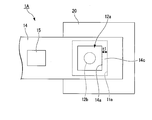
図1に示すように、金属片付き配線基板1Aは、フレキシブルプリント基板(FPC:Flexible Printed circuit)10Aと、フレキシブルプリント基板10Aの配線パターン12に接合された金属片20と、を備えている。
フレキシブルプリント基板10Aは、基材11と、配線パターン12と、カバーレイ(上側カバーレイ)14と、電子部品15と、を備えている。カバーレイ14は、フィルム(上側フィルム)13aと、フィルム13aに塗布された接着層(上側接着層)13bと、を有している。フレキシブルプリント基板10Aは、柔軟性に富んでおり、大きく撓ませた場合にも配線パターン12が機能するように構成されている。
フレキシブルプリント基板10Aは、基材11と、配線パターン12と、カバーレイ(上側カバーレイ)14と、電子部品15と、を備えている。カバーレイ14は、フィルム(上側フィルム)13aと、フィルム13aに塗布された接着層(上側接着層)13bと、を有している。フレキシブルプリント基板10Aは、柔軟性に富んでおり、大きく撓ませた場合にも配線パターン12が機能するように構成されている。
(方向定義)
本実施形態では、フレキシブルプリント基板10Aの厚さ方向を、単に厚さ方向という。また、厚さ方向に沿って、カバーレイ14側を上方といい、基材11側を下方という。また、厚さ方向から見ることを平面視という。
フレキシブルプリント基板10Aは、下方から上方に向かって、基材11、配線パターン12、カバーレイ14の順に積層された積層構造を有している。
本実施形態では、フレキシブルプリント基板10Aの厚さ方向を、単に厚さ方向という。また、厚さ方向に沿って、カバーレイ14側を上方といい、基材11側を下方という。また、厚さ方向から見ることを平面視という。
フレキシブルプリント基板10Aは、下方から上方に向かって、基材11、配線パターン12、カバーレイ14の順に積層された積層構造を有している。
電子部品15は、フレキシブルプリント基板10Aに実装されている。電子部品15としては、コンデンサ、抵抗、サーミスタ、IC、LED等が用いられる。また、他の回路基板を電子部品15としてフレキシブルプリント基板10Aに実装してもよい。
電子部品15の端子15aは、カバーレイ14に形成された実装用開口部14bを通じて、配線パターン12に電気的に接続されている。電子部品15の数は、1つであってもよいし、複数であってもよい。また、複数種類の電子部品15をフレキシブルプリント基板10Aに実装してもよい。
電子部品15の端子15aは、カバーレイ14に形成された実装用開口部14bを通じて、配線パターン12に電気的に接続されている。電子部品15の数は、1つであってもよいし、複数であってもよい。また、複数種類の電子部品15をフレキシブルプリント基板10Aに実装してもよい。
(基材)
基材11は、薄膜状に形成されており、フレキシブルプリント基板10Aの最下層に位置している。基材11としては、ポリイミドや液晶ポリマー等、可撓性および絶縁性のある材質を使用することができる。本実施形態では、基材11として、厚さ25μmのポリイミドフィルムが用いられている。基材11には、第1開口部11aが形成されている。図2に示すように、第1開口部11aは、平面視で正方形状に形成されている。本実施形態では、正方形状である第1開口部11aの一片の長さは7mmである。なお、第1開口部11aの形状および寸法は上記に限定されず、長方形、円形、楕円形などであってもよい。
基材11は、薄膜状に形成されており、フレキシブルプリント基板10Aの最下層に位置している。基材11としては、ポリイミドや液晶ポリマー等、可撓性および絶縁性のある材質を使用することができる。本実施形態では、基材11として、厚さ25μmのポリイミドフィルムが用いられている。基材11には、第1開口部11aが形成されている。図2に示すように、第1開口部11aは、平面視で正方形状に形成されている。本実施形態では、正方形状である第1開口部11aの一片の長さは7mmである。なお、第1開口部11aの形状および寸法は上記に限定されず、長方形、円形、楕円形などであってもよい。
(配線パターン)
配線パターン12は、基材11上に形成されている。配線パターン12の材質としては、例えば銅、ステンレス、アルミニウムなどの、導電性を有する金属の薄膜を用いることができる。本実施形態では、配線パターン12として、厚さ35μmの電解銅箔が用いられている。配線パターン12は、例えばサブトラクティブ法やセミアディティブ法などにより、基材11上に形成することができる。なお、配線パターン12と基材11との間には、両者を互いに接着する接着層が設けられていてもよい。
配線パターン12は、基材11上に形成されている。配線パターン12の材質としては、例えば銅、ステンレス、アルミニウムなどの、導電性を有する金属の薄膜を用いることができる。本実施形態では、配線パターン12として、厚さ35μmの電解銅箔が用いられている。配線パターン12は、例えばサブトラクティブ法やセミアディティブ法などにより、基材11上に形成することができる。なお、配線パターン12と基材11との間には、両者を互いに接着する接着層が設けられていてもよい。
配線パターン12は、基材11およびカバーレイ14に挟まれている。また、基材11には第1開口部11aが形成され、カバーレイ14には後述する第2開口部14aが形成されている。第1開口部11aおよび第2開口部14aは、平面視において、少なくとも一部が互いに重複している。このため、配線パターン12の少なくとも一部は、第1開口部11aおよび第2開口部14aを通して露出している。本実施形態では、配線パターン12のうち、第1開口部11aおよび第2開口部14aを通じて露出する部分を、露出部12aという。
露出部12aの一部は、下方に向けて(金属片20に向けて)撓むともに、金属片20に接合されている。露出部12aのうち、金属片20に接合された部分を、接合部12bという。本実施形態では、図2に示す平面視において、露出部12aは正方形状に形成され、接合部12bは円形状に形成されている。
(接着層)
接着層13bは、カバーレイ14のフィルム13aと配線パターン12とを互いに接着する。接着層13bの材質としては、エポキシ系、アクリル系、ポリイミド系等の、絶縁性および接着性を有する樹脂を用いることができる。本実施形態では、接着層13bとして、厚さ25μmのエポキシ系接着剤が用いられている。なお、接着層13bは、フィルム13aのうち第2開口部14aを除く部分の下面に設けられている。
接着層13bは、カバーレイ14のフィルム13aと配線パターン12とを互いに接着する。接着層13bの材質としては、エポキシ系、アクリル系、ポリイミド系等の、絶縁性および接着性を有する樹脂を用いることができる。本実施形態では、接着層13bとして、厚さ25μmのエポキシ系接着剤が用いられている。なお、接着層13bは、フィルム13aのうち第2開口部14aを除く部分の下面に設けられている。
(カバーレイ)
カバーレイ14は、配線パターン12を覆っており、フレキシブルプリント基板10Aの最上層に位置している。カバーレイ14のフィルム13aとしては、ポリイミド、液晶ポリマー等、可撓性および絶縁性のある材質を使用することができる。フィルム13aの材質は、基材11の材質と同じであってもよく、異なっていてもよい。本実施形態では、フィルム13aとして、基材11と同様の厚さ25μmのポリイミドフィルムが用いられている。接着層13bは、フィルム13aの下面に塗布されている。
カバーレイ14は、配線パターン12を覆っており、フレキシブルプリント基板10Aの最上層に位置している。カバーレイ14のフィルム13aとしては、ポリイミド、液晶ポリマー等、可撓性および絶縁性のある材質を使用することができる。フィルム13aの材質は、基材11の材質と同じであってもよく、異なっていてもよい。本実施形態では、フィルム13aとして、基材11と同様の厚さ25μmのポリイミドフィルムが用いられている。接着層13bは、フィルム13aの下面に塗布されている。
カバーレイ14には、第2開口部14aが形成されている。第2開口部14aは、カバーレイ14にレーザー加工、金型加工、NC加工(Numerical Control machining)などを施すことで形成することができる。なお、配線パターン12は、第2開口部14aを通じて上方に露出している。
図2に示すように、第2開口部14aは、平面視において、第1開口部11aよりも小さく、第1開口部11aと重なる位置に形成されている。第2開口部14aは、平面視で正方形状に形成されている。本実施形態では、正方形である第2開口部14aの一片の長さは6mmであり、平面視において、第1開口部11a(一片7mmの正方形)と図心の位置が略一致している。このため、カバーレイ14は、第2開口部14aの開口縁に沿って、0.5mmの幅で第1開口部11aにオーバーラップしている。カバーレイ14のうち、第1開口部11aにオーバーラップしている部分をオーバーラップ部14cという。また、平面視におけるオーバーラップ部14cの幅を、オーバーラップ量t1という。換言すると、オーバーラップ量t1は、オーバーラップ部14cにおける、第1開口部11aおよび第2開口部14aの開口縁同士の間の距離である。
本実施形態では、オーバーラップ部14cは、平面視において、幅が0.5mmの正方形の枠状に形成されている。また、オーバーラップ部14cの幅(オーバーラップ量t1)は、第1開口部11aの開口縁に沿って略均一となっている。
なお、第2開口部14aの形状および寸法は特に限定されず、長方形、円形、楕円形などであってもよい。また、平面視において、第2開口部14aの図心の位置は、第1開口部11aの図心の位置に一致していなくてもよい。すなわち、オーバーラップ部14cの形状は特に限定されず、オーバーラップ量t1が第2開口部14aの開口縁に沿って不均一であってもよい。ただし、カバーレイ14の少なくとも一部が第1開口部11aを覆っており、オーバーラップ部14cが形成されていることが好ましい。また、オーバーラップ量t1は、部分的に0mmであってもよいが、少なくとも一部において0.1mm以上であることが好ましい。詳細は後述するが、オーバーラップ量t1が大きいほど、オーバーラップ部14cが下方に向けて撓みやすくなり、配線パターン12に作用する応力・張力などを低減することができる。
(金属片)
金属片20は、アルミニウムなどの金属によって、膜状、棒状、あるいは板状に形成されている。なお、金属片20の材質、形状は適宜変更してもよい。本実施形態では、金属片20として、厚さが1mmの板状のアルミニウム(A1050)が用いられている。
金属片20は、基材11の第1開口部11aを下方から覆っている。図示の例では、金属片20が第1開口部11aの全体を覆っているが、少なくとも一部を覆っていればよい。金属片20は、配線パターン12の接合部12bに接合されており、配線パターン12に電気的に接続されている。
金属片20は、アルミニウムなどの金属によって、膜状、棒状、あるいは板状に形成されている。なお、金属片20の材質、形状は適宜変更してもよい。本実施形態では、金属片20として、厚さが1mmの板状のアルミニウム(A1050)が用いられている。
金属片20は、基材11の第1開口部11aを下方から覆っている。図示の例では、金属片20が第1開口部11aの全体を覆っているが、少なくとも一部を覆っていればよい。金属片20は、配線パターン12の接合部12bに接合されており、配線パターン12に電気的に接続されている。
(製造方法)
次に、以上のような構成を有する金属片付き配線基板1Aの製造方法の一例について、図3を用いて説明する。
次に、以上のような構成を有する金属片付き配線基板1Aの製造方法の一例について、図3を用いて説明する。
(準備工程)
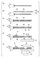
まず、フレキシブルプリント基板10Aを用意する準備工程が行われる。準備工程では、図3の(a)に示すように、基材11上に配線パターン12が形成されたシートSを用意する。
次に、図3の(b)に示すように、第2開口部14aおよび実装用開口部14bが形成されたカバーレイ14を、シートSの配線パターン12に対向させる。このとき、カバーレイ14のフィルム13aの下面には、接着層13bとなる半硬化状態の接着剤が塗布されている。
まず、フレキシブルプリント基板10Aを用意する準備工程が行われる。準備工程では、図3の(a)に示すように、基材11上に配線パターン12が形成されたシートSを用意する。
次に、図3の(b)に示すように、第2開口部14aおよび実装用開口部14bが形成されたカバーレイ14を、シートSの配線パターン12に対向させる。このとき、カバーレイ14のフィルム13aの下面には、接着層13bとなる半硬化状態の接着剤が塗布されている。
次に、カバーレイ14およびシートSを位置合わせする。位置合わせの方法としては、位置決めピンを用いたり、画像処理による位置制御装置を用いたりすることができる。
次に、図3の(c)に示すように、カバーレイ14をシートS上に積層し、加熱プレスにより一体化させる。加熱プレスは、例えば温度100~200℃、圧力0.1~10MPa、加圧時間1~120分の範囲が好ましい。さらに、必要に応じて、上記加熱プレス後にオーブンにて加熱してもよい。
次に、図3の(c)に示すように、カバーレイ14をシートS上に積層し、加熱プレスにより一体化させる。加熱プレスは、例えば温度100~200℃、圧力0.1~10MPa、加圧時間1~120分の範囲が好ましい。さらに、必要に応じて、上記加熱プレス後にオーブンにて加熱してもよい。
次に、図3の(d)に示すように、基材11を部分的に除去し、第1開口部11aを形成する。除去方法としては、レーザー加工、エッチング加工等を用いることができる。基材11に第1開口部11aが形成されることで、配線パターン12が部分的に露出する。このとき、第1開口部11aは、カバーレイ14が寸法tだけオーバーラップするように、第2開口部14aよりも大きく形成する。第1開口部11aを形成することで、配線パターン12の露出部12aが下方に露出する。
次に、図3の(e)に示すように、フレキシブルプリント基板10Aに電子部品15を実装する。実装方法としては、はんだ、銀ペースト、超音波接合、ワイヤーボンド等を用いることができる。
次に、金属片20をフレキシブルプリント基板10Aの下方に位置させて、金属片20が厚さ方向で露出部12aに対向するように配置する。
次に、金属片20をフレキシブルプリント基板10Aの下方に位置させて、金属片20が厚さ方向で露出部12aに対向するように配置する。
(変形工程)
次に、図3の(f)に示すように、配線パターン12の露出部12aを金属片20に向けて変形させる変形工程が行われる。変形工程では、金属片20とフレキシブルプリント基板10Aとを位置決めし、後述の接合工程で用いられる接合工具K1を、第2開口部14aを通じて露出部12aに押し当てる。これにより、露出部12aが第1開口部11aを通じて下方に伸びるように変形し、金属片20に接触する。このとき、カバーレイ14のオーバーラップ部14cも下方に向けて撓む。
次に、図3の(f)に示すように、配線パターン12の露出部12aを金属片20に向けて変形させる変形工程が行われる。変形工程では、金属片20とフレキシブルプリント基板10Aとを位置決めし、後述の接合工程で用いられる接合工具K1を、第2開口部14aを通じて露出部12aに押し当てる。これにより、露出部12aが第1開口部11aを通じて下方に伸びるように変形し、金属片20に接触する。このとき、カバーレイ14のオーバーラップ部14cも下方に向けて撓む。
(接合工程)
次に、配線パターン12と金属片20とを接合する接合工程が行われる。本実施形態では、ダイレクト通電方式の抵抗溶接機を採用した場合について説明する。抵抗溶接の場合、接合工具K1、K2として溶接電極が用いられる。接合工具K1は、露出部12aに上方から接触し、露出部12aを通じて金属片20に電気的に接続された状態とされる。接合工具K2は、平面視で接合工具K1と重なる位置において、金属片20に下方から接触している。つまり、一対の接合工具K1,K2は、露出部12aおよび金属片20を厚さ方向で挟んだ状態となる。
次に、配線パターン12と金属片20とを接合する接合工程が行われる。本実施形態では、ダイレクト通電方式の抵抗溶接機を採用した場合について説明する。抵抗溶接の場合、接合工具K1、K2として溶接電極が用いられる。接合工具K1は、露出部12aに上方から接触し、露出部12aを通じて金属片20に電気的に接続された状態とされる。接合工具K2は、平面視で接合工具K1と重なる位置において、金属片20に下方から接触している。つまり、一対の接合工具K1,K2は、露出部12aおよび金属片20を厚さ方向で挟んだ状態となる。
次に、接合工具K1、K2を金属片20に向けて加圧した状態で、接合工具K1,K2に電圧を加え、電流を流す。電流の方向は任意であり、接合工具K1から接合工具K2に向かってもよく、その逆であってもよい。また、接合工具K1,K2の間で、所定の時間間隔で交互に電流の向きが変わってもよい。本実施形態における溶接条件は、電流2kA、溶接時間10ミリ秒、加圧力16kgfである。一対の接合工具K1、K2間で電流が流れると、配線パターン12と金属片20との界面で接触抵抗による熱が発生する。この熱により、配線パターン12または金属片20が溶融し、これらを溶接(接合)することができる。接合工具K1の先端が円形状である場合には、接合部12bは平面視で円形状に形成される。なお、接合工程において抵抗溶接を採用した場合には、接合部12bにおける金属片20との界面に溶融部(ナゲット)および合金層を形成することができる。なお、ナゲットとは熱によって溶融した後、再び凝固した部分である。
なお、上記接合工程では、パラレル通電方式の抵抗溶接機を用いてもよい。この場合、図示は省略するが、接合工具K2は、接合工具K1に対して平面視で所定の間隔を空けて、金属片20に上方または下方から接触した状態とされる。
ところで、上記変形工程において、仮にカバーレイ14がオーバーラップ部14cを有していない場合には、第1開口部11aの開口縁に配線パターン12が強く押し付けられ、配線パターン12に局所的に大きな応力が生じ得る。そして、この応力によって配線パターン12が破断してしまうおそれがある。
これに対して本実施形態では、カバーレイ14が第1開口部11aを部分的に覆っている。このため、露出部12aが下方に向けて押圧されると、カバーレイ14のオーバーラップ部14cも下方に向けて撓む。これにより、配線パターン12に局所的に大きな応力が作用することが抑えられる。また、局所的な応力によって配線パターン12が破断することを抑えることができる。
なお、オーバーラップ量t1が大きいほど、オーバーラップ部14cが緩やかに(大きい曲率半径で)下方に向けて撓む。従って、配線パターン12の破断をより確実に抑えることができる。好ましいオーバーラップ量t1は、カバーレイ14のフィルム13aの材質や厚みによるが、例えば0.5mm以上であるとよい。
以上説明したように、本実施形態によれば、平面視において、第2開口部14aの少なくとも一部が第1開口部11aに重なっており、金属片20が第1開口部11aの少なくとも一部を下方から覆っている。このため、第2開口部14aを通じて接合工具K1を配線パターン12の露出部12aに押し当て、第1開口部11aを通るように露出部12aを変形させ、露出部12aと金属片20とを接触させることができる。そして、その状態のまま露出部12aと金属片20との接合を行うことができる。このように、変形工程と接合工程とを略同時に行うことができるため、製造効率を向上させることができる。
また、カバーレイ14は、接着層13bによって配線パターン12に接着され、カバーレイ14の一部が平面視で第1開口部11aに重なっている。従って、上記のように露出部12aを変形させた際、カバーレイ14のオーバーラップ部14cを下方に向けて撓ませることができる。これにより、配線パターン12に局所的に大きな応力が作用することが抑えられる。従って、配線パターン12の断線が発生することが抑えられる。
なお、本発明の技術的範囲は前記実施の形態に限定されるものではなく、本発明の趣旨を逸脱しない範囲において種々の変更を加えることが可能である。
例えば、前記実施形態では、第1開口部11aおよび第2開口部14aが、互いに略相似かつ図心が一致した状態で配置されている。しかしながら、第1開口部11aおよび第2開口部14aの図心の位置は、平面視においてずれていてもよい。また、第1開口部11aおよび第2開口部14aの形状は互いに略相似でなくてもよい。
また、前記実施形態では、抵抗溶接を用いて配線パターン12と金属片20とを接合する場合について説明したが、接合の方法は適宜変更してもよい。例えば、接合工程において、超音波接合やレーザー接合などを採用してもよい。
接合工程で超音波接合を用いる場合、図4に示すように、接合工具K1、K2としてホーンおよびアンビルを用いる。そして、ホーンおよびアンビルによって配線パターン12および金属片20を挟んで加圧する。これにより、前記実施形態と同様に、加圧時に配線パターン12が変形して、金属片20に接触する(変形工程)。この状態でホーンが軸方向に振動すると、振動が配線パターン12および金属片20に伝わり、両者の接触面で摩擦熱が生じる。この摩擦熱などにより、配線パターン12と金属片20とが拡散接合(熱圧着)され、あるいは冶金接合される。これにより、両者を接合することができる(接合工程)。なお、変形工程および接合工程において、フレキシブルプリント基板10Aと金属片20の上下関係は逆であってもよい。超音波接合を用いた場合、比較的低温で配線パターン12と金属片20とを接合することができる。
(第2実施形態)
次に、本発明に係る第2実施形態について説明するが、第1実施形態と基本的な構成は同様である。このため、同様の構成には同一の符号を付してその説明は省略し、異なる点についてのみ説明する。
本実施形態では、第1実施形態における基材11が、下側カバーレイ17に置き換わっている。
次に、本発明に係る第2実施形態について説明するが、第1実施形態と基本的な構成は同様である。このため、同様の構成には同一の符号を付してその説明は省略し、異なる点についてのみ説明する。
本実施形態では、第1実施形態における基材11が、下側カバーレイ17に置き換わっている。
図5に示すように、本実施形態の金属片付き配線基板1Bは、フレキシブルプリント基板10Bと、フレキシブルプリント基板10Bの配線パターン12に接合された金属片20と、を備えている。
フレキシブルプリント基板10Bは、配線パターン12と、上側カバーレイ14と、下側カバーレイ17と、電子部品15と、を備えている。上側カバーレイ14は、フィルム(上側フィルム)13aと、フィルム13aに塗布された接着層(上側接着層)13bと、を有している。下側カバーレイ17は、フィルム(下側フィルム)16aと、フィルム16aに塗布された接着層(下側接着層)16bと、を有している。フレキシブルプリント基板10Bは、柔軟性に富んでおり、大きく撓ませた場合にも配線パターン12が機能するように構成されている。
フレキシブルプリント基板10Bは、配線パターン12と、上側カバーレイ14と、下側カバーレイ17と、電子部品15と、を備えている。上側カバーレイ14は、フィルム(上側フィルム)13aと、フィルム13aに塗布された接着層(上側接着層)13bと、を有している。下側カバーレイ17は、フィルム(下側フィルム)16aと、フィルム16aに塗布された接着層(下側接着層)16bと、を有している。フレキシブルプリント基板10Bは、柔軟性に富んでおり、大きく撓ませた場合にも配線パターン12が機能するように構成されている。
下側フィルム16aとしては、第1実施形態で説明した上側フィルム13aと同様の材質を用いることができる。なお、下側フィルム16aと上側フィルム13aとで異なる材質を用いてもよい。
下側接着層16bとしては、第1実施形態で説明した上側接着層13bと同様の材質を用いることができる。なお、下側接着層16bと上側接着層13bとで異なる材質を用いてもよい。
下側接着層16bとしては、第1実施形態で説明した上側接着層13bと同様の材質を用いることができる。なお、下側接着層16bと上側接着層13bとで異なる材質を用いてもよい。
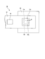
下側カバーレイ17には第1開口部17aが形成され、上側カバーレイ14には第2開口部14aが形成されている。図6に示すように、第1開口部17aは、平面視において、第2開口部14aよりも小さい正方形状に形成されている。本実施形態では、第1開口部17aが一片6mmの正方形状であり、第2開口部14aが一片7mmの正方形状であり、第1開口部17aおよび第2開口部14aの図心の位置が平面視で一致している。このため、断面視(図5)で第1開口部17aが第2開口部14aの内側に突出しており、突出量t2が0.5mmとなっている。また、突出量t2は、第1開口部17aの開口縁に沿って略均一となっている。突出量t2は、第1開口部17aおよび第2開口部14aの開口縁同士の間の距離である。平面視(図6)において、第1開口部17aは、第2開口部14aの内側に位置している。
なお、第1実施形態と同様に、第1開口部17aおよび第2開口部14aの位置、形状、大きさなどは適宜変更してもよい。ただし、突出量t2は、0.1mm以上であることが好ましい。
(製造方法)
次に、以上のような構成を有する金属片付き配線基板1Bの製造方法の一例について、図7の(a)~(f)を用いて説明する。なお、第1実施形態と同様の内容については説明を省略する。
次に、以上のような構成を有する金属片付き配線基板1Bの製造方法の一例について、図7の(a)~(f)を用いて説明する。なお、第1実施形態と同様の内容については説明を省略する。
(準備工程)
まず、フレキシブルプリント基板10Bを用意する準備工程が行われる。準備工程では、図7の(a)に示すように、配線パターン12となる金属箔を、上側カバーレイ14に対向させる。このとき、上側カバーレイ14には、予め第2開口部14aを形成しておく。
まず、フレキシブルプリント基板10Bを用意する準備工程が行われる。準備工程では、図7の(a)に示すように、配線パターン12となる金属箔を、上側カバーレイ14に対向させる。このとき、上側カバーレイ14には、予め第2開口部14aを形成しておく。
本実施形態では、フィルム13a、16aとして厚さ25μmのポリイミドフィルム(線膨張係数:27ppm/K、ヤング率:3.5GPa)を用い、接着層13b、16bとして厚さ25μmのエポキシ系接着剤(線膨張係数:60ppm/K、ヤング率:0.4GPa)を用いた。接着層13b、16bのヤング率は、フィルム13a、16aのヤング率よりも低いことが好ましい。具体的には、接着層13b、16bのヤング率は、3GPa以下が好ましく、1GPa以下がより好ましく、0.5GPa以下が更に好ましい。
次に、図7の(b)に示すように、上側カバーレイ14と金属箔とを位置合わせして一体化する。次に、図7の(c)に示すように、金属箔を加工して配線パターン12を得る。
次に、図7の(d)に示すように、第1開口部17aが形成された下側カバーレイ17を、配線パターン12の下面に対向させる。第1開口部17aの大きさは、第2開口部14aよりも小さくし、突出量t2が所望の大きさになるようにする。
次に、図7の(d)に示すように、第1開口部17aが形成された下側カバーレイ17を、配線パターン12の下面に対向させる。第1開口部17aの大きさは、第2開口部14aよりも小さくし、突出量t2が所望の大きさになるようにする。
次に、図7の(e)に示すように、上側カバーレイ14および下側カバーレイ17の接着層13b、16b同士を、配線パターン12を挟んで貼り合わせ、上側カバーレイ14に電子部品15を実装する。これにより、フレキシブルプリント基板10Bが得られる。
そして、第1実施形態と同様の変形工程および接合工程を行うことで、図7の(f)に示すような金属片付き配線基板1Bが得られる。
そして、第1実施形態と同様の変形工程および接合工程を行うことで、図7の(f)に示すような金属片付き配線基板1Bが得られる。
ここで、変形工程において配線パターン12を変形させる際に、配線パターン12は第1開口部17aのエッジに押し付けられる。このとき、図8に示すように、下側接着層16bが配線パターン12によって下方に押されて変形し、下側接着層16bの開口縁に、上方に向けて凸の曲面16b1が形成される。このため、配線パターン12は曲面16b1に沿って金属片20に向けて変形することになり、変形の開始位置に大きな応力が作用することが抑えられる。
次に、金属片付き配線基板1Bの作用について説明する。
サーマルサイクル試験のような温度変化が金属片付き配線基板1Bに加わった場合、各部材間の接触面には、線膨張係数の差に起因する応力が作用する。このとき、フィルム13a、16aは、弾性率が比較的高く変形しにくいため、接触面における応力を自身の変形に変えることが難しく、そのために他の部材との界面で剥離を生じやすい。そこで本実施形態では、配線パターン12とフィルム13a、16aとの間に、弾性率が小さく変形し易い接着層13b、16bが配置されている。この構成により、接着層13b、16bが緩衝材となり、配線パターン12に大きな応力が作用してしまうことを抑えることができる。従って、温度変化が繰り返されたとしても、配線パターン12の表面で剥離が生じたり、配線パターン12に大きな熱応力が加わったりすることが抑えられる。
サーマルサイクル試験のような温度変化が金属片付き配線基板1Bに加わった場合、各部材間の接触面には、線膨張係数の差に起因する応力が作用する。このとき、フィルム13a、16aは、弾性率が比較的高く変形しにくいため、接触面における応力を自身の変形に変えることが難しく、そのために他の部材との界面で剥離を生じやすい。そこで本実施形態では、配線パターン12とフィルム13a、16aとの間に、弾性率が小さく変形し易い接着層13b、16bが配置されている。この構成により、接着層13b、16bが緩衝材となり、配線パターン12に大きな応力が作用してしまうことを抑えることができる。従って、温度変化が繰り返されたとしても、配線パターン12の表面で剥離が生じたり、配線パターン12に大きな熱応力が加わったりすることが抑えられる。
また、本実施形態では、下側カバーレイ17が、配線パターン12に接する下側接着層16bと、下側接着層16bによって配線パターン12に接着された下側フィルム16aと、を有している。そして平面視において、第1開口部17aの少なくとも一部が第2開口部14aの内側に位置している。この構成により、配線パターン12が第1開口部17aの内部に向けて変形する際に、下側フィルム16aのエッジと配線パターン12との間に介在する下側接着層16bによって、配線パターン12が破れたり折れたりすることが抑えられる。従って、配線パターン12の断線の発生を抑えることができる。
また、下側フィルム16aと比較して下側接着層16bの弾性率が小さく、下側接着層16bが変形しやすいため、より確実に配線パターン12の断線の発生を抑えることができる。また、下側接着層16bの開口縁に曲面16b1が形成されることで、配線パターン12の変形の開始位置に大きな応力が作用することが抑えられる。
また、上側カバーレイ14は、配線パターン12に接する上側接着層13bと、上側接着層13bによって配線パターン12に接着された上側フィルム13aと、を有している。このように、配線パターン12が、比較的弾性率の低い2つの接着層13b、16bにより挟まれている。このため、温度変化などによって上側フィルム13aまたは下側フィルム16aが配線パターン12よりも大きく伸縮した場合でも、フィルム13a、16aと配線パターン12との間に位置する接着層13b、16bが緩衝材となり、配線パターン12に作用する熱応力を低減することができる。
また、フレキシブルプリント基板10Bは、配線パターン12を中心として上下対称な積層順序を有している。このため、温度変化などによる各部材の変形量が、配線パターン12の上側と下側とで実質的に同等になる。従って、配線パターン12に作用する熱応力をより低減することができる。なお、接着層13b、16b同士およびフィルム13a、16a同士は、互いに同一の材質により形成されていることが好ましい。この場合、配線パターン12の上側と下側とで変形量をより確実に一致させることができる。
なお、本発明の趣旨を逸脱しない範囲で、上記した実施の形態における構成要素を周知の構成要素に置き換えることは適宜可能であり、また、上記した実施形態や変形例を適宜組み合わせてもよい。
例えば、第1実施形態のフレキシブルプリント基板10Aが、配線パターン12を中心として上下対称な積層順序を有してもよい。この場合、基材11と配線パターン12との間に、接着層が設けられていてもよい。
例えば、第1実施形態のフレキシブルプリント基板10Aが、配線パターン12を中心として上下対称な積層順序を有してもよい。この場合、基材11と配線パターン12との間に、接着層が設けられていてもよい。
1A、1B…金属片付き配線基板 10A、10B…フレキシブルプリント基板 11…基材 11a…第1開口部 12…配線パターン 13a…フィルム(上側フィルム) 13b…接着層(上側接着層) 14…カバーレイ(上側カバーレイ) 14a…第2開口部 16a…フィルム(下側フィルム) 16b…接着層(下側接着層) 17…カバーレイ(下側カバーレイ) 17a…第1開口部 K1~K2…接合工具
Claims (6)
- 第1開口部を有する基材と、前記基材上に形成された配線パターンと、接着層によって前記配線パターンに接着され、かつ第2開口部を有するカバーレイと、を有するフレキシブルプリント基板と、
前記第1開口部の少なくとも一部を下方から覆う金属片と、を備え、
前記配線パターンは、前記第1開口部を通じて前記金属片に接触し、かつ前記金属片に接合され、
前記第2開口部の少なくとも一部が平面視で前記第1開口部に重なり、かつ前記カバーレイの一部が平面視で前記第1開口部に重なっている、金属片付き配線基板。 - 第1開口部を有する下側カバーレイと、第2開口部を有する上側カバーレイと、前記下側カバーレイと前記上側カバーレイとの間に配置された配線パターンと、を有するフレキシブルプリント基板と、
前記第1開口部の少なくとも一部を下方から覆う金属片と、を備え、
前記配線パターンは、前記第1開口部を通じて前記金属片に接触し、かつ前記金属片に接合され、
前記下側カバーレイは、前記配線パターンに接する下側接着層と、前記下側接着層によって前記配線パターンに接着された下側フィルムと、を有し、
前記第1開口部の少なくとも一部が平面視で前記第2開口部の内側に位置している、金属片付き配線基板。 - 前記下側フィルムの弾性率よりも前記下側接着層の弾性率が小さい、請求項2に記載の金属片付き配線基板。
- 前記上側カバーレイは、前記配線パターンに接する上側接着層と、前記上側接着層によって前記配線パターンに接着された上側フィルムと、を有する、請求項2または3に記載の金属片付き配線基板。
- 前記フレキシブルプリント基板の積層順序が、前記配線パターンを中心として上下対称である、請求項1から4のいずれか1項に記載の金属片付き配線基板。
- 第1開口部が形成された基材と、第2開口部が形成されたカバーレイと、前記基材および前記カバーレイによって挟まれた配線パターンと、を有するフレキシブルプリント基板を用意する準備工程と、
前記第2開口部を通じて接合工具を前記配線パターンに押し当て、前記配線パターンを金属片に向けて変形させる変形工程と、
前記接合工具を用いて前記配線パターンと前記金属片とを接合させる接合工程と、を有する、金属片付き配線基板の製造方法。
Priority Applications (4)
| Application Number | Priority Date | Filing Date | Title |
|---|---|---|---|
| KR1020207024210A KR20200110421A (ko) | 2017-12-28 | 2019-02-12 | 금속편 부착 배선 기판 및 금속편 부착 배선 기판의 제조 방법 |
| DE112019001056.5T DE112019001056T5 (de) | 2017-12-28 | 2019-02-12 | Leiterplatte mit metallstück und verfahren zur herstellung einer leiterplatte mit metallstück |
| CN201980013961.7A CN111742623A (zh) | 2017-12-28 | 2019-02-12 | 带金属片配线基板以及带金属片配线基板的制造方法 |
| US16/975,937 US20200404789A1 (en) | 2017-12-28 | 2019-02-12 | Wiring board including metal piece and method for manufacturing wiring board including metal piece |
Applications Claiming Priority (3)
| Application Number | Priority Date | Filing Date | Title |
|---|---|---|---|
| JP2017252731 | 2017-12-28 | ||
| JP2018034916A JP2019121774A (ja) | 2017-12-28 | 2018-02-28 | 金属片付き配線基板および金属片付き配線基板の製造方法 |
| JP2018-034916 | 2018-02-28 |
Publications (1)
| Publication Number | Publication Date |
|---|---|
| WO2019167602A1 true WO2019167602A1 (ja) | 2019-09-06 |
Family
ID=67306611
Family Applications (1)
| Application Number | Title | Priority Date | Filing Date |
|---|---|---|---|
| PCT/JP2019/004813 Ceased WO2019167602A1 (ja) | 2017-12-28 | 2019-02-12 | 金属片付き配線基板および金属片付き配線基板の製造方法 |
Country Status (6)
| Country | Link |
|---|---|
| US (1) | US20200404789A1 (ja) |
| JP (1) | JP2019121774A (ja) |
| KR (1) | KR20200110421A (ja) |
| CN (1) | CN111742623A (ja) |
| DE (1) | DE112019001056T5 (ja) |
| WO (1) | WO2019167602A1 (ja) |
Families Citing this family (1)
| Publication number | Priority date | Publication date | Assignee | Title |
|---|---|---|---|---|
| DE102022213610A1 (de) | 2022-12-14 | 2024-06-20 | Robert Bosch Gesellschaft mit beschränkter Haftung | Kontaktierung einer flexiblen Leiterfolie mit einer starren Leiterplatte sowie Verfahren zur Herstellung einer derartigen Kontaktierung |
Citations (4)
| Publication number | Priority date | Publication date | Assignee | Title |
|---|---|---|---|---|
| JPH0535589B2 (ja) * | 1985-06-22 | 1993-05-26 | Nippon Mekutoron Kk | |
| JPH0685439A (ja) * | 1992-09-01 | 1994-03-25 | Nitto Denko Corp | フレキシブルプリント基板 |
| DE102005035102A1 (de) * | 2005-07-27 | 2007-02-01 | Robert Bosch Gmbh | Elektrisch leitende Verbindung und Verfahren zum Herstellen einer solchen |
| JP2013222480A (ja) * | 2012-04-16 | 2013-10-28 | Dainippon Printing Co Ltd | サスペンション用基板、サスペンション、ヘッド付サスペンション、ヘッド付サスペンションと外部接続基板との組合体およびハードディスクドライブ |
Family Cites Families (13)
| Publication number | Priority date | Publication date | Assignee | Title |
|---|---|---|---|---|
| DE69732389T2 (de) * | 1996-04-12 | 2005-12-22 | Canon K.K. | Tintenstrahldruckkopfherstellungsverfahren |
| JP2000307202A (ja) | 1999-04-22 | 2000-11-02 | Sumitomo Wiring Syst Ltd | 回路板および該回路板を収容した電気接続箱 |
| JP3205548B2 (ja) * | 1999-10-01 | 2001-09-04 | ソニーケミカル株式会社 | 多層フレキシブル配線板 |
| WO2006011404A1 (ja) * | 2004-07-27 | 2006-02-02 | Kaneka Corporation | 接着フィルムおよびその利用 |
| US8101868B2 (en) * | 2005-10-14 | 2012-01-24 | Ibiden Co., Ltd. | Multilayered printed circuit board and method for manufacturing the same |
| JP2011159456A (ja) * | 2010-01-29 | 2011-08-18 | Fujikura Ltd | スイッチモジュール |
| JP2011198728A (ja) * | 2010-03-24 | 2011-10-06 | Fujikura Ltd | スイッチモジュール |
| JP2011211099A (ja) * | 2010-03-30 | 2011-10-20 | Tdk Corp | 電子部品内蔵基板及び電子部品内蔵基板の製造方法 |
| JP2012146353A (ja) * | 2011-01-07 | 2012-08-02 | Sumitomo Electric Printed Circuit Inc | フレキシブル配線板、配線板の接続構造、およびこれらの製造方法 |
| JP2012164952A (ja) * | 2011-01-20 | 2012-08-30 | Ibiden Co Ltd | 電子部品内蔵配線板及びその製造方法 |
| JP5084944B1 (ja) * | 2011-11-28 | 2012-11-28 | 日東電工株式会社 | 配線回路基板 |
| JP5882132B2 (ja) * | 2012-05-14 | 2016-03-09 | 日本メクトロン株式会社 | フレキシブル回路基板及びその製造方法 |
| US9844146B2 (en) * | 2016-05-11 | 2017-12-12 | Flextronics Automotive Gmbh & Co. Kg | Electrical circuitry assembly and method for manufacturing the same |
-
2018
- 2018-02-28 JP JP2018034916A patent/JP2019121774A/ja not_active Ceased
-
2019
- 2019-02-12 KR KR1020207024210A patent/KR20200110421A/ko not_active Ceased
- 2019-02-12 US US16/975,937 patent/US20200404789A1/en not_active Abandoned
- 2019-02-12 DE DE112019001056.5T patent/DE112019001056T5/de not_active Withdrawn
- 2019-02-12 WO PCT/JP2019/004813 patent/WO2019167602A1/ja not_active Ceased
- 2019-02-12 CN CN201980013961.7A patent/CN111742623A/zh active Pending
Patent Citations (4)
| Publication number | Priority date | Publication date | Assignee | Title |
|---|---|---|---|---|
| JPH0535589B2 (ja) * | 1985-06-22 | 1993-05-26 | Nippon Mekutoron Kk | |
| JPH0685439A (ja) * | 1992-09-01 | 1994-03-25 | Nitto Denko Corp | フレキシブルプリント基板 |
| DE102005035102A1 (de) * | 2005-07-27 | 2007-02-01 | Robert Bosch Gmbh | Elektrisch leitende Verbindung und Verfahren zum Herstellen einer solchen |
| JP2013222480A (ja) * | 2012-04-16 | 2013-10-28 | Dainippon Printing Co Ltd | サスペンション用基板、サスペンション、ヘッド付サスペンション、ヘッド付サスペンションと外部接続基板との組合体およびハードディスクドライブ |
Also Published As
| Publication number | Publication date |
|---|---|
| US20200404789A1 (en) | 2020-12-24 |
| JP2019121774A (ja) | 2019-07-22 |
| CN111742623A (zh) | 2020-10-02 |
| KR20200110421A (ko) | 2020-09-23 |
| DE112019001056T5 (de) | 2020-11-12 |
Similar Documents
| Publication | Publication Date | Title |
|---|---|---|
| JP6103054B2 (ja) | 樹脂多層基板の製造方法 | |
| US7080445B2 (en) | Method for connecting printed circuit boards and connected printed circuit boards | |
| JP6672108B2 (ja) | 配線基板及び当該配線基板の製造方法 | |
| JP5644286B2 (ja) | 電子部品の表面実装方法及び電子部品が実装された基板 | |
| JP2014146650A (ja) | 配線基板およびその製造方法 | |
| JPWO2009107342A1 (ja) | 電子部品モジュールの製造方法 | |
| US20200404789A1 (en) | Wiring board including metal piece and method for manufacturing wiring board including metal piece | |
| JP2006165079A (ja) | フレキシブルプリント基板 | |
| CN100587901C (zh) | 电子部件及其制造方法 | |
| JP2011171571A (ja) | プリント配線基板及びその製造方法 | |
| JP4657840B2 (ja) | 半導体装置、およびその製造方法 | |
| JP5423246B2 (ja) | 基板モジュールおよびその製造方法 | |
| JP2022170645A (ja) | スイッチ | |
| JP3948250B2 (ja) | プリント配線基板の接続方法 | |
| JP6348759B2 (ja) | 半導体モジュール、接合用治具、および半導体モジュールの製造方法 | |
| JP5609452B2 (ja) | 複合基板の製造方法 | |
| JP2019041019A (ja) | プリント配線板およびその製造方法 | |
| JP2005217030A (ja) | リジットフレックス基板及びその製造方法並びに補修方法 | |
| JP4755151B2 (ja) | 電気接続装置 | |
| JP3136149U (ja) | 貼り合わせ式条状ランプ装置 | |
| JP2020155537A (ja) | 金属片付き配線基板 | |
| JP2015204446A5 (ja) | ||
| JP6089614B2 (ja) | 樹脂多層基板 | |
| JPWO2017187939A1 (ja) | 樹脂多層基板およびその製造方法 | |
| JP2006107748A (ja) | 補強板付fpcとicパッケージの実装方法 |
Legal Events
| Date | Code | Title | Description |
|---|---|---|---|
| 121 | Ep: the epo has been informed by wipo that ep was designated in this application |
Ref document number: 19760308 Country of ref document: EP Kind code of ref document: A1 |
|
| ENP | Entry into the national phase |
Ref document number: 20207024210 Country of ref document: KR Kind code of ref document: A |
|
| 122 | Ep: pct application non-entry in european phase |
Ref document number: 19760308 Country of ref document: EP Kind code of ref document: A1 |