WO2019130395A1 - 電力変換装置 - Google Patents
電力変換装置 Download PDFInfo
- Publication number
- WO2019130395A1 WO2019130395A1 PCT/JP2017/046449 JP2017046449W WO2019130395A1 WO 2019130395 A1 WO2019130395 A1 WO 2019130395A1 JP 2017046449 W JP2017046449 W JP 2017046449W WO 2019130395 A1 WO2019130395 A1 WO 2019130395A1
- Authority
- WO
- WIPO (PCT)
- Prior art keywords
- semiconductor element
- control
- pulse width
- semiconductor device
- leg
- Prior art date
Links
Images


Classifications
-
- H—ELECTRICITY
- H02—GENERATION; CONVERSION OR DISTRIBUTION OF ELECTRIC POWER
- H02M—APPARATUS FOR CONVERSION BETWEEN AC AND AC, BETWEEN AC AND DC, OR BETWEEN DC AND DC, AND FOR USE WITH MAINS OR SIMILAR POWER SUPPLY SYSTEMS; CONVERSION OF DC OR AC INPUT POWER INTO SURGE OUTPUT POWER; CONTROL OR REGULATION THEREOF
- H02M7/00—Conversion of ac power input into dc power output; Conversion of dc power input into ac power output
- H02M7/02—Conversion of ac power input into dc power output without possibility of reversal
- H02M7/04—Conversion of ac power input into dc power output without possibility of reversal by static converters
- H02M7/12—Conversion of ac power input into dc power output without possibility of reversal by static converters using discharge tubes with control electrode or semiconductor devices with control electrode
- H02M7/21—Conversion of ac power input into dc power output without possibility of reversal by static converters using discharge tubes with control electrode or semiconductor devices with control electrode using devices of a triode or transistor type requiring continuous application of a control signal
- H02M7/217—Conversion of ac power input into dc power output without possibility of reversal by static converters using discharge tubes with control electrode or semiconductor devices with control electrode using devices of a triode or transistor type requiring continuous application of a control signal using semiconductor devices only
-
- H—ELECTRICITY
- H02—GENERATION; CONVERSION OR DISTRIBUTION OF ELECTRIC POWER
- H02M—APPARATUS FOR CONVERSION BETWEEN AC AND AC, BETWEEN AC AND DC, OR BETWEEN DC AND DC, AND FOR USE WITH MAINS OR SIMILAR POWER SUPPLY SYSTEMS; CONVERSION OF DC OR AC INPUT POWER INTO SURGE OUTPUT POWER; CONTROL OR REGULATION THEREOF
- H02M3/00—Conversion of dc power input into dc power output
- H02M3/01—Resonant DC/DC converters
-
- H—ELECTRICITY
- H02—GENERATION; CONVERSION OR DISTRIBUTION OF ELECTRIC POWER
- H02M—APPARATUS FOR CONVERSION BETWEEN AC AND AC, BETWEEN AC AND DC, OR BETWEEN DC AND DC, AND FOR USE WITH MAINS OR SIMILAR POWER SUPPLY SYSTEMS; CONVERSION OF DC OR AC INPUT POWER INTO SURGE OUTPUT POWER; CONTROL OR REGULATION THEREOF
- H02M3/00—Conversion of dc power input into dc power output
- H02M3/22—Conversion of dc power input into dc power output with intermediate conversion into ac
- H02M3/24—Conversion of dc power input into dc power output with intermediate conversion into ac by static converters
- H02M3/28—Conversion of dc power input into dc power output with intermediate conversion into ac by static converters using discharge tubes with control electrode or semiconductor devices with control electrode to produce the intermediate ac
- H02M3/325—Conversion of dc power input into dc power output with intermediate conversion into ac by static converters using discharge tubes with control electrode or semiconductor devices with control electrode to produce the intermediate ac using devices of a triode or a transistor type requiring continuous application of a control signal
- H02M3/335—Conversion of dc power input into dc power output with intermediate conversion into ac by static converters using discharge tubes with control electrode or semiconductor devices with control electrode to produce the intermediate ac using devices of a triode or a transistor type requiring continuous application of a control signal using semiconductor devices only
- H02M3/33569—Conversion of dc power input into dc power output with intermediate conversion into ac by static converters using discharge tubes with control electrode or semiconductor devices with control electrode to produce the intermediate ac using devices of a triode or a transistor type requiring continuous application of a control signal using semiconductor devices only having several active switching elements
- H02M3/33573—Full-bridge at primary side of an isolation transformer
-
- H—ELECTRICITY
- H02—GENERATION; CONVERSION OR DISTRIBUTION OF ELECTRIC POWER
- H02M—APPARATUS FOR CONVERSION BETWEEN AC AND AC, BETWEEN AC AND DC, OR BETWEEN DC AND DC, AND FOR USE WITH MAINS OR SIMILAR POWER SUPPLY SYSTEMS; CONVERSION OF DC OR AC INPUT POWER INTO SURGE OUTPUT POWER; CONTROL OR REGULATION THEREOF
- H02M3/00—Conversion of dc power input into dc power output
- H02M3/22—Conversion of dc power input into dc power output with intermediate conversion into ac
- H02M3/24—Conversion of dc power input into dc power output with intermediate conversion into ac by static converters
- H02M3/28—Conversion of dc power input into dc power output with intermediate conversion into ac by static converters using discharge tubes with control electrode or semiconductor devices with control electrode to produce the intermediate ac
- H02M3/325—Conversion of dc power input into dc power output with intermediate conversion into ac by static converters using discharge tubes with control electrode or semiconductor devices with control electrode to produce the intermediate ac using devices of a triode or a transistor type requiring continuous application of a control signal
- H02M3/335—Conversion of dc power input into dc power output with intermediate conversion into ac by static converters using discharge tubes with control electrode or semiconductor devices with control electrode to produce the intermediate ac using devices of a triode or a transistor type requiring continuous application of a control signal using semiconductor devices only
- H02M3/33569—Conversion of dc power input into dc power output with intermediate conversion into ac by static converters using discharge tubes with control electrode or semiconductor devices with control electrode to produce the intermediate ac using devices of a triode or a transistor type requiring continuous application of a control signal using semiconductor devices only having several active switching elements
- H02M3/33576—Conversion of dc power input into dc power output with intermediate conversion into ac by static converters using discharge tubes with control electrode or semiconductor devices with control electrode to produce the intermediate ac using devices of a triode or a transistor type requiring continuous application of a control signal using semiconductor devices only having several active switching elements having at least one active switching element at the secondary side of an isolation transformer
-
- H—ELECTRICITY
- H02—GENERATION; CONVERSION OR DISTRIBUTION OF ELECTRIC POWER
- H02M—APPARATUS FOR CONVERSION BETWEEN AC AND AC, BETWEEN AC AND DC, OR BETWEEN DC AND DC, AND FOR USE WITH MAINS OR SIMILAR POWER SUPPLY SYSTEMS; CONVERSION OF DC OR AC INPUT POWER INTO SURGE OUTPUT POWER; CONTROL OR REGULATION THEREOF
- H02M7/00—Conversion of ac power input into dc power output; Conversion of dc power input into ac power output
- H02M7/02—Conversion of ac power input into dc power output without possibility of reversal
- H02M7/04—Conversion of ac power input into dc power output without possibility of reversal by static converters
- H02M7/06—Conversion of ac power input into dc power output without possibility of reversal by static converters using discharge tubes without control electrode or semiconductor devices without control electrode
-
- H—ELECTRICITY
- H02—GENERATION; CONVERSION OR DISTRIBUTION OF ELECTRIC POWER
- H02M—APPARATUS FOR CONVERSION BETWEEN AC AND AC, BETWEEN AC AND DC, OR BETWEEN DC AND DC, AND FOR USE WITH MAINS OR SIMILAR POWER SUPPLY SYSTEMS; CONVERSION OF DC OR AC INPUT POWER INTO SURGE OUTPUT POWER; CONTROL OR REGULATION THEREOF
- H02M7/00—Conversion of ac power input into dc power output; Conversion of dc power input into ac power output
- H02M7/42—Conversion of dc power input into ac power output without possibility of reversal
- H02M7/44—Conversion of dc power input into ac power output without possibility of reversal by static converters
- H02M7/48—Conversion of dc power input into ac power output without possibility of reversal by static converters using discharge tubes with control electrode or semiconductor devices with control electrode
- H02M7/53—Conversion of dc power input into ac power output without possibility of reversal by static converters using discharge tubes with control electrode or semiconductor devices with control electrode using devices of a triode or transistor type requiring continuous application of a control signal
- H02M7/537—Conversion of dc power input into ac power output without possibility of reversal by static converters using discharge tubes with control electrode or semiconductor devices with control electrode using devices of a triode or transistor type requiring continuous application of a control signal using semiconductor devices only, e.g. single switched pulse inverters
- H02M7/5387—Conversion of dc power input into ac power output without possibility of reversal by static converters using discharge tubes with control electrode or semiconductor devices with control electrode using devices of a triode or transistor type requiring continuous application of a control signal using semiconductor devices only, e.g. single switched pulse inverters in a bridge configuration
- H02M7/53871—Conversion of dc power input into ac power output without possibility of reversal by static converters using discharge tubes with control electrode or semiconductor devices with control electrode using devices of a triode or transistor type requiring continuous application of a control signal using semiconductor devices only, e.g. single switched pulse inverters in a bridge configuration with automatic control of output voltage or current
-
- H—ELECTRICITY
- H02—GENERATION; CONVERSION OR DISTRIBUTION OF ELECTRIC POWER
- H02M—APPARATUS FOR CONVERSION BETWEEN AC AND AC, BETWEEN AC AND DC, OR BETWEEN DC AND DC, AND FOR USE WITH MAINS OR SIMILAR POWER SUPPLY SYSTEMS; CONVERSION OF DC OR AC INPUT POWER INTO SURGE OUTPUT POWER; CONTROL OR REGULATION THEREOF
- H02M1/00—Details of apparatus for conversion
- H02M1/0048—Circuits or arrangements for reducing losses
- H02M1/0054—Transistor switching losses
- H02M1/0058—Transistor switching losses by employing soft switching techniques, i.e. commutation of transistors when applied voltage is zero or when current flow is zero
-
- H—ELECTRICITY
- H02—GENERATION; CONVERSION OR DISTRIBUTION OF ELECTRIC POWER
- H02M—APPARATUS FOR CONVERSION BETWEEN AC AND AC, BETWEEN AC AND DC, OR BETWEEN DC AND DC, AND FOR USE WITH MAINS OR SIMILAR POWER SUPPLY SYSTEMS; CONVERSION OF DC OR AC INPUT POWER INTO SURGE OUTPUT POWER; CONTROL OR REGULATION THEREOF
- H02M1/00—Details of apparatus for conversion
- H02M1/0067—Converter structures employing plural converter units, other than for parallel operation of the units on a single load
- H02M1/007—Plural converter units in cascade
-
- H—ELECTRICITY
- H02—GENERATION; CONVERSION OR DISTRIBUTION OF ELECTRIC POWER
- H02M—APPARATUS FOR CONVERSION BETWEEN AC AND AC, BETWEEN AC AND DC, OR BETWEEN DC AND DC, AND FOR USE WITH MAINS OR SIMILAR POWER SUPPLY SYSTEMS; CONVERSION OF DC OR AC INPUT POWER INTO SURGE OUTPUT POWER; CONTROL OR REGULATION THEREOF
- H02M1/00—Details of apparatus for conversion
- H02M1/42—Circuits or arrangements for compensating for or adjusting power factor in converters or inverters
- H02M1/4208—Arrangements for improving power factor of AC input
-
- Y—GENERAL TAGGING OF NEW TECHNOLOGICAL DEVELOPMENTS; GENERAL TAGGING OF CROSS-SECTIONAL TECHNOLOGIES SPANNING OVER SEVERAL SECTIONS OF THE IPC; TECHNICAL SUBJECTS COVERED BY FORMER USPC CROSS-REFERENCE ART COLLECTIONS [XRACs] AND DIGESTS
- Y02—TECHNOLOGIES OR APPLICATIONS FOR MITIGATION OR ADAPTATION AGAINST CLIMATE CHANGE
- Y02B—CLIMATE CHANGE MITIGATION TECHNOLOGIES RELATED TO BUILDINGS, e.g. HOUSING, HOUSE APPLIANCES OR RELATED END-USER APPLICATIONS
- Y02B70/00—Technologies for an efficient end-user side electric power management and consumption
- Y02B70/10—Technologies improving the efficiency by using switched-mode power supplies [SMPS], i.e. efficient power electronics conversion e.g. power factor correction or reduction of losses in power supplies or efficient standby modes
Definitions
- the present invention relates to a power converter, and more particularly to a power converter that converts input power from an AC power supply into desired DC power.
- a power converter that converts AC power supplied from an AC power source into DC power while insulating it and supplies it to a DC load generally uses a power converter that converts AC power to DC power, and an isolation transformer. And an isolated power converter that outputs a desired DC power.
- a power converter that achieves high efficiency by integrating two converters into one converter has been proposed (see, for example, JP-A-2012-249415).
- the power conversion device disclosed in JP 2012-249415 A includes a power factor correction unit, a current resonance converter unit, and a first switch element Q1 and a second switch element Q2 of the current resonance converter unit.
- An AC / DC converter circuit shared with the switch element of the power factor correction unit is provided.
- the on-duty of switch elements Q1 to Q4 is changed to control the output voltage of the power factor correction unit, and the switching frequency of switch elements Q1 to Q4 is changed to control the output voltage of the AC / DC converter circuit.
- the efficiency is improved by performing dead time control of the switch elements Q1-Q2 and Q3-Q4 in accordance with the on-duty of the switch elements Q1-Q4.
- Patent Document 1 In the power conversion device described in JP 2012-249415 A (Patent Document 1), when the output voltage is subjected to the step-down control only by the frequency control, the voltage fluctuation sensitivity to the frequency fluctuation is deteriorated in the region above a certain frequency. The frequency fluctuation range must be significantly increased. For this reason, the power loss of a semiconductor element and a magnetic component increases. As a result, the power conversion efficiency is lowered, and the semiconductor element and the magnetic component may be broken.
- the power converter according to the present invention is a power converter that performs power conversion between an AC power supply and a load, and includes a first leg, a second leg, a third leg, and a DC capacitor connected in parallel. And an inverter circuit including
- the first leg has a first semiconductor element and a second semiconductor element connected in series, and a first AC end which is a connection point of the first semiconductor element and the second semiconductor element is connected to one end of an AC power supply.
- the second leg has a third semiconductor element and a fourth semiconductor element connected in series.
- the third leg includes a fifth semiconductor device and a sixth semiconductor device connected in series. The connection point of the fifth semiconductor element and the sixth semiconductor element is connected to the other end of the AC power supply.
- the first semiconductor device, the third semiconductor device, and the fifth semiconductor device are connected.
- the second semiconductor element, the fourth semiconductor element, and the sixth semiconductor element are connected.
- the power converter of the present invention further includes a primary winding connected at one end to the first AC end and at the other end to the second AC end which is a connection point between the third semiconductor element and the fourth semiconductor element.
- Wire and a transformer having a secondary winding that is magnetically coupled to the primary winding, a parallel resonant reactor connected in parallel to the primary winding of the transformer, and a secondary winding of the transformer
- a secondary side rectification circuit for rectifying an AC output from the line, an output smoothing circuit provided between the secondary side rectification circuit and the load and including at least one smoothing capacitor, and a control circuit for controlling the inverter circuit
- the control circuit performs at least pulse width modulation control of the first leg, and pulse width modulates the second leg based on a comparison of a voltage conversion ratio between a DC voltage of the DC capacitor and an output voltage to the load and at least one threshold. Control and pulse frequency modulation control, pulse width modulation control and phase shift modulation control, or pulse width modulation control, pulse frequency modulation control and phase shift modulation control are selected.
- the control circuit performs at least pulse width modulation control of the first leg, and compares the voltage conversion ratio between the DC voltage of the DC capacitor and the output voltage to the load with at least one threshold value.
- the pulse width modulation control and pulse frequency modulation control of the two legs, pulse width modulation control and phase shift modulation control, or pulse width modulation control, pulse frequency modulation control and phase shift modulation control are selected. Thereby, the power loss of the semiconductor element and the magnetic component can be reduced.
- FIG. 5 is a diagram showing a configuration of a power conversion device 5000 according to Embodiment 1. It is a figure showing the characteristic of the voltage conversion ratio of Formula (6). It is a figure for demonstrating two threshold values of power conversion ratio.
- 5 is a diagram illustrating a control method in Embodiment 1.
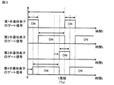
- FIG. FIG. 6 is a duty ratio locus diagram for the duty ratio D501 and the duty ratio D502 when the voltage of the AC power supply 1 is positive.
- FIG. 7 is a duty ratio locus diagram of the duty ratio D501 and the duty ratio D502 when the voltage of the AC power supply 1 is negative.
- FIG. 17 is a diagram illustrating an example of gate pulses of the first semiconductor device 501, the second semiconductor device 502, the third semiconductor device 601, and the fourth semiconductor device 602 in the first control method.
- FIG. 16 is a diagram illustrating another example of gate pulses of the first semiconductor device 501, the second semiconductor device 502, the third semiconductor device 601, and the fourth semiconductor device 602 in the first control method. It is a figure showing the locus of duty ratio D501 and duty ratio D502 which satisfy
- FIG. 16 is a diagram illustrating another example of gate pulses of the first semiconductor device 501, the second semiconductor device 502, the third semiconductor device 601, and the fourth semiconductor device 602 in the second control method.
- FIG. 2 represents a plurality of control blocks responsible for a first control scheme. It is a figure showing several control blocks in charge of a 3rd control system.
- FIG. 1 It is a figure showing several control blocks in charge of a 2nd control system. It is a figure showing the control block 151 which produces
- FIG. It is a figure showing the control block 152 which produces
- control block 153 which generates command value D501c of duty ratio D501, and command value D502c of duty ratio D502.
- the control block 154 which produces
- FIG. 7 is a diagram illustrating a control block 156 that generates a low duty ratio Dlimit. It is a figure showing control block 157 which generates command value iout_ref of output current. It is a figure showing control block 158 which generates command value Dpsc of phase shift amount Dps. It is a figure showing the control block 159 which produces
- control block 165 which generates gate signals g11 and g12 for semiconductor elements which constitute the first leg 500. It is a figure showing control block 166 which generates gate signals g21 and g22 for semiconductor elements which constitute the 2nd leg 600. It is a figure showing the control block 167 which produces
- control block 168 which produces
- FIG. 10 is a diagram illustrating a control method in a first modification of the first embodiment.
- FIG. 16 is a diagram illustrating a control method in a second modification of the first embodiment.
- FIG. 16 is a diagram illustrating a control method in a third modification of the first embodiment.
- FIG. 10 is a diagram illustrating a control method in Embodiment 2.
- FIG. 1 The figure showing the example of the gate pulse of the 1st semiconductor element 501 in the 4th control method, the 2nd semiconductor element 502, the 3rd semiconductor element 601, the 4th semiconductor element 602, the 5th semiconductor element 301, and the 6th semiconductor element 302. It is. Another example of the gate pulse of the first semiconductor device 501, the second semiconductor device 502, the third semiconductor device 601, the fourth semiconductor device 602, the fifth semiconductor device 301, and the sixth semiconductor device 302 in the fourth control method will be described. FIG. Another example of the gate pulse of the first semiconductor device 501, the second semiconductor device 502, the third semiconductor device 601, the fourth semiconductor device 602, the fifth semiconductor device 301, and the sixth semiconductor device 302 in the sixth control method will be described. FIG.
- FIG. The figure showing the example of the gate pulse of the 1st semiconductor element 501 in the 5th control method, the 2nd semiconductor element 502, the 3rd semiconductor element 601, the 4th semiconductor element 602, the 5th semiconductor element 301, and the 6th semiconductor element 302. It is.
- FIG. Another example of the gate pulse of the first semiconductor device 501, the second semiconductor device 502, the third semiconductor device 601, the fourth semiconductor device 602, the fifth semiconductor device 301, and the sixth semiconductor device 302 in the fifth control method will be described.
- FIG. 16 is a diagram illustrating a control method in a first modification of the second embodiment.
- FIG. 17 is a diagram illustrating a control method in a second modification of the second embodiment.
- FIG. 17 is a diagram illustrating a control method in a third modification of the second embodiment.
- FIG. 10 is a diagram illustrating another modification of the secondary side rectification circuit 11.
- FIG. 10 is a diagram illustrating another modification of the secondary side rectification circuit 11.
- FIG. 10 is a diagram illustrating another modification of the secondary side rectification circuit 11.
- FIG. 10 is a diagram illustrating another modification of the secondary side rectification circuit 11.
- FIG. 10 is a diagram illustrating another modification of the secondary side rectification circuit 11.
- FIG. 16 is a diagram illustrating a modification of output smoothing circuit 1200.
- FIG. 16 shows another modification of output smoothing circuit 1200. It is a figure showing the modification of control circuit 14.
- FIG. 10 is a diagram illustrating another modification of the secondary side rectification circuit 11.
- FIG. 10 is a diagram illustrating another modification of the secondary side rectification circuit 11.
- FIG. 16 is a diagram illustrating a modification of output smoothing circuit 1200.
- FIG. 16 shows another modification of output smoothing circuit 1200. It is a figure showing the modification of control circuit 14.
- Embodiments will be described below with reference to the drawings.
- Embodiment 1 The power conversion device of the first embodiment is applied to a power supply system centering on a charger of an electric vehicle.
- FIG. 1 is a diagram showing a configuration of power conversion device 5000 according to the first embodiment.
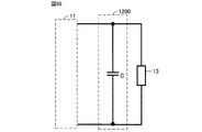
- the power conversion device 5000 converts AC power supplied from the AC power supply 1 into DC power, and outputs DC power to the DC load 13.
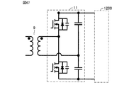
- Power converter 5000 includes a power factor improving reactor 2, a DC capacitor 4, a third leg 300, an inverter circuit 655, a series resonance reactor 7, a parallel resonance reactor 8, a transformer 9, and a series resonance.
- a capacitor 10, a secondary side rectifier circuit 11, and an output smoothing circuit 1200 are provided.
- the inverter circuit 655 includes a first leg 500 and a second leg 600.
- the AC power supply 1 is a commercial AC system or a private generator.
- the direct current load 13 is, for example, a high voltage battery for traveling a vehicle or a lead battery which is a power supply of vehicle electrical components.
- the DC load 13 may be a DC load requiring other AC input and insulation, and may be configured by, for example, an electric double layer capacitor (EDLC).
- EDLC electric double layer capacitor
- the first leg 500, the second leg 600, the third leg 300, and the DC capacitor 4 are connected in parallel.
- the first leg 500 includes a first semiconductor device 501 and a second semiconductor device 502 connected in series.
- the second leg 600 includes a third semiconductor device 601 and a fourth semiconductor device 602 connected in series.
- the third leg 300 includes a fifth semiconductor device 301 and a sixth semiconductor device 302 connected in series.
- the first semiconductor device 501, the third semiconductor device 601, and the fifth semiconductor device 301 are connected.
- the second semiconductor element 502, the fourth semiconductor element 602, and the sixth semiconductor element 302 are connected.
- the first semiconductor device 501 is located diagonally to the fourth semiconductor device 602.
- the second semiconductor element 502 is located diagonally to the third semiconductor element 601.
- a rectangular wave voltage is applied to the primary side terminal of the transformer 9 by turning on the two semiconductor elements in the diagonally located relationship included in the first leg 500 and the second leg 600 to the DC load 13. Transmit power.
- diodes are connected in anti-parallel to each of the first semiconductor element 501, the second semiconductor element 502, the third semiconductor element 601, and the fourth semiconductor element 602, and a capacitor is provided. Connected in parallel.
- the diode connected antiparallel to the semiconductor element may be an external diode or a body diode of the semiconductor element.
- an external capacitor may be used, or a parasitic capacitor of the semiconductor element may be used.
- a first AC end ND1 which is a connection point of the first semiconductor element 501 and the second semiconductor element 502 is connected to one end of the AC power supply 1 via the power factor improving reactor 2.
- the third semiconductor element 601 and the fourth semiconductor element 602 are connected at the second AC terminal ND2.
- a third AC end ND3 which is a connection point of the fifth semiconductor element 301 and the sixth semiconductor element 302 is connected to the other end of the AC power supply 1.
- Power factor improving reactor 2 is a current reducing reactor having one end connected to AC power supply 1 and the other end connected to inverter circuit 655.
- the power factor improving reactor 2 may be connected to the other terminal side of the AC power supply 1 or may be dispersedly connected to both ends of the AC power supply 1.
- the side connected to the AC power supply 1 with respect to the transformer 9 is referred to as a primary side, and the side connected to the DC load 13 with respect to the transformer 9 is referred to as a secondary side.
- One end of the primary side winding of the transformer 9 is connected to the first AC end ND1 via the series resonance reactor 7.
- the other end of the primary side winding of the transformer 9 is connected to the second AC end ND2 via the series resonance capacitor 10.
- the secondary winding of transformer 9 is magnetically coupled to the primary winding.
- the parallel resonance reactor 8 is connected in parallel to the primary side winding of the transformer 9.
- a resonance circuit is configured by the series resonance reactor 7, the parallel resonance reactor 8, and the series resonance capacitor 10.
- the secondary side rectification circuit 11 rectifies the AC output from the secondary side winding of the transformer 9.
- the secondary side rectifier circuit 11 includes a plurality of diodes.
- the output smoothing circuit 1200 is disposed between the secondary side rectifier circuit 11 and the DC load 13.
- the output smoothing circuit 1200 includes a first output smoothing capacitor 1201 and a second output smoothing capacitor 1203 connected in parallel.
- the output smoothing circuit 1200 includes an output smoothing reactor 1202 disposed between the first output smoothing capacitor 1201 and the second output smoothing capacitor 1203.
- the power conversion device 5000 includes a first voltage detector 675, a second voltage detector 676, a third voltage detector 677, a first current detector 678, and a second current detector 679.
- the first voltage detector 675 detects the DC voltage Vdc of the DC capacitor 4.
- the second voltage detector 676 detects the voltage across the second output smoothing capacitor 1203 to detect the output voltage Vout.
- the third voltage detector 677 detects the voltage vac of the AC power supply 1.
- the first current detector 678 detects the current iac of the AC power supply 1.
- the second current detector 679 detects the output current iout.
- the detected values of the respective voltages and currents are supplied to the control circuit 14, and the control circuit 14 performs an operation.
- the control circuit 14 outputs these calculation results to the gate terminals of the semiconductor elements 301 to 302, 501 to 502, and 601 to 602, respectively.
- the on / off state of the fifth semiconductor element 301 and the sixth semiconductor element 302 is switched according to the polarity of the voltage input from the AC power supply 1. Specifically, while the voltage vac of the AC power supply 1 is positive, the sixth semiconductor element 302 is turned on, and the fifth semiconductor element 301 is turned off. On the other hand, while the voltage vac of the AC power supply 1 is negative, the fifth semiconductor element 301 is turned on and the sixth semiconductor element 302 is turned off.
- the fifth semiconductor element 301 and the sixth semiconductor element 302 are active semiconductors.
- the active semiconductor is reduced in conduction loss by performing synchronous rectification.
- the fifth semiconductor element 301 and the sixth semiconductor element 302 are not limited to IGBTs (Insulated Gate Bipolar Transistors) or MOSFETs (Metal Oxide Semiconductor Field Effect Transistors), but also to SiC (Silicon Carbide) -MOSFETs, GaN (Gallium Nitride)
- An active semiconductor such as a -FET or a GaN-HEMT (High Electron Mobility Transistor) may be used.
- n is a ratio of the primary winding number N1 to the secondary winding number N2 of the transformer 9, and is expressed by the equation (7).
- fr is a resonant frequency calculated from the inductance (Lr) of the series resonant reactor 7 and the capacitance (Cr) of the series resonant capacitor 10, and is expressed by the equation (8).
- k is a ratio of the inductance (Lm) of the parallel resonance reactor 8 to the inductance (Lr) of the series resonance reactor 7, and is expressed by the equation (9).
- Q in equation (6) is the resonance sharpness and is expressed by equation (10).
- fs is a switching frequency of the semiconductor elements 501 to 502 and 601 to 602.
- FIG. 2 is a graph showing the characteristics of the voltage conversion ratio of equation (6).
- the horizontal axis in FIG. 2 represents the ratio of the switching frequency fs to the resonant frequency fr, that is, the normalized frequency.
- the vertical axis represents the voltage conversion ratio.
- FIG. 2 in the region where the normalized frequency is less than 1, it is possible to obtain a voltage conversion ratio higher than the turns ratio n.
- a switching frequency having a larger value is selected among two switching frequencies. Note that a switching frequency having a smaller value may be selected among the two switching frequencies.
- the sensitivity of the voltage conversion ratio to the normalized frequency is high.
- the region where the normalized frequency is 1 or more a voltage conversion ratio equal to or less than the reciprocal (1 / n) of the turns ratio n is obtained, and the sensitivity of the voltage conversion ratio to the normalized frequency is degraded. Therefore, when the output voltage Vout is to be step-down controlled over a wide range only by the frequency modulation control, the frequency fluctuation range must be significantly increased. As a result, when the power loss of the semiconductor element and the magnetic component increases, the power conversion efficiency is lowered, and the semiconductor element and the magnetic component may be broken.
- power conversion device 5000 of the present embodiment performs pulse frequency modulation in addition to pulse width modulation control based on comparison between the target value of the voltage conversion ratio arbitrarily set for second leg 600 and the threshold value.
- High power factor control and output control are simultaneously performed by selecting and executing at least one of control and phase shift control. As a result, a wide range of voltage control is possible without significantly increasing the frequency fluctuation range.
- FIG. 3 is a diagram for explaining two threshold values of the power conversion ratio.
- the threshold TH1 and the threshold TH2 can be set as follows.
- FIG. 4 is a diagram showing a control method in the first embodiment.
- high power factor control is performed by the first semiconductor element 501 and the second semiconductor element 502 constituting the first leg 500, and the third semiconductor element 601 and the fourth semiconductor element constituting the second leg 600.
- the output control is performed to perform the rectifying operation in accordance with the polarity of the voltage of the AC power supply 1 between the fifth semiconductor element 301 and the sixth semiconductor element 302 that constitute the third leg 300.
- the control circuit 14 controls the first leg 500, the second leg 600, and the third leg 300 based on the first control method in a region where the target value M * of the voltage conversion ratio M is larger than the threshold TH1.
- the control circuit 14 controls the first leg 500 by pulse width modulation control and pulse frequency modulation control.
- the control circuit 14 controls the second leg 600 by pulse width modulation control and pulse frequency modulation control.
- the control circuit 14 controls the third leg 300 to perform rectification.
- the control circuit 14 controls the first leg 500, the second leg 600, and the third leg 300 based on the second control method in a region where the target value M * of the voltage conversion ratio M is less than or equal to the threshold TH1 and greater than the threshold TH2. Control.
- the control circuit 14 controls the first leg 500 by pulse width modulation control and pulse frequency modulation control.
- the control circuit 14 controls the second leg 600 by pulse width modulation control, pulse frequency modulation control, and phase shift modulation control.
- the control circuit 14 controls the third leg 300 to perform rectification.
- the control circuit 14 controls the first leg 500, the second leg 600, and the third leg 300 based on the third control method in a region where the target value M * of the voltage conversion ratio M is less than or equal to the threshold TH2.
- the control circuit 14 controls the first leg 500 by pulse width modulation control.
- the control circuit 14 controls the second leg 600 by pulse width modulation control and phase shift modulation control.
- the control circuit 14 controls the third leg 300 to perform rectification.
- the first embodiment it is possible to suppress the generation loss by using the second control method.
- pulse width modulation control is essential. Furthermore, when it is necessary to lower the output voltage with respect to the input voltage, it is necessary to increase the frequency as much as possible not only by the frequency modulation control, but this becomes a factor of excess loss.
- phase shift control when the phase shift amount increases without limit, reactive power becomes excessive and causes loss. From these things, appropriate control becomes possible by combining three types of modulation control.
- voltage control can be performed in a narrow frequency band.
- the phase shift is used in a region where the power conversion ratio is small, in consideration of the fact that the output voltage is lowered relative to the input voltage.
- the control circuit 14 causes the third leg 300 to perform the rectifying operation by inverting the timing at which the fifth semiconductor element 301 is turned on and the timing at which the sixth semiconductor element 302 is turned on.
- the control circuit 14 switches the fifth semiconductor element 301 and the sixth semiconductor element 302 between the on state and the off state according to the polarity of the voltage input from the AC power supply 1. Specifically, the control circuit 14 turns on the sixth semiconductor element 302 and turns off the fifth semiconductor element 301 while the voltage vac of the AC power supply 1 is positive. On the other hand, the control circuit 14 turns on the fifth semiconductor element 301 and turns off the sixth semiconductor element 302 while the voltage vac of the AC power supply 1 is negative.
- the control circuit 14 controls the current iac of the AC power supply 1 to have a high power factor by controlling the first semiconductor element 501 and the second semiconductor element 502 that constitute the first leg 500 using pulse width modulation control. Do.
- power converter 5000 Since power converter 5000 has a bridgeless rectifier configuration, the duty ratio must be switched according to the polarity of voltage vac of AC power supply 1.
- the duty ratio D501 and the duty ratio D502 of the first leg 500 are defined as in the following equations.
- Vdc in Formula (13) and Formula (14) is a voltage of the direct current capacitor 4.
- FIG. 5 is a duty ratio locus diagram for the duty ratio D501 and the duty ratio D502 when the voltage of the AC power supply 1 is positive. In the zero phase and the half cycle ( ⁇ ) phase, since the voltage of the AC power supply 1 is zero, the duty ratio D501 is as close to zero as possible, and the duty ratio D502 is as close to one as possible.
- control circuit 14 switches the first semiconductor element 501 with the duty ratio D501 of equation (13), and the second semiconductor element 502 with the duty ratio D502 of equation (14). Control.
- FIG. 6 is a duty ratio locus diagram of the duty ratio D501 and the duty ratio D502 when the voltage of the AC power supply 1 is negative.
- the duty ratio D501 is as close to 1 as possible
- the duty ratio D502 is as close to zero as possible.
- the control circuit 14 switches the first semiconductor element 501 at the duty ratio of equation (14) and switches the second semiconductor element 502 at the duty ratio of equation (13). .
- a smaller duty ratio is defined as a low duty ratio Dlimit, as shown in the equation (15), FIG. 5 and FIG.
- the duty ratio is set according to the voltage polarity of the AC power supply 1 regardless of the magnitude relation between the threshold of the voltage conversion ratio arbitrarily set and the target value of the voltage conversion ratio.
- high power factor control is achieved using pulse width modulation control.
- Each semiconductor element is not limited to IGBT (Insulated Gate Bipolar Transistor) or MOSFET (Metal Oxide Semiconductor Field Effect Transistor), but also to SiC (Silicon Carbide) -MOSFET, GaN (Gallium Nitride) -FET, GaN- A HEMT (High Electron Mobility Transistor) may be used.
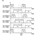
- FIG. 7 is a diagram showing an example of gate pulses of the first semiconductor device 501, the second semiconductor device 502, the third semiconductor device 601, and the fourth semiconductor device 602 in the first control method.
- the first semiconductor element 501 and the second semiconductor element 502 are subjected to high power factor control using pulse width modulation control and pulse frequency modulation control.
- the third semiconductor element 601 and the fourth semiconductor element 602 are output controlled using pulse width modulation control and pulse frequency modulation control.
- the timing at which the first semiconductor element 501 is turned on and the timing at which the fourth semiconductor element 602 is turned on is synchronized, the timing at which the second semiconductor element 502 is turned off, and the third semiconductor element 601 is turned off. Synchronize with the timing of Furthermore, the pulse width of the first semiconductor element 501 and the pulse width of the third semiconductor element 601 are equal, and the pulse width of the second semiconductor element 502 and the pulse width of the fourth semiconductor element 602 are equal.
- the control circuit 14 sets the switching frequency fs common to the first semiconductor element 501, the second semiconductor element 502, the third semiconductor element 601, and the fourth semiconductor element 602 while changing such conditions while satisfying such conditions.
- the first semiconductor element 501, the second semiconductor element 502, the third semiconductor element 601, and the fourth semiconductor element 602 are controlled.
- FIG. 8 is a diagram illustrating another example of gate pulses of the first semiconductor device 501, the second semiconductor device 502, the third semiconductor device 601, and the fourth semiconductor device 602 in the first control method.
- the central phase of the gate pulse of the first semiconductor element 501 and the central phase of the gate pulse of the fourth semiconductor element 602 are synchronized, and the central phase of the gate pulse of the second semiconductor element 502 and the third phase
- the center phase of the gate pulse of the semiconductor element 601 is synchronized.
- the pulse width of the first semiconductor element 501 and the pulse width of the third semiconductor element 601 are equal, and the pulse width of the second semiconductor element 502 and the pulse width of the fourth semiconductor element 602 are equal.
- the control circuit 14 sets the switching frequency fs common to the first semiconductor element 501, the second semiconductor element 502, the third semiconductor element 601, and the fourth semiconductor element 602 while changing such conditions while satisfying such conditions.
- the first semiconductor element 501, the second semiconductor element 502, the third semiconductor element 601, and the fourth semiconductor element 602 are controlled.
- the length of the period in which the first semiconductor element 501 and the fourth semiconductor element 602 located at the diagonal are simultaneously turned on and the second semiconductor element 502 and the third located at the diagonal Since the length of the period during which the semiconductor element 601 is simultaneously turned on can be made the same, stable power supply becomes possible.
- phase shift control In phase shift control, the phase of the second leg 600 is shifted by the phase shift amount Dps with respect to the phase of the first leg 500.
- the phase shift amount is represented as the duty ratio.
- the phase shift amount Dps needs to be always lower than the duty ratio D501 and the duty ratio D502. That is, as shown in equation (15), the phase shift amount Dps must always be smaller than the smaller duty ratio Dlimit among the duty ratio D501 and the duty ratio D502. This relationship can be expressed by equation (16).
- FIG. 9 is a diagram showing the locus of the duty ratio D501 and the duty ratio D502 satisfying the relationship of equation (16) and the phase shift amount Dps.
- the horizontal axis is the phase of the voltage vac of the AC power supply 1. In the vicinity of the zero phase, since the low duty ratio Dlimit is as close to zero as possible in principle, the relationship of the equation (16) can not be satisfied.
- control phase shift amount Dps_limit represented by the equation (17) is used for control.
- phase shift amount Dps obtained by the control circuit 14 is smaller than Dlimit, control is performed using the phase shift amount Dps. If the phase shift amount Dps obtained by the control circuit 14 exceeds Dlimit, control is performed using Dlimit.
- control phase shift amount Dps_limit can always be set to the variable duty ratio Dlimit or less.
- FIG. 10 is a diagram showing an example of gate pulses of the first semiconductor device 501, the second semiconductor device 502, the third semiconductor device 601, and the fourth semiconductor device 602 in the third control method.
- the initial state of the phase shift control is synchronized with the timing when the first semiconductor element 501 turns on and the timing when the fourth semiconductor element 602 turns on, and the timing when the second semiconductor element 502 turns off 3) It is defined as a state synchronized with the timing at which the semiconductor element 601 is turned off. From this initial state, the phase of the third semiconductor element 601 and the phase of the fourth semiconductor element 602 shift. Furthermore, the pulse width of the first semiconductor element 501 and the pulse width of the third semiconductor element 601 are equal, and the pulse width of the second semiconductor element 502 and the pulse width of the fourth semiconductor element 602 are equal.
- the control circuit 14 controls the first semiconductor element 501, the second semiconductor element 502, the third semiconductor element 601, and the fourth semiconductor element 602 so as to satisfy such conditions.
- FIG. 11 is a diagram illustrating another example of gate pulses of the first semiconductor device 501, the second semiconductor device 502, the third semiconductor device 601, and the fourth semiconductor device 602 in the third control method.
- the initial state of the phase shift control is synchronized with the timing at which the second semiconductor element 502 is turned on, with the timing when the first semiconductor element 501 is turned on and the timing when the third semiconductor element 601 is turned on.
- It is defined as a state synchronized with the timing at which the semiconductor element 602 is turned on. From this initial state, the phase of the third semiconductor element 601 and the phase of the fourth semiconductor element 602 shift. Furthermore, the pulse width of the first semiconductor element 501 and the pulse width of the third semiconductor element 601 are equal, and the pulse width of the second semiconductor element 502 and the pulse width of the fourth semiconductor element 602 are equal.
- the control circuit 14 controls the first semiconductor element 501, the second semiconductor element 502, the third semiconductor element 601, and the fourth semiconductor element 602 so as to satisfy such conditions.
- FIG. 12 is a diagram illustrating an example of gate pulses of the first semiconductor device 501, the second semiconductor device 502, the third semiconductor device 601, and the fourth semiconductor device 602 in the second control method.
- the initial state of phase shift control is synchronized with the timing when the first semiconductor element 501 turns on and the timing when the fourth semiconductor element 602 turns on, and the timing when the second semiconductor element 502 turns off 3) It is defined as a state synchronized with the timing at which the semiconductor element 601 is turned off. From this initial state, the phase of the third semiconductor element 601 and the phase of the fourth semiconductor element 602 shift. Furthermore, the pulse width of the first semiconductor element 501 and the pulse width of the third semiconductor element 601 are equal, and the pulse width of the second semiconductor element 502 and the pulse width of the fourth semiconductor element 602 are equal.
- the control circuit 14 sets the switching frequency fs common to the first semiconductor element 501, the second semiconductor element 502, the third semiconductor element 601, and the fourth semiconductor element 602 while changing such conditions while satisfying such conditions.
- the first semiconductor element 501, the second semiconductor element 502, the third semiconductor element 601, and the fourth semiconductor element 602 are controlled.
- FIG. 13 is a diagram illustrating another example of gate pulses of the first semiconductor device 501, the second semiconductor device 502, the third semiconductor device 601, and the fourth semiconductor device 602 in the second control method.
- the initial state of phase shift control is synchronized with the timing at which the second semiconductor element 502 is turned on and the timing at which the first semiconductor element 501 is turned on and the timing at which the third semiconductor element 601 is turned on.
- It is defined as a state synchronized with the timing at which the semiconductor element 602 is turned on. From this initial state, the phase of the third semiconductor element 601 and the phase of the fourth semiconductor element 602 shift. Furthermore, the pulse width of the first semiconductor element 501 and the pulse width of the third semiconductor element 601 are equal, and the pulse width of the second semiconductor element 502 and the pulse width of the fourth semiconductor element 602 are equal.
- the control circuit 14 sets the switching frequency fs common to the first semiconductor element 501, the second semiconductor element 502, the third semiconductor element 601, and the fourth semiconductor element 602 while changing such conditions while satisfying such conditions.
- the first semiconductor element 501, the second semiconductor element 502, the third semiconductor element 601, and the fourth semiconductor element 602 are controlled.
- the control circuit 14 adds the third semiconductor element 601 and the fourth semiconductor element 602 to pulse width modulation control, and generates a gate signal based on at least one of frequency modulation control and phase shift control, Perform output control.
- Each semiconductor element is not limited to IGBT (Insulated Gate Bipolar Transistor) or MOSFET (Metal Oxide Semiconductor Field Effect Transistor), but also to SiC (Silicon Carbide) -MOSFET, GaN (Gallium Nitride) -FET, GaN- A HEMT (High Electron Mobility Transistor) may be used.
- the control circuit 14 comprises a plurality of control blocks.
- Power converter 5000 has a constant power (Constant Power: CP) control mode in which input power pac (Iac ⁇ Vac ⁇ power factor) is constant, and a constant current (CC: Constant Current: CC) in which output current iout is constant. And a control mode.
- Constant Power: CP Constant Power: CP
- CC Constant Current: CC
- FIG. 14 is a diagram representing a plurality of control blocks responsible for the first control method.
- the control block 151 turns the gate signal g5 of the fifth semiconductor element 301 to low level to turn off the fifth semiconductor element 301, and the gate signal g6 of the sixth semiconductor element 302.
- the sixth semiconductor element 302 is turned on.
- the control block 151 turns the gate signal g5 of the fifth semiconductor element 301 to high level to turn on the fifth semiconductor element 301, and the gate signal g6 of the sixth semiconductor element 302. To a low level to turn off the sixth semiconductor element 302.
- control block 152 In the CP control mode, the control block 152 outputs the current command value iac_ref_cp of the AC power supply 1 for CP control mode given from the outside as the current command value iac_ref of the AC power supply 1.
- control block 152 AC power supply for CC control mode obtained by proportional-plus-integral control of a feedback amount obtained by subtracting DC voltage Vdc of DC capacitor 4 from voltage command value Vdc_ref of DC capacitor 4
- the current command value iac_ref_cp of 1 is output as the current command value iac_ref of the AC power supply 1.
- Control block 153 includes voltage vac of AC power supply 1, effective voltage Vac of AC power supply 1, current iac of AC power supply 1, current command value iac_ref of AC power supply 1, DC voltage Vdc of DC capacitor 4, DC voltage of DC capacitor 4 Based on the command value Vdc_ref, a command value D501c of the duty ratio D501 and a command value D502c of the duty ratio D502 are generated.
- the control block 154 When the voltage vac of the AC power supply 1 is positive, the control block 154 outputs the command value D501c of the duty ratio D501 as the command value D1c of the duty ratio of the first semiconductor element 501.
- the control block 154 outputs the command value D 502 c of the duty ratio D 502 as the command value D 1 c of the duty ratio of the first semiconductor element 501 when the voltage vac of the AC power supply 1 is negative.
- the control block 155 outputs the command value D502c of the duty ratio D502 as the command value D2c of the duty ratio of the second semiconductor element 502 when the voltage vac of the AC power supply 1 is positive.
- the control block 155 outputs the command value D501c of the duty ratio D501 as the command value D2c of the duty ratio of the second semiconductor element 502.
- control block 157 In the CC control mode, the control block 157 outputs a current command value iout_ref_cc of an output current for CC control mode given from the outside as a current command value iout_ref of the output current.
- Control block 157 is an output for CP control mode obtained by performing proportional integral control on a feedback amount obtained by subtracting DC voltage Vdc of DC capacitor 4 from voltage command value Vdc_ref of DC capacitor 4 in the CP control mode.
- the current command value iout_ref_cc of the current is output as the current command value iout_ref of the output current.
- the control block 169 subtracts the output current iout from the command value iout_ref of the output current output from the control block 157 to calculate the difference current, and outputs the command value fs_ref of the switching frequency by performing proportional control of the difference current. .
- the control block 165 When the command value D 502 c of the duty ratio D 502 output from the control block 153 is smaller than the carrier wave having the frequency component of the command value fs_ref of the switching frequency output from the control block 169, the control block 165 The first gate signal g11 is set to the high level, and the second gate signal g12 for the first leg is set to the low level. If the command value D 502 c of the duty ratio D 502 output from the control block 153 is greater than or equal to the carrier wave having the frequency component of the switching frequency command value fs_ref output from the control block 169, the control block 165 The first gate signal g11 is set to the low level, and the second gate signal g12 for the first leg is set to the high level.
- the control block 175 for the second leg And the second gate signal g22 for the second leg is set to the low level. If the command value D501c of the duty ratio D501 output from the control block 153 is equal to or higher than the carrier wave having the frequency component of the command value fs_ref of the switching frequency output from the control block 169, the control block 175 The first gate signal g21 is set to the low level, and the second gate signal g22 for the second leg is set to the high level.
- the control block 167 outputs the first gate signal g11 for the first leg as the gate signal g1 of the first semiconductor element 501 when the voltage vac of the AC power supply 1 is positive, and the second gate for the first leg The signal g12 is output as the gate signal g2 of the second semiconductor element 502.
- the control block 167 outputs the second gate signal g12 for the first leg as the gate signal g1 of the first semiconductor element 501 when the voltage vac of the AC power supply 1 is negative, and the first gate signal for the first leg g11 is output as the gate signal g2 of the second semiconductor element 502.
- the control block 168 outputs the first gate signal g21 for the second leg as the gate signal g3 of the third semiconductor element 601 when the voltage vac of the AC power supply 1 is positive, and the second gate for the second leg The signal g22 is output as the gate signal g4 of the fourth semiconductor element 602.
- the control block 168 outputs the second gate signal g22 for the second leg as the gate signal g3 of the third semiconductor element 601 when the voltage vac of the AC power supply 1 is negative, and the first gate signal for the second leg g21 is output as the gate signal g4 of the fourth semiconductor element 602.
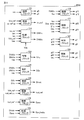
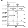
- FIG. 15 is a diagram representing a plurality of control blocks responsible for the third control method.
- the plurality of control blocks of the third control method is different from the plurality of control blocks of the first control method in that the control block of the third control method is a control block instead of the control block 169. 156, 158 and 159, and instead of the control blocks 165 and 175, control blocks 176 and 177 are included.
- the control block 156 lowers the command value D1c of the duty ratio of the first semiconductor element 501.
- the duty ratio is output as Dlimit.
- the control block 156 lowers the command value D2c of the duty ratio of the second semiconductor element 502. Output as the ratio Dlimit.
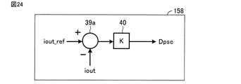
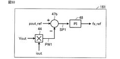
- the control block 158 outputs a command value Dpsc of a phase shift amount Dps obtained by proportionally controlling a difference current as a feedback amount obtained by subtracting the output current iout from the command value iout_ref of the output current.
- the control block 159 When the low duty ratio Dlimit is equal to or greater than the command value Dpsc, the control block 159 outputs the command value Dpsc as the command value Dps_limitc of the control phase shift amount Dps_limit. When the low duty ratio Dlimit is smaller than the command value Dpsc, the control block 159 outputs the low duty ratio Dlimit as the command value Dps_limitc of the control phase shift amount Dps_limit.
- the control block 176 sets the first gate signal g11 for the first leg to the high level, and for the first leg.
- the second gate signal g12 is set to low level.
- the control block 176 sets the first gate signal g11 for the first leg to the low level when the command value D502c of the duty ratio D502 is equal to or greater than the carrier wave having the fixed switching frequency fs0 frequency component, and sets the first leg signal for the first leg. 2. Make the gate signal g12 high.
- the control block 177 sets the command value D2c of the duty ratio of the second semiconductor element 502 (when the voltage vac of the AC power supply 1 is positive) or the command value D1c of the duty ratio of the first semiconductor element 501 (voltage vac of the AC power supply 1). Is negative polarity) and the command value Dps_limitc of the control phase shift amount Dps_limit output from the control block 159, and the sum W is obtained.
- the control block 177 If the carrier wave having the frequency component at the fixed switching frequency fs0 is equal to or higher than the command value Dps_limitc, and the sum W is at least the carrier wave having the frequency component at the fixed switching frequency fs0, the control block 177
- the second gate signal g22 for the leg is set to the high level
- the first gate signal g11 for the first leg is set to the low level.
- the control block 177 When the carrier wave having the frequency component at the fixed switching frequency fs0 is equal to or higher than the command value Dps_limitc and the sum W is smaller than the carrier wave having the frequency component at the fixed switching frequency fs0, the control block 177 The second gate signal g22 for two legs is set to the low level, and the first gate signal g11 for the first leg is set to the high level. The control block 177 performs the second operation when the carrier wave having the frequency component at the fixed switching frequency fs0 is smaller than the command value Dps_limitc and the sum W is higher than the carrier wave having the frequency component at the fixed switching frequency fs0.
- the second gate signal g22 for the leg is set to the low level, and the first gate signal g11 for the first leg is set to the high level.
- the control block 177 determines that the carrier wave having the frequency component at the fixed switching frequency fs0 is smaller than the command value Dps_limitc, and the sum W is smaller than the carrier wave having the frequency component at the fixed switching frequency fs0.
- the second gate signal g22 for two legs is set to the low level, and the first gate signal g11 for the first leg is set to the high level.
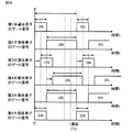
- FIG. 16 is a diagram showing a plurality of control blocks in charge of the second control method.
- the difference between the plurality of control blocks of the second control method and the plurality of control blocks of the first control method is that the control block of the second control method is a control block instead of the control block 169. 156, 158, 159, 160, and instead of the control block 175, a control block 166 is included.
- control blocks 156, 158, 159 are the same as those described in the third control scheme and will not be repeated.
- the control block 160 multiplies the output voltage PW obtained by multiplying the output voltage Vout by the output current iout, the input voltage obtained by multiplying the effective voltage Vac of the alternating current power supply 1 and the effective current Iac of the alternating current power supply 1
- the conversion efficiency ⁇ is determined by dividing by PW2.
- the control block 160 proportionally integrates the difference efficiency S ⁇ as a feedback amount obtained by subtracting a predetermined target efficiency ⁇ ref and the conversion efficiency ⁇ , and outputs a command value fs_ref of the switching frequency.
- the control block 166 sets the command value D2c of the duty ratio of the second semiconductor element 502 (when the voltage vac of the AC power supply 1 is positive) or the command value D1c of the duty ratio of the first semiconductor element 501 (voltage vac of the AC power supply 1). Is negative polarity) and the command value Dps_limitc of the control phase shift amount Dps_limit output from the control block 159, and the sum W is obtained.
- control block 166 the carrier wave having the frequency component of command value fs_ref of the switching frequency output from control block 160 is greater than or equal to command value Dps_limitc, and the sum W is a command of the switching frequency output from control block 160 If it is higher than the carrier wave having the frequency component of the value fs_ref, the second gate signal g22 for the second leg is set to the high level, and the first gate signal g11 for the first leg is set to the low level.
- control block 166 the carrier wave having the frequency component of command value fs_ref of the switching frequency output from control block 160 is greater than or equal to command value Dps_limitc, and the sum W is a command of the switching frequency output from control block 160 If it is smaller than the carrier wave having a frequency component of value fs_ref, the second gate signal g22 for the second leg is set to the low level, and the first gate signal g11 for the first leg is set to the high level.
- control block 166 the carrier wave having a frequency component of command value fs_ref of the switching frequency output from control block 160 is smaller than command value Dps_limitc, and the sum W is a command of the switching frequency output from control block 160 If it is equal to or higher than the carrier wave having a frequency component of value fs_ref, the second gate signal g22 for the second leg is set to the low level, and the first gate signal g11 for the first leg is set to the high level.
- control block 166 the carrier wave having a frequency component of command value fs_ref of the switching frequency output from control block 160 is smaller than command value Dps_limitc, and the sum W is a command of the switching frequency output from control block 160 If it is smaller than the carrier wave having a frequency component of value fs_ref, the second gate signal g22 for the second leg is set to the low level, and the first gate signal g11 for the first leg is set to the high level.
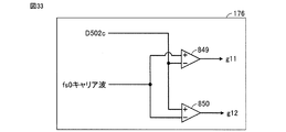
- FIG. 17 is a diagram showing a control block 151 that generates a gate signal g5 of the fifth semiconductor device 301 and a gate signal g6 of the sixth semiconductor device 302 of the third leg 300.
- the control block 151 includes a comparator 15 and a logical NOT circuit 979.
- the comparator 15 compares the voltage vac of the AC power supply 1 detected by the third voltage detector 677 with the ground voltage.
- a logical NOT circuit 979 receives the output of the comparator 15.
- the comparator 15 outputs the gate signal g6 of the sixth semiconductor element 302.
- the gate signal g5 of the fifth semiconductor element 301 is output from the logical NOT circuit 979.
- control block 151 The operation of the control block 151 will be described.
- the output of the comparator 15 is at the high level.
- the gate signal g6 of the sixth semiconductor element 302 becomes high level, and the sixth semiconductor element 302 is turned on.
- the gate signal g5 of the fifth semiconductor element 301 becomes low level, and the fifth semiconductor element 301 is turned off.
- the output 15 of the comparator is at the low level.
- the gate signal of the sixth semiconductor element 302 becomes low level, and the sixth semiconductor element 302 is turned off.
- the gate signal of the fifth semiconductor element 301 becomes high level, and the fifth semiconductor element 301 is turned on.
- FIG. 18 is a diagram showing control block 152 for generating current command value iac_ref of AC power supply 1.
- the control block 152 includes a subtractor 68, a PI control unit 69, and a selector 18.
- the subtractor 68 subtracts the DC voltage Vdc of the DC capacitor 4 detected by the first voltage detector 675 from the voltage command value Vdc_ref of the DC capacitor to obtain the feedback amount.
- the PI control unit 68 outputs the current command value iac_ref_cc of the AC power supply 1 for the CC control mode by performing proportional integral control on the output of the subtractor 68.
- Selector 18 receives current command value iac_ref_cc of AC power supply 1 for CC control mode output from PI control unit 68 and current command value iac_ref_cp of AC power supply 1 for CP control mode.
- the current command value iac_ref_cp is a predetermined target current effective value.
- a multiplexer may be used.
- the current command value iac_ref_cp of the AC power supply 1 for CP control mode is selected by the selector 18 and is output as the current command value iac_ref of the AC power supply 1.
- the current command value iac_ref_cc obtained by the subtractor 68 and the PI control unit 69 is selected by the selector 18 and output as the current command value iac_ref of the AC power supply 1.
- FIG. 19 is a diagram showing a control block 153 that generates a command value D501c of the duty ratio D501 and a command value D502c of the duty ratio D502.
- the control block 153 includes a divider 969, a multiplier 968, an absolute value output unit 964, an absolute value output unit 963, a subtractor 20, a proportional control unit 21, a divider 965, and an absolute value output unit 962. , A subtractor 967, a divider 966, an adder 23, and a subtractor 25.
- the divider 969 outputs a value obtained by dividing the voltage vac of the AC power supply 1 obtained from the third voltage detector 677 by the effective voltage Vac of the AC power supply 1.
- the multiplier 968 multiplies the current command value iac_ref of the AC power supply 1 by the output of the divider 969 to obtain a target sine wave current waveform of the AC power supply 1 having the same phase relationship as the voltage vac of the sine wave of the AC power supply 1.
- the absolute value output unit 964 outputs the absolute value of the target sine wave current waveform of the AC power supply 1.
- the absolute value output unit 963 outputs the absolute value of the current iac of the AC power supply 1 obtained from the first current detector 678.
- the subtractor 20 uses, as a feedback amount, a current difference between the absolute value of the target sinusoidal current waveform output from the absolute value output unit 964 and the absolute value of the current iac of the AC power supply 1 output from the absolute value output unit 963. calculate.
- the proportional control unit 21 proportionally controls the feedback amount output from the subtractor 20.
- the divider 965 divides the output of the proportional control unit 21 by the DC voltage Vdc of the DC capacitor 4.
- the absolute value output unit 962 outputs the absolute value of the voltage vac of the AC power supply 1 obtained from the third voltage detector 677.
- the subtractor 967 calculates the difference between the target value Vdc_ref of the voltage of the DC capacitor 4 and the absolute value of the voltage vac of the AC power supply 1 output from the absolute value output unit 962.
- the divider 966 divides the output of the subtractor 967 by the target value Vdc_ref of the voltage of the DC capacitor 4 to calculate the feedforward term expressed by equation (14).
- the adder 23 outputs the command value D 502 c of the duty ratio D 502 by adding the feed forward term output from the divider 966 and the value output from the divider 965.
- the subtractor 25 subtracts the command value D502c of the duty ratio D502 from the numerical value "1" to output a command value D501c of the duty ratio D501.
- FIG. 20 is a diagram showing a control block 154 that generates a duty ratio command value D1c of the first semiconductor element 501. As shown in FIG.
- the control block 154 comprises a multiplexer (MUX) 27 and a comparator 26.
- MUX multiplexer
- the comparator 26 compares the voltage vac of the AC power supply 1 detected by the third voltage detector 677 with the ground voltage, and outputs a signal representing the comparison result.
- the multiplexer (MUX) 27 receives a command value D501c of the duty ratio D501 and a command value D502c of the duty ratio D502.
- the multiplexer (MUX) 27 outputs one of the input command values as the command value D1c of the duty ratio of the first semiconductor element 501 in accordance with the output signal of the comparator 26.
- control block 154 When the voltage vac obtained from the third voltage detector 677 that detects the voltage of the AC power supply 1 is positive, the output of the comparator 26 is high.
- the multiplexer (MUX) 27 outputs the command value D501c of the duty ratio D501 as the command value D1c of the duty ratio of the first semiconductor element 501.
- the multiplexer (MUX) 27 outputs the command value D 502 c of the duty ratio D 502 as the command value D 1 c of the duty ratio of the first semiconductor element 501.
- FIG. 21 is a diagram showing a control block 155 that generates a duty ratio command value D2c of the second semiconductor element 502. As shown in FIG.
- the control block 155 comprises a multiplexer (MUX) 30 and a comparator 29.
- MUX multiplexer
- the comparator 29 compares the voltage vac of the AC power supply 1 detected by the third voltage detector 677 with the ground voltage, and outputs a signal representing the comparison result.
- the multiplexer (MUX) 30 receives a command value D501c of the duty ratio D501 and a command value D502c of the duty ratio D502.
- the multiplexer (MUX) 30 outputs one of the input command values as the command value D2c of the duty ratio of the second semiconductor element 502 in accordance with the output signal of the comparator 29.
- control block 155 When the voltage vac obtained from the third voltage detector 677 that detects the voltage of the AC power supply 1 is positive, the output 29 of the comparator 29 is high.
- the multiplexer (MUX) 30 outputs the command value D 502 c of the duty ratio D 502 as the command value D 2 c of the duty ratio of the second semiconductor element 502.
- the multiplexer (MUX) 30 outputs the command value D 501 c of the duty ratio D 501 as the command value D 2 c of the duty ratio of the second semiconductor element 502.
- FIG. 22 is a diagram showing a control block 156 that generates the low duty ratio Dlimit.
- the control block 156 comprises a comparator 32 and a multiplexer (MUX) 33.
- the comparator 32 compares the command value D2c of the duty ratio of the second semiconductor element 502 with the command value D1c of the duty ratio of the first semiconductor element 501, and outputs a signal representing the comparison result.
- the multiplexer (MUX) 33 receives the command value D 2 c of the duty ratio of the second semiconductor element 502 and the command value D 1 c of the duty ratio of the first semiconductor element 501.
- the multiplexer (MUX) 33 outputs one of the input command values as the low duty ratio Dlimit in accordance with the output signal of the comparator 32.
- control block 156 When the command value D1c of the duty ratio of the first semiconductor element 501 is smaller than the command value D2c of the duty ratio of the second semiconductor element 502, the output 32 of the comparator becomes high level.
- the multiplexer (MUX) 33 outputs the command value D1c of the duty ratio of the first semiconductor element 501 as the low duty ratio Dlimit.
- the output 32 of the comparator becomes a low level.
- the multiplexer (MUX) 33 outputs the command value D2c of the duty ratio of the second semiconductor element 502 as the low duty ratio Dlimit.
- FIG. 23 is a diagram representing control block 157 for generating command value iout_ref of the output current.
- the control block 157 includes a subtractor 35, a PI control unit 36, and a selector 37.
- the subtractor 35 obtains a feedback amount by subtracting the DC voltage Vdc of the DC capacitor 4 detected by the first voltage detector 675 from the voltage command value Vdc_ref of the DC capacitor.
- the PI control unit 36 outputs the current command value iout_ref_cp of the output current for the CP control mode by performing proportional integral control on the output of the subtractor 35.
- Selector 37 receives current command value iout_ref_cp of the output current for the CP control mode output from PI control unit 36 and current command value iout_ref_cc of the output current for CC control mode.
- the current command value iout_ref_cc is a predetermined target current effective value.
- a multiplexer may be used.
- control block 157 In the CC control mode, the current command value iout_ref_cc of the output current for the CC control mode is selected by the selector 37, and is output as the current command value iout_ref of the output current.
- the current command value iout_ref_cp of the output current for the CP control mode obtained by the subtractor 35 and the PI control unit 36 is selected by the selector 37 and is output as the current command value iout_ref of the output current.
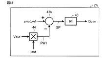
- FIG. 24 is a diagram showing a control block 158 which generates a command value Dpsc of the phase shift amount Dps.
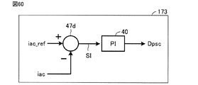
- the control block 158 includes a subtractor 39 a and a proportional control unit 40.
- the subtractor 39a calculates the difference current as a feedback amount by subtracting the output current iout detected by the second current detector 679 from the command value iout_ref of the output current output from the control block 157 of FIG. .
- the proportional control unit 40 outputs a command value Dpsc of the phase shift amount Dps by performing proportional control of the difference current.
- FIG. 25 is a diagram showing a control block 159 that generates a command value Dps_limitc of the control phase shift amount Dps_limit.
- the control block 159 comprises a comparator 41 and a multiplexer (MUX) 42.
- the comparator 41 compares the low duty ratio Dlimit calculated by the control block 156 of FIG. 22 with the command value Dpsc of the phase shift amount Dps calculated by the control block 158 of FIG. 24, and outputs a signal representing the comparison result. Do.
- the multiplexer (MUX) 42 receives the low duty ratio and the command value Dpsc.
- the multiplexer (MUX) 42 outputs one of the input signals as the command value Dps_limitc of the control phase shift amount Dps_limit according to the output signal of the comparator 41.
- control block 159 When the low duty ratio Dlimit is equal to or greater than the command value Dpsc, the output of the comparator 41 becomes high level.
- the multiplexer (MUX) 42 outputs the command value Dpsc as the command value Dps_limitc of the control phase shift amount Dps_limit.
- the output of the comparator 41 becomes low level.
- the multiplexer (MUX) 42 outputs the low duty ratio Dlimit as a command value Dps_limitc of the control phase shift amount Dps_limit.
- FIG. 26 is a diagram showing a control block 160 that generates a command value fs_ref of the switching frequency.
- the control block 160 includes a multiplier 44, a multiplier 45, a divider 46, a subtractor 47a, and a PI control unit 48.
- the multiplier 44 outputs an output power PW1 by multiplying the output voltage Vout obtained from the second voltage detector 676 by the output current iout obtained from the second current detector 679.
- the multiplier 45 multiplies the input power PW2 by multiplying the effective voltage Vac of the AC power supply 1 obtained from the third voltage detector 677 by the effective current Iac of the AC power supply 1 obtained from the first current detector 678. Output.
- the divider 46 outputs the conversion efficiency ⁇ by dividing the output power PW1 by the input power PW2.
- the subtractor 47a subtracts the predetermined target efficiency ⁇ ref and the conversion efficiency ⁇ output from the divider 46 to calculate the difference efficiency S ⁇ as a feedback amount.
- the PI control unit 48 performs proportional-plus-integral control of the difference efficiency S ⁇ and outputs a command value fs_ref of the switching frequency.
- the input power PW2 is active power in consideration of the input power factor.
- FIG. 27 is a diagram showing a control block 165 which generates gate signals g11 and g12 for semiconductor elements constituting the first leg 500. As shown in FIG.
- the control block 165 comprises a comparator 49 and a comparator 50.
- the comparator 49 compares the carrier wave having the frequency component of the command value fs_ref of the switching frequency with the command value D 502 c of the duty ratio D 502 calculated by the control block 153 of FIG.
- the level of the first gate signal g11 is set.
- the comparator 50 compares the command value D 502 c of the duty ratio D 502 calculated by the control block 153 of FIG. 19 with the carrier wave having the frequency component of the command value fs_ref of the switching frequency, and based on the comparison result, the first leg Set the level of the second gate signal g12 for
- the operation of the control block 165 will be described.
- the command value D 502 c of the duty ratio D 502 is smaller than the carrier wave having the frequency component of the command value fs_ref of the switching frequency
- the first gate signal g 11 for the first leg output by the comparator 49 becomes high level.
- the second gate signal g12 for the first leg that is output is at the low level.
- the first leg first gate signal g11 output by the comparator 49 becomes low level.
- the second gate signal g12 for the first leg that is output becomes high level.
- FIG. 28 is a diagram showing a control block 166 which generates gate signals g21 and g22 for semiconductor elements constituting the second leg 600. As shown in FIG.
- the control block 166 includes a comparator 51, a multiplexer (MUX) 52, an adder 53, a comparator 54, a comparator 55, an AND circuit 56, and a NOT circuit 57.
- MUX multiplexer
- the multiplexer (MUX) 52 outputs a command value D2c of the duty ratio of the second semiconductor element 502.
- the multiplexer (MUX) 52 outputs a command value D1c of the duty ratio of the first semiconductor element 501.
- the adder 53 adds the command value Dps_limitc of the control phase shift amount Dps_limit output from the control block 159 and the output value of the multiplexer (MUX) 52 to calculate an operation value.
- the comparator 54 compares the carrier wave having the frequency component of the command value fs_ref of the switching frequency calculated by the control block 160 with the command value Dps_limitc, and outputs a comparison result OP1.
- the comparator 54 compares the carrier wave having the frequency component of the command value fs_ref of the switching frequency calculated by the control block 160 with the output value of the adder 53, and outputs a comparison result OP2.
- the AND circuit 56 takes the logical product of the comparison result OP1 and the comparison result OP2 and outputs the second gate signal g22 for the second leg.
- the logical negation circuit 57 inverts the logical product of the comparison result OP1 and the comparison result OP2 and outputs the first gate signal g21 for the second leg.
- FIG. 29 is a diagram showing a control block 167 that generates a gate signal g1 of the first semiconductor element 501 and a gate signal g2 of the second semiconductor element 502.
- the control block 167 comprises a comparator 58, a multiplexer 59 and a multiplexer 61.
- the comparator 58 compares the voltage vac of the AC power supply 1 detected by the third voltage detector 677 with the ground voltage, and outputs a signal representing the comparison result.
- the multiplexer (MUX) 59 receives the first gate signal g11 for the first leg and the second gate signal g12 for the first leg.
- the multiplexer (MUX) 59 outputs one of the input gate signals as the gate signal g1 of the first semiconductor element 501 in accordance with the output signal of the comparator 58.
- the multiplexer (MUX) 61 receives the first gate signal g11 for the first leg and the second gate signal g12 for the first leg.
- the multiplexer (MUX) 61 outputs one of the input gate signals as the gate signal g2 of the second semiconductor element 502 in accordance with the output signal of the comparator 58.
- the operation of the control block 167 will be described.
- the output of the comparator 58 becomes high level.
- the multiplexer (MUX) 59 outputs the first gate signal g11 for the first leg as the gate signal g1 of the first semiconductor element 501.
- the multiplexer (MUX) 61 outputs the second gate signal g12 for the first leg as the gate signal g2 of the second semiconductor element 502.
- the output of the comparator 58 is at the low level.
- the multiplexer (MUX) 59 outputs the second gate signal g12 for the first leg as the gate signal g1 of the first semiconductor element 501.
- the multiplexer (MUX) 61 outputs the first gate signal g11 for the first leg as the gate signal g2 of the second semiconductor element 502.
- FIG. 30 is a diagram showing a control block 168 that generates a gate signal g3 of the third semiconductor element 601 and a gate signal g4 of the fourth semiconductor element 602.
- the control block 168 comprises a comparator 49, a multiplexer 64 and a multiplexer 65.
- the comparator 49 compares the voltage vac of the AC power supply 1 detected by the third voltage detector 677 with the ground voltage, and outputs a signal representing the comparison result.
- the multiplexer (MUX) 64 receives the first gate signal g21 for the second leg and the second gate signal g22 for the second leg.
- the multiplexer (MUX) 64 outputs one of the input gate signals as the gate signal g3 of the third semiconductor element 601 in accordance with the output signal of the comparator 49.
- the multiplexer (MUX) 66 receives the first gate signal g21 for the second leg and the second gate signal g22 for the second leg.
- the multiplexer (MUX) 66 outputs one of the input gate signals as the gate signal g4 of the fourth semiconductor element 602 in accordance with the output signal of the comparator 49.
- control block 168 The operation of control block 168 is described.
- the output of the comparator 49 is at the high level.
- the multiplexer (MUX) 64 outputs the first gate signal g21 for the second leg as the gate signal g3 of the third semiconductor element 601.
- the multiplexer (MUX) 66 outputs the second gate signal g22 for the second leg as the gate signal g4 of the fourth semiconductor element 602.
- the multiplexer (MUX) 64 outputs the second gate signal g22 for the second leg as the gate signal g3 of the third semiconductor element 601.
- the multiplexer (MUX) 66 outputs the first gate signal g 21 for the second leg as the gate signal g 4 of the fourth semiconductor element 602.
- FIG. 31 is a diagram showing a control block 169 that generates a command value fs_ref of the switching frequency.
- the control block 169 includes a subtractor 39 b and a proportional control unit 448.
- the subtractor 39b calculates a difference current as a feedback amount by subtracting the output current iout detected by the second current detector 679 from the command value iout_ref of the output current output from the control block 157 of FIG. .
- the proportional control unit 448 outputs a command value fs_ref of the switching frequency by performing proportional control of the difference current.
- FIG. 32 is a diagram showing a control block 175 that generates gate signals g21 and g22 for semiconductor elements that constitute the second leg 600. As shown in FIG.
- the control block 175 comprises a comparator 357 and a comparator 356.
- the comparator 357 compares the carrier wave having the frequency component of the command value fs_ref of the switching frequency with the command value D501c of the duty ratio D501 calculated by the control block 153 of FIG. And sets the level of the first gate signal g21.
- the comparator 356 compares the command value D501c of the duty ratio D501 calculated by the control block 153 of FIG. 19 with the carrier wave having the frequency component of the command value fs_ref of the switching frequency, and based on the comparison result, the second leg Set the level of the second gate signal g22 for
- control block 175 When the command value D501c of the duty ratio D501 is smaller than the carrier wave having the frequency component of the switching frequency command value fs_ref, the first leg gate signal g21 for the second leg output by the comparator 357 becomes high level, and the comparator 356 The second gate signal g22 for the second leg that is output becomes low level.
- the first gate signal g21 for the second leg output by the comparator 357 becomes low level.
- the second gate signal g22 for the second leg that is output becomes high level.
- FIG. 33 is a diagram showing a control block 176 which generates gate signals g11 and g12 for semiconductor elements constituting the first leg 500. As shown in FIG.
- Control block 176 includes a comparator 849 and a comparator 850.
- the comparator 849 compares the carrier wave having a fixed switching frequency component with the command value D502c of the duty ratio D502 calculated by the control block 153 of FIG. 1. Set the level of the gate signal g11.
- the comparator 850 compares the command value D 502 c of the duty ratio D 502 calculated by the control block 153 of FIG. 19 with the carrier wave having a fixed switching frequency component, and based on the comparison result, the first for the first leg. 2. Set the level of the gate signal g12.
- control block 176 When the command value D502c of the duty ratio D502 is smaller than the carrier wave having the fixed switching frequency fs0 frequency component, the first leg first gate signal g11 output by the comparator 849 becomes high level, and the comparator 850 The second gate signal g12 for the first leg to be output is at the low level.
- FIG. 34 is a diagram showing a control block 177 which generates gate signals g21 and g22 for semiconductor elements constituting the second leg 600. As shown in FIG.
- the control block 177 includes a comparator 851, a multiplexer (MUX) 852, an adder 853, a comparator 854, a comparator 855, an AND circuit 856, and an negation circuit 857.
- MUX multiplexer
- the multiplexer (MUX) 852 outputs a command value D2c of the duty ratio of the second semiconductor element 502.
- the output of the comparator 851 is at the low level.
- the multiplexer (MUX) 852 outputs a command value D1c of the duty ratio of the first semiconductor element 501.
- the adder 853 adds the command value Dps_limitc of the control phase shift amount Dps_limit output from the control block 159 and the output value of the multiplexer (MUX) 852 to calculate an operation value.
- the comparator 854 compares the carrier wave having a fixed frequency component of the switching frequency with the command value Dps_limitc, and outputs a comparison result OP1.
- the comparator 855 compares the carrier wave having the frequency component of the command value fs_ref of the fixed switching frequency with the output value of the adder 853 and outputs a comparison result OP2.
- the AND circuit 856 takes the logical product of the comparison result OP1 and the comparison result OP2 and outputs the second gate signal g22 for the second leg.
- the logical negation circuit 857 inverts the logical product of the comparison result OP1 and the comparison result OP2 and outputs the first gate signal g21 for the second leg.
- high power factor control and output control are simultaneously performed with one full bridge inverter circuit by simultaneously using at least one of frequency modulation control and phase shift control in addition to pulse frequency modulation control.
- frequency modulation control and phase shift control in addition to pulse frequency modulation control.
- FIG. 35 is a diagram showing a control method in the first modification of the first embodiment.
- the control circuit 14 controls the first leg 500, the second leg 600, and the third leg 300 based on the third control method in a region where the target value M * of the voltage conversion ratio M is larger than the threshold TH1.
- the control circuit 14 controls the first leg 500 by pulse width modulation control.
- the control circuit 14 controls the second leg 600 by pulse width modulation control and phase shift modulation control.
- the control circuit 14 controls the third leg 300 to perform rectification.
- the control circuit 14 controls the first leg 500, the second leg 600, and the third leg 300 based on the second control method in a region where the target value M * of the voltage conversion ratio M is less than or equal to the threshold TH1 and greater than the threshold TH2. Control.
- the control circuit 14 controls the first leg 500 by pulse width modulation control and pulse frequency modulation control.
- the control circuit 14 controls the second leg 600 by pulse width modulation control, pulse frequency modulation control, and phase shift modulation.
- the control circuit 14 controls the third leg 300 to perform rectification.
- the control circuit 14 controls the first leg 500, the second leg 600, and the third leg 300 based on the first control method in a region where the target value M * of the voltage conversion ratio M is less than or equal to the threshold TH2.
- the control circuit 14 controls the first leg 500 by pulse width modulation control and pulse frequency control.
- the control circuit 14 controls the second leg 600 by pulse width modulation control and pulse frequency modulation control.
- the control circuit 14 controls the third leg 300 to perform rectification.
- FIG. 36 is a diagram showing a control method in the second modification of the first embodiment.
- the control circuit 14 controls the first leg 500, the second leg 600, and the third leg 300 based on the first control method in a region where the target value M * of the voltage conversion ratio M is larger than the threshold TH.
- the control circuit 14 controls the first leg 500 by pulse width modulation control and pulse frequency modulation control.
- the control circuit 14 controls the second leg 600 by pulse width modulation control and pulse frequency modulation control.
- the control circuit 14 controls the third leg 300 to perform rectification.
- the control circuit 14 controls the first leg 500, the second leg 600, and the third leg 300 based on the second control method in a region where the target value M * of the voltage conversion ratio M is less than or equal to the threshold TH.
- the control circuit 14 controls the first leg 500 by pulse width modulation control and pulse frequency modulation control.
- the control circuit 14 controls the second leg 600 by pulse width modulation control, pulse frequency modulation control, and phase shift modulation.
- the control circuit 14 controls the third leg 300 to perform rectification.
- FIG. 37 is a diagram showing a control method in the third modification of the first embodiment.
- the control circuit 14 controls the first leg 500, the second leg 600, and the third leg 300 based on the second control method in a region where the target value M * of the voltage conversion ratio M is larger than the threshold TH.
- the control circuit 14 controls the first leg 500 by pulse width modulation control and pulse frequency modulation control.
- the control circuit 14 controls the second leg 600 by pulse width modulation control, pulse frequency modulation control, and phase shift modulation.
- the control circuit 14 controls the third leg 300 to perform rectification.
- the control circuit 14 controls the first leg 500, the second leg 600, and the third leg 300 based on the third control method in a region where the target value M * of the voltage conversion ratio M is less than or equal to the threshold TH.
- the control circuit 14 controls the first leg 500 by pulse width modulation control.
- the control circuit 14 controls the second leg 600 by pulse width modulation control and phase shift modulation.
- the control circuit 14 controls the third leg 300 to perform rectification.
- circuit configuration of the power conversion device in the present embodiment is substantially the same as the case shown in the first embodiment, and thus the detailed description of the configuration will not be repeated.
- the first semiconductor element 501 and the second semiconductor element 502 constituting the first leg 500, and the fifth semiconductor element 301 and the sixth semiconductor element 302 constituting the third leg 300 have high power factor control.
- the output of the third semiconductor element 601 and the fourth semiconductor element constituting the second leg 600 is controlled.
- FIG. 38 is a diagram showing a control method in the second embodiment.
- the control circuit 14 controls the first leg 500, the second leg 600, and the third leg 300 based on the fourth control method in a region where the target value M * of the voltage conversion ratio M is larger than the threshold TH1.
- the control circuit 14 controls the first leg 500 by pulse width modulation control and pulse frequency modulation control.
- the control circuit 14 controls the second leg 600 by pulse width modulation control and pulse frequency modulation control.
- the control circuit 14 controls the third leg 300 by pulse width modulation control and pulse frequency modulation control.
- the control circuit 14 controls the first leg 500, the second leg 600, and the third leg 300 based on the fifth control method in a region where the target value M * of the voltage conversion ratio M is less than or equal to the threshold TH1 and greater than the threshold TH2. Control.
- the control circuit 14 controls the first leg 500 by pulse width modulation control and pulse frequency modulation control.
- the control circuit 14 controls the second leg 600 by pulse width modulation control, pulse frequency modulation control, and phase shift modulation.
- the control circuit 14 controls the third leg 300 by pulse width modulation control and pulse frequency modulation control.
- the control circuit 14 controls the first leg 500, the second leg 600, and the third leg 300 based on the sixth control method in a region where the target value M * of the voltage conversion ratio M is less than or equal to the threshold TH2.
- the control circuit 14 controls the first leg 500 by pulse width modulation control.
- the control circuit 14 controls the second leg 600 by pulse width modulation control and phase shift modulation control.
- the control circuit 14 controls the third leg 300 by pulse width modulation control.
- (4th control method) 39 shows gate pulses of the first semiconductor element 501, the second semiconductor element 502, the third semiconductor element 601, the fourth semiconductor element 602, the fifth semiconductor element 301, and the sixth semiconductor element 302 in the fourth control method. It is a figure showing an example.
- the pulse of the first semiconductor element 501 and the pulse of the sixth semiconductor element 302 are synchronized, and the pulse of the second semiconductor element 502 and the pulse of the fifth semiconductor element 301 are synchronized. Furthermore, the timing when the first semiconductor element 501 turns on and the timing when the sixth semiconductor element 302 turns on synchronize with the timing when the fourth semiconductor element 602 turns on, and the timing when the second semiconductor element 502 turns off and the fifth semiconductor. The timing at which the element 301 is turned off and the timing at which the third semiconductor element 601 is turned off are synchronized.
- the pulse width of the first semiconductor element 501, the pulse width of the third semiconductor element 601, and the pulse width of the sixth semiconductor element 302 are equal, and the pulse width of the second semiconductor element 502 and the pulse width of the fourth semiconductor element 602. And the pulse width of the fifth semiconductor element 301 are equal.
- the control circuit 14 satisfies the above conditions while the first semiconductor element 501, the second semiconductor element 502, the third semiconductor element 601, the fourth semiconductor element 602, the fifth semiconductor element 301, and the sixth semiconductor element 302.
- the first semiconductor element 501, the second semiconductor element 502, the third semiconductor element 601, the fourth semiconductor element 602, the fifth semiconductor element 301, and the sixth semiconductor element 302 are controlled such that the common switching frequency fs changes. .
- FIG. 40 shows gate pulses of the first semiconductor device 501, the second semiconductor device 502, the third semiconductor device 601, the fourth semiconductor device 602, the fifth semiconductor device 301, and the sixth semiconductor device 302 in the fourth control method. It is a figure showing another example.
- the pulse of the first semiconductor element 501 and the pulse of the sixth semiconductor element 302 are synchronized, and the pulse of the second semiconductor element 502 and the pulse of the fifth semiconductor element 301 are synchronized. Furthermore, the central phase of the gate pulse of the first semiconductor element 501, the central phase of the gate pulse of the fourth semiconductor element 602, and the central phase of the gate pulse of the sixth semiconductor element 302 are synchronized, and the second semiconductor element 502. The central phase of the gate pulse of the third semiconductor element 601 and the central phase of the gate pulse of the fifth semiconductor element 301 are synchronized with each other.
- the pulse width of the first semiconductor element 501, the pulse width of the third semiconductor element 601, and the pulse width of the sixth semiconductor element 302 are equal, and the pulse width of the second semiconductor element 502 and the pulse width of the fourth semiconductor element 602. And the pulse width of the fifth semiconductor element 301 are equal.
- the control circuit 14 satisfies the above conditions while the first semiconductor element 501, the second semiconductor element 502, the third semiconductor element 601, the fourth semiconductor element 602, the fifth semiconductor element 301, and the sixth semiconductor element 302.
- the first semiconductor element 501, the second semiconductor element 502, the third semiconductor element 601, the fourth semiconductor element 602, the fifth semiconductor element 301, and the sixth semiconductor element 302 are controlled such that the common switching frequency fs changes. .
- the length of the period when the first semiconductor element 501 and the fourth semiconductor element 602 located at the diagonal are simultaneously turned on and the second semiconductor element 502 and the third located at the diagonal Since the length of the period during which the semiconductor element 601 is simultaneously turned on can be made the same, stable power supply becomes possible.
- (Sixth control method) 41 shows gate pulses of the first semiconductor element 501, the second semiconductor element 502, the third semiconductor element 601, the fourth semiconductor element 602, the fifth semiconductor element 301, and the sixth semiconductor element 302 in the sixth control method. It is a figure showing another example.
- the pulse of the first semiconductor element 501 and the pulse of the sixth semiconductor element 302 are synchronized, and the pulse of the second semiconductor element 502 and the pulse of the fifth semiconductor element 301 are synchronized. Furthermore, in the initial state of phase shift control, the timing at which the first semiconductor element 501 is turned on, the timing at which the fourth semiconductor element 602 is turned on, and the timing at which the sixth semiconductor element 302 is turned on are synchronized. It is defined that the timing at which the second semiconductor device 601 turns off and the timing at which the third semiconductor device 601 turns off are synchronized with the timing at which the fifth semiconductor device 301 turns on. From this initial state, the phase of the third semiconductor element 601 and the phase of the fourth semiconductor element 602 shift.
- the pulse width of the first semiconductor element 501, the pulse width of the third semiconductor element 601, and the pulse width of the sixth semiconductor element 302 are equal, and the pulse width of the second semiconductor element 502, the fourth semiconductor element 602. And the pulse width of the fifth semiconductor element 301 are equal.
- the control circuit 14 performs the first semiconductor element 501, the second semiconductor element 502, the third semiconductor element 601, the fourth semiconductor element 602, the fifth semiconductor element 301, and the sixth semiconductor element 302 so as to satisfy such conditions. Control.
- the pulse of the first semiconductor element 501 and the pulse of the sixth semiconductor element 302 are synchronized, and the pulse of the second semiconductor element 502 and the pulse of the fifth semiconductor element 301 are synchronized.
- the timing when the first semiconductor element 501 is turned on, the timing when the third semiconductor element 601 is turned on, and the timing when the sixth semiconductor element 302 is turned on are synchronized.
- a state in which the timing when the element 502 is turned on, the timing when the fourth semiconductor element 602 is turned on, and the timing when the fifth semiconductor element 301 is turned on is synchronized is defined. From this initial state, the phase of the third semiconductor element 601 and the phase of the fourth semiconductor element 602 shift.
- the pulse width of the first semiconductor element 501, the pulse width of the third semiconductor element 601, and the pulse width of the sixth semiconductor element 302 are equal, and the pulse width of the second semiconductor element 502, the fourth semiconductor element 602. And the pulse width of the fifth semiconductor element 301 are equal.
- the control circuit 14 performs the first semiconductor element 501, the second semiconductor element 502, the third semiconductor element 601, the fourth semiconductor element 602, the fifth semiconductor element 301, and the sixth semiconductor element 302 so as to satisfy such conditions. Control.
- the length of the period when the first semiconductor element 501 and the fourth semiconductor element 602 located at the diagonal are simultaneously turned on and the second semiconductor element 502 and the third located at the diagonal Since the length of the period during which the semiconductor element 601 is simultaneously turned on can be made the same, stable power supply becomes possible.
- (Fifth control method) 43 shows gate pulses of the first semiconductor element 501, the second semiconductor element 502, the third semiconductor element 601, the fourth semiconductor element 602, the fifth semiconductor element 301, and the sixth semiconductor element 302 in the fifth control method. It is a figure showing an example.
- the pulse of the first semiconductor element 501 and the pulse of the sixth semiconductor element 302 are synchronized, and the pulse of the second semiconductor element 502 and the pulse of the fifth semiconductor element 301 are synchronized.
- the timing at which the first semiconductor element 501 is turned on, the timing at which the fourth semiconductor element 602 is turned on, and the timing at which the sixth semiconductor element 302 is turned on are synchronized. It is defined that the timing at which the second semiconductor device 601 turns off and the timing at which the third semiconductor device 601 turns off are synchronized with the timing at which the fifth semiconductor device 301 turns on. From this initial state, the phase of the third semiconductor element 601 and the phase of the fourth semiconductor element 602 shift.
- the pulse width of the first semiconductor element 501, the pulse width of the third semiconductor element 601, and the pulse width of the sixth semiconductor element 302 are equal, and the pulse width of the second semiconductor element 502, the fourth semiconductor element 602. And the pulse width of the fifth semiconductor element 301 are equal.
- the control circuit 14 satisfies the above conditions while the first semiconductor element 501, the second semiconductor element 502, the third semiconductor element 601, the fourth semiconductor element 602, the fifth semiconductor element 301, and the sixth semiconductor element 302.
- the first semiconductor element 501, the second semiconductor element 502, the third semiconductor element 601, the fourth semiconductor element 602, the fifth semiconductor element 301, and the sixth semiconductor element 302 are controlled such that the common switching frequency fs changes. .
- the pulse of the first semiconductor element 501 and the pulse of the sixth semiconductor element 302 are synchronized, and the pulse of the second semiconductor element 502 and the pulse of the fifth semiconductor element 301 are synchronized.
- the timing when the first semiconductor element 501 is turned on, the timing when the third semiconductor element 601 is turned on, and the timing when the sixth semiconductor element 302 is turned on are synchronized.
- a state in which the timing when the element 502 is turned on, the timing when the fourth semiconductor element 602 is turned on, and the timing when the fifth semiconductor element 301 is turned on is synchronized is defined. From this initial state, the phase of the third semiconductor element 601 and the phase of the fourth semiconductor element 602 shift.
- the pulse width of the first semiconductor element 501, the pulse width of the third semiconductor element 601, and the pulse width of the sixth semiconductor element 302 are equal, and the pulse width of the second semiconductor element 502, the fourth semiconductor element 602. And the pulse width of the fifth semiconductor element 301 are equal.
- the control circuit 14 satisfies the above conditions while the first semiconductor element 501, the second semiconductor element 502, the third semiconductor element 601, the fourth semiconductor element 602, the fifth semiconductor element 301, and the sixth semiconductor element 302.
- the first semiconductor element 501, the second semiconductor element 502, the third semiconductor element 601, the fourth semiconductor element 602, the fifth semiconductor element 301, and the sixth semiconductor element 302 are controlled such that the common switching frequency fs changes. .
- the length of the period when the first semiconductor element 501 and the fourth semiconductor element 602 located at the diagonal are simultaneously turned on and the second semiconductor element 502 and the third located at the diagonal Since the length of the period during which the semiconductor element 601 is simultaneously turned on can be made the same, stable power supply becomes possible.
- FIG. 45 shows a plurality of control blocks responsible for the fourth control method.
- the difference between the plurality of control blocks of the fourth control method and the plurality of control blocks responsible for the first control method of the first embodiment is that in the plurality of control blocks of the fourth control method, the control block 167 is used.
- Control block 178 is included instead.
- the control block 178 outputs the first gate signal g11 for the first leg as the gate signal g1 of the first semiconductor element 501 and the gate signal g6 of the sixth semiconductor element 302 when the voltage vac of the AC power supply 1 is positive.
- the second gate signal g12 for the first leg is output as the gate signal g2 of the second semiconductor element 502 and the gate signal g5 of the fifth semiconductor element 301.
- the control block 167 outputs the second gate signal g12 for the first leg as the gate signal g1 of the first semiconductor element 501 and the gate signal g6 of the sixth semiconductor element 302 when the voltage vac of the AC power supply 1 is negative.
- the first gate signal g11 for the first leg is output as the gate signal g2 of the second semiconductor element 502 and the gate signal g5 of the fifth semiconductor element 301.
- FIG. 46 is a diagram showing a plurality of control blocks responsible for the sixth control method.
- the plurality of control blocks of the sixth control method is different from the plurality of control blocks in the first control method of the first embodiment in that the control blocks of the sixth control method are different from the control blocks 167.
- Control block 178 is included instead.
- the control block 178 is similar to the control block 178 of the fourth control scheme, so the description will not be repeated.
- FIG. 47 is a diagram showing a plurality of control blocks responsible for the fifth control method.
- the difference between the plurality of control blocks of the fifth control method and the plurality of control blocks responsible for the second control method of the first embodiment is that the control block 167 of the fifth control method Control block 178 is included instead.
- the control block 178 is similar to the control block 178 of the fourth control scheme, so the description will not be repeated.
- FIG. 48 generates a gate signal g1 of the first semiconductor element 501, a gate signal g2 of the second semiconductor element 502, a gate signal g5 of the fifth semiconductor element 301, and a gate signal g6 of the sixth semiconductor element 302.
- FIG. 7 is a diagram illustrating a control block 178.
- the control block 178 comprises a comparator 58, a multiplexer 59 and a multiplexer 61.
- the comparator 58 compares the voltage vac of the AC power supply 1 detected by the third voltage detector 677 with the ground voltage, and outputs a signal representing the comparison result.
- the multiplexer (MUX) 59 receives the first gate signal g11 for the first leg and the second gate signal g12 for the first leg.
- the multiplexer (MUX) 59 outputs one of the input gate signals as the gate signal g 1 of the first semiconductor element 501 and the gate signal g 6 of the sixth semiconductor element 302 in accordance with the output signal of the comparator 58.
- the multiplexer (MUX) 61 receives the first gate signal g11 for the first leg and the second gate signal g12 for the first leg.
- the multiplexer (MUX) 61 outputs one of the input gate signals as the gate signal g 2 of the second semiconductor element 502 and the gate signal g 5 of the fifth semiconductor element 301 in accordance with the output signal of the comparator 58.
- control block 178 When the voltage vac of the alternating current power supply 1 obtained from the third voltage detector 677 that detects the voltage of the alternating current power supply 1 is positive, the output of the comparator 58 becomes high level.
- the multiplexer (MUX) 59 outputs the first gate signal g11 for the first leg as the gate signal g1 of the first semiconductor element 501 and the gate signal g6 of the sixth semiconductor element 302.
- the multiplexer (MUX) 61 outputs the second gate signal g12 for the first leg as the gate signal g2 of the second semiconductor element 502 and the gate signal g5 of the fifth semiconductor element 301.
- the multiplexer (MUX) 59 outputs the second gate signal g12 for the first leg as the gate signal g1 of the first semiconductor element 501 and the gate signal g6 of the sixth semiconductor element 302.
- the multiplexer (MUX) 61 outputs the first gate signal g11 for the first leg as the gate signal g2 of the second semiconductor element 502 and the gate signal g5 of the fifth semiconductor element 301.
- the power loss is locally generated by sharing the power loss between the first semiconductor element 501, the second semiconductor element 502, the fifth semiconductor element 301, and the sixth semiconductor element 302. It becomes possible to operate so as not to. Further, in the present embodiment, since the above-described circuit configuration and control method are used, high power factor control and wide-area control can be performed with a single-stage full bridge inverter circuit, as in the power conversion device shown in the first embodiment. It becomes possible to perform output control simultaneously.
- FIG. 49 is a diagram showing a control method in the first modification of the second embodiment.
- the control circuit 14 controls the first leg 500, the second leg 600, and the third leg 300 based on the sixth control method in a region where the target value M * of the voltage conversion ratio M is larger than the threshold TH1.
- the control circuit 14 controls the first leg 500 by pulse width modulation control.
- the control circuit 14 controls the second leg 600 by pulse width modulation control and phase shift modulation control.
- the control circuit 14 controls the third leg 300 by pulse width modulation control.
- the control circuit 14 controls the first leg 500, the second leg 600, and the third leg 300 based on the fifth control method in a region where the target value M * of the voltage conversion ratio M is less than or equal to the threshold TH1 and greater than the threshold TH2. Control.
- the control circuit 14 controls the first leg 500 by pulse width modulation control and pulse frequency modulation control.
- the control circuit 14 controls the second leg 600 by pulse width modulation control, pulse frequency modulation control, and phase shift modulation.
- the control circuit 14 controls the third leg 300 by pulse width modulation control and pulse frequency modulation control.
- the control circuit 14 controls the first leg 500, the second leg 600, and the third leg 300 based on the fourth control method in a region where the target value M * of the voltage conversion ratio M is less than or equal to the threshold TH2.
- the control circuit 14 controls the first leg 500 by pulse width modulation control and pulse frequency control.
- the control circuit 14 controls the second leg 600 by pulse width modulation control and pulse frequency modulation control.
- the control circuit 14 controls the third leg 300 by pulse width modulation control and pulse frequency control.
- FIG. 50 is a diagram showing a control method in the second modification of the second embodiment.
- the control circuit 14 controls the first leg 500, the second leg 600, and the third leg 300 based on the fourth control method in a region where the target value M * of the voltage conversion ratio M is larger than the threshold TH.
- the control circuit 14 controls the first leg 500 by pulse width modulation control and pulse frequency modulation control.
- the control circuit 14 controls the second leg 600 by pulse width modulation control and pulse frequency modulation control.
- the control circuit 14 controls the third leg 300 by pulse width modulation control and pulse frequency modulation control.
- the control circuit 14 controls the first leg 500, the second leg 600, and the third leg 300 based on the fifth control method in a region where the target value M * of the voltage conversion ratio M is less than or equal to the threshold TH.
- the control circuit 14 controls the first leg 500 by pulse width modulation control and pulse frequency modulation control.
- the control circuit 14 controls the second leg 600 by pulse width modulation control, pulse frequency modulation control, and phase shift modulation.
- the control circuit 14 controls the third leg 300 by pulse width modulation control and pulse frequency modulation control.
- FIG. 51 is a diagram illustrating a control method in the third modification of the second embodiment.
- the control circuit 14 controls the first leg 500, the second leg 600, and the third leg 300 based on the fifth control method in a region where the target value M * of the voltage conversion ratio M is larger than the threshold TH.
- the control circuit 14 controls the first leg 500 by pulse width modulation control and pulse frequency modulation control.
- the control circuit 14 controls the second leg 600 by pulse width modulation control, pulse frequency modulation control, and phase shift modulation.
- the control circuit 14 controls the third leg 300 by pulse width modulation control and pulse frequency modulation control.
- the control circuit 14 controls the first leg 500, the second leg 600, and the third leg 300 based on the sixth control method in a region where the target value M * of the voltage conversion ratio M is less than or equal to the threshold TH.
- the control circuit 14 controls the first leg 500 by pulse width modulation control.
- the control circuit 14 controls the second leg 600 by pulse width modulation control and phase shift modulation.
- the control circuit 14 controls the third leg 300 by pulse width modulation control.
- FIG. 52 is a diagram showing a configuration of a power conversion device 6000 of a modification.
- the fifth semiconductor element 301 and the sixth semiconductor element 302 are constituted by diodes which are passive semiconductors.
- One end of the AC power supply 1 is connected via the power factor improving reactor 2 to a first AC end ND1 to which the first semiconductor element 501 and the second semiconductor element 502 are connected.
- the first AC end ND1 is connected to the series resonance reactor 7.
- DC capacitor 4 smooths only the charge / discharge ripple due to switching period Ts. Just do it. As a result, the capacitance of the DC capacitor 4 can be significantly reduced as compared with the general method, and the DC capacitor 4 can be miniaturized.
- the control logic for generating command value fs_ref for the switching frequency is not limited to the control block 160 of FIG. 26, and other control logic may be used. It is good.
- FIG. 53 is a diagram showing a control block 161 that generates a command value fs_ref of the switching frequency.
- the multiplier 44 multiplies the output voltage Vout obtained from the second voltage detector 676 by the output current iout obtained from the second current detector 679 to output an output power PW1.
- the subtractor 47b calculates a difference power SP1 between a predetermined target value Pout_ref of output power and the output power PW1.
- the calculated difference power SP1 is input to the PI control unit 48 as a feedback amount.
- the PI control unit 48 performs proportional integral control of the difference power SP1 and outputs a command value fs_ref of the switching frequency.
- FIG. 54 is a diagram showing a control block 162 which generates a command value fs_ref of the switching frequency.
- the multiplier 44 multiplies the effective voltage Vac of the alternating current power supply 1 obtained from the third voltage detector 677 by the effective current Iac of the alternating current power supply 1 obtained from the first current detector 678 to obtain the power of the alternating current power supply 1. That is, the input power PW2 is calculated.
- the subtractor 47c calculates a difference power SP2 between a predetermined target value Pac_ref of the input power and the input power PW2.
- the calculated difference power SP2 is input to the PI control unit 48 as a feedback amount.
- the PI control unit 48 performs proportional integral control on the difference power SP2 and outputs a command value fs_ref of the switching frequency.
- the input power PW2 is active power in consideration of the input power factor.
- FIG. 55 is a diagram showing a control block 163 which generates a command value fs_ref of the switching frequency.
- the subtractor 47 d calculates a difference current SI 1 between a predetermined target current effective value Iac_ref of the AC power supply 1 and an effective current Iac of the AC power supply 1 obtained from the first current detector 678.
- the calculated difference current SI1 is input to the PI control unit 48 as a feedback amount.
- the PI control unit 48 performs proportional-plus-integral control of the difference current SI1, and outputs a command value fs_ref of the switching frequency.
- the effective current of the AC power supply 1 represents the input current.
- FIG. 56 is a diagram representing control block 164 for generating switching frequency command value fs_ref.
- the subtractor 47e calculates a difference current SI2 between the predetermined target value iout_ref of the output current and the output current iout obtained from the second current detector 679.
- the calculated difference current SI2 is input to the PI control unit 48 as a feedback amount.
- the PI control unit 48 performs proportional-integral control of the difference current SI2, and outputs a command value fs_ref of the switching frequency.
- Control logic for generating command value Dpsc of phase shift amount Dps is not limited to the control block 158 of FIG. You may use.
- FIG. 57 is a diagram showing control block 170 generating command value Dpsc of phase shift amount Dps.
- Control block 170 includes a multiplier 844, a multiplier 845, a divider 846, a subtractor 847 a, and a PI control unit 848.
- the multiplier 844 outputs an output power PW1 by multiplying the output voltage Vout obtained from the second voltage detector 676 by the output current iout obtained from the second current detector 679.
- the multiplier 845 multiplies the input voltage PW2 by multiplying the effective voltage Vac of the AC power supply 1 obtained from the third voltage detector 677 by the effective current Iac of the AC power supply 1 obtained from the first current detector 678. Output.
- the divider 846 outputs the conversion efficiency ⁇ by dividing the output power PW1 by the input power PW2.
- the subtractor 847a subtracts the predetermined target efficiency ⁇ ref and the conversion efficiency ⁇ output from the divider 46 to calculate the difference efficiency S ⁇ as a feedback amount.
- PI control unit 848 performs proportional-plus-integral control of difference efficiency S ⁇ , and outputs command value Dpsc of phase shift amount Dps.
- the input power PW2 is active power in consideration of the input power factor.
- FIG. 58 is a diagram showing a control block 171 which generates a command value Dpsc of the phase shift amount Dps.
- the control block 171 includes a multiplier 44, a subtractor 47b, and a PI control unit 40.
- the multiplier 44 outputs an output power PW1 by multiplying the output voltage Vout obtained from the second voltage detector 676 by the output current iout obtained from the second current detector 679.
- the subtractor 47b subtracts the predetermined target output power pout_ref and the output power PW1 output from the multiplier 44 to calculate a difference power SPwp as a feedback amount.
- the PI control unit 40 performs proportional integral control of the difference power SP, and outputs a command value Dpsc of the phase shift amount Dps.
- FIG. 59 is a diagram showing a control block 172 which generates a command value Dpsc of the phase shift amount Dps.
- the control block 172 includes a multiplier 45, a subtractor 47c, and a PI control unit 40.
- the multiplier 45 outputs AC power PW2 by multiplying the voltage vac of the AC power supply 1 obtained from the third voltage detector 677 by the current iac of the AC power supply 1 obtained from the first current detector 678. .
- the input power PW2 is active power in consideration of the input power factor.
- the subtractor 47c subtracts the predetermined target AC power pac_ref and the AC power PW2 output from the multiplier 45 to calculate the difference power SP as a feedback amount.
- the PI control unit 40 performs proportional integral control of the difference power SP, and outputs a command value Dpsc of the phase shift amount Dps.
- FIG. 60 is a diagram showing a control block 173 which generates a command value Dpsc of the phase shift amount Dps.
- the control block 173 includes a subtractor 47 d and a PI control unit 40.
- the subtractor 47 d subtracts the predetermined alternating current iac_ref and the current iac of the alternating current power source 1 obtained from the first current detector 678 to calculate a difference current SI as a feedback amount.
- the PI control unit 40 performs a proportional integral control on the difference current SI, and outputs a command value Dpsc of the phase shift amount Dps.
- FIG. 61 is a diagram showing a control block 174 that generates a command value Dpsc of the phase shift amount Dps.
- the control block 174 includes a subtractor 47 e and a PI control unit 40.
- the subtractor 47e calculates a difference current SI as a feedback amount by subtracting a predetermined output current iout_ref and an output current iout obtained from the second current detector 679.
- the PI control unit 40 performs a proportional integral control on the difference current SI, and outputs a command value Dpsc of the phase shift amount Dps.
- (4) Control Based on Efficiency The control block 160 generates a command value fs_ref of the switching frequency so that the efficiency calculated from the detected voltage and current follows the target efficiency, and the control block 170 calculates from the detected voltage and current
- the command value Dpsc of the phase shift amount Dps is generated so that the obtained efficiency follows the target efficiency, but the control method based on the efficiency is not limited to this.
- FIG. 62 is a diagram for describing a method of selecting the switching frequency fs and the phase shift amount Dps.
- a combination of a switching frequency fs capable of obtaining a desired voltage conversion ratio and a phase shift amount Dps is stored in a plurality of patterns, and is converged to the operation condition of the combination of which the conversion efficiency is largest. It is good.
- a combination of the switching frequency and the phase shift amount Dps may be stored continuously, or as shown in FIG. 62, the combination may be stored for each change width ⁇ fs of the switching frequency set arbitrarily. good.
- the conversion efficiency may be stored, but also a combination in which the output power is maximized may be stored, a combination in which the input power is maximized may be stored, or even a combination in which the input current is maximized is stored You may store the combination which becomes good and output current becomes the largest.
- Secondary side rectifier circuit 11 The secondary side rectifier circuit 11 is not limited to the configuration shown in FIG.
- FIG. 63 is a diagram showing a modification of secondary side rectifier circuit 11.
- the transformer 9 may be a center tap type, and a center tap diode rectification system using a diode as a semiconductor element may be used.
- FIG. 64 is a diagram showing another modification of the secondary side rectifier circuit 11.
- one of the two legs may be configured by two diodes, and the other may be configured by two capacitors.
- FIG. 65 is a diagram showing another modification of the secondary side rectifier circuit 11.
- a full bridge synchronous rectification system may be employed in which a full bridge is configured of four active semiconductors.
- FIG. 66 is a diagram showing another modification of the secondary side rectifier circuit 11.
- a center tap synchronous rectification system may be adopted in which the active element is used for the semiconductor element with the transformer 9 as the center tap type.
- FIG. 67 is a diagram showing another modification of the secondary side rectifier circuit 11.
- a voltage doubled synchronous rectification system may be employed in which one of the two legs is composed of two active semiconductors, and the other is composed of two capacitors.
- FIG. 68 is a diagram showing a modification of output smoothing circuit 1200.
- the configuration of the output smoothing circuit 1200 may be a capacitor input method in which smoothing is performed using only the capacitor C.
- FIG. 69 shows another modification of output smoothing circuit 1200.
- the configuration of the output smoothing circuit 1200 may adopt a smoothing method in which a plurality of capacitors C1, C2, C3 and inductors L1, L2 are alternately connected.
- the number of capacitors and inductors is not limited to this.
- Second voltage detector 676 The second voltage detector that detects the output voltage Vout is not limited to the method of detecting the voltage of the second output smoothing capacitor 1203 described in FIG. 1, but detects the voltage of the first output smoothing capacitor 1201. The voltage of the DC load 13 may be detected.
- output smoothing circuit 1200 has the configuration shown in FIG. 68 or 69, either one of the method of detecting the capacitor voltage or the method of detecting the voltage of DC load 13 may be selected.
- Second current detector 679 The second current detector for detecting the output current iout is not limited to a point connected in series with the DC load 13 as shown in FIG. 1, and may be arranged in a point connected in series with the output smoothing reactor 1202 The current of reactor 1202 may be detected.
- Control Block The control block included in the control circuit may be configured by hardware using an arithmetic circuit.
- FIG. 70 shows a modification of control circuit 14. Referring to FIG. As shown in FIG. 70, it may be configured as software using a memory 746 for storing a program and a processor 745 for processing the program.
- the series resonance reactor 7 may be substituted by the leakage inductance of the transformer 9, and the parallel resonance reactor 8 may be substituted by the excitation inductance of the transformer 9.
- the series resonance reactor 7, the parallel resonance reactor 8, and the series resonance capacitor 10 are disposed on the primary side of the transformer 9, but may be disposed on the secondary side of the transformer 9. Alternatively, it may be distributed to each of the primary side and the secondary side of the transformer 9.
- the series resonance reactor 7 and the series resonance capacitor 10 are connected to any of the primary side terminals of the transformer 9, they may be dispersed to both side terminals, and the secondary of the transformer 9 It may be distributed to both side terminals on the side.
- control block 160 a control block 169 may be used.
- the CP control mode may be controlled as follows.
- the first leg 500 switches on-period to follow a target sine wave current in phase with the sine wave voltage obtained from the third voltage detector 677 based on the value obtained from the first current detector 678, and High power factor control is performed by adjusting the frequency.
- the second leg 600 performs output control by adjusting the ON period and the switching frequency so as to follow the target DC voltage based on the value obtained from the first voltage detector 675.
- control may be performed as follows.
- the first leg 500 follows the DC voltage of the DC capacitor 4 to the target DC voltage based on the values obtained from the first voltage detector 675, the third voltage detector 677, and the first current detector 678.
- high power factor control is performed by adjusting the on period and the switching frequency.
- the second leg 600 performs output control by adjusting the on period and the frequency to follow the target DC current based on the value obtained from the second current detector 679.
- control in the fourth control method, in the CP control mode, control may be performed as follows.
- the first leg 500 and the third leg are turned on to follow the target sine wave current in phase with the sine wave voltage obtained from the third voltage detector 677 based on the value obtained from the first current detector 678.
- High power factor control is performed by adjusting the period and the switching frequency.
- the second leg 600 performs output control by adjusting the ON period and the switching frequency so as to follow the target DC voltage based on the value obtained from the first voltage detector 675.
- control may be performed as follows.
- the first leg 500 and the third leg target the DC voltage of the DC capacitor 4 based on the values obtained from the first voltage detector 675, the third voltage detector 677, and the first current detector 678.
- High power factor control is performed by adjusting the on period and the switching frequency so as to follow the DC voltage.
- the second leg 600 performs output control by adjusting the on period and the frequency to follow the target DC current based on the value obtained from the second current detector 679.
- control in the second control method, in the CP control mode, control may be performed as follows.
- the first leg 500 switches on-period to follow a target sine wave current in phase with the sine wave voltage obtained from the third voltage detector 677 based on the value obtained from the first current detector 678, and High power factor control is performed by adjusting the frequency.
- the second leg 600 performs output control by adjusting the on period, the phase shift amount, and the switching frequency so as to follow the target DC voltage based on the value obtained from the first voltage detector 675.
- control may be performed as follows.
- the first leg 500 follows the DC voltage of the DC capacitor 4 to the target DC voltage based on the values obtained from the first voltage detector 675, the third voltage detector 677, and the first current detector 678.
- high power factor control is performed by adjusting the on period and the switching frequency.
- the second leg 600 performs output control by adjusting the on period, the frequency, and the phase shift amount so as to follow the target DC current based on the value obtained from the second current detector 679.
- control in the fourth control method, in the CP control mode, control may be performed as follows.
- the first leg 500 and the third leg are turned on to follow the target sine wave current in phase with the sine wave voltage obtained from the third voltage detector 677 based on the value obtained from the first current detector 678.
- High power factor control is performed by adjusting the period and the switching frequency.
- the second leg 600 performs output control by adjusting the on period, the phase shift amount, and the switching frequency so as to follow the target DC voltage based on the value obtained from the first voltage detector 675.
- control may be performed as follows.
- the first leg 500 and the third leg target the DC voltage of the DC capacitor 4 based on the values obtained from the first voltage detector 675, the third voltage detector 677, and the first current detector 678.
- High power factor control is performed by adjusting the on period and the switching frequency so as to follow the DC voltage.
- the second leg 600 performs output control by adjusting the on period, the frequency, and the phase shift amount so as to follow the target DC current based on the value obtained from the second current detector 679.
- the first leg 500 in the CP control mode, is a target sine wave having the same phase as the sine wave voltage obtained from the third voltage detector 677 based on the value obtained from the first current detector 678.
- High power factor control is performed by adjusting the on period so as to follow the wave current.
- the second leg 600 performs output control by adjusting the on period and the phase shift amount so as to follow the target DC voltage based on the value obtained from the first voltage detector 675.
- the first leg 500 In the CC control mode, the first leg 500 generates the DC voltage of the DC capacitor 4 based on the values obtained from the first voltage detector 675, the third voltage detector 677, and the first current detector 678.
- High power factor control is performed by adjusting the on period so as to follow the target DC voltage.
- the second leg 600 performs output control by adjusting the on period and the phase shift amount so as to follow the target DC current based on the value obtained from the second current detector 679.
- the first leg 500 and the third leg have the same sine wave voltage obtained from the third voltage detector 677 based on the value obtained from the first current detector 678.
- High power factor control is performed by adjusting the on period to follow the target sinusoidal current of the phase.
- the second leg 600 performs output control by adjusting the on period and the phase shift amount so as to follow the target DC voltage based on the value obtained from the first voltage detector 675.
- the first leg 500 and the third leg are DC capacitors 4 based on the values obtained from the first voltage detector 675, the third voltage detector 677, and the first current detector 678.
- the high power factor control is performed by adjusting the on period so that the DC voltage of V. follows the target DC voltage.
- the second leg 600 performs output control by adjusting the on period and the phase shift amount so as to follow the target DC current based on the value obtained from the second current detector 679.
Landscapes
- Engineering & Computer Science (AREA)
- Power Engineering (AREA)
- Inverter Devices (AREA)
- Rectifiers (AREA)
- Dc-Dc Converters (AREA)
Abstract
制御回路(14)は、第1レグ(500)を少なくともパルス幅変調制御し、直流コンデンサ(4)の直流電圧と負荷への出力電圧との電圧変換比と少なくとも1つの閾値との比較に基づいて、第2レグ(600)をパルス幅変調制御およびパルス周波数変調制御するか、パルス幅変調制御および位相シフト変調制御するか、あるいはパルス幅変調制御、パルス周波数変調制御および位相シフト変調制御するかを選択する。
Description
この発明は、電力変換装置に関し、特に交流電源からの入力電力を所望の直流電力に変換する電力変換装置に関する。
交流電源から供給された交流電力を、絶縁しつつ直流電力に変換して直流負荷に供給する電力変換装置は、一般的に交流電力を直流電力に変換する電力変換器と、絶縁トランスを用いて所望の直流電力を出力する絶縁型電力変換器と、の2つの変換器で構成されている。これに対し、2つの変換器を1つの変換器に統合することによって、高効率化を実現する電力変換装置が提案されている(例えば、特開2012-249415号公報(特許文献1)参照)。特開2012-249415号公報(特許文献1)に開示された電力変換装置は、力率改善部と、電流共振コンバータ部と、電流共振コンバータ部の第1スイッチ素子Q1、第2スイッチ素子Q2を力率改善部のスイッチ素子と共通化したAC/DCコンバータ回路を備える。スイッチ素子Q1~Q4のオンデューティを変化させて力率改善部の出力電圧を制御し、かつ、スイッチ素子Q1~Q4のスイッチング周波数を変化させてAC/DCコンバータ回路の出力電圧を制御するとともに、スイッチ素子Q1~Q4のオンデューティに応じてスイッチ素子Q1-Q2、Q3-Q4のデッドタイム制御を行うことにより、効率を改善している。
特開2012-249415号公報(特許文献1)記載の電力変換装置では、周波数制御のみで出力電圧を降圧制御する場合、ある一定の周波数以上の領域では、周波数変動に対する電圧変動感度が悪化するので、周波数変動幅を著しく増加させなければならない。このため、半導体素子および磁性部品の電力損失が増加する。その結果、電力変換効率の低下を招き、半導体素子および磁性部品が破壊する恐れがある。
本発明の電力変換装置は、交流電源と負荷との間で電力変換を行う電力変換装置であって、並列接続された、第1レグと、第2レグと、第3レグと、直流コンデンサとを含むインバータ回路を備える。第1レグは、直列接続された第1半導体素子および第2半導体素子を有し、第1半導体素子および第2半導体素子の接続点である第1交流端が交流電源の一端と接続される。第2レグは、直列接続された第3半導体素子および第4半導体素子を有する。第3レグは、直列接続された第5半導体素子および第6半導体素子を有する。第5半導体素子および第6半導体素子の接続点が交流電源の他端と接続される。第1半導体素子、第3半導体素子、および第5半導体素子が接続される。第2半導体素子、第4半導体素子、および第6半導体素子が接続される。本発明の電力変換装置は、さらに、一端が第1交流端に接続され、他端が第3半導体素子と第4半導体素子との接続点である第2交流端に接続された1次側巻線、および1次側巻線と磁気的に結合される2次側巻線を有するトランスと、トランスの1次側巻線と並列に接続された並列共振用リアクトルと、トランスの2次側巻線からの交流出力を整流する2次側整流回路と、2次側整流回路と負荷との間に設けられ、少なくとも1つの平滑コンデンサを含む出力平滑回路と、インバータ回路を制御する制御回路とを備える。制御回路は、第1レグを少なくともパルス幅変調制御し、直流コンデンサの直流電圧と負荷への出力電圧との電圧変換比と少なくとも1つの閾値との比較に基づいて、第2レグをパルス幅変調制御およびパルス周波数変調制御するか、パルス幅変調制御および位相シフト変調制御するか、あるいはパルス幅変調制御、パルス周波数変調制御および位相シフト変調制御するかを選択する。
本発明によれば、制御回路は、第1レグを少なくともパルス幅変調制御し、直流コンデンサの直流電圧と負荷への出力電圧との電圧変換比と少なくとも1つの閾値との比較に基づいて、第2レグをパルス幅変調制御およびパルス周波数変調制御するか、パルス幅変調制御および位相シフト変調制御するか、あるいはパルス幅変調制御、パルス周波数変調制御および位相シフト変調制御するかを選択する。これによって、半導体素子および磁性部品の電力損失を低減することができる。
以下、実施の形態について、図面を参照して説明する。
実施の形態1.
実施の形態1の電力変換装置は、電動車両の充電器を中心とした電源システムに適用されるものである。
実施の形態1.
実施の形態1の電力変換装置は、電動車両の充電器を中心とした電源システムに適用されるものである。
(電力変換装置の構成)
図1は、実施の形態1に係る電力変換装置5000の構成を表わす図である。
図1は、実施の形態1に係る電力変換装置5000の構成を表わす図である。
電力変換装置5000は、交流電源1から供給される交流電力を直流電力に変換して、直流電力を直流負荷13に出力する。
電力変換装置5000は、力率改善用リアクトル2と、直流コンデンサ4と、第3レグ300と、インバータ回路655と、直列共振用リアクトル7と、並列共振用リアクトル8と、トランス9と、直列共振用コンデンサ10と、2次側整流回路11と、出力平滑回路1200とを備える。インバータ回路655は、第1レグ500と、第2レグ600とを備える。
交流電源1は、商用交流系統または自家発電機などである。
直流負荷13は、たとえば、車両走行用の高圧バッテリ、または車両電装品の電源である鉛バッテリである。直流負荷13は、その他の交流入力と絶縁を必要とする直流負荷でも良く、例えば電気2重層コンデンサ(EDLC:Electric Double Layer Capacitor)で構成しても良い。
直流負荷13は、たとえば、車両走行用の高圧バッテリ、または車両電装品の電源である鉛バッテリである。直流負荷13は、その他の交流入力と絶縁を必要とする直流負荷でも良く、例えば電気2重層コンデンサ(EDLC:Electric Double Layer Capacitor)で構成しても良い。
第1レグ500と、第2レグ600と、第3レグ300と、直流コンデンサ4とが並列接続される。
第1レグ500は、直列に接続された第1半導体素子501と第2半導体素子502とを備える。第2レグ600は、直列に接続された第3半導体素子601と第4半導体素子602とを備える。第3レグ300は、直列に接続された第5半導体素子301と第6半導体素子302とを備える。
第1半導体素子501、第3半導体素子601、および第5半導体素子301が接続される。第2半導体素子502、第4半導体素子602、および第6半導体素子302が接続される。
第1半導体素子501は、第4半導体素子602と対角に位置する。第2半導体素子502は、第3半導体素子601と対角に位置する。第1レグ500および第2レグ600に含まれる対角に位置する関係の2つの半導体素子をオン状態とすることによって、トランス9の1次側端子に矩形波電圧を印加し、直流負荷13へ電力を伝送する。
図1に示すように、第1半導体素子501と、第2半導体素子502と、第3半導体素子601と、第4半導体素子602とにはそれぞれ、ダイオードが逆並列に接続されるとともに、コンデンサが並列に接続されている。半導体素子に逆並列に接続されるダイオードは、外付けのダイオードを用いても良く、半導体素子のボディダイオードを用いても良い。また、半導体素子に並列に接続されるコンデンサに関しても、外付けのコンデンサを用いても良く、半導体素子の寄生キャパシタを用いても良い。
第1半導体素子501および第2半導体素子502の接続点である第1交流端ND1が力率改善用リアクトル2を介して、交流電源1の一端と接続される。第3半導体素子601および第4半導体素子602は、第2交流端ND2で接続される。第5半導体素子301および第6半導体素子302の接続点である第3交流端ND3が交流電源1の他端と接続される。
力率改善用リアクトル2は、一端が交流電源1に接続され、他端がインバータ回路655に接続される減流リアクトルである。力率改善用リアクトル2は、交流電源1の別の端子側に接続しても良く、交流電源1の両端にそれぞれ分散して接続しても良い。
トランス9に対して交流電源1に接続される側を1次側と称し、トランス9に対して直流負荷13に接続される側を2次側と称して説明する。
トランス9の一次側巻線の一端は、直列共振用リアクトル7を介して、第1交流端ND1に接続される。トランス9の一次側巻線の他端は、直列共振用コンデンサ10を介して第2交流端ND2に接続される。トランス9の2次側巻線は、1次巻線と磁気的に結合される。
並列共振用リアクトル8は、トランス9の一次側巻線に並列に接続される。
直列共振用リアクトル7と、並列共振用リアクトル8と、直列共振用コンデンサ10とによって、共振回路が構成される。
直列共振用リアクトル7と、並列共振用リアクトル8と、直列共振用コンデンサ10とによって、共振回路が構成される。
2次側整流回路11は、トランス9の2次側巻線からの交流出力を整流する。2次側整流回路11は、複数のダイオードを備える。
出力平滑回路1200は、2次側整流回路11と直流負荷13との間に配置される。出力平滑回路1200は、並列に接続された第1出力平滑用コンデンサ1201、および第2出力平滑用コンデンサ1203を含む。出力平滑回路1200は、第1出力平滑用コンデンサ1201と第2出力平滑用コンデンサ1203の間に配置される出力平滑用リアクトル1202を備える。
電力変換装置5000は、第1電圧検出器675と、第2電圧検出器676と、第3電圧検出器677と、第1電流検出器678と、第2電流検出器679とを備える。
第1電圧検出器675は、直流コンデンサ4の直流電圧Vdcを検出する。第2電圧検出器676は、第2出力平滑用コンデンサ1203の両端の電圧を検出することによって、出力電圧Voutを検出する。第3電圧検出器677は、交流電源1の電圧vacを検出する。第1電流検出器678は、交流電源1の電流iacを検出する。第2電流検出器679は、出力電流ioutを検出する。
それぞれの電圧と電流の検出値が制御回路14へ供給されて、制御回路14が演算を行う。制御回路14は、これらの演算結果を、半導体素子301~302、501~502、601~602のゲート端子へそれぞれ出力する。
交流電源1から入力される電圧の極性に応じて、第5半導体素子301と、第6半導体素子302のオン状態とオフ状態とが切替わる。具体的には、交流電源1の電圧vacが正極性の期間は、第6半導体素子302がオン状態となり、第5半導体素子301がオフ状態となる。一方、交流電源1の電圧vacが負極性の期間は、第5半導体素子301がオン状態となり、第6半導体素子302がオフ状態となる。
第5半導体素子301および第6半導体素子302は、能動半導体である。能動半導体は、同期整流が行われることによって、導通損失が低減される。なお、第5半導体素子301および第6半導体素子302として、IGBT(Insulated Gate Bipolar Transistor)、またはMOSFET(Metal Oxide Semiconductor Field Effect Transistor)に限らず、SiC(Silicon Carbide)-MOSFET、GaN(Gallium Nitride)-FET、またはGaN-HEMT(High Electron Mobility Transistor)などの能動半導体を用いても良い。
電力変換装置5000では、入力力率が1となる交流電源1の電圧vacと電流iacとは、式(1)および式(2)によって表される。交流電源1の電力pacは式(3)によって表され、直流負荷13へ伝送される。このとき、直流負荷13が一定の出力電圧Voutに制御されているとすると、直流負荷13へ供給される出力電流ioutは、式(4)で表される。ここで、式(1)~式(4)内のωは、交流電源1の電圧vacおよび電流iacの角周波数であり、式(5)で表される。交流電源1の電圧vacおよび電流iacの周期をTacとする。式(4)から明らかなように、電力変換装置5000によって直流負荷13に流れ込み電流は、交流電源1の電流iacの角周波数ωの2倍の角周波数の脈動成分を有する。

直列共振用リアクトル7と、並列共振用リアクトル8と、直列共振用コンデンサ10とによって構成される共振回路の特性を述べる。共振回路を用いることによって、直流コンデンサ4の電圧Vdcに対する出力電圧Voutの比、すなわち電圧変換比Mは式(6)で表される。

式(6)におけるnはトランス9の2次巻数N2に対する1次巻数N1の比であり、式(7)で表される。式(6)におけるfrは直列共振用リアクトル7のインダクタンス(Lr)と直列共振用コンデンサ10のキャパシタンス(Cr)から算出される共振周波数であり、式(8)で表される。式(6)におけるkは直列共振用リアクトル7のインダクタンス(Lr)に対する並列共振用リアクトル8のインダクタンス(Lm)の比であり、式(9)で表される。式(6)におけるQは共振尖鋭度であり式(10)で表される。式(6)におけるfsは半導体素子501~502、601~602のスイッチング周波数である。

図2は、式(6)の電圧変換比の特性を表わす図である。図2の横軸は、共振周波数frに対するスイッチング周波数fsの比、すなわち正規化周波数を表わす。縦軸は、電圧変換比を表わす。図2に示すように、正規化周波数が1未満の領域では、巻数比nより高い電圧変換比を得ることが可能となる。図2に示すように、それぞれの負荷の共振ピーク点以外は、1つの電圧変換比に対して、対応するスイッチング周波数が2つ存在する。本実施の形態の電力変換装置5000では、2つのスイッチング周波数のうち、より大きい値となるスイッチング周波数が選定される。なお、2つのスイッチング周波数のうち、より小さい値となるスイッチング周波数が選定されるものとしても良い。
図2に示すように、正規化周波数が1未満の領域では、正規化周波数に対する電圧変換比の感度が高い。一方、正規化周波数が1以上の領域では、巻数比nの逆数(1/n)以下の電圧変換比が得られ、正規化周波数に対する電圧変換比の感度が悪化する。したがって、周波数変調制御のみで出力電圧Voutを広範囲に降圧制御する場合、周波数変動幅を著しく増加させなければならない。その結果、半導体素子および磁性部品の電力損失が増加することによって、電力変換効率の低下を招き、半導体素子および磁性部品が破壊する恐れがある。
それゆえ、本実施の形態の電力変換装置5000は、第2レグ600について、任意に設定された電圧変換比の目標値と閾値との比較に基づき、パルス幅変調制御に加えて、パルス周波数変調制御および位相シフト制御のうちの少なくとも一方の制御を選択して実行することによって、高力率制御と出力制御とを同時に実行する。その結果、周波数変動幅を著しく増加させることなく、広範囲な電圧制御が可能となる。
図3は、電力変換比の2つの閾値を説明するための図である。
たとえば、閾値TH1および閾値TH2は、以下のように設定することができる。
たとえば、閾値TH1および閾値TH2は、以下のように設定することができる。

図4は、実施の形態1における制御方式を表わす図である。
実施の形態1では、第1レグ500を構成する第1半導体素子501と第2半導体素子502とで高力率制御を行い、第2レグ600を構成する第3半導体素子601と第4半導体素子とで出力制御を行い、第3レグ300を構成する第5半導体素子301と第6半導体素子302とで交流電源1の電圧の極性に応じて整流動作を行なう。
実施の形態1では、第1レグ500を構成する第1半導体素子501と第2半導体素子502とで高力率制御を行い、第2レグ600を構成する第3半導体素子601と第4半導体素子とで出力制御を行い、第3レグ300を構成する第5半導体素子301と第6半導体素子302とで交流電源1の電圧の極性に応じて整流動作を行なう。
制御回路14は、電圧変換比Mの目標値M*が閾値TH1より大きい領域では、第1の制御方式に基づいて、第1レグ500、第2レグ600、および第3レグ300を制御する。制御回路14は、パルス幅変調制御とパルス周波数変調制御によって、第1レグ500を制御する。制御回路14は、パルス幅変調制御とパルス周波数変調制御によって、第2レグ600を制御する。制御回路14は、第3レグ300に整流制御させる。
制御回路14は、電圧変換比Mの目標値M*が閾値TH1以下かつ閾値TH2より大きい領域では、第2の制御方式に基づいて、第1レグ500、第2レグ600、および第3レグ300を制御する。制御回路14は、パルス幅変調制御とパルス周波数変調制御によって、第1レグ500を制御する。制御回路14は、パルス幅変調制御とパルス周波数変調制御と位相シフト変調制御によって、第2レグ600を制御する。制御回路14は、第3レグ300に整流制御させる。
制御回路14は、電圧変換比Mの目標値M*が閾値TH2以下の領域では、第3の制御方式に基づいて、第1レグ500、第2レグ600、および第3レグ300を制御する。制御回路14は、パルス幅変調制御によって、第1レグ500を制御する。制御回路14は、パルス幅変調制御と位相シフト変調制御によって、第2レグ600を制御する。制御回路14は、第3レグ300に整流制御させる。
実施の形態1では、第2の制御方式を用いることによって発生損失を抑制することが可能となる。まず、インバータ回路655を動作させるために、パルス幅変調制御が必須である。更に、入力電圧に対して出力電圧を下げる必要があるとき、周波数変調制御のみでは限りなく高周波化させる必要が生じ、損失過多の要因となる。他方、位相シフト制御においても、位相シフト量が限りなく増加すると、無効電力が過大となり損失過多の要因となる。これらのことから、3種類の変調制御を組み合わせることによって、適切な制御が可能となる。さらに、実施の形態1では、狭い周波数帯域で電圧制御が可能となる。また、実施の形態1では、位相シフトは、入力電圧に対して出力電圧を下げるものであることを考慮して、電力変換比が小さな領域で位相シフトが用いられている。
(第3レグ300の整流制御)
制御回路14は、第5半導体素子301が導通するタイミングと、第6半導体素子302が導通するタイミングとを反転されることによって、第3レグ300に整流動作を実行させる。
制御回路14は、第5半導体素子301が導通するタイミングと、第6半導体素子302が導通するタイミングとを反転されることによって、第3レグ300に整流動作を実行させる。
制御回路14は、交流電源1から入力される電圧の極性に応じて、第5半導体素子301と、第6半導体素子302のオン状態とオフ状態とを切替える。具体的には、制御回路14は、交流電源1の電圧vacが正極性の期間は、第6半導体素子302をオン状態とし、かつ第5半導体素子301をオフ状態とする。一方、制御回路14は、交流電源1の電圧vacが負極性の期間は、第5半導体素子301をオン状態とし、第6半導体素子302をオフ状態とする。
(第1レグ500および第2レグ600の制御)
制御回路14は、パルス幅変調制御を用いて、第1レグ500を構成する第1半導体素子501と第2半導体素子502とを制御することによって、交流電源1の電流iacを高力率に制御する。
制御回路14は、パルス幅変調制御を用いて、第1レグ500を構成する第1半導体素子501と第2半導体素子502とを制御することによって、交流電源1の電流iacを高力率に制御する。
電力変換装置5000は、ブリッジレス整流器の構成を有するため、交流電源1の電圧vacの極性に応じて、デューティ比を切替えなければならない。
以下の式のように、第1レグ500のデューティ比D501およびデューティ比D502を定義する。

式(13)と式(14)内のVdcは、直流コンデンサ4の電圧である。
図5は、交流電源1の電圧が正極性の場合におけるデューティ比D501とデューティ比D502についてのデューティ比軌跡図である。ゼロ位相と半周期(π)位相では、交流電源1の電圧がゼロのため、デューティ比D501は限りなくゼロに近く、デューティ比D502は限りなく1に近い値となる。
図5は、交流電源1の電圧が正極性の場合におけるデューティ比D501とデューティ比D502についてのデューティ比軌跡図である。ゼロ位相と半周期(π)位相では、交流電源1の電圧がゼロのため、デューティ比D501は限りなくゼロに近く、デューティ比D502は限りなく1に近い値となる。
制御回路14は、交流電源1の電圧vacが正極性の場合、第1半導体素子501を式(13)のデューティ比D501でスイッチングし、第2半導体素子502を式(14)のデューティ比D502で制御する。
図6は、交流電源1の電圧が負極性の場合におけるデューティ比D501とデューティ比D502のデューティ比軌跡図である。ゼロ位相と半周期(π)位相では、交流電源1の電圧がゼロのため、デューティ比D501は限りなく1に近く、デューティ比D502は限りなくゼロに近い値となる。
制御回路14は、交流電源1の電圧vacが負極性の場合、第1半導体素子501を式(14)のデューティ比でスイッチングし、第2半導体素子502を式(13)のデューティ比でスイッチングする。
ここで、式(15)、図5および図6に示すように、デューティ比D501とデューティ比D502との中で、より小さいデューティ比を低デューティ比Dlimitと定義する。

第1半導体素子501と第2半導体素子502については、任意に設定した電圧変換比の閾値と電圧変換比の目標値との大小関係に係らず、交流電源1の電圧極性に応じてデューティ比を切替えながらゲート信号を生成することによって、パルス幅変調制御を用いて高力率制御される。なお、それぞれの半導体素子には、IGBT(Insulated Gate Bipolar Transistor)、またはMOSFET(Metal Oxide Semiconductor Field Effect Transistor)に限らず、SiC(Silicon Carbide)-MOSFETや、GaN(Gallium Nitride)-FET、GaN-HEMT(High Electron Mobility Transistor)を用いても良い。
以下、制御方式ごとに、より詳細に制御の内容を説明する。
(第1の制御方式)
図7は、第1の制御方式における第1半導体素子501、第2半導体素子502、第3半導体素子601および第4半導体素子602のゲートパルスの例を表わす図である。
(第1の制御方式)
図7は、第1の制御方式における第1半導体素子501、第2半導体素子502、第3半導体素子601および第4半導体素子602のゲートパルスの例を表わす図である。
第1半導体素子501および第2半導体素子502がパルス幅変調制御とパルス周波数変調制御を用いて高力率制御される。第3半導体素子601および第4半導体素子602がパルス幅変調制御とパルス周波数変調制御を用いて出力制御される。
図7に示す動作では、第1半導体素子501がオンするタイミングと、第4半導体素子602がオンするタイミングとが同期し、第2半導体素子502がオフするタイミングと、第3半導体素子601がオフするタイミングとが同期する。さらに、第1半導体素子501のパルス幅と第3半導体素子601のパルス幅とが等しく、かつ第2半導体素子502のパルス幅と第4半導体素子602のパルス幅とが等しい。制御回路14は、このような条件を満たしつつ、第1半導体素子501、第2半導体素子502、第3半導体素子601、および第4半導体素子602の共通のスイッチング周波数fsが変化するように、第1半導体素子501、第2半導体素子502、第3半導体素子601、および第4半導体素子602を制御する。
図8は、第1の制御方式における第1半導体素子501、第2半導体素子502、第3半導体素子601および第4半導体素子602のゲートパルスの別の例を表わす図である。
図8に示す動作では、第1半導体素子501のゲートパルスの中心位相と、第4半導体素子602のゲートパルスの中心位相とが同期し、第2半導体素子502のゲートパルスの中心位相と第3半導体素子601のゲートパルスの中心位相とが同期する。さらに、第1半導体素子501のパルス幅と第3半導体素子601のパルス幅とが等しく、かつ第2半導体素子502のパルス幅と第4半導体素子602のパルス幅とが等しい。制御回路14は、このような条件を満たしつつ、第1半導体素子501、第2半導体素子502、第3半導体素子601、および第4半導体素子602の共通のスイッチング周波数fsが変化するように、第1半導体素子501、第2半導体素子502、第3半導体素子601、および第4半導体素子602を制御する。
図7と図8に示すような制御によって、対角に位置する第1半導体素子501および第4半導体素子602が同時にオンする期間の長さと、対角に位置する第2半導体素子502および第3半導体素子601が同時にオンする期間の長さとを同一にすることができるので、安定した電力供給が可能となる。
(第3の制御方式)
位相シフト制御では、第1レグ500の位相に対して第2レグ600の位相を位相シフト量Dpsだけずらす。ここでは、第1レグ500のデューティ比D501およびデューティ比D502と合わせるために位相シフト量をデューティ比として表すものとする。
位相シフト制御では、第1レグ500の位相に対して第2レグ600の位相を位相シフト量Dpsだけずらす。ここでは、第1レグ500のデューティ比D501およびデューティ比D502と合わせるために位相シフト量をデューティ比として表すものとする。
電力変換装置5000では、位相シフト量Dpsが、デューティ比D501およびデューティ比D502と比較して常に下回る必要がある。すなわち、式(15)に示したように、デューティ比D501とデューティ比D502との中で、より小さいデューティ比Dlimitと比較して、位相シフト量Dpsが常に下回らなければならない。この関係は、式(16)で表すことができる。
図9は、式(16)の関係を満たすデューティ比D501およびデューティ比D502の軌跡および位相シフト量Dpsを表わす図である。図9において、横軸は交流電源1の電圧vacの位相である。ゼロ位相付近では、低デューティ比Dlimitが原理上限りなくゼロに近いため、式(16)の関係を満たすことが出来ない。
そこで、位相シフト量を常にデューティ比Dlimit以下とするために、式(17)で表される制御用位相シフト量Dps_limitを制御に用いる。
制御回路14で求められた位相シフト量DpsがDlimit以下の場合、位相シフト量Dpsを用いて制御される。制御回路14で求められた位相シフト量DpsがDlimitを超える場合、Dlimitを用いて制御される。
上述したように制御することで、交流電源1の電圧vacの位相に係らず、常に、制御用位相シフト量Dps_limitは、可変する上限のデューティ比Dlimit以下とすることができる。
図10は、第3の制御方式における第1半導体素子501、第2半導体素子502、第3半導体素子601および第4半導体素子602のゲートパルスの例を表わす図である。
図10に示す動作では、位相シフト制御の初期状態を、第1半導体素子501がオンするタイミングと第4半導体素子602がオンするタイミングとが同期し、第2半導体素子502がオフするタイミングと第3半導体素子601がオフするタイミングとが同期した状態と定義している。この初期状態から、第3半導体素子601の位相、および第4半導体素子602の位相がシフトする。さらに、第1半導体素子501のパルス幅と第3半導体素子601のパルス幅とが等しく、かつ第2半導体素子502のパルス幅と第4半導体素子602のパルス幅とが等しい。制御回路14は、このような条件を満たすように、第1半導体素子501、第2半導体素子502、第3半導体素子601、および第4半導体素子602を制御する。
図11は、第3の制御方式における第1半導体素子501、第2半導体素子502、第3半導体素子601および第4半導体素子602のゲートパルスの別の例を表わす図である。
図11に示す動作では、位相シフト制御の初期状態を、第1半導体素子501がオンするタイミングと第3半導体素子601がオンするタイミングとが同期し、第2半導体素子502がオンするタイミングと第4半導体素子602がオンするタイミングとが同期した状態と定義している。この初期状態から、第3半導体素子601の位相、および第4半導体素子602の位相がシフトする。さらに、第1半導体素子501のパルス幅と第3半導体素子601のパルス幅とが等しく、かつ第2半導体素子502のパルス幅と第4半導体素子602のパルス幅とが等しい。制御回路14は、このような条件を満たすように、第1半導体素子501、第2半導体素子502、第3半導体素子601、および第4半導体素子602を制御する。
図10と図11に示すような制御によって、対角に位置する第1半導体素子501および第4半導体素子602が同時にオンする期間の長さと、対角に位置する第2半導体素子502および第3半導体素子601が同時にオンする期間の長さとを同一にすることができるので、安定した電力供給が可能となる。
(第2の制御方式)
図12は、第2の制御方式における第1半導体素子501、第2半導体素子502、第3半導体素子601および第4半導体素子602のゲートパルスの例を表わす図である。
図12は、第2の制御方式における第1半導体素子501、第2半導体素子502、第3半導体素子601および第4半導体素子602のゲートパルスの例を表わす図である。
図12に示す動作では、位相シフト制御の初期状態を、第1半導体素子501がオンするタイミングと第4半導体素子602がオンするタイミングとが同期し、第2半導体素子502がオフするタイミングと第3半導体素子601がオフするタイミングとが同期した状態と定義している。この初期状態から、第3半導体素子601の位相、および第4半導体素子602の位相がシフトする。さらに、第1半導体素子501のパルス幅と第3半導体素子601のパルス幅とが等しく、かつ第2半導体素子502のパルス幅と第4半導体素子602のパルス幅とが等しい。制御回路14は、このような条件を満たしつつ、第1半導体素子501、第2半導体素子502、第3半導体素子601、および第4半導体素子602の共通のスイッチング周波数fsが変化するように、第1半導体素子501、第2半導体素子502、第3半導体素子601、および第4半導体素子602を制御する。
図13は、第2の制御方式における第1半導体素子501、第2半導体素子502、第3半導体素子601および第4半導体素子602のゲートパルスの別の例を表わす図である。
図13に示す動作では、位相シフト制御の初期状態を、第1半導体素子501がオンするタイミングと第3半導体素子601がオンするタイミングとが同期し、第2半導体素子502がオンするタイミングと第4半導体素子602がオンするタイミングとが同期した状態と定義している。この初期状態から、第3半導体素子601の位相、および第4半導体素子602の位相がシフトする。さらに、第1半導体素子501のパルス幅と第3半導体素子601のパルス幅とが等しく、第2半導体素子502のパルス幅と第4半導体素子602のパルス幅とが等しい。制御回路14は、このような条件を満たしつつ、第1半導体素子501、第2半導体素子502、第3半導体素子601、および第4半導体素子602の共通のスイッチング周波数fsが変化するように、第1半導体素子501、第2半導体素子502、第3半導体素子601、および第4半導体素子602を制御する。
図12と図13に示すような制御によって、対角に位置する第1半導体素子501および第4半導体素子602が同時にオンする期間の長さと、対角に位置する第2半導体素子502および第3半導体素子601が同時にオンする期間の長さとを同一にすることができるので、安定した電力供給が可能となる。
以上説明したように、制御回路14は、第3半導体素子601および第4半導体素子602をパルス幅変調制御に加えて、周波数変調制御と位相シフト制御との少なくとも一方に基づくゲート信号を生成し、出力制御を行う。なお、それぞれの半導体素子には、IGBT(Insulated Gate Bipolar Transistor)、またはMOSFET(Metal Oxide Semiconductor Field Effect Transistor)に限らず、SiC(Silicon Carbide)-MOSFETや、GaN(Gallium Nitride)-FET、GaN-HEMT(High Electron Mobility Transistor)を用いても良い。
(制御回路)
制御回路14は、複数の制御ブロックを備える。電力変換装置5000は、入力電力pac(Iac×Vac×力率)が一定となる定電力(Constant Power :CP)制御モードと、出力電流ioutが一定となる定電流(CC:Constant Current:CC)制御モードとを有する。
制御回路14は、複数の制御ブロックを備える。電力変換装置5000は、入力電力pac(Iac×Vac×力率)が一定となる定電力(Constant Power :CP)制御モードと、出力電流ioutが一定となる定電流(CC:Constant Current:CC)制御モードとを有する。
図14は、第1の制御方式を担う複数の制御ブロックを表わす図である。
制御ブロック151は、交流電源1の電圧vacが正極性の場合、第5半導体素子301のゲート信号g5をロウレベルにして、第5半導体素子301をオフとし、第6半導体素子302のゲート信号g6をハイレベルにして、第6半導体素子302をオンとする。制御ブロック151は、交流電源1の電圧vacが負極性の場合、第5半導体素子301のゲート信号g5をハイレベルにして、第5半導体素子301をオンとし、第6半導体素子302のゲート信号g6をロウレベルにして、第6半導体素子302をオフにする。
制御ブロック151は、交流電源1の電圧vacが正極性の場合、第5半導体素子301のゲート信号g5をロウレベルにして、第5半導体素子301をオフとし、第6半導体素子302のゲート信号g6をハイレベルにして、第6半導体素子302をオンとする。制御ブロック151は、交流電源1の電圧vacが負極性の場合、第5半導体素子301のゲート信号g5をハイレベルにして、第5半導体素子301をオンとし、第6半導体素子302のゲート信号g6をロウレベルにして、第6半導体素子302をオフにする。
制御ブロック152は、CP制御モードでは、外部から与えられるCP制御モード用の交流電源1の電流指令値iac_ref_cpを交流電源1の電流指令値iac_refとして出力する。制御ブロック152は、CC制御モードでは、直流コンデンサ4の電圧指令値Vdc_refから直流コンデンサ4の直流電圧Vdcを減算することによって求めたフィードバック量を比例積分制御して得られるCC制御モード用の交流電源1の電流指令値iac_ref_cpを交流電源1の電流指令値iac_refとして出力する。
制御ブロック153は、交流電源1の電圧vac、交流電源1の実効電圧Vac、交流電源1の電流iac、交流電源1の電流指令値iac_ref、直流コンデンサ4の直流電圧Vdc、直流コンデンサ4の直流電圧指令値Vdc_refに基づいて、デューティ比D501の指令値D501cと、デューティ比D502の指令値D502cとを生成する。
制御ブロック154は、交流電源1の電圧vacが正極性の場合、デューティ比D501の指令値D501cを第1半導体素子501のデューティ比の指令値D1cとして出力する。制御ブロック154は、交流電源1の電圧vacが負極性の場合、デューティ比D502の指令値D502cが第1半導体素子501のデューティ比の指令値D1cとして出力する。
制御ブロック155は、交流電源1の電圧vacが正極性の場合、デューティ比D502の指令値D502cを第2半導体素子502のデューティ比の指令値D2cとして出力する。制御ブロック155は、交流電源1の電圧vacが負極性の場合、デューティ比D501の指令値D501cを第2半導体素子502のデューティ比の指令値D2cとして出力する。
制御ブロック157は、CC制御モードでは、外部から与えられるCC制御モード用の出力電流の電流指令値iout_ref_ccを出力電流の電流指令値iout_refとして出力する。制御ブロック157は、CP制御モードでは、直流コンデンサ4の電圧指令値Vdc_refから直流コンデンサ4の直流電圧Vdcを減算することによって求めたフィードバック量を比例積分制御することによって得られるCP制御モード用の出力電流の電流指令値iout_ref_ccを出力電流の電流指令値iout_refとして出力する。
制御ブロック169は、制御ブロック157から出力される出力電流の指令値iout_refから出力電流ioutを減算して差電流を算出し、差電流を比例制御することによって、スイッチング周波数の指令値fs_refを出力する。
制御ブロック165は、制御ブロック153から出力されるデューティ比D502の指令値D502cが、制御ブロック169から出力されるスイッチング周波数の指令値fs_refの周波数成分をもつキャリア波よりも小さい場合、第1レグ用の第1ゲート信号g11をハイレベルとし、第1レグ用の第2ゲート信号g12をロウレベルとする。制御ブロック165は、制御ブロック153から出力されるデューティ比D502の指令値D502cが、制御ブロック169から出力されるスイッチング周波数の指令値fs_refの周波数成分をもつキャリア波以上の場合、第1レグ用の第1ゲート信号g11をロウレベルとし、第1レグ用の第2ゲート信号g12をハイレベルとする。
制御ブロック175は、制御ブロック153から出力されるデューティ比D501の指令値D501cが、制御ブロック169から出力されるスイッチング周波数の指令値fs_refの周波数成分をもつキャリア波よりも小さい場合、第2レグ用の第1ゲート信号g21をハイレベルとし、第2レグ用の第2ゲート信号g22をロウレベルとする。制御ブロック175は、制御ブロック153から出力されるデューティ比D501の指令値D501cが、制御ブロック169から出力されるスイッチング周波数の指令値fs_refの周波数成分をもつキャリア波以上の場合、第2レグ用の第1ゲート信号g21をロウレベルとし、第2レグ用の第2ゲート信号g22をハイレベルとする。
制御ブロック167は、交流電源1の電圧vacが正極性の場合、第1レグ用の第1ゲート信号g11を、第1半導体素子501のゲート信号g1として出力し、第1レグ用の第2ゲート信号g12を第2半導体素子502のゲート信号g2として出力する。制御ブロック167は、交流電源1の電圧vacが負極性の場合、第1レグ用の第2ゲート信号g12を第1半導体素子501のゲート信号g1として出力し、第1レグ用の第1ゲート信号g11を第2半導体素子502のゲート信号g2として出力する。
制御ブロック168は、交流電源1の電圧vacが正極性の場合、第2レグ用の第1ゲート信号g21を、第3半導体素子601のゲート信号g3として出力し、第2レグ用の第2ゲート信号g22を第4半導体素子602のゲート信号g4として出力する。制御ブロック168は、交流電源1の電圧vacが負極性の場合、第2レグ用の第2ゲート信号g22を第3半導体素子601のゲート信号g3として出力し、第2レグ用の第1ゲート信号g21を第4半導体素子602のゲート信号g4として出力する。
図15は、第3の制御方式を担う複数の制御ブロックを表わす図である。
第3の制御方式の複数の制御ブロックが、第1の制御方式の複数の制御ブロックと相違する点は、第3の制御方式の複数の制御ブロックには、制御ブロック169の代わりに、制御ブロック156、158、159が含まれ、制御ブロック165、175の代わりに、制御ブロック176、177が含まれる点である。
第3の制御方式の複数の制御ブロックが、第1の制御方式の複数の制御ブロックと相違する点は、第3の制御方式の複数の制御ブロックには、制御ブロック169の代わりに、制御ブロック156、158、159が含まれ、制御ブロック165、175の代わりに、制御ブロック176、177が含まれる点である。
制御ブロック156は、第1半導体素子501のデューティ比の指令値D1cが、第2半導体素子502のデューティ比の指令値D2cよりも小さい場合、第1半導体素子501のデューティ比の指令値D1cを低デューティ比Dlimitとして出力する。制御ブロック156は、第1半導体素子501のデューティ比の指令値D1cが、第2半導体素子502のデューティ比の指令値D2c以上の場合、第2半導体素子502のデューティ比の指令値D2cを低デューティ比Dlimitとして出力する。
制御ブロック158は、出力電流の指令値iout_refから出力電流ioutを減算したフィードバック量としての差電流を比例制御することによって得られる位相シフト量Dpsの指令値Dpscを出力する。
制御ブロック159は、低デューティ比Dlimitが、指令値Dpsc以上の場合、指令値Dpscを制御用位相シフト量Dps_limitの指令値Dps_limitcとして出力する。制御ブロック159は、低デューティ比Dlimitが、指令値Dpscよりも小さい場合、低デューティ比Dlimitを制御用位相シフト量Dps_limitの指令値Dps_limitcとして出力する。
制御ブロック176は、デューティ比D502の指令値D502cが、固定のスイッチング周波数fs0の周波数成分をもつキャリア波よりも小さい場合、第1レグ用の第1ゲート信号g11をハイレベルとし、第1レグ用の第2ゲート信号g12をロウレベルとする。制御ブロック176は、デューティ比D502の指令値D502cが、固定のスイッチング周波数fs0の周波数成分をもつキャリア波以上の場合、第1レグ用の第1ゲート信号g11をロウレベルとし、第1レグ用の第2ゲート信号g12をハイレベルとする。
制御ブロック177は、第2半導体素子502のデューティ比の指令値D2c(交流電源1の電圧vacが正極性の場合)または第1半導体素子501のデューティ比の指令値D1c(交流電源1の電圧vacが負極性の場合)と、制御ブロック159から出力される制御用位相シフト量Dps_limitの指令値Dps_limitcとの和Wを求める。
制御ブロック177は、固定のスイッチング周波数fs0の周波数成分をもつキャリア波が、指令値Dps_limitc以上であり、かつ和Wが、固定のスイッチング周波数fs0の周波数成分をもつキャリア波以上の場合に、第2レグ用の第2ゲート信号g22をハイレベルに設定し、第1レグ用の第1ゲート信号g11をロウレベルに設定する。制御ブロック177は、固定のスイッチング周波数fs0の周波数成分をもつキャリア波が、指令値Dps_limitc以上であり、かつ和Wが、固定のスイッチング周波数fs0の周波数成分をもつキャリア波よりも小さい場合に、第2レグ用の第2ゲート信号g22をロウレベルに設定し、第1レグ用の第1ゲート信号g11をハイレベルに設定する。制御ブロック177は、固定のスイッチング周波数fs0の周波数成分をもつキャリア波が、指令値Dps_limitcよりも小さく、かつ和Wが、固定のスイッチング周波数fs0の周波数成分をもつキャリア波以上の場合に、第2レグ用の第2ゲート信号g22をロウレベルに設定し、第1レグ用の第1ゲート信号g11をハイレベルに設定する。制御ブロック177は、固定のスイッチング周波数fs0の周波数成分をもつキャリア波が、指令値Dps_limitcよりも小さく、かつ和Wが、固定のスイッチング周波数fs0の周波数成分をもつキャリア波よりも小さい場合に、第2レグ用の第2ゲート信号g22をロウレベルに設定し、第1レグ用の第1ゲート信号g11をハイレベルに設定する。
図16は、第2の制御方式を担う複数の制御ブロックを表わす図である。
第2の制御方式の複数の制御ブロックが、第1の制御方式の複数の制御ブロックと相違する点は、第2の制御方式の複数の制御ブロックには、制御ブロック169の代わりに、制御ブロック156、158、159、160が含まれ、制御ブロック175の代わりに、制御ブロック166が含まれる点である。
第2の制御方式の複数の制御ブロックが、第1の制御方式の複数の制御ブロックと相違する点は、第2の制御方式の複数の制御ブロックには、制御ブロック169の代わりに、制御ブロック156、158、159、160が含まれ、制御ブロック175の代わりに、制御ブロック166が含まれる点である。
制御ブロック156、158、159は、第3の制御方式において説明したものと同じなので、繰り返さない。
制御ブロック160は、出力電圧Voutと出力電流ioutとを乗算することによって得られる出力電力PW1を、交流電源1の実効電圧Vacと交流電源1の実効電流Iacとを乗算することによって得られる入力電力PW2で除算することによって、変換効率ηを求める。制御ブロック160は、予め定められた目標効率ηrefと、変換効率ηとを減算することによって得られるフィードバック量として差効率Sηを比例積分して、スイッチング周波数の指令値fs_refを出力する。
制御ブロック166は、第2半導体素子502のデューティ比の指令値D2c(交流電源1の電圧vacが正極性の場合)または第1半導体素子501のデューティ比の指令値D1c(交流電源1の電圧vacが負極性の場合)と、制御ブロック159から出力される制御用位相シフト量Dps_limitの指令値Dps_limitcとの和Wを求める。
制御ブロック166は、制御ブロック160から出力されるスイッチング周波数の指令値fs_refの周波数成分をもつキャリア波が、指令値Dps_limitc以上であり、かつ和Wが、制御ブロック160から出力されるスイッチング周波数の指令値fs_refの周波数成分をもつキャリア波以上の場合に、第2レグ用の第2ゲート信号g22をハイレベルに設定し、第1レグ用の第1ゲート信号g11をロウレベルに設定する。制御ブロック166は、制御ブロック160から出力されるスイッチング周波数の指令値fs_refの周波数成分をもつキャリア波が、指令値Dps_limitc以上であり、かつ和Wが、制御ブロック160から出力されるスイッチング周波数の指令値fs_refの周波数成分をもつキャリア波よりも小さい場合に、第2レグ用の第2ゲート信号g22をロウレベルに設定し、第1レグ用の第1ゲート信号g11をハイレベルに設定する。制御ブロック166は、制御ブロック160から出力されるスイッチング周波数の指令値fs_refの周波数成分をもつキャリア波が、指令値Dps_limitcよりも小さく、かつ和Wが、制御ブロック160から出力されるスイッチング周波数の指令値fs_refの周波数成分をもつキャリア波以上の場合に、第2レグ用の第2ゲート信号g22をロウレベルに設定し、第1レグ用の第1ゲート信号g11をハイレベルに設定する。制御ブロック166は、制御ブロック160から出力されるスイッチング周波数の指令値fs_refの周波数成分をもつキャリア波が、指令値Dps_limitcよりも小さく、かつ和Wが、制御ブロック160から出力されるスイッチング周波数の指令値fs_refの周波数成分をもつキャリア波よりも小さい場合に、第2レグ用の第2ゲート信号g22をロウレベルに設定し、第1レグ用の第1ゲート信号g11をハイレベルに設定する。
図17は、第3レグ300の第5半導体素子301のゲート信号g5および第6半導体素子302のゲート信号g6を生成する制御ブロック151を表わす図である。
制御ブロック151は、コンパレータ15と、論理否定回路979とを備える。コンパレータ15は、第3電圧検出器677によって検出された交流電源1の電圧vacとグランド電圧とを比較する。論理否定回路979は、コンパレータ15の出力を受ける。コンパレータ15から第6半導体素子302のゲート信号g6が出力される。論理否定回路979から第5半導体素子301のゲート信号g5が出力される。
制御ブロック151の動作を説明する。
交流電源1の電圧を検出する第3電圧検出器677から得られる電圧vacが正極性の場合、コンパレータ15の出力はハイレベルとなる。その結果、第6半導体素子302のゲート信号g6がハイレベルとなって、第6半導体素子302がオンとなる。さらに、コンパレータ15の出力が論理否定回路979に入力されるので、第5半導体素子301のゲート信号g5がロウレベルとなって、第5半導体素子301がオフとなる。
交流電源1の電圧を検出する第3電圧検出器677から得られる電圧vacが正極性の場合、コンパレータ15の出力はハイレベルとなる。その結果、第6半導体素子302のゲート信号g6がハイレベルとなって、第6半導体素子302がオンとなる。さらに、コンパレータ15の出力が論理否定回路979に入力されるので、第5半導体素子301のゲート信号g5がロウレベルとなって、第5半導体素子301がオフとなる。
一方、交流電源1の電圧を検出する第3電圧検出器677から得られる電圧が負極性の場合、コンパレータの出力15はロウレベルとなる。その結果、第6半導体素子302のゲート信号がロウレベルとなって、第6半導体素子302がオフとなる。さらに、コンパレータ15の出力が論理否定回路979に入力されるので、第5半導体素子301のゲート信号がハイレベルとなって、第5半導体素子301がオンとなる。
図18は、交流電源1の電流指令値iac_refを生成する制御ブロック152を表わす図である。
制御ブロック152は、減算器68と、PI制御部69と、セレクタ18とを備える。
減算器68は、直流コンデンサの電圧指令値Vdc_refから第1電圧検出器675によって検出された直流コンデンサ4の直流電圧Vdcを減算することによって、フィードバック量を求める。
減算器68は、直流コンデンサの電圧指令値Vdc_refから第1電圧検出器675によって検出された直流コンデンサ4の直流電圧Vdcを減算することによって、フィードバック量を求める。
PI制御部68は、減算器68の出力を比例積分制御することによって、CC制御モード用の交流電源1の電流指令値iac_ref_ccを出力する。
セレクタ18は、PI制御部68から出力されるCC制御モード用の交流電源1の電流指令値iac_ref_ccと、CP制御モード用の交流電源1の電流指令値iac_ref_cpとを受ける。ここで、電流指令値iac_ref_cpは予め定められた目標電流実効値である。セレクタ18の代わりに、マルチプレクサを用いてもよい。
制御ブロック152の動作を説明する。
CP制御モードでは、CP制御モード用の交流電源1の電流指令値iac_ref_cpがセレクタ18で選択され、交流電源1の電流指令値iac_refとして出力される。
CP制御モードでは、CP制御モード用の交流電源1の電流指令値iac_ref_cpがセレクタ18で選択され、交流電源1の電流指令値iac_refとして出力される。
CC制御モードでは、減算器68およびPI制御部69によって求められた電流指令値iac_ref_ccがセレクタ18で選択され、交流電源1の電流指令値iac_refとして出力される。
図19は、デューティ比D501の指令値D501c、デューティ比D502の指令値D502cを生成する制御ブロック153を表わす図である。
制御ブロック153は、除算器969と、乗算器968と、絶対値出力部964と、絶対値出力部963と、減算器20と、比例制御部21と、除算器965と、絶対値出力部962と、減算器967と、除算器966と、加算器23と、減算器25とを備える。
除算器969は、第3電圧検出器677から得られる交流電源1の電圧vacを交流電源1の実効電圧Vacで除算した値を出力する。
乗算器968は、交流電源1の電流指令値iac_refと除算器969の出力と乗算することによって、交流電源1の正弦波の電圧vacと同位相の関係となる交流電源1の目標正弦波電流波形を生成する。
絶対値出力部964は、交流電源1の目標正弦波電流波形の絶対値を出力する。
絶対値出力部963は、第1電流検出器678から得られる交流電源1の電流iacの絶対値を出力する。
絶対値出力部963は、第1電流検出器678から得られる交流電源1の電流iacの絶対値を出力する。
減算器20は、絶対値出力部964から出力される目標正弦波電流波形の絶対値と、絶対値出力部963から出力される交流電源1の電流iacの絶対値との電流差をフィードバック量として算出する。
比例制御部21は、減算器20から出力されるフィードバック量を比例制御する。
除算器965は、比例制御部21の出力を直流コンデンサ4の直流電圧Vdcで除算する。
除算器965は、比例制御部21の出力を直流コンデンサ4の直流電圧Vdcで除算する。
絶対値出力部962は、第3電圧検出器677から得られる交流電源1の電圧vacの絶対値を出力する。
減算器967は、直流コンデンサ4の電圧の目標値Vdc_refと、絶対値出力部962から出力される交流電源1の電圧vacの絶対値との差を算出する。
除算器966は、減算器967の出力を直流コンデンサ4の電圧の目標値Vdc_refで除算することによって、式(14)で表されるフィードフォワード項を算出する。
加算器23は、除算器966から出力されるフィードフォワード項と、除算器965から出力される値とを加算することによって、デューティ比D502の指令値D502cを出力する。
減算器25は、数値「1」からデューティ比D502の指令値D502cを減算することによって、デューティ比D501の指令値D501cを出力する。
図20は、第1半導体素子501のデューティ比指令値D1cを生成する制御ブロック154を表わす図である。
制御ブロック154は、マルチプレクサ(MUX)27と、コンパレータ26とを備える。
コンパレータ26は、第3電圧検出器677で検出された交流電源1の電圧vacとグランド電圧とを比較して、比較結果を表わす信号を出力する。
マルチプレクサ(MUX)27は、デューティ比D501の指令値D501cと、デューティ比D502の指令値D502cとを受ける。マルチプレクサ(MUX)27は、コンパレータ26の出力信号に従って、入力されるいずれか一方の指令値を第1半導体素子501のデューティ比の指令値D1cとして出力する。
制御ブロック154の動作を説明する。
交流電源1の電圧を検出する第3電圧検出器677から得られる電圧vacが正極性の場合、コンパレータ26の出力はハイレベルとなる。マルチプレクサ(MUX)27は、デューティ比D501の指令値D501cを第1半導体素子501のデューティ比の指令値D1cとして出力する。
交流電源1の電圧を検出する第3電圧検出器677から得られる電圧vacが正極性の場合、コンパレータ26の出力はハイレベルとなる。マルチプレクサ(MUX)27は、デューティ比D501の指令値D501cを第1半導体素子501のデューティ比の指令値D1cとして出力する。
一方、交流電源1の電圧を検出する第3電圧検出器677から得られる電圧vacが負極性の場合、コンパレータ26の出力はロウベルとなる。マルチプレクサ(MUX)27は、デューティ比D502の指令値D502cが第1半導体素子501のデューティ比の指令値D1cとして出力する。
図21は、第2半導体素子502のデューティ比指令値D2cを生成する制御ブロック155を表わす図である。
制御ブロック155は、マルチプレクサ(MUX)30と、コンパレータ29とを備える。
コンパレータ29は、第3電圧検出器677で検出された交流電源1の電圧vacとグランド電圧とを比較して、比較結果を表わす信号を出力する。
マルチプレクサ(MUX)30は、デューティ比D501の指令値D501cと、デューティ比D502の指令値D502cとを受ける。マルチプレクサ(MUX)30は、コンパレータ29の出力信号に従って、入力されるいずれか一方の指令値を第2半導体素子502のデューティ比の指令値D2cとして出力する。
制御ブロック155の動作を説明する。
交流電源1の電圧を検出する第3電圧検出器677から得られる電圧vacが正極性の場合、コンパレータ29の出力29はハイレベルとなる。マルチプレクサ(MUX)30は、デューティ比D502の指令値D502cを第2半導体素子502のデューティ比の指令値D2cとして出力する。
交流電源1の電圧を検出する第3電圧検出器677から得られる電圧vacが正極性の場合、コンパレータ29の出力29はハイレベルとなる。マルチプレクサ(MUX)30は、デューティ比D502の指令値D502cを第2半導体素子502のデューティ比の指令値D2cとして出力する。
一方、交流電源1の電圧を検出する第3電圧検出器677から得られる電圧vacが負極性の場合、コンパレータ29の出力はロウベルとなる。マルチプレクサ(MUX)30は、デューティ比D501の指令値D501cを第2半導体素子502のデューティ比の指令値D2cとして出力する。
図22は、低デューティ比Dlimitを生成する制御ブロック156を表わす図である。
制御ブロック156は、コンパレータ32と、マルチプレクサ(MUX)33とを備える。
コンパレータ32は、第2半導体素子502のデューティ比の指令値D2cと、第1半導体素子501のデューティ比の指令値D1cとを比較して、比較結果を表わす信号を出力する。
マルチプレクサ(MUX)33は、第2半導体素子502のデューティ比の指令値D2cと、第1半導体素子501のデューティ比の指令値D1cとを受ける。マルチプレクサ(MUX)33は、コンパレータ32の出力信号に従って、入力されるいずれか一方の指令値を低デューティ比Dlimitとして出力する。
制御ブロック156の動作を説明する。
第1半導体素子501のデューティ比の指令値D1cが、第2半導体素子502のデューティ比の指令値D2cよりも小さい場合、コンパレータの出力32はハイレベルとなる。マルチプレクサ(MUX)33は、第1半導体素子501のデューティ比の指令値D1cを低デューティ比Dlimitとして出力する。
第1半導体素子501のデューティ比の指令値D1cが、第2半導体素子502のデューティ比の指令値D2cよりも小さい場合、コンパレータの出力32はハイレベルとなる。マルチプレクサ(MUX)33は、第1半導体素子501のデューティ比の指令値D1cを低デューティ比Dlimitとして出力する。
一方、第1半導体素子501のデューティ比の指令値D1cが、第2半導体素子502のデューティ比の指令値D2c以上の場合、コンパレータの出力32はロウベルとなる。マルチプレクサ(MUX)33は、第2半導体素子502のデューティ比の指令値D2cを低デューティ比Dlimitとして出力する。
図23は、出力電流の指令値iout_refを生成する制御ブロック157を表わす図である。
制御ブロック157は、減算器35と、PI制御部36と、セレクタ37とを備える。
減算器35は、直流コンデンサの電圧指令値Vdc_refから第1電圧検出器675によって検出された直流コンデンサ4の直流電圧Vdcを減算することによって、フィードバック量を求める。
減算器35は、直流コンデンサの電圧指令値Vdc_refから第1電圧検出器675によって検出された直流コンデンサ4の直流電圧Vdcを減算することによって、フィードバック量を求める。
PI制御部36は、減算器35の出力を比例積分制御することによって、CP制御モード用の出力電流の電流指令値iout_ref_cpを出力する。
セレクタ37は、PI制御部36から出力されるCP制御モード用の出力電流の電流指令値iout_ref_cpと、CC制御モード用の出力電流の電流指令値iout_ref_ccとを受ける。ここで、電流指令値iout_ref_ccは予め定められた目標電流実効値である。セレクタ37の代わりに、マルチプレクサを用いてもよい。
制御ブロック157の動作を説明する。
CC制御モードでは、CC制御モード用の出力電流の電流指令値iout_ref_ccがセレクタ37で選択され、出力電流の電流指令値iout_refとして出力される。
CC制御モードでは、CC制御モード用の出力電流の電流指令値iout_ref_ccがセレクタ37で選択され、出力電流の電流指令値iout_refとして出力される。
CP制御モードでは、減算器35およびPI制御部36によって求められたCP制御モード用の出力電流の電流指令値iout_ref_cpがセレクタ37で選択され、出力電流の電流指令値iout_refとして出力される。
図24は、位相シフト量Dpsの指令値Dpscを生成する制御ブロック158を表わす図である。
制御ブロック158は、減算器39aと、比例制御部40とを備える。
減算器39aは、図23の制御ブロック157から出力される出力電流の指令値iout_refから第2電流検出器679で検出された出力電流ioutを減算することによって、フィードバック量としての差電流を算出する。
減算器39aは、図23の制御ブロック157から出力される出力電流の指令値iout_refから第2電流検出器679で検出された出力電流ioutを減算することによって、フィードバック量としての差電流を算出する。
比例制御部40は、差電流を比例制御することによって、位相シフト量Dpsの指令値Dpscを出力する。
図25は、制御用位相シフト量Dps_limitの指令値Dps_limitcを生成する制御ブロック159を表わす図である。
制御ブロック159は、コンパレータ41と、マルチプレクサ(MUX)42とを備える。
コンパレータ41は、図22の制御ブロック156によって算出された低デューティ比Dlimitと、図24の制御ブロック158によって算出された位相シフト量Dpsの指令値Dpscとを比較し、比較結果を表わす信号を出力する。
マルチプレクサ(MUX)42は、低デューティ比と、指令値Dpscとを受ける。マルチプレクサ(MUX)42は、コンパレータ41の出力信号に従って、入力されるいずれか一方を制御用位相シフト量Dps_limitの指令値Dps_limitcとして出力する。
制御ブロック159の動作を説明する。
低デューティ比Dlimitが、指令値Dpsc以上の場合、コンパレータ41の出力はハイレベルとなる。マルチプレクサ(MUX)42は、指令値Dpscを制御用位相シフト量Dps_limitの指令値Dps_limitcとして出力する。
低デューティ比Dlimitが、指令値Dpsc以上の場合、コンパレータ41の出力はハイレベルとなる。マルチプレクサ(MUX)42は、指令値Dpscを制御用位相シフト量Dps_limitの指令値Dps_limitcとして出力する。
一方、低デューティ比Dlimitが、指令値Dpscよりも小さい場合、コンパレータ41の出力はロウレベルとなる。マルチプレクサ(MUX)42は、低デューティ比Dlimitを制御用位相シフト量Dps_limitの指令値Dps_limitcとして出力する。
図26は、スイッチング周波数の指令値fs_refを生成する制御ブロック160を表わす図である。
制御ブロック160は、乗算器44と、乗算器45と、除算器46と、減算器47aと、PI制御部48とを備える。
乗算器44は、第2電圧検出器676から得られる出力電圧Voutと、第2電流検出器679から得られる出力電流ioutとを乗算することによって、出力電力PW1を出力する。
乗算器45は、第3電圧検出器677から得られる交流電源1の実効電圧Vacと、第1電流検出器678から得られる交流電源1の実効電流Iacとを乗算することによって、入力電力PW2を出力する。
除算器46は、出力電力PW1を入力電力PW2で除算することによって、変換効率ηを出力する。
減算器47aは、予め定められた目標効率ηrefと、除算器46から出力される変換効率ηとを減算することによって、フィードバック量として差効率Sηを算出する。
PI制御部48は、差効率Sηを比例積分制御して、スイッチング周波数の指令値fs_refを出力する。なお、入力電力PW2は入力力率を考慮した有効電力である。
図27は、第1レグ500を構成している半導体素子用のゲート信号g11、g12を生成する制御ブロック165を表わす図である。
制御ブロック165は、コンパレータ49と、コンパレータ50とを備える。
コンパレータ49は、スイッチング周波数の指令値fs_refの周波数成分をもつキャリア波と、図19の制御ブロック153によって算出されたデューティ比D502の指令値D502cとを比較して、比較結果に基づいて第1レグ用の第1ゲート信号g11のレベルを設定する。
コンパレータ49は、スイッチング周波数の指令値fs_refの周波数成分をもつキャリア波と、図19の制御ブロック153によって算出されたデューティ比D502の指令値D502cとを比較して、比較結果に基づいて第1レグ用の第1ゲート信号g11のレベルを設定する。
コンパレータ50は、図19の制御ブロック153によって算出されたデューティ比D502の指令値D502cと、スイッチング周波数の指令値fs_refの周波数成分をもつキャリア波とを比較して、比較結果に基づいて第1レグ用の第2ゲート信号g12のレベルを設定する。
制御ブロック165の動作を説明する。
デューティ比D502の指令値D502cが、スイッチング周波数の指令値fs_refの周波数成分をもつキャリア波よりも小さい場合、コンパレータ49が出力する第1レグ用の第1ゲート信号g11は、ハイレベルとなり、コンパレータ50が出力する第1レグ用の第2ゲート信号g12は、ロウレベルとなる。
デューティ比D502の指令値D502cが、スイッチング周波数の指令値fs_refの周波数成分をもつキャリア波よりも小さい場合、コンパレータ49が出力する第1レグ用の第1ゲート信号g11は、ハイレベルとなり、コンパレータ50が出力する第1レグ用の第2ゲート信号g12は、ロウレベルとなる。
一方、デューティ比D502の指令値D502cが、スイッチング周波数の指令値fs_refの周波数成分をもつキャリア波以上の場合、コンパレータ49が出力する第1レグ用の第1ゲート信号g11は、ロウレベルとなり、コンパレータ50が出力する第1レグ用の第2ゲート信号g12は、ハイレベルとなる。
図28は、第2レグ600を構成している半導体素子用のゲート信号g21、g22を生成する制御ブロック166を表わす図である。
制御ブロック166は、コンパレータ51と、マルチプレクサ(MUX)52と、加算器53と、コンパレータ54と、コンパレータ55と、論理積回路56と、論理否定回路57とを備える。
第3電圧検出器677から得られる交流電源1の電圧vacが正極性の場合、コンパレータ51の出力はハイレベルとなる。マルチプレクサ(MUX)52は、第2半導体素子502のデューティ比の指令値D2cを出力する。
一方、第3電圧検出器677から得られる交流電源1の電圧vacが負極性の場合、コンパレータ51の出力はロウレベルとなる。マルチプレクサ(MUX)52は、第1半導体素子501のデューティ比の指令値D1cを出力する。
加算器53は、制御ブロック159から出力される制御用位相シフト量Dps_limitの指令値Dps_limitcと、マルチプレクサ(MUX)52の出力値とを加算して演算値を算出する。
コンパレータ54は、制御ブロック160で算出されたスイッチング周波数の指令値fs_refの周波数成分をもつキャリア波と、指令値Dps_limitcとを比較して、比較結果OP1を出力する。
コンパレータ54は、制御ブロック160で算出されたスイッチング周波数の指令値fs_refの周波数成分をもつキャリア波と、加算器53の出力値とを比較して、比較結果OP2を出力する。
論理積回路56は、比較結果OP1と比較結果OP2との論理積をとって、第2レグ用の第2ゲート信号g22が出力される。
論理否定回路57は、比較結果OP1と比較結果OP2との論理積を反転して、第2レグ用の第1ゲート信号g21を出力する。
図29は、第1半導体素子501のゲート信号g1と、第2半導体素子502のゲート信号g2とを生成する制御ブロック167を表わす図である。
制御ブロック167は、コンパレータ58と、マルチプレクサ59と、マルチプレクサ61とを備える。
コンパレータ58は、第3電圧検出器677で検出された交流電源1の電圧vacとグランド電圧とを比較して、比較結果を表わす信号を出力する。
マルチプレクサ(MUX)59は、第1レグ用の第1ゲート信号g11と、第1レグ用の第2ゲート信号g12とを受ける。マルチプレクサ(MUX)59は、コンパレータ58の出力信号に従って、入力されるいずれか一方のゲート信号を第1半導体素子501のゲート信号g1として出力する。
マルチプレクサ(MUX)61は、第1レグ用の第1ゲート信号g11と、第1レグ用の第2ゲート信号g12とを受ける。マルチプレクサ(MUX)61は、コンパレータ58の出力信号に従って、入力されるいずれか一方のゲート信号を第2半導体素子502のゲート信号g2として出力する。
制御ブロック167の動作を説明する。
交流電源1の電圧を検出する第3電圧検出器677から得られる交流電源1の電圧vacが正極性の場合、コンパレータ58の出力はハイレベルとなる。マルチプレクサ(MUX)59は、第1レグ用の第1ゲート信号g11を、第1半導体素子501のゲート信号g1として出力する。マルチプレクサ(MUX)61は、第1レグ用の第2ゲート信号g12を第2半導体素子502のゲート信号g2として出力する。
交流電源1の電圧を検出する第3電圧検出器677から得られる交流電源1の電圧vacが正極性の場合、コンパレータ58の出力はハイレベルとなる。マルチプレクサ(MUX)59は、第1レグ用の第1ゲート信号g11を、第1半導体素子501のゲート信号g1として出力する。マルチプレクサ(MUX)61は、第1レグ用の第2ゲート信号g12を第2半導体素子502のゲート信号g2として出力する。
一方、交流電源1の電圧を検出する第3電圧検出器677から得られる交流電源1の電圧vacが負極性の場合、コンパレータ58の出力はロウレベルとなる。マルチプレクサ(MUX)59は、第1レグ用の第2ゲート信号g12を第1半導体素子501のゲート信号g1として出力する。マルチプレクサ(MUX)61は、第1レグ用の第1ゲート信号g11を第2半導体素子502のゲート信号g2として出力する。
図30は、第3半導体素子601のゲート信号g3と、第4半導体素子602のゲート信号g4とを生成する制御ブロック168を表わす図である。
制御ブロック168は、コンパレータ49と、マルチプレクサ64と、マルチプレクサ65とを備える。
コンパレータ49は、第3電圧検出器677で検出された交流電源1の電圧vacとグランド電圧とを比較して、比較結果を表わす信号を出力する。
マルチプレクサ(MUX)64は、第2レグ用の第1ゲート信号g21と、第2レグ用の第2ゲート信号g22とを受ける。マルチプレクサ(MUX)64は、コンパレータ49の出力信号に従って、入力されるいずれか一方のゲート信号を第3半導体素子601のゲート信号g3として出力する。
マルチプレクサ(MUX)66は、第2レグ用の第1ゲート信号g21と、第2レグ用の第2ゲート信号g22とを受ける。マルチプレクサ(MUX)66は、コンパレータ49の出力信号に従って、入力されるいずれか一方のゲート信号を第4半導体素子602のゲート信号g4として出力する。
制御ブロック168の動作を説明する。
交流電源1の電圧を検出する第3電圧検出器677から得られる交流電源1の電圧vacが正極性の場合、コンパレータ49の出力はハイレベルとなる。マルチプレクサ(MUX)64は、第2レグ用の第1ゲート信号g21を、第3半導体素子601のゲート信号g3として出力する。マルチプレクサ(MUX)66は、第2レグ用の第2ゲート信号g22を第4半導体素子602のゲート信号g4として出力する。
交流電源1の電圧を検出する第3電圧検出器677から得られる交流電源1の電圧vacが正極性の場合、コンパレータ49の出力はハイレベルとなる。マルチプレクサ(MUX)64は、第2レグ用の第1ゲート信号g21を、第3半導体素子601のゲート信号g3として出力する。マルチプレクサ(MUX)66は、第2レグ用の第2ゲート信号g22を第4半導体素子602のゲート信号g4として出力する。
一方、交流電源1の電圧を検出する第3電圧検出器677から得られる交流電源1の電圧vacが負極性の場合、コンパレータ49の出力はロウレベルとなる。マルチプレクサ(MUX)64は、第2レグ用の第2ゲート信号g22を第3半導体素子601のゲート信号g3として出力する。マルチプレクサ(MUX)66は、第2レグ用の第1ゲート信号g21を第4半導体素子602のゲート信号g4として出力する。
図31は、スイッチング周波数の指令値fs_refを生成する制御ブロック169を表わす図である。
制御ブロック169は、減算器39bと、比例制御部448とを備える。
減算器39bは、図23の制御ブロック157から出力される出力電流の指令値iout_refから第2電流検出器679で検出された出力電流ioutを減算することによって、フィードバック量としての差電流を算出する。
減算器39bは、図23の制御ブロック157から出力される出力電流の指令値iout_refから第2電流検出器679で検出された出力電流ioutを減算することによって、フィードバック量としての差電流を算出する。
比例制御部448は、差電流を比例制御することによって、スイッチング周波数の指令値fs_refを出力する。
図32は、第2レグ600を構成している半導体素子用のゲート信号g21、g22を生成する制御ブロック175を表わす図である。
制御ブロック175は、コンパレータ357と、コンパレータ356とを備える。
コンパレータ357は、スイッチング周波数の指令値fs_refの周波数成分をもつキャリア波と、図19の制御ブロック153によって算出されたデューティ比D501の指令値D501cとを比較して、比較結果に基づいて第2レグ用の第1ゲート信号g21のレベルを設定する。
コンパレータ357は、スイッチング周波数の指令値fs_refの周波数成分をもつキャリア波と、図19の制御ブロック153によって算出されたデューティ比D501の指令値D501cとを比較して、比較結果に基づいて第2レグ用の第1ゲート信号g21のレベルを設定する。
コンパレータ356は、図19の制御ブロック153によって算出されたデューティ比D501の指令値D501cと、スイッチング周波数の指令値fs_refの周波数成分をもつキャリア波とを比較して、比較結果に基づいて第2レグ用の第2ゲート信号g22のレベルを設定する。
制御ブロック175の動作を説明する。
デューティ比D501の指令値D501cが、スイッチング周波数の指令値fs_refの周波数成分をもつキャリア波よりも小さい場合、コンパレータ357が出力する第2レグ用の第1ゲート信号g21は、ハイレベルとなり、コンパレータ356が出力する第2レグ用の第2ゲート信号g22は、ロウレベルとなる。
デューティ比D501の指令値D501cが、スイッチング周波数の指令値fs_refの周波数成分をもつキャリア波よりも小さい場合、コンパレータ357が出力する第2レグ用の第1ゲート信号g21は、ハイレベルとなり、コンパレータ356が出力する第2レグ用の第2ゲート信号g22は、ロウレベルとなる。
一方、デューティ比D501の指令値D501cが、スイッチング周波数の指令値fs_refの周波数成分をもつキャリア波以上の場合、コンパレータ357が出力する第2レグ用の第1ゲート信号g21は、ロウレベルとなり、コンパレータ356が出力する第2レグ用の第2ゲート信号g22は、ハイレベルとなる。
図33は、第1レグ500を構成している半導体素子用のゲート信号g11、g12を生成する制御ブロック176を表わす図である。
制御ブロック176は、コンパレータ849と、コンパレータ850とを備える。
コンパレータ849は、固定のスイッチング周波数の成分をもつキャリア波と、図19の制御ブロック153によって算出されたデューティ比D502の指令値D502cとを比較して、比較結果に基づいて第1レグ用の第1ゲート信号g11のレベルを設定する。
コンパレータ849は、固定のスイッチング周波数の成分をもつキャリア波と、図19の制御ブロック153によって算出されたデューティ比D502の指令値D502cとを比較して、比較結果に基づいて第1レグ用の第1ゲート信号g11のレベルを設定する。
コンパレータ850は、図19の制御ブロック153によって算出されたデューティ比D502の指令値D502cと、固定のスイッチング周波数の成分をもつキャリア波とを比較して、比較結果に基づいて第1レグ用の第2ゲート信号g12のレベルを設定する。
制御ブロック176の動作を説明する。
デューティ比D502の指令値D502cが、固定のスイッチング周波数fs0の周波数成分をもつキャリア波よりも小さい場合、コンパレータ849が出力する第1レグ用の第1ゲート信号g11は、ハイレベルとなり、コンパレータ850が出力する第1レグ用の第2ゲート信号g12は、ロウレベルとなる。
デューティ比D502の指令値D502cが、固定のスイッチング周波数fs0の周波数成分をもつキャリア波よりも小さい場合、コンパレータ849が出力する第1レグ用の第1ゲート信号g11は、ハイレベルとなり、コンパレータ850が出力する第1レグ用の第2ゲート信号g12は、ロウレベルとなる。
一方、デューティ比D502の指令値D502cが、固定のスイッチング周波数fs0の周波数成分をもつキャリア波以上の場合、コンパレータ849が出力する第1レグ用の第1ゲート信号g11は、ロウレベルとなり、コンパレータ850が出力する第1レグ用の第2ゲート信号g12は、ハイレベルとなる。
図34は、第2レグ600を構成している半導体素子用のゲート信号g21、g22を生成する制御ブロック177を表わす図である。
制御ブロック177は、コンパレータ851と、マルチプレクサ(MUX)852と、加算器853と、コンパレータ854と、コンパレータ855と、論理積回路856と、論理否定回路857とを備える。
第3電圧検出器677から得られる交流電源1の電圧vacが正極性の場合、コンパレータ851の出力はハイレベルとなる。マルチプレクサ(MUX)852は、第2半導体素子502のデューティ比の指令値D2cを出力する。
一方、第3電圧検出器677から得られる交流電源1の電圧vacが負極性の場合、コンパレータ851の出力はロウレベルとなる。マルチプレクサ(MUX)852は、第1半導体素子501のデューティ比の指令値D1cを出力する。
加算器853は、制御ブロック159から出力される制御用位相シフト量Dps_limitの指令値Dps_limitcと、マルチプレクサ(MUX)852の出力値とを加算して演算値を算出する。
コンパレータ854は、固定のスイッチング周波数の周波数成分をもつキャリア波と、指令値Dps_limitcとを比較して、比較結果OP1を出力する。
コンパレータ855は、固定のスイッチング周波数の指令値fs_refの周波数成分をもつキャリア波と、加算器853の出力値とを比較して、比較結果OP2を出力する。
論理積回路856は、比較結果OP1と比較結果OP2との論理積をとって、第2レグ用の第2ゲート信号g22を出力する。
論理否定回路857は、比較結果OP1と比較結果OP2との論理積を反転して、第2レグ用の第1ゲート信号g21を出力する。
本実施の形態の電力変換装置では、パルス周波数変調制御に加え、周波数変調制御と、位相シフト制御の少なくとも一方を同時に用いることで、1つのフルブリッジインバータ回路で高力率制御と出力制御を同時に実現する。これにより、少ない周波数変動幅で広範囲な出力制御を行うことが可能となり、半導体素子および磁性部品の損失増加を抑制し、半導体素子および磁性部品の破壊を防止できる。
実施の形態1の変形例1.
図35は、実施の形態1の変形例1における制御方式を表わす図である。
図35は、実施の形態1の変形例1における制御方式を表わす図である。
制御回路14は、電圧変換比Mの目標値M*が閾値TH1より大きい領域では、第3の制御方式に基づいて、第1レグ500、第2レグ600、および第3レグ300を制御する。制御回路14は、パルス幅変調制御によって、第1レグ500を制御する。制御回路14は、パルス幅変調制御と位相シフト変調制御によって、第2レグ600を制御する。制御回路14は、第3レグ300に整流制御させる。
制御回路14は、電圧変換比Mの目標値M*が閾値TH1以下かつ閾値TH2より大きい領域では、第2の制御方式に基づいて、第1レグ500、第2レグ600、および第3レグ300を制御する。制御回路14は、パルス幅変調制御とパルス周波数変調制御によって、第1レグ500を制御する。制御回路14は、パルス幅変調制御とパルス周波数変調制御と位相シフト変調によって、第2レグ600を制御する。制御回路14は、第3レグ300に整流制御させる。
制御回路14は、電圧変換比Mの目標値M*が閾値TH2以下の領域では、第1の制御方式に基づいて、第1レグ500、第2レグ600、および第3レグ300を制御する。制御回路14は、パルス幅変調制御とパルス周波数制御によって、第1レグ500を制御する。制御回路14は、パルス幅変調制御とパルス周波数変調制御によって、第2レグ600を制御する。制御回路14は、第3レグ300に整流制御させる。
実施の形態1の変形例2.
図36は、実施の形態1の変形例2における制御方式を表わす図である。
図36は、実施の形態1の変形例2における制御方式を表わす図である。
制御回路14は、電圧変換比Mの目標値M*が閾値THより大きい領域では、第1の制御方式に基づいて、第1レグ500、第2レグ600、および第3レグ300を制御する。制御回路14は、パルス幅変調制御とパルス周波数変調制御によって、第1レグ500を制御する。制御回路14は、パルス幅変調制御とパルス周波数変調制御によって、第2レグ600を制御する。制御回路14は、第3レグ300に整流制御させる。
制御回路14は、電圧変換比Mの目標値M*が閾値TH以下の領域では、第2の制御方式に基づいて、第1レグ500、第2レグ600、および第3レグ300を制御する。制御回路14は、パルス幅変調制御とパルス周波数変調制御によって、第1レグ500を制御する。制御回路14は、パルス幅変調制御とパルス周波数変調制御と位相シフト変調によって、第2レグ600を制御する。制御回路14は、第3レグ300に整流制御させる。
実施の形態1の変形例3.
図37は、実施の形態1の変形例3における制御方式を表わす図である。
図37は、実施の形態1の変形例3における制御方式を表わす図である。
制御回路14は、電圧変換比Mの目標値M*が閾値THより大きい領域では、第2の制御方式に基づいて、第1レグ500、第2レグ600、および第3レグ300を制御する。制御回路14は、パルス幅変調制御とパルス周波数変調制御によって、第1レグ500を制御する。制御回路14は、パルス幅変調制御とパルス周波数変調制御と位相シフト変調によって、第2レグ600を制御する。制御回路14は、第3レグ300に整流制御させる。
制御回路14は、電圧変換比Mの目標値M*が閾値TH以下の領域では、第3の制御方式に基づいて、第1レグ500、第2レグ600、および第3レグ300を制御する。制御回路14は、パルス幅変調制御によって、第1レグ500を制御する。制御回路14は、パルス幅変調制御と位相シフト変調によって、第2レグ600を制御する。制御回路14は、第3レグ300に整流制御させる。
実施の形態2.
本実施の形態における電力変換装置の回路構成は、実施の形態1に示す場合と概ね同様であるため、構成の詳細な説明は繰り返さない。
本実施の形態における電力変換装置の回路構成は、実施の形態1に示す場合と概ね同様であるため、構成の詳細な説明は繰り返さない。
実施の形態2では、第1レグ500を構成する第1半導体素子501と第2半導体素子502と、第3レグ300を構成する第5半導体素子301と第6半導体素子302とが高力率制御され、第2レグ600を構成する第3半導体素子601と第4半導体素子が出力制御される。
図38は、実施の形態2における制御方式を表わす図である。
制御回路14は、電圧変換比Mの目標値M*が閾値TH1より大きい領域では、第4の制御方式に基づいて、第1レグ500、第2レグ600、および第3レグ300を制御する。制御回路14は、パルス幅変調制御とパルス周波数変調制御によって、第1レグ500を制御する。制御回路14は、パルス幅変調制御とパルス周波数変調制御によって、第2レグ600を制御する。制御回路14は、パルス幅変調制御とパルス周波数変調制御によって、第3レグ300を制御する。
制御回路14は、電圧変換比Mの目標値M*が閾値TH1より大きい領域では、第4の制御方式に基づいて、第1レグ500、第2レグ600、および第3レグ300を制御する。制御回路14は、パルス幅変調制御とパルス周波数変調制御によって、第1レグ500を制御する。制御回路14は、パルス幅変調制御とパルス周波数変調制御によって、第2レグ600を制御する。制御回路14は、パルス幅変調制御とパルス周波数変調制御によって、第3レグ300を制御する。
制御回路14は、電圧変換比Mの目標値M*が閾値TH1以下かつ閾値TH2より大きい領域では、第5の制御方式に基づいて、第1レグ500、第2レグ600、および第3レグ300を制御する。制御回路14は、パルス幅変調制御とパルス周波数変調制御によって、第1レグ500を制御する。制御回路14は、パルス幅変調制御とパルス周波数変調制御と位相シフト変調によって、第2レグ600を制御する。制御回路14は、パルス幅変調制御とパルス周波数変調制御によって、第3レグ300を制御する。
制御回路14は、電圧変換比Mの目標値M*が閾値TH2以下の領域では、第6の制御方式に基づいて、第1レグ500、第2レグ600、および第3レグ300を制御する。制御回路14は、パルス幅変調制御によって、第1レグ500を制御する。制御回路14は、パルス幅変調制御と位相シフト変調制御によって、第2レグ600を制御する。制御回路14は、パルス幅変調制御によって、第3レグ300を制御する。
(第4の制御方式)
図39は、第4の制御方式における第1半導体素子501、第2半導体素子502、第3半導体素子601、第4半導体素子602、第5半導体素子301、および第6半導体素子302のゲートパルスの例を表わす図である。
図39は、第4の制御方式における第1半導体素子501、第2半導体素子502、第3半導体素子601、第4半導体素子602、第5半導体素子301、および第6半導体素子302のゲートパルスの例を表わす図である。
図39に示す動作では、第1半導体素子501のパルスと第6半導体素子302のパルスとが同期し、第2半導体素子502のパルスと第5半導体素子301のパルスとが同期する。さらに、第1半導体素子501がオンするタイミングと第6半導体素子302がオンするタイミングと第4半導体素子602がオンするタイミングとが同期し、かつ第2半導体素子502がオフするタイミングと第5半導体素子301がオフするタイミングと第3半導体素子601がオフするタイミングとが同期する。さらに、第1半導体素子501のパルス幅と第3半導体素子601のパルス幅と第6半導体素子302のパルス幅とが等しく、かつ第2半導体素子502のパルス幅と第4半導体素子602のパルス幅と第5半導体素子301のパルス幅とが等しい。制御回路14は、このような条件を満たしつつ、第1半導体素子501、第2半導体素子502、第3半導体素子601、第4半導体素子602、第5半導体素子301、および第6半導体素子302の共通のスイッチング周波数fsが変化するように、第1半導体素子501、第2半導体素子502、第3半導体素子601、第4半導体素子602、第5半導体素子301、および第6半導体素子302を制御する。
図40は、第4の制御方式における第1半導体素子501、第2半導体素子502、第3半導体素子601、第4半導体素子602、第5半導体素子301、および第6半導体素子302のゲートパルスの別の例を表わす図である。
図40に示す動作では、第1半導体素子501のパルスと第6半導体素子302のパルスとが同期し、第2半導体素子502のパルスと第5半導体素子301のパルスとが同期する。さらに、第1半導体素子501のゲートパルスの中心位相と、第4半導体素子602のゲートパルスの中心位相と、第6半導体素子302のゲートパルスの中心位相とが同期し、かつ第2半導体素子502のゲートパルスの中心位相と、第3半導体素子601のゲートパルスの中心位相と、第5半導体素子301のゲートパルスの中心位相とが同期する。さらに、第1半導体素子501のパルス幅と第3半導体素子601のパルス幅と第6半導体素子302のパルス幅とが等しく、かつ第2半導体素子502のパルス幅と第4半導体素子602のパルス幅と第5半導体素子301のパルス幅とが等しい。制御回路14は、このような条件を満たしつつ、第1半導体素子501、第2半導体素子502、第3半導体素子601、第4半導体素子602、第5半導体素子301、および第6半導体素子302の共通のスイッチング周波数fsが変化するように、第1半導体素子501、第2半導体素子502、第3半導体素子601、第4半導体素子602、第5半導体素子301、および第6半導体素子302を制御する。
図39と図40に示すような制御によって、対角に位置する第1半導体素子501および第4半導体素子602が同時にオンする期間の長さと、対角に位置する第2半導体素子502および第3半導体素子601が同時にオンする期間の長さとを同一にすることができるので、安定した電力供給が可能となる。
(第6の制御方式)
図41は、第6の制御方式における第1半導体素子501、第2半導体素子502、第3半導体素子601、第4半導体素子602、第5半導体素子301、および第6半導体素子302のゲートパルスの別の例を表わす図である。
図41は、第6の制御方式における第1半導体素子501、第2半導体素子502、第3半導体素子601、第4半導体素子602、第5半導体素子301、および第6半導体素子302のゲートパルスの別の例を表わす図である。
図41に示す動作では、第1半導体素子501のパルスと、第6半導体素子302のパルスとが同期し、かつ第2半導体素子502のパルスと、第5半導体素子301のパルスとが同期する。さらに、位相シフト制御の初期状態を、第1半導体素子501がオンするタイミングと、第4半導体素子602がオンするタイミングと、第6半導体素子302がオンするタイミングとが同期し、第2半導体素子502がオフするタイミングと、第3半導体素子601がオフするタイミングと、第5半導体素子301がオンするタイミングとが同期した状態と定義している。この初期状態から、第3半導体素子601の位相、および第4半導体素子602の位相がシフトする。
さらに、第1半導体素子501のパルス幅と、第3半導体素子601のパルス幅と、第6半導体素子302のパルス幅とが等しく、かつ第2半導体素子502のパルス幅と、第4半導体素子602のパルス幅と、第5半導体素子301のパルス幅とが等しい。
制御回路14は、このような条件を満たすように、第1半導体素子501、第2半導体素子502、第3半導体素子601、第4半導体素子602、第5半導体素子301、および第6半導体素子302を制御する。
図42は、第6の制御方式における第1半導体素子501、第2半導体素子502、第3半導体素子601、第4半導体素子602、第5半導体素子301、および第6半導体素子302のゲートパルスの別の例を表わす図である。
図42に示す動作では、第1半導体素子501のパルスと、第6半導体素子302のパルスとが同期し、第2半導体素子502のパルスと、第5半導体素子301のパルスとが同期する。
さらに、位相シフト制御の初期状態を、第1半導体素子501がオンするタイミングと、第3半導体素子601がオンするタイミングと、第6半導体素子302がオンするタイミングとが同期し、かつ第2半導体素子502がオンするタイミングと、第4半導体素子602がオンするタイミングと、第5半導体素子301がオンするタイミングとが同期した状態と定義している。この初期状態から、第3半導体素子601の位相、および第4半導体素子602の位相がシフトする。
さらに、第1半導体素子501のパルス幅と、第3半導体素子601のパルス幅と、第6半導体素子302のパルス幅とが等しく、かつ第2半導体素子502のパルス幅と、第4半導体素子602のパルス幅と、第5半導体素子301のパルス幅とが等しい。
制御回路14は、このような条件を満たすように、第1半導体素子501、第2半導体素子502、第3半導体素子601、第4半導体素子602、第5半導体素子301、および第6半導体素子302を制御する。
図41と図42に示すような制御によって、対角に位置する第1半導体素子501および第4半導体素子602が同時にオンする期間の長さと、対角に位置する第2半導体素子502および第3半導体素子601が同時にオンする期間の長さとを同一にすることができるので、安定した電力供給が可能となる。
(第5の制御方式)
図43は、第5の制御方式における第1半導体素子501、第2半導体素子502、第3半導体素子601、第4半導体素子602、第5半導体素子301、および第6半導体素子302のゲートパルスの例を表わす図である。
図43は、第5の制御方式における第1半導体素子501、第2半導体素子502、第3半導体素子601、第4半導体素子602、第5半導体素子301、および第6半導体素子302のゲートパルスの例を表わす図である。
図43に示す動作では、第1半導体素子501のパルスと、第6半導体素子302のパルスとが同期し、第2半導体素子502のパルスと、第5半導体素子301のパルスとが同期する。
さらに、位相シフト制御の初期状態を、第1半導体素子501がオンするタイミングと、第4半導体素子602がオンするタイミングと、第6半導体素子302がオンするタイミングとが同期し、第2半導体素子502がオフするタイミングと、第3半導体素子601がオフするタイミングと、第5半導体素子301がオンするタイミングとが同期した状態と定義している。この初期状態から、第3半導体素子601の位相、および第4半導体素子602の位相がシフトする。
さらに、第1半導体素子501のパルス幅と、第3半導体素子601のパルス幅と、第6半導体素子302のパルス幅とが等しく、かつ第2半導体素子502のパルス幅と、第4半導体素子602のパルス幅と、第5半導体素子301のパルス幅とが等しい。
制御回路14は、このような条件を満たしつつ、第1半導体素子501、第2半導体素子502、第3半導体素子601、第4半導体素子602、第5半導体素子301、および第6半導体素子302の共通のスイッチング周波数fsが変化するように、第1半導体素子501、第2半導体素子502、第3半導体素子601、第4半導体素子602、第5半導体素子301、および第6半導体素子302を制御する。
図44は、第5の制御方式における第1半導体素子501、第2半導体素子502、第3半導体素子601、第4半導体素子602、第5半導体素子301、および第6半導体素子302のゲートパルスの別の例を表わす図である。
図44に示す動作では、第1半導体素子501のパルスと、第6半導体素子302のパルスとが同期し、第2半導体素子502のパルスと、第5半導体素子301のパルスとが同期する。
さらに、位相シフト制御の初期状態を、第1半導体素子501がオンするタイミングと、第3半導体素子601がオンするタイミングと、第6半導体素子302がオンするタイミングとが同期し、かつ第2半導体素子502がオンするタイミングと、第4半導体素子602がオンするタイミングと、第5半導体素子301がオンするタイミングとが同期した状態と定義している。この初期状態から、第3半導体素子601の位相、および第4半導体素子602の位相がシフトする。
さらに、第1半導体素子501のパルス幅と、第3半導体素子601のパルス幅と、第6半導体素子302のパルス幅とが等しく、かつ第2半導体素子502のパルス幅と、第4半導体素子602のパルス幅と、第5半導体素子301のパルス幅とが等しい。
制御回路14は、このような条件を満たしつつ、第1半導体素子501、第2半導体素子502、第3半導体素子601、第4半導体素子602、第5半導体素子301、および第6半導体素子302の共通のスイッチング周波数fsが変化するように、第1半導体素子501、第2半導体素子502、第3半導体素子601、第4半導体素子602、第5半導体素子301、および第6半導体素子302を制御する。
図43と図44に示すような制御によって、対角に位置する第1半導体素子501および第4半導体素子602が同時にオンする期間の長さと、対角に位置する第2半導体素子502および第3半導体素子601が同時にオンする期間の長さとを同一にすることができるので、安定した電力供給が可能となる。
図45は、第4の制御方式を担う複数の制御ブロックを表わす図である。
第4の制御方式の複数の制御ブロックが、実施の形態1の第1の制御方式を担う複数の制御ブロックと相違する点は、第4の制御方式の複数の制御ブロックには、制御ブロック167の代わりに、制御ブロック178が含まれることである。
第4の制御方式の複数の制御ブロックが、実施の形態1の第1の制御方式を担う複数の制御ブロックと相違する点は、第4の制御方式の複数の制御ブロックには、制御ブロック167の代わりに、制御ブロック178が含まれることである。
制御ブロック178は、交流電源1の電圧vacが正極性の場合、第1レグ用の第1ゲート信号g11を、第1半導体素子501のゲート信号g1および第6半導体素子302のゲート信号g6として出力し、第1レグ用の第2ゲート信号g12を第2半導体素子502のゲート信号g2および第5半導体素子301のゲート信号g5として出力する。制御ブロック167は、交流電源1の電圧vacが負極性の場合、第1レグ用の第2ゲート信号g12を第1半導体素子501のゲート信号g1および第6半導体素子302のゲート信号g6として出力し、第1レグ用の第1ゲート信号g11を第2半導体素子502のゲート信号g2および第5半導体素子301のゲート信号g5として出力する。
図46は、第6の制御方式を担う複数の制御ブロックを表わす図である。
第6の制御方式の複数の制御ブロックが、実施の形態1の第3の制御方式を担う複数の制御ブロックと相違する点は、第6の制御方式の複数の制御ブロックには、制御ブロック167の代わりに、制御ブロック178が含まれることである。
第6の制御方式の複数の制御ブロックが、実施の形態1の第3の制御方式を担う複数の制御ブロックと相違する点は、第6の制御方式の複数の制御ブロックには、制御ブロック167の代わりに、制御ブロック178が含まれることである。
制御ブロック178は、第4の制御方式の制御ブロック178と同様なので、説明を繰り返さない。
図47は、第5の制御方式を担う複数の制御ブロックを表わす図である。
第5の制御方式の複数の制御ブロックが、実施の形態1の第2の制御方式を担う複数の制御ブロックと相違する点は、第5の制御方式の複数の制御ブロックには、制御ブロック167の代わりに、制御ブロック178が含まれることである。
第5の制御方式の複数の制御ブロックが、実施の形態1の第2の制御方式を担う複数の制御ブロックと相違する点は、第5の制御方式の複数の制御ブロックには、制御ブロック167の代わりに、制御ブロック178が含まれることである。
制御ブロック178は、第4の制御方式の制御ブロック178と同様なので、説明を繰り返さない。
図48は、第1半導体素子501のゲート信号g1と、第2半導体素子502のゲート信号g2と、第5半導体素子301のゲート信号g5と、第6半導体素子302のゲート信号g6とを生成する制御ブロック178を表わす図である。
制御ブロック178は、コンパレータ58と、マルチプレクサ59と、マルチプレクサ61とを備える。
コンパレータ58は、第3電圧検出器677で検出された交流電源1の電圧vacとグランド電圧とを比較して、比較結果を表わす信号を出力する。
マルチプレクサ(MUX)59は、第1レグ用の第1ゲート信号g11と、第1レグ用の第2ゲート信号g12とを受ける。マルチプレクサ(MUX)59は、コンパレータ58の出力信号に従って、入力されるいずれか一方のゲート信号を第1半導体素子501のゲート信号g1および第6半導体素子302のゲート信号g6として出力する。
マルチプレクサ(MUX)61は、第1レグ用の第1ゲート信号g11と、第1レグ用の第2ゲート信号g12とを受ける。マルチプレクサ(MUX)61は、コンパレータ58の出力信号に従って、入力されるいずれか一方のゲート信号を第2半導体素子502のゲート信号g2および第5半導体素子301のゲート信号g5として出力する。
制御ブロック178の動作を説明する。
交流電源1の電圧を検出する第3電圧検出器677から得られる交流電源1の電圧vacが正極性の場合、コンパレータ58の出力はハイレベルとなる。マルチプレクサ(MUX)59は、第1レグ用の第1ゲート信号g11を、第1半導体素子501のゲート信号g1および第6半導体素子302のゲート信号g6として出力する。マルチプレクサ(MUX)61は、第1レグ用の第2ゲート信号g12を第2半導体素子502のゲート信号g2および第5半導体素子301のゲート信号g5として出力する。
交流電源1の電圧を検出する第3電圧検出器677から得られる交流電源1の電圧vacが正極性の場合、コンパレータ58の出力はハイレベルとなる。マルチプレクサ(MUX)59は、第1レグ用の第1ゲート信号g11を、第1半導体素子501のゲート信号g1および第6半導体素子302のゲート信号g6として出力する。マルチプレクサ(MUX)61は、第1レグ用の第2ゲート信号g12を第2半導体素子502のゲート信号g2および第5半導体素子301のゲート信号g5として出力する。
一方、交流電源1の電圧を検出する第3電圧検出器677から得られる交流電源1の電圧vacが負極性の場合、コンパレータ58の出力はロウレベルとなる。マルチプレクサ(MUX)59は、第1レグ用の第2ゲート信号g12を第1半導体素子501のゲート信号g1および第6半導体素子302のゲート信号g6として出力する。マルチプレクサ(MUX)61は、第1レグ用の第1ゲート信号g11を第2半導体素子502のゲート信号g2および第5半導体素子301のゲート信号g5として出力する。
本実施の形態によれば、第1半導体素子501と、第2半導体素子502と、第5半導体素子301と、第6半導体素子302とに電力損失を分担させることで局所的に電力損失が生じないように動作することが可能となる。また、本実施の形態では、上述したような回路構成および制御手法を用いるため、実施の形態1に示す電力変換装置と同様に、1段のフルブリッジインバータ回路で高力率制御と、広範囲な出力制御を同時に行うことが可能となる。
実施の形態2の変形例1.
図49は、実施の形態2の変形例1における制御方式を表わす図である。
図49は、実施の形態2の変形例1における制御方式を表わす図である。
制御回路14は、電圧変換比Mの目標値M*が閾値TH1より大きい領域では、第6の制御方式に基づいて、第1レグ500、第2レグ600、および第3レグ300を制御する。制御回路14は、パルス幅変調制御によって、第1レグ500を制御する。制御回路14は、パルス幅変調制御と位相シフト変調制御によって、第2レグ600を制御する。制御回路14は、パルス幅変調制御によって、第3レグ300を制御する。
制御回路14は、電圧変換比Mの目標値M*が閾値TH1以下かつ閾値TH2より大きい領域では、第5の制御方式に基づいて、第1レグ500、第2レグ600、および第3レグ300を制御する。制御回路14は、パルス幅変調制御とパルス周波数変調制御によって、第1レグ500を制御する。制御回路14は、パルス幅変調制御とパルス周波数変調制御と位相シフト変調によって、第2レグ600を制御する。制御回路14は、パルス幅変調制御とパルス周波数変調制御によって、第3レグ300を制御する。
制御回路14は、電圧変換比Mの目標値M*が閾値TH2以下の領域では、第4の制御方式に基づいて、第1レグ500、第2レグ600、および第3レグ300を制御する。制御回路14は、パルス幅変調制御とパルス周波数制御によって、第1レグ500を制御する。制御回路14は、パルス幅変調制御とパルス周波数変調制御によって、第2レグ600を制御する。制御回路14は、パルス幅変調制御とパルス周波数制御によって、第3レグ300を制御する。
実施の形態2の変形例2.
図50は、実施の形態2の変形例2における制御方式を表わす図である。
図50は、実施の形態2の変形例2における制御方式を表わす図である。
制御回路14は、電圧変換比Mの目標値M*が閾値THより大きい領域では、第4の制御方式に基づいて、第1レグ500、第2レグ600、および第3レグ300を制御する。制御回路14は、パルス幅変調制御とパルス周波数変調制御によって、第1レグ500を制御する。制御回路14は、パルス幅変調制御とパルス周波数変調制御によって、第2レグ600を制御する。制御回路14は、パルス幅変調制御とパルス周波数変調制御によって、第3レグ300を制御する。
制御回路14は、電圧変換比Mの目標値M*が閾値TH以下の領域では、第5の制御方式に基づいて、第1レグ500、第2レグ600、および第3レグ300を制御する。制御回路14は、パルス幅変調制御とパルス周波数変調制御によって、第1レグ500を制御する。制御回路14は、パルス幅変調制御とパルス周波数変調制御と位相シフト変調によって、第2レグ600を制御する。制御回路14は、パルス幅変調制御とパルス周波数変調制御によって、第3レグ300を制御する。
実施の形態2の変形例3.
図51は、実施の形態2の変形例3における制御方式を表わす図である。
図51は、実施の形態2の変形例3における制御方式を表わす図である。
制御回路14は、電圧変換比Mの目標値M*が閾値THより大きい領域では、第5の制御方式に基づいて、第1レグ500、第2レグ600、および第3レグ300を制御する。制御回路14は、パルス幅変調制御とパルス周波数変調制御によって、第1レグ500を制御する。制御回路14は、パルス幅変調制御とパルス周波数変調制御と位相シフト変調によって、第2レグ600を制御する。制御回路14は、パルス幅変調制御とパルス周波数変調制御によって、第3レグ300を制御する。
制御回路14は、電圧変換比Mの目標値M*が閾値TH以下の領域では、第6の制御方式に基づいて、第1レグ500、第2レグ600、および第3レグ300を制御する。制御回路14は、パルス幅変調制御によって、第1レグ500を制御する。制御回路14は、パルス幅変調制御と位相シフト変調によって、第2レグ600を制御する。制御回路14は、パルス幅変調制御によって、第3レグ300を制御する。
(変形例)
本発明は、上記の実施形態に限定されるものではなく、たとえば、以下のような変形例も含まれる。
(1)電力変換装置の変形例
図52は、変形例の電力変換装置6000の構成を表わす図である。
本発明は、上記の実施形態に限定されるものではなく、たとえば、以下のような変形例も含まれる。
(1)電力変換装置の変形例
図52は、変形例の電力変換装置6000の構成を表わす図である。
図52では、第5半導体素子301と、第6半導体素子302とは、受動半導体であるダイオードによって構成される。
交流電源1の一端は、力率改善用リアクトル2を介して、第1半導体素子501と第2半導体素子502とが接続される第1交流端ND1と接続される。第1交流端ND1は、直列共振用リアクトル7に接続される。このような構成にすることによって、交流電源1にて生じる交流電力の周波数の2倍の周波数成分をもつ電力脈動のすべては、直流負荷13へ伝送され、直流コンデンサ4ではスイッチング周期Tに起因した充放電によってのみ電圧リプルが発生する。したがって、交流電力の周期の2倍の周波数の電力脈動を直流コンデンサ4で平滑する必要がない。このため、2つの電力変換器を設けて2つの電力変換器のリンク部にコンデンサを接続する一般的な方式とは異なり、直流コンデンサ4は、スイッチング周期Tsに起因した充放電リプルのみを平滑すれば良い。この結果、一般的な方式と比較して、直流コンデンサ4の容量を大幅に低減することが可能となり、直流コンデンサ4の小型化を実現することができる。
(2)スイッチング周波数の指令値fs_refを生成する制御ロジックの変形例
スイッチング周波数の指令値fs_refを生成する制御ロジックは、図26の制御ブロック160に限定されるものではなく、その他の制御ロジックを用いても良い。
(2)スイッチング周波数の指令値fs_refを生成する制御ロジックの変形例
スイッチング周波数の指令値fs_refを生成する制御ロジックは、図26の制御ブロック160に限定されるものではなく、その他の制御ロジックを用いても良い。
図53は、スイッチング周波数の指令値fs_refを生成する制御ブロック161を表わす図である。
乗算器44は、第2電圧検出器676から得られる出力電圧Voutと、第2電流検出器679から得られる出力電流ioutとを乗算することで出力電力PW1を出力する。
減算器47bは、予め定められた出力電力の目標値Pout_refと、出力電力PW1との差電力SP1を算出する。算出された差電力SP1がフィードバック量として、PI制御部48に入力される。PI制御部48は、差電力SP1を比例積分制御して、スイッチング周波数の指令値fs_refを出力する。
図54は、スイッチング周波数の指令値fs_refを生成する制御ブロック162を表わす図である。
乗算器44は、第3電圧検出器677から得られる交流電源1の実効電圧Vacと、第1電流検出器678から得られる交流電源1の実効電流Iacとを乗算することで交流電源1の電力、すなわち入力電力PW2を算出する。
減算器47cは、予め定められた入力電力の目標値Pac_refと、入力電力PW2との差電力SP2を算出する。算出された差電力SP2がフィードバック量として、PI制御部48に入力される。PI制御部48は、差電力SP2を比例積分制御して、スイッチング周波数の指令値fs_refを出力する。なお、入力電力PW2は入力力率を考慮した有効電力である。
図55は、スイッチング周波数の指令値fs_refを生成する制御ブロック163を表わす図である。
減算器47dは、予め定められた交流電源1の目標電流実効値Iac_refと、第1電流検出器678から得られる交流電源1の実効電流Iacとの差電流SI1を算出する。算出された差電流SI1がフィードバック量として、PI制御部48に入力される。PI制御部48は、差電流SI1を比例積分制御して、スイッチング周波数の指令値fs_refを出力する。交流電源1の実効電流は、入力電流を表わす。
図56は、スイッチング周波数の指令値fs_refを生成する制御ブロック164を表わす図である。
減算器47eは、予め定められ出力電流の目標値iout_refと、第2電流検出器679から得られる出力電流ioutとの差電流SI2を算出する。算出された差電流SI2がフィードバック量として、PI制御部48に入力される。PI制御部48は、差電流SI2を比例積分制御して、スイッチング周波数の指令値fs_refを出力する。
(3)位相シフト量Dpsの指令値Dpscを生成する制御ブロック
位相シフト量Dpsの指令値Dpscを生成する制御ロジックは、図24の制御ブロック158に限定されるものではなく、その他の制御ロジックを用いても良い。
(3)位相シフト量Dpsの指令値Dpscを生成する制御ブロック
位相シフト量Dpsの指令値Dpscを生成する制御ロジックは、図24の制御ブロック158に限定されるものではなく、その他の制御ロジックを用いても良い。
図57は、位相シフト量Dpsの指令値Dpscを生成する制御ブロック170を表わす図である。
制御ブロック170は、乗算器844と、乗算器845と、除算器846と、減算器847aと、PI制御部848とを備える。
乗算器844は、第2電圧検出器676から得られる出力電圧Voutと、第2電流検出器679から得られる出力電流ioutとを乗算することによって、出力電力PW1を出力する。
乗算器845は、第3電圧検出器677から得られる交流電源1の実効電圧Vacと、第1電流検出器678から得られる交流電源1の実効電流Iacとを乗算することによって、入力電力PW2を出力する。
除算器846は、出力電力PW1を入力電力PW2で除算することによって、変換効率ηを出力する。
減算器847aは、予め定められた目標効率ηrefと、除算器46から出力される変換効率ηとを減算することによって、フィードバック量として差効率Sηを算出する。
PI制御部848は、差効率Sηを比例積分制御して、位相シフト量Dpsの指令値Dpscを出力する。なお、入力電力PW2は入力力率を考慮した有効電力である。
図58は、位相シフト量Dpsの指令値Dpscを生成する制御ブロック171を表わす図である。
制御ブロック171は、乗算器44と、減算器47bと、PI制御部40とを備える。
乗算器44は、第2電圧検出器676から得られる出力電圧Voutと、第2電流検出器679から得られる出力電流ioutとを乗算することによって、出力電力PW1を出力する。
乗算器44は、第2電圧検出器676から得られる出力電圧Voutと、第2電流検出器679から得られる出力電流ioutとを乗算することによって、出力電力PW1を出力する。
減算器47bは、予め定められた目標出力電力pout_refと、乗算器44から出力される出力電力PW1とを減算することによって、フィードバック量として差電力SPwpを算出する。
PI制御部40は、差電力SPを比例積分制御して、位相シフト量Dpsの指令値Dpscを出力する。
図59は、位相シフト量Dpsの指令値Dpscを生成する制御ブロック172を表わす図である。
制御ブロック172は、乗算器45と、減算器47cと、PI制御部40とを備える。
乗算器45は、第3電圧検出器677から得られる交流電源1の電圧vacと、第1電流検出器678から得られる交流電源1の電流iacとを乗算することによって、交流電力PW2を出力する。なお、入力電力PW2は入力力率を考慮した有効電力である。
乗算器45は、第3電圧検出器677から得られる交流電源1の電圧vacと、第1電流検出器678から得られる交流電源1の電流iacとを乗算することによって、交流電力PW2を出力する。なお、入力電力PW2は入力力率を考慮した有効電力である。
減算器47cは、予め定められた目標交流電力pac_refと、乗算器45から出力される交流電力PW2とを減算することによって、フィードバック量として差電力SPを算出する。
PI制御部40は、差電力SPを比例積分制御して、位相シフト量Dpsの指令値Dpscを出力する。
図60は、位相シフト量Dpsの指令値Dpscを生成する制御ブロック173を表わす図である。
制御ブロック173は、減算器47dと、PI制御部40とを備える。
減算器47dは、予め定められた交流電流iac_refと、第1電流検出器678から得られる交流電源1の電流iacとを減算することによって、フィードバック量として差電流SIを算出する。
減算器47dは、予め定められた交流電流iac_refと、第1電流検出器678から得られる交流電源1の電流iacとを減算することによって、フィードバック量として差電流SIを算出する。
PI制御部40は、差電流SIを比例積分制御して、位相シフト量Dpsの指令値Dpscを出力する。
図61は、位相シフト量Dpsの指令値Dpscを生成する制御ブロック174を表わす図である。
制御ブロック174は、減算器47eと、PI制御部40とを備える。
減算器47eは、予め定められた出力電流iout_refと、第2電流検出器679から得られる出力電流ioutとを減算することによって、フィードバック量として差電流SIを算出する。
減算器47eは、予め定められた出力電流iout_refと、第2電流検出器679から得られる出力電流ioutとを減算することによって、フィードバック量として差電流SIを算出する。
PI制御部40は、差電流SIを比例積分制御して、位相シフト量Dpsの指令値Dpscを出力する。
(4)効率に基づく制御
制御ブロック160は、検出した電圧と電流から演算した効率が目標効率に追従するようスイッチング周波数の指令値fs_refを生成し、制御ブロック170は、検出した電圧と電流から演算した効率が目標効率に追従するように、位相シフト量Dpsの指令値Dpscを生成しているが、効率に基づいた制御手法はこれに限らない。
(4)効率に基づく制御
制御ブロック160は、検出した電圧と電流から演算した効率が目標効率に追従するようスイッチング周波数の指令値fs_refを生成し、制御ブロック170は、検出した電圧と電流から演算した効率が目標効率に追従するように、位相シフト量Dpsの指令値Dpscを生成しているが、効率に基づいた制御手法はこれに限らない。
図62は、スイッチング周波数fsと、位相シフト量Dpsの選択方法を説明するための図である。
図62に示すように、所望の電圧変換比が得られるスイッチング周波数fsと、位相シフト量Dpsと、の組み合わせを複数パターン記憶し、その中で最も変換効率が大きくなる組み合わせの動作条件に収束させても良い。このとき、スイッチング周波数と、位相シフト量Dpsと、の組み合わせを連続して記憶しても良いし、図62のように、任意に設定したスイッチング周波数の変化幅Δfsごとに組み合わせを記憶しても良い。また、変換効率に限らず、出力電力が最大となる組み合わせを記憶しても良いし、入力電力が最大となる組み合わせを記憶しても良いし、入力電流が最大となる組み合わせを記憶しても良いし、出力電流が最大となる組み合わせを記憶しても良い。
(5)2次側整流回路11
2次側整流回路11は、図1に示した構成に限らない。
2次側整流回路11は、図1に示した構成に限らない。
図63は、2次側整流回路11の変形例を表わす図である。図63に示すように、トランス9をセンタータップ型として、半導体素子にダイオードを用いたセンタータップダイオード整流方式としても良い。
図64は、2次側整流回路11の別の変形例を表わす図である。図64に示すように、2つのレグの内、一方を2つのダイオードで構成し、他方を2つのコンデンサで構成した倍電圧ダイオード整流方式としても良い。
図65は、2次側整流回路11の別の変形例を表わす図である。図65に示すように、4つの能動半導体でフルブリッジを構成したフルブリッジ同期整流方式としても良い。
図66は、2次側整流回路11の別の変形例を表わす図である。図66に示すように、トランス9をセンタータップ型として半導体素子に能動半導体を用いたセンタータップ同期整流方式としても良い。
図67は、2次側整流回路11の別の変形例を表わす図である。図67に示すように、2つのレグの内、一方を2つの能動半導体で構成し、他方を2つのコンデンサで構成した倍電圧同期整流方式としても良い。
(6)出力平滑回路1200
図68は、出力平滑回路1200の変形例を表わす図である。図68に示すように、出力平滑回路1200の構成をコンデンサCのみを用いて平滑するコンデンサインプット方式としても良い。
図68は、出力平滑回路1200の変形例を表わす図である。図68に示すように、出力平滑回路1200の構成をコンデンサCのみを用いて平滑するコンデンサインプット方式としても良い。
図69は、出力平滑回路1200の別の変形例を表わす図である。図69に示すように、出力平滑回路1200の構成をコンデンサC1、C2、C3とインダクタL1、L2を交互に複数接続した平滑方式を採用しても良い。なお、コンデンサとインダクタの数はこれに限らない。
(7)第2電圧検出器676
出力電圧Voutを検出する第2電圧検出器は、図1に記載している第2出力平滑用コンデンサ1203の電圧を検出する手法に限らず、第1出力平滑用コンデンサ1201の電圧を検出しても良く、直流負荷13の電圧を検出しても良い。なお、出力平滑回路1200が図68または図69に示す構成の場合は、いずれかのコンデンサ電圧を検出する手法、もしくは直流負荷13の電圧を検出する手法のどちらか一方を選択すれば良い。
出力電圧Voutを検出する第2電圧検出器は、図1に記載している第2出力平滑用コンデンサ1203の電圧を検出する手法に限らず、第1出力平滑用コンデンサ1201の電圧を検出しても良く、直流負荷13の電圧を検出しても良い。なお、出力平滑回路1200が図68または図69に示す構成の場合は、いずれかのコンデンサ電圧を検出する手法、もしくは直流負荷13の電圧を検出する手法のどちらか一方を選択すれば良い。
(8)第2電流検出器679
出力電流ioutを検出する第2電流検出器は、図1のように直流負荷13と直列接続した箇所に限らず、出力平滑用リアクトル1202と直列接続した箇所に配置しても良く、出力平滑用リアクトル1202の電流を検出しても良い。
出力電流ioutを検出する第2電流検出器は、図1のように直流負荷13と直列接続した箇所に限らず、出力平滑用リアクトル1202と直列接続した箇所に配置しても良く、出力平滑用リアクトル1202の電流を検出しても良い。
(9)制御ブロック
制御回路に含まれる制御ブロックは、演算回路を用いてハードウェアで構成しても良い。図70は、制御回路14の変形例を表わす図である。図70に示すように、プログラムを記憶するメモリ746と、そのプログラムを処理するプロセッサ745を用いてソフトウェア的に構成しても良い。
制御回路に含まれる制御ブロックは、演算回路を用いてハードウェアで構成しても良い。図70は、制御回路14の変形例を表わす図である。図70に示すように、プログラムを記憶するメモリ746と、そのプログラムを処理するプロセッサ745を用いてソフトウェア的に構成しても良い。
(10)共振回路
直列共振用リアクトル7は、トランス9の漏洩インダクタンスで代用しても良く、並列共振用リアクトル8は、トランス9の励磁インダクタンスで代用しても良い。図1では直列共振用リアクトル7と、並列共振用リアクトル8と、直列共振用コンデンサ10とをトランス9の1次側に配置しているが、トランス9の2次側に配置しても良く、あるいはトランス9の1次側と2次側のそれぞれに分散させて配置しても良い。図1では、直列共振用リアクトル7と直列共振用コンデンサ10をトランス9の1次側端子のいずれかに接続しているが、両側端子に分散させて配置しても良く、トランス9の2次側の両側端子に分散させて配置しても良い。
直列共振用リアクトル7は、トランス9の漏洩インダクタンスで代用しても良く、並列共振用リアクトル8は、トランス9の励磁インダクタンスで代用しても良い。図1では直列共振用リアクトル7と、並列共振用リアクトル8と、直列共振用コンデンサ10とをトランス9の1次側に配置しているが、トランス9の2次側に配置しても良く、あるいはトランス9の1次側と2次側のそれぞれに分散させて配置しても良い。図1では、直列共振用リアクトル7と直列共振用コンデンサ10をトランス9の1次側端子のいずれかに接続しているが、両側端子に分散させて配置しても良く、トランス9の2次側の両側端子に分散させて配置しても良い。
(11)第2の制御方式および第5の制御方式
制御ブロック160に代えて、制御ブロック169を用いるものとしてもよい。
制御ブロック160に代えて、制御ブロック169を用いるものとしてもよい。
(12)位相シフト量の指令値およびスイッチング周波数の指令値
位相シフト量Dpsの指令値Dpscを演算によって求めるのではなく、動作条件ごとに設定された固定の位相シフト量を一意に出力しても良い。この場合、スイッチング周波数をフィードバック量として出力制御を行うものとしてもよい。また、スイッチング周波数の指令値fs_refを演算によって求めるのではなく、動作条件ごとに設定された固定のスイッチング周波数を一意に出力しても良い。このとき、位相シフト量をフィードバック量として出力制御を行うものとしてもよい。
位相シフト量Dpsの指令値Dpscを演算によって求めるのではなく、動作条件ごとに設定された固定の位相シフト量を一意に出力しても良い。この場合、スイッチング周波数をフィードバック量として出力制御を行うものとしてもよい。また、スイッチング周波数の指令値fs_refを演算によって求めるのではなく、動作条件ごとに設定された固定のスイッチング周波数を一意に出力しても良い。このとき、位相シフト量をフィードバック量として出力制御を行うものとしてもよい。
(13)第1~第6の制御方式において、以下を実行するものとしてもよい。
第1の制御方式において、CP制御モードでは、以下のように制御されるものとしてもよい。第1レグ500は、第1電流検出器678から得られる値に基づいて、第3電圧検出器677から得られる正弦波電圧と同位相の目標正弦波電流に追従するようにオン期間と、スイッチング周波数と、を調整することで高力率制御を行う。第2レグ600は、第1電圧検出器675から得られる値に基づいて、目標直流電圧に追従するようにオン期間と、スイッチング周波数と、を調整することで出力制御を行う。CC制御モードでは、以下のように制御されるものとしてもよい。第1レグ500は、第1電圧検出器675と、第3電圧検出器677と、第1電流検出器678と、から得られる値に基づいて、直流コンデンサ4の直流電圧を目標直流電圧に追従するようにオン期間と、スイッチング周波数と、を調整することで高力率制御を行う。第2レグ600は、第2電流検出器679から得られる値に基づいて、目標直流電流に追従するようにオン期間と、周波数と、を調整して出力制御を行う。
第1の制御方式において、CP制御モードでは、以下のように制御されるものとしてもよい。第1レグ500は、第1電流検出器678から得られる値に基づいて、第3電圧検出器677から得られる正弦波電圧と同位相の目標正弦波電流に追従するようにオン期間と、スイッチング周波数と、を調整することで高力率制御を行う。第2レグ600は、第1電圧検出器675から得られる値に基づいて、目標直流電圧に追従するようにオン期間と、スイッチング周波数と、を調整することで出力制御を行う。CC制御モードでは、以下のように制御されるものとしてもよい。第1レグ500は、第1電圧検出器675と、第3電圧検出器677と、第1電流検出器678と、から得られる値に基づいて、直流コンデンサ4の直流電圧を目標直流電圧に追従するようにオン期間と、スイッチング周波数と、を調整することで高力率制御を行う。第2レグ600は、第2電流検出器679から得られる値に基づいて、目標直流電流に追従するようにオン期間と、周波数と、を調整して出力制御を行う。
第4の制御方式において、CP制御モードでは、以下のように制御されるものとしてもよい。第1レグ500および第3レグは、第1電流検出器678から得られる値に基づいて、第3電圧検出器677から得られる正弦波電圧と同位相の目標正弦波電流に追従するようにオン期間と、スイッチング周波数と、を調整することで高力率制御を行う。第2レグ600は、第1電圧検出器675から得られる値に基づいて、目標直流電圧に追従するようにオン期間と、スイッチング周波数と、を調整することで出力制御を行う。CC制御モードでは、以下のように制御されるものとしてもよい。第1レグ500および第3レグは、第1電圧検出器675と、第3電圧検出器677と、第1電流検出器678と、から得られる値に基づいて、直流コンデンサ4の直流電圧を目標直流電圧に追従するようにオン期間と、スイッチング周波数と、を調整することで高力率制御を行う。第2レグ600は、第2電流検出器679から得られる値に基づいて、目標直流電流に追従するようにオン期間と、周波数と、を調整して出力制御を行う。
第2の制御方式において、CP制御モードでは、以下のように制御されるものとしてもよい。第1レグ500は、第1電流検出器678から得られる値に基づいて、第3電圧検出器677から得られる正弦波電圧と同位相の目標正弦波電流に追従するようにオン期間と、スイッチング周波数とを調整することで高力率制御を行う。第2レグ600は、第1電圧検出器675から得られる値に基づいて、目標直流電圧に追従するようにオン期間と、位相シフト量と、スイッチング周波数と、を調整することで出力制御を行う。CC制御モードでは、以下のように制御されるものとしてもよい。第1レグ500は、第1電圧検出器675と、第3電圧検出器677と、第1電流検出器678と、から得られる値に基づいて、直流コンデンサ4の直流電圧を目標直流電圧に追従するようにオン期間と、スイッチング周波数と、を調整することで高力率制御を行う。第2レグ600は第2電流検出器679から得られる値に基づいて、目標直流電流に追従するようにオン期間と、周波数と、位相シフト量と、を調整して出力制御を行う。
第4の制御方式において、CP制御モードでは、以下のように制御されるものとしてもよい。第1レグ500および第3レグは、第1電流検出器678から得られる値に基づいて、第3電圧検出器677から得られる正弦波電圧と同位相の目標正弦波電流に追従するようにオン期間と、スイッチング周波数とを調整することで高力率制御を行う。第2レグ600は、第1電圧検出器675から得られる値に基づいて、目標直流電圧に追従するようにオン期間と、位相シフト量と、スイッチング周波数と、を調整することで出力制御を行う。CC制御モードでは、以下のように制御されるものとしてもよい。第1レグ500および第3レグは、第1電圧検出器675と、第3電圧検出器677と、第1電流検出器678と、から得られる値に基づいて、直流コンデンサ4の直流電圧を目標直流電圧に追従するようにオン期間と、スイッチング周波数と、を調整することで高力率制御を行う。第2レグ600は第2電流検出器679から得られる値に基づいて、目標直流電流に追従するようにオン期間と、周波数と、位相シフト量と、を調整して出力制御を行う。
第3の制御方式において、CP制御モードでは、第1レグ500は、第1電流検出器678から得られる値に基づいて、第3電圧検出器677から得られる正弦波電圧と同位相の目標正弦波電流に追従するようにオン期間を調整することで高力率制御を行う。第2レグ600は、第1電圧検出器675から得られる値に基づいて、目標直流電圧に追従するようにオン期間と、位相シフト量と、を調整することで出力制御を行う。CC制御モードでは、第1レグ500は、第1電圧検出器675と、第3電圧検出器677と、第1電流検出器678と、から得られる値に基づいて、直流コンデンサ4の直流電圧を目標直流電圧に追従するようにオン期間を調整することで高力率制御を行う。第2レグ600は、第2電流検出器679から得られる値に基づいて、目標直流電流に追従するようにオン期間と、位相シフト量と、を調整して出力制御を行う。
第6の制御方式において、CP制御モードでは、第1レグ500および第3レグは、第1電流検出器678から得られる値に基づいて、第3電圧検出器677から得られる正弦波電圧と同位相の目標正弦波電流に追従するようにオン期間を調整することで高力率制御を行う。第2レグ600は、第1電圧検出器675から得られる値に基づいて、目標直流電圧に追従するようにオン期間と、位相シフト量と、を調整することで出力制御を行う。CC制御モードでは、第1レグ500および第3レグは、第1電圧検出器675と、第3電圧検出器677と、第1電流検出器678と、から得られる値に基づいて、直流コンデンサ4の直流電圧を目標直流電圧に追従するようにオン期間を調整することで高力率制御を行う。第2レグ600は、第2電流検出器679から得られる値に基づいて、目標直流電流に追従するようにオン期間と、位相シフト量と、を調整して出力制御を行う。
今回開示された実施の形態はすべての点で例示であって制限的なものではないと考えられるべきである。本発明の範囲は上記した説明ではなくて請求の範囲によって示され、請求の範囲と均等の意味および範囲内でのすべての変更が含まれることが意図される。
1 交流電源、2 力率改善用リアクトル、4 直流コンデンサ、7 直列共振用リアクトル、8 並列共振用リアクトル、9 トランス、10 直列共振用コンデンサ、11 2次側整流回路、13 直流負荷、14 制御回路、151~172,175~178 制御ブロック、15,26,29,32,41,49,50,51,54,55,356,357,58,63,849,850,851,854,855 コンパレータ、19,37 セレクタ、21,40,448 比例制御部、27,30,33,42,52,59,61,64,66,852 マルチプレクサ、20,25,35,39a,47a,47b,47c,47d,47e,68,847a,967 減算器、23,53,853 加算器、36,69,48,840 PI制御部、962,964 絶対値出力部、44,45,844,845,968 乗算器、39b,46,846,965,966,969 除算器、56,856 論理積回路、300 第3レグ、301 第5半導体素子、302 第6半導体素子、500 第1レグ、501 第1半導体素子、502 第2半導体素子、600 第2レグ、601 第3半導体素子、602 第4半導体素子、655 インバータ回路、675 第1電圧検出器、676 第2電圧検出器、677 第3電圧検出器、678 第1電流検出器、679 第2電流検出器、57,857,979 論理否定回路、745 プロセッサ、746 メモリ、1200 出力平滑回路、1201 第1出力平滑用コンデンサ、1202 出力平滑用リアクトル、1203 第2出力平滑用コンデンサ、5000,6000 電力変換装置、C,C1,C2,C3 コンデンサ、L1,L2 インダクタ。
Claims (26)
- 交流電源と負荷との間で電力変換を行う電力変換装置であって、
並列接続された、第1レグと、第2レグと、第3レグと、直流コンデンサとを含むインバータ回路を備え、
前記第1レグは、直列接続された第1半導体素子および第2半導体素子を有し、前記第1半導体素子および前記第2半導体素子の接続点である第1交流端が前記交流電源の一端と接続され、
前記第2レグは、直列接続された第3半導体素子および第4半導体素子を有し、
前記第3レグは、直列接続された第5半導体素子および第6半導体素子を有し、前記第5半導体素子および前記第6半導体素子の接続点が前記交流電源の他端と接続され、
前記第1半導体素子、前記第3半導体素子、および前記第5半導体素子が接続され、前記第2半導体素子、前記第4半導体素子、および前記第6半導体素子が接続され、
前記電力変換装置は、さらに、
一端が前記第1交流端に接続され、他端が前記第3半導体素子と前記第4半導体素子との接続点である第2交流端に接続された1次側巻線、および前記1次側巻線と磁気的に結合される2次側巻線を有するトランスと、
前記トランスの前記1次側巻線と並列に接続された並列共振用リアクトルと、
前記トランスの前記2次側巻線からの交流出力を整流する2次側整流回路と、
前記2次側整流回路と負荷との間に設けられ、少なくとも1つの平滑コンデンサを含む出力平滑回路と、
前記インバータ回路を制御する制御回路とを備え、
前記制御回路は、前記第1レグを少なくともパルス幅変調制御し、前記直流コンデンサの直流電圧と前記負荷への出力電圧との電圧変換比と少なくとも1つの閾値との比較に基づいて、前記第2レグをパルス幅変調制御およびパルス周波数変調制御するか、パルス幅変調制御および位相シフト変調制御するか、あるいはパルス幅変調制御、パルス周波数変調制御および位相シフト変調制御するかを選択する、電力変換装置。 - 前記トランスの前記1次側巻線と前記第1交流端との間、前記トランスの前記1次側巻線と前記第2交流端との間、または、前記トランスの前記2次側巻線と前記2次側整流回路との間、の少なくとも1か所に設けられた直列共振用コンデンサおよび直列共振リアクトルからなる直列共振回路を備えた、請求項1記載の電力変換装置。
- 前記制御回路は、前記インバータ回路の動作を制御することにより、前記電圧変換比を制御し、
前記電圧変換比の目標値が第1の閾値よりも大きい場合には、第1の制御方式を選択し、前記電圧変換比の目標値が前記第1の閾値以下、かつ前記第1の閾値よりも小さな第2の閾値よりも大きい場合には、第2の制御方式を選択し、前記電圧変換比の目標値が前記第2の閾値以下の場合には、第3の制御方式を選択し、
前記第1の制御方式、前記第2の制御方式、および前記第3の制御方式において、前記交流電源の電圧極性に応じて、前記第5半導体素子と前記第6半導体素子とが導通するタイミングを反転させることによって、前記第3レグに整流制御をさせ、
前記第1の制御方式では、前記第1レグをパルス幅変調制御、およびパルス周波数変調制御し、前記第2レグをパルス幅変調制御、およびパルス周波数変調制御し、
前記第2の制御方式では、前記第1レグをパルス幅変調制御、およびパルス周波数変調制御し、前記第2レグをパルス幅変調制御、パルス周波数変調制御、および位相シフト変調制御し、
前記第3の制御方式では、前記第1レグをパルス幅変調制御し、前記第2レグをパルス幅変調制御、および位相シフト変調制御する、請求項1記載の電力変換装置。 - 前記制御回路は、前記インバータ回路の動作を制御することにより、前記電圧変換比を制御し、
前記電圧変換比の目標値が第1の閾値よりも大きい場合には、第3の制御方式を選択し、前記電圧変換比の目標値が前記第1の閾値以下、かつ前記第1の閾値よりも小さな第2の閾値よりも大きい場合には、第2の制御方式を選択し、前記電圧変換比の目標値が前記第2の閾値以下の場合には、第1の制御方式を選択し、
前記第1の制御方式、前記第2の制御方式、および前記第3の制御方式において、前記交流電源の電圧極性に応じて、前記第5半導体素子と前記第6半導体素子とが導通するタイミングを反転させることによって、前記第3レグに整流制御をさせ、
前記第1の制御方式では、前記第1レグをパルス幅変調制御、およびパルス周波数変調制御し、前記第2レグをパルス幅変調制御、およびパルス周波数変調制御し、
前記第2の制御方式では、前記第1レグをパルス幅変調制御、およびパルス周波数変調制御し、前記第2レグをパルス幅変調制御、パルス周波数変調制御、および位相シフト変調制御し、
前記第3の制御方式では、前記第1レグをパルス幅変調制御し、前記第2レグをパルス幅変調制御、および位相シフト変調制御する、請求項1記載の電力変換装置。 - 前記制御回路は、前記インバータ回路の動作を制御することにより、前記電圧変換比を制御し、
前記電圧変換比の目標値が前記閾値よりも大きい場合には、第1の制御方式を選択し、前記電圧変換比の目標値が前記閾値以下の場合には、第2の制御方式を選択し、
前記第1の制御方式、前記第2の制御方式において、前記交流電源の電圧極性に応じて、前記第5半導体素子と前記第6半導体素子とが導通するタイミングを反転させることによって、前記第3レグに整流制御をさせ、
前記第1の制御方式では、前記第1レグをパルス幅変調制御、およびパルス周波数変調制御し、前記第2レグをパルス幅変調制御、およびパルス周波数変調制御し、
前記第2の制御方式では、前記第1レグをパルス幅変調制御、およびパルス周波数変調制御し、前記第2レグをパルス幅変調制御、パルス周波数変調制御、および位相シフト変調制御する、請求項1記載の電力変換装置。 - 前記制御回路は、前記インバータ回路の動作を制御することにより、前記電圧変換比を制御し、
前記電圧変換比の目標値が前記閾値よりも大きい場合には、第2の制御方式を選択し、前記電圧変換比の目標値が前記閾値以下の場合には、第3の制御方式を選択し、
前記第2の制御方式、前記第3の制御方式において、前記交流電源の電圧極性に応じて、前記第5半導体素子と前記第6半導体素子とが導通するタイミングを反転させることによって、前記第3レグに整流制御をさせ、
前記第2の制御方式では、前記第1レグをパルス幅変調制御、およびパルス周波数変調制御し、前記第2レグをパルス幅変調制御、パルス周波数変調制御、および位相シフト変調制御し、
前記第3の制御方式では、前記第1レグをパルス幅変調制御し、前記第2レグをパルス幅変調制御、および位相シフト変調制御する、請求項1に記載の電力変換装置。 - 前記制御回路は、前記第1の制御方式において、
前記第1半導体素子がオンするタイミングと前記第4半導体素子がオンするタイミングとが同期し、かつ前記第2半導体素子がオフするタイミングと前記第3半導体素子がオフするタイミングとが同期し、
さらに、前記第1半導体素子のパルス幅と前記第3半導体素子のパルス幅とが等しく、かつ前記第2半導体素子のパルス幅と前記第4半導体素子のパルス幅とが等しく、
さらに、前記第1半導体素子、前記第2半導体素子、前記第3半導体素子、および前記第4半導体素子の共通のスイッチング周波数が変化するように、
前記第1半導体素子、前記第2半導体素子、前記第3半導体素子、および前記第4半導体素子を制御する、請求項3~5のいずれか1項に記載の電力変換装置。 - 前記制御回路は、前記第1の制御方式において、
前記第1半導体素子のゲートパルスの中心位相と前記第4半導体素子のゲートパルスの中心位相とが同期し、かつ前記第2半導体素子のゲートパルスの中心位相と前記第3半導体素子のゲートパルスの中心位相とが同期し、
さらに、前記第1半導体素子のパルス幅と前記第3半導体素子のパルス幅とが等しく、かつ前記第2半導体素子のパルス幅と前記第4半導体素子のパルス幅とが等しく、
さらに、前記第1半導体素子、前記第2半導体素子、前記第3半導体素子、および前記第4半導体素子の共通のスイッチング周波数が変化するように、
前記第1半導体素子、前記第2半導体素子、前記第3半導体素子、および前記第4半導体素子を制御する、請求項3~5のいずれか1項に記載の電力変換装置。 - 前記制御回路は、前記第2の制御方式において、
前記第1半導体素子がオンするタイミングと前記第4半導体素子がオンするタイミングとが同期し、かつ前記第2半導体素子がオフするタイミングと前記第3半導体素子がオフするタイミングとが同期した状態を初期状態とし、前記初期状態から、前記第3半導体素子の位相および前記第4半導体素子の位相がシフトし、
さらに、前記第1半導体素子のパルス幅と前記第3半導体素子のパルス幅とが等しく、かつ前記第2半導体素子のパルス幅と前記第4半導体素子のパルス幅とが等しく、
さらに、前記第1半導体素子、前記第2半導体素子、前記第3半導体素子、および前記第4半導体素子の共通のスイッチング周波数が変化するように、
前記第1半導体素子、前記第2半導体素子、前記第3半導体素子、および前記第4半導体素子を制御する、請求項3~6のいずれか1項に記載の電力変換装置。 - 前記制御回路は、前記第2の制御方式において、
前記第1半導体素子がオンするタイミングと前記第3半導体素子がオンするタイミングとが同期し、かつ前記第2半導体素子がオフするタイミングと前記第4半導体素子がオフするタイミングとが同期した状態を初期状態とし、前記初期状態から、前記第3半導体素子の位相および前記第4半導体素子の位相がシフトし、
さらに、前記第1半導体素子のパルス幅と前記第3半導体素子のパルス幅とが等しく、かつ前記第2半導体素子のパルス幅と前記第4半導体素子のパルス幅とが等しく、
さらに、前記第1半導体素子、前記第2半導体素子、前記第3半導体素子、および前記第4半導体素子の共通のスイッチング周波数が変化するように、
前記第1半導体素子、前記第2半導体素子、前記第3半導体素子、および前記第4半導体素子を制御する、請求項3~6のいずれか1項に記載の電力変換装置。 - 前記制御回路は、前記第3の制御方式において、
前記第1半導体素子がオンするタイミングと前記第4半導体素子がオンするタイミングとが同期し、かつ前記第2半導体素子がオフするタイミングと前記第3半導体素子がオフするタイミングとが同期した状態を初期状態とし、前記初期状態から、前記第3半導体素子の位相および前記第4半導体素子の位相がシフトし、
さらに、前記第1半導体素子のパルス幅と前記第3半導体素子のパルス幅とが等しく、かつ前記第2半導体素子のパルス幅と前記第4半導体素子のパルス幅とが等しくなるように、
前記第1半導体素子、前記第2半導体素子、前記第3半導体素子、および前記第4半導体素子を制御する、請求項3、4、6のいずれか1項に記載の電力変換装置。 - 前記制御回路は、前記第3の制御方式において、
前記第1半導体素子がオンするタイミングと前記第3半導体素子がオンするタイミングとが同期し、かつ前記第2半導体素子がオフするタイミングと前記第4半導体素子がオフするタイミングとが同期した状態を初期状態とし、前記初期状態から、前記第3半導体素子の位相および前記第4半導体素子の位相がシフトし、
さらに、前記第1半導体素子のパルス幅と前記第3半導体素子のパルス幅とが等しく、かつ前記第2半導体素子のパルス幅と前記第4半導体素子のパルス幅とが等しくなるように、
前記第1半導体素子、前記第2半導体素子、前記第3半導体素子、および前記第4半導体素子を制御する、請求項3、4、6のいずれか1項に記載の電力変換装置。 - 前記制御回路は、前記インバータ回路の動作を制御することにより、前記電圧変換比を制御し、
前記電圧変換比の目標値が第1の閾値よりも大きい場合には、第4の制御方式を選択し、前記電圧変換比の目標値が前記第1の閾値以下、かつ前記第1の閾値よりも小さな第2の閾値よりも大きい場合には、第5の制御方式を選択し、前記電圧変換比の目標値が前記第2の閾値以下の場合には、第6の制御方式を選択し、
前記第4の制御方式では、前記第1レグをパルス幅変調制御、およびパルス周波数変調制御し、前記第2レグをパルス幅変調制御、およびパルス周波数変調制御し、前記第3レグをパルス幅変調制御、およびパルス周波数変調制御し、
前記第5の制御方式では、前記第1レグをパルス幅変調制御、およびパルス周波数変調制御し、前記第2レグをパルス幅変調制御、パルス周波数変調制御、および位相シフト変調制御し、前記第3レグをパルス幅変調制御、およびパルス周波数変調制御し、
前記第6の制御方式では、前記第1レグをパルス幅変調制御し、前記第2レグをパルス幅変調制御、および位相シフト変調制御し、前記第3レグをパルス幅変調制御する、請求項1記載の電力変換装置。 - 前記制御回路は、前記インバータ回路の動作を制御することにより、前記電圧変換比を制御し、
前記電圧変換比の目標値が第1の閾値よりも大きい場合には、第6の制御方式を選択し、前記電圧変換比の目標値が前記第1の閾値以下、かつ前記第1の閾値よりも小さな第2の閾値よりも大きい場合には、第5の制御方式を選択し、前記電圧変換比の目標値が前記第2の閾値以下の場合には、第4の制御方式を選択し、
前記第4の制御方式では、前記第1レグをパルス幅変調制御、およびパルス周波数変調制御し、前記第2レグをパルス幅変調制御、およびパルス周波数変調制御し、前記第3レグをパルス幅変調制御、およびパルス周波数変調制御し、
前記第5の制御方式では、前記第1レグをパルス幅変調制御、およびパルス周波数変調制御し、前記第2レグをパルス幅変調制御、パルス周波数変調制御、および位相シフト変調制御し、前記第3レグをパルス幅変調制御、およびパルス周波数変調制御し、
前記第6の制御方式では、前記第1レグをパルス幅変調制御し、前記第2レグをパルス幅変調制御、および位相シフト変調制御し、前記第3レグをパルス幅変調制御する、請求項1記載の電力変換装置。 - 前記制御回路は、前記インバータ回路の動作を制御することにより、前記電圧変換比を制御し、
前記電圧変換比の目標値が前記閾値よりも大きい場合には、第4の制御方式を選択し、前記電圧変換比の目標値が前記閾値以下の場合には、第5の制御方式を選択し、
前記第4の制御方式では、前記第1レグをパルス幅変調制御、およびパルス周波数変調制御し、前記第2レグをパルス幅変調制御、およびパルス周波数変調制御し、前記第3レグをパルス幅変調制御、およびパルス周波数変調制御し、
前記第5の制御方式では、前記第1レグをパルス幅変調制御、およびパルス周波数変調制御し、前記第2レグをパルス幅変調制御、パルス周波数変調制御、および位相シフト変調制御し、前記第3レグをパルス幅変調制御、およびパルス周波数変調制御する、請求項1記載の電力変換装置。 - 前記制御回路は、前記インバータ回路の動作を制御することにより、前記電圧変換比を制御し、
前記電圧変換比の目標値が前記閾値よりも大きい場合には、第5の制御方式を選択し、前記電圧変換比の目標値が前記閾値以下の場合には、第6の制御方式を選択し、
前記第5の制御方式では、前記第1レグをパルス幅変調制御、およびパルス周波数変調制御し、前記第2レグをパルス幅変調制御、パルス周波数変調制御、および位相シフト変調制御し、前記第3レグをパルス幅変調制御、およびパルス周波数変調制御し、
前記第6の制御方式では、前記第1レグをパルス幅変調制御し、前記第2レグをパルス幅変調制御、および位相シフト変調制御し、前記第3レグをパルス幅変調制御する、請求項1記載の電力変換装置。 - 前記制御回路は、前記第4の制御方式において、
前記第1半導体素子のパルスと前記第6半導体素子のパルスとが同期し、かつ前記第2半導体素子のパルスと前記第5半導体素子のパルスとが同期し、
前記第1半導体素子がオンするタイミングと前記第4半導体素子がオンするタイミングと前記第6半導体素子がオンするタイミングとが同期し、かつ前記第2半導体素子がオフするタイミングと前記第3半導体素子がオフするタイミングと前記第5半導体素子がオフするタイミングとが同期し、
さらに、前記第1半導体素子のパルス幅と前記第3半導体素子のパルス幅と前記第6半導体素子のパルス幅とが等しく、かつ前記第2半導体素子のパルス幅と前記第4半導体素子のパルス幅と前記第5半導体素子のパルス幅とが等しく、
さらに、前記第1半導体素子、前記第2半導体素子、前記第3半導体素子、前記第4半導体素子、前記第5半導体素子、および前記第6半導体素子の共通のスイッチング周波数が変化するように、
前記第1半導体素子、前記第2半導体素子、前記第3半導体素子、前記第4半導体素子、前記第5半導体素子、および前記第6半導体素子を制御する、請求項13~15のいずれか1項に記載の電力変換装置。 - 前記制御回路は、前記第4の制御方式において、
前記第1半導体素子のパルスと前記第6半導体素子のパルスとが同期し、かつ前記第2半導体素子のパルスと前記第5半導体素子のパルスとが同期し、
前記第1半導体素子のゲートパルスの中心位相と、前記第4半導体素子のゲートパルスの中心位相と、前記第6半導体素子のゲートパルスの中心位相とが同期し、かつ前記第2半導体素子のゲートパルスの中心位相と、前記第3半導体素子のゲートパルスの中心位相と、前記第5半導体素子のゲートパルスの中心位相とが同期し、
さらに、前記第1半導体素子のパルス幅と前記第3半導体素子のパルス幅と前記第6半導体素子のパルス幅とが等しく、かつ前記第2半導体素子のパルス幅と前記第4半導体素子のパルス幅と前記第5半導体素子のパルス幅とが等しく、
さらに、前記第1半導体素子、前記第2半導体素子、前記第3半導体素子、前記第4半導体素子、前記第5半導体素子、および前記第6半導体素子の共通のスイッチング周波数が変化するように、
前記第1半導体素子、前記第2半導体素子、前記第3半導体素子、前記第4半導体素子、前記第5半導体素子、および前記第6半導体素子を制御する、請求項13~15のいずれか1項に記載の電力変換装置。 - 前記制御回路は、前記第5の制御方式において、
前記第1半導体素子のパルスと前記第6半導体素子のパルスとが同期し、かつ前記第2半導体素子のパルスと前記第5半導体素子のパルスとが同期し、
前記第1半導体素子がオンするタイミングと前記第4半導体素子がオンするタイミングと前記第6半導体素子がオンするタイミングとが同期し、かつ前記第2半導体素子がオフするタイミングと前記第3半導体素子がオフするタイミングと前記第5半導体素子がオフするタイミングとが同期した状態を初期状態とし、前記初期状態から、前記第3半導体素子の位相および前記第4半導体素子の位相がシフトし、
さらに、前記第1半導体素子のパルス幅と前記第3半導体素子のパルス幅と前記第6半導体素子のパルス幅とが等しく、かつ前記第2半導体素子のパルス幅と前記第4半導体素子のパルス幅と前記第5半導体素子のパルス幅とが等しく、
さらに、前記第1半導体素子、前記第2半導体素子、前記第3半導体素子、前記第4半導体素子、前記第5半導体素子、および前記第6半導体素子の共通のスイッチング周波数が変化するように、
前記第1半導体素子、前記第2半導体素子、前記第3半導体素子、前記第4半導体素子、前記第5半導体素子、および前記第6半導体素子を制御する、請求項13~16のいずれか1項に記載の電力変換装置。 - 前記制御回路は、前記第5の制御方式において、
前記第1半導体素子のパルスと前記第6半導体素子のパルスとが同期し、かつ前記第2半導体素子のパルスと前記第5半導体素子のパルスとが同期し、
前記第1半導体素子がオンするタイミングと前記第3半導体素子がオンするタイミングと前記第6半導体素子がオンするタイミングとが同期し、かつ前記第2半導体素子がオフするタイミングと前記第4半導体素子がオフするタイミングと前記第5半導体素子がオフするタイミングとが同期した状態を初期状態とし、前記初期状態から、前記第3半導体素子の位相および前記第4半導体素子の位相がシフトし、
さらに、前記第1半導体素子のパルス幅と前記第3半導体素子のパルス幅と前記第6半導体素子のパルス幅とが等しく、かつ前記第2半導体素子のパルス幅と前記第4半導体素子のパルス幅と前記第5半導体素子のパルス幅とが等しく、
さらに、前記第1半導体素子、前記第2半導体素子、前記第3半導体素子、前記第4半導体素子、前記第5半導体素子、および前記第6半導体素子の共通のスイッチング周波数が変化するように、
前記第1半導体素子、前記第2半導体素子、前記第3半導体素子、前記第4半導体素子、前記第5半導体素子、および前記第6半導体素子を制御する、請求項13~16のいずれか1項に記載の電力変換装置。 - 前記制御回路は、前記第6の制御方式において、
前記第1半導体素子のパルスと前記第6半導体素子のパルスとが同期し、かつ前記第2半導体素子のパルスと前記第5半導体素子のパルスとが同期し、
前記第1半導体素子がオンするタイミングと前記第4半導体素子がオンするタイミングと前記第6半導体素子がオンするタイミングとが同期し、かつ前記第2半導体素子がオフするタイミングと前記第3半導体素子がオフするタイミングと前記第5半導体素子がオフするタイミングとが同期した状態を初期状態とし、前記初期状態から、前記第3半導体素子の位相および前記第4半導体素子の位相がシフトし、
さらに、前記第1半導体素子のパルス幅と前記第3半導体素子のパルス幅と前記第6半導体素子のパルス幅とが等しく、かつ前記第2半導体素子のパルス幅と前記第4半導体素子のパルス幅と前記第5半導体素子のパルス幅とが等しくなるように、
前記第1半導体素子、前記第2半導体素子、前記第3半導体素子、前記第4半導体素子、前記第5半導体素子、および前記第6半導体素子を制御する、請求項13、14、16のいずれか1項に記載の電力変換装置。 - 前記制御回路は、前記第6の制御方式において、
前記第1半導体素子のパルスと前記第6半導体素子のパルスとが同期し、かつ前記第2半導体素子のパルスと前記第5半導体素子のパルスとが同期し、
前記第1半導体素子がオンするタイミングと前記第3半導体素子がオンするタイミングと前記第6半導体素子がオンするタイミングとが同期し、かつ前記第2半導体素子がオフするタイミングと前記第4半導体素子がオフするタイミングと前記第5半導体素子がオフするタイミングとが同期した状態を初期状態とし、前記初期状態から、前記第3半導体素子の位相および前記第4半導体素子の位相がシフトし、
さらに、前記第1半導体素子のパルス幅と前記第3半導体素子のパルス幅と前記第6半導体素子のパルス幅とが等しく、かつ前記第2半導体素子のパルス幅と前記第4半導体素子のパルス幅と前記第5半導体素子のパルス幅とが等しくなるように、
前記第1半導体素子、前記第2半導体素子、前記第3半導体素子、前記第4半導体素子、前記第5半導体素子、および前記第6半導体素子を制御する、請求項13、14、16のいずれか1項に記載の電力変換装置。 - 前記制御回路は、
入力電力が一定となる定電力制御モードにおいて、外部から与えられる定電力制御モード用の前記交流電源の電流指令値を前記交流電源の電流指令値とし、前記直流コンデンサの電圧指令値から前記直流コンデンサの直流電圧を減算することによって求めたフィードバック量を比例積分制御することによって得られる定電力制御モード用の出力電流の電流指令値を出力電流の電流指令値とし、
出力電流が一定となる定電流制御モードにおいて、前記直流コンデンサの電圧指令値から前記直流コンデンサの直流電圧を減算することによって求めたフィードバック量を比例積分制御して得られる定電流制御モード用の前記交流電源の電流指令値を前記交流電源の電流指令値とし、外部から与えられる定電流制御モード用の出力電流の電流指令値を出力電流の電流指令値とする、請求項3または4記載の電力変換装置。 - 前記制御回路は、
前記第1の制御方式において、
前記出力電流の電流指令値と前記出力電流との差を比例積分制御することによって、スイッチング周波数の指令値を算出する、請求項23記載の電力変換装置。 - 前記制御回路は、
前記第2の制御方式において、
予め定められた前記出力電流の指令値に、前記出力電流が追従するように、
または、予め定められた出力電力の指令値に、出力電力が追従するように、
または、前記交流電源の電力指令値に、前記交流電源の電力が追従するように、
または、前記交流電源の電流指令値に、前記交流電源の電流が追従するように、
または、予め定められた変換効率の指令値に、変換効率が追従するように、スイッチング周波数の指令値を算出する、請求項23記載の電力変換装置。 - 前記制御回路は、
前記第2の制御方式および前記第3の制御方式において、
前記出力電流の電流指令値と前記出力電流との差を比例制御することによって、位相シフト量の指令値を算出し、前記第1半導体素子のデューティ比の指令値と前記第2半導体素子のデューティ比の指令値のうちの小さい方の指令値と、前記位相シフト量の指令値のうちの小さい方を制御に用いる制御用位相シフト量とする、請求項23記載の電力変換装置。
Priority Applications (5)
| Application Number | Priority Date | Filing Date | Title |
|---|---|---|---|
| EP17936427.8A EP3734828B1 (en) | 2017-12-25 | 2017-12-25 | Power conversion device |
| CN201780097776.1A CN111542999B (zh) | 2017-12-25 | 2017-12-25 | 电力变换装置 |
| PCT/JP2017/046449 WO2019130395A1 (ja) | 2017-12-25 | 2017-12-25 | 電力変換装置 |
| JP2018516867A JP6388745B1 (ja) | 2017-12-25 | 2017-12-25 | 電力変換装置 |
| US16/763,833 US11056979B2 (en) | 2017-12-25 | 2017-12-25 | Power conversion apparatus |
Applications Claiming Priority (1)
| Application Number | Priority Date | Filing Date | Title |
|---|---|---|---|
| PCT/JP2017/046449 WO2019130395A1 (ja) | 2017-12-25 | 2017-12-25 | 電力変換装置 |
Publications (1)
| Publication Number | Publication Date |
|---|---|
| WO2019130395A1 true WO2019130395A1 (ja) | 2019-07-04 |
Family
ID=63518822
Family Applications (1)
| Application Number | Title | Priority Date | Filing Date |
|---|---|---|---|
| PCT/JP2017/046449 WO2019130395A1 (ja) | 2017-12-25 | 2017-12-25 | 電力変換装置 |
Country Status (5)
| Country | Link |
|---|---|
| US (1) | US11056979B2 (ja) |
| EP (1) | EP3734828B1 (ja) |
| JP (1) | JP6388745B1 (ja) |
| CN (1) | CN111542999B (ja) |
| WO (1) | WO2019130395A1 (ja) |
Cited By (4)
| Publication number | Priority date | Publication date | Assignee | Title |
|---|---|---|---|---|
| CN110323783A (zh) * | 2019-07-24 | 2019-10-11 | 阳光电源股份有限公司 | 光伏并网逆变器及其控制方法 |
| WO2022153723A1 (ja) * | 2021-01-13 | 2022-07-21 | 富士電機株式会社 | 電力変換装置、電力変換装置の制御装置、および、電力変換制御方法 |
| WO2023243321A1 (ja) * | 2022-06-17 | 2023-12-21 | パナソニックIpマネジメント株式会社 | コンバータ装置 |
| JP7542746B2 (ja) | 2021-06-30 | 2024-08-30 | 三菱電機株式会社 | 電力変換装置 |
Families Citing this family (8)
| Publication number | Priority date | Publication date | Assignee | Title |
|---|---|---|---|---|
| DE112018004240T5 (de) * | 2018-12-17 | 2021-04-08 | Fuji Electric Co., Ltd. | Dc-dc-wandler |
| JP7132901B2 (ja) * | 2019-10-01 | 2022-09-07 | 株式会社Soken | 電力変換装置 |
| JP6747569B1 (ja) * | 2019-11-21 | 2020-08-26 | 富士電機株式会社 | 電力変換装置、制御方法、および制御プログラム |
| JP2021197803A (ja) * | 2020-06-12 | 2021-12-27 | キヤノン株式会社 | 整流回路および無線電力伝送装置 |
| WO2022077421A1 (zh) * | 2020-10-16 | 2022-04-21 | 深圳欣锐科技股份有限公司 | 电压转换电路与电子装置 |
| KR102472398B1 (ko) * | 2021-01-12 | 2022-11-29 | 인천대학교 산학협력단 | 역률 보상부와 컨버터를 통합한 구조를 갖는 배터리 충전 장치 |
| US11799382B2 (en) * | 2021-03-03 | 2023-10-24 | Semiconductor Components Industries, Llc | Resonant converter with dual-mode control |
| FR3140491A1 (fr) | 2022-09-30 | 2024-04-05 | Valeo Systemes De Controle Moteur | Circuit d’alimentation électrique d’une unité de stockage d’énergie électrique de véhicule |
Citations (3)
| Publication number | Priority date | Publication date | Assignee | Title |
|---|---|---|---|---|
| JPH10295095A (ja) * | 1997-04-16 | 1998-11-04 | Hitachi Ltd | モータ制御装置 |
| JP2011024369A (ja) * | 2009-07-17 | 2011-02-03 | Fuji Electric Systems Co Ltd | 電力変換装置 |
| JP2012249415A (ja) | 2011-05-27 | 2012-12-13 | Minebea Co Ltd | スイッチング電源装置の制御方法 |
Family Cites Families (17)
| Publication number | Priority date | Publication date | Assignee | Title |
|---|---|---|---|---|
| JP3431985B2 (ja) | 1994-03-17 | 2003-07-28 | 株式会社日立メディコ | インバータ式x線高電圧装置 |
| WO2009152468A2 (en) * | 2008-06-13 | 2009-12-17 | The Regents Of The University Of Colorado, A Body Corporate | Monitoring and control of power converters |
| CN101867296B (zh) * | 2010-06-01 | 2012-12-05 | 国电南瑞科技股份有限公司 | 串联谐振直流/直流变换器 |
| CN102299649B (zh) * | 2010-06-24 | 2015-11-25 | 盛飞 | 电源变换器 |
| JP5678344B2 (ja) * | 2010-07-13 | 2015-03-04 | ミネベア株式会社 | スイッチング電源装置の制御方法 |
| US8705252B2 (en) * | 2011-04-15 | 2014-04-22 | Power Integrations, Inc. | Off line resonant converter with merged line rectification and power factor correction |
| US9787190B2 (en) * | 2011-04-18 | 2017-10-10 | Mitsubishi Electric Corporation | Power conversion device and in-vehicle power supply device equipped with same |
| EP2568589B1 (en) * | 2011-09-08 | 2013-11-13 | ABB Technology AG | Multilevel converter comprising an active AC-DC converter and a resonant DC-DC converter and a control method for operating a multilevel converter |
| US8687388B2 (en) | 2012-01-31 | 2014-04-01 | Delta Electronics, Inc. | Three-phase soft-switched PFC rectifiers |
| EP2811638B1 (en) | 2012-02-03 | 2017-12-20 | Fuji Electric Co., Ltd. | Control device for resonance-type dc-dc converter |
| JP5909402B2 (ja) * | 2012-04-11 | 2016-04-26 | 日立アプライアンス株式会社 | 電力変換装置およびそれを用いた誘導加熱装置 |
| US20150103562A1 (en) * | 2013-10-16 | 2015-04-16 | Acbel Polytech Inc. | Switching Power Supply with a Resonant Converter and Method Controlling the Same |
| FR3025949B1 (fr) * | 2014-09-11 | 2016-08-26 | Renault Sa | Procede de commande d'un chargeur de batterie a convertisseur courant-continu - courant continu a resonance serie |
| CA2902428C (en) * | 2014-10-31 | 2024-01-09 | Majid Pahlevaninezhad | Current sensorless mppt for pv micro-inverters |
| CN104734520A (zh) * | 2015-03-23 | 2015-06-24 | 深圳市皓文电子有限公司 | 一种dc/dc转换器 |
| CN106787760B (zh) * | 2016-12-30 | 2018-05-08 | 珠海英搏尔电气股份有限公司 | 全桥谐振直流/直流变换器及其控制方法 |
| CN109861356B (zh) * | 2018-05-09 | 2023-03-24 | 台达电子工业股份有限公司 | 冲击电流抑制模块、车载双向充电机及控制方法 |
-
2017
- 2017-12-25 EP EP17936427.8A patent/EP3734828B1/en active Active
- 2017-12-25 JP JP2018516867A patent/JP6388745B1/ja active Active
- 2017-12-25 WO PCT/JP2017/046449 patent/WO2019130395A1/ja unknown
- 2017-12-25 US US16/763,833 patent/US11056979B2/en active Active
- 2017-12-25 CN CN201780097776.1A patent/CN111542999B/zh active Active
Patent Citations (3)
| Publication number | Priority date | Publication date | Assignee | Title |
|---|---|---|---|---|
| JPH10295095A (ja) * | 1997-04-16 | 1998-11-04 | Hitachi Ltd | モータ制御装置 |
| JP2011024369A (ja) * | 2009-07-17 | 2011-02-03 | Fuji Electric Systems Co Ltd | 電力変換装置 |
| JP2012249415A (ja) | 2011-05-27 | 2012-12-13 | Minebea Co Ltd | スイッチング電源装置の制御方法 |
Non-Patent Citations (1)
| Title |
|---|
| See also references of EP3734828A4 |
Cited By (5)
| Publication number | Priority date | Publication date | Assignee | Title |
|---|---|---|---|---|
| CN110323783A (zh) * | 2019-07-24 | 2019-10-11 | 阳光电源股份有限公司 | 光伏并网逆变器及其控制方法 |
| WO2022153723A1 (ja) * | 2021-01-13 | 2022-07-21 | 富士電機株式会社 | 電力変換装置、電力変換装置の制御装置、および、電力変換制御方法 |
| JP7541298B2 (ja) | 2021-01-13 | 2024-08-28 | 富士電機株式会社 | 電力変換装置、電力変換装置の制御装置、および、電力変換制御方法 |
| JP7542746B2 (ja) | 2021-06-30 | 2024-08-30 | 三菱電機株式会社 | 電力変換装置 |
| WO2023243321A1 (ja) * | 2022-06-17 | 2023-12-21 | パナソニックIpマネジメント株式会社 | コンバータ装置 |
Also Published As
| Publication number | Publication date |
|---|---|
| EP3734828A1 (en) | 2020-11-04 |
| US11056979B2 (en) | 2021-07-06 |
| EP3734828A4 (en) | 2020-12-30 |
| CN111542999B (zh) | 2023-07-11 |
| CN111542999A (zh) | 2020-08-14 |
| EP3734828B1 (en) | 2023-06-28 |
| US20200287468A1 (en) | 2020-09-10 |
| JPWO2019130395A1 (ja) | 2019-12-26 |
| JP6388745B1 (ja) | 2018-09-12 |
Similar Documents
| Publication | Publication Date | Title |
|---|---|---|
| WO2019130395A1 (ja) | 電力変換装置 | |
| WO2016075996A1 (ja) | 電力変換装置 | |
| JP5575235B2 (ja) | 電力変換装置 | |
| JP5279797B2 (ja) | 電力変換装置 | |
| JP6569839B1 (ja) | 電力変換装置 | |
| US10044278B2 (en) | Power conversion device | |
| WO2018169520A1 (en) | Single-stage transmitter for wireless power transfer | |
| JP6218996B1 (ja) | 電力変換装置 | |
| WO2015045485A1 (ja) | 電力変換装置 | |
| US11296607B2 (en) | DC-DC converter | |
| CN111697852A (zh) | 用于操作功率转换器的方法 | |
| JP6121827B2 (ja) | 電力変換装置 | |
| Pandey et al. | Bridgeless PFC converter based EV charger | |
| JP7305062B2 (ja) | 電力変換装置 | |
| JP6277087B2 (ja) | 電力変換装置 | |
| Kalpana | High performance three-phase PFC rectifiers for telecom power supply | |
| Komeda et al. | Load voltage regulation method for an isolated AC-DC converter with power decoupling operation | |
| JP7305068B2 (ja) | 電力変換装置 | |
| Komeda et al. | Power decoupling control method for an isolated single-phase ac-to-dc converter based on high-frequency cycloconverter topology | |
| JP6313236B2 (ja) | 電源装置およびacアダプタ | |
| JP6277143B2 (ja) | 電源装置およびacアダプタ | |
| JP4678100B2 (ja) | 3相交流−直流電力変換装置 | |
| JPH09134793A (ja) | インバータ式x線高電圧装置 | |
| Jacoboski et al. | Zero voltage switching dual neutral point clamped dc-dc converter |
Legal Events
| Date | Code | Title | Description |
|---|---|---|---|
| ENP | Entry into the national phase |
Ref document number: 2018516867 Country of ref document: JP Kind code of ref document: A |
|
| 121 | Ep: the epo has been informed by wipo that ep was designated in this application |
Ref document number: 17936427 Country of ref document: EP Kind code of ref document: A1 |
|
| NENP | Non-entry into the national phase |
Ref country code: DE |
|
| ENP | Entry into the national phase |
Ref document number: 2017936427 Country of ref document: EP Effective date: 20200727 |