WO2019111786A1 - 発光装置およびその製造方法 - Google Patents
発光装置およびその製造方法 Download PDFInfo
- Publication number
- WO2019111786A1 WO2019111786A1 PCT/JP2018/043813 JP2018043813W WO2019111786A1 WO 2019111786 A1 WO2019111786 A1 WO 2019111786A1 JP 2018043813 W JP2018043813 W JP 2018043813W WO 2019111786 A1 WO2019111786 A1 WO 2019111786A1
- Authority
- WO
- WIPO (PCT)
- Prior art keywords
- layer
- refractive index
- light emitting
- light
- emitting device
- Prior art date
Links
Images


Classifications
-
- H—ELECTRICITY
- H01—ELECTRIC ELEMENTS
- H01S—DEVICES USING THE PROCESS OF LIGHT AMPLIFICATION BY STIMULATED EMISSION OF RADIATION [LASER] TO AMPLIFY OR GENERATE LIGHT; DEVICES USING STIMULATED EMISSION OF ELECTROMAGNETIC RADIATION IN WAVE RANGES OTHER THAN OPTICAL
- H01S5/00—Semiconductor lasers
- H01S5/10—Construction or shape of the optical resonator, e.g. extended or external cavity, coupled cavities, bent-guide, varying width, thickness or composition of the active region
- H01S5/11—Comprising a photonic bandgap structure
-
- H—ELECTRICITY
- H01—ELECTRIC ELEMENTS
- H01S—DEVICES USING THE PROCESS OF LIGHT AMPLIFICATION BY STIMULATED EMISSION OF RADIATION [LASER] TO AMPLIFY OR GENERATE LIGHT; DEVICES USING STIMULATED EMISSION OF ELECTROMAGNETIC RADIATION IN WAVE RANGES OTHER THAN OPTICAL
- H01S5/00—Semiconductor lasers
- H01S5/20—Structure or shape of the semiconductor body to guide the optical wave ; Confining structures perpendicular to the optical axis, e.g. index or gain guiding, stripe geometry, broad area lasers, gain tailoring, transverse or lateral reflectors, special cladding structures, MQW barrier reflection layers
- H01S5/22—Structure or shape of the semiconductor body to guide the optical wave ; Confining structures perpendicular to the optical axis, e.g. index or gain guiding, stripe geometry, broad area lasers, gain tailoring, transverse or lateral reflectors, special cladding structures, MQW barrier reflection layers having a ridge or stripe structure
- H01S5/2205—Structure or shape of the semiconductor body to guide the optical wave ; Confining structures perpendicular to the optical axis, e.g. index or gain guiding, stripe geometry, broad area lasers, gain tailoring, transverse or lateral reflectors, special cladding structures, MQW barrier reflection layers having a ridge or stripe structure comprising special burying or current confinement layers
- H01S5/2218—Structure or shape of the semiconductor body to guide the optical wave ; Confining structures perpendicular to the optical axis, e.g. index or gain guiding, stripe geometry, broad area lasers, gain tailoring, transverse or lateral reflectors, special cladding structures, MQW barrier reflection layers having a ridge or stripe structure comprising special burying or current confinement layers having special optical properties
- H01S5/222—Structure or shape of the semiconductor body to guide the optical wave ; Confining structures perpendicular to the optical axis, e.g. index or gain guiding, stripe geometry, broad area lasers, gain tailoring, transverse or lateral reflectors, special cladding structures, MQW barrier reflection layers having a ridge or stripe structure comprising special burying or current confinement layers having special optical properties having a refractive index lower than that of the cladding layers or outer guiding layers
-
- H—ELECTRICITY
- H01—ELECTRIC ELEMENTS
- H01S—DEVICES USING THE PROCESS OF LIGHT AMPLIFICATION BY STIMULATED EMISSION OF RADIATION [LASER] TO AMPLIFY OR GENERATE LIGHT; DEVICES USING STIMULATED EMISSION OF ELECTROMAGNETIC RADIATION IN WAVE RANGES OTHER THAN OPTICAL
- H01S5/00—Semiconductor lasers
- H01S5/04—Processes or apparatus for excitation, e.g. pumping, e.g. by electron beams
- H01S5/042—Electrical excitation ; Circuits therefor
- H01S5/0427—Electrical excitation ; Circuits therefor for applying modulation to the laser
-
- H—ELECTRICITY
- H01—ELECTRIC ELEMENTS
- H01S—DEVICES USING THE PROCESS OF LIGHT AMPLIFICATION BY STIMULATED EMISSION OF RADIATION [LASER] TO AMPLIFY OR GENERATE LIGHT; DEVICES USING STIMULATED EMISSION OF ELECTROMAGNETIC RADIATION IN WAVE RANGES OTHER THAN OPTICAL
- H01S5/00—Semiconductor lasers
- H01S5/06—Arrangements for controlling the laser output parameters, e.g. by operating on the active medium
- H01S5/062—Arrangements for controlling the laser output parameters, e.g. by operating on the active medium by varying the potential of the electrodes
- H01S5/06233—Controlling other output parameters than intensity or frequency
- H01S5/06246—Controlling other output parameters than intensity or frequency controlling the phase
-
- H—ELECTRICITY
- H01—ELECTRIC ELEMENTS
- H01S—DEVICES USING THE PROCESS OF LIGHT AMPLIFICATION BY STIMULATED EMISSION OF RADIATION [LASER] TO AMPLIFY OR GENERATE LIGHT; DEVICES USING STIMULATED EMISSION OF ELECTROMAGNETIC RADIATION IN WAVE RANGES OTHER THAN OPTICAL
- H01S5/00—Semiconductor lasers
- H01S5/10—Construction or shape of the optical resonator, e.g. extended or external cavity, coupled cavities, bent-guide, varying width, thickness or composition of the active region
- H01S5/18—Surface-emitting [SE] lasers, e.g. having both horizontal and vertical cavities
- H01S5/183—Surface-emitting [SE] lasers, e.g. having both horizontal and vertical cavities having only vertical cavities, e.g. vertical cavity surface-emitting lasers [VCSEL]
- H01S5/18361—Structure of the reflectors, e.g. hybrid mirrors
-
- H—ELECTRICITY
- H01—ELECTRIC ELEMENTS
- H01S—DEVICES USING THE PROCESS OF LIGHT AMPLIFICATION BY STIMULATED EMISSION OF RADIATION [LASER] TO AMPLIFY OR GENERATE LIGHT; DEVICES USING STIMULATED EMISSION OF ELECTROMAGNETIC RADIATION IN WAVE RANGES OTHER THAN OPTICAL
- H01S2301/00—Functional characteristics
- H01S2301/16—Semiconductor lasers with special structural design to influence the modes, e.g. specific multimode
- H01S2301/166—Single transverse or lateral mode
-
- H—ELECTRICITY
- H01—ELECTRIC ELEMENTS
- H01S—DEVICES USING THE PROCESS OF LIGHT AMPLIFICATION BY STIMULATED EMISSION OF RADIATION [LASER] TO AMPLIFY OR GENERATE LIGHT; DEVICES USING STIMULATED EMISSION OF ELECTROMAGNETIC RADIATION IN WAVE RANGES OTHER THAN OPTICAL
- H01S5/00—Semiconductor lasers
- H01S5/02—Structural details or components not essential to laser action
- H01S5/028—Coatings ; Treatment of the laser facets, e.g. etching, passivation layers or reflecting layers
- H01S5/0287—Facet reflectivity
-
- H—ELECTRICITY
- H01—ELECTRIC ELEMENTS
- H01S—DEVICES USING THE PROCESS OF LIGHT AMPLIFICATION BY STIMULATED EMISSION OF RADIATION [LASER] TO AMPLIFY OR GENERATE LIGHT; DEVICES USING STIMULATED EMISSION OF ELECTROMAGNETIC RADIATION IN WAVE RANGES OTHER THAN OPTICAL
- H01S5/00—Semiconductor lasers
- H01S5/04—Processes or apparatus for excitation, e.g. pumping, e.g. by electron beams
- H01S5/042—Electrical excitation ; Circuits therefor
- H01S5/0425—Electrodes, e.g. characterised by the structure
- H01S5/04256—Electrodes, e.g. characterised by the structure characterised by the configuration
-
- H—ELECTRICITY
- H01—ELECTRIC ELEMENTS
- H01S—DEVICES USING THE PROCESS OF LIGHT AMPLIFICATION BY STIMULATED EMISSION OF RADIATION [LASER] TO AMPLIFY OR GENERATE LIGHT; DEVICES USING STIMULATED EMISSION OF ELECTROMAGNETIC RADIATION IN WAVE RANGES OTHER THAN OPTICAL
- H01S5/00—Semiconductor lasers
- H01S5/20—Structure or shape of the semiconductor body to guide the optical wave ; Confining structures perpendicular to the optical axis, e.g. index or gain guiding, stripe geometry, broad area lasers, gain tailoring, transverse or lateral reflectors, special cladding structures, MQW barrier reflection layers
- H01S5/22—Structure or shape of the semiconductor body to guide the optical wave ; Confining structures perpendicular to the optical axis, e.g. index or gain guiding, stripe geometry, broad area lasers, gain tailoring, transverse or lateral reflectors, special cladding structures, MQW barrier reflection layers having a ridge or stripe structure
- H01S5/2205—Structure or shape of the semiconductor body to guide the optical wave ; Confining structures perpendicular to the optical axis, e.g. index or gain guiding, stripe geometry, broad area lasers, gain tailoring, transverse or lateral reflectors, special cladding structures, MQW barrier reflection layers having a ridge or stripe structure comprising special burying or current confinement layers
- H01S5/2214—Structure or shape of the semiconductor body to guide the optical wave ; Confining structures perpendicular to the optical axis, e.g. index or gain guiding, stripe geometry, broad area lasers, gain tailoring, transverse or lateral reflectors, special cladding structures, MQW barrier reflection layers having a ridge or stripe structure comprising special burying or current confinement layers based on oxides or nitrides
- H01S5/2215—Structure or shape of the semiconductor body to guide the optical wave ; Confining structures perpendicular to the optical axis, e.g. index or gain guiding, stripe geometry, broad area lasers, gain tailoring, transverse or lateral reflectors, special cladding structures, MQW barrier reflection layers having a ridge or stripe structure comprising special burying or current confinement layers based on oxides or nitrides using native oxidation of semiconductor layers
-
- H—ELECTRICITY
- H01—ELECTRIC ELEMENTS
- H01S—DEVICES USING THE PROCESS OF LIGHT AMPLIFICATION BY STIMULATED EMISSION OF RADIATION [LASER] TO AMPLIFY OR GENERATE LIGHT; DEVICES USING STIMULATED EMISSION OF ELECTROMAGNETIC RADIATION IN WAVE RANGES OTHER THAN OPTICAL
- H01S5/00—Semiconductor lasers
- H01S5/30—Structure or shape of the active region; Materials used for the active region
- H01S5/32—Structure or shape of the active region; Materials used for the active region comprising PN junctions, e.g. hetero- or double- heterostructures
- H01S5/3211—Structure or shape of the active region; Materials used for the active region comprising PN junctions, e.g. hetero- or double- heterostructures characterised by special cladding layers, e.g. details on band-discontinuities
- H01S5/3213—Structure or shape of the active region; Materials used for the active region comprising PN junctions, e.g. hetero- or double- heterostructures characterised by special cladding layers, e.g. details on band-discontinuities asymmetric clading layers
-
- H—ELECTRICITY
- H01—ELECTRIC ELEMENTS
- H01S—DEVICES USING THE PROCESS OF LIGHT AMPLIFICATION BY STIMULATED EMISSION OF RADIATION [LASER] TO AMPLIFY OR GENERATE LIGHT; DEVICES USING STIMULATED EMISSION OF ELECTROMAGNETIC RADIATION IN WAVE RANGES OTHER THAN OPTICAL
- H01S5/00—Semiconductor lasers
- H01S5/30—Structure or shape of the active region; Materials used for the active region
- H01S5/34—Structure or shape of the active region; Materials used for the active region comprising quantum well or superlattice structures, e.g. single quantum well [SQW] lasers, multiple quantum well [MQW] lasers or graded index separate confinement heterostructure [GRINSCH] lasers
- H01S5/343—Structure or shape of the active region; Materials used for the active region comprising quantum well or superlattice structures, e.g. single quantum well [SQW] lasers, multiple quantum well [MQW] lasers or graded index separate confinement heterostructure [GRINSCH] lasers in AIIIBV compounds, e.g. AlGaAs-laser, InP-based laser
- H01S5/34306—Structure or shape of the active region; Materials used for the active region comprising quantum well or superlattice structures, e.g. single quantum well [SQW] lasers, multiple quantum well [MQW] lasers or graded index separate confinement heterostructure [GRINSCH] lasers in AIIIBV compounds, e.g. AlGaAs-laser, InP-based laser emitting light at a wavelength longer than 1000nm, e.g. InP based 1300 and 1500nm lasers
-
- H—ELECTRICITY
- H01—ELECTRIC ELEMENTS
- H01S—DEVICES USING THE PROCESS OF LIGHT AMPLIFICATION BY STIMULATED EMISSION OF RADIATION [LASER] TO AMPLIFY OR GENERATE LIGHT; DEVICES USING STIMULATED EMISSION OF ELECTROMAGNETIC RADIATION IN WAVE RANGES OTHER THAN OPTICAL
- H01S5/00—Semiconductor lasers
- H01S5/30—Structure or shape of the active region; Materials used for the active region
- H01S5/34—Structure or shape of the active region; Materials used for the active region comprising quantum well or superlattice structures, e.g. single quantum well [SQW] lasers, multiple quantum well [MQW] lasers or graded index separate confinement heterostructure [GRINSCH] lasers
- H01S5/343—Structure or shape of the active region; Materials used for the active region comprising quantum well or superlattice structures, e.g. single quantum well [SQW] lasers, multiple quantum well [MQW] lasers or graded index separate confinement heterostructure [GRINSCH] lasers in AIIIBV compounds, e.g. AlGaAs-laser, InP-based laser
- H01S5/34313—Structure or shape of the active region; Materials used for the active region comprising quantum well or superlattice structures, e.g. single quantum well [SQW] lasers, multiple quantum well [MQW] lasers or graded index separate confinement heterostructure [GRINSCH] lasers in AIIIBV compounds, e.g. AlGaAs-laser, InP-based laser with a well layer having only As as V-compound, e.g. AlGaAs, InGaAs
-
- H—ELECTRICITY
- H01—ELECTRIC ELEMENTS
- H01S—DEVICES USING THE PROCESS OF LIGHT AMPLIFICATION BY STIMULATED EMISSION OF RADIATION [LASER] TO AMPLIFY OR GENERATE LIGHT; DEVICES USING STIMULATED EMISSION OF ELECTROMAGNETIC RADIATION IN WAVE RANGES OTHER THAN OPTICAL
- H01S5/00—Semiconductor lasers
- H01S5/30—Structure or shape of the active region; Materials used for the active region
- H01S5/34—Structure or shape of the active region; Materials used for the active region comprising quantum well or superlattice structures, e.g. single quantum well [SQW] lasers, multiple quantum well [MQW] lasers or graded index separate confinement heterostructure [GRINSCH] lasers
- H01S5/343—Structure or shape of the active region; Materials used for the active region comprising quantum well or superlattice structures, e.g. single quantum well [SQW] lasers, multiple quantum well [MQW] lasers or graded index separate confinement heterostructure [GRINSCH] lasers in AIIIBV compounds, e.g. AlGaAs-laser, InP-based laser
- H01S5/34333—Structure or shape of the active region; Materials used for the active region comprising quantum well or superlattice structures, e.g. single quantum well [SQW] lasers, multiple quantum well [MQW] lasers or graded index separate confinement heterostructure [GRINSCH] lasers in AIIIBV compounds, e.g. AlGaAs-laser, InP-based laser with a well layer based on Ga(In)N or Ga(In)P, e.g. blue laser
Definitions
- the present invention relates to a light emitting device and a method of manufacturing the same.
- Patent Document 1 describes a technique related to a semiconductor light emitting device as a light emitting device.
- the semiconductor light emitting device includes an active layer, a pair of cladding layers sandwiching the active layer, and a phase modulation layer optically coupled to the active layer.
- the phase modulation layer includes a base layer and a plurality of different refractive index regions each having a refractive index different from that of the base layer.
- An XYZ orthogonal coordinate system in which the thickness direction of the phase modulation layer is the Z axis direction is set, and further, a virtual square lattice having a lattice spacing a in the XY plane corresponding to the design surface of the phase modulation layer is set.
- each of the different refractive index regions is arranged such that each barycentric position is shifted by a distance r from a lattice point (a lattice point associated with any of the different refractive index regions) in a virtual square lattice.
- the distance r satisfies 0 ⁇ r ⁇ 0.3a.
- a light emitting device which outputs an arbitrary light image by controlling a phase spectrum and an intensity spectrum of light has been studied.
- One of the structures of such a light emitting device is a structure including a phase modulation layer provided on a substrate.
- the phase modulation layer includes a base layer and a plurality of different refractive index regions each having a refractive index different from that of the base layer.
- the different refractive index regions are arranged so as to deviate from the positions of the lattice points.
- a light emitting device is called a static-integrable phase modulating (S-iPM) laser and outputs an optical image of an arbitrary shape in a direction inclined with respect to a direction perpendicular to the main surface of the substrate.
- S-iPM static-integrable phase modulating
- primary light and ⁇ 1st order light modulated in the opposite direction to the primary light are output.
- the primary light forms a desired output light image in a first direction inclined with respect to a direction (normal direction) perpendicular to the main surface of the substrate.
- An optical image that is rotationally symmetric to the output light image in a second direction that is symmetrical to the first direction with respect to an axis that intersects the principal surface of the substrate and intersects with the principal surface of the substrate may be required depending on the application. In such a case, it is desirable to reduce unnecessary light of the primary light and the ⁇ 1st light with respect to the necessary light.
- the present invention has been made to solve the problems as described above, and a light emitting device capable of reducing one of primary light and negative first light with respect to the other light and It aims at providing the manufacturing method.
- a light emitting device is a light emitting device that outputs light for forming an optical image in at least one of a normal direction of a main surface of a substrate and an inclined direction inclined with respect to the normal direction.
- the structure for solving the above-mentioned subject includes a substrate having a main surface, a light emitting unit provided on the substrate, and a phase modulation layer provided on the substrate in a state optically coupled to the light emitting unit.
- the phase modulation layer includes a base layer and a plurality of different refractive index regions having a refractive index different from the refractive index of the base layer.
- each of the plurality of different refractive index regions includes a first surface facing the main surface, a second surface located on the opposite side to the main surface with respect to the first surface, and a first surface It has a three-dimensional shape defined by a side surface communicating with the second surface, and in this three-dimensional shape, at least one of the first surface, the second surface, and the side surface includes a portion inclined with respect to the main surface .
- a surface or a part thereof inclined with respect to the main surface means a state parallel to the main surface and a state perpendicular to the main surface in the positional relationship with the main surface. It means a face or a part of the face that satisfies the positional relationship, both of which are excluded.
- a method of manufacturing a light emitting device is a method of manufacturing a light emitting device having the above-described structure, and, as an example, a plurality of different refractions by a first step of providing a base layer on a substrate and dry etching. Forming in the base layer a plurality of holes or depressions that are to become the rate area.
- dry etching applies an etching reaction gas to the base layer from a direction inclined with respect to the normal direction.
- the side surfaces of the plurality of holes or recesses are inclined with respect to the main surface. Therefore, a configuration can be easily realized in which at least a part of the interface between the plurality of different refractive index regions and the layer therearound is inclined with respect to the main surface or the normal direction of the main surface.
- the light emitting device and the method of manufacturing the same of the present invention it is possible to reduce one of the primary light and the ⁇ 1st light with respect to the other light.
- FIG. 1 is a perspective view showing a configuration of a semiconductor light emitting device as a light emitting device according to a first embodiment of the present invention.
- FIG. I a plan view of the phase modulation layer. These are figures which show the positional relationship of the different refractive index area
- FIG. 11A is a diagram showing a phase distribution corresponding to the beam pattern shown in FIG. 11A
- FIG. 12B is a partially enlarged view of FIG.
- the figures which show notionally the example of the beam pattern of the traveling wave of each direction.
- the inclination angle of the straight line D with respect to the X axis and the Y axis is 45 °.
- FIG. 1 These are figures which show a mode that the traveling wave which travels in the surface of a phase modulation layer is scattered or reflected.
- FIG. 1 These are figures which show the cross-section of a semiconductor light-emitting device as a light-emitting device based on 2nd Embodiment. These are figures which show the case where a phase modulation layer is provided between the clad layer 11 and the active layer 12.
- FIG. 1 These are the top views which looked at the semiconductor light emitting element from the surface side. These are top views which show the example of the shape in XY plane of a different refractive index area
- top views which show the example of the shape in XY plane of a different refractive index area
- top views which show another example of the shape of the modified refractive index area
- top views which show another example of the shape of the modified refractive index area
- region These are figures which show typically the cross-section of a semiconductor light-emitting device as a 3rd modification. These are figures for demonstrating the manufacturing method of the phase modulation layer of a 3rd modification.
- sectional drawing and refractive index distribution which show three-layer slab structure regarding an optical waveguide layer in six-layer slab type
- the light emitting device is a light emitting device that outputs light for forming an optical image in at least one of the normal direction of the main surface and the inclined direction inclined with respect to the normal direction. And a structure for reducing one of the primary light and the ⁇ 1st light with respect to the other light. That is, as one embodiment, the light emitting device includes a substrate having a main surface, a light emitting portion provided on the substrate, and a phase modulation layer provided on the substrate in a state optically coupled to the light emitting portion. And.
- the phase modulation layer includes a base layer and a plurality of different refractive index regions having a refractive index different from the refractive index of the base layer. On the design surface of the phase modulation layer orthogonal to the normal direction, the plurality of different refractive index regions are arranged at predetermined positions in the base layer in accordance with the arrangement pattern for forming an optical image.
- each of the plurality of different refractive index regions is a first surface facing the main surface, a second surface located on the opposite side to the main surface with respect to the first surface, and It has a three-dimensional shape defined by a side connecting one side and the second side.
- at least one of the first surface, the second surface, and the side surface includes a portion inclined with respect to the main surface.
- the inclined portion may be the entire target surface or may be a partial region.
- portion inclined to the main surface In the “portion inclined to the main surface (entire surface or part of the surface)”, the main surface or a portion orthogonal to the normal direction, and the main surface and the normal direction of the main surface None of the parallel parts are included. In other words, when based on the main surface, both the portion parallel to the main surface and the portion perpendicular to the main surface are excluded from the “portion inclined to the main surface”.
- the surface parallel to the main surface (The light traveling in the phase modulation layer along the traveling surface) is scattered or reflected in the direction crossing the traveling surface at at least a part of the interface.
- two light beams (first-order light and -1st-order light) traveling in opposite directions on the traveling surface have a difference in the magnitude of scattering in different directions, or they differ in different directions. A difference occurs in the magnitude of the reflection.
- the primary light (or ⁇ 1st light) is strongly scattered (or reflected) toward the substrate, and the ⁇ 1st light (or primary light) is strongly scattered (or reflected) to the side opposite to the substrate Be done.
- the light path until the light is output to the outside of the apparatus is different between the light containing the primary light as the main component and the light containing the ⁇ 1st light as the main component, so the light with the longer light path has the shorter light path Attenuates more compared to the light of Therefore, according to the light emitting device, one of the primary light and the ⁇ 1st light can be attenuated with respect to the other light.
- phase modulation method determination method of the position of the different refractive index area
- phase modulation amount shift amount of the different refractive index area
- each of the plurality of different refractive index regions includes the base layer and one or more layers (for example, a clad layer, an active layer, etc.) in contact with the base layer. It may be an enclosed space defined by An inert gas such as argon, nitrogen, hydrogen or air may be enclosed in the enclosed space to be the different refractive index region.
- each of the plurality of different refractive index regions is a plane in which the width along the first direction on the design surface gradually decreases along the second direction intersecting the first direction. It is preferred to have a shape.
- the interface between the semiconductor layer and the different refractive index region is inclined with respect to the main surface of the substrate. Therefore, it is possible to easily realize a configuration in which at least a part of the interface between the plurality of different refractive index regions and the layer therearound is inclined with respect to the main surface.
- at least a portion of the first surface may be inclined with respect to the second surface.
- the side surface may include a portion (inclined portion) inclined with respect to the main surface.
- the main surface of the substrate is similar to the structure described in Patent Document 1 (structure in which the center of gravity of each different refractive index area has a rotation angle according to the light image around each lattice point)
- the light which forms the light image of arbitrary shapes may be output in the inclination direction inclined with respect to the normal direction of.
- each of the plurality of different refractive index regions corresponds one to one to any lattice point of the virtual square lattice. , Will be placed. However, it is not necessary to assign corresponding refractive index regions to all lattice points. Therefore, in the present specification, a lattice point to which one of the different refractive index regions is associated among lattice points constituting a virtual square lattice is referred to as an “effective lattice point”.
- a line connecting any specific grid point and the center of gravity of the specific heterorefractive index region associated with the specific grid point is the shortest distance to the specific grid point. It is preferable to be parallel to each of the line segments connecting the plurality of adjacent peripheral grid points and the centers of gravity of the plurality of peripheral different refractive index areas respectively associated with the plurality of peripheral grid points.
- a line segment connecting an arbitrary specific lattice point and the center of the specific modified refractive index area corresponding to the specific lattice point at a plurality of effective lattice points is a specific lattice point It may be parallel to each of the line segments connecting the remaining effective lattice points excluding ⁇ and the remaining different refractive index areas respectively associated with the remaining effective lattice points. In this case, the barycentric arrangement of each of the different refractive index regions can be easily designed.
- the inclination angle (an angle formed by any one of line segments starting from a grid point that is parallel to the square grid and the straight line passing through the grid point) is 0 °, 90 °, 180 ° and 270 °. It may be an angle other than. Furthermore, the inclination angle may be 45 °, 135 °, 225 ° or 315 °.
- the inclination angle when the inclination angle is 0 ° or 180 ° and the straight line is along the X axis, two traveling waves facing each other in the Y axis direction among the four fundamental waves do not receive phase modulation, and thus do not contribute to signal light. Further, when the inclination angle is 90 ° or 270 ° and the straight line is along the Y axis, two traveling waves opposed in the X axis direction do not contribute to the signal light. Therefore, when the inclination angle is 0 °, 90 °, 180 °, or 270 °, the generation efficiency of the signal light is lowered.
- the light emitting unit is preferably an active layer provided on a substrate.
- the light emitting portion and the phase modulation layer can be easily optically coupled.
- the method of manufacturing a light emitting device manufactures a light emitting device having the above-described structure.
- the manufacturing method includes, in the first step of providing a base layer on a substrate, and a plurality of holes or recesses that are to be a plurality of different refractive index regions by dry etching. And forming a second step.
- dry etching applies an etching reaction gas to the base layer from a direction inclined with respect to the normal direction of the main surface of the substrate.
- the side surfaces of the plurality of holes or recesses are inclined with respect to the normal direction of the main surface of the substrate. Therefore, a configuration can be easily realized in which at least a part of the interface between the plurality of different refractive index regions and the layer therearound is inclined with respect to the main surface or the normal direction of the main surface.
- the manufacturing method of the light-emitting device which concerns on this embodiment WHEREIN: The 1st process of providing a basic layer on a board
- the source gas for forming the lid layer is preferably applied to the base layer from a direction inclined with respect to the normal direction of the main surface of the substrate.
- the surface of the lid layer covering the opening portions of the plurality of holes or recesses inclines with respect to the main surface of the substrate in the third step, the surface of the lid layer covering the opening portions of the plurality of holes or recesses inclines with respect to the main surface of the substrate. Therefore, a configuration in which at least a part of the interface between the plurality of different refractive index regions and the layer therearound is inclined with respect to the main surface or the normal direction of the main surface can be easily realized.
- the direction in which the etching reaction gas for forming the plurality of holes or recesses may be supplied may be different from the direction in which the source gas is supplied.
- each aspect listed in the column of [Description of the embodiment of the present invention] is applicable to each of all the remaining aspects or to all combinations of these remaining aspects. .
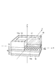
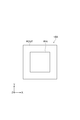
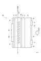
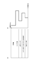
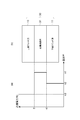
- FIG. 1 is a perspective view showing a configuration of a semiconductor light emitting element 1A as a light emitting device according to a first embodiment of the present invention.
- An XYZ orthogonal coordinate system is defined in which an axis extending through the center of the semiconductor light emitting element 1A and extending in the thickness direction of the semiconductor light emitting element 1A is the Z axis.
- the semiconductor light emitting element 1A is an S-iPM laser that forms a standing wave along an XY plane and outputs a phase-controlled plane wave in the Z-axis direction, and as described later, the main element of the semiconductor substrate 10 A two-dimensional light image of an arbitrary shape is output in the direction perpendicular to the surface 10a (that is, the Z-axis direction) and / or the direction inclined thereto.
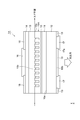
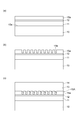
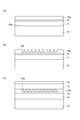
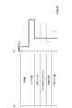
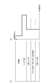
- FIG. 2 is a view schematically showing a laminated structure of the semiconductor light emitting element 1A.
- the semiconductor light emitting element 1A is provided on an active layer 12 as a light emitting portion provided on the main surface 10a of the semiconductor substrate 10 and an active layer 12 provided on the main surface 10a.
- a contact layer 14 provided on the cladding layer 13.
- the semiconductor substrate 10 and the layers 11 to 14 are made of a compound semiconductor such as a GaAs-based semiconductor, an InP-based semiconductor, or a nitride-based semiconductor.
- the energy band gap of the cladding layer 11 and the energy band gap of the cladding layer 13 are larger than the energy band gap of the active layer 12.
- the thickness direction of the semiconductor substrate 10 and the layers 11 to 14 coincides with the Z-axis direction.
- the light guide layer may include a carrier barrier layer for efficiently confining carriers in the active layer 12.
- the semiconductor light emitting device 1A further includes a phase modulation layer 15A optically coupled to the active layer 12.
- the phase modulation layer 15A is provided between the active layer 12 and the cladding layer 13.
- a light guide layer may be provided between the cladding layer 11 and the cladding layer 13 as needed.
- the thickness direction of the phase modulation layer 15A coincides with the Z-axis direction.
- phase modulation layer 15 ⁇ / b> A may be provided between the cladding layer 11 and the active layer 12.
- a light guide layer may be provided between the cladding layer 11 and the cladding layer 13 as needed.
- the phase modulation layer 15A includes a base layer 15a and a plurality of different refractive index areas 15b present in the base layer 15a.
- the base layer 15a is made of a first refractive index medium
- each of the plurality of different refractive index areas 15b is made of a second refractive index medium having a refractive index different from the refractive index of the first refractive index medium.
- the modified refractive index area 15b of the present embodiment is defined by a recess provided in the base layer 15a. In the recess, an inert gas such as argon, nitrogen, hydrogen or air may be enclosed.
- the modified refractive index region 15b may be a hole provided in the base layer 15a.
- the phase modulation layer 15A can select the wavelength ⁇ 0 among the emission wavelengths of the active layer 12 and output it to the outside.
- the light input into the phase modulation layer 15A forms a predetermined mode in the phase modulation layer 15A according to the arrangement of the differential refractive index region 15b, and the back surface of the semiconductor light emitting element 1A is formed as a laser beam having a desired pattern. Output to the outside.
- Each modified refractive index region 15 b has a refractive index interface with the base layer 15 a and a refractive index interface with the cladding layer 13. Then, at least a portion of the refractive index interface between each modified refractive index region 15b and the layer therearound (at least a portion of the surface defining the three-dimensional shape of each modified refractive index region 15b) is the main surface 10a (XY) It is inclined with respect to the plane parallel to the plane) and the normal direction (Z-axis direction) of the major surface 10a.
- each modified refractive index region 15b constitute a refractive index interface with the base layer 15a.
- the upper surface of each modified refractive index region 15 b (the second surface located on the opposite side to the main surface 10 a with respect to the first surface) forms a refractive index interface with the cladding layer 13.
- the bottom surface of each modified refractive index region 15b is perpendicular to the thickness direction of the phase modulation layer 15A (parallel to the XY plane).
- the side surface of each modified refractive index area 15b is along the direction (Z-axis direction) perpendicular to the major surface 10a.
- each modified refractive index region 15b is a direction perpendicular to main surface 10a (parallel to the XY plane) and main surface 10a. It is inclined with respect to (Z-axis direction).
- the inclination directions of the upper surface are aligned with one another in the multiple refractive index regions 15 b.
- Such a shape of the upper surface is realized by a part of the cladding layer 13 getting into the recess of the modified refractive index area 15 b or a part of the modified refractive index area 15 b getting into the cladding layer 13.
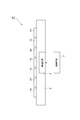
- the semiconductor light emitting element 1A further includes an electrode 16 provided on the contact layer 14 and an electrode 17 provided on the back surface 10b of the semiconductor substrate 10.
- the electrode 16 is in ohmic contact with the contact layer 14, and the electrode 17 is in ohmic contact with the semiconductor substrate 10. Furthermore, the electrode 17 has an opening 17a.
- the electrode 16 is provided in the central region of the contact layer 14. The portion of the contact layer 14 other than the electrode 16 is covered by a protective film 18 (see FIG. 2). The contact layer 14 not in contact with the electrode 16 may be removed. A portion (including the inside of the opening 17 a) of the back surface 10 b of the semiconductor substrate 10 other than the electrode 17 is covered with the anti-reflection film 19. The antireflective film 19 in the area other than the opening 17a may be removed.
- the light output from the active layer 12 enters the inside of the phase modulation layer 15A, and forms a predetermined mode according to the lattice structure formed in the phase modulation layer 15A.
- the laser light output from the phase modulation layer 15A is directly output from the back surface 10b through the opening 17a to the outside of the semiconductor light emitting element 1A or after being reflected by the electrode 16, the opening is made from the back surface 10b.
- the light is output to the outside of the semiconductor light emitting element 1A through 17a. At this time, zero-order light included in the laser light is output in a direction (normal direction) perpendicular to the major surface 10 a.
- signal light (primary light and -1 order light) included in the laser light is output in a two-dimensional arbitrary direction including a direction perpendicular to the major surface 10a and a direction inclined with respect thereto. . It is the signal light that forms the desired light image.
- the semiconductor substrate 10 is a GaAs substrate, and the cladding layer 11, the active layer 12, the cladding layer 13, the contact layer 14, and the phase modulation layer 15A are compound semiconductor layers composed of group III elements and group V elements, respectively.
- the cladding layer 11 is made of AlGaAs.
- the active layer 12 has a multiple quantum well structure (barrier layer: AlGaAs / well layer: InGaAs).
- the basic layer 15a is made of GaAs
- the modified refractive index area 15b is a recess or a hole.
- the cladding layer 13 is made of AlGaAs
- the contact layer 14 is made of GaAs.
- the energy band gap and the refractive index can be easily changed by changing the composition ratio of Al.
- Al x Ga 1 -x As when the composition ratio x of Al having a relatively small atomic radius is decreased (increased), the energy band gap positively correlated with this decreases (large).
- In when In is introduced by mixing In with a large atomic radius into GaAs, the energy band gap decreases. That is, the Al composition ratio of the cladding layers 11 and 13 is larger than the Al composition ratio of the barrier layer (AlGaAs) of the active layer 12.
- the Al composition ratio of the cladding layers 11 and 13 is set to, for example, 0.2 to 1.0 (for example, 0.4).
- the Al composition ratio of the barrier layer of the active layer 12 is set to, for example, 0 to 0.3 (for example, 0.15).
- noise light having a mesh-like dark portion may be superimposed on a beam pattern corresponding to an optical image output from the semiconductor light emitting element 1A.
- the noise light having the mesh-like dark part is caused by the higher order mode in the stacking direction inside the semiconductor light emitting element 1A.
- the fundamental mode in the stacking direction means a mode having an intensity distribution in which one peak exists over the region including the active layer 12 and sandwiched between the cladding layer 11 and the cladding layer 13.
- the higher order mode means a mode having an intensity distribution in which two or more peaks are present.
- the peak of the intensity distribution of the fundamental mode is formed in the vicinity of the active layer 12, while the peak of the intensity distribution of the higher mode is also formed in the cladding layer 11, the cladding layer 13, the contact layer 14 and the like. Further, as modes in the stacking direction, guided modes and leak modes exist, but leak modes do not exist stably. Therefore, in the following description, only the guided mode is focused. Further, in the guided mode, there are TE mode in which the electric field vector exists in the direction along the XY plane, and TM mode in which the electric field vector exists in the direction perpendicular to the XY plane. Focus on the mode only.
- the refractive index of the cladding layer 13 between the active layer 12 and the contact layer is larger than the refractive index of the cladding layer 11 between the active layer 12 and the semiconductor substrate, the higher order mode as described above is remarkable. It occurs.
- the refractive indices of the active layer 12 and the contact layer 14 are much larger than the refractive indices of the cladding layers 11 and 13. Therefore, when the refractive index of the cladding layer 13 is larger than the refractive index of the cladding layer 11, light is confined also in the cladding layer 13 to form a waveguide mode. This results in higher order modes.
- the refractive index of the cladding layer 13 is equal to or less than the refractive index of the cladding layer 11.
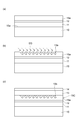
- the optical waveguide layer including the active layer 12 will be described.
- the optical waveguide layer includes only the active layer 12 (the optical waveguide layer includes the cladding layer 11, the cladding layer 13, and the phase modulation layer 15A is not included), it is regarded as a three-layer slab waveguide structure comprising such an optical waveguide layer and upper and lower two layers adjacent to the optical waveguide layer.
- the optical waveguide layer includes the phase modulation layer 15A and the active layer 12 (cladding layer 11 and cladding layer 13 are not included) It is regarded as a three-layer slab waveguide structure including such an optical waveguide layer and two upper and lower layers adjacent to the optical waveguide layer.
- the guided mode in the layer thickness direction is the TE mode.
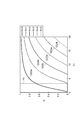
- the normalized propagation constant b of standards influencing for good waveguide width V 1 and TE mode of the optical waveguide layer is defined by the following equation (1).
- the equivalent refractive index of TE mode is a cladding layer so that the waveguide mode does not leak to the semiconductor substrate 10 through the cladding layer 11.
- the refractive index of 11 needs to be higher, and the normalized propagation constant b needs to satisfy the following equation (2).
- a ′ and b each represent an asymmetry parameter and a normalized propagation constant in the three-layer slab waveguide, and are real numbers satisfying the following equations (3) and (4), respectively.
- n clad is the refractive index of the cladding layer 11
- n 1 is the refractive index of the optical waveguide layer including the active layer 12
- n 2 is the layer adjacent to the optical waveguide layer.
- refractive index of the high refractive index layer n 3 is the refractive index of the low layer of the refractive index of the layer adjacent to the optical waveguide layer
- n eff is the two layers of upper and lower adjacent to the optical waveguide layer and the optical waveguide layer It is an equivalent refractive index of TE mode with respect to 3 layer slab waveguide structure.
- the inventors According to the research of the inventors, it has been found that high-order modes are generated also in the optical waveguide layer (high refractive index layer) including the active layer 12. Then, the inventors have found that higher order modes can be suppressed by appropriately controlling the thickness and refractive index of the optical waveguide layer. That is, the value of the standard influencing for good waveguide width V 1 of the optical waveguide layer satisfies the condition described above, generation of higher order modes is further suppressed, and more of the noise light having a net-like dark portion that is superimposed on the beam pattern Further reduction is possible.
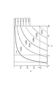
- the preferred thickness of the contact layer 14 is as follows. That is, in the three-layer slab waveguide structure including the contact layer 14 and the two upper and lower layers adjacent to the contact layer 14, the normalized waveguide width V 2 and the normalized propagation constant b of the TE mode are expressed by Defined by). However, when the guided mode is formed in the contact layer (the mode order is N 2 ), the equivalent refractive index of the TE mode is the clad layer 11 so that the guided mode does not leak to the semiconductor substrate 10 through the clad layer 11.
- the normalized propagation constant b needs to satisfy the following equation (6). At this time, as long as it is within the range of No that the equation (5) and (6) Standard influencing for good waveguide width V 2 collapsed meet, mode guided through the contact layer 14 is even not exist fundamental mode.
- a ′ and b respectively represent an asymmetry parameter and a normalized propagation constant in the three-layer slab waveguide, and are real numbers satisfying the following equations (7) and (8), respectively.
- n 4 is the refractive index of the contact layer 14
- n 5 is the refractive index of the layer having a high refractive index among the layers adjacent to the contact layer 14
- n 6 is the contact layer Among the layers adjacent to S.14 , the refractive index of the layer having a low refractive index among the adjacent layers
- n eff is the equivalent refractive index of the TE mode with respect to the contact layer 14 and the adjacent three-layer slab waveguide structure of upper and lower two layers.
- the generation of the guided mode caused by the contact layer 14 can be suppressed, and the generation of the higher order mode generated in the semiconductor light emitting device can be further suppressed.
- the semiconductor substrate 10 is an InP substrate, and the cladding layer 11, the active layer 12, the phase modulation layer 15A, the cladding layer 13, and the contact layer 14 are made of, for example, an InP-based compound semiconductor.
- the cladding layer 11 is made of InP.
- the active layer 12 has a multiple quantum well structure (barrier layer: GaInAsP / well layer: GaInAsP).
- the basic layer 15a is made of GaInAsP
- the modified refractive index area 15b is a recess (may be a void).
- the cladding layer 13 is made of InP.
- the contact layer 14 is made of GaInAsP.
- the semiconductor substrate 10 is a GaN substrate
- the cladding layer 11, the active layer 12, the phase modulation layer 15A, the cladding layer 13, and the contact layer 14 are made of, for example, a nitride compound semiconductor.
- the cladding layer 11 is made of AlGaN.
- the active layer 12 has a multiple quantum well structure (barrier layer: InGaN / well layer: InGaN).
- the basic layer 15a is made of GaN
- the modified refractive index area 15b is a recess (may be a void).
- the cladding layer 13 is made of AlGaN.
- the contact layer 14 is made of GaN.
- the same conductivity type as the semiconductor substrate 10 is given to the cladding layer 11, and the opposite conductivity type to the semiconductor substrate 10 is given to the cladding layer 13 and the contact layer 14.
- the semiconductor substrate 10 and the cladding layer 11 are n-type, and the cladding layer 13 and the contact layer 14 are p-type.
- the phase modulation layer 15A has the same conductivity type as the semiconductor substrate 10.
- the phase modulation layer 15A is provided between the active layer 12 and the cladding layer 13, the phase modulation layer 15A has a conductivity type opposite to that of the semiconductor substrate 10.
- the impurity concentration is, for example, 1 ⁇ 10 17 to 1 ⁇ 10 21 / cm 3 .
- the active layer 12 is intrinsic (i-type) to which no impurity is intentionally added, and the impurity concentration is 1 ⁇ 10 15 / cm 3 or less. Further, the impurity concentration of the phase modulation layer 15A may be intrinsic (i-type), for example, when it is necessary to suppress the influence of loss due to light absorption through the impurity level.
- the thickness of the semiconductor substrate 10 is, for example, 150 ⁇ m.
- the thickness of the cladding layer 11 is, for example, 2000 nm.
- the thickness of the active layer 12 is, for example, 175 nm.
- the thickness of the phase modulation layer 15A is, for example, 280 nm.
- the depth of the modified refractive index area 15b is, for example, 200 nm.
- the thickness of the cladding layer 13 is, for example, 2000 nm.
- the thickness of the contact layer 14 is, for example, 150 nm.
- the antireflective film 19 is made of, for example, a dielectric single layer film such as silicon nitride (for example, SiN), silicon oxide (for example, SiO 2 ) or the like, or a dielectric multilayer film.
- dielectric multilayer films include titanium oxide (TiO 2 ), silicon dioxide (SiO 2 ), silicon monoxide (SiO), niobium oxide (Nb 2 O 5 ), tantalum pentoxide (Ta 2 O 5 ), and fluorine.
- Dielectric layers such as magnesium fluoride (MgF 2 ), titanium oxide (TiO 2 ), aluminum oxide (Al 2 O 3 ), cerium oxide (CeO 2 ), indium oxide (In 2 O 3 ), zirconium oxide (ZrO 2 )
- MgF 2 magnesium fluoride
- TiO 2 titanium oxide
- Al 2 O 3 aluminum oxide
- CeO 2 cerium oxide
- In 2 O 3 indium oxide
- a film in which two or more types of dielectric layers selected from the group are stacked can be used.
- a film with a thickness of ⁇ / 4 is stacked with an optical film thickness for light of wavelength ⁇ .
- the protective film 18 is, for example, an insulating film such as silicon nitride (for example, SiN) or silicon oxide (for example, SiO 2 ).
- the electrode 16 can be made of a material containing at least one of Cr, Ti, and Pt, and Au, for example, a Cr layer and an Au layer.
- the electrode 17 can be made of a material containing at least one of AuGe and Ni, and Au, and has, for example, a laminated structure of an AuGe layer and an Au layer.
- the materials of the electrodes 16 and 17 are not limited to these ranges as long as ohmic contact can be realized.
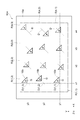
- FIG. 4 is a plan view of the phase modulation layer 15A.
- the phase modulation layer 15A includes the base layer 15a and the modified refractive index area 15b.
- the base layer 15a is made of a first refractive index medium
- the modified refractive index area 15b is made of a second refractive index medium having a refractive index different from that of the first refractive index medium.
- a virtual square lattice is set on the design surface of the phase modulation layer 15A that coincides with the XY plane. One side of the square lattice is parallel to the X axis, and the other side is parallel to the Y axis.
- a square unit configuration region R centered on the lattice point O of the square lattice can be set in a two-dimensional manner over a plurality of columns along the X axis and a plurality of rows along the Y axis.
- a square unit configuration region R centered on the lattice point O of the square lattice is arranged in parallel along a plurality of columns (x1 to x4) arranged in parallel along the X axis and the Y axis.
- a plurality of lines (y1 to y3) are set in a two-dimensional manner.
- the modified refractive index areas 15 b are provided one by one in each unit configuration area R.
- the lattice point O may be located outside the modified refractive index area 15 b or may be included inside the modified refractive index area 15 b.
- the planar shape of each of the plurality of modified refractive index regions 15b is a shape in which the width in a certain direction on the XY plane gradually narrows along the direction intersecting the direction.
- FIG. 4 shows a triangular shape as an example of such a shape. That is, it has a shape in which the width gradually narrows from a certain side toward the vertex facing the side. This triangle is, for example, an isosceles triangle. As shown in FIGS.
- the refractive index interface defined by the modified refractive index region 15 b and at least one of the cladding layer 11 and the active layer 12 has a principal surface 10 a (X ⁇ It is inclined with respect to a direction (Z-axis direction) perpendicular to the Y plane) and the major surface 10a.
- the inclination direction coincides with the direction from a certain side to the vertex opposite to the side.
- the directions are aligned with one another in the plurality of different refractive index regions 15b. In one example, the angle between this direction and the X-axis direction is 45 ° or 135 °.
- the ratio of the area SA of the differential refractive index area 15b occupied in one unit constituent area R is referred to as a filling factor (FF).
- FF filling factor
- SA is the area of the modified refractive index area 15b in the XY plane.
- LA LA ⁇ h / 2.
- the lattice spacing a of the square lattice is about the wavelength divided by the equivalent refractive index, and is set to, for example, about 300 nm.
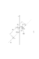
- FIG. 5 is a view showing the positional relationship of the modified refractive index area 15b in the phase modulation layer 15A.
- the center of gravity G of each modified refractive index area 15 b is disposed on the straight line D.
- the straight line D is a straight line that passes through the corresponding grid point O (x, y) of the unit constituent region R (x, y) and is inclined with respect to each side of the square lattice.
- the straight line D is a straight line inclined with respect to both the s axis (parallel to the X axis) and the t axis (parallel to the Y axis) defining the unit constituent region R (x, y).
- the inclination angle of the straight line D with respect to the s axis (inclination angle based on a part of the s axis starting from the lattice point) is ⁇ .
- the inclination angle ⁇ is constant in the phase modulation layer 15A (a part of the phase modulation layer 15A may be constant).
- the straight line D extends from the first quadrant to the third quadrant of the coordinate plane defined by the s-axis and t-axis. .
- the straight line D extends from the second quadrant to the fourth quadrant of the coordinate plane defined by the s-axis and t-axis. .
- the inclination angle ⁇ is an angle excluding 0 °, 90 °, 180 ° and 270 °.
- the distance between the grid point O (x, y) and the center of gravity G is r (x, y).
- x indicates the position of the x-th grid point on the X axis
- y indicates the position of the y-th grid point on the Y axis.
- the center of gravity G is located in the first quadrant (or the second quadrant).
- the distance r (x, y) is a negative value
- the center of gravity G is located in the third quadrant (or the fourth quadrant).
- the distance r (x, y) is zero, the grid point O and the center of gravity G coincide with each other.
- the different refractive index areas 15b are individually set according to the beam pattern (light image). That is, the distribution of the distance r (x, y) has a specific value at each position determined by the values of x (x1 to x4 in the example of FIG. 4) and y (y1 to y3 in the example of FIG. 4). It is not necessarily represented by a specific function.
- the distribution of the distance r (x, y) is determined from the complex amplitude distribution obtained by inverse Fourier transform of the output beam pattern from which the phase distribution is extracted. That is, when the phase P (x, y) in the unit constituent region R (x, y) is P 0 described later, the distance r (x, y) is set to 0, and the phase P (x, y) distance r (x, y) is set to the maximum value R 0 is when There is a ⁇ + P 0, when the phase P (x, y) is a - [pi] + P 0 is distance r (x, y) is the minimum value -R Set to 0 .
- the initial phase P 0 can be set arbitrarily.
- the maximum value R 0 of r (x, y) is, for example, within the range of the following formula (9). Note that when finding the complex amplitude distribution from the output beam pattern, the reproducibility of the beam pattern is improved by applying an iterative algorithm such as the Gerchberg-Saxton (GS) method that is generally used when calculating the hologram generation. Do.
- FIG. 6 is a plan view showing an example in which the substantially periodic refractive index structure of FIG. 4 is applied only in a specific region of the phase modulation layer.
- a substantially periodic structure for outputting a desired beam pattern is formed inside the square inner region RIN.
- the outer region ROUT surrounding the inner region RIN a circular different refractive index region having a coincident barycentric position is disposed at the grid point position of the square lattice.
- light is also distributed in the outer region ROUT to suppress generation of high frequency noise (so-called window function noise) caused by a sudden change in light intensity in the peripheral portion of the inner region RIN. it can.
- window function noise high frequency noise
- light leakage in a direction parallel to the XY plane can be suppressed, and reduction in threshold current can be expected.
- FIG. 7 is a diagram for explaining the relationship between the output beam pattern (optical image) from the semiconductor light emitting element 1A and the distribution of distances in the phase modulation layer 15A.
- a Kx-Ky plane obtained by converting a beam projection area, which is a projection area of an output beam pattern, onto a wave number space.
- the Kx-axis and the Ky-axis defining the Kx-Ky plane are orthogonal to each other, and each projects the projection direction of the output beam pattern from the normal direction (Z-axis direction) of the main surface 10a to the in-plane of the main surface 10a. It corresponds to an angle with respect to the normal direction when it is shaken in the direction (details will be described later).
- a specific region including an output beam pattern is constituted by M2 (an integer of 1 or more) ⁇ N2 (an integer of 1 or more) square image regions FR.
- a virtual square lattice set on the design surface (X-Y plane) of the phase modulation layer 15A is configured by M1 (an integer of 1 or more) ⁇ N1 (an integer of 1 or more) unit configuration regions R Shall be
- M2 does not have to match the integer M1.
- the integer N2 does not have to match the integer N1.
- the image region FR (k x , k y ) in each is specified by the coordinate component x (an integer of 1 or more and M1 or less) in the X axis direction and the coordinate component y (an integer of 1 or more and N1 or less) in the Y axis direction
- the complex amplitude F (x, y) in the unit constituent region R (x, y) subjected to the two-dimensional inverse Fourier transform to the unit constituent region R (x, y) is the amplitude term A (x, y) and the phase term P (P It is defined by x, y).
- the amplitude term A in the complex amplitude F (x, y) of the unit constituent region R (x, y) corresponds to the amplitude distribution on the XY plane.
- the distribution of the phase term P (x, y) in the complex amplitude F (x, y) of the unit constituent region R (x, y) is X ⁇ It corresponds to the phase distribution on the Y plane.
- the distribution of the distance r (x, y) of (x, y) corresponds to the distance distribution on the XY plane.
- FIG. 7 shows four quadrants whose origin is the center Q. .
- FIG. 7 shows the case where light images are obtained in the first and third quadrants as an example, it is also possible to obtain images in the second and fourth quadrants or all quadrants.
- a pattern symmetrical with respect to the origin is obtained.
- FIG. 7 shows, as an example, a case where a pattern obtained by rotating the letter "A" in the third quadrant and the letter "A" in the first quadrant by 180 ° is obtained.
- a rotationally symmetric light image for example, a cross, a circle, a double circle, etc.
- the light images are superimposed and observed as one light image.
- the output beam pattern (optical image) of the semiconductor light emitting element 1A is at least one of a spot, a spot group consisting of three or more points, a straight line, a cross, a line drawing, a lattice pattern, a photograph, a stripe pattern, CG (computer graphics) and characters.
- the light image corresponds to the designed light image (original image) represented by one.
- the distribution of the distance r (x, y) of the modified refractive index area 15b of the phase modulation layer 15A is determined by the following procedure.
- FIG. 8 is a diagram for explaining coordinate conversion from spherical coordinates (d1, ⁇ tilt , ⁇ rot ) to coordinates ( ⁇ , ⁇ , ⁇ ) in the XYZ orthogonal coordinate system, and the coordinates ( ⁇ , ,, By ⁇ ), a designed light image on a predetermined plane set in the XYZ rectangular coordinate system which is a real space is expressed.
- the angle theta tilt and theta rot has the following formula (13)
- the coordinate value k x on the Kx axis corresponding to the X axis, and the normalized wave number defined by the following equation (14) corresponding to the Y axis and along the Kx axis shall be converted into coordinate values k y on Ky axis orthogonal.
- the normalized wave number means the wave number normalized with the wave number corresponding to the lattice spacing of a virtual square lattice being 1.0.
- a specific wave number range including a beam pattern corresponding to an optical image is square M2 (integer of 1 or more) .times.N2 (integer of 1 or more) And the image region FR.
- the integer M2 does not have to match the integer M1.
- the integer N2 does not have to match the integer N1.
- Formula (13) and Formula (14) are described in the following document (1), for example.
- the corresponding different refractive index regions 15 b are disposed in the unit constituent region R (x, y) so as to satisfy the following relationship.
- the distance r (x, y) is set to 0 when the phase P (x, y) at a certain coordinate (x, y) is P 0 , and the phase P (x, y) is ⁇ + P 0
- the maximum value R 0 is set
- the minimum value ⁇ R 0 is set.
- the light image is subjected to inverse Fourier transform, and the distribution of the distance r (x, y) according to the phase P (x, y) of its complex amplitude is divided into a plurality of different refractive index regions Give it to 15b.
- the phase P (x, y) and the distance r (x, y) may be proportional to one another.
- the far-field pattern after Fourier transform of the laser beam has various shapes such as single or plural spot shapes, annular shapes, linear shapes, character shapes, double annular shapes, or Laguerre-Gaussian beam shapes. It can be taken. Since the beam direction can also be controlled, it is possible to realize, for example, a laser processing machine that electrically performs high-speed scanning by arraying the semiconductor light emitting elements 1A in one or two dimensions. Since the beam pattern is represented by angle information in the far field, if the target beam pattern is a bitmap image or the like represented by two-dimensional position information, it is once converted into angle information. Then, it is preferable to perform inverse Fourier transform after converting to wave number space.
- the amplitude distribution A (x, y) is calculated by using the abs function of the numerical analysis software "MATLAB" of The MathWorks.
- the phase distribution P (x, y) can be calculated by using MATLAB's angle function.
- FIG. 9B An output beam pattern calculated from the complex amplitude distribution obtained by the inverse Fourier transform of FIG. 9A, which is a desired light image, is as shown in FIG. 9B.
- the first quadrant of the output beam pattern shown in FIG. 9B is divided into four quadrants A1, A2, A3, and A4.
- the first quadrant of the original optical image is in the third quadrant of the obtained beam pattern.
- a pattern obtained by rotating the first quadrant of the original light image by 180 degrees appears in the first quadrant of the obtained beam pattern.
- the material system, the film thickness, and the layer structure may be variously changed.
- a scaling law holds. That is, when the wavelength is multiplied by a constant ⁇ , a similar standing wave state can be obtained by multiplying the entire square lattice structure by ⁇ .
- each compound semiconductor layer is formed by metal organic chemical vapor deposition (MOCVD) or molecular beam epitaxy (MBE).
- MOCVD metal organic chemical vapor deposition
- MBE molecular beam epitaxy
- the growth temperature of AlGaAs can be set to 500 ° C. to 850 ° C.
- TMA trimethylaluminum
- TMG trimethylgallium
- TEG triethylgallium
- AsH 3 arsine
- Si 2 H 6 source material for N-type impurities DEZn (diethyl zinc) is used as a raw material for disilane
- P-type impurities is used as a raw material for disilane.
- In the growth of GaAs TMG and arsine are used, but TMA is not used.
- InGaAs is manufactured using TMG, TMI (trimethylindium) and arsine.
- the insulating film is formed by sputtering a target using the constituent material as a raw material or by PCVD (plasma CVD).
- FIG. 10A are diagrams showing steps in the method of manufacturing the semiconductor light emitting device 1A.
- the cladding layer 11, the active layer 12, and the base layer 15a are formed on the major surface 10a of the semiconductor substrate 10 by, for example, MOCVD (metal organic chemical vapor deposition) method. It is sequentially provided by the used epitaxial growth method.
- MOCVD metal organic chemical vapor deposition
- a two-dimensional fine pattern is drawn on the resist by an electron beam drawing apparatus.
- a two-dimensional fine pattern is formed on the resist by developing the resist on which the pattern is drawn.
- the two-dimensional fine pattern is transferred to the basic layer 15a by dry etching.
- a plurality of recesses may be formed to become the modified refractive index regions 15b.
- the planar shape of the plurality of recesses is, as described above, a shape in which the width in a certain direction gradually narrows along the direction crossing the direction (for example, a triangular shape, see FIG. 4).
- a step of forming a SiN layer or SiO 2 layer on the base layer 15a by PCVD before forming the resist a step of forming a resist mask on the formed layers (SiN layer or SiO 2 layer)
- the step of transferring the fine pattern to the SiN layer or the SiO 2 layer by reactive ion etching (RIE), and the step of performing dry etching after removing the resist may be sequentially performed. In this case, the resistance of dry etching can be enhanced.
- the cladding layer 13 and the contact layer 14 are sequentially provided by the MOCVD method.
- the cladding layer 13 is grown, the plurality of recesses as the modified refractive index regions 15 b are closed by the cladding layer 13.
- the degree of the entry changes in the recess due to the planar shape of the recess. That is, the degree of penetration of the cladding layer 13 changes between the wide portion of the recess and the narrow portion of the recess.
- the refractive index interface between the cladding layer 13 and the modified refractive index region 15 b is inclined with respect to the interface between the base layer 15 a and the cladding layer 13. Since the interface between the basic layer 15a and the cladding layer 13 is parallel to the major surface 10a, the refractive index interface between the cladding layer 13 and the modified refractive index region 15b is in the direction perpendicular to the major surface 10a and the major surface 10a. Will be inclined.
- FIG. 10C shows an example in which a part of the cladding layer 13 enters the recess, the recess may enter the cladding layer 13 in reverse. Such a method is described in the following document (2).
- Kazuyoshi Hirose et al. “Watt-class high-power, high-beam-quality photonic-crystal lasers”, Nature Phoronics 8, pp. 406-411 (2014)
- the electrodes 16 and 17 shown in FIG. 2 are formed by vapor deposition, sputtering or the like.
- the protective film 18 and the antireflective film 19 are formed by a sputtering method, a PCVD method, or the like, as necessary.
- the semiconductor light emitting element 1A of the present embodiment is manufactured through the above steps.
- the phase modulation layer 15A is provided between the active layer 12 and the cladding layer 11, the phase modulation layer 15A is formed on the cladding layer 11 before the formation of the active layer 12.
- the wave number k exists at the saddle point, but the size of the wave number vector is basically inverse If it is equal to the magnitude of the grating vector, a resonant mode (a standing wave in the XY plane) with a grating spacing a equal to the wavelength ⁇ is obtained. In the present embodiment, oscillation in such a resonance mode (standing wave state) is obtained.
- the standing wave in the phase modulation layer 15A described above is scattered by the different refractive index area 15b having a predetermined shape, and the wavefront obtained in the vertical direction (Z-axis direction) is phase-modulated.
- the desired beam pattern is obtained. For this reason, a desired beam pattern can be obtained without the polarizing plate.
- This beam pattern is not only a pair of single-peak beams (spots), but also, as described above, a character shape, two or more identical shape spot groups, or a vector whose phase and intensity distribution are spatially nonuniform. It is also possible to use a beam or the like.
- the refractive index of the basic layer 15a is preferably 3.0 to 3.5, and the refractive index of the modified refractive index region 15b is preferably 1.0 to 3.4.
- the average radius of the recess (different refractive index region 15b) of the basic layer 15a is, for example, 20 nm to 120 nm in the case of the 940 nm band.
- the diffraction efficiency is proportional to the light coupling coefficient ⁇ 1 represented by a first-order coefficient when Fourier transforming the shape of the modified refractive index area 15b.
- the light coupling coefficient is described, for example, in the following document (3).
- the phase modulation layer 15A optically coupled to the active layer 12 includes the base layer 15a and a plurality of different refractive index regions 15b having refractive indexes different from the refractive index of the base layer 15a. And.
- the lattice point O (x, y) including the lattice point O (x, y) of the virtual square lattice set on the design surface of the phase modulation layer 15A, the lattice point O (x, y) And a straight line D inclined with respect to each side of the square lattice (parallel to the s-axis and the t-axis defining the unit constituent region R (x, y)).
- the center of gravity G is arranged.
- the distance r (x, y) between the center of gravity G of the modified refractive index area 15 b and the corresponding lattice point O (x, y) is individually set for each lattice point according to the light image.
- the phase of the beam changes according to the distance between the lattice point O (x, y) and the center of gravity G. Therefore, only by changing the position of the center of gravity G, the phase of the beam output from each of the different refractive index areas 15b can be controlled, and the beam pattern formed as a whole can be controlled to a desired shape. Become.
- this semiconductor light emitting element 1A is an S-iPM laser, and according to such a structure, the center of gravity G of each modified refractive index area 15b is rotated according to the light image around each lattice point O (x, y) As in the conventional structure (rotation method) having an angle, the light forming an optical image of an arbitrary shape is output in the direction inclined with respect to the direction (normal direction) perpendicular to the major surface 10 a of the semiconductor substrate 10 be able to.
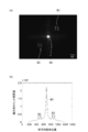
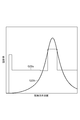
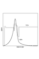
- FIG. 11A shows an example of a beam pattern (optical image) output from the semiconductor light emitting element 1A.
- the center of FIG. 11A corresponds to an axis that intersects the light emitting surface of the semiconductor light emitting element 1A and is perpendicular to the light emitting surface.
- FIG. 11B is a graph showing the light intensity distribution in a cross section including the axis. Fig.
- FIG. 11 (b) is a far-field image acquired using an FFP optical system (A3267-12 manufactured by Hamamatsu Photonics), a camera (ORCA-05G manufactured by Hamamatsu Photonics), and a beam profiler (Lepas-12 manufactured by Hamamatsu Photonics) It is the image which integrated
- the maximum count number in FIG. 11A is normalized at 255, and the central zero-order light B0 is saturated in order to clearly show the intensity ratio of ⁇ first-order light. From FIG. 11 (b), the difference in intensity between the primary light and the ⁇ 1st light can be easily understood.
- FIG. 11 (b) is a far-field image acquired using an FFP optical system (A3267-12 manufactured by Hamamatsu Photonics), a camera (ORCA-05G manufactured by Hamamatsu Photonics), and a beam profiler (Lepas-12 manufactured by Hamamatsu Photonics) It is the
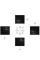
- FIGS. 12 (a) is a diagram showing a phase distribution corresponding to the beam pattern shown in FIG. 11 (a).
- FIG.12 (b) is the elements on larger scale of Fig.12 (a).
- the phase at each position in the phase modulation layer 15A is indicated by shading, and the darker part approaches the phase angle 0 °, and the bright part approaches the phase angle 360 °.
- the center value of the phase angle can be set arbitrarily, the phase angle may not necessarily be set within the range of 0 ° to 360 °.
- the semiconductor light emitting device 1A includes a primary light including a first light image portion B1 outputted in a first direction inclined with respect to the axis.
- the first light is output in a second direction that is symmetrical to the first direction with respect to the axis, and the first order light including the second light image portion B2 that is rotationally symmetrical with the first light image portion B1 with respect to the axis.
- the first light image portion B1 appears in the first quadrant in the XY plane
- the second light image portion B2 appears in the third quadrant in the XY plane.
- either primary light or negative primary light may not be required. In such a case, it is desirable to reduce unnecessary light of the primary light and the ⁇ 1st light with respect to the necessary light.
- FIG. 13 is a diagram conceptually showing an example of beam patterns of traveling waves in each direction.
- the inclination angle of the straight line D with respect to the s-axis and the t-axis is 45 °
- the maximum value R 0 of the distance r (x, y) to y) is set as in the following equation (17).
- fundamental traveling waves AU, AD, AR and AL are generated along the XY plane.
- the traveling waves AU and AD are lights traveling along one of the sides of the square lattice extending in the Y-axis direction.
- the traveling wave AU travels in the positive Y-axis direction
- the traveling wave AD travels in the negative Y-axis direction.
- the traveling waves AR and AL are light traveling along a side of the sides of the square lattice extending in the X-axis direction.
- the traveling wave AR travels in the positive X-axis direction
- the traveling wave AL travels in the negative X-axis direction. In this case, from the traveling waves traveling in opposite directions to each other, beam patterns in opposite directions can be obtained.
- a beam pattern BU including only the second light image portion B2 is obtained from the traveling wave AU, and a beam pattern BD including only the first light image portion B1 is obtained from the traveling wave AD.
- a beam pattern BR including only the second light image portion B2 is obtained from the traveling wave AR, and a beam pattern BL including only the first light image portion B1 is obtained from the traveling wave AL.
- one is primary light and the other is negative first-order light.
- phase modulation layer 15A of the present embodiment for a single traveling wave, a difference occurs in the light amount of each of the first-order light and the -1st-order light.
- the ideal phase distribution is obtained as the shift amount R 0 approaches the upper limit value of the above equation (9).
- the 0th-order light is reduced, and in each of the traveling waves AU, AD, AR, and AL, one of the 1st-order light and the -1st-order light is selectively reduced. Therefore, it is possible in principle to give a difference to the light amounts of the primary light and the ⁇ 1st light by selectively reducing any one of the traveling waves traveling in opposite directions.
- the method of the present embodiment in which the modified refractive index area 15b moves on the straight line D which passes through the lattice point O (x, y) and is inclined with respect to each side of the square lattice shown in FIG. The reason why it is possible to selectively reduce either the primary light or the ⁇ 1st light will be described.
- the design phase ⁇ (x, y) at a certain position the t axis (parallel to the Y axis) positive shown in FIGS. 12 (a) and 12 (b) as an example of four traveling waves.
- the traveling wave AU in the direction.
- the shift from the lattice point O is r ⁇ sin ⁇ ⁇ ⁇ (x, y) ⁇ 0 ⁇ / ⁇ , so the phase difference is The relation is 2 ⁇ / a) r ⁇ sin ⁇ ⁇ ⁇ (x, y) ⁇ 0 ⁇ / ⁇ .
- a function f (z) represented by the following equation (19) and satisfying the following equation (20) is expanded by Laurent series, a mathematical formula such as the following equation (21) holds.
- sinc (x) x / sin (x).
- the phase distribution ((x, y) can be subjected to series expansion, and the respective light quantities of the zeroth order light and the ⁇ first order lights can be described.
- the magnitude of the zero-order light component of the phase distribution ((x, y) is as follows, when it is noted that the absolute value of the exponent term exp ⁇ j ⁇ (c ⁇ n) ⁇ in the above equation (21) is 1.
- the magnitude of the primary light component is represented by the following formula (23)
- the magnitude of the ⁇ 1st order light component is represented by the following formula (24).
- zero-order light and minus first-order light components appear in addition to the first-order light component except under the condition defined by the following formula (25).
- the magnitudes of the ⁇ 1st-order light components are not equal to one another.
- the traveling wave AU in the t-axis direction (Y-axis positive direction) is considered as an example of the four traveling waves, but the same relationship applies to the other three waves (traveling waves AD, AR, AL) This holds true, and a difference occurs in the magnitude of ⁇ 1st-order light components.
- the interface between the modified refractive index region 15b and the upper layer (cladding layer 13 or active layer 12) is inclined with respect to the major surface 10a.
- the traveling waves AU, AD, AR, and AL traveling in the phase modulation layer 15A in parallel with the major surface 10a are phased at the interface between the differential refractive index region 15b and the upper layer thereof.
- the light is scattered or reflected in a direction (for example, the Z-axis direction) intersecting the design surface (the plane parallel to the XY plane) of the modulation layer 15A.
- two traveling waves AU and AD traveling in opposite directions along the major surface 10a in the phase modulation layer 15A are scattered or reflected in mutually different directions, and are separated from each other.
- two traveling waves AR and AL traveling in opposite directions in the plane of the phase modulation layer 15A are scattered or reflected in different directions, and are separated from each other.
- the traveling waves AU and AR which are primary light (or ⁇ 1st light) are scattered or reflected toward the semiconductor substrate 10, and the traveling waves AD and AL which are ⁇ 1st light (or 1st light) are semiconductors
- the light is scattered or reflected toward the side (electrode 16 side) opposite to the substrate 10. Therefore, the optical paths until the light is output to the outside of the device are different between the primary light and the ⁇ 1st light. Since the traveling waves AU and AR are scattered or reflected toward the semiconductor substrate 10, they pass through the semiconductor substrate 10 and are output to the outside as they are, and the optical path becomes short.
- the traveling waves AD and AL are scattered or reflected toward the opposite side to the semiconductor substrate 10, they are reflected by the electrode 16 and reach the semiconductor substrate 10 by an amount equal to that of the traveling waves AU and AR. Will be longer. Therefore, the traveling waves AD and AL are attenuated more than the traveling waves AU and AR due to the effects of light absorption in the semiconductor, incomplete reflection at the electrode 16, and scattering accompanying light propagation. Therefore, according to the semiconductor light emitting device 1A of the present embodiment, it is possible to reduce one of the primary light and the ⁇ 1st light with respect to the other light. Also in FIG. 11 (b) corresponding to the experimental result, it can be seen that there is a difference in intensity between the primary light and the ⁇ 1st light.
- the interface between the modified refractive index region 15b and the upper layer thereof is inclined with respect to the major surface 10a, but this is an example.
- the above-described effect can be suitably obtained by at least a part of the interface between the plurality of different refractive index areas 15b and the layer therearound being inclined with respect to the major surface 10a.
- the light emitting device including the semiconductor light emitting device 1A or the semiconductor light emitting device 1A attenuates one light.
- the light emitting device including the semiconductor light emitting device 1A or the semiconductor light emitting device 1A attenuates one light.
- a light absorbing layer provided between the phase modulation layer 15A and the semiconductor substrate 10 a light absorbing member provided outside the semiconductor light emitting element 1A, etc.
- one light may be output from the surface on the opposite side to the other light (that is, the surface on the side of the cladding layer 13 with respect to the active layer 12).
- the plurality of modified refractive index regions 15b are concave portions, and the planar shape of each of the plurality of modified refractive index regions 15b is gradually along the direction in which the width in one direction intersects the direction It may be narrow in shape.
- the interface between the semiconductor layer and the different refractive index region 15b is inclined with respect to the major surface 10a. Therefore, a configuration in which at least a part of the interface between the plurality of different refractive index regions 15 b and the layer therearound is inclined with respect to the major surface 10 a can be easily realized.
- the inclination angle ⁇ of the straight line D with respect to the square lattice may coincide at all lattice points set in the phase modulation layer 15A. This makes it possible to easily design the arrangement of the center of gravity G of the modified refractive index area 15b. Also, in this case, the inclination angle ⁇ may be 45 °, 135 °, 225 ° or 315 °. Thereby, two waves (for example, traveling waves AD, AR) orthogonal to each other traveling along the square lattice can equally contribute to the formation of a desired light image.
- traveling waves AD, AR orthogonal to each other traveling along the square lattice
- the inclination angle ⁇ is 0 °, 90 °, 180 ° or 270 °
- a pair of the progressions in the Y-axis direction or the X-axis direction out of the four traveling waves AU, AD, AR, and AL Since the wave does not contribute to the primary light (signal light), it is difficult to improve the efficiency of the signal light.
- the light emitting unit may be the active layer 12 provided on the semiconductor substrate 10. Thereby, the light emitting portion and the phase modulation layer 15A can be easily optically coupled.
- FIG. 15 is a view showing a cross-sectional structure of a semiconductor light emitting element 1B as a light emitting device according to the second embodiment.
- the semiconductor light emitting element 1B is a laser light source that forms a standing wave along the XY plane and outputs a phase controlled plane wave in the Z axis direction, and as in the first embodiment, the semiconductor substrate 10
- the light which forms a two-dimensional light image of an arbitrary shape is output in a direction including a direction (normal direction) perpendicular to the major surface 10a and an inclined direction inclined with respect to the normal direction.
- the semiconductor light emitting element 1A of the first embodiment outputs the beam pattern (optical image) transmitted through the semiconductor substrate 10 from the back surface
- the semiconductor light emitting element 1B of this embodiment has the cladding layer 13 with respect to the active layer 12.
- the beam pattern (light image) is output from the side surface.
- the semiconductor light emitting device 1B includes a cladding layer 11, an active layer 12, a cladding layer 13, a contact layer 14, a phase modulation layer 15A, and a current confinement layer 21.
- the cladding layer 11 is provided on the semiconductor substrate 10.
- the active layer 12 is provided on the cladding layer 11.
- the cladding layer 13 is provided on the active layer 12.
- the contact layer 14 is provided on the cladding layer 13.
- the phase modulation layer 15 A is provided between the active layer 12 and the cladding layer 13.
- the current confinement layer 21 is provided in the cladding layer 13.
- the configuration (preferred material, band gap, refractive index, etc.) of each of the layers 11 to 14 and 15 A is the same as that of the first embodiment.
- phase modulation layer 15A The structure of the phase modulation layer 15A is the same as that of the phase modulation layer 15A (see FIGS. 4 and 5) described in the first embodiment.
- a light guide layer may be provided between the cladding layer 11 and the cladding layer 13 as needed.
- a phase modulation layer 15A may be provided between the cladding layer 11 and the active layer 12.
- the light guide layer may include a carrier barrier layer for efficiently confining carriers in the active layer 12.
- the semiconductor light emitting element 1 B further includes an electrode 23 provided on the contact layer 14 and an electrode 22 provided on the back surface 10 b of the semiconductor substrate 10.
- the electrode 23 is in ohmic contact with the contact layer 14, and the electrode 22 is in ohmic contact with the semiconductor substrate 10.
- FIG. 17 is a plan view of the semiconductor light emitting element 1B as viewed from the electrode 23 side (surface side). As shown in FIG. 17, the electrode 23 has a frame-like (annular) planar shape (having an opening 23a).
- the square frame-shaped electrode 23 is illustrated by FIG. 17, various shapes, such as annular
- the 17 is similar to the shape of the opening 23a of the electrode 23, and is, for example, square or circular.
- the inner diameter of the opening 23a of the electrode 23 (length of one side when the shape of the opening 23a is a square) is, for example, 20 ⁇ m to 50 ⁇ m.
- the contact layer 14 of the present embodiment has a planar shape similar to that of the electrode 23. That is, the central portion of the contact layer 14 is removed by etching to form an opening 14 a.
- the contact layer 14 has a frame-like (annular) planar shape.
- the light output from the semiconductor light emitting element 1 B passes through the opening 14 a of the contact layer 14 and the opening 23 a of the electrode 23.
- the contact layer 14 may cover the entire surface of the cladding layer 13 without the opening 14 a.
- light can be suitably output from the surface side of the semiconductor light emitting element 1 B without being blocked by the electrode 23.
- the surface of the cladding layer 13 exposed from the opening 14 a of the contact layer 14 (or the surface of the contact layer 14 when the opening 14 a is not provided) is covered with the anti-reflection film 25.
- An antireflective film 25 may be provided on the outside of the contact layer 14. Further, a portion other than the electrode 22 on the back surface 10 b of the semiconductor substrate 10 is covered with a protective film 24.
- the material of the protective film 24 is the same as that of the protective film 18 of the first embodiment.
- the material of the antireflective film 25 is the same as that of the antireflective film 19 of the first embodiment.
- the current confinement layer 21 has a structure in which current does not easily pass (or does not pass), and has an opening 21 a in the center. As shown in FIG. 17, the planar shape of the opening 21a is similar to the shape of the opening 23a of the electrode 23, and is, for example, square or circular.
- the current confinement layer 21 is, for example, an Al oxide layer formed by oxidizing a layer containing Al at a high concentration.
- the current confinement layer 21 may be a layer formed by injecting protons (H + ) into the cladding layer 13.
- the current confinement layer 21 may have a reverse pn junction structure in which a semiconductor layer of the opposite conductivity type to the semiconductor substrate 10 and a semiconductor layer of the same conductivity type as the semiconductor substrate 10 are sequentially stacked.
- the drive current When a drive current is supplied between the electrodes 22 and 23, the drive current reaches the active layer 12. At this time, the current flowing between the electrode 23 and the active layer 12 is sufficiently diffused in the thick cladding layer 13 and passes through the opening 21 a of the current confinement layer 21. As a result, the current spreads uniformly in the vicinity of the central portion of the active layer 12. Then, recombination of electrons and holes occurs in the active layer 12, and light is generated in the active layer 12. The electrons and holes that contribute to the light emission and the generated light are efficiently confined between the cladding layer 11 and the cladding layer 13.
- the laser light output from the active layer 12 enters the inside of the phase modulation layer 15A, and forms a predetermined mode according to the lattice structure inside the phase modulation layer 15A.
- the laser beam output from within the phase modulation layer 15A is output from the cladding layer 13 to the outside through the opening 14a and the opening 23a.
- the traveling waves AU, AD, AR, and AL traveling in the phase modulation layer 15A along a plane (progressive plane) parallel to the major surface 10a are phase modulation layers at the interface between the differential refractive index region 15b and the upper layer thereof. It is scattered or reflected in a direction (for example, the Z-axis direction) intersecting the design surface of 15A.
- two traveling waves AU and AD traveling in opposite directions on the traveling surface of the phase modulation layer 15A are scattered or reflected in different directions, and are separated from each other (see FIG. 13).
- two traveling waves AR and AL traveling in opposite directions on the traveling surface of the phase modulation layer 15A are scattered or reflected in different directions, and are separated from each other (see FIG. 13).
- the traveling waves AD and AL are scattered or reflected toward the cladding layer 13, they are transmitted through the cladding layer 13 and output to the outside, and the optical path becomes short.
- the traveling waves AU and AR are scattered or reflected toward the opposite side to the cladding layer 13, the light path is more reflected than the traveling waves AD and AL by the amount reflected by the electrode 22 and reaching the cladding layer 13. Will be longer. Therefore, the light absorption action in the semiconductor causes the traveling waves AU and AR to be attenuated more than the traveling waves AD and AL. Therefore, according to the semiconductor light emitting device 1B of the present embodiment, one of the primary light and the ⁇ 1st light can be attenuated with respect to the other light.
- FIGS. 18 (a), 18 (d) and 18 (f) show right isosceles triangles having oblique sides along a certain direction.
- FIG.18 (b) and FIG.18 (g) show the trapezoid which has the upper base and lower base which followed a certain direction.
- FIG. 18 (c) and 18 (h) show an example having upper and lower bases along a certain direction, and a line connecting the upper and lower bases is curved.
- FIG. 18 (e) shows triangles that are not equilateral but not equilateral at any angle. These shapes have sides S extending in a direction orthogonal or intersecting with the axis AX.
- the angle between the axis AX and the X axis may be 45 ° or 135 °. .
- the scattering or reflection action by the inclined refractive index interface of the modified refractive index region 15b can be equally exerted on the traveling waves AU, AD and the traveling waves AR, AL.
- the planar shape of the modified refractive index region 15b may be line symmetrical with respect to the axis AX.
- the axis AX may coincide with the straight line D shown in FIG. 5 or a vector connecting the grid point O and the center of gravity G shown in FIG.
- FIGS. 19A and 19B are plan views showing another example of the shape of the modified refractive index region 15b in the XY plane.
- the axis AX may be along the X axis or the Y axis.
- the scattering or reflection action of the inclined refractive index interface of the modified refractive index area 15b can be exerted on the traveling wave AU, AD or the traveling wave AR, AL.
- one of the primary light and the ⁇ 1st light can be attenuated with respect to the other light.
- FIGS. 20 (a) to 20 (g) and FIGS. 21 (a) to 21 (k) are plan views showing examples of the shape of the modified refractive index area 15b in the XY plane.
- the shape of the modified refractive index area 15b in the XY plane is as shown in FIG. 18A to FIG. 18H, FIG. 19A and FIG.
- the shape shown in 19 (b) it can be various shapes as follows.
- the shape of the modified refractive index area 15b in the XY plane may have mirror symmetry (linear symmetry).
- mirror symmetry refers to the planar shape of the modified refractive index region 15b located on one side of a straight line along the XY plane and the other of the straight line. It means that the plane shapes of the different refractive index regions 15b located on the side can be mirror-symmetrical (axisymmetric) with each other.
- a shape having mirror symmetry for example, a perfect circle shown in FIG. 20 (a), a square shown in FIG. 20 (b), a regular hexagon shown in FIG. 20 (c), The regular octagon shown in FIG. 20 (d), the regular hexagon shown in FIG. 20 (e), the rectangle shown in FIG. 20 (f), and the ellipse shown in FIG. 20 (g), etc.
- the shape of the modified refractive index area 15b in the XY plane has mirror symmetry (linear symmetry).
- each unit constituent region R has a simple shape, the direction and position of the center of gravity G of the corresponding differential index region 15b can be determined with high accuracy from the lattice point O, so patterning with high accuracy Is possible.
- the shape of the modified refractive index region 15b in the XY plane may be a shape that does not have rotational symmetry of 180 °.
- a shape for example, an equilateral triangle shown in FIG. 21 (a), a right-angled isosceles triangle shown in FIG. 21 (b), parts of two circles or ellipses shown in FIG. 21 (c) Shape, the dimension in the short axis direction near one end along the long axis of the ellipse shown in FIG. 21 (d) is smaller than the dimension in the short axis direction near the other end Shape (ovoid), one end along the long axis of the ellipse shown in FIG.
- FIGS. 22 (a) to 22 (k) and 23 are plan views showing other examples of the shape of the modified refractive index area in the XY plane.
- a plurality of different refractive index regions 15c (second different refractive index regions) other than the plurality of different refractive index regions 15b are further provided.
- Each modified refractive index region 15c is formed of a second refractive index medium having a refractive index different from that of the first refractive index medium of the base layer 15a.
- the modified refractive index region 15c may be a recess (or a hole) as in the modified refractive index region 15b, and the compound semiconductor may be embedded in the recess.
- the modified refractive index regions 15 c are provided in one-to-one correspondence with the modified refractive index regions 15 b respectively. Then, a center of gravity G obtained by combining the center of gravity of the modified refractive index area 15 c and the center of gravity of the modified refractive index area 15 b is located on the straight line D passing the lattice point O. Note that any of the different refractive index regions 15b and 15c is included in the range of the unit calibration region R that constitutes a virtual square lattice.
- the unit configuration region R is a region surrounded by straight lines bisecting between lattice points of a virtual square lattice.
- the planar shape of the modified refractive index area 15c is, for example, circular, but may have various shapes as in the modified refractive index area 15b.
- FIGS. 22 (a) to 22 (k) show examples of the shape and the relative relationship in the XY plane of the modified refractive index regions 15b and 15c.
- FIGS. 22 (a) and 22 (b) show an embodiment in which the modified refractive index areas 15b and 15c have figures of the same shape.
- FIG.22 (c) and FIG.22 (d) have the form in which the different refractive index area
- FIG. 22E shows a form in which the modified refractive index regions 15b and 15c have the same shape and the distance between the centers of gravity of the modified refractive index regions 15b and 15c is arbitrarily set for each lattice point.
- FIG. 22F shows a form in which the modified refractive index regions 15b and 15c have figures of different shapes.
- FIG. 22 (g) shows a form in which the modified refractive index areas 15b and 15c have figures of different shapes, and the distance between the centers of gravity of the modified refractive index areas 15b and 15c is arbitrarily set for each lattice point.
- the modified refractive index area 15b may be configured to include two areas 15b1 and 15b2 separated from each other. Then, the distance between the center of gravity of the areas 15b1 and 15b2 (corresponding to the center of gravity of the single different refractive index area 15b) and the center of gravity of the different refractive index area 15c may be set arbitrarily. Further, in this case, as shown in FIG. 22H, the regions 15b1 and 15b2 and the modified refractive index region 15c may have figures of the same shape. Alternatively, as shown in FIG. 22 (i), two figures of the regions 15b1 and 15b2 and the modified refractive index region 15c may be different from each other.
- the angle of the modified refractive index region 15c to the X-axis may be set arbitrarily.
- the regions 15b1 and 15b2 and the modified refractive index region 15c maintain the same relative angle with each other, the angle of the straight line connecting the regions 15b1 and 15b2 to the X axis is arbitrarily set. May be
- the shapes of the modified refractive index regions in the XY plane may be identical to each other between the lattice points. That is, the different refractive index regions may have the same figure at all grid points, and may be able to overlap each other between the grid points by translational operation, or translational operation and rotational operation. In that case, it is possible to suppress the generation of noise light and zero-order light that becomes noise in the beam pattern.
- the shapes of the modified refractive index regions in the XY plane may not necessarily be identical between the lattice points, for example, as illustrated in FIG. 23, the shapes may be different between adjacent lattice points. .
- 18 (a) to 18 (g), 19 (a), 19 (b) and 20 (a) to 20 (g), as shown in the example of FIG. 21 (a) to 21 (k), 22 (a) to 22 (k), and 23 are set so that the center of the straight line D passing through each grid point coincides with the grid point O It should be done.
- the effect of the above embodiment can be suitably achieved because the side surface of the differential refractive index region 15b is inclined with respect to the Z axis. .
- FIGS. 24 (a) to 24 (c) are diagrams showing modifications of the cross-sectional shape of the modified refractive index area 15b along the Z axis.
- the cross-sectional shape of the modified refractive index region 15b along the Z axis may be such that at least a part of the interface with the surrounding layer is inclined with respect to the major surface 10a (XY plane), as shown in FIG. ) To 24 (c).
- FIG. 24 (a) shows a triangular cross section in which one side is inclined with respect to the XY plane.
- FIG. 24 (b) shows a trapezoidal cross section in which the upper and lower bases are inclined with respect to the XY plane.
- 24C shows a cross section in the form of a right-angled isosceles triangle whose oblique side is inclined with respect to the XY plane. Even with these cross-sectional shapes, similar effects to those of the above-described embodiments can be obtained by scattering or reflection of each traveling wave AU, AD, AR, AL at the refractive index interface inclined with respect to the XY plane. Can play.
- FIG. 25 is a view schematically showing a cross-sectional structure of a semiconductor light emitting device 1C as a modification (third modification) of the first embodiment.
- the difference between this modification and the first embodiment is the cross-sectional shape of the modified refractive index region 15b in the phase modulation layer. That is, in the phase modulation layer 15AC of this modification, the depth direction of the modified refractive index region 15b is inclined with respect to the Z axis. In other words, the side surface of the modified refractive index region 15b which is the refractive index interface with the basic layer 15a is inclined with respect to the normal direction of the major surface 10a.
- the inner diameter of the modified refractive index area 15 b is substantially constant in the depth direction.
- the above-described traveling waves AU, AD, AR, and AL are scattered or reflected at the refractive index interface inclined with respect to the main surface 10a or the normal direction of the main surface 10a as described above.
- the same effect as each embodiment can be achieved.
- FIGS. 26 (a) to 26 (c) are diagrams for explaining the method of manufacturing the phase modulation layer 15C of this modification.
- the cladding layer 11, the active layer 12, and the base layer 15a are provided on the main surface 10a of the semiconductor substrate 10 by epitaxial growth (first step).
- an etching mask is formed on the basic layer 15a using a fine processing technique such as electron beam lithography.
- FIG. 26B by dry etching the basic layer 15a, a plurality of concave portions (may be holes) to be the differential refractive index regions 15b are formed (second step).
- the etching reaction gas EG is applied to the basic layer 15a from the direction inclined with respect to the Z-axis direction.
- a sheath electric field control plate or the like is disposed on the basic layer 15a, and the etching reaction gas is arranged by inclining the direction of the electric field with respect to the normal direction of the major surface 10a.
- the traveling direction of EG can be inclined.
- regrowth of the cladding layer 13 and the contact layer 14 is performed using the MOCVD method. As a result, the recess is closed by the cladding layer 13 and a modified refractive index region 15 b (closed space) is formed.
- the electrodes 16 and 17 shown in FIG. 25 are formed by vapor deposition, sputtering or the like.
- the protective film 18 and the antireflective film 19 are formed by sputtering or the like as required.
- the semiconductor light emitting device 1C of this modification is manufactured.
- the method to incline the advancing direction of etching reaction gas EG is described also in the following documents (6) and documents (7). (5) Shigeki Takahashi et al., “Direct creation of three-dimensional photonic crystals by a top-down approach”, Nature Materials 8, pp.
- the configuration of the surface output type can be obtained.
- the disposition of the modified refractive index region 15b can be the disposition of the first embodiment (see FIG. 5).
- the modified refractive index region 15b may be formed by embedding a semiconductor having a refractive index different from that of the base layer 15a in the recess (in this case, the recess may enter the cladding layer 13) .
- the recess of the base layer 15a may be formed by etching, and the semiconductor may be embedded in the recess using metal organic chemical vapor deposition, sputtering or epitaxial method.
- the modified refractive index region 15b may be made of AlGaAs.
- the same semiconductor as the base layer 15a or the modified refractive index region 15b may be further deposited on the recess. .
- FIG. 27 is a view schematically showing a cross-sectional structure of a semiconductor light emitting device 1D as a modification (fourth modification) of the first embodiment.
- the difference between this modification and the first embodiment is the cross-sectional shape of the modified refractive index region 15b in the phase modulation layer. That is, also in the phase modulation layer 15AD of the present modification, the depth direction of the modified refractive index region 15b is inclined with respect to the Z axis, as in the fifth modification.
- the side surface of the modified refractive index region 15b which is the refractive index interface with the base layer 15a, is inclined with respect to the normal direction of the main surface 10a or the main surface 10a.
- the inner diameter of the modified refractive index area 15 b changes in the depth direction (Z-axis direction). Even with such a configuration, the traveling waves AU, AD, AR, and AL are scattered or reflected at the refractive index interface inclined with respect to the major surface 10a, thereby achieving the same effects as the above-described embodiments. be able to.
- FIGS. 28 (a) to 28 (c) are diagrams for explaining the method of manufacturing the phase modulation layer 15D of this modification.
- the cladding layer 11, the active layer 12, and the basic layer 15a are provided on the main surface 10a of the semiconductor substrate 10 by epitaxial growth (first step).
- first step the cladding layer 11, the active layer 12, and the basic layer 15a are provided on the main surface 10a of the semiconductor substrate 10 by epitaxial growth (first step).
- FIG. 28B by dry etching the basic layer 15a, a plurality of concave portions (may be holes) to be the differential refractive index regions 15b are formed (second step).
- regrowth of the cladding layer 13 and the contact layer 14 is performed using the MBE method (third step).
- the recess is closed by the cladding layer 13 and a modified refractive index region 15 b (closed space) is formed.
- the source beam is applied to the base layer 15a from the direction inclined with respect to the Z-axis direction. That is, the supply direction of the etching reaction gas in the second step and the supply direction of the source gas in the third step are different.
- a method such as the third step is described, for example, in the following document (8).
- the planar shape of the modified refractive index area 15b As the planar shape of the modified refractive index area 15b, the shape of each of the above embodiments (the width in a certain direction gradually narrows along the direction intersecting the direction) (A) to (g) of FIG. 21 (a) to FIG. 21 (k) and FIG. 22 (a) to FIG. , And Figure 23). Further, also in this modification, as in the second embodiment, the configuration of the surface output type can be obtained. Further, the disposition of the modified refractive index region 15b can be the disposition of the first embodiment (see FIG. 5). In the present modification, semiconductor layers other than the cladding layer 13 (for example, semiconductor layers made of the same material as the base layer 15a) may be regrown by the same method as the cladding layer 13 described above.
- FIG. 29 is a diagram showing a configuration of a light emitting device 1E according to a fifth modification.
- the light emitting device 1E includes a support substrate 6, a plurality of semiconductor light emitting devices 1A arranged in a one-dimensional or two-dimensional manner on the support substrate 6, and a drive circuit 4 for individually driving the plurality of semiconductor light emitting devices 1A.
- the configuration of each semiconductor light emitting element 1A is the same as that of the first embodiment. However, in the plurality of semiconductor light emitting elements 1A, a laser element that outputs an optical image in the red wavelength range, a laser element that outputs an optical image in the blue wavelength range, and a laser element that outputs an optical image in the green wavelength range It may be included.
- the laser element that outputs an optical image in the red wavelength range is made of, for example, a GaAs-based semiconductor.
- the laser element that outputs an optical image in the blue wavelength range and the laser element that outputs an optical image in the green wavelength range are made of, for example, a nitride semiconductor.
- the drive circuit 4 is provided on the back surface or in the inside of the support substrate 6, and drives each of the semiconductor light emitting elements 1A individually.
- the drive circuit 4 supplies drive current to each of the semiconductor light emitting elements 1A according to an instruction from the control circuit 7.
- a plurality of individually driven semiconductor light emitting elements 1A are provided, and a desired light image is taken out from each semiconductor light emitting element 1A (by appropriately driving necessary elements).
- a head up display etc. are suitably realizable about the module which arranged the semiconductor light emitting element corresponding to a pattern.
- the plurality of semiconductor light emitting elements 1A include a laser element that outputs an optical image in the red wavelength range, a laser element that outputs an optical image in the blue wavelength range, and a laser element that outputs an optical image in the green wavelength range.
- a color head-up display or the like can be suitably realized.
- the semiconductor light emitting element 1A may be replaced with the semiconductor light emitting element 1B of the second embodiment or the semiconductor light emitting element of each of the above modifications.
- the inventors examined the conditions that do not generate high-order modes with respect to the thickness and refractive index of the optical waveguide layer including the active layer, and the thickness and refractive index of the contact layer. The examination process and the result are explained below.
- FIG. 30 is a table showing a layer structure when the semiconductor light emitting element 1A is made of a GaAs based compound semiconductor (emission wavelength 940 nm band).
- the table of FIG. 30 shows the conductivity type, composition, layer thickness, and refractive index of each layer.
- the layer number 1 indicates the contact layer 14, the layer number 2 indicates the cladding layer 13, the layer number 3 indicates the phase modulation layer 15A, the layer number 4 indicates the light guide layer and the active layer 12, and the layer number 5 indicates the cladding layer 11.
- FIG. 31 shows the refractive index distribution G21a and the mode distribution G21b of the semiconductor light emitting device 1A having the layer structure shown in FIG.
- the horizontal axis represents the stacking direction position (range: 2.5 ⁇ m). At this time, it can be seen that only the fundamental mode is generated, and the higher order mode is suppressed.
- FIG. 32 is a table showing a layer structure when the semiconductor light emitting element 1A is made of an InP-based compound semiconductor (emission wavelength 1300 nm band).
- the layer number 1 indicates the contact layer 14, the layer number 2 the cladding layer 13, the layer number 3 the phase modulation layer 15A, the layer number 4 the light guide layer and the active layer 12, and the layer number 5 the cladding layer 11.
- FIG. 33 shows the refractive index distribution G22a and the mode distribution G22b of the semiconductor light emitting device 1A having the layer structure shown in FIG.
- the horizontal axis represents the stacking direction position (range: 2.5 ⁇ m). At this time, it can be seen that only the fundamental mode is generated, and the higher order mode is suppressed.
- FIG. 34 is a table showing a layer structure when the semiconductor light emitting element 1A is made of a nitride compound semiconductor (emission wavelength 405 nm band).
- Layer No. 1 is contact layer 14, layer No. 2 is clad layer 13, layer No. 3 is carrier barrier layer, layer No. 4 is active layer 12, layer No. 5 is optical guide layer, layer No. 6 is phase modulation layer 15A, layer Numeral 7 indicates the cladding layer 11.
- FIG. 35 shows the refractive index distribution G23a and the mode distribution G23b of the semiconductor light emitting device 1A having the layer structure shown in FIG.
- the horizontal axis represents the stacking direction position (range: 2.5 ⁇ m). At this time, it can be seen that only the fundamental mode is generated, and the higher order mode is suppressed.
- the filling factor (FF) of the phase modulation layer 15A is 15%.
- the filling factor is the ratio of the area of the modified refractive index area 15 b occupied in one unit constituent area R.
- the preconditions for the study will be described.
- TE mode was assumed. That is, leak mode and TM mode are not considered.
- the cladding layer 11 is sufficiently thick, and the influence of the semiconductor substrate 10 can be ignored.
- the refractive index of the cladding layer 13 is equal to or less than the refractive index of the cladding layer 11.
- the active layer 12 (MQW layer) and the light guide layer are regarded as one optical waveguide layer (core layer) having an average dielectric constant and a total film thickness unless otherwise described.
- the dielectric constant of the phase modulation layer 15A is an average dielectric constant based on the filling factor.
- Formulas for calculating the average refractive index and the film thickness of the optical waveguide layer including the active layer 12 and the light guide layer are as follows. That is, ⁇ core is the average dielectric constant of the optical waveguide layer, which is defined by the following equation (26). ⁇ i is the dielectric constant of each layer, d i is the thickness of each layer, and n i is the refractive index of each layer. n core is an average refractive index of the optical waveguide layer, which is defined by the following equation (27). d core is a film thickness of the optical waveguide layer, which is defined by the following equation (28).
- n PM is an average refractive index of the phase modulation layer 15A, and is defined by the following equation (29).
- ⁇ PM is the dielectric constant of the phase modulation layer 15A
- n 1 is the refractive index of the first refractive index medium
- n 2 is the refractive index of the second refractive index medium
- FF is the filling factor.
- FIGS. 37 (a) and 37 (b) are a cross-sectional view and a refractive index distribution for describing the case where the waveguide structure is approximated by a five-layer slab waveguide. As shown in FIGS.
- the phase modulation layer 15A when the refractive index of the phase modulation layer 15A is smaller than the refractive index of the cladding layer 11, the phase modulation layer 15A does not have a waveguide function, so An approximation was made for the slab waveguide of the layer. That is, the optical waveguide layer has a structure that includes the active layer 12 and the light guide layer, but does not include the cladding layer 11, the cladding layer 13, and the phase modulation layer 15A. Such an approximation can be applied to, for example, the structures shown in FIGS. 32 and 34 (in this example, InP-based compound semiconductors or nitride-based compound semiconductors).
- the phase modulation layer 15A when the refractive index of the phase modulation layer 15A is equal to or higher than the refractive index of the cladding layer 11, the phase modulation layer 15A has a waveguiding function.
- An approximation was made for a five-layer slab waveguide. That is, the optical waveguide layer has a structure in which the cladding layer 11 and the cladding layer 13 are not included while the phase modulation layer 15A and the active layer 12 are included.
- Such an approximation can be applied to, for example, the structure shown in FIG. 30 (in this embodiment, a GaAs based compound semiconductor).
- the calculation range is limited to the peripheral portion of each of the optical waveguide layer and the contact layer whose refractive index is higher than the equivalent refractive index of the semiconductor light emitting element 1A. That is, the optical waveguide layer and upper and lower layers adjacent to the optical waveguide layer define a three-layer slab structure of the optical waveguide layer, and the contact layer 14 and the adjacent upper and lower layers form a three-layer slab structure of the contact layer 14 It is prescribed.
- FIGS. 38 (a) and 38 (b) are cross sections for explaining the three-layer slab structure related to the optical waveguide layer in the six-layered slab waveguide (see FIGS. 36 (a) and 36 (b)) Figure and refractive index distribution.
- the waveguide mode of the optical waveguide layer is calculated based on the refractive index distribution indicated by the solid line in the refractive index distribution of FIG. 38 (b).
- FIGS. 39 (a) and 39 (b) illustrate the three-layer slab structure of the contact layer 14 in a six-layer slab waveguide (see FIGS. 36 (a) and 36 (b)). And a refractive index distribution.
- the guided mode of the contact layer 14 is calculated based on the refractive index distribution shown by the solid line in FIG. 39 (b).
- FIGS. 40 (a) and 40 (b) are cross sections for explaining the three-layer slab structure related to the optical waveguide layer in the five-layered slab waveguide (see FIGS. 37 (a) and 37 (b)) Figure and refractive index distribution.
- the waveguide mode of the optical waveguide layer is calculated based on the refractive index distribution shown by the solid line in FIG. 40 (b).
- FIGS. 41 (a) and 41 (b) illustrate the three-layer slab structure of the contact layer 14 in a five-layer slab waveguide (see FIGS. 37 (a) and 37 (b)). And a refractive index distribution.
- the waveguide mode of the contact layer 14 is calculated based on the refractive index distribution shown by the solid line in FIG. 41 (b).
- the refractive index of the cladding layer 11 is equal to or less than the equivalent refractive index of the semiconductor light emitting element 1A in order to prevent leakage of the waveguide mode to the semiconductor substrate 10 through the cladding layer 11 in approximation by the above-described three-layer slab structure. Need to be
- 42 (a) and 42 (b) show a three-layer slab structure 30 composed of the cladding layer 11, the optical waveguide layer 31, and the cladding layer 13 and its refractive index distribution.
- the refractive index of the cladding layer 11 and n 2 the refractive index of the optical waveguide layer 31 is n 1
- the refractive index of the cladding layer 13 and n 3 the standard influencing for good waveguide width V 1 of the optical waveguide layer 31 is defined by the above formula (1), as long as it is within the range of solutions of standard influencing for good waveguide width V 1 is the only one guided mode Is the basic mode only.
- the waveguide mode does not have to leak to the cladding layer 11. It is necessary that the conditions shown in are also satisfied simultaneously.
- the contact layer 14 in FIG. 42A and FIG. 42B, it is preferable to replace the cladding layer 11 with the cladding layer 13, the optical waveguide layer 31 with the contact layer 14, and the cladding layer 13 with an air layer. Then, assuming that the refractive index of the contact layer 14 is n 4 and the refractive index of the air layer is n 5 , the above equation (5) regarding the normalized waveguide width V 2 of the contact layer 14 is obtained. Then, within the range in which there is no solution of the normalized waveguide width V 2 , no waveguide mode exists in the contact layer 14.
- the waveguide mode of the above-mentioned five-layer slab structure and six-layer slab structure are examined by the analysis formula of the three-layer slab structure, the waveguide mode does not have to leak to the cladding layer 11. It is necessary that the conditions shown in are also satisfied at the same time.
- the film thickness of the cladding layer 13 does not affect the waveguide mode by analyzing the waveguide mode generated by changing the film thickness of the cladding layer 13.
- FIG. 43 is a table showing an example of a five-layer slab structure in the case where the semiconductor light emitting element 1A is made of a GaAs based compound semiconductor.
- the range of the film thickness of the optical waveguide layer (layer No. 4) and the contact layer (layer No. 2) in this five-layer slab structure can be obtained by the following calculation.
- FIG. 44 (a) is a table showing the refractive indices n 1 , n 2 and n 3 , the asymmetry parameter a ′, and the refractive index n clad of the cladding layer 11 used in the calculation.
- the equation standards influencing for good waveguide width V 1 of the optical waveguide layer, indicated by (1) and (2), the relationship between the normalized propagation coefficients b, is shown in Figure 45.
- the waveguide mode is only the fundamental mode (i.e.
- the solution of standard influencing for good waveguide width V 1 is a one becomes a range, which is inside the range H 1.
- the upper limit value is a value corresponding to the normalized waveguide width V 1 corresponding to FIG. 44 (b) is a table showing calculation results of such lower limit value and upper limit value.
- FIG. 46 (a) is a table showing the refractive indices n 4 , n 5 and n 6 , the asymmetry parameter a ′, and the refractive index n clad of the cladding layer 11 used in the calculation.
- the above equation (5) and standards influencing for good waveguide width V 2 of the contact layer 14 as indicated by the equation (6), the relationship between the normalized propagation coefficients b, is shown in Figure 47.
- the guided mode due to the contact layer 14 does not occur, the waveguide mode of the semiconductor light emitting device 1A is only the fundamental mode of the optical waveguide layer is no solution standards influencing for good waveguide width V 2 range a is a inner range H 2.
- FIG. 46 (b) is a table showing the calculation results of such upper limit value.
- FIG. 48 shows the refractive index distribution G24a and the mode distribution G24b of the semiconductor light emitting device 1A having the layer structure shown in FIG. It can be seen that only the fundamental mode is prominent and the higher order modes are suppressed.
- FIG. 49 is a table showing an example of a six-layer slab structure when the semiconductor light emitting element 1A is made of an InP-based compound semiconductor.
- the range of the film thickness of the optical waveguide layer (layer No. 5) and the contact layer (layer No. 2) in this six-layer slab structure can be obtained by the following calculation.
- FIG. 50 (a) is a table showing the refractive indexes n 1 , n 2 and n 3 , the asymmetry parameter a ′, and the refractive index n clad of the cladding layer 11 used in the calculation.
- the equation standards influencing for good waveguide width V 1 of the optical waveguide layer, indicated by (1) and (2), the relationship between the normalized propagation coefficients b, is shown in Figure 51.
- the waveguide mode is only the fundamental mode (i.e.
- FIG. 50 (b) is a table showing calculation results of the lower limit value and the upper limit value.
- FIG. 52 (a) is a table showing the refractive indices n 4 , n 5 and n 6 , the asymmetry parameter a ′ and the refractive index n clad of the cladding layer 11 used in the calculation.
- the guided mode due to the contact layer 14 does not occur, the waveguide mode of the semiconductor light emitting device 1A is only the fundamental mode of the optical waveguide layer is no solution standards influencing for good waveguide width V 2 range a is a inner range H 2. Defining the range H 2 is the same as in the case of GaAs-based compound semiconductor described above.
- FIG. 52 (b) is a table showing the calculation results of such upper limit value.
- FIG. 54 shows the refractive index distribution G25a and the mode distribution G25b of the semiconductor light emitting device 1A having the layer structure shown in FIG. It can be seen that only the fundamental mode is prominent, and higher order modes are suppressed.
- FIG. 55 is a table showing an example of a six-layer slab structure in the case where the semiconductor light emitting element 1A is made of a nitride compound semiconductor.
- the range of the film thickness of the optical waveguide layer (layer No. 4) and the contact layer (layer No. 2) in this six-layer slab structure can be obtained by the following calculation.
- FIG. 56 (a) is a table showing the refractive indices n 1 , n 2 and n 3 , the asymmetry parameter a ′, and the refractive index n clad of the cladding layer 11 used in the calculation.
- the equation standards influencing for good waveguide width V 1 of the optical waveguide layer, indicated by (1) and (2), the relationship between the normalized propagation coefficients b, is shown in Figure 57.
- the waveguide mode is only the fundamental mode (i.e.
- the solution of standard influencing for good waveguide width V 1 is a one becomes a range, which is inside the range H 1.
- FIG. 58 (a) is a table showing the refractive indices n 4 , n 5 and n 6 , the asymmetry parameter a ′, and the refractive index n clad of the cladding layer 11 used for the calculation.
- the above equation (5) and standards influencing for good waveguide width V 2 of the contact layer 14 as indicated by the equation (6), the relationship between the normalized propagation coefficients b, is shown in Figure 59.
- the guided mode due to the contact layer 14 does not occur, the waveguide mode of the semiconductor light emitting device 1A is only the fundamental mode of the optical waveguide layer is no solution standards influencing for good waveguide width V 2 range a is a inner range H 2. Defining the range H 2 is the same as in the case of GaAs-based compound semiconductor described above.
- FIG. 58 (b) is a table showing the calculation results of such upper limit value.
- FIG. 60 shows the refractive index distribution G26a and the mode distribution G26b of the semiconductor light emitting device 1A provided with the layer structure shown in FIG. It can be seen that only the fundamental mode is prominent, and higher order modes are suppressed.
- the light emitting device and the method of manufacturing the same according to the present invention are not limited to the embodiments described above, and various modifications are possible.
- a semiconductor light emitting device comprising a GaAs, InP, and nitride (especially GaN) compound semiconductor is illustrated in the above embodiment, the present invention is not limited to a semiconductor light emitting device including various semiconductor materials other than these. It is applicable to an element.
- the light emitting portion is separated from the semiconductor substrate 10 It may be provided.
- the light emitting unit is optically coupled to the phase modulation layer and supplies light to the phase modulation layer, the same effect as that of the above embodiment can be suitably obtained even with such a separation configuration.
- 1A, 1B, 1C, 1D semiconductor light emitting element
- 1E light emitting device
- 4 drive circuit
- 6 support substrate
- 7 control circuit
- 10 semiconductor substrate
- 10a main surface
- 10b reverse surface
- 11 Cladding layer
- active layer 14 contact layer
- Axis, BD, BL , BR, BU beam pattern
- D straight line
- EG etching reaction gas
- G center of gravity
- O lattice point
- Q center
- R unit configuration area
- RIN inner area
- ROUT outer area
- ⁇ inclination angle
Abstract
本実施形態は、±1次光のうち一方のパワーを他方のパワーに対して低減可能な構造を備えた発光装置等に関する。当該発光装置は、基板と、発光部と、基本層および複数の異屈折率領域を含む位相変調層と、を備える。複数の異屈折率領域のぞれぞれは、基板に対面する第1面、第1面に対して基板とは反対側に位置する第2面、および、側面により規定される立体形状を有する。該立体形状において、第1面、第2面、および側面の少なくとも何れかは、主面に対して傾斜した部分を含む。
Description
本発明は、発光装置およびその製造方法に関するものである。
特許文献1には、発光装置としての半導体発光素子に関する技術が記載されている。この半導体発光素子は、活性層と、該活性層を挟む一対のクラッド層と、該活性層に光学的に結合した位相変調層と、を備える。位相変調層は、基本層と、それぞれが基本層の屈折率とは異なる屈折率を有する複数の異屈折率領域と、を含む。位相変調層の厚み方向をZ軸方向とするXYZ直交座標系が設定され、更に、該位相変調層の設計面に相当するX-Y平面内において格子間隔aの仮想的な正方格子が設定された場合、異屈折率領域それぞれは、各重心位置が仮想的な正方格子における格子点(異屈折率領域の何れかに対応付けられた格子点)から距離rだけずれるように配置されている。距離rは0<r≦0.3aを満たす。
発明者らは、従来の発光装置について検討した結果、以下のような課題を発見した。すなわち、光の位相スペクトルおよび強度スペクトルを制御することにより任意の光像を出力する発光装置が研究されている。このような発光装置の構造の1つとして、基板上に設けられた位相変調層を含む構造がある。位相変調層は、基本層と、それぞれが基本層の屈折率とは異なる屈折率を有する複数の異屈折率領域と、を含む。この位相変調層の厚さ方向に直交した面(設計面)上において仮想的な正方格子が設定された場合、各重心位置それぞれが出力されるべき光像に応じて仮想的な正方格子の対応する格子点の位置からずれるよう、異屈折率領域それぞれが配置されている。このような発光装置は、S-iPM(Static-integrable Phase Modulating)レーザと呼ばれ、基板の主面に垂直な方向に対して傾斜した方向に任意形状の光像を出力する。
このような発光装置からは、1次光と、1次光とは逆向きに変調された-1次光とが出力される。1次光は、基板の主面に垂直な方向(法線方向)に対して傾斜した第1方向に所望の出力光像を形成する。-1次光は、基板の主面と交差するとともに該主面の法線方向に延びる軸線に関して上記第1方向と対称である第2方向に、上記出力光像とは回転対称である光像を形成する。しかしながら、用途によっては、1次光および-1次光のうち何れか一方の光が不要な場合がある。そのような場合、1次光および-1次光のうち不要な光を、必要な光に対して減光することが望ましい。
本発明は、上述のような課題を解決するためになされたものであり、1次光および-1次光のうち一方の光を、他方の光に対して減光することができる発光装置およびその製造方法を提供することを目的としている。
本発明に係る発光装置は、基板の主面の法線方向および該法線方向に対して傾斜した傾斜方向の少なくとも何れかの方向に光像を形成するための光を出力する発光装置であって、上述の課題を解決するための構造を備える。すなわち、当該発光装置は、主面を有する基板と、基板上に設けられた発光部と、発光部と光学的に結合された状態で基板上に設けられた位相変調層と、を備える。位相変調層は、基本層と、基本層の屈折率とは異なる屈折率を有する複数の異屈折率領域と、を含む。法線方向に直交する位相変調層の設計面上において、複数の異屈折率領域は、光像を形成するための配置パターンに従って、基本層中における所定位置に配置されている。特に、複数の異屈折率領域のぞれぞれは、主面に対面した第1面、該第1面に対して主面とは反対側に位置する第2面、および、第1面と前記第2面とを連絡する側面により規定される立体形状を有し、この立体形状において、第1面、第2面、および側面の少なくとも何れかは、主面に対して傾斜した部分を含む。なお、本明細書において、「主面に対して傾斜した面またはその一部」とは、主面との位置関係において、主面に対して平行な状態および主面に対して垂直な状態の双方が除外された、位置関係を満たす面またはその一部を意味する。
また、本発明に係る発光装置の製造方法は、上述の構造を有する発光装置の製造方法であって、一例として、基板上に基本層を設ける第1工程と、ドライエッチングにより、複数の異屈折率領域となるべき複数の空孔または凹部(depression)を、基本層に形成する第2工程と、を含む。特に、第2工程において、ドライエッチングは、法線方向に対して傾斜した方向から基本層にエッチング反応ガスを当てる。この製造方法によれば、複数の空孔または凹部の側面が、主面に対して傾斜する。したがって、複数の異屈折率領域とその周囲の層との界面の少なくとも一部が主面または該主面の法線方向に対して傾斜した構成が容易に実現され得る。
本発明に係る発光装置およびその製造方法によれば、1次光および-1次光のうち一方の光を、他方の光に対して減光することができる。
[本願発明の実施形態の説明]
最初に本願発明の実施形態の内容をそれぞれ個別に列挙して説明する。
最初に本願発明の実施形態の内容をそれぞれ個別に列挙して説明する。
(1)本実施形態に係る発光装置は、主面の法線方向および該法線方向に対して傾斜した傾斜方向の少なくとも何れかの方向に光像を形成する光を出力する発光装置であって、1次光および-1次光のうち一方の光を、他方の光に対して減光するための構造を備える。すなわち、当該発光装置は、その一態様として、主面を有する基板と、基板上に設けられた発光部と、発光部と光学的に結合された状態で基板上に設けられた位相変調層と、を備える。位相変調層は、基本層と、基本層の屈折率とは異なる屈折率を有する複数の異屈折率領域と、を含む。法線方向に直交する位相変調層の設計面上において、複数の異屈折率領域は、光像を形成するための配置パターンに従って、基本層中における所定位置に配置されている。
特に、当該発光装置において、複数の異屈折率領域とその周囲の層との界面の少なくとも一部は、主面に対して傾斜している。具体的には、複数の異屈折率領域のぞれぞれは、主面に対面した第1面、該第1面に対して主面とは反対側に位置する第2面、および、第1面と前記第2面とを連絡する側面により規定される立体形状を有する。この場合、複数の異屈折率領域それぞれの立体形状において、第1面、第2面、および側面の少なくとも何れかは、主面に対して傾斜した部分を含む。この傾斜部分は、対象面の全体であってもよく、また、一部領域であってもよい。なお、「主面に対して傾斜した部分(面全体または面の一部)」には、主面または法線方向に対して直交する部分、および、主面および該主面の法線方向に平行な部分の何れも含まれない。換言すれば、主面を基準とした場合、該主面に対して平行な部分および該主面に対して垂直な部分の双方が、「主面に対して傾斜した部分」から除外される。
上述のように、各異屈折率領域とその周囲の層との界面の少なくとも一部が、主面および該主面の法線方向に対して傾斜している場合、主面と平行な面(進行面)に沿って位相変調層内を進む光は、界面の少なくとも一部において該進行面と交差する方向に散乱あるいは反射される。このとき、進行面上において互いに逆向きに進む2つの光(1次光および-1次光)には、互いに異なる向きへの散乱の大きさに差が生じるか、あるいは、互いに異なる向きへの反射の大きさに差が生じる。すなわち、1次光(または-1次光)は基板に向けて強く散乱(あるいは反射)され、-1次光(または1次光)は基板とは反対側に向けて強く散乱(あるいは反射)される。1次光を主要成分として含む光と-1次光を主要成分として含む光とでは、装置外部へ出力されるまでの光路が異なるので、光路が長くなる方の光は、光路が短くなる方の光と比較してより減衰する。故に、当該発光装置によれば、1次光および-1次光のうち一方の光を、他方の光に対して減光することができる。なお、1次光と-1次光には、上記のように位相変調層内の進行面(主面に対して平行な面)上において互いに逆向きに進む光に起因する成分と、単一の方向に進む光に起因する成分(位相変調方式(異屈折率領域の位置の決定方法)や位相変調量(異屈折率領域のシフト量)が少ないこと等によって、理想的な位相分布と実際の光波に対して生じる位相分布との差によって生じる)の2つが考えられる。ただし、本明細書では、前者の成分(互いに逆向きに進む光成分の一方)を抑制するものとする。
(2)本実施形態の一態様として、複数の異屈折率領域それぞれは、前記基本層と、前記基本層に接触している1またはそれ以上の層(例えば、クラッド層や活性層など)と、により規定される密閉空間であってもよい。なお、異屈折率領域となるべき密閉空間には、アルゴンなどの不活性ガス、窒素、水素または空気が封入されていてもよい。位相変調層の設計面上において、複数の異屈折率領域それぞれは、該設計面上の第1方向に沿った幅が第1方向と交差する第2方向に沿って徐々に減少していく平面形状を有するのが好ましい。この場合、位相変調層上に別の半導体層(例えばクラッド層)を再成長させる際に、該半導体層と異屈折率領域との界面が、基板の主面に対して傾斜する。したがって、複数の異屈折率領域とその周囲の層との界面の少なくとも一部が主面に対して傾斜している構成を、容易に実現できる。また、本実施形態の一態様として、複数の異屈折率領域それぞれが密閉空間である場合において、第1面の少なくとも一部は、第2面に対して傾斜していてもよい。このような第1面と第2面との位置関係が満たされた状態で、側面は、主面に対して傾斜した部分(傾斜部)を含んでもよい。
(3)複数の異屈折率領域の配置の一例としては、例えば、位相変調層の厚さ方向(法線方向に一致)に垂直な面(位相変調層の設計面)上に仮想的な正方格子が設定された場合に、複数の異屈折率領域それぞれの重心位置が、仮想的な正方格子の対応する格子点を通る直線であって正方格子に対して傾斜する直線上に配置される。この時、異屈折率領域それぞれの重心と対応する格子点との距離が光像に応じて個別に設定される。このような構造によれば、上記特許文献1に記載された構造(各異屈折率領域の重心が各格子点周りに光像に応じた回転角度を有する構造)と同様に、基板の主面の法線方向に対して傾斜した傾斜方向に、任意形状の光像を形成する光が出力され得る。
より具体的には、本実施形態の一態様として、位相変調層の設計面上において、複数の異屈折率領域それぞれは、仮想的な正方格子の何れかの格子点に1対1対応するよう、配置される。ただし、全ての格子点に対して対応する異屈折率領域が割り当てられる必要はない。そのため、本明細書では、仮想的な正方格子を構成する格子点のうち何れかの異屈折率領域が対応付けられている格子点を、「有効格子点」と記す。このように規定される複数の有効格子点において、任意の特定格子点と該特定格子点に対応付けられた特定異屈折率領域の重心とを結ぶ線分は、特定格子点に対して最短距離で隣接する複数の周辺格子点と該複数の周辺格子点にそれぞれ対応付けられた複数の周辺異屈折率領域の重心とを結ぶ線分それぞれに対して平行であるのが好ましい。
更には、本実施形態の一態様として、複数の有効格子点において、任意の特定格子点と該特定格子点に対応付けられた特定異屈折率領域の重心とを結ぶ線分は、特定格子点を除く残りの有効格子点と該残りの有効格子点にそれぞれ対応付けられた残りの異屈折率領域とを結ぶ線分それぞれに対して平行であってもよい。この場合、異屈折率領域それぞれの重心配置の設計を容易に行うことができる。また、傾斜角度(格子点を始点とする線分のうち正方格子に平行な線分の何れかと該格子点を通る上記直線とのなす角度)は、0°、90°、180°および270°を除く角度であってもよい。更に、傾斜角度は、45°、135°、225°または315°であってもよい。このような角度設定により、正方格子に沿って進む4つの基本波(正方格子に沿ったX軸およびY軸を設定した場合、X軸正方向に進む光、X軸負方向に進む光、Y軸正方向に進む光、およびY軸負方向に進む光)が、光像に均等に寄与することができる。なお、上記傾斜角度が0°、90°、180°、または270°のとき、上記直線は正方格子のX軸またはY軸に対応する。例えば傾斜角度が0°または180°で上記直線がX軸に沿う場合、4つの基本波のうちY軸方向にて対向する2つの進行波は位相変調を受けないため、信号光へ寄与しない。また、上記傾斜角度が90°または270°で上記直線がY軸に沿う場合、X軸方向にて対向する2つの進行波が信号光へ寄与しない。このため、傾斜角度が0°、90°、180°、または270°である場合、信号光の生成効率が低下してしまう。
(4)本実施形態の一態様として、発光部は、基板上に設けられた活性層であるのが好ましい。この場合、発光部と位相変調層とが容易に光結合できる。
(5)本実施形態に係る発光装置の製造方法は、上述のような構造を備えた発光装置を製造する。具体的に、当該製造方法は、その一態様として、基板上に基本層を設ける第1工程と、ドライエッチングにより、複数の異屈折率領域となるべき複数の空孔または凹部を、基本層に形成する第2工程と、を含む。特に、第2工程において、ドライエッチングは、基板の主面の法線方向に対して傾斜した方向から基本層にエッチング反応ガスを当てる。この製造方法によれば、複数の空孔または凹部の側面が、基板の主面の法線方向に対して傾斜する。したがって、複数の異屈折率領域とその周囲の層との界面の少なくとも一部が主面または該主面の法線方向に対して傾斜した構成が容易に実現され得る。
(6)また、本実施形態に係る発光装置の製造方法は、その一態様として、基板上に基本層を設ける第1工程と、ドライエッチングにより、複数の異屈折率領域となるべき複数の空孔または凹部を、基本層に形成する第2工程と、基本層に形成された複数の空孔または凹部の開口部分を塞ぐ蓋層を、該基本層上に形成する第3工程と、を含んでもよい。この場合、第3工程において、蓋層を形成するための原料ガスは、基板の主面の法線方向に対して傾斜した方向から基本層に当てられるのが好ましい。この製造方法によれば、第3工程において、複数の空孔または凹部の開口部分を覆う蓋層の面が、基板の主面に対して傾斜する。したがって、複数の異屈折率領域とその周囲の層との界面の少なくとも一部が主面または該主面の法線方向に対して傾斜している構成が、容易に実現され得る。
(7)本実施形態の一態様として、複数の空孔または凹部を形成するためのエッチング反応ガスが供給される方向は、原料ガスが供給される方向と異なっていてもよい。
以上、この[本願発明の実施形態の説明]の欄に列挙された各態様は、残りの全ての態様のそれぞれに対して、または、これら残りの態様の全ての組み合わせに対して適用可能である。
[本願発明の実施形態の詳細]
以下、本実施形態に係る発光装置およびその製造方法の具体的な構造を、添付図面を参照しながら詳細に説明する。なお、本発明はこれらの例示に限定されるものではなく、請求の範囲によって示され、請求の範囲と均等の意味および範囲内での全ての変更が含まれることが意図される。また、図面の説明において同一の要素には同一符号を付して重複する説明を省略する。
以下、本実施形態に係る発光装置およびその製造方法の具体的な構造を、添付図面を参照しながら詳細に説明する。なお、本発明はこれらの例示に限定されるものではなく、請求の範囲によって示され、請求の範囲と均等の意味および範囲内での全ての変更が含まれることが意図される。また、図面の説明において同一の要素には同一符号を付して重複する説明を省略する。
以下、添付図面を参照しながら本発明による発光装置およびその製造方法の実施の形態を詳細に説明する。なお、図面の説明において同一の要素には同一の符号を付し、重複する説明を省略する。
(第1実施形態)
図1は、本発明の第1実施形態に係る発光装置として、半導体発光素子1Aの構成を示す斜視図である。なお、半導体発光素子1Aの中心を通り半導体発光素子1Aの厚さ方向に延びる軸をZ軸とするXYZ直交座標系を定義する。半導体発光素子1Aは、X-Y平面に沿った定在波を形成し、位相制御された平面波をZ軸方向に出力するS-iPMレーザであって、後述するように、半導体基板10の主面10aに垂直な方向(すなわちZ軸方向)またはこれに対して傾斜する方向、或いはその両方に二次元的な任意形状の光像を出力する。
図1は、本発明の第1実施形態に係る発光装置として、半導体発光素子1Aの構成を示す斜視図である。なお、半導体発光素子1Aの中心を通り半導体発光素子1Aの厚さ方向に延びる軸をZ軸とするXYZ直交座標系を定義する。半導体発光素子1Aは、X-Y平面に沿った定在波を形成し、位相制御された平面波をZ軸方向に出力するS-iPMレーザであって、後述するように、半導体基板10の主面10aに垂直な方向(すなわちZ軸方向)またはこれに対して傾斜する方向、或いはその両方に二次元的な任意形状の光像を出力する。
図2は、半導体発光素子1Aの積層構造を模式的に示す図である。図1および図2に示されたように、半導体発光素子1Aは、半導体基板10の主面10a上に設けられた発光部としての活性層12と、主面10a上に設けられて活性層12を挟む一対のクラッド層11、13と、クラッド層13上に設けられたコンタクト層14と、を備える。これらの半導体基板10および各層11~14は、例えばGaAs系半導体、InP系半導体、もしくは窒化物系半導体といった化合物半導体からなる。クラッド層11のエネルギーバンドギャップ、およびクラッド層13のエネルギーバンドギャップは、活性層12のエネルギーバンドギャップよりも大きい。半導体基板10および各層11~14の厚さ方向は、Z軸方向と一致する。なお、光ガイド層は、キャリアを活性層12に効率的に閉じ込めるためのキャリア障壁層を含んでもよい。
半導体発光素子1Aは、活性層12と光学的に結合された位相変調層15Aを更に備える。本実施形態において、位相変調層15Aは、活性層12とクラッド層13との間に設けられている。必要に応じて、クラッド層11とクラッド層13の間に、光ガイド層が設けられてもよい。位相変調層15Aの厚さ方向は、Z軸方向と一致する。
図3に示されたように、位相変調層15Aは、クラッド層11と活性層12との間に設けられてもよい。必要に応じて、クラッド層11とクラッド層13の間に、光ガイド層が設けられてもよい。
図2に示されたように、位相変調層15Aは、基本層15aと、該基本層15a内に存在する複数の異屈折率領域15bと、を含む。基本層15aは、第1屈折率媒質からなり、複数の異屈折率領域15bそれぞれは、第1屈折率媒質の屈折率とは異なる屈折率を有する第2屈折率媒質からなる。本実施形態の異屈折率領域15bは、基本層15a内に設けられた凹部で規定される。凹部内には、アルゴン、窒素、水素といった不活性ガスまたは空気が封入されてもよい。なお、異屈折率領域15bは、基本層15a内に設けられた空孔であってもよい。また、複数の異屈折率領域15bは、略周期構造を含んでいる。位相変調層15Aの実効屈折率をnとした場合、位相変調層15Aが選択する波長λ0(=a×n、aは格子間隔)は、活性層12の発光波長範囲内に含まれている。位相変調層15Aは、活性層12の発光波長のうちの波長λ0を選択して、外部に出力することができる。位相変調層15A内に入力された光は、位相変調層15A内において異屈折率領域15bの配置に応じた所定のモードを形成し、所望のパターンを有するレーザビームとして、半導体発光素子1Aの裏面から外部に出力される。
各異屈折率領域15bは、基本層15aとの屈折率界面、およびクラッド層13との屈折率界面を有する。そして、各異屈折率領域15bとその周囲の層との屈折率界面の少なくとも一部(各異屈折率領域15bの立体形状を規定ずる面の少なくとも一部)は、主面10a(X-Y平面に平行な面)および主面10aの法線方向(Z軸方向)に対して傾斜している。
本実施形態では、各異屈折率領域15bの底面(主面10aに対面した第1面)および側面が、基本層15aとの屈折率界面を構成している。各異屈折率領域15bの上面(第1面に対して主面10aとは反対側に位置する第2面)は、クラッド層13との屈折率界面を成している。各異屈折率領域15bの底面は、位相変調層15Aの厚さ方向と垂直である(X-Y平面に対して平行)。また、各異屈折率領域15bの側面は、主面10aに垂直な方向(Z軸方向)に沿っている。一方、各異屈折率領域15bの上面(すなわち、クラッド層13との屈折率界面)の一部または全体は、主面10a(X-Y平面に対して平行)および主面10aに垂直な方向(Z軸方向)に対して傾斜している。上面の傾斜方向は、複数の異屈折率領域15bにおいて互いに揃っている。このような上面の形状は、クラッド層13の一部が異屈折率領域15bの凹部内に入り込むか、または、異屈折率領域15bの一部がクラッド層13に入り込むことにより実現される。
半導体発光素子1Aは、コンタクト層14上に設けられた電極16と、半導体基板10の裏面10b上に設けられた電極17とを更に備える。電極16はコンタクト層14とオーミック接触しており、電極17は半導体基板10とオーミック接触している。更に、電極17は開口17aを有する。電極16は、コンタクト層14の中央領域に設けられている。コンタクト層14上における電極16以外の部分は、保護膜18(図2を参照)によって覆われている。なお、電極16と接触していないコンタクト層14は、取り除かれてもよい。半導体基板10の裏面10bのうち電極17以外の部分(開口17a内を含む)は、反射防止膜19によって覆われている。開口17a以外の領域にある反射防止膜19は取り除かれてもよい。
電極16と電極17との間に駆動電流が供給されると、活性層12内において電子と正孔の再結合が生じ、活性層12内で光が発生する。この発光に寄与する電子および正孔、並びに発生した光は、クラッド層11およびクラッド層13の間に効率的に閉じ込められる。
活性層12から出力された光は、位相変調層15Aの内部に入り、位相変調層15A内に形成された格子構造に応じた所定のモードを形成する。位相変調層15Aから出力されたレーザ光は、直接に、裏面10bから開口17aを通って半導体発光素子1Aの外部へ出力されるか、または、電極16において反射されたのちに、裏面10bから開口17aを通って半導体発光素子1Aの外部へ出力される。このとき、レーザ光に含まれる0次光は、主面10aに垂直な方向(法線方向)へ出力される。これに対し、レーザ光に含まれる信号光(1次光および-1次光)は、主面10aに垂直な方向およびこれに対して傾斜した方向を含む二次元的な任意方向へ出力される。所望の光像を形成するのは信号光である。
一例として、半導体基板10はGaAs基板であり、クラッド層11、活性層12、クラッド層13、コンタクト層14、および位相変調層15Aは、それぞれIII族元素およびV族元素により構成される化合物半導体層である。具体的には、例えば、クラッド層11はAlGaAsからなる。活性層12は多重量子井戸構造(障壁層:AlGaAs/井戸層:InGaAs)を有する。位相変調層15Aにおいて、基本層15aはGaAsからなり、異屈折率領域15bは凹部または空孔である。クラッド層13はAlGaAsからなり、コンタクト層14はGaAsからなる。
AlGaAsにおいては、Alの組成比を変更することで、容易にエネルギーバンドギャップと屈折率を変えることができる。AlxGa1-xAsにおいて、相対的に原子半径の小さなAlの組成比xを減少(増加)させると、これと正の相関にあるエネルギーバンドギャップは小さく(大きく)なる。また、GaAsに原子半径の大きなInを混入させてInGaAsとすると、エネルギーバンドギャップは小さくなる。すなわち、クラッド層11,13のAl組成比は、活性層12の障壁層(AlGaAs)のAl組成比よりも大きい。クラッド層11,13のAl組成比は例えば0.2~1.0に設定される(例えば、0.4)。活性層12の障壁層のAl組成比は例えば0~0.3に設定される(例えば、0.15)。
なお、半導体発光素子1Aから出力される、光像に相当するビームパターンには、網目状の暗部を有するノイズ光が重畳することがある。発明者らの研究によれば、この網目状の暗部を有するノイズ光は、半導体発光素子1Aの内部での積層方向の高次モードに起因する。ここで、積層方向の基本モードとは、活性層12を含みクラッド層11とクラッド層13で挟まれた領域に亘って1つのピークが存在する強度分布を有するモードを意味する。また、高次モードとは、2以上のピークが存在する強度分布を有するモードを意味する。なお、基本モードの強度分布のピークが活性層12近傍に形成されるのに対し、高次モードの強度分布のピークはクラッド層11、クラッド層13、コンタクト層14などにも形成される。また、積層方向のモードとしては導波モードと漏れモードとが存在するが、漏れモードは安定して存在しない。そこで、以下の説明では導波モードのみに着目する。また、導波モードには、X-Y平面に沿った方向に電界ベクトルが存在するTEモードと、X-Y平面に垂直な方向に電界ベクトルが存在するTMモードとがあるが、ここではTEモードのみに着目する。活性層12とコンタクト層との間のクラッド層13の屈折率が、活性層12と半導体基板との間のクラッド層11の屈折率よりも大きい場合に、上述のような高次モードが顕著に生じる。通常、活性層12およびコンタクト層14の屈折率は、各クラッド層11,13の屈折率よりも格段に大きい。したがって、クラッド層13の屈折率がクラッド層11の屈折率よりも大きい場合、クラッド層13にも光が閉じ込められ、導波モードが形成される。これによって高次モードが生じる。
本実施形態の半導体発光素子1Aにおいて、クラッド層13の屈折率は、クラッド層11の屈折率以下である。これにより、上述のような高次モードの発生が抑制され、ビームパターンに重畳される網目状の暗部を有するノイズ光が低減され得る。
ここで、活性層12を含む光導波路層の好適な厚さについて説明する。前提として、位相変調層15Aの屈折率がクラッド層11の屈折率より小さい場合、光導波路層が活性層12のみを含むものとして(光導波路層はクラッド層11、クラッド層13、および位相変調層15Aは含まない)、このような光導波路層と、該光導波路層に隣接する上下の2層とからなる3層スラブ導波構造とみなす。一方、位相変調層15Aの屈折率がクラッド層11の屈折率以上の場合には、光導波路層が位相変調層15Aおよび活性層12を含むものとして(クラッド層11およびクラッド層13は含まない)、このような光導波路層と、該光導波路層に隣接する上下の2層とからなる3層スラブ導波構造とみなす。なお、層厚方向の導波モードはTEモードとする。このとき、光導波路層の規格化導波路幅V1とTEモードの規格化伝搬定数bは以下の式(1)によって規定される。

ただし、光導波路層に導波モードが形成されるとき(モード次数はN1)、導波モードがクラッド層11を経て半導体基板10に漏れないためには、TEモードの等価屈折率がクラッド層11の屈折率よりも高い必要があり、規格化伝搬定数bが以下の式(2)を満たす必要がある。

このとき、上記式(1)および式(2)を満たす規格化導波路幅V1の解が1つのみとなる範囲内であれば、光導波路層を導波するモードは単一となる。a’,bは、それぞれ3層スラブ導波路における非対称パラメータと規格化伝搬定数を表し、以下の式(3)および式(4)をそれぞれ満たす実数である。なお、式(3)および式(4)中、ncladはクラッド層11の屈折率、n1は活性層12を含む光導波路層の屈折率、n2は光導波路層に隣接する層のうち屈折率の高い層の屈折率、n3は光導波路層に隣接する層のうち屈折率の低い層の屈折率、neffは光導波路層と光導波路層に隣接する上下の2層とからなる3層スラブ導波路構造に対するTEモードの等価屈折率である。


発明者らの研究によれば、活性層12を含む光導波路層(高屈折率層)においても高次モードが発生することが分かった。そして、発明者らは、光導波路層の厚さおよび屈折率を適切に制御することにより、高次モードを抑制できることを見出した。すなわち、光導波路層の規格化導波路幅V1の値が上述の条件を満たすことにより、高次モードの発生が更に抑制され、ビームパターンに重畳される網目状の暗部を有するノイズ光のより一層低減が可能になる。
コンタクト層14の好適な厚さは次の通りである。すなわち、コンタクト層14と、コンタクト層14に隣接する上下の2層とからなる3層スラブ導波路構造において、規格化導波路幅V2およびTEモードの規格化伝搬定数bは以下の式(5)によって規定される。

ただし、コンタクト層に導波モードが形成されるとき(モード次数はN2)、導波モードがクラッド層11を経て半導体基板10に漏れないためには、TEモードの等価屈折率がクラッド層11の屈折率よりも高い必要があり、規格化伝搬定数bが以下の式(6)を満たす必要がある。

このとき、上記式(5)および式(6)を満たす規格化導波路幅V2が解なしの範囲内であれば、コンタクト層14を導波するモードは基本モードすら存在しなくなる。
a’,bは、それぞれ3層スラブ導波路における非対称パラメータと規格化伝搬定数を表し、以下の式(7)および式(8)をそれぞれ満たす実数である。なお、式(7)および式(8)中において、n4はコンタクト層14の屈折率、n5はコンタクト層14と隣接する層のうち屈折率の高い層の屈折率、n6はコンタクト層14と隣接する層のうち屈折率の低い層の屈折率、neffはコンタクト層14および隣接する上下の2層からなる3層スラブ導波路構造に対するTEモードの等価屈折率である。


このように、コンタクト層14の厚さを適切に制御することにより、コンタクト層14に起因する導波モードの発生が抑制され、半導体発光素子に生じる高次モードの発生が更に抑制され得る。
別の例として、半導体基板10はInP基板であり、クラッド層11、活性層12、位相変調層15A、クラッド層13、およびコンタクト層14は、例えばInP系化合物半導体からなる。具体的に、例えば、クラッド層11はInPからなる。活性層12は多重量子井戸構造(障壁層:GaInAsP/井戸層:GaInAsP)を有する。位相変調層15Aにおいて、基本層15aはGaInAsPからなり、異屈折率領域15bは凹部(空孔でもよい)である。クラッド層13はInPからなる。コンタクト層14はGaInAsPからなる。
また、更に別の例として、半導体基板10はGaN基板であり、クラッド層11、活性層12、位相変調層15A、クラッド層13、およびコンタクト層14は、例えば窒化物系化合物半導体からなる。具体的に、例えば、クラッド層11はAlGaNからなる。活性層12は多重量子井戸構造(障壁層:InGaN/井戸層:InGaN)を有する。位相変調層15Aにおいて、基本層15aはGaNからなり、異屈折率領域15bは凹部(空孔でもよい)である。クラッド層13はAlGaNからなる。コンタクト層14はGaNからなる。
クラッド層11には半導体基板10と同じ導電型が付与され、クラッド層13およびコンタクト層14には半導体基板10とは逆の導電型が付与される。一例として、半導体基板10およびクラッド層11はn型であり、クラッド層13およびコンタクト層14はp型である。位相変調層15Aは、活性層12とクラッド層11との間に設けられる場合、半導体基板10と同じ導電型を有する。一方、位相変調層15Aは、活性層12とクラッド層13との間に設けられる場合、半導体基板10とは逆の導電型を有する。なお、不純物濃度は例えば1×10¹⁷~1×10²¹/cm3である。活性層12は、何れの不純物も意図的に添加されていない真性(i型)であり、その不純物濃度は1×1015/cm3以下である。また、位相変調層15Aの不純物濃度については、不純物準位を介した光吸収による損失の影響を抑制する必要がある場合等には、真性(i型)としてもよい。
半導体基板10の厚さは例えば150μmである。クラッド層11の厚さは例えば2000nmである。活性層12の厚さは例えば175nmである。位相変調層15Aの厚さは例えば280nmである。異屈折率領域15bの深さは例えば200nmである。クラッド層13の厚さは例えば2000nmである。コンタクト層14の厚さは例えば150nmである。
反射防止膜19は、例えば、シリコン窒化物(例えばSiN)、シリコン酸化物(例えばSiO2)などの誘電体単層膜、あるいは誘電体多層膜からなる。誘電体多層膜としては、例えば、酸化チタン(TiO2)、二酸化シリコン(SiO2)、一酸化シリコン(SiO)、酸化ニオブ(Nb2O5)、五酸化タンタル(Ta2O5)、フッ化マグネシウム(MgF2)、酸化チタン(TiO2)、酸化アルミニウム(Al2O3)、酸化セリウム(CeO2)、酸化インジウム(In2O3)、酸化ジルコニウム(ZrO2)などの誘電体層群から選択される2種類以上の誘電体層を積層した膜を用いることができる。例えば、波長λの光に対する光学膜厚で、λ/4の厚さの膜を積層する。また、保護膜18は、例えばシリコン窒化物(例えばSiN)、シリコン酸化物(例えばSiO2)などの絶縁膜である。半導体基板10およびコンタクト層14がGaAs系半導体からなる場合、電極16は、Cr、Ti、およびPtのうち少なくとも1つと、Auとを含む材料により構成されることができ、例えばCr層およびAu層の積層構造を有する。電極17は、AuGeおよびNiのうち少なくとも1つと、Auとを含む材料により構成されることができ、例えばAuGe層およびAu層の積層構造を有する。なお、電極16,17の材料は、オーミック接合が実現できればよく、これらの範囲に限定されない。
図4は、位相変調層15Aの平面図である。上述のように、位相変調層15Aは、基本層15aと、異屈折率領域15bと、を含む。基本層15aは、第1屈折率媒質からなり、異屈折率領域15bは、第1屈折率媒質の屈折率とは異なる屈折率を有する第2屈折率媒質からなる。ここで、位相変調層15Aに、X-Y面に一致する位相変調層15Aの設計面上には、仮想的な正方格子が設定される。正方格子の一辺はX軸と平行であり、他辺はY軸と平行である。このとき、正方格子の格子点Oを中心とする正方形状の単位構成領域Rは、X軸に沿った複数列およびY軸に沿った複数行にわたって二次元状に設定され得る。このとき、正方格子の格子点Oを中心とする正方形状の単位構成領域Rが、X軸に沿って並列に配列された複数列(x1~x4)およびY軸に沿って並列に配列された複数行(y1~y3)に亘って二次元状に設定される。それぞれの単位構成領域Rの座標をぞれぞれの単位構成領域Rの重心位置で与えられることとすると、この重心位置は仮想的な正方格子の格子点Oに一致する。異屈折率領域15bは、各単位構成領域R内に1つずつ設けられる。格子点Oは、異屈折率領域15bの外部に位置してもよいし、異屈折率領域15bの内部に含まれていてもよい。
なお、複数の異屈折率領域15bそれぞれの平面形状は、X-Y平面上において或る方向の幅が該方向と交差する方向に沿って徐々に狭くなる形状である。図4には、このような形状の例として、三角形状が示されている。すなわち、或る辺から該辺と対向する頂点に向けて徐々に幅が狭くなる形状である。この三角形は、例えば二等辺三角形である。図2および図3に示されたように、本実施形態では、異屈折率領域15bと、クラッド層11および活性層12の少なくとも一方とで規定される屈折率界面が、主面10a(X-Y平面)および主面10aに対して垂直な方向(Z軸方向)に対して傾斜している。この傾斜方向は、或る辺から該辺と対向する頂点に向かう方向と一致する。この方向は、複数の異屈折率領域15bにおいて互いに揃っている。一例では、この方向とX軸方向との成す角は45°もしくは135°である。
なお、1つの単位構成領域R内に占める異屈折率領域15bの面積SAの比率は、フィリングファクタ(FF)と称される。正方格子の格子間隔をaとすると、異屈折率領域15bのフィリングファクタFFはSA/a2として与えられる。SAはX-Y平面における異屈折率領域15bの面積であり、例えば三角形状の場合には、或る一辺の長さLAおよび該一辺と対向する頂点と該一辺との距離hを用いてSA=LA・h/2として与えられる。正方格子の格子間隔aは、波長を等価屈折率で除算した程度であり、例えば300nm程度に設定される。
図5は、位相変調層15Aにおける異屈折率領域15bの位置関係を示す図である。図5に示されたように、各異屈折率領域15bの重心Gは、直線D上に配置されている。直線Dは、単位構成領域R(x,y)の対応する格子点O(x,y)を通り、正方格子の各辺に対して傾斜する直線である。換言すれば、直線Dは、単位構成領域R(x,y)を規定するs軸(X軸に平行)およびt軸(Y軸に平行)の双方に対して傾斜する直線である。s軸に対する直線Dの傾斜角度(格子点を始点とするs軸の一部を基準とした傾斜角度)はθである。傾斜角度θは、位相変調層15A内おいて一定である(位相変調層15A内の一部が一定でもよい)。また、傾斜角度θは、0°<θ<90°を満たし、一例ではθ=45°である。または、傾斜角度θは、180°<θ<270°を満たし、一例ではθ=225°である。傾斜角度θが0°<θ<90°または180°<θ<270°を満たす場合、直線Dは、s軸およびt軸によって規定される座標平面の第1象限から第3象限に跨って延びる。あるいは、傾斜角度θは、90°<θ<180°を満たし、一例ではθ=135°である。あるいは、傾斜角度θは、270°<θ<360°を満たし、一例ではθ=315°である。傾斜角度θが90°<θ<180°または270°<θ<360°を満たす場合、直線Dは、s軸およびt軸によって規定される座標平面の第2象限から第4象限に跨って延びる。このように、傾斜角度θは、0°、90°、180°および270°を除く角度である。ここで、格子点O(x,y)と重心Gとの距離をr(x,y)とする。xはX軸におけるx番目の格子点の位置、yはY軸におけるy番目の格子点の位置を示す。距離r(x,y)が正の値である場合、重心Gは第1象限(または第2象限)に位置する。距離r(x,y)が負の値である場合、重心Gは第3象限(または第4象限)に位置する。距離r(x,y)が0である場合、格子点Oと重心Gとは互いに一致する。
図5に示された、各異屈折率領域15bの重心Gと、単位構成領域R(x,y)の対応する格子点O(x,y)との距離r(x,y)は、出力ビームパターン(光像)に応じて異屈折率領域15bごとに個別に設定される。すなわち、距離r(x,y)の分布は、x(図4の例ではx1~x4)とy(図4の例ではy1~y3)の値で決まる位置ごとに特定の値を有するが、必ずしも特定の関数で表わされるとは限らない。距離r(x,y)の分布は、出力ビームパターンを逆フーリエ変換して得られる複素振幅分布のうち位相分布を抽出したものから決定される。すなわち、後述の、単位構成領域R(x,y)における位相P(x,y)がP0である場合には距離r(x,y)が0に設定され、位相P(x,y)がπ+P0である場合には距離r(x,y)が最大値R0に設定され、位相P(x,y)が-π+P0である場合には距離r(x,y)が最小値-R0に設定される。そして、その中間の位相P(x,y)に対しては、r(x,y)={P(x,y)-P0}×R0/πとなるように距離r(x,y)が設定される。ここで、初期位相P0は任意に設定され得る。正方格子の格子間隔をaとすると、r(x,y)の最大値R0は例えば以下の式(9)の範囲である。

なお、出力ビームパターンから複素振幅分布を求める際には、ホログラム生成の計算時に一般的に用いられるGerchberg-Saxton(GS)法のような繰り返しアルゴリズムを適用することによって、ビームパターンの再現性が向上する。
図6は、位相変調層の特定領域内にのみ図4の屈折率略周期構造が適用された例を示す平面図である。図6に示された例では、図4に示された例と同様に、正方形の内側領域RINの内部に、所望のビームパターンを出力するための略周期構造が形成されている。一方、内側領域RINを囲む外側領域ROUTには、正方格子の格子点位置に、重心位置が一致する真円形の異屈折率領域が配置されている。内側領域RINおよび外側領域ROUTにおいて、仮想的に設定される正方格子の格子間隔は互いに同一(=a)である。この構造の場合、外側領域ROUT内にも光が分布することにより、内側領域RINの周辺部において光強度が急激に変化することで生じる高周波ノイズ(いわゆる窓関数ノイズ)の発生を抑制することができる。また、X-Y平面に平行な方向への光漏れを抑制することができ、閾値電流の低減が期待できる。
図7は、半導体発光素子1Aからの出力ビームパターン(光像)と、位相変調層15Aにおける距離の分布との関係を説明するための図である。詳細については後述するが、出力ビームパターンの投射範囲であるビーム投射領域を波数空間上に変換して得られるKx-Ky平面について考える。このKx-Ky平面を規定するKx軸およびKy軸は、互いに直交するとともに、それぞれが、出力ビームパターンの投射方向を主面10aの法線方向(Z軸方向)から該主面10aの面内方向に振った時の該法線方向に対する角度に対応付けられる(詳細は後述)。このKx-Ky平面上において、出力ビームパターンを含む特定領域が、それぞれが正方形状のM2(1以上の整数)×N2(1以上の整数)個の画像領域FRで構成されるものとする。また、位相変調層15Aの設計面(X-Y平面)上に設定された仮想的な正方格子が、M1(1以上の整数)×N1(1以上の整数)個の単位構成領域Rにより構成されるものとする。なお、整数M2は、整数M1と一致する必要はない。同様に、整数N2は、整数N1と一致する必要もない。このとき、Kx軸方向の座標成分kx(0以上M2-1以下の整数)とKy軸方向の座標成分ky(0以上N2-1以下の整数)とで特定される、Kx-Ky平面における画像領域FR(kx,ky)それぞれを、X軸方向の座標成分x(1以上M1以下の整数)とY軸方向の座標成分y(1以上N1以下の整数)とで特定される単位構成領域R(x,y)に二次元逆フーリエ変換した、単位構成領域R(x,y)における複素振幅F(x,y)が、振幅項A(x,y)および位相項P(x,y)で規定される。また、図7に示されたように、座標成分x=1~M1およびy=1~N1の範囲において、単位構成領域R(x,y)の複素振幅F(x,y)における振幅項A(x,y)の分布が、X-Y平面上における振幅分布に相当する。また、x=1~M1,y=1~N1の範囲において、単位構成領域R(x,y)の複素振幅F(x,y)における位相項P(x,y)の分布が、X-Y平面上における位相分布に相当する。単位構成領域R(x,y)における距離r(x,y)は、P(x,y)から得られ、座標成分x=1~M1およびy=1~N1の範囲において、単位構成領域R(x,y)の距離r(x,y)の分布が、X-Y平面上における距離分布に相当する。
なお、Kx-Ky平面上における出力ビームパターンの中心Qは主面10aに対して垂直な軸線上に位置しており、図7には、中心Qを原点とする4つの象限が示されている。図7では、一例として第1象限および第3象限に光像が得られる場合が示されたが、第2象限および第4象限、あるいは、全ての象限で像を得ることも可能である。本実施形態では、図7に示されたように、原点に関して点対称なパターンが得られる。図7は、一例として、第3象限に文字「A」が、第1象限に文字「A」を180°回転したパターンが、それぞれ得られる場合について示されている。なお、回転対称な光像(例えば、十字、丸、二重丸など)である場合には、重なって一つの光像として観察される。
半導体発光素子1Aの出力ビームパターン(光像)は、スポット、3点以上からなるスポット群、直線、十字架、線画、格子パターン、写真、縞状パターン、CG(コンピュータグラフィクス)、および文字のうち少なくとも1つで表現される設計上の光像(元画像)に対応した光像となる。ここで、出力ビームパターン所望の光像を得るためには、以下の手順によって位相変調層15Aの異屈折率領域15bの距離r(x,y)の分布が決定される。
まず、第1の前提条件として、XYZ直交座標系において、X-Y平面上に、それぞれが正方形状を有するM1(1以上の整数)×N1(1以上の整数)個の単位構成領域Rにより構成される仮想的な正方格子が設定される。次に、第2の前提条件として、XYZ直交座標系における座標(ξ,η,ζ)は、図8に示されるように、動径の長さd1と、Z軸からの傾き角θtiltと、X-Y平面上で特定されるX軸からの回転角θrotと、で規定される球面座標(d1,θtilt,θrot)に対して、以下の式(10)~式(12)で示される関係を満たしているものとする。なお、図8は、球面座標(d1,θtilt,θrot)からXYZ直交座標系における座標(ξ,η,ζ)への座標変換を説明するための図であり、座標(ξ,η,ζ)により、実空間であるXYZ直交座標系において設定される所定平面上の設計上の光像が表現される。半導体発光素子から出力される光像に相当するビームパターンを角度θtiltおよびθrotで規定される方向に向かう輝点の集合とするとき、角度θtiltおよびθrotは、以下の式(13)で規定される規格化波数であってX軸に対応したKx軸上の座標値kxと、以下の式(14)で規定される規格化波数であってY軸に対応するとともにKx軸に直交するKy軸上の座標値kyに換算されるものとする。規格化波数は、仮想的な正方格子の格子間隔に相当する波数を1.0として規格化された波数を意味する。このとき、Kx軸およびKy軸により規定される波数空間において、光像に相当するビームパターンを含む特定の波数範囲が、それぞれが正方形状のM2(1以上の整数)×N2(1以上の整数)個の画像領域FRで構成される。なお、整数M2は、整数M1と一致する必要はない。同様に、整数N2は、整数N1と一致する必要もない。また、式(13)および式(14)は、例えば、以下の文献(1)に記載されている。
(1)Y. Kurosaka et al.," Effects of non-lasing band in two-dimensional photonic-crystal lasers clarified using omnidirectional band structure," Opt. Express 20, 21773-21783 (2012)


(1)Y. Kurosaka et al.," Effects of non-lasing band in two-dimensional photonic-crystal lasers clarified using omnidirectional band structure," Opt. Express 20, 21773-21783 (2012)
第3の前提条件として、波数空間において、Kx軸方向の座標成分kx(0以上M2-1以下の整数)とKy軸方向の座標成分ky(0以上N2-1以下の整数)とで特定される画像領域FR(kx,ky)それぞれを、X軸方向の座標成分x(1以上M1以下の整数)とY軸方向の座標成分y(1以上N1以下の整数)とで特定されるX-Y平面上の単位構成領域R(x,y)に二次元逆フーリエ変換することで得られる複素振幅F(x,y)が、jを虚数単位として、以下の式(15)で与えられる。また、この複素振幅F(x,y)は、振幅項をA(x,y)とするとともに位相項をP(x,y)とするとき、以下の式(16)により規定される。更に、第4の前提条件として、単位構成領域R(x,y)が、X軸およびY軸にそれぞれ平行であって単位構成領域R(x,y)の中心となる格子点O(x,y)において直交するs軸およびt軸で規定される。


上記第1~第4の前提条件の下、位相変調層15Aは、以下の条件を満たすよう構成される。すなわち、格子点O(x,y)から対応する異屈折率領域15bの重心Gまでの距離r(x,y)が、
r(x,y)=C×(P(x,y)-P0)
C:比例定数で例えばR0/π
P0:任意の定数であって例えば0
なる関係を満たすように、該対応する異屈折率領域15bが単位構成領域R(x,y)内に配置される。すなわち、距離r(x,y)は、或る座標(x,y)における位相P(x,y)がP0である場合には0に設定され、位相P(x,y)がπ+P0である場合には最大値R0に設定され、位相P(x,y)が-π+P0である場合には最小値-R0に設定される。所望の光像を得たい場合、該光像を逆フーリエ変換して、その複素振幅の位相P(x,y)に応じた距離r(x,y)の分布を、複数の異屈折率領域15bに与えるとよい。位相P(x,y)と距離r(x,y)とは、互いに比例してもよい。
なお、レーザビームのフーリエ変換後の遠視野像は、単一若しくは複数のスポット形状、円環形状、直線形状、文字形状、二重円環形状、または、ラゲールガウスビーム形状などの各種の形状をとることができる。ビーム方向を制御することもできるので、半導体発光素子1Aを1次元または2次元にアレイ化することによって、例えば高速走査を電気的に行うレーザ加工機を実現できる。なお、ビームパターンは遠方界における角度情報で表わされるものであるので、目標とするビームパターンが2次元的な位置情報で表わされているビットマップ画像などの場合には、一旦角度情報に変換し、その後波数空間に変換した後に逆フーリエ変換を行うとよい。
逆フーリエ変換で得られた複素振幅分布から振幅分布と位相分布を得る方法として、例えば振幅分布A(x,y)については、MathWorks社の数値解析ソフトウェア「MATLAB」のabs関数を用いることにより計算することができ、位相分布P(x,y)については、MATLABのangle関数を用いることにより計算することができる。
ここで、光像の逆フーリエ変換結果から位相分布P(x,y)を求め、各異屈折率領域15bの距離r(x,y)を決める際に、一般的な離散フーリエ変換(或いは高速フーリエ変換)を用いて計算する場合の留意点を述べる。所望の光像である図9(a)の逆フーリエ変換で得られた複素振幅分布より計算される出力ビームパターンは図9(b)のようになる。図9(a)と図9(b)のようにそれぞれA1,A2,A3,およびA4の4つの象限に分割すると、図9(b)の出力ビームパターンの第1象限には、図9(a)の第1象限のパターンを180度回転したパターンと図9(a)の第3象限のパターンとの重畳パターンが現れる。ビームパターンの第2象限には、図9(a)の第2象限のパターンを180度回転したパターンと図9(a)の第4象限のパターンとの重畳パターンが現れる。ビームパターンの第3象限には、図9(a)の第3象限のパターンを180度回転したパターンと図9(a)の第1象限のパターンとの重畳パターンが現れる。ビームパターンの第4象限には、図9(a)の第4象限のパターンを180度回転したパターンと図9(a)の第2象限のパターンとの重畳パターンが現れる。このとき、180度回転したパターンは-1次光成分によるパターンである。
したがって、フーリエ変換前の光像(元の光像)として第1象限のみに値を有するビームパターンを用いた場合には、得られるビームパターンの第3象限に元の光像の第1象限が現れ、得られるビームパターンの第1象限に元の光像の第1象限を180度回転したパターンが現れる。
なお、上述の構造において、活性層12および位相変調層15Aを含む構成であれば、材料系、膜厚、層の構成は様々に変更され得る。ここで、仮想的な正方格子からの摂動が0の場合のいわゆる正方格子フォトニック結晶レーザに関してはスケーリング則が成り立つ。すなわち、波長が定数α倍となった場合には、正方格子構造全体をα倍することによって同様の定在波状態を得ることが出来る。同様に、本実施形態においても、波長に応じたスケーリング則によって位相変調層15Aの構造を決定することが可能である。したがって、青色、緑色、赤色などの光を発光する活性層12を用い、波長に応じたスケーリング則を適用することで、可視光を出力する半導体発光素子1Aを実現することも可能である。
半導体発光素子1Aを製造する際、各化合物半導体層は、有機金属気相成長(MOCVD)法若しくは分子線エピタキシー法(MBE)により形成される。AlGaAsを用いた半導体発光素子1Aの製造においては、AlGaAsの成長温度は500℃~850℃とすることができる。成長時におけるAl原料としてTMA(トリメチルアルミニム)、ガリウム原料としてTMG(トリメチルガリウム)およびTEG(トリエチルガリウム)、As原料としてはAsH3(アルシン)、N型不純物用の原料としてSi2H6(ジシラン)、P型不純物用の原料としてDEZn(ジエチル亜鉛)が利用される。GaAsの成長においては、TMGとアルシンが利用されるが、TMAは利用されない。InGaAsは、TMGとTMI(トリメチルインジウム)とアルシンを用いて製造される。絶縁膜の形成は、その構成物質を原料としてターゲットをスパッタするか、またはPCVD(プラズマCVD)法により形成される。
図10の(a)~(c)は、半導体発光素子1Aの製造方法における各工程を示す図である。まず、図10の(a)に示されたように、半導体基板10の主面10a上に、クラッド層11、活性層12、および基本層15aが、例えばMOCVD(有機金属気相成長)法を用いたエピタキシャル成長法により、順次設けられる。
続いて、基本層15aに別のレジストが塗布され、レジスト上に電子ビーム描画装置で2次元微細パターンが描画される。パターンが描画されたレジストを現像することでレジスト上に2次元微細パターンが形成される。その後、レジストをマスクとして、ドライエッチングにより2次元微細パターンが基本層15aに転写される。これにより、図10の(b)に示されたように、異屈折率領域15bとなる複数の凹部(空孔でもよい)が形成される。複数の凹部の平面形状は、上述のように、或る方向の幅が該方向と交差する方向に沿って徐々に狭くなる形状(例えば三角形状、図4を参照)である。なお、レジスト形成前にSiN層やSiO2層がPCVD法で基本層15a上に形成される工程、これら形成された層(SiN層やSiO2層)の上にレジストマスクが形成される工程、反応性イオンエッチング(RIE)によりSiN層やSiO2層に微細パターンが転写される工程、レジストを除去してからドライエッチングを行う工程が順次行われてもよい。この場合、ドライエッチングの耐性を高めることができる。
続いて、図10の(c)に示されたように、クラッド層13およびコンタクト層14が順次MOCVD法により設けられる。クラッド層13が成長する際、異屈折率領域15bとしての複数の凹部がクラッド層13により塞がれる。このとき、クラッド層13の一部が凹部内に入り込むが、凹部の平面形状に起因して、その入り込む程度が凹部内で変化する。すなわち、凹部の幅が広い部分と凹部の幅が狭い部分とでクラッド層13の入り込む程度が変化する。したがって、クラッド層13と異屈折率領域15bとの屈折率界面は、基本層15aとクラッド層13との界面に対して傾斜する。基本層15aとクラッド層13との界面は主面10aに対して平行なので、クラッド層13と異屈折率領域15bとの屈折率界面は、主面10aおよび該主面10aに垂直な方向に対して傾斜することとなる。図10(c)では、クラッド層13の一部が凹部に入り込む例が示されているが、逆に凹部がクラッド層13に入り込んでもよい。なお、このような方法は、以下の文献(2)に記載されている。
(2)Kazuyoshi Hirose et al., “Watt-class high-power, high-beam-quality photonic-crystal lasers”, Nature Phoronics 8, pp. 406-411 (2014)
(2)Kazuyoshi Hirose et al., “Watt-class high-power, high-beam-quality photonic-crystal lasers”, Nature Phoronics 8, pp. 406-411 (2014)
その後、図2に示された電極16,17が蒸着法、スパッタ法などにより形成される。また、必要に応じて、保護膜18および反射防止膜19がスパッタ法やPCVD法などにより形成される。以上の工程を経て、本実施形態の半導体発光素子1Aが作製される。なお、位相変調層15Aを活性層12とクラッド層11との間に設ける場合には、活性層12の形成前に、クラッド層11上に位相変調層15Aが形成される。
なお、格子間隔aの正方格子の場合、直交座標の単位ベクトルをx、yとすると、基本並進ベクトルa1=ax、a2=ayであり、並進ベクトルa1、a2に対する基本逆格子ベクトルはb1=(2π/a)x、b2=(2π/a)yである。格子の中に存在する波の波数ベクトルがk=nb1+mb2(n、mは任意の整数)の場合に、波数kはΓ点に存在するが、なかでも波数ベクトルの大きさが基本逆格子ベクトルの大きさに等しい場合には、格子間隔aが波長λに等しい共振モード(X-Y平面内における定在波)が得られる。本実施形態では、このような共振モード(定在波状態)における発振が得られる。このとき、正方格子と平行な面内に電界が存在するようなTEモードを考えると、このように格子間隔と波長が等しい定在波状態は正方格子の対称性から4つのモードが存在する。本実施形態では、この4つの定在波状態のいずれのモードで発振した場合においても同様に所望のビームパターンが得られる。
半導体発光素子1Aでは、上述の位相変調層15A内の定在波が所定形状を有する異屈折率領域15bによって散乱され、垂直方向(Z軸方向)に得られる波面が位相変調されていることによって所望のビームパターンが得られる。このため偏光板がなくとも所望のビームパターンが得られる。このビームパターンは、一対の単峰ビーム(スポット)であるばかりでなく、上述のように、文字形状、2以上の同一形状スポット群、或いは、位相、強度分布が空間的に不均一であるベクトルビームなどとすることも可能である。
基本層15aの屈折率は3.0~3.5、異屈折率領域15bの屈折率は1.0~3.4であることが好ましい。また、基本層15aの凹部(異屈折率領域15b)の平均半径は、940nm帯の場合、例えば20nm~120nmである。各異屈折率領域15bの大きさが変化することによってZ軸方向への回折強度が変化する。この回折効率は、異屈折率領域15bの形状をフーリエ変換した際の一次の係数で表される光結合係数κ1に比例する。光結合係数については、例えば、以下の文献(3)に記載されている。
(3)K. Sakai et al., “Coupled-Wave Theory for Square-Lattice Photonic Crystal Lasers With TE Polarization”, IEEE J.Q. E. 46, 788-795 (2010)
(3)K. Sakai et al., “Coupled-Wave Theory for Square-Lattice Photonic Crystal Lasers With TE Polarization”, IEEE J.Q. E. 46, 788-795 (2010)
以上の構成を備える、本実施形態の半導体発光素子1Aによって得られる効果について説明する。本実施形態の半導体発光素子1Aでは、活性層12に光学的に結合した位相変調層15Aが、基本層15aと、基本層15aの屈折率とは異なる屈折率を有する複数の異屈折率領域15bと、を含む。また、位相変調層15Aの設計面上に設定された仮想的な正方格子の格子点O(x,y)を含む単位構成領域R(x,y)において、該格子点O(x,y)を通り、かつ、該正方格子の各辺(単位構成領域R(x,y)を規定するs軸およびt軸に平行)に対して傾斜する直線D上に、対応する異屈折率領域15bの重心Gが配置されている。そして、異屈折率領域15bの重心Gと、対応する格子点O(x、y)との距離r(x,y)は、光像に応じて格子点ごとに個別に設定されている。このような場合、格子点O(x、y)と重心Gとの距離に応じて、ビームの位相が変化する。故に、重心Gの位置を変更するのみで、各異屈折率領域15bから出力されるビームの位相を制御することができ、全体として形成されるビームパターンを所望の形状に制御することが可能になる。すなわち、この半導体発光素子1AはS-iPMレーザであり、このような構造によれば、各異屈折率領域15bの重心Gが各格子点O(x、y)周りに光像に応じた回転角度を有する従来の構造(回転方式)と同様に、半導体基板10の主面10aに垂直な方向(法線方向)に対して傾斜した方向に、任意形状の光像を形成する光を出力することができる。
ここで、図11(a)は、半導体発光素子1Aから出力されるビームパターン(光像)の例を示す。図11(a)の中心は、半導体発光素子1Aの発光面と交差し発光面に垂直な軸線に対応する。また、図11(b)は、該軸線を含む断面における光強度分布を示すグラフである。図11(b)は、FFP光学系(浜松ホトニクス製A3267-12)、カメラ(浜松ホトニクス製ORCA-05G)、ビームプロファイラ(浜松ホトニクス製Lepas-12)を用いて取得された遠視野像で、1344ドット×1024ドットの画像データの縦方向のカウントを積算し、プロットした像である。なお、図11(a)の最大カウント数を255で規格化しており、また、±1次光の強度比を明示するために、中央の0次光B0を飽和させている。図11(b)から、1次光および-1次光の強度差が容易に理解される。また、図12(a)は、図11(a)に示されたビームパターンに対応する位相分布を示す図である。図12(b)は、図12(a)の部分拡大図である。図12(a)および図12(b)においては、位相変調層15A内の各箇所における位相が濃淡によって示されており、暗部ほど位相角0°に、明部ほど位相角360°に近づく。ただし、位相角の中心値は任意に設定することができるので、必ずしも位相角を0°~360°の範囲内に設定しなくてもよい。図11(a)および図11(b)に示されたように、半導体発光素子1Aは、該軸線に対して傾斜した第1方向に出力される第1光像部分B1を含む1次光と、該軸線に関して第1方向と対称である第2方向に出力され、該軸線に関して第1光像部分B1と回転対称である第2光像部分B2を含む-1次光とを出力する。典型的には、第1光像部分B1はX-Y平面内の第1象限に現れ、第2光像部分B2はX-Y平面内の第3象限に現れる。しかしながら、用途によっては、1次光および-1次光のうち何れか一方の光が不要な場合がある。そのような場合、1次光および-1次光のうち不要な光を、必要な光に対して減光することが望ましい。
図13は、各方向の進行波のビームパターンの例を概念的に示す図である。この例では、s軸およびt軸に対する直線Dの傾斜角を45°とし、各異屈折率領域15bの重心Gと、単位構成領域R(x、y)において、対応する格子点O(x、y)との距離r(x,y)の最大値R0が以下の式(17)のように設定されている。

正方格子型のS-iPMレーザの位相変調層では、X-Y平面に沿った基本的な進行波AU,AD,AR,およびALが生じる。進行波AUおよびADは、正方格子の各辺のうちY軸方向に延びる辺に沿って進む光である。進行波AUはY軸正方向に進み、進行波ADはY軸負方向に進む。また、進行波ARおよびALは、正方格子の各辺のうちX軸方向に延びる辺に沿って進む光である。進行波ARはX軸正方向に進み、進行波ALはX軸負方向に進む。この場合、互いに逆向きに進む進行波からは、それぞれ逆向きのビームパターンが得られる。例えば、進行波AUからは第2光像部分B2のみを含むビームパターンBUが得られ、進行波ADからは第1光像部分B1のみを含むビームパターンBDが得られる。同様に、進行波ARからは第2光像部分B2のみを含むビームパターンBRが得られ、進行波ALからは第1光像部分B1のみを含むビームパターンBLが得られる。言い換えると、互いに逆向きに進む進行波同士では、一方が1次光となり他方が-1次光となる。
本実施形態の位相変調層15Aによれば、単一の進行波に対しては、1次光および-1次光の各光量に差が生じ、例えば傾斜角度θが45°、135°、225°または315°である場合には、シフト量R0が上記式(9)の上限値に近づくほど、理想的な位相分布が得られる。この結果、0次光が低減され、進行波AU,AD,AR,およびALのそれぞれにおいては、1次光および-1次光の一方が選択的に低減される。そのため、互いに逆向きに進む進行波の何れか一方を選択的に低減することで、1次光および-1次光の光量に差を与えることが原理的に可能である。
ここで、図5に示された、格子点O(x、y)を通り、かつ、正方格子の各辺に対して傾斜した直線D上を異屈折率領域15bが移動する本実施形態の方式において、1次光および-1次光の何れかを選択的に低減することが可能である理由を説明する。或る位置における設計位相φ(x,y)に対して、4つの進行波の1例として図12(a)およびず12(b)に示されたt軸(Y軸に平行)の正の向きの進行波AUを考える。このとき、幾何学的な関係から、進行波AUに対しては、格子点Oからのずれがr・sinθ・{φ(x,y)-φ0}/πとなるため、位相差は(2π/a)r・sinθ・{φ(x,y)-φ0}/πなる関係となる。ここでは簡単のため傾斜角度θ=45°、位相角φ0=0°とする。異屈折率領域15bの大きさの影響が小さく無視できる場合、進行波AUに関する位相分布Φ(x,y)は、以下の式(18)で与えられる。

この位相分布Φ(x,y)の0次光および±1次光への寄与は、exp{nΦ(x,y)}(n:整数)で展開した場合の、n=0およびn=±1の成分で与えられる。ところで、下記の数式(19)によって表され、かつ、以下の式(20)の条件を満たす関数f(z)をLaurent級数展開すると、以下の式(21)のような数学公式が成り立つ。


ここで、sinc(x)=x/sin(x)である。この数学公式を用いると、位相分布Φ(x,y)を級数展開することができ、0次光および±1次光の各光量を説明することができる。このとき、上記式(21)の指数項exp{jπ(c-n)}の絶対値が1である点に注意すると、位相分布Φ(x,y)の0次光成分の大きさは以下の式(22)で表され、1次光成分の大きさは以下の式(23)で表され、更に、-1次光成分の大きさは以下の式(24)で表される。


そして、上記式(22)~(24)においては、以下の式(25)で規定される条件の場合を除いて、1次光成分以外に0次光および-1次光成分が現れる。しかしながら、±1次光成分の大きさは互いに等しくならない。

以上の説明では、4つの進行波の1例としてt軸方向(Y軸正方向)の進行波AUについて考えたが、他の3波(進行波AD,AR,AL)についても同様の関係が成立し、±1次光成分の大きさに差が生じる。以上の議論から、格子点Oを通り正方格子から傾斜した直線D上を異屈折率領域15bが移動する本実施形態の方式によれば、±1次光成分の光量に差を与えることが原理的に可能となる。従って、-1次光または1次光を低減して所望の光像(第1光像部分B1または第2光像部分B2)のみを選択的に取り出すことが原理的に可能になる。上述の図11(b)においても、1次光と-1次光との間に強度の差が生じていることが分かる。
本実施形態の半導体発光素子1Aでは、異屈折率領域15bとその上層(クラッド層13若しくは活性層12)との界面が、主面10aに対して傾斜している。これにより、図14に示されたように、位相変調層15A内を主面10aと平行に進む進行波AU,AD,AR,およびALは、異屈折率領域15bとその上層との界面において位相変調層15Aの設計面(X-Y平面に平行な面)と交差する方向(例えばZ軸方向)に散乱あるいは反射される。このとき、位相変調層15A内において主面10aに沿って互いに逆向きに進む2つの進行波AU,ADは、互いに異なる向きに散乱あるいは反射され、互いに分離する。同様に、位相変調層15Aの面内において互いに逆向きに進む2つの進行波AR,ALは、互いに異なる向きに散乱あるいは反射され、互いに分離する。
すなわち、1次光(または-1次光)である進行波AU,ARは半導体基板10に向けて散乱あるいは反射され、-1次光(または1次光)である進行波AD,ALは半導体基板10とは反対側(電極16側)に向けて散乱あるいは反射される。したがって、1次光と-1次光とで、装置外部に出力されるまでの光路が異なる。進行波AU,ARは、半導体基板10に向けて散乱あるいは反射されるので、そのまま半導体基板10を透過して外部へ出力され、その光路は短くなる。これに対し、進行波AD,ALは、半導体基板10とは反対側に向けて散乱あるいは反射されるので、電極16において反射して半導体基板10に至る分だけ、進行波AU,ARよりも光路が長くなる。故に、半導体における光吸収作用、電極16での不完全な反射、光伝搬に伴う散乱などの影響によって、進行波AD,ALは進行波AU,ARと比較してより減衰する。故に、本実施形態の半導体発光素子1Aによれば、1次光および-1次光のうち一方の光を、他方の光に対して減光することができる。実験結果に対応する図11(b)においても、1次光と-1次光で強度の差が生じていることが分かる。
なお、本実施形態では、異屈折率領域15bとその上層との界面が主面10aに対して傾斜しているが、これは一例である。上述の効果は、複数の異屈折率領域15bとその周囲の層との界面のうち少なくとも一部が主面10aに対して傾斜していることによって、好適に得ることができる。
また、上述の説明では、半導体発光素子1A内での減衰によって一方の光を減光できるとしているが、半導体発光素子1A、または半導体発光素子1Aを備える発光装置は、一方の光を減衰するための構成(例えば位相変調層15Aと半導体基板10との間に設けられる光吸収層、半導体発光素子1Aの外部に設けられる光吸収部材など)を更に備えてもよい。また、一方の光が、他方の光とは逆側の表面(すなわち、活性層12に対してクラッド層13側の表面)から出力される構成であってもよい。
更に、本実施形態のように、複数の異屈折率領域15bは凹部であり、複数の異屈折率領域15bそれぞれの平面形状は、或る方向の幅が該方向と交差する方向に沿って徐々に狭くなる形状であってもよい。これにより、位相変調層15A上に別の半導体層(例えばクラッド層13)を再成長させる際に、該半導体層と異屈折率領域15bとの界面が主面10aに対して傾斜する。従って、複数の異屈折率領域15bとその周囲の層との界面の少なくとも一部が主面10aに対して傾斜する構成を、容易に実現できる。
本実施形態のように、正方格子に対する直線Dの傾斜角度θは、位相変調層15Aに設定される全ての格子点において一致していてもよい。これにより、異屈折率領域15bの重心Gの配置の設計を容易に行うことができる。また、この場合、傾斜角度θは45°、135°、225°または315°であってもよい。これにより、正方格子に沿って進む互いに直交する2波(例えば進行波AD,AR)が、所望の光像の形成に均等に寄与することができる。さらに、傾斜角度θが45°、135°、225°または315°である場合、適切なバンド端モードを選択することによって、直線D上における電磁界の方向が一方向に揃うため、直線偏光を得ることができる。このようなモードの一例として、以下の文献(4)のFig. 3に示されているモードA、Bがある。
(4)C. Peng, et al.,“Coupled-wave analysis for photonic-crystal surface-emitting lasers on air holes with arbitrary sidewalls,” Optics Express Vol. 19, No. 24, pp. 24672-24686 (2011).
(4)C. Peng, et al.,“Coupled-wave analysis for photonic-crystal surface-emitting lasers on air holes with arbitrary sidewalls,” Optics Express Vol. 19, No. 24, pp. 24672-24686 (2011).
なお、傾斜角度θが0°、90°、180°または270°である場合には、4つの進行波AU,AD,AR,およびALのうち、Y軸方向またはX軸方向に進む一対の進行波が1次光(信号光)に寄与しなくなるので、信号光を高効率化することは難しい。
更に、本実施形態のように、発光部は、半導体基板10上に設けられた活性層12であってもよい。これにより、発光部と位相変調層15Aとを容易に光結合させることができる。
(第2実施形態)
図15は、第2実施形態に係る発光装置として、半導体発光素子1Bの断面構造を示す図である。この半導体発光素子1Bは、X-Y面に沿って定在波を形成し、位相制御された平面波をZ軸方向に出力するレーザ光源であって、第1実施形態と同様に、半導体基板10の主面10aに垂直な方向(法線方向)および該法線方向対して傾斜した傾斜方向をも含む方向に、2次元的な任意形状の光像を形成する光を出力する。ただし、第1実施形態の半導体発光素子1Aは半導体基板10を透過したビームパターン(光像)を裏面から出力するが、本実施形態の半導体発光素子1Bは、活性層12に対してクラッド層13側の表面からビームパターン(光像)を出力する。
図15は、第2実施形態に係る発光装置として、半導体発光素子1Bの断面構造を示す図である。この半導体発光素子1Bは、X-Y面に沿って定在波を形成し、位相制御された平面波をZ軸方向に出力するレーザ光源であって、第1実施形態と同様に、半導体基板10の主面10aに垂直な方向(法線方向)および該法線方向対して傾斜した傾斜方向をも含む方向に、2次元的な任意形状の光像を形成する光を出力する。ただし、第1実施形態の半導体発光素子1Aは半導体基板10を透過したビームパターン(光像)を裏面から出力するが、本実施形態の半導体発光素子1Bは、活性層12に対してクラッド層13側の表面からビームパターン(光像)を出力する。
半導体発光素子1Bは、クラッド層11、活性層12、クラッド層13、コンタクト層14、位相変調層15A、および電流狭窄層21を備える。クラッド層11は、半導体基板10上に設けられている。活性層12は、クラッド層11上に設けられている。クラッド層13は、活性層12上に設けられている。コンタクト層14は、クラッド層13上に設けられている。位相変調層15Aは、活性層12とクラッド層13との間に設けられている。電流狭窄層21は、クラッド層13内に設けられている。各層11~14、15Aの構成(好適な材料、バンドギャップ、屈折率等)は、第1実施形態と同様である。
位相変調層15Aの構造は、第1実施形態において説明された位相変調層15Aの構造(図4および図5を参照)と同様である。必要に応じて、クラッド層11とクラッド層13の間に、光ガイド層が設けられてもよい。図16に示されたように、位相変調層15Aが、クラッド層11と活性層12との間に設けられてもよい。なお、光ガイド層は、キャリアを活性層12に効率的に閉じ込めるためのキャリア障壁層を含んでもよい。
半導体発光素子1Bは、コンタクト層14上に設けられた電極23と、半導体基板10の裏面10b上に設けられた電極22とを更に備える。電極23はコンタクト層14とオーミック接触しており、電極22は半導体基板10とオーミック接触している。図17は、半導体発光素子1Bを電極23側(表面側)から見た平面図である。図17に示されたように、電極23は枠状(環状)の平面形状を有する(開口23aを有する)。なお、図17には正方形の枠状の電極23が例示されているが、電極23の平面形状には、例えば円環状など様々な形状が適用可能である。また、図17中に破線によって示される電極22の形状は、電極23の開口23aの形状と相似しており、例えば正方形もしくは円形である。電極23の開口23aの内径(開口23aの形状が正方形である場合は1辺の長さ)は、例えば20μm~50μmである。
再び図15を参照する。本実施形態のコンタクト層14は、電極23と同様の平面形状を有する。すなわち、コンタクト層14の中央部は、エッチングにより除去され、開口14aとなっている。コンタクト層14は枠状(環状)の平面形状を有する。半導体発光素子1Bから出力される光は、コンタクト層14の開口14a、および電極23の開口23aを通過する。コンタクト層14の開口14aを光が通過することにより、コンタクト層14における光吸収を回避し、光出力効率を高めることができる。但し、コンタクト層14における光吸収を許容できる場合には、コンタクト層14は、開口14aを有さずにクラッド層13上の全面を覆っていてもよい。電極23の開口23aを光が通過することにより、電極23に遮られることなく、半導体発光素子1Bの表面側から好適に光が出力され得る。
コンタクト層14の開口14aから露出したクラッド層13の表面(若しくは、開口14aが設けられない場合にはコンタクト層14の表面)は、反射防止膜25によって覆われている。なお、コンタクト層14の外側にも反射防止膜25が設けられてもよい。また、半導体基板10の裏面10b上における電極22以外の部分は、保護膜24によって覆われている。保護膜24の材料は、第1実施形態の保護膜18と同様である。反射防止膜25の材料は、第1実施形態の反射防止膜19と同様である。
電流狭窄層21は、電流を通過させにくい(あるいは通過させない)構造を有し、中央部に開口21aを有する。図17に示されるように、開口21aの平面形状は、電極23の開口23aの形状と相似しており、例えば正方形もしくは円形である。電流狭窄層21は、例えばAlを高い濃度で含む層が酸化されてなるAl酸化層である。あるいは、電流狭窄層21は、クラッド層13内にプロトン(H+)が注入されることにより形成された層であってもよい。あるいは、電流狭窄層21は、半導体基板10とは逆の導電型の半導体層と半導体基板10と同じ導電型の半導体層とが順に積層されてなる逆pn接合構造を有してもよい。
電極22と電極23との間に駆動電流が供給されると、駆動電流は活性層12に達する。このとき、電極23と活性層12との間を流れる電流は、厚いクラッド層13において十分に拡散するとともに、電流狭窄層21の開口21aを通過する。その結果、活性層12における中央部付近に均一に電流が拡散する。そして、活性層12内において電子と正孔の再結合が生じ、活性層12内で光が発生する。この発光に寄与する電子および正孔、並びに発生した光は、クラッド層11およびクラッド層13の間に効率的に閉じ込められる。活性層12から出力されたレーザ光は、位相変調層15Aの内部に入り、位相変調層15Aの内部の格子構造に応じた所定のモードを形成する。位相変調層15A内から出力されたレーザ光は、クラッド層13から開口14aおよび開口23aを通って外部へ出力される。
本実施形態においても、上述の第1実施形態と同様の効果を奏することができる。すなわち、主面10aに平行な面(進行面)に沿って位相変調層15A内を進む進行波AU,AD,AR,およびALは、異屈折率領域15bとその上層との界面において位相変調層15Aの設計面と交差する方向(例えばZ軸方向)に散乱あるいは反射される。このとき、位相変調層15Aの進行面上において互いに逆向きに進む2つの進行波AU,ADは、互いに異なる向きに散乱あるいは反射され、互いに分離する(図13を参照)。同様に、位相変調層15Aの進行面上において互いに逆向きに進む2つの進行波AR,ALは、互いに異なる向きに散乱あるいは反射され、互いに分離する(図13を参照)。
進行波AD,ALは、クラッド層13に向けて散乱あるいは反射されるので、そのままクラッド層13を透過して外部へ出力され、その光路は短くなる。これに対し、進行波AU,ARは、クラッド層13とは反対側に向けて散乱あるいは反射されるので、電極22において反射してクラッド層13に至る分だけ、進行波AD,ALよりも光路が長くなる。故に、半導体における光吸収作用によって、進行波AU,ARは進行波AD,ALと比較してより減衰する。故に、本実施形態の半導体発光素子1Bによれば、1次光および-1次光のうち一方の光を、他方の光に対して減光することができる。
(第1変形例)
図18(a)~図18(h)は、異屈折率領域15bのX-Y平面内の形状の例を示す平面図である。上述の第1実施形態において、異屈折率領域15bの平面形状は、或る方向の幅が、該方向と交差する方向に延びる軸AXに沿って徐々に狭くなる形状である。このような平面形状の例として、図18(a)、図18(d)、および図18(f)は、或る方向に沿った斜辺を有する直角二等辺三角形を示す。また、図18(b)および図18(g)は、或る方向に沿った上底および下底を有する台形を示す。図18(c)および図18(h)は、或る方向に沿った上底および下底を有し、上底と下底とを結ぶ線が湾曲している例を示す。図18(e)は、いずれの角も直角ではなく等辺ではない三角形を示す。これらの形状は、軸AXと直交または交差する方向に延びる辺Sを有する。
図18(a)~図18(h)は、異屈折率領域15bのX-Y平面内の形状の例を示す平面図である。上述の第1実施形態において、異屈折率領域15bの平面形状は、或る方向の幅が、該方向と交差する方向に延びる軸AXに沿って徐々に狭くなる形状である。このような平面形状の例として、図18(a)、図18(d)、および図18(f)は、或る方向に沿った斜辺を有する直角二等辺三角形を示す。また、図18(b)および図18(g)は、或る方向に沿った上底および下底を有する台形を示す。図18(c)および図18(h)は、或る方向に沿った上底および下底を有し、上底と下底とを結ぶ線が湾曲している例を示す。図18(e)は、いずれの角も直角ではなく等辺ではない三角形を示す。これらの形状は、軸AXと直交または交差する方向に延びる辺Sを有する。
図18(a)~図18(d)および図18(f)~図18(h)に示されたように、軸AXとX軸との成す角は45°または135°であってもよい。これにより、異屈折率領域15bの傾斜した屈折率界面による散乱あるいは反射作用を、進行波AU,ADと進行波AR,ALとに対して均等に及ぼすことができる。また、異屈折率領域15bの平面形状は、軸AXに関して線対称であってもよい。軸AXは、図5に示された直線D、もしくは図19に示された格子点Oと重心Gとを結ぶベクトルと一致してもよい。
図19(a)および図19(b)は、異屈折率領域15bのX-Y平面内の形状の別の例を示す平面図である。これらの図に示されたように、軸AXは、X軸またはY軸に沿っていてもよい。これらの場合であっても、異屈折率領域15bの傾斜した屈折率界面による散乱あるいは反射作用を、進行波AU,ADまたは進行波AR,ALに対して及ぼすことができる。結果、1次光および-1次光のうち一方の光は、他方の光に対して減光され得る。
図20(a)~図20(g)および図21(a)~図21(k)は、異屈折率領域15bのX-Y平面内の形状の例を示す平面図である。上記第1実施形態を除く他の実施形態および変形例では、X-Y平面内における異屈折率領域15bの形状は、図18(a)~図18(h)、図19(a)および図19(b)に示された形状の他、以下のような様々な形状であることができる。例えば、X-Y平面内における異屈折率領域15bの形状は、鏡像対称性(線対称性)を有してもよい。ここで、鏡像対称性(線対称性)とは、X-Y平面に沿った或る直線を挟んで、該直線の一方側に位置する異屈折率領域15bの平面形状と、該直線の他方側に位置する異屈折率領域15bの平面形状とが、互いに鏡像対称(線対称)となり得ることをいう。鏡像対称性(線対称性)を有する形状としては、例えば図20(a)に示された真円、図20(b)に示された正方形、図20(c)に示された正六角形、図20(d)に示された正八角形、図20(e)に示された正16角形、図20(f)に示された長方形、および図20(g)に示された楕円、などが挙げられる。このように、X-Y平面内における異屈折率領域15bの形状が鏡像対称性(線対称性)を有する。この場合、単位構成領域Rそれぞれにおいて、シンプルな形状であるため、格子点Oから対応する異屈折率領域15bの重心Gの方向と位置を高精度に定めることができるので、高い精度でのパターニングが可能となる。
また、X-Y平面内における異屈折率領域15bの形状は、180°の回転対称性を有さない形状であってもよい。このような形状としては、例えば図21(a)に示された正三角形、図21(b)に示された直角二等辺三角形、図21(c)に示された2つの円または楕円の一部分が重なる形状、図21(d)に示された楕円の長軸に沿った一方の端部近傍の短軸方向の寸法が他方の端部近傍の短軸方向の寸法よりも小さくなるように変形した形状(卵形)、図21(e)に示された楕円の長軸に沿った一方の端部を長軸方向に沿って突き出る尖った端部に変形した形状(涙形)、図21(f)に示された二等辺三角形、図21(g)に示された矩形の一辺が三角形状に凹みその対向する一辺が三角形状に尖った形状(矢印形)、図21(h)に示された台形、図21(i)に示された5角形、図21(j)に示された2つの矩形の一部分同士が重なる形状、および図21(k)に示された2つの矩形の一部分同士が重なり且つ鏡像対称性を有さない形状、等が挙げられる。このように、X-Y平面内における異屈折率領域15bの形状が180°の回転対称性を有さないことにより、より高い光出力を得ることができる。
図22(a)~図22(k)および図23は、X-Y平面内の異屈折率領域の形状の別の例を示す平面図である。本変形例では、複数の異屈折率領域15bとは別の複数の異屈折率領域15c(第2異屈折率領域)が更に設けられる。各異屈折率領域15cは、基本層15aの第1屈折率媒質とは屈折率の異なる第2屈折率媒質からなる。異屈折率領域15cは、異屈折率領域15bと同様に、凹部(または空孔)であってもよく、凹部に化合物半導体が埋め込まれて構成されてもよい。異屈折率領域15cは、異屈折率領域15bにそれぞれ一対一で対応して設けられる。そして、異屈折率領域15cの重心と異屈折率領域15bの重心とを合成した重心Gが、格子点Oを通る直線D上に位置する。なお、いずれの異屈折率領域15b、15cも仮想的な正方格子を構成する単位較正領域Rの範囲内に含まれる。単位構成領域Rは、仮想的な正方格子の格子点間を2等分する直線で囲まれる領域となる。
異屈折率領域15cの平面形状は例えば円形であるが、異屈折率領域15bと同様に、様々な形状を有し得る。図22(a)~図22(k)には、異屈折率領域15b,15cのX-Y平面内における形状および相対関係の例が示されている。図22(a)および図22(b)は、異屈折率領域15b,15cが同じ形状の図形を有する形態を示す。図22(c)および図22(d)は、異屈折率領域15b,15cが同じ形状の図形を有し、互いの一部分同士が重なる形態を示す。図22(e)は、異屈折率領域15b,15cが同じ形状の図形を有し、格子点毎に異屈折率領域15b,15cの重心間の距離が任意に設定された形態を示す。図22(f)は、異屈折率領域15b,15cが互いに異なる形状の図形を有する形態を示す。図22(g)は、異屈折率領域15b,15cが互いに異なる形状の図形を有し、格子点毎に異屈折率領域15b,15cの重心間の距離が任意に設定された形態を示す。
また、図22(h)~図22(k)に示されるように、異屈折率領域15bは、互いに離間した2つの領域15b1,15b2を含んで構成されてもよい。そして、領域15b1,15b2を合わせた重心(単一の異屈折率領域15bの重心に相当)と、異屈折率領域15cの重心との距離が任意に設定されてもよい。また、この場合、図22(h)に示されるように、領域15b1,15b2および異屈折率領域15cは、互いに同じ形状の図形を有してもよい。または、図22(i)に示されたように、領域15b1,15b2および異屈折率領域15cのうち2つの図形が他と異なっていてもよい。また、図22(j)に示されるように、領域15b1,15b2を結ぶ直線のX軸に対する角度に加えて、異屈折率領域15cのX軸に対する角度が任意に設定されてもよい。また、図22(k)に示されるように、領域15b1,15b2および異屈折率領域15cが互いに同じ相対角度を維持したまま、領域15b1,15b2を結ぶ直線のX軸に対する角度が任意に設定されてもよい。
異屈折率領域のX-Y平面内の形状は、各格子点間で互いに同一であってもよい。すなわち、異屈折率領域が全ての格子点において同一図形を有しており、並進操作、または並進操作および回転操作により、格子点間で互いに重ね合わせることが可能であってもよい。その場合、ビームパターン内におけるノイズ光およびノイズとなる0次光の発生を抑制できる。または、異屈折率領域のX-Y平面内の形状は格子点間で必ずしも同一でなくともよく、例えば図23に示されたように、隣り合う格子点間で形状が互いに異なっていてもよい。なお、図5の例に示されたように、図18(a)~図18(g)、図19(a)、図19(b)、図20(a)~図20(g)、図21(a)~図21(k)、図22(a)~図22(k)、および図23の何れの場合も各格子点を通る直線Dの中心は格子点Oに一致するように設定されればよい。
例えば、本変形例のような位相変調層の構成であっても、Z軸に対して異屈折率領域15bの側面が傾斜していることにより、上記実施形態の効果を好適に奏することができる。
(第2変形例)
図24(a)~図24(c)は、異屈折率領域15bのZ軸に沿った断面形状の変形例を示す図である。異屈折率領域15bのZ軸に沿った断面形状は、その周囲の層との界面の少なくとも一部が主面10a(X-Y平面)に対して傾斜していればよく、図24(a)~図24(c)に例示された形状には限定されない。なお、図24(a)は、一辺がX-Y平面に対して傾斜した三角形状の断面を示す。図24(b)は、上底および下底がX-Y平面に対して傾斜した台形状の断面を示す。図24(c)は、斜辺がX-Y平面に対して傾斜した直角二等辺三角形状の断面を示す。これらの断面形状であっても、X-Y平面に対して傾斜した屈折率界面において各進行波AU,AD,AR,ALが散乱あるいは反射することにより、上述した各実施形態と同様の効果を奏することができる。
図24(a)~図24(c)は、異屈折率領域15bのZ軸に沿った断面形状の変形例を示す図である。異屈折率領域15bのZ軸に沿った断面形状は、その周囲の層との界面の少なくとも一部が主面10a(X-Y平面)に対して傾斜していればよく、図24(a)~図24(c)に例示された形状には限定されない。なお、図24(a)は、一辺がX-Y平面に対して傾斜した三角形状の断面を示す。図24(b)は、上底および下底がX-Y平面に対して傾斜した台形状の断面を示す。図24(c)は、斜辺がX-Y平面に対して傾斜した直角二等辺三角形状の断面を示す。これらの断面形状であっても、X-Y平面に対して傾斜した屈折率界面において各進行波AU,AD,AR,ALが散乱あるいは反射することにより、上述した各実施形態と同様の効果を奏することができる。
(第3変形例)
図25は、第1実施形態の一変形例(第3変形例)として、半導体発光素子1Cの断面構造を模式的に示す図である。本変形例と第1実施形態との相違点は、位相変調層における異屈折率領域15bの断面形状である。すなわち、本変形例の位相変調層15ACにおいては、異屈折率領域15bの深さ方向がZ軸に対して傾斜している。換言すれば、基本層15aとの屈折率界面である異屈折率領域15bの側面が、主面10aの法線方向に対して傾斜している。異屈折率領域15bの内径は、深さ方向に略一定である。このような構成であっても、主面10aまたは該主面10aの法線方向に対して傾斜した屈折率界面において各進行波AU,AD,AR,ALが散乱または反射することにより、上述した各実施形態と同様の効果を奏することができる。
図25は、第1実施形態の一変形例(第3変形例)として、半導体発光素子1Cの断面構造を模式的に示す図である。本変形例と第1実施形態との相違点は、位相変調層における異屈折率領域15bの断面形状である。すなわち、本変形例の位相変調層15ACにおいては、異屈折率領域15bの深さ方向がZ軸に対して傾斜している。換言すれば、基本層15aとの屈折率界面である異屈折率領域15bの側面が、主面10aの法線方向に対して傾斜している。異屈折率領域15bの内径は、深さ方向に略一定である。このような構成であっても、主面10aまたは該主面10aの法線方向に対して傾斜した屈折率界面において各進行波AU,AD,AR,ALが散乱または反射することにより、上述した各実施形態と同様の効果を奏することができる。
図26(a)~図26(c)は、本変形例の位相変調層15Cの製造方法を説明するための図である。まず、図26(a)に示されたように、半導体基板10の主面10a上に、クラッド層11、活性層12、および基本層15aがエピタキシャル成長法により設けられる(第1工程)。次に、基本層15a上に、電子線描画法などの微細加工技術を用いてエッチングマスクが形成される。続いて、図26(b)に示されたように、基本層15aに対するドライエッチングにより、異屈折率領域15bとなるべき複数の凹部(空孔でもよい)が形成される(第2工程)。この第2工程では、Z軸方向に対して傾斜する方向から基本層15aにエッチング反応ガスEGが当てられる。例えば、以下の文献(5)に示されるように、シース電界制御板等を基本層15a上に配置し、電界の方向を主面10aの法線方向に対して傾斜させることにより、エッチング反応ガスEGの進行方向を傾斜させることができる。そして、図26(c)に示されたように、MOCVD法を用いてクラッド層13およびコンタクト層14の再成長が行われる。これにより、凹部はクラッド層13によって塞がれ、異屈折率領域15b(密閉空間)が形成される。その後、図25に示された電極16,17が、蒸着法、スパッタ法などにより形成される。また、必要に応じて、保護膜18および反射防止膜19が、スパッタ等により形成される。以上の工程を経て、本変形例の半導体発光素子1Cが作製される。なお、エッチング反応ガスEGの進行方向を傾斜させる方法は、以下の文献(6)および文献(7)にも記載されている。
(5)Shigeki Takahashi et al., “Direct creation of three-dimentional photonic crystals by a top-down approach”, Nature Materials 8, pp. 721-725 (2009)
(6)Masaya Nishimoto et al., “Design of photonic-crystal surface-emitting lasers with circularly-polarized beam”, OPTICS EXPRESS 25, pp.6104-6111 (2017)
(7)Katsuyoshi Suzuki et al., “Three-dimensional photonic crystals created by single-step multi-directional plasma etching”, OPTICS EXPRESS 22, pp.17099-17106 (2014)
また、本変形例においても、第2実施形態と同様に、表面出力型の構成とすることができる。また、異屈折率領域15bの配置は、第1実施形態の配置(図5を参照)とすることが可能である。また、本変形例において、異屈折率領域15bは、基本層15aとは屈折率が異なる半導体を凹部内に埋め込むことにより形成されてもよい(このとき、凹部はクラッド層13に入り込んでもよい)。その場合、例えば基本層15aの凹部がエッチングにより形成され、有機金属気相成長法、スパッタ法またはエピタキシャル法を用いて半導体が凹部内に埋め込まれてもよい。例えば、基本層15aがGaAsからなる場合、異屈折率領域15bはAlGaAsからなってもよい。また、基本層15aの凹部内に半導体を埋め込むことにより異屈折率領域15bが形成された後、更に、該凹部上に基本層15aまたは異屈折率領域15bと同一の半導体が堆積されてもよい。
(第4変形例)
図27は、第1実施形態の一変形例(第4変形例)として、半導体発光素子1Dの断面構造を模式的に示す図である。本変形例と第1実施形態との相違点は、位相変調層における異屈折率領域15bの断面形状である。すなわち、本変形例の位相変調層15ADにおいても、第5変形例と同様に、異屈折率領域15bの深さ方向がZ軸に対して傾斜している。換言すれば、基本層15aとの屈折率界面である異屈折率領域15bの側面が、主面10aまたは主面10aの法線方向に対して傾斜している。ただし、上述の第3変形例と異なり、異屈折率領域15bの内径は、深さ方向(Z軸方向)に変化している。このような構成であっても、主面10aに対して傾斜した屈折率界面において各進行波AU,AD,AR,ALが散乱あるいは反射することにより、上述した各実施形態と同様の効果を奏することができる。
図27は、第1実施形態の一変形例(第4変形例)として、半導体発光素子1Dの断面構造を模式的に示す図である。本変形例と第1実施形態との相違点は、位相変調層における異屈折率領域15bの断面形状である。すなわち、本変形例の位相変調層15ADにおいても、第5変形例と同様に、異屈折率領域15bの深さ方向がZ軸に対して傾斜している。換言すれば、基本層15aとの屈折率界面である異屈折率領域15bの側面が、主面10aまたは主面10aの法線方向に対して傾斜している。ただし、上述の第3変形例と異なり、異屈折率領域15bの内径は、深さ方向(Z軸方向)に変化している。このような構成であっても、主面10aに対して傾斜した屈折率界面において各進行波AU,AD,AR,ALが散乱あるいは反射することにより、上述した各実施形態と同様の効果を奏することができる。
図28(a)~図28(c)は、本変形例の位相変調層15Dの製造方法を説明するための図である。まず、図28(a)に示されたように、半導体基板10の主面10a上に、クラッド層11、活性層12、および基本層15aがエピタキシャル成長法により設けられる(第1工程)。次に、図28(b)に示されたように、基本層15aに対するドライエッチングにより、異屈折率領域15bとなるべき複数の凹部(空孔でもよい)が形成される(第2工程)。続いて、図28(c)に示されたように、MBE法を用いてクラッド層13およびコンタクト層14の再成長が行われる(第3工程)。これにより、凹部はクラッド層13によって塞がれ、異屈折率領域15b(密閉空間)が形成される。この第3工程では、少なくともクラッド層13のエピタキシャル成長の際、Z軸方向に対して傾斜する方向から基本層15aに原料ビームが当てられる。すなわち、第2工程置におけるエッチング反応ガスの供給方向と、第3工程における原料ガスの供給方向と、は異なる。上記第3工程のような方法は、例えば、以下の文献(8)に記載されている。これにより、凹部の深さ方向に対して傾斜する方向から原料が飛来するので、凹部の側面に堆積した材料によって、凹部の側面も深さ方向に対して傾斜することになる。その後、図27に示された電極16,17が、蒸着法またはスパッタ法により形成される。また、必要に応じて、保護膜18および反射防止膜19が、スパッタ等により形成される。以上の工程を経て、本変形例の半導体発光素子1Dが作製される。
(8)Masaya Nishimoto et al., “Fabrication of photonic crystal lasers by MBE air-hole retained growth”, Applied Physics Express 7, 092703 (2014)
(8)Masaya Nishimoto et al., “Fabrication of photonic crystal lasers by MBE air-hole retained growth”, Applied Physics Express 7, 092703 (2014)
本変形例においても、第3変形例と同様に、異屈折率領域15bの平面形状としては、上記各実施形態の形状(或る方向の幅が該方向と交差する方向に沿って徐々に狭くなる形状)に限られず、様々な形状が可能である(図20(a)~図20(g)、図21(a)~図21(k)、図22(a)~図22(k)、および図23を参照)。また、本変形例においても、第2実施形態と同様に、表面出力型の構成とすることができる。また、異屈折率領域15bの配置は、第1実施形態の配置(図5を参照)とすることが可能である。また、本変形例において、クラッド層13以外の半導体層(例えば、基本層15aと同じ材料からなる半導体層)が、上述したクラッド層13と同じ方法により再成長されてもよい。
(第5変形例)
図29は、第5変形例に係る発光装置1Eの構成を示す図である。この発光装置1Eは、支持基板6と、支持基板6上に一次元または二次元状に配列された複数の半導体発光素子1Aと、複数の半導体発光素子1Aを個別に駆動する駆動回路4とを備える。各半導体発光素子1Aの構成は、上記第1実施形態と同様である。ただし、複数の半導体発光素子1Aには、赤色波長域の光像を出力するレーザ素子と、青色波長域の光像を出力するレーザ素子と、緑色波長域の光像を出力するレーザ素子とが含まれてもよい。赤色波長域の光像を出力するレーザ素子は、例えばGaAs系半導体によって構成される。青色波長域の光像を出力するレーザ素子、および緑色波長域の光像を出力するレーザ素子は、例えば窒化物系半導体によって構成される。駆動回路4は、支持基板6の裏面または内部に設けられ、各半導体発光素子1Aを個別に駆動する。駆動回路4は、制御回路7からの指示により、個々の半導体発光素子1Aに駆動電流を供給する。
図29は、第5変形例に係る発光装置1Eの構成を示す図である。この発光装置1Eは、支持基板6と、支持基板6上に一次元または二次元状に配列された複数の半導体発光素子1Aと、複数の半導体発光素子1Aを個別に駆動する駆動回路4とを備える。各半導体発光素子1Aの構成は、上記第1実施形態と同様である。ただし、複数の半導体発光素子1Aには、赤色波長域の光像を出力するレーザ素子と、青色波長域の光像を出力するレーザ素子と、緑色波長域の光像を出力するレーザ素子とが含まれてもよい。赤色波長域の光像を出力するレーザ素子は、例えばGaAs系半導体によって構成される。青色波長域の光像を出力するレーザ素子、および緑色波長域の光像を出力するレーザ素子は、例えば窒化物系半導体によって構成される。駆動回路4は、支持基板6の裏面または内部に設けられ、各半導体発光素子1Aを個別に駆動する。駆動回路4は、制御回路7からの指示により、個々の半導体発光素子1Aに駆動電流を供給する。
本変形例のように、個別に駆動される複数の半導体発光素子1Aを設け、各半導体発光素子1Aから所望の光像を取り出すことによって(適宜必要な素子を駆動することによって)、予め複数のパターンに対応した半導体発光素子を並べたモジュールについて、ヘッドアップディスプレイなどを好適に実現することができる。また、複数の半導体発光素子1Aに、赤色波長域の光像を出力するレーザ素子と、青色波長域の光像を出力するレーザ素子と、緑色波長域の光像を出力するレーザ素子とが含まれることにより、カラーヘッドアップディスプレイなどを好適に実現することができる。なお、本変形例において、半導体発光素子1Aは、第2実施形態の半導体発光素子1Bもしくは上記各変形例の半導体発光素子に置き換えられてもよい。
(第1実施形態の具体例)
発明者らは、活性層を含む光導波路層の厚さと屈折率、コンタクト層の厚さと屈折率について、高次モードを生じない条件を検討した。その検討過程および結果を以下に説明する。
発明者らは、活性層を含む光導波路層の厚さと屈折率、コンタクト層の厚さと屈折率について、高次モードを生じない条件を検討した。その検討過程および結果を以下に説明する。
まず、本具体例において検討対象とした半導体発光素子1Aの具体的構造について説明する。図30は、半導体発光素子1AがGaAs系化合物半導体からなる場合(発光波長940nm帯)の層構造を示す表である。図30の表には、各層の導電型、組成、層厚さ、および屈折率が示されている。なお、層番号1はコンタクト層14、層番号2はクラッド層13、層番号3は位相変調層15A、層番号4は光ガイド層および活性層12、層番号5はクラッド層11を示す。図31は、図30に示された層構造を備える半導体発光素子1Aの屈折率分布G21aおよびモード分布G21bを示す。横軸は積層方向位置(範囲は2.5μm)を表す。このとき、基本モードのみが生じており、高次モードが抑制されていることが分かる。
図32は、半導体発光素子1AがInP系化合物半導体からなる場合(発光波長1300nm帯)の層構造を示す表である。層番号1はコンタクト層14、層番号2はクラッド層13、層番号3は位相変調層15A、層番号4は光ガイド層および活性層12、層番号5はクラッド層11を示す。図33は、図32に示された層構造を備える半導体発光素子1Aの屈折率分布G22aおよびモード分布G22bを示す。横軸は積層方向位置(範囲は2.5μm)を表す。このとき、基本モードのみが生じており、高次モードが抑制されていることが分かる。
図34は、半導体発光素子1Aが窒化物系化合物半導体からなる場合(発光波長405nm帯)の層構造を示す表である。層番号1はコンタクト層14、層番号2はクラッド層13、層番号3はキャリア障壁層、層番号4は活性層12、層番号5は光ガイド層、層番号6は位相変調層15A、層番号7はクラッド層11を示す。図35は、図34に示された層構造を備える半導体発光素子1Aの屈折率分布G23aおよびモード分布G23bを示す。横軸は積層方向位置(範囲は2.5μm)を表す。このとき、基本モードのみが生じており、高次モードが抑制されていることが分かる。
なお、上記の各構造において、位相変調層15Aのフィリングファクタ(Filling Factor:FF)は15%である。フィリングファクタとは、1つの単位構成領域R内に占める異屈折率領域15bの面積の比率である。
次に、検討の前提条件について説明する。以下の検討では、TEモードを前提とした。すなわち、漏れモードおよびTMモードは考慮されていない。また、クラッド層11が十分に厚く、半導体基板10の影響は無視できるものである。また、クラッド層13の屈折率が、クラッド層11の屈折率以下である。そして、活性層12(MQW層)および光ガイド層は、特に分けて記載しない限り、平均誘電率と合計膜厚とを有する1つの光導波路層(コア層)と見なされる。更に、位相変調層15Aの誘電率は、フィリングファクタに基づく平均誘電率である。
活性層12および光ガイド層からなる光導波路層の平均屈折率および膜厚の計算式は以下の通りである。すなわち、εcoreは光導波路層の平均誘電率であり、以下の式(26)で規定される。εiは各層の誘電率であり、diは各層の厚さであり、niは各層の屈折率である。ncoreは光導波路層の平均屈折率であり、以下の式(27)で規定される。dcoreは光導波路層の膜厚であり、以下の式(28)で規定される。


また、位相変調層15Aの平均屈折率の計算式は以下の通りである。すなわち、nPMは位相変調層15Aの平均屈折率であり、以下の式(29)で規定される。εPMは位相変調層15Aの誘電率であり、n1は第1屈折率媒質の屈折率であり、n2は第2屈折率媒質の屈折率であり、FFはフィリングファクタである。

以下の検討では、5層もしくは6層のスラブ型導波路によって導波路構造の近似が行われた。図36(a)および図36(b)は、6層のスラブ型導波路によって導波路構造を近似する場合を説明するための断面図および屈折率分布である。図37(a)および図37(b)は、5層のスラブ型導波路によって導波路構造を近似する場合を説明するための断面図および屈折率分布である。図36(a)および図36(b)に示されたように、位相変調層15Aの屈折率がクラッド層11の屈折率より小さい場合には位相変調層15Aに導波機能がないので、6層のスラブ型導波路について近似が行われた。すなわち、光導波路層は、活性層12および光ガイド層を含む一方、クラッド層11、クラッド層13、および位相変調層15Aを含まない構造を有する。このような近似は、例えば図32および図34に示された構造(本具体例ではInP系化合物半導体、もしくは窒化物系化合物半導体)に適用されることができる。
また、図37(a)および図37(b)に示されたように、位相変調層15Aの屈折率がクラッド層11の屈折率以上の場合には位相変調層15Aに導波機能があるので、5層のスラブ型導波路について近似が行われた。すなわち、光導波路層は、位相変調層15Aおよび活性層12を含む一方、クラッド層11およびクラッド層13を含まない構造を有する。このような近似は、例えば図30に示された構造(本実施例ではGaAs系化合物半導体)に適用されることができる。
更に、計算をより簡略化するために、半導体発光素子1Aの等価屈折率よりも屈折率が高い光導波路層およびコンタクト層それぞれの周辺部分に計算範囲が限定されている。すなわち、光導波路層および該光導波路層に隣接する上下の層によって、光導波路層に関する3層スラブ構造が規定され、コンタクト層14および隣接する上下の層によって、コンタクト層14に関する3層スラブ構造が規定される。
図38(a)および図38(b)は、6層のスラブ型導波路(図36(a)および図36(b)参照)における、光導波路層に関する3層スラブ構造を説明するための断面図および屈折率分布である。この場合、図38(b)の屈折率分布において実線で示された屈折率分布に基づいて、光導波路層の導波モードが計算される。また、図39(a)および図39(b)は、6層のスラブ型導波路(図36(a)および図36(b)参照)における、コンタクト層14に関する3層スラブ構造を説明するための断面図および屈折率分布である。この場合、図39(b)において実線で示された屈折率分布に基づいて、コンタクト層14の導波モードが計算される。
図40(a)および図40(b)は、5層のスラブ型導波路(図37(a)および図37(b)参照)における、光導波路層に関する3層スラブ構造を説明するための断面図および屈折率分布である。この場合、図40(b)において実線で示された屈折率分布に基づいて、光導波路層の導波モードが計算される。また、図41(a)および図41(b)は、5層のスラブ型導波路(図37(a)および図37(b)参照)における、コンタクト層14に関する3層スラブ構造を説明するための断面図および屈折率分布である。この場合、図41(b)において実線で示された屈折率分布に基づいて、コンタクト層14の導波モードが計算される。
なお、上述の3層スラブ構造による近似の際、クラッド層11を経て半導体基板10に導波モードが漏れないようにするために、クラッド層11の屈折率が半導体発光素子1Aの等価屈折率以下であることを要する。
ここで、3層スラブ構造の解析式について説明する。図42(a)および図42(b)は、クラッド層11、光導波路層31、およびクラッド層13からなる3層スラブ構造30と、その屈折率分布とを示す。ここでは、クラッド層11の屈折率をn2とし、光導波路層31の屈折率をn1とし、クラッド層13の屈折率をn3とする。そして、光導波路層31の規格化導波路幅V1が上記式(1)によって規定されたとき、規格化導波路幅V1の解が1つのみとなる範囲内であれば、導波モードは基本モードのみとなる。ただし、3層スラブ構造の解析式で、上記の5層スラブ構造および6層スラブ構造の導波モードを調べるときには、クラッド層11に導波モードが漏れない必要があるので、上記式(2)に示す条件も同時に満たしている必要がある。
コンタクト層14に関しては、図42(a)および図42(b)においてクラッド層11をクラッド層13に、光導波路層31をコンタクト層14に、クラッド層13を空気層に、それぞれ置き換えるとよい。そして、コンタクト層14の屈折率をn4とし、空気層の屈折率をn5とすると、コンタクト層14の規格化導波路幅V2に関する上記式(5)が得られる。そして、規格化導波路幅V2の解がない範囲内であれば、コンタクト層14に導波モードは存在しない。ただし、3層スラブ構造の解析式で、上記の5層スラブ構造および6層スラブ構造の導波モードを調べるときには、クラッド層11に導波モードが漏れない必要があるので、上記式(6)に示す条件も同時に満たしている必要がある。
なお、クラッド層13の膜厚を変化させて発生する導波モードを解析することで、クラッド層13の膜厚が導波モードに影響を与えないことが確認できた。
(半導体発光素子1AがGaAs系化合物半導体からなる場合)
図43は、半導体発光素子1AがGaAs系化合物半導体からなる場合の5層スラブ構造の例を示す表である。この5層スラブ構造における光導波路層(層番号4)およびコンタクト層(層番号2)の膜厚の範囲は、以下の計算によって求められる。
図43は、半導体発光素子1AがGaAs系化合物半導体からなる場合の5層スラブ構造の例を示す表である。この5層スラブ構造における光導波路層(層番号4)およびコンタクト層(層番号2)の膜厚の範囲は、以下の計算によって求められる。
図44(a)は、計算に用いられた屈折率n1、n2、およびn3、非対称パラメータa’およびクラッド層11の屈折率ncladを示す表である。この場合、上記式(1)および式(2)によって示される光導波路層の規格化導波路幅V1と、規格化伝搬係数bとの関係が、図45に示されている。図45中、グラフG31a~G31fは、それぞれ、モード次数N=0~5の場合を示す。このグラフにおいて、導波モードが基本モード(すなわちN=0)のみとなるのは、規格化導波路幅V1の解が1つとなる範囲であって、範囲H1の内側である。範囲H1は、規格化伝搬係数bが0であるときのN=0に対応する規格化導波路幅V1の値を下限値とし、規格化伝搬係数bが0であるときのN=1に対応する規格化導波路幅V1の値を上限値とする範囲である。図44(b)は、そのような下限値および上限値の計算結果を示す表である。
また、図46(a)は、計算に用いられた屈折率n4、n5、およびn6、非対称パラメータa’およびクラッド層11の屈折率ncladを示す表である。この場合、上記式(5)および式(6)によって示されるコンタクト層14の規格化導波路幅V2と、規格化伝搬係数bとの関係が、図47に示されている。図47中、グラフG32a~G32fは、それぞれモード次数N=0~5の場合を示す。このグラフにおいて、コンタクト層14に起因する導波モードが生じず、半導体発光素子1Aの導波モードが光導波路層の基本モードのみとなるのは、規格化導波路幅V2の解が無い範囲であって、範囲H2の内側である。範囲H2は、0を下限値とし、規格化伝搬係数bがクラッド層11の屈折率に対応する値b1であるときのN=0に対応する規格化導波路幅V2の値を上限値とする範囲である。図46(b)は、そのような上限値の計算結果を示す表である。
図48は、図43に示された層構造を備える半導体発光素子1Aの屈折率分布G24aおよびモード分布G24bを示す。基本モードのみが顕著に生じており、高次モードが抑制されていることがわかる。
(半導体発光素子1AがInP系化合物半導体からなる場合)
図49は、半導体発光素子1AがInP系化合物半導体からなる場合の6層スラブ構造の例を示す表である。この6層スラブ構造における光導波路層(層番号5)およびコンタクト層(層番号2)の膜厚の範囲は、以下の計算によって求められる。
図49は、半導体発光素子1AがInP系化合物半導体からなる場合の6層スラブ構造の例を示す表である。この6層スラブ構造における光導波路層(層番号5)およびコンタクト層(層番号2)の膜厚の範囲は、以下の計算によって求められる。
図50(a)は、計算に用いられた屈折率n1、n2、およびn3、非対称パラメータa’およびクラッド層11の屈折率ncladを示す表である。この場合、上記式(1)および式(2)によって示される光導波路層の規格化導波路幅V1と、規格化伝搬係数bとの関係が、図51に示されている。図51中、グラフG33a~G33fは、それぞれモード次数N=0~5の場合を示す。このグラフにおいて、導波モードが基本モード(すなわちN=0)のみとなるのは、規格化導波路幅V1の解が1つとなる範囲であって、範囲H1の内側である。なお、範囲H1の定義は前述したGaAs系化合物半導体の場合と同様である。図50(b)は、下限値および上限値の計算結果を示す表である。
また、図52(a)は、計算に用いられた屈折率n4、n5、およびn6、非対称パラメータa’およびクラッド層11の屈折率ncladを示す表である。この場合、上記式(5)および式(6)によって示されるコンタクト層14の規格化導波路幅V2と、規格化伝搬係数bとの関係は、図53に示すグラフのようになる。図53中、グラフG34a~G34fは、それぞれモード次数N=0~5の場合を示す。このグラフにおいて、コンタクト層14に起因する導波モードが生じず、半導体発光素子1Aの導波モードが光導波路層の基本モードのみとなるのは、規格化導波路幅V2の解が無い範囲であって、範囲H2の内側である。範囲H2の定義は前述したGaAs系化合物半導体の場合と同様である。図52(b)は、そのような上限値の計算結果を示す表である。
図54は、図49に示された層構造を備える半導体発光素子1Aの屈折率分布G25aおよびモード分布G25bを示す。基本モードのみが顕著に生じており、高次モードが抑制されていることが分かる。
(半導体発光素子1Aが窒化物系化合物半導体からなる場合)
図55は、半導体発光素子1Aが窒化物系化合物半導体からなる場合の6層スラブ構造の例を示す表である。この6層スラブ構造における光導波路層(層番号4)およびコンタクト層(層番号2)の膜厚の範囲は、以下の計算によって求められる。
図55は、半導体発光素子1Aが窒化物系化合物半導体からなる場合の6層スラブ構造の例を示す表である。この6層スラブ構造における光導波路層(層番号4)およびコンタクト層(層番号2)の膜厚の範囲は、以下の計算によって求められる。
図56(a)は、計算に用いられた屈折率n1、n2、およびn3、非対称パラメータa’およびクラッド層11の屈折率ncladを示す表である。この場合、上記式(1)および式(2)によって示される光導波路層の規格化導波路幅V1と、規格化伝搬係数bとの関係が、図57に示されている。図57中、グラフG35a~G35fは、それぞれモード次数N=0~5の場合を示す。このグラフにおいて、導波モードが基本モード(すなわちN=0)のみとなるのは、規格化導波路幅V1の解が1つとなる範囲であって、範囲H1の内側である。範囲H1は、規格化伝搬係数bが値b1であるときのN=0に対応する規格化導波路幅V1の値を下限値とし、規格化伝搬係数bが値b1であるときのN=1に対応する規格化導波路幅V1の値を上限値とする範囲である。図56(b)は、下限値および上限値の計算結果を示す表である。
また、図58(a)は、計算に用いられた屈折率n4、n5、およびn6、非対称パラメータa’およびクラッド層11の屈折率ncladを示す表である。この場合、上記式(5)および式(6)によって示されるコンタクト層14の規格化導波路幅V2と、規格化伝搬係数bとの関係が、図59に示されている。図59中、グラフG36a~G36fは、それぞれモード次数N=0~5の場合を示す。このグラフにおいて、コンタクト層14に起因する導波モードが生じず、半導体発光素子1Aの導波モードが光導波路層の基本モードのみとなるのは、規格化導波路幅V2の解が無い範囲であって、範囲H2の内側である。範囲H2の定義は前述したGaAs系化合物半導体の場合と同様である。図58(b)は、そのような上限値の計算結果を示す表である。
図60は、図55に示された層構造を備える半導体発光素子1Aの屈折率分布G26aおよびモード分布G26bを示す。基本モードのみが顕著に生じており、高次モードが抑制されていることが分かる。
本発明による発光装置およびその製造方法は、上述の実施形態には限定されず、他に様々な変形が可能である。例えば、上記実施形態ではGaAs系、InP系、および窒化物系(特にGaN系)の化合物半導体からなる半導体発光素子が例示されたが、本発明は、これら以外の様々な半導体材料からなる半導体発光素子に適用できる。
また、上記実施形態では位相変調層15Aと共通の半導体基板10上に設けられた活性層12を発光部とする例を説明したが、本発明においては、発光部は半導体基板10から分離して設けられてもよい。発光部は位相変調層と光学的に結合され、位相変調層に光を供給する部分であれば、そのような分離構成であっても上記実施形態と同様の効果を好適に奏することができる。
1A,1B,1C,1D…半導体発光素子、1E…発光装置、4…駆動回路、6…支持基板、7…制御回路、10…半導体基板、10a…主面、10b…裏面、11,13…クラッド層、12…活性層、14…コンタクト層、14a…開口、15A…位相変調層、15a…基本層、15b,15c…異屈折率領域、16,17…電極、17a…開口、18,24…保護膜、19,25…反射防止膜、21…電流狭窄層、21a…開口、22,23…電極、23a…開口、AU,AD,AR,AL…進行波、AX…軸、BD,BL,BR,BU…ビームパターン、D…直線、EG…エッチング反応ガス、G…重心、O…格子点、Q…中心、R…単位構成領域、RIN…内側領域、ROUT…外側領域、θ…傾斜角度。
Claims (9)
- 主面の法線方向および前記法線方向に対して傾斜した傾斜方向の少なくとも何れかの方向に光像を形成する光を出力する発光装置であって、
前記主面を有する基板と、
前記基板上に設けられた発光部と、
前記発光部と光学的に結合された状態で前記基板上に設けられた位相変調層であって、基本層と、前記基本層の屈折率とは異なる屈折率を有する複数の異屈折率領域とを含む位相変調層と、
を備え、
前記法線方向に直交する前記位相変調層の設計面上において、前記複数の異屈折率領域は、前記光像を形成するための配置パターンに従って、前記基本層中における所定位置に配置され、
前記複数の異屈折率領域のぞれぞれは、前記主面に対面した第1面、前記第1面に対して前記主面とは反対側に位置する第2面、および、前記第1面と前記第2面とを連絡する側面により規定される立体形状を有し、
前記立体形状において、前記第1面、前記第2面、および前記側面の少なくとも何れかは、前記主面に対して傾斜した部分を含む、
発光装置。 - 前記複数の異屈折率領域それぞれは、前記基本層と、前記基本層に接触している1またはそれ以上の層と、により規定される密閉空間であり、
前記位相変調層の前記設計面上において、前記複数の異屈折率領域それぞれは、前記設計面上の第1方向に沿った幅が前記第1方向と交差する第2方向に沿って徐々に減少していく平面形状を有することを特徴とする請求項1に記載の発光装置。 - 前記複数の異屈折率領域それぞれは、前記基本層と、前記基本層に接触している1またはそれ以上の層と、により規定される密閉空間であり、
前記第1面の少なくとも一部は、前記第2面に対して傾斜していることを特徴とする請求項1に記載の発光装置。 - 前記位相変調層の前記設計面上において、前記複数の異屈折率領域それぞれは、仮想的な正方格子の何れかの格子点に1対1対応するよう、配置されており、かつ、
前記仮想的な正方格子を構成する格子点のうち前記複数の異屈折率領域が対応付けられている複数の有効格子点において、任意の特定格子点と前記特定格子点に対応付けられた特定異屈折率領域の重心とを結ぶ線分は、前記特定格子点に対して最短距離で隣接する複数の周辺格子点と前記複数の周辺格子点にそれぞれ対応付けられた複数の周辺異屈折率領域の重心とを結ぶ線分それぞれに対して平行であることを特徴とする請求項1~3の何れか一項に記載の発光装置。 - 前記位相変調層の前記設計面上において、前記複数の異屈折率領域それぞれは、仮想的な正方格子の何れかの格子点に1対1対応するよう、配置されており、かつ、
前記仮想的な正方格子を構成する格子点のうち前記複数の異屈折率領域が対応付けられている複数の有効格子点において、任意の特定格子点と前記特定格子点に対応付けられた特定異屈折率領域の重心とを結ぶ線分は、前記特定格子点を除く残りの有効格子点と前記残りの有効格子点にそれぞれ対応付けられた残りの異屈折率領域とを結ぶ線分それぞれに対して平行であることを特徴とする請求項1~3の何れか一項に記載の発光装置。 - 発光部は、前記基板上に設けられた活性層であることを特徴とする請求項1~5の何れか一項に記載の発光装置。
- 請求項1~6の何れか一項に記載の発光装置の製造方法であって、
前記基板上に前記基本層を設ける第1工程と、
ドライエッチングにより、前記複数の異屈折率領域となるべき複数の空孔または凹部を、前記基本層に形成する第2工程と、
を含み、
前記第2工程において、ドライエッチングは、前記法線方向に対して傾斜した方向から前記基本層にエッチング反応ガスを当てる、発光装置の製造方法。 - 請求項1~6の何れか一項に記載の発光装置の製造方法であって、
前記基板上に前記基本層を設ける第1工程と、
ドライエッチングにより、前記複数の異屈折率領域となるべき複数の空孔または凹部を、前記基本層に形成する第2工程と、
前記基本層に形成された前記複数の空孔または凹部の開口部分を塞ぐ蓋層を、前記基本層上に形成する第3工程と、
を含み、
前記第3工程において、前記蓋層を形成するための原料ガスは、前記法線方向に対して傾斜した方向から前記基本層に当てられる、発光装置の製造方法。 - 前記複数の空孔または凹部を形成するためのエッチング反応ガスが供給される方向は、前記原料ガスが供給される方向と異なっていることを特徴とする請求項8に記載の発光装置の製造方法。
Priority Applications (5)
| Application Number | Priority Date | Filing Date | Title |
|---|---|---|---|
| DE112018006286.4T DE112018006286T5 (de) | 2017-12-08 | 2018-11-28 | Lichtemittierende vorrichtung und herstellungsverfahren dafür |
| CN202310108428.7A CN115967011A (zh) | 2017-12-08 | 2018-11-28 | 发光装置及其制造方法 |
| US16/769,828 US11309687B2 (en) | 2017-12-08 | 2018-11-28 | Light-emitting device and production method for same |
| JP2019558165A JP7241694B2 (ja) | 2017-12-08 | 2018-11-28 | 発光装置およびその製造方法 |
| CN201880078841.0A CN111448726B (zh) | 2017-12-08 | 2018-11-28 | 发光装置及其制造方法 |
Applications Claiming Priority (2)
| Application Number | Priority Date | Filing Date | Title |
|---|---|---|---|
| JP2017236201 | 2017-12-08 | ||
| JP2017-236201 | 2017-12-08 |
Publications (1)
| Publication Number | Publication Date |
|---|---|
| WO2019111786A1 true WO2019111786A1 (ja) | 2019-06-13 |
Family
ID=66750222
Family Applications (1)
| Application Number | Title | Priority Date | Filing Date |
|---|---|---|---|
| PCT/JP2018/043813 WO2019111786A1 (ja) | 2017-12-08 | 2018-11-28 | 発光装置およびその製造方法 |
Country Status (5)
| Country | Link |
|---|---|
| US (1) | US11309687B2 (ja) |
| JP (1) | JP7241694B2 (ja) |
| CN (2) | CN111448726B (ja) |
| DE (1) | DE112018006286T5 (ja) |
| WO (1) | WO2019111786A1 (ja) |
Families Citing this family (1)
| Publication number | Priority date | Publication date | Assignee | Title |
|---|---|---|---|---|
| DE112019002892T5 (de) * | 2018-06-08 | 2021-02-25 | Hamamatsu Photonics K.K. | Lichtemittierendes Element |
Citations (5)
| Publication number | Priority date | Publication date | Assignee | Title |
|---|---|---|---|---|
| JP2007073571A (ja) * | 2005-09-05 | 2007-03-22 | Kyoto Univ | 2次元フォトニック結晶面発光レーザ光源 |
| JP5373717B2 (ja) * | 2010-08-12 | 2013-12-18 | 日本電信電話株式会社 | 光導波路部品の作製方法 |
| US20140211822A1 (en) * | 2011-09-15 | 2014-07-31 | David A. Fattal | Vertical-cavity surface-emitting lasers |
| WO2014175447A1 (ja) * | 2013-04-26 | 2014-10-30 | 浜松ホトニクス株式会社 | 半導体レーザ装置 |
| WO2016148075A1 (ja) * | 2015-03-13 | 2016-09-22 | 浜松ホトニクス株式会社 | 半導体発光素子 |
Family Cites Families (5)
| Publication number | Priority date | Publication date | Assignee | Title |
|---|---|---|---|---|
| US20090135869A1 (en) * | 2005-09-05 | 2009-05-28 | Kyoto University | Surface-emitting laser light source using two-dimensional photonic crystal |
| DE112014001143B4 (de) | 2013-03-07 | 2022-09-29 | Hamamatsu Photonics K.K. | Laserelement und Laservorrichtung |
| WO2016031965A1 (ja) * | 2014-08-29 | 2016-03-03 | 国立大学法人京都大学 | 2次元フォトニック結晶面発光レーザ |
| JP6265229B2 (ja) | 2016-06-17 | 2018-01-24 | 国立大学法人京都大学 | 半導体レーザ素子 |
| US9991669B2 (en) * | 2016-07-25 | 2018-06-05 | Hamamatsu Photonics K.K. | Semiconductor light-emitting device and manufacturing method for the same |
-
2018
- 2018-11-28 US US16/769,828 patent/US11309687B2/en active Active
- 2018-11-28 CN CN201880078841.0A patent/CN111448726B/zh active Active
- 2018-11-28 JP JP2019558165A patent/JP7241694B2/ja active Active
- 2018-11-28 WO PCT/JP2018/043813 patent/WO2019111786A1/ja active Application Filing
- 2018-11-28 DE DE112018006286.4T patent/DE112018006286T5/de active Pending
- 2018-11-28 CN CN202310108428.7A patent/CN115967011A/zh active Pending
Patent Citations (5)
| Publication number | Priority date | Publication date | Assignee | Title |
|---|---|---|---|---|
| JP2007073571A (ja) * | 2005-09-05 | 2007-03-22 | Kyoto Univ | 2次元フォトニック結晶面発光レーザ光源 |
| JP5373717B2 (ja) * | 2010-08-12 | 2013-12-18 | 日本電信電話株式会社 | 光導波路部品の作製方法 |
| US20140211822A1 (en) * | 2011-09-15 | 2014-07-31 | David A. Fattal | Vertical-cavity surface-emitting lasers |
| WO2014175447A1 (ja) * | 2013-04-26 | 2014-10-30 | 浜松ホトニクス株式会社 | 半導体レーザ装置 |
| WO2016148075A1 (ja) * | 2015-03-13 | 2016-09-22 | 浜松ホトニクス株式会社 | 半導体発光素子 |
Non-Patent Citations (2)
| Title |
|---|
| KUROSAKA ET AL.: "Phase-modulating lasers toward on-chip integration", SCIENTIFIC REPORTS, vol. 6, 26 July 2016 (2016-07-26), pages 30138, XP055550784 * |
| NISHIMOTO ET AL.: "Fabrication of photonic crystal lasers by MBE air-hole retained growth", APPLIED PHYSICS EXPRESS, vol. 7, 19 August 2014 (2014-08-19), pages 092703, XP55615459 * |
Also Published As
| Publication number | Publication date |
|---|---|
| JP7241694B2 (ja) | 2023-03-17 |
| JPWO2019111786A1 (ja) | 2020-11-26 |
| US20200373740A1 (en) | 2020-11-26 |
| DE112018006286T5 (de) | 2020-12-17 |
| CN115967011A (zh) | 2023-04-14 |
| CN111448726B (zh) | 2023-04-04 |
| CN111448726A (zh) | 2020-07-24 |
| US11309687B2 (en) | 2022-04-19 |
Similar Documents
| Publication | Publication Date | Title |
|---|---|---|
| JP6978868B2 (ja) | 半導体発光素子およびその製造方法 | |
| CN111448725B (zh) | 发光装置及其制造方法 | |
| WO2019221133A1 (ja) | 発光デバイス | |
| US10734786B2 (en) | Semiconductor light emitting element and light emitting device including same | |
| WO2018030523A1 (ja) | 発光装置 | |
| US11923655B2 (en) | Light emission device | |
| CN109690890B (zh) | 半导体发光元件和包含其的发光装置 | |
| JP7125867B2 (ja) | 発光素子 | |
| CN112272906B (zh) | 发光元件 | |
| US20220037849A1 (en) | Light emitting element, method for manufacturing light emitting element, and method for designing phase modulation layer | |
| JP7103817B2 (ja) | 半導体発光素子 | |
| JP7109179B2 (ja) | 発光装置 | |
| WO2019111786A1 (ja) | 発光装置およびその製造方法 | |
| WO2019239960A1 (ja) | 発光装置 | |
| JP6925249B2 (ja) | 発光装置 | |
| JP7015684B2 (ja) | 位相変調層設計方法 | |
| WO2023021803A1 (ja) | 位相変調層の設計方法、及び、発光素子の製造方法 | |
| WO2022224591A1 (ja) | 面発光レーザ素子 |
Legal Events
| Date | Code | Title | Description |
|---|---|---|---|
| 121 | Ep: the epo has been informed by wipo that ep was designated in this application |
Ref document number: 18885800 Country of ref document: EP Kind code of ref document: A1 |
|
| ENP | Entry into the national phase |
Ref document number: 2019558165 Country of ref document: JP Kind code of ref document: A |
|
| 122 | Ep: pct application non-entry in european phase |
Ref document number: 18885800 Country of ref document: EP Kind code of ref document: A1 |