WO2019097964A1 - ドライエッチング方法 - Google Patents
ドライエッチング方法 Download PDFInfo
- Publication number
- WO2019097964A1 WO2019097964A1 PCT/JP2018/039406 JP2018039406W WO2019097964A1 WO 2019097964 A1 WO2019097964 A1 WO 2019097964A1 JP 2018039406 W JP2018039406 W JP 2018039406W WO 2019097964 A1 WO2019097964 A1 WO 2019097964A1
- Authority
- WO
- WIPO (PCT)
- Prior art keywords
- carboxylic acid
- acid
- fluorine
- dry etching
- silicon nitride
- Prior art date
- Legal status (The legal status is an assumption and is not a legal conclusion. Google has not performed a legal analysis and makes no representation as to the accuracy of the status listed.)
- Ceased
Links
Images
Classifications
-
- H—ELECTRICITY
- H10—SEMICONDUCTOR DEVICES; ELECTRIC SOLID-STATE DEVICES NOT OTHERWISE PROVIDED FOR
- H10P—GENERIC PROCESSES OR APPARATUS FOR THE MANUFACTURE OR TREATMENT OF DEVICES COVERED BY CLASS H10
- H10P50/00—Etching of wafers, substrates or parts of devices
- H10P50/20—Dry etching; Plasma etching; Reactive-ion etching
- H10P50/28—Dry etching; Plasma etching; Reactive-ion etching of insulating materials
- H10P50/282—Dry etching; Plasma etching; Reactive-ion etching of insulating materials of inorganic materials
- H10P50/283—Dry etching; Plasma etching; Reactive-ion etching of insulating materials of inorganic materials by chemical means
-
- C—CHEMISTRY; METALLURGY
- C09—DYES; PAINTS; POLISHES; NATURAL RESINS; ADHESIVES; COMPOSITIONS NOT OTHERWISE PROVIDED FOR; APPLICATIONS OF MATERIALS NOT OTHERWISE PROVIDED FOR
- C09K—MATERIALS FOR MISCELLANEOUS APPLICATIONS, NOT PROVIDED FOR ELSEWHERE
- C09K13/00—Etching, surface-brightening or pickling compositions
-
- C—CHEMISTRY; METALLURGY
- C09—DYES; PAINTS; POLISHES; NATURAL RESINS; ADHESIVES; COMPOSITIONS NOT OTHERWISE PROVIDED FOR; APPLICATIONS OF MATERIALS NOT OTHERWISE PROVIDED FOR
- C09K—MATERIALS FOR MISCELLANEOUS APPLICATIONS, NOT PROVIDED FOR ELSEWHERE
- C09K13/00—Etching, surface-brightening or pickling compositions
- C09K13/04—Etching, surface-brightening or pickling compositions containing an inorganic acid
- C09K13/08—Etching, surface-brightening or pickling compositions containing an inorganic acid containing a fluorine compound
-
- C—CHEMISTRY; METALLURGY
- C23—COATING METALLIC MATERIAL; COATING MATERIAL WITH METALLIC MATERIAL; CHEMICAL SURFACE TREATMENT; DIFFUSION TREATMENT OF METALLIC MATERIAL; COATING BY VACUUM EVAPORATION, BY SPUTTERING, BY ION IMPLANTATION OR BY CHEMICAL VAPOUR DEPOSITION, IN GENERAL; INHIBITING CORROSION OF METALLIC MATERIAL OR INCRUSTATION IN GENERAL
- C23F—NON-MECHANICAL REMOVAL OF METALLIC MATERIAL FROM SURFACE; INHIBITING CORROSION OF METALLIC MATERIAL OR INCRUSTATION IN GENERAL; MULTI-STEP PROCESSES FOR SURFACE TREATMENT OF METALLIC MATERIAL INVOLVING AT LEAST ONE PROCESS PROVIDED FOR IN CLASS C23 AND AT LEAST ONE PROCESS COVERED BY SUBCLASS C21D OR C22F OR CLASS C25
- C23F1/00—Etching metallic material by chemical means
- C23F1/10—Etching compositions
- C23F1/12—Gaseous compositions
-
- H—ELECTRICITY
- H10—SEMICONDUCTOR DEVICES; ELECTRIC SOLID-STATE DEVICES NOT OTHERWISE PROVIDED FOR
- H10P—GENERIC PROCESSES OR APPARATUS FOR THE MANUFACTURE OR TREATMENT OF DEVICES COVERED BY CLASS H10
- H10P14/00—Formation of materials, e.g. in the shape of layers or pillars
- H10P14/20—Formation of materials, e.g. in the shape of layers or pillars of semiconductor materials
- H10P14/34—Deposited materials, e.g. layers
- H10P14/3402—Deposited materials, e.g. layers characterised by the chemical composition
- H10P14/3404—Deposited materials, e.g. layers characterised by the chemical composition being Group IVA materials
- H10P14/3411—Silicon, silicon germanium or germanium
-
- H—ELECTRICITY
- H10—SEMICONDUCTOR DEVICES; ELECTRIC SOLID-STATE DEVICES NOT OTHERWISE PROVIDED FOR
- H10P—GENERIC PROCESSES OR APPARATUS FOR THE MANUFACTURE OR TREATMENT OF DEVICES COVERED BY CLASS H10
- H10P14/00—Formation of materials, e.g. in the shape of layers or pillars
- H10P14/20—Formation of materials, e.g. in the shape of layers or pillars of semiconductor materials
- H10P14/34—Deposited materials, e.g. layers
- H10P14/3451—Structure
- H10P14/3452—Microstructure
- H10P14/3456—Polycrystalline
-
- H—ELECTRICITY
- H10—SEMICONDUCTOR DEVICES; ELECTRIC SOLID-STATE DEVICES NOT OTHERWISE PROVIDED FOR
- H10P—GENERIC PROCESSES OR APPARATUS FOR THE MANUFACTURE OR TREATMENT OF DEVICES COVERED BY CLASS H10
- H10P14/00—Formation of materials, e.g. in the shape of layers or pillars
- H10P14/60—Formation of materials, e.g. in the shape of layers or pillars of insulating materials
- H10P14/69—Inorganic materials
- H10P14/694—Inorganic materials composed of nitrides
- H10P14/6943—Inorganic materials composed of nitrides containing silicon
- H10P14/69433—Inorganic materials composed of nitrides containing silicon the material being a silicon nitride not containing oxygen, e.g. SixNy or SixByNz
-
- H—ELECTRICITY
- H10—SEMICONDUCTOR DEVICES; ELECTRIC SOLID-STATE DEVICES NOT OTHERWISE PROVIDED FOR
- H10P—GENERIC PROCESSES OR APPARATUS FOR THE MANUFACTURE OR TREATMENT OF DEVICES COVERED BY CLASS H10
- H10P50/00—Etching of wafers, substrates or parts of devices
- H10P50/20—Dry etching; Plasma etching; Reactive-ion etching
- H10P50/24—Dry etching; Plasma etching; Reactive-ion etching of semiconductor materials
- H10P50/242—Dry etching; Plasma etching; Reactive-ion etching of semiconductor materials of Group IV materials
-
- H—ELECTRICITY
- H10—SEMICONDUCTOR DEVICES; ELECTRIC SOLID-STATE DEVICES NOT OTHERWISE PROVIDED FOR
- H10P—GENERIC PROCESSES OR APPARATUS FOR THE MANUFACTURE OR TREATMENT OF DEVICES COVERED BY CLASS H10
- H10P72/00—Handling or holding of wafers, substrates or devices during manufacture or treatment thereof
- H10P72/04—Apparatus for manufacture or treatment
- H10P72/0402—Apparatus for fluid treatment
- H10P72/0418—Apparatus for fluid treatment for etching
- H10P72/0421—Apparatus for fluid treatment for etching for drying etching
Definitions
- the present invention relates to a dry etching method using a gas containing HF, in which silicon nitride (SiN) is to be etched.
- silicon nitride (hereinafter referred to as SiN) is silicon oxide (hereinafter referred to as SiO 2 ) and / or polycrystalline silicon (hereinafter referred to as p-Si) on a single crystal silicon substrate.
- SiN silicon nitride
- SiO 2 silicon oxide
- p-Si polycrystalline silicon
- the process of selectively etching SiN from the adjacent structure may be performed.
- Patent Document 1 a table: CH x F 4-x (x represents 2 or 3) is used to selectively plasma etch SiN in the presence of SiO 2 , metal silicide or silicon. Describes a dry etching method using an etching gas containing a compound gas and an oxygen gas. Patent Document 1 describes that the SiN film is selectively etched from the opening of the SiO 2 film, and the p-Si film thereunder is used as an etching stop layer.
- Patent Document 2 describes a method of etching an SiN film formed on a SiO 2 film by circulating an HF gas in a plasma-less heating atmosphere.
- Patent Document 3 a method of adding F 2 gas to HF as a method of improving the low etching rate of the SiN film formed on the SiO 2 film, which is a problem according to the method described in Patent Document 2. Is described.
- the SiN film is etched by HF gas as in Patent Document 2
- the SiO 2 film may be etched by HF and NH 3 which is a reaction product, and the selectivity of SiN / SiO 2 can not be increased. There was such a problem.
- Patent Document 3 when F 2 gas is added, p-Si is etched by F 2 or the like, and there is a problem that the SiN / Si selectivity can not be high.
- Patent Document 4 describes a method of etching a SiN film at a high selectivity to a SiO 2 film and / or a p-Si film with a mixed gas of HF + NO, and an NO gas is used as an etching gas (for assist It is described that the damage as a SiO 2 film can be suppressed by adding it as a gas.
- Patent Document 4 Although the effect of improving the selectivity of SiN is obtained, since NH 3 is by-produced by etching of SiN, damage to SiO 2 can not be sufficiently suppressed. In the recent progress of miniaturization, slight surface roughness due to such damage is becoming an unignorable problem, and this improvement is required.
- the present invention can etch SiN at a high etching rate, and when forming a semiconductor device on a silicon substrate, has a high selectivity to SiO 2 and p-Si, and can also suppress damage to SiO 2
- An object of the present invention is to provide a dry etching method.
- fluorine-containing carboxylic acids can trap NH 3 by-produced by etching of SiN with HF, do not etch SiO 2 and p-Si, and do not inhibit etching of SiN with HF.
- the inventors have found that the problem can be solved by etching SiN with a gas in which HF is mixed with this fluorinated carboxylic acid, and the present invention has been completed.
- the present invention is a dry etching method characterized in that silicon nitride is brought into contact with silicon nitride in a mixed gas containing hydrogen fluoride and fluorine-containing carboxylic acid at less than 100 ° C. and without any plasma. I will provide a.
- SiN can be etched at a high etching rate, and in the case of forming a semiconductor device on a silicon substrate, it has high selectivity to SiO 2 and p-Si and can also suppress damage to SiO 2
- a dry etching method can be provided.
- a mixed gas containing hydrogen fluoride and a fluorinated carboxylic acid is used as a dry etching gas composition, and the dry etching gas composition is brought into contact with silicon nitride at less than 100 ° C. and without plasma. Etch silicon nitride.
- the addition amount of the fluorine-containing carboxylic acid in the mixed gas is preferably 0.01% by volume or more of the total amount of the hydrogen fluoride and the fluorine-containing carboxylic acid.
- the upper limit of the amount added is determined naturally from the vapor pressure of each compound and the process pressure. That is, when the process pressure is lower than the vapor pressure of the fluorinated carboxylic acid, the amount of the fluorinated carboxylic acid added increases and the concentration of HF decreases, so that the HF is insufficient and the etching rate of SiN can not be sufficiently obtained. Therefore, it is preferable that the concentration ratio of HF to the fluorinated carboxylic acid (HF / fluorinated carboxylic acid) is 1 or more even at the maximum addition amount.
- the addition amount of the fluorine-containing carboxylic acid in the mixed gas is preferably 0.01% by volume or more and 50% by volume or less of the total amount of the hydrogen fluoride and the fluorine-containing carboxylic acid, 0.1% by volume or more It is more preferably 30% by volume or less, and still more preferably 3% by volume or more and 15% by volume or less.
- fluorine-containing carboxylic acids usable in the method of the present invention include monofluoroacetic acid (CH 2 FCOOH), difluoroacetic acid (CHF 2 COOH), trifluoroacetic acid (CF 3 COOH) and difluoropropionic acid (CH 3 CF 2 COOH). And pentafluoropropionic acid (C 2 F 5 COOH), pentafluorobutyric acid (C 3 F 7 COOH) and the like.
- These gases have a point at which the acid dissociation constant pKa is 3.2 or less of that of HF in order to trap NH 3 preferentially, and have a constant vapor pressure in the temperature range of 20 to 100 ° C. It is preferable in that it can be supplied as a gas because it does not decompose at
- the fluorine-containing carboxylic acid can be vaporized and supplied by heating, pressure reduction or bubbling.
- these fluorine-containing carboxylic acids do not need to be anhydrides, but the water content is preferably less than 1% by mass. When the water content is high, H 2 O is generated when vaporized, and SiO 2 etching by HF + H 2 O may occur.
- the mixed gas may contain HF or an inert gas which does not react with the fluorine-containing carboxylic acid as a dilution gas, and it is also possible to adjust the etching rate of SiN by the addition amount of the inert gas.
- the inert gas N 2 , He, Ne, Ar, Kr and the like can be mentioned, and it can be used in the mixed gas in the range of 0% by volume or more and 90% by volume or less.
- the process temperature for bringing silicon nitride into contact with the dry etching gas composition is preferably 20 ° C. or more and less than 100 ° C., more preferably 40 ° C. or more and 80 ° C. or less, and 50 ° C. or more and 75 ° C. or less Is more preferred.
- a pressure range is preferably 0.1 kPa or more and 101.3 kPa or less, and more preferably 1 kPa or more and 50 kPa or less.
- SiN x such as Si 3 N 4 means (the x 0, greater than 2 or less) and a compound represented by.
- the dry etching gas composition of the present invention When the dry etching gas composition of the present invention is brought into contact with silicon nitride, silicon oxide and polycrystalline silicon, the etching selectivity of SiN and SiO 2 (SiN / SiO 2 ) and the etching selectivity of SiN and p-Si It is preferable that (SiN / Si) be 100 or more in all cases. Moreover, it is preferable to have a high etching rate of 100 nm / min or more with respect to SiN.
- SiN can be etched at high speed and with high selectivity without damaging SiO 2 and p-Si. Furthermore, the etching method of the present invention can be carried out at a low temperature of less than 100 ° C. and in a plasmaless process.
- NH 3 by-produced by the etching of SiN also causes a side reaction of reacting with HF to generate NH 4 F, thereby reducing the HF concentration on the SiN surface, which is a factor leading to a decrease in etching rate.
- the effect of preventing this side reaction and preventing the reduction of the etching rate can be expected by mixing the fluorinated carboxylic acid.
- etching of SiO 2 may progress due to the small amount of water and HF.
- the addition of the fluorine-containing carboxylic acid makes it possible to remove this trace amount of water with the fluorine-containing carboxylic acid, and the effect of further preventing the etching of SiO 2 can also be expected.
- SiN is selectively selected from the structure in which SiN is adjacent to SiO 2 and / or p-Si, and the structure in which SiO 2 and / or p-Si and SiN are exposed.
- the dry etching method of the present invention can be applied to the step of dry etching.
- a structure there is a structure in which the SiN film covers the SiO 2 film and / or the p-Si film, a structure in which the SiO 2 film, the SiN film, and the p-Si film are stacked.
- a laminated film of SiO 2 and SiN is formed on a silicon substrate, a through hole is formed in the laminated film, and an etching gas is supplied from the through hole to dry etch method of the present invention
- an etching gas is supplied from the through hole to dry etch method of the present invention
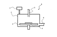
- FIG. 1 is a schematic view of a reaction apparatus 1 used in Examples and Comparative Examples.
- a stage 3 having a function as a heater is installed.
- a heater is also installed around the chamber 2 to heat the chamber wall.
- the dry etching gas composition is supplied to the chamber 2 from a gas supply unit (not shown).
- the dry etching agent can be introduced from the gas inlet 5 installed at the upper portion of the chamber, and the dry etching agent can be brought into contact with the sample 4 installed on the stage 3.
- the gas in the chamber 2 is exhausted via the gas exhaust line 6.
- a vacuum exhaust pump vacuum exhaust unit
- a pressure gauge 7 is installed in the chamber 2.
- Example 1 As a sample 4, a silicon wafer A having a p-Si film, a silicon wafer B having a SiO 2 film, and a silicon wafer C having a SiN film were placed on the stage 3 of the reaction apparatus 1.
- the SiN film and the p-Si film were respectively produced by the CVD method.
- the SiO 2 film was produced by thermally oxidizing the surface of the silicon wafer.
- the temperature of stage 3 was 70.degree.
- a mixed gas of HF and CF 3 COOH HF is 99.9% by volume and CF 3 COOH is 0.1% by volume
- the pressure in the chamber 2 was 10 kPa and etching was performed.
- the etching rate was obtained from the change in thickness of the p-Si film of the silicon wafer A, the SiO 2 film of the silicon wafer B, and the SiN film of the silicon wafer C before and after etching. Further, the ratio of etching rates of SiN and p-Si, SiN / p-Si, and the ratio of etching rates of SiN and SiO 2 , SiN / SiO 2 were determined.
- Ra is the arithmetic mean roughness defined in JIS B 0601: 1994.
- SiN can be selectively etched as compared to p-Si and SiO 2 , and the surface Ra of the SiO 2 film is 1 ⁇ m or less because the surface of the SiO 2 film is hardly scraped. It was very smooth.
- Comparative Example 1 As in Patent Document 2, SiN was etched only with HF, SiO 2 was also scraped, and the SiN / SiO 2 ratio was bad. Similar to Patent Document 3, in Comparative Example 2, F 2 was added to HF to etch SiN, p-Si was etched by F 2 , and the SiN / Si ratio was poor. Comparative Example 3, similarly to Patent Document 4, the addition of NO to the HF and etching the SiN and has damage to the SiO 2 film, the surface of the SiO 2 film after etching was coarser.
- Reactor 2 Chamber 3: Stage 4: Sample 5: Gas inlet 6: Gas exhaust line 7: Pressure gauge
Landscapes
- Chemical & Material Sciences (AREA)
- Engineering & Computer Science (AREA)
- Materials Engineering (AREA)
- Organic Chemistry (AREA)
- Inorganic Chemistry (AREA)
- General Chemical & Material Sciences (AREA)
- Chemical Kinetics & Catalysis (AREA)
- Mechanical Engineering (AREA)
- Metallurgy (AREA)
- Drying Of Semiconductors (AREA)
- Physics & Mathematics (AREA)
- Plasma & Fusion (AREA)
- Crystals, And After-Treatments Of Crystals (AREA)
Abstract
本発明のドライエッチング方法は、窒化ケイ素に、フッ化水素と含フッ素カルボン酸を含む混合ガスを100℃未満かつプラズマレスで接触させ、前記窒化ケイ素をエッチングすることを特徴とする。前記含フッ素カルボン酸の量が、前記フッ化水素と前記含フッ素カルボンの合計の量の0.01体積%以上であることが好ましい。前記含フッ素カルボン酸として、モノフルオロ酢酸、ジフルオロ酢酸、トリフルオロ酢酸、ジフルオロプロピオン酸、ペンタフルオロプロピオン酸、ペンタフルオロ酪酸等を挙げられる。該ドライエッチング方法により、高いエッチングレートで窒化ケイ素をエッチングでき、酸化ケイ素及び多結晶シリコンに対して高い選択比を持ち、酸化ケイ素へのダメージを抑制できる。
Description
本発明は、窒化ケイ素(SiN)をエッチングの対象とした、HFを含むガスによるドライエッチング方法に関する。
半導体デバイスの製造において、単結晶シリコン基板上にて、窒化ケイ素(以下、SiNと呼ぶ)が、酸化ケイ素(以下、SiO2と呼ぶ)及び/又は多結晶シリコン(以下、p-Siと呼ぶ)と隣接する構造から、SiNを選択的にエッチングする工程を行う場合がある。
SiNのエッチング方法としては、熱リン酸を用いたウェットエッチングや、CF4などの化合物ガスから生成されたプラズマを用いたドライエッチングが知られている。
例えば、特許文献1には、SiO2、ケイ化金属又はシリコンの存在下でSiNを選択的にプラズマエッチングするため、式:CHxF4-x(xは2又は3を表す。)で表される化合物のガス及び酸素ガスなどを含むエッチングガスを用いるドライエッチング方法が記載されている。特許文献1では、SiO2膜の開口部からSiN膜を選択的にエッチングし、その下のp-Si膜をエッチング停止層として用いることが記載されている。
しかし、熱リン酸を用いたウェットエッチングや、プラズマを用いたドライエッチングでは、SiNだけでなくSiO2もエッチングしてしまうため、SiNのSiO2に対する選択比を確保することが困難であるという問題点があった。
そこで、特許文献2には、プラズマレスの加熱雰囲気下でHFガスを流通することによってSiO2膜上に形成されたSiN膜をエッチングする方法が記載されている。
また、特許文献3には、特許文献2に記載の方法で課題となるSiO2膜上に形成されたSiN膜のエッチングレートの低さを改善する方法として、HFにF2ガスを添加する方法が記載されている。
しかし、特許文献2のように、SiN膜をHFガスでエッチングすると、HF及び反応生成物であるNH3によって、SiO2膜もエッチングされることがあり、SiN/SiO2の選択比を高くできないといった問題があった。また、特許文献3のように、F2ガスを添加すると、p-SiがF2等によってエッチングされ、SiN/Si選択比が高く取れないという問題があった。
そこで、特許文献4には、HF+NOの混合ガスでSiN膜をSiO2膜及び/又はp-Si膜に対して高選択比でエッチングする方法が記載されており、NOガスをエッチングガス(アシスト用ガス)として添加することで、SiO2膜のダメージを抑えられることが記載されている。
しかしながら、特許文献4において、SiNの選択比を向上する効果は得られても、SiNのエッチングでNH3が副生するため、SiO2へのダメージを十分に抑制することはできなかった。近年の微細化の進展においては、こうしたダメージによる僅かな表面荒れも無視できない問題となりつつあり、この改善が求められている。
なお、SiO2へのダメージ抑制のため、HF+NOなどのエッチングガスにN2やAr、He等の不活性ガスを添加して希釈する方法が考えられる。しかし、この方法では本来目的とするSiNのエッチングレートが大幅に低下することが新たに問題となる。そこで、この低いエッチングレートを補うため、エッチング工程の処理時間を長くし、エッチング量を確保する方法も考えられるが、SiO2がエッチングガスに暴露される時間が長くなるため、結果としてSiO2表面のダメージの進行につながり、この希釈ガスを添加する方法では、本課題の解決には至らなかった。
本発明は、高いエッチングレートでSiNをエッチングでき、シリコン基板上に半導体デバイスを形成する場合には、SiO2やp-Siに対して高い選択比を持ち、さらにSiO2へのダメージも抑制できるドライエッチング方法を提供することを目的とする。
本発明者らは、鋭意検討の結果、含フッ素カルボン酸は、HFによるSiNのエッチングで副生するNH3をトラップできる、SiO2とp-Siをエッチングしない、HFによるSiNのエッチングを阻害しないという特性を持つため、HFにこの含フッ素カルボン酸を混合したガスによってSiNをエッチングすることで、上記課題が解決できることを見出し、本発明を完成させるに至った。
具体的には、本発明は、窒化ケイ素に、フッ化水素と含フッ素カルボン酸を含む混合ガスを100℃未満かつプラズマレスで接触させ、前記窒化ケイ素をエッチングすることを特徴とするドライエッチング方法を提供する。
本発明により、高いエッチングレートでSiNをエッチングでき、シリコン基板上に半導体デバイスを形成する場合には、SiO2及びp-Siに対して高い選択比を持ち、さらにSiO2へのダメージも抑制できるドライエッチング方法を提供できる。
以下、本発明について詳細に説明するが、以下に記載する構成要件の説明は本発明の実施形態の一例であり、これらの具体的内容に限定はされない。その要旨の範囲内で種々変形して実施することができる。
本発明のドライエッチング方法では、フッ化水素と含フッ素カルボン酸を含む混合ガスをドライエッチングガス組成物として用いて、このドライエッチングガス組成物を100℃未満かつプラズマレスで窒化ケイ素に接触させ、窒化ケイ素をエッチングする。
混合ガス中の含フッ素カルボン酸の添加量は、前記フッ化水素と前記含フッ素カルボンの合計の量の0.01体積%以上であることが好ましい。
添加量の上限は各化合物の蒸気圧とプロセス圧力から自ずと決定される。即ち、プロセス圧力が含フッ素カルボン酸の蒸気圧より低い場合、含フッ素カルボン酸の添加量が多くなりHFの濃度が低減するため、HFが不足してSiNのエッチングレートが十分に取れなくなる。そのため、添加量は最大でも、HFと含フッ素カルボン酸の濃度比(HF/含フッ素カルボン酸)が1以上となることが好ましい。
即ち、混合ガス中の含フッ素カルボン酸の添加量は、フッ化水素と前記含フッ素カルボンの合計の量の0.01体積%以上50体積%以下であることが好ましく、0.1体積%以上30体積%以下であることがより好ましく、3体積%以上15体積%以下であることがさらに好ましい。
添加量の上限は各化合物の蒸気圧とプロセス圧力から自ずと決定される。即ち、プロセス圧力が含フッ素カルボン酸の蒸気圧より低い場合、含フッ素カルボン酸の添加量が多くなりHFの濃度が低減するため、HFが不足してSiNのエッチングレートが十分に取れなくなる。そのため、添加量は最大でも、HFと含フッ素カルボン酸の濃度比(HF/含フッ素カルボン酸)が1以上となることが好ましい。
即ち、混合ガス中の含フッ素カルボン酸の添加量は、フッ化水素と前記含フッ素カルボンの合計の量の0.01体積%以上50体積%以下であることが好ましく、0.1体積%以上30体積%以下であることがより好ましく、3体積%以上15体積%以下であることがさらに好ましい。
本発明の方法で使用可能な含フッ素カルボン酸としては、モノフルオロ酢酸(CH2FCOOH)、ジフルオロ酢酸(CHF2COOH)、トリフルオロ酢酸(CF3COOH)、ジフルオロプロピオン酸(CH3CF2COOH)、ペンタフルオロプロピオン酸(C2F5COOH)、ペンタフルオロ酪酸(C3F7COOH)などが挙げられる。これらのガスは、NH3を優先的にトラップするために酸解離定数pKaがHFの3.2以下である点や、20~100℃の温度範囲で一定の蒸気圧を有し、この温度範囲で分解しないためガスとして供給可能である点で好ましい。含フッ素カルボン酸は、加熱、減圧、バブリングにより気化して供給することができる。
また、これらの含フッ素カルボン酸は無水物である必要は無いが、水分量は1質量%未満であることが好ましい。水分量が多いと、気化させた場合にH2Oを生じ、HF+H2OによるSiO2エッチングが発生する可能性があるためである。
また、混合ガスに希釈ガスとしてHFや含フッ素カルボン酸と反応しない不活性ガスを含んでいても良く、不活性ガスの添加量によってSiNのエッチングレートを調整することも可能である。不活性ガスとしては、N2、He、Ne、Ar、Krなどを挙げることができ、混合ガス中に0体積%以上90体積%以下の範囲で使用できる。
窒化ケイ素とドライエッチングガス組成物を接触させるプロセス温度としては、20℃以上100℃未満であることが好ましく、40℃以上80℃以下であることがより好ましく、50℃以上75℃以下であることがさらに好ましい。
プロセス圧力としては、圧力範囲は0.1kPa以上101.3kPa以下が好ましく、1kPa以上50kPa以下がより好ましい。
なお、本発明のエッチング対象である窒化ケイ素としては、Si3N4等のSiNx(xは0超、2以下)で表される化合物を意味する。
本発明のドライエッチングガス組成物を、窒化ケイ素と酸化ケイ素と多結晶シリコンに接触させた場合、SiNとSiO2のエッチング選択比(SiN/SiO2)と、SiNとp-Siのエッチング選択比(SiN/Si)がいずれも100以上であることが好ましい。また、SiNに対して100nm/min以上の高いエッチングレートを有することが好ましい。
本発明のエッチング方法により、SiO2やp-Siにダメージを与えることなく、高速かつ高選択的にSiNをエッチングすることができる。更に、本発明のエッチング方法は、100℃未満の低温、かつプラズマレスのプロセスで実施可能である。
また、SiNのエッチングによって副生するNH3は、HFと反応してNH4Fを生成する副反応も生じるため、SiN表面でのHF濃度を低減させ、エッチング速度の低下につながる要因となる。しかし、本発明のエッチング方法では、含フッ素カルボン酸を混合することにより、この副反応を防止し、エッチング速度の低下を防止する効果が期待できる。
更に、HF中に微量の水分が含まれている、あるいは、SiO2表面に吸着する水が存在した場合、この微量水分とHFによってSiO2のエッチングが進行することがある。しかし、本発明のエッチング方法では、含フッ素カルボン酸を添加することにより、この微量水分を含フッ素カルボン酸で除去でき、SiO2のエッチングを更に防止する効果も期待できる。
シリコン基板上に半導体デバイスを形成する場合に、SiNがSiO2及び/又はp-Siに隣接する構造や、SiO2及び/又はp-Siと、SiNとが露出した構造からSiNのみを選択的にドライエッチングする工程に、本発明のドライエッチング方法を適用することができる。このような構造としては、SiO2膜及び/又はp-Si膜をSiN膜が覆う構造や、SiO2膜とSiN膜とp-Si膜が積層した構造などがある。例えば、3次元メモリの製造プロセスにおいて、シリコン基板に、SiO2とSiNの積層膜を形成し、この積層膜に貫通孔を形成し、貫通孔からエッチングガスを供給して本発明のドライエッチング方法を適用して、SiO2を残しながらSiNを選択的にエッチングすることで、多数のSiO2層が間隙を有しつつ平行に並んだ構造を形成することができる。
以下に本発明の実施例を比較例とともに挙げるが、本発明は以下の実施例に制限されるものではない。
図1は、実施例・比較例で用いた反応装置1の概略図である、チャンバー2内には、ヒーターとしての機能を有するステージ3が設置されている。また、チャンバー2の周囲にもヒーターが設置されており、チャンバー壁を加熱できるようになっている。チャンバー2には、図示しないガス供給部からドライエッチングガス組成物が供給される。チャンバー上部に設置されたガス導入口5からドライエッチング剤を導入し、ステージ3上に設置した試料4に対しドライエッチング剤を接触させることができる。チャンバー2内のガスはガス排出ライン6を経由して排出される。また、ガス排出ラインには図示しない真空排気ポンプ(真空排気部)が接続され、チャンバー2内は減圧環境にすることができ、チャンバー2には圧力計7が設置されている。
[実施例1]
試料4として、p-Si膜を有するシリコンウエハA、SiO2膜を有するシリコンウエハB、SiN膜を有するシリコンウエハCを反応装置1のステージ3上に設置した。SiN膜とp-Si膜は、それぞれCVD法により作製した。また、SiO2膜はシリコンウエハの表面を熱酸化して作製した。ステージ3の温度は70℃であった。ここに、HFとCF3COOHの混合ガス(HFが99.9体積%で、CF3COOHが0.1体積%である)を、総流量1000sccmとして流通させた。チャンバー2内圧力は10kPaとし、エッチングを行った。
試料4として、p-Si膜を有するシリコンウエハA、SiO2膜を有するシリコンウエハB、SiN膜を有するシリコンウエハCを反応装置1のステージ3上に設置した。SiN膜とp-Si膜は、それぞれCVD法により作製した。また、SiO2膜はシリコンウエハの表面を熱酸化して作製した。ステージ3の温度は70℃であった。ここに、HFとCF3COOHの混合ガス(HFが99.9体積%で、CF3COOHが0.1体積%である)を、総流量1000sccmとして流通させた。チャンバー2内圧力は10kPaとし、エッチングを行った。
エッチング後に、シリコンウエハAのp-Si膜、シリコンウエハBのSiO2膜、シリコンウエハCのSiN膜の、エッチング前後の厚さの変化からエッチング速度を求めた。さらに、SiNとp-Siのエッチング速度の比SiN/p-Siと、SiNとSiO2のエッチング速度の比SiN/SiO2を求めた。
また、SiO2膜の表面粗さRaを、原子間力顕微鏡(AFM)で測定して評価した。ここで、Raとは、JIS B 0601:1994にて規定される算術平均粗さのことである。
[実施例2~5、比較例1~3]
添加ガスの種類と濃度を変更した以外は、実施例1と同様にエッチング及び評価を行った。
添加ガスの種類と濃度を変更した以外は、実施例1と同様にエッチング及び評価を行った。
実施例1~5及び比較例1~3のエッチング条件及び評価結果を表1に示す。

実施例1~5では、p-SiとSiO2に比べて、SiNを選択的にエッチングすることができ、SiO2膜の表面をほとんど削らなかったためにSiO2膜の表面Raが1μm以下となり、非常に滑らかであった。
一方、比較例1は、特許文献2と同様に、HFのみでSiNをエッチングしており、SiO2も削れてしまい、SiN/SiO2比が悪かった。比較例2は、特許文献3と同様に、HFにF2を添加してSiNをエッチングしており、F2によりp-Siがエッチングされ、SiN/Si比が悪かった。比較例3は、特許文献4と同様に、HFにNOを添加してSiNをエッチングしており、SiO2膜へのダメージがあり、エッチング後のSiO2膜の表面が粗かった。
1: 反応装置
2: チャンバー
3: ステージ
4: 試料
5: ガス導入口
6: ガス排出ライン
7: 圧力計
2: チャンバー
3: ステージ
4: 試料
5: ガス導入口
6: ガス排出ライン
7: 圧力計
Claims (10)
- 窒化ケイ素に、フッ化水素と含フッ素カルボン酸を含む混合ガスを100℃未満かつプラズマレスで接触させ、前記窒化ケイ素をエッチングすることを特徴とするドライエッチング方法。
- 前記含フッ素カルボン酸の量が、前記フッ化水素と前記含フッ素カルボンの合計の量の0.01体積%以上であることを特徴とする請求項1に記載のドライエッチング方法。
- 前記含フッ素カルボン酸が、モノフルオロ酢酸、ジフルオロ酢酸、トリフルオロ酢酸、ジフルオロプロピオン酸、ペンタフルオロプロピオン酸、及びペンタフルオロ酪酸からなる群から選ばれる少なくとも一種であることを特徴とする請求項1または2に記載のドライエッチング方法。
- 前記混合ガスが、前記窒化ケイ素だけでなく、酸化ケイ素及び多結晶シリコンにも接触し、
前記窒化ケイ素と前記酸化ケイ素のエッチング選択比(SiN/SiO2)と、前記窒化ケイ素と前記多結晶シリコンのエッチング選択比(SiN/Si)がいずれも100以上であることを特徴とする請求項1に記載のドライエッチング方法。 - 前記含フッ素カルボン酸が、トリフルオロ酢酸又はペンタフルオロプロピオン酸であり、
前記含フッ素カルボン酸の量が、前記フッ化水素と前記含フッ素カルボンの合計の量の0.1体積%以上30体積%以下である
ことを特徴とする請求項1に記載のドライエッチング方法。 - 酸化ケイ素膜、多結晶シリコン膜及び窒化ケイ素膜を有するシリコン基板に対して、請求項1~5のいずれかに記載のドライエッチング方法を適用して、選択的に窒化ケイ素膜をエッチングする工程を含むことを特徴とする半導体デバイスの製造方法。
- フッ化水素と含フッ素カルボン酸を含むドライエッチングガス組成物。
- 実質的にフッ化水素と含フッ素カルボン酸のみからなる請求項7に記載のドライエッチングガス組成物。
- 前記含フッ素カルボン酸の量が、前記フッ化水素と前記含フッ素カルボンの合計の量の0.01体積%以上であることを特徴とする請求項7または8に記載のドライエッチングガス組成物。
- 窒化ケイ素膜を有するシリコン基板を載置するステージを有するチャンバーと、
前記ステージに載置された前記基板に対して、フッ化水素と含フッ素カルボン酸を含むドライエッチングガス組成物を供給するためのガス供給部と、
前記チャンバー内を減圧するための真空排気部と、
前記ステージを加熱するためのヒーターと、
を備える、前記基板から前記窒化ケイ素膜をエッチングするエッチング装置。
Priority Applications (4)
| Application Number | Priority Date | Filing Date | Title |
|---|---|---|---|
| KR1020207015097A KR102419013B1 (ko) | 2017-11-14 | 2018-10-24 | 드라이에칭 방법 |
| CN201880068626.2A CN111279460B (zh) | 2017-11-14 | 2018-10-24 | 干式蚀刻方法 |
| US16/762,790 US11289340B2 (en) | 2017-11-14 | 2018-10-24 | Dry etching method |
| US17/677,367 US12387940B2 (en) | 2017-11-14 | 2022-02-22 | Dry etching method |
Applications Claiming Priority (2)
| Application Number | Priority Date | Filing Date | Title |
|---|---|---|---|
| JP2017-218692 | 2017-11-14 | ||
| JP2017218692 | 2017-11-14 |
Related Child Applications (2)
| Application Number | Title | Priority Date | Filing Date |
|---|---|---|---|
| US16/762,790 A-371-Of-International US11289340B2 (en) | 2017-11-14 | 2018-10-24 | Dry etching method |
| US17/677,367 Division US12387940B2 (en) | 2017-11-14 | 2022-02-22 | Dry etching method |
Publications (1)
| Publication Number | Publication Date |
|---|---|
| WO2019097964A1 true WO2019097964A1 (ja) | 2019-05-23 |
Family
ID=66539502
Family Applications (1)
| Application Number | Title | Priority Date | Filing Date |
|---|---|---|---|
| PCT/JP2018/039406 Ceased WO2019097964A1 (ja) | 2017-11-14 | 2018-10-24 | ドライエッチング方法 |
Country Status (6)
| Country | Link |
|---|---|
| US (2) | US11289340B2 (ja) |
| JP (2) | JP7177344B2 (ja) |
| KR (1) | KR102419013B1 (ja) |
| CN (1) | CN111279460B (ja) |
| TW (2) | TWI765114B (ja) |
| WO (1) | WO2019097964A1 (ja) |
Cited By (1)
| Publication number | Priority date | Publication date | Assignee | Title |
|---|---|---|---|---|
| CN116169018A (zh) * | 2019-11-08 | 2023-05-26 | 东京毅力科创株式会社 | 蚀刻方法 |
Families Citing this family (8)
| Publication number | Priority date | Publication date | Assignee | Title |
|---|---|---|---|---|
| KR20230132361A (ko) | 2021-01-25 | 2023-09-15 | 램 리써치 코포레이션 | 열적 에칭에 의한 선택적인 실리콘 트리밍 |
| WO2022176142A1 (ja) * | 2021-02-19 | 2022-08-25 | 株式会社日立ハイテク | エッチング方法およびエッチング装置 |
| US11295960B1 (en) * | 2021-03-09 | 2022-04-05 | Hitachi High-Tech Corporation | Etching method |
| JP2025508876A (ja) * | 2022-03-03 | 2025-04-10 | ラム リサーチ コーポレーション | 半導体材料の選択的精密エッチング |
| US20250232983A1 (en) | 2022-06-16 | 2025-07-17 | Central Glass Company, Limited | Etching method, method for producing semiconductor device, etching apparatus and etching gas |
| CN118525355A (zh) | 2022-12-19 | 2024-08-20 | 株式会社日立高新技术 | 蚀刻方法 |
| KR20250117360A (ko) | 2024-01-22 | 2025-08-04 | 주식회사 히타치하이테크 | 에칭 방법 |
| JP2026049640A (ja) * | 2024-09-06 | 2026-03-18 | ダイキン工業株式会社 | エッチング方法 |
Citations (10)
| Publication number | Priority date | Publication date | Assignee | Title |
|---|---|---|---|---|
| JPH09181054A (ja) * | 1995-11-17 | 1997-07-11 | Air Prod And Chem Inc | トリフルオロ酢酸及びその誘導体を使用するプラズマエッチング法 |
| JPH09509531A (ja) * | 1993-05-13 | 1997-09-22 | インターユニヴァーシテアー マイクロエレクトロニカ セントラム フェレニギング ゾンデル ビンシュトベヤーク | Hf及びカルボン酸の混合物を用いた半導体処理の方法 |
| JP2000058505A (ja) * | 1998-06-09 | 2000-02-25 | Air Prod And Chem Inc | シリコンからのSiO2/金属の気相除去 |
| US6221680B1 (en) * | 1998-07-31 | 2001-04-24 | International Business Machines Corporation | Patterned recess formation using acid diffusion |
| JP2002158181A (ja) * | 2000-09-11 | 2002-05-31 | Research Institute Of Innovative Technology For The Earth | クリーニングガス及びエッチングガス |
| JP2009043973A (ja) * | 2007-08-09 | 2009-02-26 | Tokyo Electron Ltd | 半導体装置の製造方法、半導体基板の処理装置及び記憶媒体 |
| JP2009129980A (ja) * | 2007-11-20 | 2009-06-11 | Tokyo Electron Ltd | 基板処理方法および半導体装置の製造方法、コンピュータ可読記録媒体 |
| JP2010509777A (ja) * | 2006-11-07 | 2010-03-25 | アドバンスド テクノロジー マテリアルズ,インコーポレイテッド | メモリデバイス構造の洗浄製剤 |
| JP2011119310A (ja) * | 2009-12-01 | 2011-06-16 | Central Glass Co Ltd | エッチングガス |
| WO2017091572A1 (en) * | 2015-11-23 | 2017-06-01 | Entegris, Inc. | Composition and process for selectively etching p-doped polysilicon relative to silicon nitride |
Family Cites Families (12)
| Publication number | Priority date | Publication date | Assignee | Title |
|---|---|---|---|---|
| JPH06163476A (ja) * | 1992-11-18 | 1994-06-10 | Sony Corp | ドライエッチング方法 |
| US5922624A (en) | 1993-05-13 | 1999-07-13 | Imec Vzw | Method for semiconductor processing using mixtures of HF and carboxylic acid |
| KR950033669A (ko) | 1994-01-27 | 1995-12-26 | 제임스 조셉 드롱 | 산화물, 규화물 및 실리콘에 대하여 선택성을 갖는 질화물 식각공정 |
| US5626775A (en) | 1996-05-13 | 1997-05-06 | Air Products And Chemicals, Inc. | Plasma etch with trifluoroacetic acid and derivatives |
| US6140203A (en) * | 1997-10-31 | 2000-10-31 | Micron Technology, Inc. | Capacitor constructions and semiconductor processing method of forming capacitor constructions |
| JPH11238725A (ja) * | 1998-02-24 | 1999-08-31 | Daikin Ind Ltd | エッチング組成物 |
| KR100649418B1 (ko) * | 2002-08-22 | 2006-11-27 | 다이킨 고교 가부시키가이샤 | 박리액 |
| US7214978B2 (en) * | 2004-02-27 | 2007-05-08 | Micron Technology, Inc. | Semiconductor fabrication that includes surface tension control |
| US20070207622A1 (en) * | 2006-02-23 | 2007-09-06 | Micron Technology, Inc. | Highly selective doped oxide etchant |
| JP4833878B2 (ja) | 2007-01-31 | 2011-12-07 | 東京エレクトロン株式会社 | 基板の処理方法及び基板処理装置 |
| JP5210191B2 (ja) | 2009-02-03 | 2013-06-12 | 東京エレクトロン株式会社 | 窒化珪素膜のドライエッチング方法 |
| JP6073172B2 (ja) | 2013-03-29 | 2017-02-01 | 岩谷産業株式会社 | エッチング方法 |
-
2018
- 2018-10-19 JP JP2018197338A patent/JP7177344B2/ja active Active
- 2018-10-24 US US16/762,790 patent/US11289340B2/en active Active
- 2018-10-24 WO PCT/JP2018/039406 patent/WO2019097964A1/ja not_active Ceased
- 2018-10-24 CN CN201880068626.2A patent/CN111279460B/zh active Active
- 2018-10-24 KR KR1020207015097A patent/KR102419013B1/ko active Active
- 2018-11-05 TW TW107139099A patent/TWI765114B/zh active
- 2018-11-05 TW TW111114223A patent/TWI824482B/zh active
-
2022
- 2022-02-22 US US17/677,367 patent/US12387940B2/en active Active
- 2022-11-09 JP JP2022179702A patent/JP7332961B2/ja active Active
Patent Citations (10)
| Publication number | Priority date | Publication date | Assignee | Title |
|---|---|---|---|---|
| JPH09509531A (ja) * | 1993-05-13 | 1997-09-22 | インターユニヴァーシテアー マイクロエレクトロニカ セントラム フェレニギング ゾンデル ビンシュトベヤーク | Hf及びカルボン酸の混合物を用いた半導体処理の方法 |
| JPH09181054A (ja) * | 1995-11-17 | 1997-07-11 | Air Prod And Chem Inc | トリフルオロ酢酸及びその誘導体を使用するプラズマエッチング法 |
| JP2000058505A (ja) * | 1998-06-09 | 2000-02-25 | Air Prod And Chem Inc | シリコンからのSiO2/金属の気相除去 |
| US6221680B1 (en) * | 1998-07-31 | 2001-04-24 | International Business Machines Corporation | Patterned recess formation using acid diffusion |
| JP2002158181A (ja) * | 2000-09-11 | 2002-05-31 | Research Institute Of Innovative Technology For The Earth | クリーニングガス及びエッチングガス |
| JP2010509777A (ja) * | 2006-11-07 | 2010-03-25 | アドバンスド テクノロジー マテリアルズ,インコーポレイテッド | メモリデバイス構造の洗浄製剤 |
| JP2009043973A (ja) * | 2007-08-09 | 2009-02-26 | Tokyo Electron Ltd | 半導体装置の製造方法、半導体基板の処理装置及び記憶媒体 |
| JP2009129980A (ja) * | 2007-11-20 | 2009-06-11 | Tokyo Electron Ltd | 基板処理方法および半導体装置の製造方法、コンピュータ可読記録媒体 |
| JP2011119310A (ja) * | 2009-12-01 | 2011-06-16 | Central Glass Co Ltd | エッチングガス |
| WO2017091572A1 (en) * | 2015-11-23 | 2017-06-01 | Entegris, Inc. | Composition and process for selectively etching p-doped polysilicon relative to silicon nitride |
Cited By (1)
| Publication number | Priority date | Publication date | Assignee | Title |
|---|---|---|---|---|
| CN116169018A (zh) * | 2019-11-08 | 2023-05-26 | 东京毅力科创株式会社 | 蚀刻方法 |
Also Published As
| Publication number | Publication date |
|---|---|
| JP2019091890A (ja) | 2019-06-13 |
| CN111279460B (zh) | 2023-07-18 |
| KR102419013B1 (ko) | 2022-07-08 |
| CN111279460A (zh) | 2020-06-12 |
| US12387940B2 (en) | 2025-08-12 |
| TW202229515A (zh) | 2022-08-01 |
| TW201923039A (zh) | 2019-06-16 |
| KR20200070382A (ko) | 2020-06-17 |
| JP7177344B2 (ja) | 2022-11-24 |
| JP2023001302A (ja) | 2023-01-04 |
| TWI765114B (zh) | 2022-05-21 |
| US11289340B2 (en) | 2022-03-29 |
| US20220172956A1 (en) | 2022-06-02 |
| TWI824482B (zh) | 2023-12-01 |
| JP7332961B2 (ja) | 2023-08-24 |
| US20200365411A1 (en) | 2020-11-19 |
Similar Documents
| Publication | Publication Date | Title |
|---|---|---|
| JP7332961B2 (ja) | ドライエッチング方法 | |
| TWI525658B (zh) | 設計製造用於微影蝕刻遮罩應用的富硼薄膜之方法 | |
| CN108573866B (zh) | 氧化膜去除方法和装置以及接触部形成方法和系统 | |
| CN100377317C (zh) | 硅氧化膜的去除方法及处理装置 | |
| JP2019212872A (ja) | エッチング方法およびエッチング装置 | |
| JP6280655B2 (ja) | ケイ素化合物用エッチングガス組成物及びエッチング方法 | |
| US12100601B2 (en) | Etching method with metal hard mask | |
| JP4039385B2 (ja) | ケミカル酸化膜の除去方法 | |
| TW201903828A (zh) | 氧化膜去除方法及去除裝置、接觸部形成方法及接觸部形成系統、以及記憶媒體 | |
| KR20210023906A (ko) | 황 원자를 함유하는 가스 분자를 사용한 플라즈마 에칭 방법 | |
| KR100685735B1 (ko) | 폴리실리콘 제거용 조성물, 이를 이용한 폴리실리콘 제거방법 및 반도체 장치의 제조 방법 | |
| US8541307B2 (en) | Treatment method for reducing particles in dual damascene silicon nitride process | |
| JP2010098101A (ja) | 半導体装置の製造方法 | |
| KR20250024985A (ko) | 에칭 방법, 반도체 디바이스의 제조 방법, 에칭 장치 및 에칭 가스 | |
| CN117577517B (zh) | 一种复合衬底清洗方法 | |
| TWI913690B (zh) | 使用含矽氫氟烴之蝕刻方法 | |
| TWI914748B (zh) | 使用含矽氫氟烴之蝕刻方法 | |
| TWI921757B (zh) | 使用含矽氫氟烴之蝕刻方法 | |
| TWI914747B (zh) | 使用含矽氫氟烴之蝕刻方法 | |
| CN103035509A (zh) | 半导体器件的制造方法 | |
| TW202527107A (zh) | 基板製程方法 | |
| WO2025052986A1 (ja) | 基材の処理方法および基材の製造方法 | |
| TW202604853A (zh) | 蝕刻方法、半導體裝置之製造方法、蝕刻裝置及蝕刻氣體組合物 | |
| KR100361859B1 (ko) | 반도체소자의산화막식각방법 | |
| JP2002009038A (ja) | 半導体基板の処理方法 |
Legal Events
| Date | Code | Title | Description |
|---|---|---|---|
| 121 | Ep: the epo has been informed by wipo that ep was designated in this application |
Ref document number: 18879889 Country of ref document: EP Kind code of ref document: A1 |
|
| NENP | Non-entry into the national phase |
Ref country code: DE |
|
| ENP | Entry into the national phase |
Ref document number: 20207015097 Country of ref document: KR Kind code of ref document: A |
|
| 122 | Ep: pct application non-entry in european phase |
Ref document number: 18879889 Country of ref document: EP Kind code of ref document: A1 |