WO2019065309A1 - ボンディングの際の半導体チップの加熱条件設定方法及び非導電性フィルムの粘度測定方法ならびにボンディング装置 - Google Patents
ボンディングの際の半導体チップの加熱条件設定方法及び非導電性フィルムの粘度測定方法ならびにボンディング装置 Download PDFInfo
- Publication number
- WO2019065309A1 WO2019065309A1 PCT/JP2018/034203 JP2018034203W WO2019065309A1 WO 2019065309 A1 WO2019065309 A1 WO 2019065309A1 JP 2018034203 W JP2018034203 W JP 2018034203W WO 2019065309 A1 WO2019065309 A1 WO 2019065309A1
- Authority
- WO
- WIPO (PCT)
- Prior art keywords
- temperature
- bonding
- viscosity
- semiconductor chip
- heating
- Prior art date
- Legal status (The legal status is an assumption and is not a legal conclusion. Google has not performed a legal analysis and makes no representation as to the accuracy of the status listed.)
- Ceased
Links
Images



Classifications
-
- H—ELECTRICITY
- H10—SEMICONDUCTOR DEVICES; ELECTRIC SOLID-STATE DEVICES NOT OTHERWISE PROVIDED FOR
- H10W—GENERIC PACKAGES, INTERCONNECTIONS, CONNECTORS OR OTHER CONSTRUCTIONAL DETAILS OF DEVICES COVERED BY CLASS H10
- H10W90/00—Package configurations
-
- H—ELECTRICITY
- H10—SEMICONDUCTOR DEVICES; ELECTRIC SOLID-STATE DEVICES NOT OTHERWISE PROVIDED FOR
- H10W—GENERIC PACKAGES, INTERCONNECTIONS, CONNECTORS OR OTHER CONSTRUCTIONAL DETAILS OF DEVICES COVERED BY CLASS H10
- H10W72/00—Interconnections or connectors in packages
- H10W72/071—Connecting or disconnecting
- H10W72/0711—Apparatus therefor
-
- H—ELECTRICITY
- H10—SEMICONDUCTOR DEVICES; ELECTRIC SOLID-STATE DEVICES NOT OTHERWISE PROVIDED FOR
- H10W—GENERIC PACKAGES, INTERCONNECTIONS, CONNECTORS OR OTHER CONSTRUCTIONAL DETAILS OF DEVICES COVERED BY CLASS H10
- H10W72/00—Interconnections or connectors in packages
- H10W72/071—Connecting or disconnecting
- H10W72/072—Connecting or disconnecting of bump connectors
-
- H—ELECTRICITY
- H10—SEMICONDUCTOR DEVICES; ELECTRIC SOLID-STATE DEVICES NOT OTHERWISE PROVIDED FOR
- H10W—GENERIC PACKAGES, INTERCONNECTIONS, CONNECTORS OR OTHER CONSTRUCTIONAL DETAILS OF DEVICES COVERED BY CLASS H10
- H10W72/00—Interconnections or connectors in packages
- H10W72/20—Bump connectors, e.g. solder bumps or copper pillars; Dummy bumps; Thermal bumps
-
- H—ELECTRICITY
- H10—SEMICONDUCTOR DEVICES; ELECTRIC SOLID-STATE DEVICES NOT OTHERWISE PROVIDED FOR
- H10W—GENERIC PACKAGES, INTERCONNECTIONS, CONNECTORS OR OTHER CONSTRUCTIONAL DETAILS OF DEVICES COVERED BY CLASS H10
- H10W72/00—Interconnections or connectors in packages
- H10W72/30—Die-attach connectors
-
- H—ELECTRICITY
- H10—SEMICONDUCTOR DEVICES; ELECTRIC SOLID-STATE DEVICES NOT OTHERWISE PROVIDED FOR
- H10W—GENERIC PACKAGES, INTERCONNECTIONS, CONNECTORS OR OTHER CONSTRUCTIONAL DETAILS OF DEVICES COVERED BY CLASS H10
- H10W72/00—Interconnections or connectors in packages
- H10W72/851—Dispositions of multiple connectors or interconnections
-
- H—ELECTRICITY
- H10—SEMICONDUCTOR DEVICES; ELECTRIC SOLID-STATE DEVICES NOT OTHERWISE PROVIDED FOR
- H10P—GENERIC PROCESSES OR APPARATUS FOR THE MANUFACTURE OR TREATMENT OF DEVICES COVERED BY CLASS H10
- H10P74/00—Testing or measuring during manufacture or treatment of wafers, substrates or devices
- H10P74/23—Testing or measuring during manufacture or treatment of wafers, substrates or devices characterised by multiple measurements, corrections, marking or sorting processes
-
- H—ELECTRICITY
- H10—SEMICONDUCTOR DEVICES; ELECTRIC SOLID-STATE DEVICES NOT OTHERWISE PROVIDED FOR
- H10P—GENERIC PROCESSES OR APPARATUS FOR THE MANUFACTURE OR TREATMENT OF DEVICES COVERED BY CLASS H10
- H10P74/00—Testing or measuring during manufacture or treatment of wafers, substrates or devices
- H10P74/23—Testing or measuring during manufacture or treatment of wafers, substrates or devices characterised by multiple measurements, corrections, marking or sorting processes
- H10P74/238—Testing or measuring during manufacture or treatment of wafers, substrates or devices characterised by multiple measurements, corrections, marking or sorting processes comprising acting in response to an ongoing measurement without interruption of processing, e.g. endpoint detection or in-situ thickness measurement
-
- H—ELECTRICITY
- H10—SEMICONDUCTOR DEVICES; ELECTRIC SOLID-STATE DEVICES NOT OTHERWISE PROVIDED FOR
- H10W—GENERIC PACKAGES, INTERCONNECTIONS, CONNECTORS OR OTHER CONSTRUCTIONAL DETAILS OF DEVICES COVERED BY CLASS H10
- H10W72/00—Interconnections or connectors in packages
- H10W72/01—Manufacture or treatment
- H10W72/016—Manufacture or treatment of strap connectors
-
- H—ELECTRICITY
- H10—SEMICONDUCTOR DEVICES; ELECTRIC SOLID-STATE DEVICES NOT OTHERWISE PROVIDED FOR
- H10W—GENERIC PACKAGES, INTERCONNECTIONS, CONNECTORS OR OTHER CONSTRUCTIONAL DETAILS OF DEVICES COVERED BY CLASS H10
- H10W72/00—Interconnections or connectors in packages
- H10W72/071—Connecting or disconnecting
- H10W72/0711—Apparatus therefor
- H10W72/07141—Means for applying energy, e.g. ovens or lasers
-
- H—ELECTRICITY
- H10—SEMICONDUCTOR DEVICES; ELECTRIC SOLID-STATE DEVICES NOT OTHERWISE PROVIDED FOR
- H10W—GENERIC PACKAGES, INTERCONNECTIONS, CONNECTORS OR OTHER CONSTRUCTIONAL DETAILS OF DEVICES COVERED BY CLASS H10
- H10W72/00—Interconnections or connectors in packages
- H10W72/071—Connecting or disconnecting
- H10W72/0711—Apparatus therefor
- H10W72/07178—Means for aligning
-
- H—ELECTRICITY
- H10—SEMICONDUCTOR DEVICES; ELECTRIC SOLID-STATE DEVICES NOT OTHERWISE PROVIDED FOR
- H10W—GENERIC PACKAGES, INTERCONNECTIONS, CONNECTORS OR OTHER CONSTRUCTIONAL DETAILS OF DEVICES COVERED BY CLASS H10
- H10W72/00—Interconnections or connectors in packages
- H10W72/071—Connecting or disconnecting
- H10W72/0711—Apparatus therefor
- H10W72/07183—Means for monitoring
-
- H—ELECTRICITY
- H10—SEMICONDUCTOR DEVICES; ELECTRIC SOLID-STATE DEVICES NOT OTHERWISE PROVIDED FOR
- H10W—GENERIC PACKAGES, INTERCONNECTIONS, CONNECTORS OR OTHER CONSTRUCTIONAL DETAILS OF DEVICES COVERED BY CLASS H10
- H10W72/00—Interconnections or connectors in packages
- H10W72/071—Connecting or disconnecting
- H10W72/072—Connecting or disconnecting of bump connectors
- H10W72/07231—Techniques
- H10W72/07236—Soldering or alloying
-
- H—ELECTRICITY
- H10—SEMICONDUCTOR DEVICES; ELECTRIC SOLID-STATE DEVICES NOT OTHERWISE PROVIDED FOR
- H10W—GENERIC PACKAGES, INTERCONNECTIONS, CONNECTORS OR OTHER CONSTRUCTIONAL DETAILS OF DEVICES COVERED BY CLASS H10
- H10W72/00—Interconnections or connectors in packages
- H10W72/071—Connecting or disconnecting
- H10W72/073—Connecting or disconnecting of die-attach connectors
-
- H—ELECTRICITY
- H10—SEMICONDUCTOR DEVICES; ELECTRIC SOLID-STATE DEVICES NOT OTHERWISE PROVIDED FOR
- H10W—GENERIC PACKAGES, INTERCONNECTIONS, CONNECTORS OR OTHER CONSTRUCTIONAL DETAILS OF DEVICES COVERED BY CLASS H10
- H10W72/00—Interconnections or connectors in packages
- H10W72/071—Connecting or disconnecting
- H10W72/073—Connecting or disconnecting of die-attach connectors
- H10W72/07331—Connecting techniques
-
- H—ELECTRICITY
- H10—SEMICONDUCTOR DEVICES; ELECTRIC SOLID-STATE DEVICES NOT OTHERWISE PROVIDED FOR
- H10W—GENERIC PACKAGES, INTERCONNECTIONS, CONNECTORS OR OTHER CONSTRUCTIONAL DETAILS OF DEVICES COVERED BY CLASS H10
- H10W72/00—Interconnections or connectors in packages
- H10W72/071—Connecting or disconnecting
- H10W72/073—Connecting or disconnecting of die-attach connectors
- H10W72/07331—Connecting techniques
- H10W72/07332—Compression bonding, e.g. thermocompression bonding
-
- H—ELECTRICITY
- H10—SEMICONDUCTOR DEVICES; ELECTRIC SOLID-STATE DEVICES NOT OTHERWISE PROVIDED FOR
- H10W—GENERIC PACKAGES, INTERCONNECTIONS, CONNECTORS OR OTHER CONSTRUCTIONAL DETAILS OF DEVICES COVERED BY CLASS H10
- H10W72/00—Interconnections or connectors in packages
- H10W72/071—Connecting or disconnecting
- H10W72/073—Connecting or disconnecting of die-attach connectors
- H10W72/07331—Connecting techniques
- H10W72/07337—Connecting techniques using a polymer adhesive, e.g. an adhesive based on silicone or epoxy
- H10W72/07338—Connecting techniques using a polymer adhesive, e.g. an adhesive based on silicone or epoxy hardening the adhesive by curing, e.g. thermosetting
-
- H—ELECTRICITY
- H10—SEMICONDUCTOR DEVICES; ELECTRIC SOLID-STATE DEVICES NOT OTHERWISE PROVIDED FOR
- H10W—GENERIC PACKAGES, INTERCONNECTIONS, CONNECTORS OR OTHER CONSTRUCTIONAL DETAILS OF DEVICES COVERED BY CLASS H10
- H10W72/00—Interconnections or connectors in packages
- H10W72/071—Connecting or disconnecting
- H10W72/073—Connecting or disconnecting of die-attach connectors
- H10W72/07341—Controlling the bonding environment, e.g. atmosphere composition or temperature
-
- H—ELECTRICITY
- H10—SEMICONDUCTOR DEVICES; ELECTRIC SOLID-STATE DEVICES NOT OTHERWISE PROVIDED FOR
- H10W—GENERIC PACKAGES, INTERCONNECTIONS, CONNECTORS OR OTHER CONSTRUCTIONAL DETAILS OF DEVICES COVERED BY CLASS H10
- H10W72/00—Interconnections or connectors in packages
- H10W72/20—Bump connectors, e.g. solder bumps or copper pillars; Dummy bumps; Thermal bumps
- H10W72/251—Materials
- H10W72/252—Materials comprising solid metals or solid metalloids, e.g. PbSn, Ag or Cu
-
- H—ELECTRICITY
- H10—SEMICONDUCTOR DEVICES; ELECTRIC SOLID-STATE DEVICES NOT OTHERWISE PROVIDED FOR
- H10W—GENERIC PACKAGES, INTERCONNECTIONS, CONNECTORS OR OTHER CONSTRUCTIONAL DETAILS OF DEVICES COVERED BY CLASS H10
- H10W74/00—Encapsulations, e.g. protective coatings
- H10W74/01—Manufacture or treatment
- H10W74/012—Manufacture or treatment of encapsulations on active surfaces of flip-chip devices, e.g. forming underfills
-
- H—ELECTRICITY
- H10—SEMICONDUCTOR DEVICES; ELECTRIC SOLID-STATE DEVICES NOT OTHERWISE PROVIDED FOR
- H10W—GENERIC PACKAGES, INTERCONNECTIONS, CONNECTORS OR OTHER CONSTRUCTIONAL DETAILS OF DEVICES COVERED BY CLASS H10
- H10W74/00—Encapsulations, e.g. protective coatings
- H10W74/10—Encapsulations, e.g. protective coatings characterised by their shape or disposition
- H10W74/15—Encapsulations, e.g. protective coatings characterised by their shape or disposition on active surfaces of flip-chip devices, e.g. underfills
-
- H—ELECTRICITY
- H10—SEMICONDUCTOR DEVICES; ELECTRIC SOLID-STATE DEVICES NOT OTHERWISE PROVIDED FOR
- H10W—GENERIC PACKAGES, INTERCONNECTIONS, CONNECTORS OR OTHER CONSTRUCTIONAL DETAILS OF DEVICES COVERED BY CLASS H10
- H10W90/00—Package configurations
- H10W90/701—Package configurations characterised by the relative positions of pads or connectors relative to package parts
- H10W90/721—Package configurations characterised by the relative positions of pads or connectors relative to package parts of bump connectors
- H10W90/722—Package configurations characterised by the relative positions of pads or connectors relative to package parts of bump connectors between stacked chips
-
- H—ELECTRICITY
- H10—SEMICONDUCTOR DEVICES; ELECTRIC SOLID-STATE DEVICES NOT OTHERWISE PROVIDED FOR
- H10W—GENERIC PACKAGES, INTERCONNECTIONS, CONNECTORS OR OTHER CONSTRUCTIONAL DETAILS OF DEVICES COVERED BY CLASS H10
- H10W90/00—Package configurations
- H10W90/701—Package configurations characterised by the relative positions of pads or connectors relative to package parts
- H10W90/721—Package configurations characterised by the relative positions of pads or connectors relative to package parts of bump connectors
- H10W90/724—Package configurations characterised by the relative positions of pads or connectors relative to package parts of bump connectors between a chip and a stacked insulating package substrate, interposer or RDL
-
- H—ELECTRICITY
- H10—SEMICONDUCTOR DEVICES; ELECTRIC SOLID-STATE DEVICES NOT OTHERWISE PROVIDED FOR
- H10W—GENERIC PACKAGES, INTERCONNECTIONS, CONNECTORS OR OTHER CONSTRUCTIONAL DETAILS OF DEVICES COVERED BY CLASS H10
- H10W90/00—Package configurations
- H10W90/701—Package configurations characterised by the relative positions of pads or connectors relative to package parts
- H10W90/731—Package configurations characterised by the relative positions of pads or connectors relative to package parts of die-attach connectors
- H10W90/732—Package configurations characterised by the relative positions of pads or connectors relative to package parts of die-attach connectors between stacked chips
-
- H—ELECTRICITY
- H10—SEMICONDUCTOR DEVICES; ELECTRIC SOLID-STATE DEVICES NOT OTHERWISE PROVIDED FOR
- H10W—GENERIC PACKAGES, INTERCONNECTIONS, CONNECTORS OR OTHER CONSTRUCTIONAL DETAILS OF DEVICES COVERED BY CLASS H10
- H10W90/00—Package configurations
- H10W90/701—Package configurations characterised by the relative positions of pads or connectors relative to package parts
- H10W90/731—Package configurations characterised by the relative positions of pads or connectors relative to package parts of die-attach connectors
- H10W90/734—Package configurations characterised by the relative positions of pads or connectors relative to package parts of die-attach connectors between a chip and a stacked insulating package substrate, interposer or RDL
Definitions
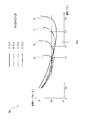
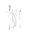
- the heating start temperature characteristic map is a state in which the nonconductive film is sandwiched between the bonding stage and the bonding tool and pressed with a constant load from the various heating start temperatures to the same temperature. While lowering the temperature of the nonconductive film at a rising rate, measure the descent amount of the bonding tool, calculate the viscosity of the nonconductive film based on the descent amount of the bonding tool, and start the heating start temperature at the same temperature rising rate. It may be output as a change characteristic of viscosity with respect to the temperature of the nonconductive film when changing.
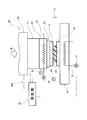
- the bonding apparatus 100 includes a bonding stage 10 for vacuum-sucking the semiconductor chip 32 on the surface, a bonding tool 24 for vacuum-sucking the semiconductor chip 31, a bonding head 20, and a control unit 90.
- the bonding head 20 includes a base 21, a heat block 22 attached to the base 21, and a drive unit 25 for driving the base 21 in the vertical direction.
- the bonding tool 24 is fixed to the heat block 22 by vacuum suction.
- the bonding stage 10 incorporates a heater 12 for heating the semiconductor chip 32, and the heat block 22 incorporates a heater 23 for heating the semiconductor chip 31. Connected to the heaters 12 and 23 are controllers 14 and 26 for adjusting the power supplied to the heaters 12 and 23, respectively.
- the control unit 90 is a computer that internally includes a CPU and a memory.
- the drive unit 25 of the bonding head 20 drives the bonding tool 24 in the vertical direction based on the command of the control unit 90, and outputs the height of the bonding tool 24 and the pressing load F of the bonding tool 24 to the control unit 90.
- the heat block 22 is attached with a temperature sensor 91 for detecting the temperature of the heat block 22. Further, a temperature sensor 92 for detecting the temperature of the NCF 40 is attached to the bonding apparatus 100.
- the temperature sensor 92 may be, for example, a non-contact temperature sensor. The temperature data acquired by the temperature sensors 91 and 92 is input to the control unit 90.
Landscapes
- Wire Bonding (AREA)
Abstract
Description
V=2*π*F*H5/3*Q*(-dH/dt)(2*π*H3+Q) ---- (式1)
Claims (9)
- 非導電性フィルムを用いて半導体チップをボンディングする際の半導体チップの加熱条件設定方法であって、
各種の温度上昇率における非導電性フィルムの温度に対する粘度の変化を示す粘度特性マップと、同一の温度上昇率で加熱開始温度を変化させた場合の非導電性フィルムの温度に対する粘度の変化を示す加熱開始温度特性マップと、のいずれか一方または両方に基づいて加熱開始温度と温度上昇率とを設定すること、
を特徴とする加熱条件設定方法。 - 請求項1に記載の加熱条件設定方法であって、
ボンディングは、半導体チップに形成された金属バンプを溶融させて基板あるいは他の半導体チップの電極との間で合金を形成することにより半導体チップを基板または他の半導体チップに接合し、非導電性フィルムを熱硬化させて半導体チップと基板あるいは他の半導体チップとの間の隙間を充填するものであり、
加熱開始温度と温度上昇率の設定は、金属バンプの溶融開始温度よりも低い温度で非導電性フィルムの粘度が硬化粘度以上となる加熱開始温度と温度上昇率の組み合わせを選択すること、
を特徴とする加熱条件設定方法。 - 請求項1または2に記載の加熱条件設定方法であって、
粘度特性マップは、
ボンディングステージとボンディングツールの間に非導電性フィルムを挟みこんで一定の荷重で押圧した状態で、各種の温度上昇率で非導電性フィルムの温度を上昇させながら、ボンディングツールの降下量を測定し、ボンディングツールの降下量に基づいて非導電性フィルムの粘度を算出し、各種の温度上昇率における非導電性フィルムの温度に対する粘度の変化特性として出力したものである加熱条件設定方法。 - 請求項1または2に記載の加熱条件設定方法であって、
加熱開始温度特性マップは、
ボンディングステージとボンディングツールの間に非導電性フィルムを挟みこんで一定の荷重で押圧した状態で、各種の加熱開始温度から同一の温度上昇率で非導電性フィルムの温度を上昇させながら、ボンディングツールの降下量を測定し、ボンディングツールの降下量に基づいて非導電性フィルムの粘度を算出し、同一の温度上昇率で加熱開始温度を変化させた場合の非導電性フィルムの温度に対する粘度の変化特性として出力したものである加熱条件設定方法。 - 請求項1または2に記載の加熱条件設定方法であって、
設定した加熱開始温度と温度上昇率とに基づいて、半導体チップを加熱するヒータへの温度指令を設定する加熱条件設定方法。 - 請求項3に記載の加熱条件設定方法であって、
設定した加熱開始温度と温度上昇率とに基づいて、半導体チップを加熱するヒータへの温度指令を設定する加熱条件設定方法。 - 請求項4に記載の加熱条件設定方法であって、
設定した加熱開始温度と温度上昇率とに基づいて、半導体チップを加熱するヒータへの温度指令を設定する加熱条件設定方法。 - ボンディング装置を用いた非導電性フィルムの粘度測定方法であって、
ボンディングステージとボンディングツールの間に非導電性フィルムを挟みこんで一定の荷重で押圧した状態で、所定の温度上昇率で非導電性フィルムの温度を上昇させながら、ボンディングツールの降下量を測定し、
ボンディングツールの降下量に基づいて非導電性フィルムの粘度を算出する非導電性フィルムの粘度測定方法。 - ボンディング装置であって、
非導電性フィルムが載置されるボンディングステージと、
前記ボンディングステージと共に前記非導電性フィルムを挟み込むボンディングツールと、
前記ボンディングツールを上下方向に駆動するボンディングヘッドと、
前記ボンディングヘッドに内蔵されたヒータと、
前記ボンディングヘッドの高さと前記ヒータの出力とを調整する制御部と、を備え、
前記制御部は、
前記ボンディングヘッドを降下させて前記非導電性フィルムを一定の荷重で押圧した状態で、前記ヒータによって所定の温度上昇率で前記非導電性フィルムの温度を上昇させながら、前記ボンディングツールの降下量を測定し、
前記ボンディングツールの降下量に基づいて前記非導電性フィルムの粘度を算出すること、
を特徴とするボンディング装置。
Priority Applications (5)
| Application Number | Priority Date | Filing Date | Title |
|---|---|---|---|
| JP2019544590A JP7008348B2 (ja) | 2017-09-28 | 2018-09-14 | ボンディングの際の半導体チップの加熱条件設定方法及び非導電性フィルムの粘度測定方法ならびにボンディング装置 |
| KR1020207011353A KR102353013B1 (ko) | 2017-09-28 | 2018-09-14 | 본딩시의 반도체 칩의 가열 조건 설정 방법, 비도전성 필름의 점도 측정 방법 및 본딩 장치 |
| US16/651,334 US11201132B2 (en) | 2017-09-28 | 2018-09-14 | Method for setting conditions for heating semiconductor chip during bonding, method for measuring viscosity of non-conductive film, and bonding apparatus |
| SG11202003747YA SG11202003747YA (en) | 2017-09-28 | 2018-09-14 | Method for setting conditions for heating semiconductor chip during bonding, method for measuring viscosity of non-conductive film, and bonding device |
| CN201880062410.5A CN111149195A (zh) | 2017-09-28 | 2018-09-14 | 接合时的半导体晶片的加热条件设定方法以及非导电性膜的粘度测量方法以及接合装置 |
Applications Claiming Priority (2)
| Application Number | Priority Date | Filing Date | Title |
|---|---|---|---|
| JP2017187921 | 2017-09-28 | ||
| JP2017-187921 | 2017-09-28 |
Publications (1)
| Publication Number | Publication Date |
|---|---|
| WO2019065309A1 true WO2019065309A1 (ja) | 2019-04-04 |
Family
ID=65901291
Family Applications (1)
| Application Number | Title | Priority Date | Filing Date |
|---|---|---|---|
| PCT/JP2018/034203 Ceased WO2019065309A1 (ja) | 2017-09-28 | 2018-09-14 | ボンディングの際の半導体チップの加熱条件設定方法及び非導電性フィルムの粘度測定方法ならびにボンディング装置 |
Country Status (7)
| Country | Link |
|---|---|
| US (1) | US11201132B2 (ja) |
| JP (1) | JP7008348B2 (ja) |
| KR (1) | KR102353013B1 (ja) |
| CN (1) | CN111149195A (ja) |
| SG (1) | SG11202003747YA (ja) |
| TW (1) | TWI705120B (ja) |
| WO (1) | WO2019065309A1 (ja) |
Cited By (1)
| Publication number | Priority date | Publication date | Assignee | Title |
|---|---|---|---|---|
| JP2020149995A (ja) * | 2019-03-11 | 2020-09-17 | 株式会社新川 | 接合材料の化学的特性を抽出する装置 |
Families Citing this family (2)
| Publication number | Priority date | Publication date | Assignee | Title |
|---|---|---|---|---|
| JP2020119983A (ja) * | 2019-01-23 | 2020-08-06 | トヨタ自動車株式会社 | 半導体素子接合装置、及び半導体素子接合方法 |
| JP7287647B2 (ja) * | 2019-03-05 | 2023-06-06 | 株式会社新川 | 接合条件評価装置 |
Citations (2)
| Publication number | Priority date | Publication date | Assignee | Title |
|---|---|---|---|---|
| JP2015056500A (ja) * | 2013-09-11 | 2015-03-23 | デクセリアルズ株式会社 | アンダーフィル材、及びこれを用いた半導体装置の製造方法 |
| WO2016056619A1 (ja) * | 2014-10-10 | 2016-04-14 | ナミックス株式会社 | 熱硬化性樹脂組成物及びその製造方法 |
Family Cites Families (5)
| Publication number | Priority date | Publication date | Assignee | Title |
|---|---|---|---|---|
| JP2008145273A (ja) | 2006-12-11 | 2008-06-26 | Fujitsu Ltd | 樹脂粘度測定装置及び樹脂粘度測定方法 |
| KR102217826B1 (ko) * | 2013-11-26 | 2021-02-18 | 토레이 엔지니어링 컴퍼니, 리미티드 | 실장 장치 및 실장 방법 |
| CN105849879A (zh) * | 2013-12-26 | 2016-08-10 | 日东电工株式会社 | 半导体装置的制造方法和热固性树脂片 |
| JP2014237843A (ja) * | 2014-08-08 | 2014-12-18 | 日立化成株式会社 | フィルム状接着剤およびこれを用いた半導体装置の製造方法 |
| JP6438340B2 (ja) * | 2015-04-08 | 2018-12-12 | 積水化学工業株式会社 | 半導体接合用接着フィルム及び半導体装置の製造方法 |
-
2018
- 2018-09-14 WO PCT/JP2018/034203 patent/WO2019065309A1/ja not_active Ceased
- 2018-09-14 JP JP2019544590A patent/JP7008348B2/ja active Active
- 2018-09-14 SG SG11202003747YA patent/SG11202003747YA/en unknown
- 2018-09-14 KR KR1020207011353A patent/KR102353013B1/ko active Active
- 2018-09-14 CN CN201880062410.5A patent/CN111149195A/zh active Pending
- 2018-09-14 US US16/651,334 patent/US11201132B2/en active Active
- 2018-09-26 TW TW107133700A patent/TWI705120B/zh active
Patent Citations (2)
| Publication number | Priority date | Publication date | Assignee | Title |
|---|---|---|---|---|
| JP2015056500A (ja) * | 2013-09-11 | 2015-03-23 | デクセリアルズ株式会社 | アンダーフィル材、及びこれを用いた半導体装置の製造方法 |
| WO2016056619A1 (ja) * | 2014-10-10 | 2016-04-14 | ナミックス株式会社 | 熱硬化性樹脂組成物及びその製造方法 |
Cited By (2)
| Publication number | Priority date | Publication date | Assignee | Title |
|---|---|---|---|---|
| JP2020149995A (ja) * | 2019-03-11 | 2020-09-17 | 株式会社新川 | 接合材料の化学的特性を抽出する装置 |
| JP7253780B2 (ja) | 2019-03-11 | 2023-04-07 | 株式会社新川 | 接合材料の化学的特性を抽出する装置 |
Also Published As
| Publication number | Publication date |
|---|---|
| US20200286854A1 (en) | 2020-09-10 |
| TWI705120B (zh) | 2020-09-21 |
| KR102353013B1 (ko) | 2022-01-20 |
| KR20200059255A (ko) | 2020-05-28 |
| JPWO2019065309A1 (ja) | 2020-06-18 |
| CN111149195A (zh) | 2020-05-12 |
| TW201922996A (zh) | 2019-06-16 |
| US11201132B2 (en) | 2021-12-14 |
| JP7008348B2 (ja) | 2022-01-28 |
| SG11202003747YA (en) | 2020-05-28 |
Similar Documents
| Publication | Publication Date | Title |
|---|---|---|
| TWI648799B (zh) | 用於接合半導體元件的接合機的操作方法及接合機 | |
| CN102918936B (zh) | 电子器件安装装置及其方法 | |
| JP7008348B2 (ja) | ボンディングの際の半導体チップの加熱条件設定方法及び非導電性フィルムの粘度測定方法ならびにボンディング装置 | |
| CN110102925B (zh) | 一种金属与高分子焊接装置及焊接方法 | |
| CN100509236C (zh) | 控制电子组件装配装置中接触载荷的方法 | |
| US11069650B2 (en) | Bonding condition evaluation apparatus | |
| CN102151976A (zh) | 焊接设备 | |
| JP6594522B2 (ja) | 超音波溶着装置および超音波溶着方法 | |
| JP6057685B2 (ja) | パルスヒート方式のハンダ付け管理方法および管理装置 | |
| JPWO2015045997A1 (ja) | 実装装置および実装方法 | |
| JP5003590B2 (ja) | 電子部品の製造装置及びその製造方法 | |
| CN107293504A (zh) | 键合加热控制装置及其方法 | |
| JP2016143826A (ja) | 電力用半導体装置、超音波接合方法および超音波接合装置 | |
| KR20130141461A (ko) | 실장장치 및 실장방법 | |
| JP6277003B2 (ja) | ヒータチップ研磨工具 | |
| CN105158038B (zh) | 一种用于动态加载过程前样品升温的方法 | |
| JP7253780B2 (ja) | 接合材料の化学的特性を抽出する装置 | |
| Liu et al. | Ultrasonic Thick Wire Bonding Process Simulation and Validation for Silicon Carbide Power Devices | |
| TR2022020932A1 (tr) | Bi̇r arayüz sicakliği hesaplama yöntemi̇ | |
| JP2022175200A (ja) | 接合装置 | |
| Yu et al. | Sequential Reflow-Process Optimization to Reduce Die-Attach Solder Voids | |
| JP2005268432A (ja) | パワーモジュールの絶縁樹脂硬化方法および装置 | |
| JP2010056188A (ja) | 半田付け装置および半田付け方法 | |
| JP2014174719A (ja) | 電子部品の封止部材選定方法および電子部品の封止部材選定装置 |
Legal Events
| Date | Code | Title | Description |
|---|---|---|---|
| 121 | Ep: the epo has been informed by wipo that ep was designated in this application |
Ref document number: 18861630 Country of ref document: EP Kind code of ref document: A1 |
|
| ENP | Entry into the national phase |
Ref document number: 2019544590 Country of ref document: JP Kind code of ref document: A |
|
| NENP | Non-entry into the national phase |
Ref country code: DE |
|
| ENP | Entry into the national phase |
Ref document number: 20207011353 Country of ref document: KR Kind code of ref document: A |
|
| 122 | Ep: pct application non-entry in european phase |
Ref document number: 18861630 Country of ref document: EP Kind code of ref document: A1 |