WO2019059189A1 - 半導体装置製造用接着フィルム、並びに、半導体装置及びその製造方法 - Google Patents
半導体装置製造用接着フィルム、並びに、半導体装置及びその製造方法 Download PDFInfo
- Publication number
- WO2019059189A1 WO2019059189A1 PCT/JP2018/034514 JP2018034514W WO2019059189A1 WO 2019059189 A1 WO2019059189 A1 WO 2019059189A1 JP 2018034514 W JP2018034514 W JP 2018034514W WO 2019059189 A1 WO2019059189 A1 WO 2019059189A1
- Authority
- WO
- WIPO (PCT)
- Prior art keywords
- adhesive
- film
- carrier film
- piece
- semiconductor chip
- Prior art date
- Legal status (The legal status is an assumption and is not a legal conclusion. Google has not performed a legal analysis and makes no representation as to the accuracy of the status listed.)
- Ceased
Links
Images



Classifications
-
- H—ELECTRICITY
- H10—SEMICONDUCTOR DEVICES; ELECTRIC SOLID-STATE DEVICES NOT OTHERWISE PROVIDED FOR
- H10P—GENERIC PROCESSES OR APPARATUS FOR THE MANUFACTURE OR TREATMENT OF DEVICES COVERED BY CLASS H10
- H10P72/00—Handling or holding of wafers, substrates or devices during manufacture or treatment thereof
- H10P72/70—Handling or holding of wafers, substrates or devices during manufacture or treatment thereof for supporting or gripping
- H10P72/74—Handling or holding of wafers, substrates or devices during manufacture or treatment thereof for supporting or gripping using temporarily an auxiliary support
- H10P72/7402—Wafer tapes, e.g. grinding or dicing support tapes
-
- B—PERFORMING OPERATIONS; TRANSPORTING
- B32—LAYERED PRODUCTS
- B32B—LAYERED PRODUCTS, i.e. PRODUCTS BUILT-UP OF STRATA OF FLAT OR NON-FLAT, e.g. CELLULAR OR HONEYCOMB, FORM
- B32B27/00—Layered products comprising a layer of synthetic resin
-
- B—PERFORMING OPERATIONS; TRANSPORTING
- B32—LAYERED PRODUCTS
- B32B—LAYERED PRODUCTS, i.e. PRODUCTS BUILT-UP OF STRATA OF FLAT OR NON-FLAT, e.g. CELLULAR OR HONEYCOMB, FORM
- B32B37/00—Methods or apparatus for laminating, e.g. by curing or by ultrasonic bonding
- B32B37/12—Methods or apparatus for laminating, e.g. by curing or by ultrasonic bonding characterised by using adhesives
-
- B—PERFORMING OPERATIONS; TRANSPORTING
- B32—LAYERED PRODUCTS
- B32B—LAYERED PRODUCTS, i.e. PRODUCTS BUILT-UP OF STRATA OF FLAT OR NON-FLAT, e.g. CELLULAR OR HONEYCOMB, FORM
- B32B7/00—Layered products characterised by the relation between layers; Layered products characterised by the relative orientation of features between layers, or by the relative values of a measurable parameter between layers, i.e. products comprising layers having different physical, chemical or physicochemical properties; Layered products characterised by the interconnection of layers
- B32B7/02—Physical, chemical or physicochemical properties
-
- B—PERFORMING OPERATIONS; TRANSPORTING
- B32—LAYERED PRODUCTS
- B32B—LAYERED PRODUCTS, i.e. PRODUCTS BUILT-UP OF STRATA OF FLAT OR NON-FLAT, e.g. CELLULAR OR HONEYCOMB, FORM
- B32B7/00—Layered products characterised by the relation between layers; Layered products characterised by the relative orientation of features between layers, or by the relative values of a measurable parameter between layers, i.e. products comprising layers having different physical, chemical or physicochemical properties; Layered products characterised by the interconnection of layers
- B32B7/04—Interconnection of layers
- B32B7/12—Interconnection of layers using interposed adhesives or interposed materials with bonding properties
-
- B—PERFORMING OPERATIONS; TRANSPORTING
- B32—LAYERED PRODUCTS
- B32B—LAYERED PRODUCTS, i.e. PRODUCTS BUILT-UP OF STRATA OF FLAT OR NON-FLAT, e.g. CELLULAR OR HONEYCOMB, FORM
- B32B7/00—Layered products characterised by the relation between layers; Layered products characterised by the relative orientation of features between layers, or by the relative values of a measurable parameter between layers, i.e. products comprising layers having different physical, chemical or physicochemical properties; Layered products characterised by the interconnection of layers
- B32B7/04—Interconnection of layers
- B32B7/12—Interconnection of layers using interposed adhesives or interposed materials with bonding properties
- B32B7/14—Interconnection of layers using interposed adhesives or interposed materials with bonding properties applied in spaced arrangements, e.g. in stripes
-
- C—CHEMISTRY; METALLURGY
- C09—DYES; PAINTS; POLISHES; NATURAL RESINS; ADHESIVES; COMPOSITIONS NOT OTHERWISE PROVIDED FOR; APPLICATIONS OF MATERIALS NOT OTHERWISE PROVIDED FOR
- C09J—ADHESIVES; NON-MECHANICAL ASPECTS OF ADHESIVE PROCESSES IN GENERAL; ADHESIVE PROCESSES NOT PROVIDED FOR ELSEWHERE; USE OF MATERIALS AS ADHESIVES
- C09J7/00—Adhesives in the form of films or foils
-
- C—CHEMISTRY; METALLURGY
- C09—DYES; PAINTS; POLISHES; NATURAL RESINS; ADHESIVES; COMPOSITIONS NOT OTHERWISE PROVIDED FOR; APPLICATIONS OF MATERIALS NOT OTHERWISE PROVIDED FOR
- C09J—ADHESIVES; NON-MECHANICAL ASPECTS OF ADHESIVE PROCESSES IN GENERAL; ADHESIVE PROCESSES NOT PROVIDED FOR ELSEWHERE; USE OF MATERIALS AS ADHESIVES
- C09J7/00—Adhesives in the form of films or foils
- C09J7/20—Adhesives in the form of films or foils characterised by their carriers
- C09J7/22—Plastics; Metallised plastics
-
- H—ELECTRICITY
- H10—SEMICONDUCTOR DEVICES; ELECTRIC SOLID-STATE DEVICES NOT OTHERWISE PROVIDED FOR
- H10P—GENERIC PROCESSES OR APPARATUS FOR THE MANUFACTURE OR TREATMENT OF DEVICES COVERED BY CLASS H10
- H10P72/00—Handling or holding of wafers, substrates or devices during manufacture or treatment thereof
- H10P72/70—Handling or holding of wafers, substrates or devices during manufacture or treatment thereof for supporting or gripping
-
- H—ELECTRICITY
- H10—SEMICONDUCTOR DEVICES; ELECTRIC SOLID-STATE DEVICES NOT OTHERWISE PROVIDED FOR
- H10W—GENERIC PACKAGES, INTERCONNECTIONS, CONNECTORS OR OTHER CONSTRUCTIONAL DETAILS OF DEVICES COVERED BY CLASS H10
- H10W72/00—Interconnections or connectors in packages
- H10W72/071—Connecting or disconnecting
-
- C—CHEMISTRY; METALLURGY
- C09—DYES; PAINTS; POLISHES; NATURAL RESINS; ADHESIVES; COMPOSITIONS NOT OTHERWISE PROVIDED FOR; APPLICATIONS OF MATERIALS NOT OTHERWISE PROVIDED FOR
- C09J—ADHESIVES; NON-MECHANICAL ASPECTS OF ADHESIVE PROCESSES IN GENERAL; ADHESIVE PROCESSES NOT PROVIDED FOR ELSEWHERE; USE OF MATERIALS AS ADHESIVES
- C09J2203/00—Applications of adhesives in processes or use of adhesives in the form of films or foils
- C09J2203/326—Applications of adhesives in processes or use of adhesives in the form of films or foils for bonding electronic components such as wafers, chips or semiconductors
-
- C—CHEMISTRY; METALLURGY
- C09—DYES; PAINTS; POLISHES; NATURAL RESINS; ADHESIVES; COMPOSITIONS NOT OTHERWISE PROVIDED FOR; APPLICATIONS OF MATERIALS NOT OTHERWISE PROVIDED FOR
- C09J—ADHESIVES; NON-MECHANICAL ASPECTS OF ADHESIVE PROCESSES IN GENERAL; ADHESIVE PROCESSES NOT PROVIDED FOR ELSEWHERE; USE OF MATERIALS AS ADHESIVES
- C09J2301/00—Additional features of adhesives in the form of films or foils
- C09J2301/30—Additional features of adhesives in the form of films or foils characterized by the chemical, physicochemical or physical properties of the adhesive or the carrier
- C09J2301/312—Additional features of adhesives in the form of films or foils characterized by the chemical, physicochemical or physical properties of the adhesive or the carrier parameters being the characterizing feature
Definitions
- the present disclosure relates to an adhesive film used in a process of manufacturing a semiconductor device, and a semiconductor device and a method of manufacturing the same.
- Patent Document 1 discloses an adhesive sheet (dicing die bonding sheet) having a function of fixing a semiconductor wafer in a dicing step and a function of bonding a semiconductor chip to a substrate in a die bonding step.
- the shape of the semiconductor chip and the shape of the adhesive for bonding the same to the substrate are generally the same.
- these shapes are rectangular or square.
- the area of the substrate to which the semiconductor chip is to be bonded is limited, or when the electrical connection between the semiconductor chip and the substrate is required at a position different from the conventional one, in comparison with the conventional shape.
- An adhesive film for manufacturing a semiconductor device includes: a belt-like carrier film having a width of 100 mm or less; and a plurality of adhesive pieces arranged on the carrier film in the longitudinal direction of the carrier film
- the piece has a shape in which at least one of a protrusion and a recess is formed on at least one side of a rectangle or a square.
- a plurality of adhesive pieces arranged to be aligned on the carrier film can be sequentially picked up, and then each adhesive piece can be arranged in a predetermined area of the substrate, and the substrate and the semiconductor chip Can be carried out efficiently.
- the adhesive strip has a more complex shape than a rectangular or square, as described above.
- the shape of the adhesive piece may be appropriately set according to the shape of the region of the substrate to which the semiconductor chip is to be bonded or the shape of the semiconductor chip.
- the adhesive strip may have six or more corners, or eight or more corners.
- L-shaped is mentioned as an example of the shape of the adhesive agent piece which has six corners.
- the size and the number of adhesive pieces disposed on the carrier film may be appropriately set according to the design of the semiconductor device to be manufactured.
- the area of one adhesive strip can range from 10 to 200 mm 2 .
- the percentage of the area of the surface of the carrier film covered by the plurality of adhesive pieces can be 10 to 60% based on the area of the carrier film.
- An array of one or more adhesive strips may be formed on the carrier film.
- the plurality of adhesive strips can be formed, for example, by stamping an adhesive layer formed to cover the surface of the carrier film.
- the adhesion between the carrier film and the adhesive piece is It is preferably 0.5 to 18 N / m.
- the adhesive film according to the present disclosure covers the second surface opposite to the first surface on the carrier film side of the adhesive strip, and may further include a protective member having the same shape as the adhesive strip. By covering the adhesive strip with the protective member, dust and the like can be prevented from adhering to the adhesive strip until the time of use.
- the adhesive strip and the protective member can be formed by die cutting an adhesive layer formed to cover the surface of the carrier film and a protective film disposed to cover the adhesive layer.
- the light transmittance of the protective member is preferably lower than the light transmittance of the carrier film.
- the adhesion between the adhesive piece and the protective member is preferably 16 N / m or less.
- the adhesion between the adhesive strip and the protective member is preferably 16 N / m or less after heat treatment at 100 ° C. for 10 minutes. .
- an adhesive film provided with an adhesive strip of a complicated shape that is useful for efficiently performing the bonding process in the process of manufacturing a semiconductor device. Also, according to the present disclosure, a semiconductor device using a complex-shaped adhesive piece and a method of manufacturing the same are provided.
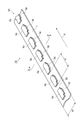
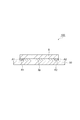
- FIG. 1 is a perspective view schematically showing an embodiment of an adhesive film according to the present disclosure.
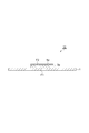
- FIG. 2 is a cross-sectional view taken along the line II-II shown in FIG. 3 (a) to 3 (f) are plan views showing variations of the shape of the adhesive piece.
- FIG. 4 is a plan view showing an example of the arrangement of T-shaped adhesive pieces and semiconductor chips.
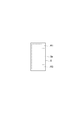
- FIG. 5: is sectional drawing which shows typically the laminated body on which the carrier film, the adhesive bond layer, and the protective film were laminated
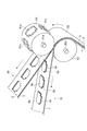
- FIG. 6 is a perspective view showing how a plurality of adhesive pieces are formed on the carrier film by die cutting.
- FIG. 7 is a cross-sectional view schematically showing how the adhesive strip and the protective member covering the adhesive strip are picked up from the carrier film.
- FIG. 8 is a cross-sectional view schematically showing an example of a semiconductor device manufactured using the adhesive strip according to the present disclosure.
- (meth) acrylic means acrylic or methacrylic.
- FIG. 1 is a perspective view schematically showing an adhesive film according to the present embodiment.
- FIG. 2 is a cross-sectional view taken along the line II-II shown in FIG.
- Adhesive films 10 shown in these figures are a band-like carrier film 1 having a width of 100 mm or less, and a plurality of carrier films 1 arranged on the carrier film 1 in the longitudinal direction (direction of arrow X shown in FIG. 1).
- the adhesive strip 3p and the protective member 5p covering the surface F2 of the adhesive strip 3p and having the same shape as the adhesive strip 3p are provided.
- the surface F2 (second surface) of the adhesive piece 3p is a surface opposite to the surface F1 (first surface) of the adhesive piece 3p on the carrier film 1 side.
- the adhesive film 10 is applicable to various adhesion processes (for example, adhesion of a semiconductor chip and a substrate) in a manufacturing process of a semiconductor device.
- a plurality of adhesive pieces 3p arranged to line up on the carrier film 1 can be sequentially picked up, and then each adhesive piece 3p can be arranged in a predetermined area of the substrate, and the substrate
- the step of bonding the semiconductor chip to the semiconductor chip can be carried out efficiently.
- FIGS. 1 and 2 show the case where one row 3A of a plurality of adhesive pieces 3p is provided on the carrier film 1, two or more rows 3A are provided on the carrier film 1. It may be done.
- the adhesive agent piece 3p which concerns on this embodiment has a shape (T character shape) like a thick T character, as shown in FIG.
- This shape has eight angles C1 to C8, as shown in FIG. 3 (a).
- this shape can be said to be a shape in which one convex portion is formed at the central part of one side of a rectangle, and it can also be said to be a shape in which one recess is formed at each end of one side of a rectangle. .
- the shape of the adhesive piece 3p is not limited to the shape shown in FIG. 3A, and may be a shape in which at least one of a convex portion and a concave portion is formed on at least one side of a rectangle or a square.
- it may be L-shaped, and may have six corners C1 to C6.
- FIG. 3C it may have a shape in which one recess is formed in a rectangle or a square, and may have eight corners C1 to C8.
- a recess is formed at one corner (lower left in FIG. 3D) of a rectangle or square and a protrusion is formed on one side (right side in FIG. 3D).
- a convex portion is formed on one side of a rectangle or a square, and a concave portion is formed on the other side, and has twelve corners C1 to C12. It is also good.
- the shape of a recessed part or a convex part may be a triangle or circular arc shape, as shown to FIG. 3 (f).
- the shape of the adhesive piece may be appropriately set according to the shape of the region of the substrate to which the semiconductor chip is to be bonded or the shape of the semiconductor chip.
- the semiconductor chip has, for example, a rectangular or square shape and a plurality of terminals are provided at the corners, and it is necessary to connect these terminals to the wiring of the substrate, the terminals and the wiring are adhesive
- the shape of the adhesive strip may be determined so as not to be covered by the strip.
- FIG. 4 is a plan view showing an example of the arrangement of the T-shaped adhesive piece 3p and the rectangular semiconductor chip S. As shown in FIG. In the regions R1 and R2 shown in FIG. 4, no adhesive is present between the substrate and the semiconductor chip, and the substrate and the semiconductor chip can be electrically connected in these regions R1 and R2.
- the adhesive strip 3p in this embodiment is assumed to have a sufficiently small size, and the area of one adhesive strip 3p is, for example, 10 to 200 mm 2 , 20 to 160 mm 2 or 25 to 100 mm 2 . It may be.
- the ratio of the area (area ratio of adhesive pieces) on the surface of the carrier film 1 and covered by the plurality of adhesive pieces 3p is, for example, 10 to 60% based on the area of the carrier film 1; It may be 10 to 35% or 15 to 33%.
- the carrier film 1 is band-like and has a width of 100 mm or less.
- the width of the carrier film 1 may be appropriately set in accordance with the size of the adhesive piece 3p disposed thereon and the number of rows 3A.
- the width of the carrier film 1 is preferably 10 to 50 mm, and may be 10 to 30 mm or 10 to 20 mm.
- the width of the carrier film 1 is 10 mm or more, when the roll-to-roll method is adopted, it is easy to prevent the deterioration in workability caused by the twisting of the carrier film 1.
- the material of the carrier film 1 is not particularly limited as long as it can sufficiently withstand the tension applied in the manufacturing process of the adhesive film 10 and the manufacturing process of the semiconductor device.
- the carrier film 1 is preferably transparent from the viewpoint of the visibility of the adhesive piece 3p and / or the protective member 5p disposed thereon.
- the carrier film 1 may be a polyester film such as polyethylene terephthalate film, polytetrafluoroethylene film, polyethylene film, polypropylene film, polymethylpentene film, polyvinyl acetate film, poly-4-methylpentene-1, ethylene-vinyl acetate co
- a polyolefin film such as a polymer, a homopolymer or copolymer such as ethylene-ethyl acrylate copolymer, or a mixture thereof, a plastic film such as a polyvinyl chloride film or a polyimide film, or the like can be used.
- the carrier film 1 may have a single layer structure or a multilayer structure.
- the thickness of the carrier film 1 may be appropriately selected within a range that does not impair the workability, and is, for example, 10 to 200 ⁇ m, and may be 20 to 100 ⁇ m or 25 to 80 ⁇ m. These thickness ranges are practically acceptable and economically effective.
- the carrier film 1 it is also possible to use a low surface energy film made of a fluorocarbon resin.
- a film for example, A-63 (release treatment agent: modified silicone type) manufactured by Teijin Film Solutions Ltd., and A-31 (release treatment agent: Pt type manufactured by Teijin Film Solutions Ltd.) There are silicone type etc.
- the surface of the carrier film 1 is separated from silicone release agent, fluorine release agent, long chain alkyl acrylate release agent, etc. You may form the release layer comprised from a mold agent.
- the adhesion between the carrier film 1 and the adhesive strip 3p is preferably 0.5 to 18 N / m, more preferably 2 to 10 N / m, 2 to 6 N / m or 2 to 4 N / m. It may be m.
- the adhesion is 0.5 N / m or more, careless peeling of the adhesive piece 3p from the carrier film 1 in the process of producing the adhesive film 10 can be easily prevented, and on the other hand, 18 N / m or less
- the adhesion of the adhesive strip 3p to the carrier film 1 means 90 ° peel strength.
- an adhesive layer of 20 mm in width made of the same composition as the adhesive strip 3p is formed on the carrier film 1
- the prepared sample is prepared, which means the peel strength measured when the adhesive layer is peeled from the carrier film at an angle of 90 ° and a peeling speed of 50 mm / min.
- the adhesive strip 3p is formed by simultaneously die-cutting the adhesive layer 3 formed to cover the surface of the carrier film 1 and the protective film 5 disposed to cover the adhesive layer 3 to form a protective member 5p. (See FIG. 6).
- the thickness of the adhesive piece 3p may be appropriately selected within a range that does not impair the workability, and is, for example, 3 to 50 ⁇ m, and may be 5 to 40 ⁇ m or 7 to 30 ⁇ m. Sufficient adhesion can be easily secured by the thickness of the adhesive strip 3p being 3 ⁇ m or more, and the adhesive composition constituting the adhesive strip 3p can be protruded from the protective member 5p by being 50 ⁇ m or less It is easy to control.
- the adhesive composition constituting the adhesive strip 3p only needs to have properties (for example, adhesiveness and heat resistance to heat of about 150 ° C.) that can be used without problems in the manufacturing process of the semiconductor device. What is used in the manufacturing process of the semiconductor device may be adopted appropriately.
- the adhesive strip 3p preferably contains a thermoplastic resin, a thermosetting resin, a curing accelerator, and a filler, and may contain a photoreactive monomer, a photopolymerization initiator, and the like as necessary. With the thinning of substrates, substrates having low heat resistance tend to be used, and there is a need to lower the temperature of the manufacturing process of semiconductor devices. It is preferable that the adhesive strip 3p can adhere an object under temperature conditions of 160 ° C. or less.
- thermoplastic resin a resin having thermoplasticity or a resin having thermoplasticity at least in an uncured state and forming a crosslinked structure after heating can be used.
- a thermoplastic resin as a tape for processing a semiconductor, a (meth) acrylic copolymer (hereinafter referred to as “reactive group-containing (meth) acrylic copolymer”) having a reactive group from the viewpoint of being excellent in shrinkage, heat resistance and peelability. It may be called "polymer”) is preferable.
- the adhesive piece 3p may not include the thermosetting resin. That is, the aspect containing a reactive group containing (meth) acrylic copolymer, a hardening accelerator, and a filler may be sufficient.
- a thermoplastic resin can be used individually by 1 type or in combination of 2 or more types.
- Examples of the (meth) acrylic copolymer include (meth) acrylic acid ester copolymers such as acrylic resin and acrylic rubber, and acrylic rubber is preferable.
- the acrylic rubber preferably comprises an acrylic ester as a main component and is formed by copolymerization of a monomer selected from (meth) acrylic ester and acrylonitrile.
- (meth) acrylic acid esters methyl acrylate, ethyl acrylate, propyl acrylate, isopropyl acrylate, butyl acrylate, isobutyl acrylate, hexyl acrylate, cyclohexyl acrylate, 2-ethylhexyl acrylate, lauryl acrylate, methyl methacrylate, ethyl methacrylate, propyl methacrylate, Examples thereof include isopropyl acrylate, butyl methacrylate, isobutyl methacrylate, hexyl methacrylate, cyclohexyl methacrylate, 2-ethylhexyl methacrylate, lauryl methacrylate and the like.
- (meth) acrylic acid ester copolymer a copolymer containing butyl acrylate and acrylonitrile as a copolymer component, and a copolymer containing ethyl acrylate and acrylonitrile as a copolymer component are preferable.
- the reactive group-containing (meth) acrylic copolymer is preferably a reactive group-containing (meth) acrylic copolymer containing a (meth) acrylic monomer having a reactive group as a copolymerization component.
- a reactive group-containing (meth) acrylic copolymer can be obtained by copolymerizing a monomer composition containing a (meth) acrylic monomer having a reactive group and the above-described monomer. .
- the reactive group is preferably an epoxy group, a carboxyl group, an acryloyl group, a methacryloyl group, a hydroxyl group or an episulfide group from the viewpoint of heat resistance improvement, and from the viewpoint of crosslinkability, an epoxy group and a carboxyl group are more preferable.
- the reactive group-containing (meth) acrylic copolymer is preferably an epoxy group-containing (meth) acrylic copolymer containing a (meth) acrylic monomer having an epoxy group as a copolymerization component.
- the (meth) acrylic monomer having an epoxy group glycidyl acrylate, 4-hydroxybutyl acrylate glycidyl ether, 3,4-epoxycyclohexyl methyl acrylate, glycidyl methacrylate, 4-hydroxybutyl methacrylate glycidyl ether, 3,4- Epoxy cyclohexyl methyl methacrylate and the like can be mentioned.
- the (meth) acrylic monomer having a reactive group is preferably glycidyl acrylate or glycidyl methacrylate from the viewpoint of heat resistance.
- the Tg of the thermoplastic resin is preferably ⁇ 50 ° C. to 50 ° C.
- the Tg of the thermoplastic resin is 50 ° C. or less, the flexibility of the adhesive piece 3 p can be easily secured.
- the unevenness is present when pasted to the adherend, it becomes easy to follow and has appropriate adhesiveness.
- the Tg of the thermoplastic resin is ⁇ 50 ° C. or higher, it is easy to suppress the flexibility of the adhesive piece 3 p from becoming too high, and excellent handleability, adhesiveness, and releasability can be achieved.
- the Tg of a thermoplastic resin is the midpoint glass transition temperature value obtained by differential scanning calorimetry (DSC). Specifically, the Tg of the thermoplastic resin is an intermediate value calculated by the method according to JIS K 7121: 1987, measuring the change in heat quantity under the conditions of a temperature rising rate of 10 ° C./min and a measuring temperature of -80 to 80 ° C. It is a point glass transition temperature.
- the weight average molecular weight of the thermoplastic resin is preferably 100,000 or more and 2,000,000 or less.
- the weight average molecular weight is 100,000 or more, heat resistance can be easily secured when used for temporary fixation.
- the weight average molecular weight of the thermoplastic resin is more preferably 500,000 or more and 2,000,000 or less, and still more preferably 1,000,000 or more and 2,000,000 or less.
- a weight average molecular weight is a polystyrene conversion value which used the calibration curve by standard polystyrene by the gel permeation chromatography method (GPC).
- the total content of these is 0.1 to 20% by mass based on the total amount of the copolymerization component.
- the content is preferably 0.5 to 15% by mass, and more preferably 1.0 to 10% by mass. If the content is within the above range, it is easy to achieve all of the flexibility, adhesiveness and releasability of the adhesive strip 3p to a higher level.
- the (meth) acrylic copolymer having a reactive group as described above one obtained by a polymerization method such as pearl polymerization or solution polymerization may be used.
- a polymerization method such as pearl polymerization or solution polymerization
- commercially available products such as HTR-860P-3CSP (trade name, manufactured by Nagase ChemteX Co., Ltd.) may be used.
- thermosetting resin Any thermosetting resin can be used without particular limitation as long as it can be cured by heat.
- thermosetting resin epoxy resin, acrylic resin, silicone resin, phenol resin, thermosetting polyimide resin, polyurethane resin, melamine resin, urea resin, etc. may be mentioned. These can be used singly or in combination of two or more.
- the epoxy resin is not particularly limited as long as it cures and has a heat-resistant function.
- a bifunctional epoxy resin such as bisphenol A epoxy, a novolac epoxy resin such as phenol novolac epoxy resin, and a cresol novolac epoxy resin can be used.
- the epoxy resin conventionally known ones such as polyfunctional epoxy resin, glycidyl amine type epoxy resin, heterocycle-containing epoxy resin, alicyclic epoxy resin and the like can be used.
- Examples of the phenol novolac epoxy resin include Epicoat 152, Epicoat 154 (all manufactured by Mitsubishi Chemical Co., Ltd.), EPPN-201 (manufactured by Nippon Kayaku Co., Ltd.), DEN-438 (manufactured by Dow Chemical Co.) and the like.
- o-cresol novolac type epoxy resin As o-cresol novolac type epoxy resin, YDCN-700-10 (manufactured by Nippon Steel & Sumikin Chemical Co., Ltd.), EOCN-102S, EOCN-103S, EOCN-104S, EOCN-1012, EOCN-1025, EOCN-1027 (all of them) Nippon Kayaku Co., Ltd., YDCN 701, YDCN 702, YDCN 703, YDCN 704 (all manufactured by Nippon Steel & Sumikin Chemical Co., Ltd.) and the like.
- Epon 1031S made by Mitsubishi Chemical Corporation
- araldite 0163 made by BASF Japan Ltd.
- Denacol EX-611, EX-614, EX-614B, EX-622, EX-512, EX-521 And EX-421, EX-411 and EX-321 all of which are manufactured by Nagase ChemteX Co., Ltd.
- an amine type epoxy resin Epicoat 604 (made by Mitsubishi Chemical Corporation), YH-434 (made by Nippon Steel & Sumikin Chemical Co., Ltd.), TETRAD-X, TETRAD-C (all are made by Mitsubishi Chemical Co., Ltd.), ELM-120 (both) And Sumitomo Chemical Co., Ltd.).
- heterocycle-containing epoxy resin examples include Araldite PT810 (manufactured by BASF Japan Ltd.), ERL 4234, ERL 4299, ERL 4221, and ERL 4206 (all manufactured by Union Carbide). These epoxy resins can be used singly or in combination of two or more.
- the epoxy resin curing agent which is a part of the thermosetting resin component
- a commonly used known resin can be used. Specifically, amines, polyamides, acid anhydrides, polysulfides, boron trifluoride, bisphenol A, bisphenol F, bisphenols having two or more phenolic hydroxyl groups in one molecule such as bisphenol S, phenol novolac resin And phenol resins such as bisphenol A novolac resin and cresol novolac resin.
- phenol resins such as phenol novolac resin, bisphenol A novolac resin, and cresol novolac resin are preferable from the viewpoint of being excellent in electrolytic corrosion resistance at the time of moisture absorption.
- the epoxy curing agent may be used simultaneously with the epoxy resin or may be used alone.
- Phenolite LF 4871, Phenolite TD-2090, Phenolite TD-2149, Phenolite VH-4150, Phenolite VH 4170 (all manufactured by DIC Corporation, trade names), H-1 (Meiwa) Made by Kasei Co., Ltd., trade name, Epicure MP402FPY, Epicure YL6065, Epicure YLH129B65, Mirex XL, Mirex XLC, Mirex XLC-LL, Mirex RN, Mirex RS, Mirex VR (all are manufactured by Mitsubishi Chemical Corporation, etc.), etc. It is preferable to use a material having the following structure.
- the content of the thermosetting resin in the adhesive piece 3p is preferably 10 to 500 parts by mass, more preferably 30 to 450 parts by mass, and still more preferably 50 to 400 parts by mass with respect to 100 parts by mass of the thermoplastic resin. It is easy to achieve the outstanding adhesiveness after thermosetting of adhesive piece 3p as content of a thermosetting resin is in a mentioned range.
- adhesive piece 3p contains the (meth) acrylic copolymer which has an epoxy group
- the hardening accelerator which promotes hardening of the epoxy group contained in the said acrylic copolymer.
- curing accelerators that promote curing of epoxy groups include phenolic curing agents, acid anhydride curing agents, amine curing agents, imidazole curing agents, imidazoline curing agents, triazine curing agents, and phosphine curing agents. It can be mentioned. Among these, from the viewpoint of rapid curing, heat resistance and releasability, an imidazole-based curing agent which can be expected to shorten the process time and improve the workability is preferable. These compounds can be used singly or in combination of two or more.
- the content of the curing accelerator in the adhesive strip 3p is preferably 0.01 to 50 parts by mass, more preferably 0.02 to 20 parts by mass, and more preferably 0.025 to 10 parts by mass with respect to 100 parts by mass of the thermoplastic resin. Parts are more preferred. It exists in the tendency which can fully suppress the fall of storage stability, improving the hardenability of adhesive agent piece 3p as content of a hardening accelerator is in the said range.
- the adhesive strip 3p preferably contains an inorganic filler.
- the inorganic filler include metal fillers such as silver powder, gold powder and copper powder, and nonmetallic inorganic fillers such as silica, alumina, boron nitride, titania, glass, iron oxide and ceramic.
- the inorganic filler can be selected according to the desired function.
- the inorganic filler preferably has an organic group on the surface.
- the surface of the inorganic filler is modified with an organic group, so that the dispersibility in an organic solvent when preparing a varnish for forming the adhesive strip 3p, and the high elastic modulus and the excellent peeling of the adhesive strip 3p It is easy to make
- the inorganic filler having an organic group on the surface can be obtained, for example, by mixing a silane coupling agent represented by the following formula (B-1) and an inorganic filler and stirring at a temperature of 30 ° C. or more. It can be confirmed by UV measurement, IR measurement, XPS measurement or the like that the surface of the inorganic filler has been modified by the organic group.
- X represents an organic group selected from the group consisting of phenyl group, glycidoxy group, acryloyl group, methacryloyl group, mercapto group, amino group, vinyl group, isocyanate group and methacryloxy group;
- Is an integer of 0 or 1 to 10.
- R 11 , R 12 and R 13 each independently represent an alkyl group having 1 to 10 carbon atoms.
- alkyl group having 1 to 10 carbon atoms examples include methyl group, ethyl group, propyl group, butyl group, pentyl group, hexyl group, heptyl group, octyl group, nonyl group, decyl group, isopropyl group and isobutyl group.
- the alkyl group having 1 to 10 carbon atoms is preferably a methyl group, an ethyl group and a pentyl group from the viewpoint of easy availability.
- X is preferably an amino group, a glycidoxy group, a mercapto group and an isocyanate group, and more preferably a glycidoxy group and a mercapto group.
- s in the formula (B-1) is preferably 0 to 5, and more preferably 0 to 4.
- trimethoxyphenylsilane dimethyldimethoxyphenylsilane, triethoxyphenylsilane, dimethoxymethylphenylsilane, vinyltrimethoxysilane, vinyltriethoxysilane, vinyltris (2-methoxyethoxy) silane, N- (2 -Aminoethyl) -3-aminopropylmethyldimethoxysilane, N- (2-aminoethyl) -3-aminopropyltrimethoxysilane, 3-aminopropyltriethoxysilane, 3-aminopropyltrimethoxysilane, 3-glycide Xylpropyltrimethoxysilane, 3-glycidoxypropylmethyldimethoxysilane, 2- (3,4-epoxycyclohexyl) ethyltrimethoxysilane, 3-isocyanatopropyltrie
- 3-aminopropyltriethoxysilane, 3-glycidoxypropyltrimethoxysilane, 3-isocyanatopropyltriethoxysilane, 3-mercaptopropyltrimethoxysilane are preferable, trimethoxyphenylsilane, 3-glycidoxy Propyltrimethoxysilane and 3-mercaptopropyltrimethoxysilane are more preferred.
- the silane coupling agent can be used singly or in combination of two or more.
- the content of the coupling agent is preferably 0.01 to 50 parts by mass, and 0.05 to 20 parts by mass, with respect to 100 parts by mass of the inorganic filler, from the viewpoint of achieving a balance between heat resistance and storage stability.
- the amount is more preferably 0.5 to 10 parts by mass from the viewpoint of heat resistance improvement.
- the content of the inorganic filler in the adhesive piece 3p is preferably 600 parts by mass or less, more preferably 500 parts by mass or less, and 400 parts by mass or less with respect to 100 parts by mass of the thermoplastic resin. More preferable.
- the lower limit of the content of the inorganic filler is not particularly limited, but is preferably 5 parts by mass or more, and more preferably 8 parts by mass or more with respect to 100 parts by mass of the thermoplastic resin.
- Adhesive piece 3 p may contain an organic filler.
- the organic filler include carbon, rubber fillers, silicone particles, polyamide particles and polyimide particles. 300 mass parts or less are preferable with respect to 100 mass parts of thermoplastic resins, as for content of an organic filler, 200 mass parts or less are more preferable, and 100 mass parts or less are still more preferable.
- the lower limit of the content of the organic filler is not particularly limited, but is preferably 5 parts by mass or more with respect to 100 parts by mass of the thermoplastic resin.
- the adhesive strip 3p may be diluted with an organic solvent, if necessary.
- the organic solvent is not particularly limited, but can be determined in consideration of the volatility and the like at the time of film formation from the boiling point.
- relatively low boiling point solvents such as methanol, ethanol, 2-methoxyethanol, 2-ethoxyethanol, 2-butoxyethanol, methyl ethyl ketone, acetone, methyl isobutyl ketone, toluene, xylene, etc. It is preferable from the viewpoint of difficulty in curing.
- a solvent having a relatively high boiling point such as dimethylacetamide, dimethylformamide, N-methylpyrrolidone, cyclohexanone and the like. These solvents can be used singly or in combination of two or more.
- the protective member 5 p simultaneously cuts off the adhesive layer 3 formed so as to cover the surface of the carrier film 1 and the protective film 5 arranged so as to cover the adhesive layer 3 to form an adhesive piece 3 p. (See FIG. 6).
- the protective member 5p according to the present embodiment is formed at the same time as the adhesive piece 3p by die cutting, and thus has substantially the same shape as the adhesive piece 3p.
- the protective film 5 may be a film which can be punched out in the manufacturing process of the adhesive film 10 and can easily peel the protective member 5p from the adhesive piece 3p in the manufacturing process of the semiconductor device.
- the adhesion between the adhesive strip 3p and the protective member 5p is preferably 16 N / m or less, more preferably 10 N / m or less, and 5 N / m or less or 4.5 N / m or less It is also good.
- the adhesive strip 3p is made of a thermosetting resin composition, it is preferable that the adhesion of the protective member 5p to the adhesive strip 3p be in the above range after heat treatment at 100 ° C. for 10 minutes.
- the adhesion is 16 N / m or less, the adhesive strip 3p in a state of being covered with the protective member 5p is temporarily crimped to an adherend (for example, a substrate) under conditions of 100 ° C. for 3 seconds, for example.
- the adhesion of the protective member 5p to the adhesive strip 3p means 90 ° peel strength, and specifically, a protective film of the same width on a 20 mm wide adhesive layer made of the same composition as the adhesive strip 3p. Means a peel strength which is measured when the prepared sample is prepared and this protective film is peeled from the adhesive layer at an angle of 90 ° and a peeling speed of 300 mm / min.
- polyester-based films such as polyethylene terephthalate film, polytetrafluoroethylene film, polyethylene film, polypropylene film, polymethylpentene film, polyvinyl acetate film, poly-4-methylpentene-1, ethylene-vinyl acetate co
- a polyolefin film such as a polymer, a homopolymer or copolymer such as ethylene-ethyl acrylate copolymer, or a mixture thereof, a plastic film such as a polyvinyl chloride film or a polyimide film, or the like can be used.
- the protective film 5 may have a single layer structure or a multilayer structure.
- the thickness of the protective film 5 may be appropriately selected within a range that does not impair the workability, and is, for example, 10 to 200 ⁇ m, and may be 20 to 100 ⁇ m or 25 to 80 ⁇ m. These thickness ranges are practically acceptable and economically effective.
- the light transmittance of the protective member 5 p is preferably lower than the light transmittance of the carrier film 1.
- a device such as a camera
- the manufacturing method of the present embodiment includes the following steps.
- FIG. 5 is sectional drawing which shows typically the laminated body 20 prepared by (A) process.
- the laminate 20 can be produced as follows. First, the raw material resin composition of the adhesive layer 3 is dissolved in a solvent such as an organic solvent to prepare a varnished coating liquid. The coating liquid is applied onto the carrier film 1 and then the solvent is removed to form the adhesive layer 3.
- the coating method may, for example, be a knife coating method, a roll coating method, a spray coating method, a gravure coating method, a bar coating method or a curtain coating method. Next, the protective film 5 is attached to the surface of the adhesive layer 3 under the conditions of normal temperature to 60 ° C. Thereby, the laminated body 20 can be obtained.
- the laminated film is produced by bonding together the protective film 5 so that this may be covered, and this is cut
- FIG. 6 is a perspective view showing how a plurality of adhesive pieces 3p and a protective member 5p covering the adhesive pieces 3p are formed on the carrier film 1 by die cutting in the (B) step.
- the laminate 20 passes between the rotating body 51 having a plurality of blades 51 c for carrying out the die cutting on the outer peripheral surface and the roll 52 paired with the rotating body 51.
- An adhesive piece 3p and a protection member 5p according to the shape of the blade 51c are continuously formed on the carrier film 1.
- the surface on the protective film 5 side of the laminate 20 faces the rotating body 51
- the surface on the carrier film 1 side faces the roll 52.
- the depth of the cut formed in the laminate 20 by the blade 51c by adjusting the distance between the rotation shaft 51a of the rotating body 51 and the rotation shaft 52a of the roll 52 or changing the height of the blade 51c Can be adjusted.
- the laminate 20 which has passed between the rotating body 51 and the roll 52 is separated into the adhesive film 10 and the unnecessary portion 30 as shown in FIG. 6, and is wound around each reel (not shown).
- the unnecessary portion 30 includes the adhesive layer 3 and the protective film 5 in which the adhesive piece 3 p and the protective member 5 p are hollowed out.
- FIG. 7 is a cross-sectional view schematically showing how the adhesive strip 3p and the protective member 5p covering the adhesive strip 3p are picked up from the carrier film 1.
- the adhesive film 10 is moved in the direction of the arrow shown in FIG. 7 while bringing the surface of the adhesive film 10 on the carrier film 1 side into contact with the wedge shaped member 60 in a state where a constant tension is applied to the adhesive film 10.
- the front of the adhesive agent piece 3p and the protection member 5p will be in the state which floated from the carrier film 1.
- FIG. 7 is a cross-sectional view schematically showing how the adhesive strip 3p and the protective member 5p covering the adhesive strip 3p are picked up from the carrier film 1.
- the adhesive strip 3p and the protective member 5p are picked up by the pickup device 65 having a suction force.
- the pickup device 65 having a suction force.
- the adhesive strip 3p in a state of being covered by the protective member 5p is disposed at a predetermined position and direction of the substrate (not shown).
- temporary pressure bonding of the adhesive piece 3p to the substrate is performed.
- the temporary pressure bonding may be performed, for example, at a temperature of 60 to 150 ° C. and a pressing force of 0.05 to 1 MPa for 0.1 to 10 seconds.
- the adhesive piece 3p is in close contact with the substrate to such an extent that the adhesive piece 3p is weak but does not peel off the substrate.
- the protective member 5p is peeled off from the adhesive piece 3p using an adhesive tape or the like.
- the semiconductor chip After the semiconductor chip having a shape different from that of the adhesive piece 3p is disposed on the surface of the adhesive piece 3p exposed by the peeling of the protective member 5p, the semiconductor chip is crimped to the substrate.
- the pressure bonding may be performed, for example, at a temperature of 60 to 150 ° C. under a pressure of 0.05 to 1 MPa for 0.1 to 10 seconds.
- the heating temperature is desirably low, the pressure bonding temperature is preferably 160 ° C. or less, and the heat curing temperature thereafter is also preferably 160 ° C. or less.
- FIG. 8 is a cross-sectional view schematically showing an example of a semiconductor device manufactured using the adhesive piece 3p.
- the semiconductor device 100 shown in the figure is disposed between the semiconductor chip S, the substrate 50 to which the semiconductor chip S is electrically connected, and the semiconductor chip S and the substrate 50.
- the semiconductor chip S and the substrate 50 And an adhesive strip 3p for bonding the
- the shape of the semiconductor chip S is, for example, rectangular or square, while the shape of the adhesive piece 3p is T-shaped, and the shape of the semiconductor chip S is different from the shape of the adhesive piece 3p.
- the substrate 50 and the semiconductor chip S can be electrically connected by the conductive materials A1 and A2 in the regions R1 and R2.
- the method of manufacturing the semiconductor device 100 includes the steps of preparing a laminate (not shown) in which the substrate 50, the adhesive piece 3p, and the semiconductor chip S are laminated in this order, and heating the laminate. Bonding the substrate 50 and the semiconductor chip S via The temperature for bonding the substrate 50 and the semiconductor chip S is preferably a low temperature, for example, 160 ° C. or less.
- this indication is not limited to the above-mentioned embodiment.
- the case where the colored protective film 5 is used is illustrated so that the presence or absence, the direction, etc. of the protective member 5p can be grasped by a camera or the like, but instead of this, a predetermined protective member 5p is used. The position of may be marked.
- it is set as the aspect by which the adhesive agent piece 3p was colored it is not necessary to provide the protection member 5p.
- the direction of the adhesive piece 3p does not matter, it is not necessary to identify the direction.
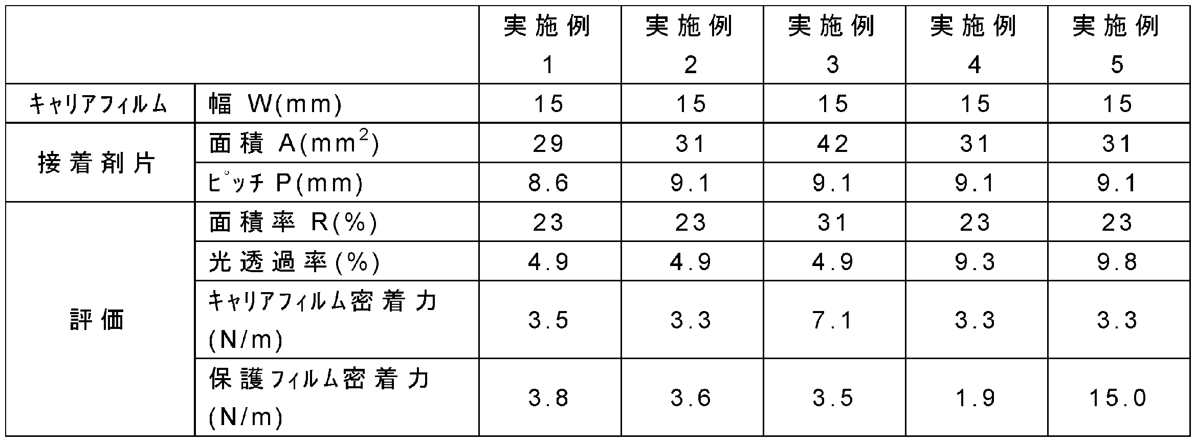
- Example 1 (Preparation of adhesive varnish) An adhesive varnish was obtained by mixing the following materials and vacuum degassing.
- Thermoplastic resin: HTR-860P-3 (trade name, manufactured by Nagase ChemteX Co., Ltd., glycidyl group-containing acrylic rubber, molecular weight 1,000,000, Tg-7 ° C.) 100 parts by mass
- Thermosetting resin: YDCN-700-10 (Trade name, manufactured by Nippon Steel & Sumikin Chemical Co., Ltd., o-cresol novolac epoxy resin, epoxy equivalent weight 210) 30 parts by mass
- Thermosetting resin: LF-4871 (trade name, manufactured by DIC, bisphenol A epoxy resin, Epoxy equivalent 118) 95 parts by mass
- Thermosetting resin: YDF-8170C (trade name, manufactured by Nippon Steel Sumikin Chemical Co., Ltd., bisphenol F type epoxy resin, epoxy equivalent 157) 100 parts by mass Curing accelerator: 2PZ-CN (com
- the adhesive varnish was coated on a surface release-treated polyethylene terephthalate film (manufactured by Teijin Film Solutions Co., Ltd., trade name: Teijin Tetron Film A-63) with a thickness of 50 ⁇ m. After the drying step, a film having a 25 ⁇ m-thick adhesive layer formed on one side of the polyethylene terephthalate film (carrier film) was obtained. A laminated film was obtained by laminating this film and a colored 50 ⁇ m-thick polyethylene film (manufactured by Tamapoly Co., Ltd., TDM-1). By slitting this laminated film to a width of 15 mm, a strip-like laminated body was obtained.
- the laminated film obtained as described above was die-cut by using an apparatus having a configuration shown in FIG. 6 to obtain an adhesive film according to this example.
- the shape of the adhesive piece was a shape (area: 29 mm 2 ) in which a corner of a part of a rectangle of about 7 mm in length ⁇ about 6 mm in width was missing.
- the pitch P was about 9 mm.
- the area ratio R of the adhesive piece was 23%.
- Example 2 An adhesive film was produced in the same manner as in Example 1 except that the size and pitch of the adhesive pieces were changed.
- Example 3 An adhesive film was produced in the same manner as in Example 2 except that a carrier film having a different surface treatment from that of the carrier film used in Example 2 was used and the shape of the adhesive piece was changed.
- a carrier film a surface release-treated polyethylene terephthalate film (manufactured by Teijin Film Solutions Co., Ltd., trade name: Teijin Tetron Film A-53) having a thickness of 50 ⁇ m was used.
- Example 4 An adhesive film was produced in the same manner as in Example 2 except that a protective film different from the protective film used in Example 2 was used.
- a protective film a non-colored polyethylene film (manufactured by Tamapoly Corporation, trade name: NF-13, thickness: 20 ⁇ m) was used.
- Example 5 An adhesive film was produced in the same manner as in Example 2 except that a protective film different from the protective film used in Example 2 was used.
- a protective film a non-colored polyethylene film (manufactured by Tamapoly Corporation, trade name: GF-3, thickness: 30 ⁇ m) was used.
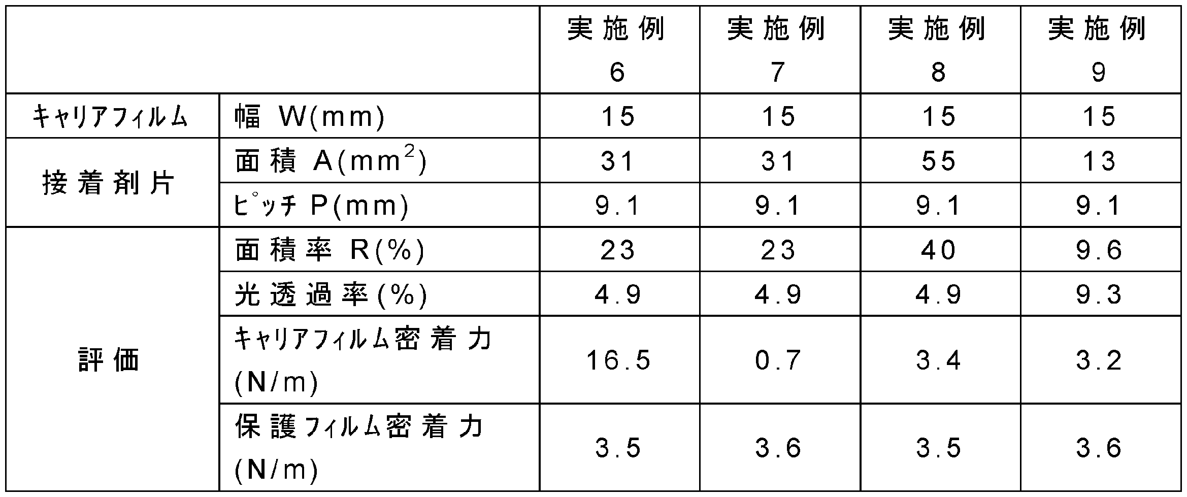
- Example 6 An adhesive film was produced in the same manner as in Example 2 except that a carrier film different from the carrier film used in Example 2 was used.
- a carrier film a polyethylene terephthalate film (manufactured by Teijin Film Solutions Co., Ltd., trade name: Teijin Tetron Film G2, thickness: 50 ⁇ m) not subjected to surface release treatment was used.
- Example 7 An adhesive film was produced in the same manner as in Example 2 except that a carrier film different from the carrier film used in Example 2 was used.
- a carrier film a polyethylene terephthalate film (manufactured by Teijin Film Solutions Co., Ltd., trade name: Teijin Tetron Film G2, thickness: 38 ⁇ m) not subjected to surface release treatment was used.
- Example 8 An adhesive film was produced in the same manner as in Example 2 except that the size of the adhesive strip was changed.
- Example 9 An adhesive film was produced in the same manner as in Example 2 except that the size of the adhesive strip was changed.
- Light Transmittance V-570 (trade name) manufactured by JASCO Corporation is used to transmit light with a wavelength of 500 nm in a region where an adhesive strip and a protective member covering the adhesive film are provided on a carrier film. Measured.
- Adhesion of protective film (90 ° peel strength)
- a laminated film (carrier film / adhesive layer / protective film) not cut was cut into a width of 20 mm.
- the protective film is upward while maintaining the angle of the protective film to the adhesive layer at 90 °.
- the adhesive layer was peeled off from the protective film by pulling up. The pulling rate was 300 mm / min, and the measurement environment temperature was 23 ⁇ 2 ° C. The force required to pull it up was measured.
- the adhesion between the protective film and the adhesive layer was calculated by substituting the measured value (mN) and the width (20 mm) of the sample into the following equation.
- Adhesion (N / m) measured value (mN) / 20 (mm)
- an adhesive film provided with an adhesive strip of a complicated shape that is useful for efficiently performing the bonding process in the process of manufacturing a semiconductor device. Also, according to the present disclosure, a semiconductor device using a complex-shaped adhesive piece and a method of manufacturing the same are provided.
Landscapes
- Chemical & Material Sciences (AREA)
- Organic Chemistry (AREA)
- Adhesive Tapes (AREA)
- Adhesives Or Adhesive Processes (AREA)
- Die Bonding (AREA)
- Laminated Bodies (AREA)
- Wire Bonding (AREA)
- Container, Conveyance, Adherence, Positioning, Of Wafer (AREA)
Abstract
Description
図1は本実施形態に係る接着フィルムを模式的に示す斜視図である。図2は図1に示すII-II線における断面図である。これらの図に示す接着フィルム10は、幅100mm以下の帯状のキャリアフィルム1と、キャリアフィルム1上に、その長手方向(図1に示す矢印Xの方向)に並ぶように配置されている複数の接着剤片3pと、接着剤片3pの表面F2を覆っており且つ接着剤片3pと同じ形状を有する保護部材5pとを備える。図2に示すとおり、接着剤片3pの表面F2(第二面)は、接着剤片3pのキャリアフィルム1側の面F1(第一面)と反対側の面である。
面積率R(%)=A/(P×W)×100
[キャリアフィルム]
キャリアフィルム1は、上述のとおり、帯状であって、100mm以下の幅を有する。キャリアフィルム1の幅は、その上に配置する接着剤片3pのサイズ及び列3Aの数に応じて適宜設定すればよい。例えば、図1に示すように、列3Aの数が一つである場合、キャリアフィルム1の幅は10~50mmであることが好ましく、10~30mm又は10~20mmであってもよい。キャリアフィルム1の幅が10mm以上であることで、ロールtoロール方式を採用した場合、キャリアフィルム1が捻れることに起因する作業性低下を防止しやすい。
接着剤片3pは、キャリアフィルム1の表面を覆うように形成された接着剤層3と、接着剤層3を覆うように配置された保護フィルム5とを同時に型抜きすることにより、保護部材5pとともに形成されるものである(図6参照)。接着剤片3pの厚さは、作業性を損なわない範囲で適宜選択すればよく、例えば、3~50μmであり、5~40μm又は7~30μmであってもよい。接着剤片3pの厚さが3μm以上であることで十分な接着性を確保しやすく、他方、50μm以下であることで接着剤片3pを構成する接着剤組成物が保護部材5pからはみ出ることを抑制しやすい。
熱可塑性樹脂としては、熱可塑性を有する樹脂、又は少なくとも未硬化状態において熱可塑性を有し、加熱後に架橋構造を形成する樹脂を用いることができる。熱可塑性樹脂としては、半導体加工用テープとして、収縮性、耐熱性及び剥離性に優れる観点から、反応性基を有する(メタ)アクリル共重合体(以下、「反応性基含有(メタ)アクリル共重合体」という場合もある)が好ましい。
熱可塑性樹脂として、反応性基含有(メタ)アクリル共重合体を含む場合、接着剤片3pは、熱硬化性樹脂を含まない態様でもよい。すなわち、反応性基含有(メタ)アクリル共重合体と、硬化促進剤と、フィラーとを含む態様でもよい。
熱可塑性樹脂は、一種を単独で又は二種以上を組み合わせて用いることができる。
(メタ)アクリル酸エステル共重合体としては、共重合成分としてブチルアクリレート及びアクリロニトリルを含む共重合体、共重合成分としてエチルアクリレート及びアクリロニトリルを含む共重合体が好ましい。
熱硬化性樹脂としては、熱により硬化する樹脂であれば特に制限なく用いることができる。熱硬化性樹脂としては、エポキシ樹脂、アクリル樹脂、シリコーン樹脂、フェノール樹脂、熱硬化型ポリイミド樹脂、ポリウレタン樹脂、メラミン樹脂、ユリア樹脂等が挙げられる。これらは、一種を単独で又は二種以上を組み合わせて用いることができる。
フェノールノボラック型エポキシ樹脂としては、エピコート152、エピコート154(いずれも三菱ケミカル株式会社製)、EPPN-201(日本化薬株式会社製)、DEN-438(ダウケミカル社製)等が挙げられる。
o-クレゾールノボラック型エポキシ樹脂としては、YDCN-700-10(新日鉄住金化学株式会社製)、EOCN-102S、EOCN-103S、EOCN-104S、EOCN-1012、EOCN-1025、EOCN-1027(いずれも日本化薬株式会社製)、YDCN701、YDCN702、YDCN703、YDCN704(いずれも新日鉄住金化学株式会社製)等が挙げられる。
多官能エポキシ樹脂としては、Epon 1031S(三菱ケミカル株式会社製)、アラルダイト0163(BASFジャパン社製)、デナコールEX-611、EX-614、EX-614B、EX-622、EX-512、EX-521、EX-421、EX-411、EX-321(いずれもナガセケムテックス株式会社製)等が挙げられる。
アミン型エポキシ樹脂としては、エピコート604(三菱ケミカル株式会社製)、YH-434(新日鉄住金化学株式会社製)、TETRAD-X、TETRAD-C(いずれも三菱ケミカル株式会社製)、ELM-120(住友化学株式会社製)等が挙げられる。
複素環含有エポキシ樹脂としては、アラルダイトPT810(BASFジャパン社製)、ERL4234、ERL4299、ERL4221、ERL4206(いずれもユニオンカーバイド社製)等が挙げられる。これらのエポキシ樹脂は、一種を単独で又は二種以上を組み合わせて用いることができる。
なお、エポキシ硬化剤は、エポキシ樹脂と同時に用いてもよいし、単独で用いてもよい。
硬化促進剤としては、イミダゾール類、ジシアンジアミド誘導体、ジカルボン酸ジヒドラジド、トリフェニルホスフィン、テトラフェニルホスホニウムテトラフェニルボレート、2-エチル-4-メチルイミダゾール-テトラフェニルボレート、1,8-ジアザビシクロ[5,4,0]ウンデセン-7-テトラフェニルボレート等が挙げられる。これらは、一種を単独で又は二種以上を組み合わせて用いることができる。
接着剤片3pは、無機フィラーを含有することが好ましい。無機フィラーとしては、銀粉、金粉、銅粉等の金属フィラー、シリカ、アルミナ、窒化ホウ素、チタニア、ガラス、酸化鉄、セラミック等の非金属無機フィラーなどが挙げられる。無機フィラーは所望する機能に応じて選択することができる。

炭素数1~10のアルキル基としては、メチル基、エチル基、プロピル基、ブチル基、ペンチル基、ヘキシル基、ヘプチル基、オクチル基、ノニル基、デシル基、イソプロピル基、イソブチル基等が挙げられる。
炭素数1~10のアルキル基は、入手が容易であるという観点から、メチル基、エチル基及びペンチル基が好ましい。Xは、耐熱性の観点から、アミノ基、グリシドキシ基、メルカプト基及びイソシアネート基が好ましく、グリシドキシ基及びメルカプト基がより好ましい。式(B-1)中のsは、高熱時のフィルム流動性を抑制し、耐熱性を向上させる観点から、0~5が好ましく、0~4がより好ましい。
これらの中でも、3-アミノプロピルトリエトキシシラン、3-グリシドキシプロピルトリメトキシシラン、3-イソシアネートプロピルトリエトキシシラン、3-メルカプトプロピルトリメトキシシランが好ましく、トリメトキシフェニルシラン、3-グリシドキシプロピルトリメトキシシラン、3-メルカプトプロピルトリメトキシシランがより好ましい。シランカップリング剤は、一種を単独で又は二種以上を組み合わせて用いることができる。
接着剤片3pは、有機フィラーを含有してもよい。有機フィラーとしては、カーボン、ゴム系フィラー、シリコーン系微粒子、ポリアミド微粒子、ポリイミド微粒子等が挙げられる。有機フィラーの含有量は、熱可塑性樹脂100質量部に対し、300質量部以下が好ましく、200質量部以下がより好ましく、100質量部以下が更により好ましい。有機フィラーの含有量の下限は特に制限はないが、熱可塑性樹脂100質量部に対し、5質量部以上であることが好ましい。
接着剤片3pは、必要に応じて、有機溶剤を用いて希釈してもよい。有機溶剤は特に限定されないが、製膜時の揮発性等を沸点から考慮して決めることができる。具体的には、メタノール、エタノール、2-メトキシエタノール、2-エトキシエタノール、2-ブトキシエタノール、メチルエチルケトン、アセトン、メチルイソブチルケトン、トルエン、キシレン等の比較的低沸点の溶剤が、製膜時にフィルムの硬化が進みにくいという観点から好ましい。また、製膜性を向上させる等の目的では、ジメチルアセトアミド、ジメチルホルムアミド、N-メチルピロリドン、シクロヘキサノン等の比較的高沸点の溶剤を使用することが好ましい。これらの溶剤は、一種を単独で又は二種以上を組み合わせて用いることができる。
保護部材5pは、キャリアフィルム1の表面を覆うように形成された接着剤層3と、接着剤層3を覆うように配置された保護フィルム5とを同時に型抜きすることにより、接着剤片3pとともに形成されるものである(図6参照)。本実施形態に係る保護部材5pは、型抜きによって接着剤片3pと同時に形成されるものであるから、接着剤片3pと実質的に同じ形状である。保護フィルム5としては、接着フィルム10の製造プロセスにおいて打抜き加工が可能であり且つ半導体装置の製造プロセスにおいて接着剤片3pから保護部材5pを容易に剥離し得るものであればよい。
次に、接着フィルム10の製造方法について説明する。本実施形態の製造方法は以下の工程を含む。
(A)幅100mm以下の帯状のキャリアフィルム1と、キャリアフィルム1の表面を覆うように形成された接着剤層3と、接着剤層3を覆うように配置された保護フィルム5と有する積層体20を準備する工程。
(B)積層体20における接着剤層3及び保護フィルム5を型抜きすることによって、キャリアフィルム1上にキャリアフィルム1の長手方向に並ぶように配置された複数の接着剤片3pを得る工程。
次に、接着フィルム10の使用方法について説明する。図7はキャリアフィルム1から接着剤片3p及びこれを覆う保護部材5pをピックアップされる様子を模式的に示す断面図である。接着フィルム10に一定の張力を付与した状態で、くさび状部材60に接着フィルム10のキャリアフィルム1側の面を当接させながら、図7に示す矢印の方向に接着フィルム10を移動させる。これにより、同図に示すように、接着剤片3p及び保護部材5pの前方がキャリアフィルム1から浮いた状態となる。この状態のときに、例えば、吸引力を有するピックアップ装置65で接着剤片3p及び保護部材5pをピックアップする。例えば、ピックアップ装置65として、保護部材5pを視認するカメラ等を備えたものを使用することで、接着剤片3p及び保護部材5pの有無、並びに、向き等の情報を把握することが可能である。これらの情報に基づいて、その後の接着工程を適切に実施することができる。
図8は接着剤片3pを使用して製造された半導体装置の一例を模式的に示す断面図である。同図に示す半導体装置100は、半導体チップSと、半導体チップSが電気的に接続された基板50と、半導体チップSと基板50との間に配置されており、半導体チップSと基板50とを接着する接着剤片3pとを備える。半導体チップSの形状は、例えば、長方形又は正方形であるのに対して接着剤片3pの形状はT字型であり、半導体チップSの形状と接着剤片3pの形状が異なっている。かかる構成を採用することにより、図4に示したとおり、領域R1,R2において基板50と半導体チップSを導電材料A1,A2によって電気的に接続することが可能である。
(接着剤ワニスの調製)
以下の材料を混合するとともに真空脱気することによって接着剤ワニスを得た。
・熱可塑性樹脂:HTR-860P-3(商品名、ナガセケムテックス株式会社製、グリシジル基含有アクリルゴム、分子量100万、Tg-7℃)100質量部
・熱硬化性樹脂:YDCN-700-10(商品名、新日鉄住金化学株式会社製、o-クレゾールノボラック型エポキシ樹脂、エポキシ当量210)30質量部
・熱硬化性樹脂:LF-4871(商品名、DIC株式会社製、ビスフェノールA型エポキシ樹脂、エポキシ当量118)95質量部
・熱硬化性樹脂:YDF-8170C(商品名、新日鉄住金化学株式会社製、ビスフェノールF型エポキシ樹脂、エポキシ当量157)100質量部
・硬化促進剤:2PZ-CN(商品名、四国化成工業株式会社製、イミダゾール化合物)0.3質量部
・表面処理フィラー:SC-2050-HLG(商品名、株式会社アドマテックス製)330質量部
・シランカップリング剤:A-189(商品名、NUC株式会社製、γ-メルカプトプロピルトリメトキシシラン)0.9質量部
・シランカップリング剤:A-1160(商品名、NUC株式会社製、γ-ウレイドプロピルトリエトキシシラン)2質量部
上記接着剤ワニスを、厚さ50μmの表面離型処理ポリエチレンテレフタレートフィルム(帝人フィルムソリューション株式会社製、商品名:テイジンテトロンフィルムA-63)上に塗工した。乾燥工程を経て、上記ポリエチレンテレフタレートフィルム(キャリアフィルム)の一方の面に、厚さ25μmの接着剤層が形成されたフィルムを得た。このフィルムと、着色された厚さ50μmのポリエチレンフィルム(タマポリ株式会社製、TDM-1)とを貼り合わせることによって、積層フィルムを得た。この積層フィルムを15mm幅にスリットすることによって、帯状の積層体を得た。
接着剤片のサイズ及びピッチを変更したことの他は、実施例1と同様にして接着フィルムを作製した。
実施例2で使用したキャリアフィルムと異なる表面処理が施されたキャリアフィルムを使用し且つ接着剤片の形状を変更したことの他は、実施例2と同様にして接着フィルムを作製した。キャリアフィルムとして、厚さ50μmの表面離型処理ポリエチレンテレフタレートフィルム(帝人フィルムソリューション株式会社製、商品名:テイジンテトロンフィルムA-53)を使用した。
実施例2で使用した保護フィルムと異なる保護フィルムを使用したことの他は、実施例2と同様にして接着フィルムを作製した。保護フィルムとして、着色されていないポリエチレンフィルム(タマポリ株式会社製、商品名:NF-13、厚さ:20μm)を使用した。
実施例2で使用した保護フィルムと異なる保護フィルムを使用したことの他は、実施例2と同様にして接着フィルムを作製した。保護フィルムとして、着色されていないポリエチレンフィルム(タマポリ株式会社製、商品名:GF-3、厚さ:30μm)を使用した。
実施例2で使用したキャリアフィルムと異なるキャリアフィルムを使用したことの他は、実施例2と同様にして接着フィルムを作製した。キャリアフィルムとして、表面離型処理がなされていないポリエチレンテレフタレートフィルム(帝人フィルムソリューション株式会社製、商品名:テイジンテトロンフィルムG2、厚さ:50μm)を使用した。
実施例2で使用したキャリアフィルムと異なるキャリアフィルムを使用したことの他は、実施例2と同様にして接着フィルムを作製した。キャリアフィルムとして、表面離型処理がなされていないポリエチレンテレフタレートフィルム(帝人フィルムソリューション株式会社製、商品名:テイジンテトロンフィルムG2、厚さ:38μm)を使用した。
接着剤片のサイズを変更したことの他は、実施例2と同様にして接着フィルムを作製した。
接着剤片のサイズを変更したことの他は、実施例2と同様にして接着フィルムを作製した。
(1)接着剤片の面積率R
表1に示す接着剤片の面積A(mm2)、ピッチP(mm)及びキャリアフィルムの幅W(mm)を下記式に代入し、接着剤片の面積率R(%)を算出した。
面積率R(%)=A/(P×W)×100
キャリアフィルム上に接着剤片及びこれを覆う保護部材が設けられている領域の波長500nmの光の透過率を日本分光株式会社製のV-570(商品名)を使用して測定した。
型抜きを行っていない積層フィルム(キャリアフィルム/接着剤層/保護フィルム)を20mm幅に切り出した。両面テープを用い、キャリアフィルム側の面をアルミニウム板に貼り付けた後、保護フィルムを剥がした。その後、キャリアフィルムに対する接着剤層の角度を90°に維持しながら、接着剤層を上方に引き上げることによってキャリアフィルムから接着剤層を剥離させた。引き上げ速度は50mm/分とし、測定環境温度は23±2℃とした。引き上げに要する力を測定した。この測定値(mN)及び試料の幅(20mm)を下記式に代入することによって、キャリアフィルムと接着剤層と間の密着力を算出した。
密着力(N/m)=測定値(mN)/20(mm)
型抜きを行っていない積層フィルム(キャリアフィルム/接着剤層/保護フィルム)を20mm幅に切り出した。キャリアフィルムを剥がした後、両面テープを用い、接着剤層側の面をアルミニウム板に貼り付けた後、その後、接着剤層に対する保護フィルムの角度を90°に維持しながら、保護フィルムを上方に引き上げることによって保護フィルムから接着剤層を剥離させた。引き上げ速度は300mm/分とし、測定環境温度は23±2℃とした。引き上げに要する力を測定した。この測定値(mN)及び試料の幅(20mm)を下記式に代入することによって、保護フィルムと接着剤層との密着力を算出した。
密着力(N/m)=測定値(mN)/20(mm)
Claims (17)
- 幅100mm以下の帯状のキャリアフィルムと、
前記キャリアフィルム上に前記キャリアフィルムの長手方向に並ぶように配置されている複数の接着剤片と、
を備え、
前記接着剤片が、長方形又は正方形の少なくとも一辺において、凸部及び凹部の少なくとも一方が形成された形状を有する、半導体装置製造用接着フィルム。 - 前記接着剤片が6つ以上の角を有する、請求項1に記載の接着フィルム。
- 前記接着剤片の形状がL字型である、請求項2に記載の接着フィルム。
- 前記接着剤片が8つ以上の角を有する、請求項1に記載の接着フィルム。
- 前記接着剤片の面積が10~200mm2である、請求項1~4のいずれか一項に記載の接着フィルム。
- 前記キャリアフィルムの表面であって前記複数の接着剤片によって覆われている領域の割合が前記キャリアフィルムの面積を基準として10~60%である、請求項1~5のいずれか一項に記載の接着フィルム。
- 一つ又は複数の、前記複数の接着剤片からなる列が前記キャリアフィルム上に形成されている、請求項1~6のいずれか一項に記載の接着フィルム。
- 前記接着剤片は、前記キャリアフィルムの表面を覆うように形成された接着剤層を型抜きすることによって形成されたものである、請求項1~7のいずれか一項に記載の接着フィルム。
- 前記キャリアフィルムと前記接着剤片と間の密着力が0.5~18N/mである、請求項1~8のいずれか一項に記載の接着フィルム。
- 前記接着剤片の前記キャリアフィルム側の第一面と反対側の第二面を覆っており、前記接着剤片と同じ形状を有する保護部材を更に備える、請求項1~9のいずれか一項に記載の接着フィルム。
- 前記接着剤片及び前記保護部材は、前記キャリアフィルムの表面を覆うように形成された接着剤層と、前記接着剤層を覆うように配置された保護フィルムとを型抜きすることによって形成されたものである、請求項10に記載の接着フィルム。
- 前記保護部材の光透過率が前記キャリアフィルムの光透過率よりも低い、請求項10又は11に記載の接着フィルム。
- 前記接着剤片と前記保護部材との間の密着力が16N/m以下である、請求項10~12のいずれか一項に記載の接着フィルム。
- 基板と、
半導体チップと、
請求項1~13のいずれか一項に記載の接着フィルムの前記接着剤片と、
を備え、
前記接着剤片が前記基板と前記半導体チップとの間に配置されており、前記基板と前記半導体チップとを接着しており、
前記半導体チップの形状と前記接着剤片の形状が異なっている、半導体装置。 - 請求項1~13のいずれか一項に記載の接着フィルムの前記接着剤片を使用する、半導体装置の製造方法。
- 基板と前記接着剤片と半導体チップとがこの順序で積層されている積層体を準備する工程と、
前記積層体を加熱することによって前記接着剤片を介して前記基板と前記半導体チップを接着する工程と、
を含み、
前記半導体チップの形状と前記接着剤片の形状が異なっている、請求項15に記載の半導体装置の製造方法。 - 前記積層体を160℃以下の温度に加熱することによって前記接着剤片によって前記基板に対して前記半導体チップを接着する、請求項16に記載の半導体装置の製造方法。
Priority Applications (4)
| Application Number | Priority Date | Filing Date | Title |
|---|---|---|---|
| SG11202002554XA SG11202002554XA (en) | 2017-09-19 | 2018-09-18 | Adhesive film for use in semiconductor device manufacture, semiconductor device, and manufacturing method of semiconductor device |
| KR1020207010061A KR102528135B1 (ko) | 2017-09-19 | 2018-09-18 | 반도체 장치 제조용 접착 필름, 그리고, 반도체 장치 및 그 제조 방법 |
| JP2019543646A JP7338469B2 (ja) | 2017-09-19 | 2018-09-18 | 半導体装置製造用接着フィルム |
| CN201880060553.2A CN111133564B (zh) | 2017-09-19 | 2018-09-18 | 半导体装置制造用粘接膜以及半导体装置及其制造方法 |
Applications Claiming Priority (2)
| Application Number | Priority Date | Filing Date | Title |
|---|---|---|---|
| PCT/JP2017/033723 WO2019058425A1 (ja) | 2017-09-19 | 2017-09-19 | 半導体装置製造用接着フィルム |
| JPPCT/JP2017/033723 | 2017-09-19 |
Publications (1)
| Publication Number | Publication Date |
|---|---|
| WO2019059189A1 true WO2019059189A1 (ja) | 2019-03-28 |
Family
ID=65809776
Family Applications (2)
| Application Number | Title | Priority Date | Filing Date |
|---|---|---|---|
| PCT/JP2017/033723 Ceased WO2019058425A1 (ja) | 2017-09-19 | 2017-09-19 | 半導体装置製造用接着フィルム |
| PCT/JP2018/034514 Ceased WO2019059189A1 (ja) | 2017-09-19 | 2018-09-18 | 半導体装置製造用接着フィルム、並びに、半導体装置及びその製造方法 |
Family Applications Before (1)
| Application Number | Title | Priority Date | Filing Date |
|---|---|---|---|
| PCT/JP2017/033723 Ceased WO2019058425A1 (ja) | 2017-09-19 | 2017-09-19 | 半導体装置製造用接着フィルム |
Country Status (6)
| Country | Link |
|---|---|
| JP (1) | JP7338469B2 (ja) |
| KR (1) | KR102528135B1 (ja) |
| CN (1) | CN111133564B (ja) |
| SG (1) | SG11202002554XA (ja) |
| TW (1) | TWI827551B (ja) |
| WO (2) | WO2019058425A1 (ja) |
Families Citing this family (1)
| Publication number | Priority date | Publication date | Assignee | Title |
|---|---|---|---|---|
| CN117127763A (zh) * | 2023-09-28 | 2023-11-28 | 晶科能源股份有限公司 | 一种光伏构件 |
Citations (9)
| Publication number | Priority date | Publication date | Assignee | Title |
|---|---|---|---|---|
| JPH1131702A (ja) * | 1997-07-11 | 1999-02-02 | Hitachi Cable Ltd | 接着シートの貼付方法 |
| JPH11274244A (ja) * | 1998-03-20 | 1999-10-08 | Sumitomo Metal Mining Co Ltd | 半導体パッケージ支持用金属補強板およびその製造方法 |
| JP2002299389A (ja) * | 2001-03-30 | 2002-10-11 | Lintec Corp | 半導体チップ担持用接着テープ・シート、半導体チップ担持体、半導体チップマウント方法および半導体チップ包装体 |
| JP2006111727A (ja) * | 2004-10-14 | 2006-04-27 | Hitachi Chem Co Ltd | 接着シート及びその製造方法、並びに、半導体装置の製造方法及び半導体装置 |
| JP2006265411A (ja) * | 2005-03-24 | 2006-10-05 | Sekisui Chem Co Ltd | シート状もしくはペースト状接着剤、電子部品装置の製造方法及び電子部品装置 |
| JP2007009022A (ja) * | 2005-06-29 | 2007-01-18 | Sekisui Chem Co Ltd | シート状接着剤、電子部品装置の製造方法及び電子部品装置 |
| JP2010129632A (ja) * | 2008-11-26 | 2010-06-10 | Toppan Printing Co Ltd | 剥離シート付き接着シートおよび金属板貼合装置および金属板貼合方法 |
| WO2014007116A1 (ja) * | 2012-07-03 | 2014-01-09 | 東レ株式会社 | 個片化された接着剤層を有する接着剤シートの製造方法、接着剤シートを用いた配線基板の製造方法、半導体装置の製造方法および接着剤シートの製造装置 |
| JP2014033177A (ja) * | 2012-07-12 | 2014-02-20 | Denso Corp | 半導体装置の製造方法 |
Family Cites Families (9)
| Publication number | Priority date | Publication date | Assignee | Title |
|---|---|---|---|---|
| JP3933118B2 (ja) * | 2003-10-02 | 2007-06-20 | ソニー株式会社 | 半導体装置の製造方法および半導体装置の製造装置 |
| JP4762671B2 (ja) * | 2005-10-26 | 2011-08-31 | 古河電気工業株式会社 | ダイシングテープ、および半導体ウェハダイシング方法 |
| JP5157208B2 (ja) | 2006-03-20 | 2013-03-06 | 日立化成株式会社 | ダイボンドダイシングシート |
| JP2010245191A (ja) * | 2009-04-02 | 2010-10-28 | Hitachi Chem Co Ltd | フィルム状接着剤 |
| KR20120024723A (ko) * | 2009-06-30 | 2012-03-14 | 히다치 가세고교 가부시끼가이샤 | 감광성 접착제, 및 그것을 이용한 필름상 접착제, 접착 시트, 접착제 패턴, 접착제층 부착 반도체 웨이퍼 및 반도체 장치 |
| JP2011151362A (ja) * | 2009-12-24 | 2011-08-04 | Nitto Denko Corp | ダイシングテープ一体型半導体裏面用フィルム |
| JP2013157435A (ja) * | 2012-01-30 | 2013-08-15 | Toray Ind Inc | 実装用接着シート、これを用いた実装用接着シート付配線基板ならびに積層体および半導体装置の製造方法 |
| JP6133542B2 (ja) * | 2012-02-29 | 2017-05-24 | 日立化成株式会社 | フィルム状接着剤、接着シート及び半導体装置 |
| JP2015090920A (ja) * | 2013-11-06 | 2015-05-11 | 東レ株式会社 | 接着剤層付き半導体ウェハおよびその製造方法ならびにそれを用いた半導体装置の製造方法 |
-
2017
- 2017-09-19 WO PCT/JP2017/033723 patent/WO2019058425A1/ja not_active Ceased
-
2018
- 2018-09-18 JP JP2019543646A patent/JP7338469B2/ja active Active
- 2018-09-18 KR KR1020207010061A patent/KR102528135B1/ko active Active
- 2018-09-18 WO PCT/JP2018/034514 patent/WO2019059189A1/ja not_active Ceased
- 2018-09-18 CN CN201880060553.2A patent/CN111133564B/zh active Active
- 2018-09-18 SG SG11202002554XA patent/SG11202002554XA/en unknown
- 2018-09-19 TW TW107132902A patent/TWI827551B/zh active
Patent Citations (9)
| Publication number | Priority date | Publication date | Assignee | Title |
|---|---|---|---|---|
| JPH1131702A (ja) * | 1997-07-11 | 1999-02-02 | Hitachi Cable Ltd | 接着シートの貼付方法 |
| JPH11274244A (ja) * | 1998-03-20 | 1999-10-08 | Sumitomo Metal Mining Co Ltd | 半導体パッケージ支持用金属補強板およびその製造方法 |
| JP2002299389A (ja) * | 2001-03-30 | 2002-10-11 | Lintec Corp | 半導体チップ担持用接着テープ・シート、半導体チップ担持体、半導体チップマウント方法および半導体チップ包装体 |
| JP2006111727A (ja) * | 2004-10-14 | 2006-04-27 | Hitachi Chem Co Ltd | 接着シート及びその製造方法、並びに、半導体装置の製造方法及び半導体装置 |
| JP2006265411A (ja) * | 2005-03-24 | 2006-10-05 | Sekisui Chem Co Ltd | シート状もしくはペースト状接着剤、電子部品装置の製造方法及び電子部品装置 |
| JP2007009022A (ja) * | 2005-06-29 | 2007-01-18 | Sekisui Chem Co Ltd | シート状接着剤、電子部品装置の製造方法及び電子部品装置 |
| JP2010129632A (ja) * | 2008-11-26 | 2010-06-10 | Toppan Printing Co Ltd | 剥離シート付き接着シートおよび金属板貼合装置および金属板貼合方法 |
| WO2014007116A1 (ja) * | 2012-07-03 | 2014-01-09 | 東レ株式会社 | 個片化された接着剤層を有する接着剤シートの製造方法、接着剤シートを用いた配線基板の製造方法、半導体装置の製造方法および接着剤シートの製造装置 |
| JP2014033177A (ja) * | 2012-07-12 | 2014-02-20 | Denso Corp | 半導体装置の製造方法 |
Also Published As
| Publication number | Publication date |
|---|---|
| JP7338469B2 (ja) | 2023-09-05 |
| SG11202002554XA (en) | 2020-04-29 |
| KR20200055012A (ko) | 2020-05-20 |
| WO2019058425A1 (ja) | 2019-03-28 |
| JPWO2019059189A1 (ja) | 2020-11-26 |
| KR102528135B1 (ko) | 2023-05-02 |
| TWI827551B (zh) | 2024-01-01 |
| TW201921524A (zh) | 2019-06-01 |
| CN111133564A (zh) | 2020-05-08 |
| CN111133564B (zh) | 2024-02-13 |
Similar Documents
| Publication | Publication Date | Title |
|---|---|---|
| KR101022175B1 (ko) | 적층체 부착 반도체 웨이퍼의 제조방법 및 적층체 첩부방법 | |
| WO2023199845A1 (ja) | 熱硬化性接着剤組成物、積層フィルム、接続体及びその製造方法 | |
| KR102442278B1 (ko) | 반도체 가공용 테이프 | |
| JP2018203973A (ja) | 半導体加工用テープ | |
| KR102578510B1 (ko) | 반도체 장치 제조용 접착 필름 및 그 제조 방법, 그리고, 반도체 장치 및 그 제조 방법 | |
| JP7718447B2 (ja) | 接着フィルム | |
| KR102528135B1 (ko) | 반도체 장치 제조용 접착 필름, 그리고, 반도체 장치 및 그 제조 방법 | |
| WO2023085167A1 (ja) | 熱硬化性接着剤組成物、積層フィルム、接続体及びその製造方法 | |
| JP7035347B2 (ja) | 半導体加工用テープ | |
| JP7687023B2 (ja) | 接着剤片付きフィルム、接続体の製造方法、及び接着剤組成物 | |
| TWI923856B (zh) | 熱固性接著劑組成物、積層膜、連接體及其製造方法 | |
| TWI919905B (zh) | 接著膜 |
Legal Events
| Date | Code | Title | Description |
|---|---|---|---|
| 121 | Ep: the epo has been informed by wipo that ep was designated in this application |
Ref document number: 18857821 Country of ref document: EP Kind code of ref document: A1 |
|
| ENP | Entry into the national phase |
Ref document number: 2019543646 Country of ref document: JP Kind code of ref document: A |
|
| NENP | Non-entry into the national phase |
Ref country code: DE |
|
| ENP | Entry into the national phase |
Ref document number: 20207010061 Country of ref document: KR Kind code of ref document: A |
|
| 122 | Ep: pct application non-entry in european phase |
Ref document number: 18857821 Country of ref document: EP Kind code of ref document: A1 |