WO2019059104A1 - アナログ-デジタル変換装置 - Google Patents
アナログ-デジタル変換装置 Download PDFInfo
- Publication number
- WO2019059104A1 WO2019059104A1 PCT/JP2018/034057 JP2018034057W WO2019059104A1 WO 2019059104 A1 WO2019059104 A1 WO 2019059104A1 JP 2018034057 W JP2018034057 W JP 2018034057W WO 2019059104 A1 WO2019059104 A1 WO 2019059104A1
- Authority
- WO
- WIPO (PCT)
- Prior art keywords
- voltage
- reference voltage
- input
- unit
- external
- Prior art date
- Legal status (The legal status is an assumption and is not a legal conclusion. Google has not performed a legal analysis and makes no representation as to the accuracy of the status listed.)
- Ceased
Links
Images


Classifications
-
- H—ELECTRICITY
- H03—ELECTRONIC CIRCUITRY
- H03M—CODING; DECODING; CODE CONVERSION IN GENERAL
- H03M1/00—Analogue/digital conversion; Digital/analogue conversion
- H03M1/10—Calibration or testing
- H03M1/1071—Measuring or testing
- H03M1/1076—Detection or location of converter hardware failure, e.g. power supply failure, open or short circuit
-
- H—ELECTRICITY
- H03—ELECTRONIC CIRCUITRY
- H03M—CODING; DECODING; CODE CONVERSION IN GENERAL
- H03M1/00—Analogue/digital conversion; Digital/analogue conversion
- H03M1/10—Calibration or testing
- H03M1/1071—Measuring or testing
-
- H—ELECTRICITY
- H03—ELECTRONIC CIRCUITRY
- H03M—CODING; DECODING; CODE CONVERSION IN GENERAL
- H03M1/00—Analogue/digital conversion; Digital/analogue conversion
- H03M1/10—Calibration or testing
- H03M1/1071—Measuring or testing
- H03M1/109—Measuring or testing for DC performance, i.e. static testing
-
- H—ELECTRICITY
- H03—ELECTRONIC CIRCUITRY
- H03M—CODING; DECODING; CODE CONVERSION IN GENERAL
- H03M1/00—Analogue/digital conversion; Digital/analogue conversion
- H03M1/12—Analogue/digital converters
- H03M1/1205—Multiplexed conversion systems
- H03M1/122—Shared using a single converter or a part thereof for multiple channels, e.g. a residue amplifier for multiple stages
Definitions
- the present disclosure relates to an analog-digital (hereinafter, also simply referred to as AD) conversion device capable of performing a disconnection determination as to whether a disconnection occurs in a signal line between a switching unit and an input unit.
- AD analog-digital
- the AD converter includes a multiplexer as a switching unit connected to a plurality of input units via a signal line, and a plurality of input signals input from the plurality of input units by the multiplexer. And one input signal is selected. Then, the input signal selected by the multiplexer is AD converted by the conversion unit. Further, in the above AD converter, the signal lines between the multiplexer and each input unit are provided with pull-down resistors for disconnection detection.
- a signal line between the multiplexer and each input unit is a signal line such as a wire connecting the terminal of the chip on which the multiplexer is mounted and the terminal of the input unit, and a wiring pattern connecting the terminal of the chip and the multiplexer And other signal lines.
- An object of the present disclosure is to provide an AD conversion device capable of detecting whether or not a disconnection occurs in a signal line while reducing the circuit scale.
- the AD conversion device is connected to the plurality of input units via the signal line, and an external voltage that is an analog signal is input from each of the plurality of input units, and a plurality of external voltages are provided.
- a switching unit that selects and outputs one external voltage, a sample and hold circuit that holds a voltage corresponding to the external voltage output from the switching unit, and a conversion that performs AD conversion based on the voltage held by the sample and hold circuit
- a control unit that determines an external voltage selected by the switching unit and performs disconnection determination as to whether or not a disconnection occurs in the signal line.
- the AD converter has a reference voltage input unit that is connected to the switching unit and inputs a predetermined reference voltage to the switching unit.
- the control unit causes the switching unit to select a reference voltage different in value from the external voltage before causing the switching unit to select the external voltage input through the signal line determined in the disconnection determination.
- a break occurs in the signal line when the change in voltage is within the predetermined range based on the presence or absence of the change in voltage between the reference voltage and the external voltage held by the sample and hold circuit It is determined that
- the disconnection determination is performed based on the presence or absence of the change of the voltage held by the sample and hold circuit. Therefore, it is not necessary to provide pull-down resistors in each signal line, and the circuit scale can be reduced.
- the switching unit receives a first external voltage within a first predetermined range from a first input unit, which is one of the plurality of input units, and a plurality of input units.
- a second reference voltage which is input from a second input unit, which is one, and a first reference voltage which is different from a value within a first predetermined range from the reference voltage input unit; (2)
- a second reference voltage different from the predetermined range and different from the first reference voltage is input.
- the control unit causes the switching unit to select the first reference voltage before the first external voltage is selected, and after the first external voltage is selected, is held by the sample and hold circuit.
- the switching unit sequentially selects the first reference voltage and the first external voltage having different values. Therefore, the control unit can easily execute the first disconnection determination based on the presence or absence of the change in the voltage held by the sample and hold circuit. Further, in the second disconnection determination, the second reference voltage and the second external voltage having different values are sequentially selected by the switching unit. Therefore, the control unit can easily execute the second disconnection determination based on the presence or absence of the change in the voltage held by the sample and hold circuit.
- Timing chart which shows the voltage of a capacitor when disconnection occurs in the 3rd signal wire between a 3rd input part and a multiplexer. It is a timing chart which shows the voltage of the capacitor in the normal state in the third embodiment. It is a timing chart which shows the voltage of the capacitor when the 2nd abnormality in a 3rd embodiment occurs. It is a timing chart which shows voltage of a capacitor when a 1st unusual occurs in a 3rd embodiment. It is a timing chart which shows the voltage of the capacitor when the 2nd abnormality in a 4th embodiment occurs. It is a timing chart which shows voltage of a capacitor when a 1st unusual occurs in a 4th embodiment. It is a figure which shows typically the AD conversion apparatus in other embodiment. It is a figure which shows typically the AD conversion apparatus in other embodiment. It is a figure which shows typically the AD conversion apparatus in other embodiment. It is a figure which shows typically the AD conversion apparatus in other embodiment.
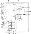
- the AD converter 10 of this embodiment is mounted on an IC (that is, integrated circuit) chip 20 as shown in FIG. 1, and external voltages of analog signals input from external input units 31 and 32 are
- the digital signal is configured to be AD converted.
- the first detection voltage V1 as an external voltage is input to the IC chip 20 from the first input portion 31, and the external voltage is output from the second input portion 32.
- the second detection voltage V2 is input will be described.
- detection voltages as external voltages may be input to the IC chip 20 from a plurality of input units.
- the AD converter 10 includes a multiplexer (ie, MPX) 11, a sample and hold (hereinafter simply referred to as S / H) circuit 12, a conversion unit 13, a reference voltage input unit 14, and a control unit 15. There is.
- MPX multiplexer
- S / H sample and hold
- the multiplexer 11 is connected to the first input portion 31 via the first signal line 41 and connected to the second input portion 32 via the second signal line 42.
- the first signal line 41 is a signal line 41 a such as a wire disposed between the connection terminal 21 of the IC chip 20 and the terminal of the first input unit 31, the connection terminal 21 and the inside of the IC chip 20.
- a signal line 41b such as a wiring pattern formed on the substrate.
- the second signal line 42 is formed in the signal line 42 a such as a wire disposed between the connection terminal 21 of the IC chip 20 and the terminal of the second input section 32, the connection terminal 21 and the IC chip 20.
- the signal line 42b such as the wiring pattern.
- the multiplexer 11 corresponds to a switching unit.
- the multiplexer 11 selects one input signal from the plurality of input signals input based on the control signal from the control unit 15 and outputs the selected input signal to the S / H circuit 12.
- the multiplexer 11 receives, as an input signal, the first detection voltage V1 from the first input unit 31 and the second detection voltage V2 from the second input unit 32. Further, although specifically described later, the multiplexer 11 receives the first reference voltage Vref1 from the reference voltage input unit 14 as the input signal and the second reference voltage Vref2.
- the first input unit 31 and the second input unit 32 are composed of various sensors such as a pressure sensor, a temperature sensor, an acceleration sensor, an angular velocity sensor, etc.
- a ground circuit connected to the In the present embodiment the ground circuit is configured to have a capacitor or the like disposed between the ground and the output terminal of each of the input units 31 and 32, and also functions as a filter circuit for reducing noise.
- a general filter circuit is used as the ground circuit.
- the S / H circuit 12 has a switch 12a connected between the multiplexer 11 and the conversion unit 13, and a capacitor 12b connected between the connection point between the switch 12a and the conversion unit 13 and the ground. doing.
- the switch 12 a When the switch 12 a is turned on, the S / H circuit 12 is connected to the multiplexer 11, and the capacitor 12 b is in a charge state based on the voltage input from the multiplexer 11. That is, the S / H circuit 12 holds the voltage input from the multiplexer 11 when the switch 12 a is turned on.
- the conversion unit 13 is configured to have a comparator or the like, and quantizes a voltage between the conversion reference voltage (for example, 5 V) applied from the reference power supply 13 a and the ground voltage (that is, a predetermined voltage) That is, it is configured to be able to be digitized. Then, the conversion unit 13 converts the voltage held by the S / H circuit 12 into a digital signal based on the control signal from the control unit 15, and outputs the digital signal to the control unit 15.
- the conversion reference voltage for example, 5 V
- the ground voltage that is, a predetermined voltage
- the reference voltage input unit 14 is configured to have a power supply 14 a, a resistor 14 b, and the like, and is connected to the multiplexer 11 via signal lines 51 and 52 such as wiring patterns and inputs a plurality of reference voltages to the multiplexer 11 .
- the reference voltage input unit 14 inputs the first reference voltage Vref1 to the multiplexer 11 through the signal line 51, and inputs the second reference voltage Vref2 through the signal line 52.
- the first reference voltage Vref1 is a value corresponding to the voltage of the power supply 14a
- the second reference voltage Vref2 is a ground voltage (that is, 0 V).
- the control unit 15 is a control circuit which includes, for example, a microcomputer, a storage unit such as a memory, and peripheral circuits thereof, and executes predetermined processing according to a program stored in the storage unit or the like.
- the control unit 15 is connected to the multiplexer 11, the S / H circuit 12, the conversion unit 13, an external circuit, and the like.
- the control unit 15 determines and changes the input signal selected by the multiplexer 11 by inputting a control signal to the multiplexer 11. Further, the control unit 15 switches the on state and the off state of the switch 12 a by inputting a control signal to the S / H circuit 12. Furthermore, the control unit 15 inputs a control signal to the conversion unit 13 to cause the conversion unit 13 to perform AD conversion and input the converted digital signal to the control unit 15. Then, when the digital signal is input from the conversion unit 13, the control unit 15 performs predetermined processing while storing the digital signal in the storage unit as needed. In the present embodiment, as one of the predetermined processes, the control unit 15 determines whether or not a break occurs in the first and second signal lines 41 and 42 between the multiplexer 11 and each of the input units 31 and 32. Execute the disconnection judgment of.
- the control unit 15 when the disconnection determination is performed, the control unit 15 does not allow the multiplexer 11 to select the detection voltage input through the signal line determined in the disconnection determination.
- a reference voltage different in value from the detection voltage is selected.
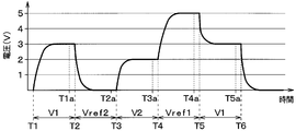
- the normal range of the first detection voltage V1 is 0 to 3 V
- the normal range of the second detection voltage V2 is 2 to 5 V
- the first reference voltage Vref1 is 5 V.
- the voltage Vref2 is set to 0V. Therefore, when the control unit 15 performs the disconnection determination of the first signal line 41, the first reference voltage Vref1 is selected before the multiplexer 11 selects the first detection voltage V1.
- the control unit 15 executes the disconnection determination of the second signal line 42, the second reference voltage Vref2 is selected before the multiplexer 11 selects the second detection voltage V2. Let's do it. Then, the control unit 15 determines whether or not the first signal line 41 is disconnected based on the digital signal corresponding to the first detection voltage V1 and the digital signal corresponding to the first reference voltage Vref1 (see FIG. Hereinafter, the first disconnection judgment is simply performed. In addition, the control unit 15 determines whether or not the second signal line 42 is disconnected based on the digital signal corresponding to the second detection voltage V2 and the digital signal corresponding to the second reference voltage Vref2 Hereinafter, the second disconnection judgment is simply performed.
- the normal range of the first detection voltage V1 is a possible range of the first detection voltage V1 and corresponds to a first predetermined range.
- the normal range of the second detection voltage V2 is a possible range of the second detection voltage V2, and corresponds to a second predetermined range.
- the normal range of the first detection voltage V1 is 0 to 3 V
- the normal range of the second detection voltage V2 is 2 to 5 V
- the first reference voltage Vref1 is 5 V
- the second reference voltage Vref2 is 0 V.
- the first detection voltage V1 when the first detection voltage V1 is selected by the multiplexer 11 is 3 V
- the second detection voltage V2 when the second detection voltage V2 is selected is An example of 2V will be described.
- 2A to 2C show the voltages selected by the multiplexer 11 during each time point. Then, for example, the following processing may be performed continuously and always, may be performed only when the IC chip 20 is activated, or may be performed every predetermined period. It is also good.
- the control unit 15 causes the multiplexer 11 to select the first detection voltage V1 at time T1, and turns on the switch 12a. Thereby, the charge based on the first detection voltage V1 is accumulated in the capacitor 12b, and the capacitor 12b becomes a voltage corresponding to the first detection voltage V1. Then, the control unit 15 turns off the switch 12a at time T1a, causes the conversion unit 13 to generate a digital signal based on the voltage of the capacitor 12b, and inputs the digital signal. Thereafter, predetermined processing using the digital signal is performed.
- the control unit 15 causes the multiplexer 11 to select the second reference voltage Vref2, and turns on the switch 12a.
- the first detection voltage V1 selected at time T1 is 3V
- the second reference voltage Vref2 is 0V.
- the accumulated charge is released from the ground of the reference voltage input unit 14, and the capacitor 12b becomes a voltage corresponding to the second reference voltage Vref2.
- the control unit 15 turns off the switch 12a, causes the conversion unit 13 to generate a digital signal based on the voltage of the capacitor 12b, and causes the digital signal to be input. Thereafter, predetermined processing using the digital signal is performed.
- the control unit 15 causes the multiplexer 11 to select the second detection voltage V2 and turns on the switch 12a. Thereby, the electric charge based on the 2nd detection voltage V2 is accumulate
- the capacitor 12b has a voltage corresponding to the second detection voltage V2.
- the voltage of the capacitor 12b does not change. . That is, the digital signal generated at time point T2a and the digital signal generated at time point T3a become the same signal. Therefore, when the digital signal generated at the time point T2a and the digital signal generated at the time point T3a are the same signal, the control unit 15 determines that the second signal line 42 is disconnected. And outputs a control signal to notify an external circuit or the like of the occurrence of disconnection.
- the normal range of the second detection voltage V2 is 2 to 5 V
- the second reference voltage Vref2 is 0 V. Therefore, when no disconnection occurs in the second signal line 42, a digital signal having a value different from the digital signal is generated before the digital signal corresponding to the second detection voltage V2 is generated. . Therefore, the control unit 15 can easily execute the second disconnection determination by determining whether or not the digital signal generated at the time point T2a matches the digital signal generated at the time point T3a. Further, in the present embodiment, the second disconnection determination is performed by determining whether the digital signals coincide with each other. However, the determination is performed based on the second reference held by the capacitor 12 b of the S / H circuit 12. It can be said that the determination is based on the change in voltage between the voltage Vref2 and the second detection voltage V2.
- the same signal in the present specification means that they are substantially the same signal including the influence of a conversion error, a leak current, and the like.
- the coincidence of two digital signals in the present specification means that they substantially coincide including the effects of conversion error, leakage current, and the like. That is, when comparing the two digital signals, the control unit 15 adds the two digital signals when the change between the two digital signals is within a predetermined range, in addition to the case where the two digital signals completely match. It is determined that the two match. Then, when executing the disconnection determination, the control unit 15 determines that the disconnection occurs when the difference between the two digital signals is within the predetermined range.
- the second disconnection determination performed by the control unit 15 is performed when the voltage change between the second reference voltage Vref2 and the second detection voltage V2 held by the capacitor 12b of the S / H circuit 12 is within a predetermined range. It can be said that it is determined that the second signal line 42 is broken.
- the control unit 15 causes the multiplexer 11 to select the first reference voltage Vref1 and turns on the switch 12a at time T4.
- the second detection voltage V2 selected at time T3 is 2V
- the first reference voltage Vref1 is 5V. Therefore, the charge based on the voltage of the first reference voltage Vref1 is accumulated in the capacitor 12b, and the capacitor 12b has a voltage corresponding to the first reference voltage Vref1.
- the control unit 15 turns off the switch 12a at time point T4a, causes the conversion unit 13 to generate a digital signal based on the voltage of the capacitor 12b, and inputs the digital signal. Thereafter, predetermined processing using the digital signal is performed.
- the control unit 15 causes the multiplexer 11 to select the first detection voltage V1 and turns on the switch 12a.
- the first detection voltage V1 selected at time T5 is 3V
- the first reference voltage Vref1 is 5V. Therefore, in the capacitor 12b, a part of the accumulated charge is released from the ground in the ground circuit in the first input unit 31, and becomes a voltage corresponding to the first detection voltage V1.
- the control unit 15 turns off the switch 12a at time T5a, causes the conversion unit 13 to generate a digital signal based on the voltage of the capacitor 12b, and inputs the digital signal. Thereafter, predetermined processing using the digital signal is performed. Specifically, at this time, the control unit 15 executes the first disconnection determination as one of the predetermined processes.
- the capacitor 12b has a voltage corresponding to the first detection voltage V1.
- the voltage of the capacitor 12b does not change even if the multiplexer 11 selects the first detection voltage V1 as shown in FIG. 2C. . That is, the digital signal generated at time point T4a and the digital signal generated at time point T5a become the same signal. Therefore, when the digital signal generated at the time point T4a and the digital signal generated at the time point T5a are the same signal, the control unit 15 determines that the first signal line 41 is broken. And outputs a control signal to notify an external circuit or the like of the occurrence of an abnormality.
- FIG. 2C shows the voltage of the capacitor 12b when a break occurs in the first signal line 41 between time point T2 and time point T5.
- the normal range of the first detection voltage V1 is 0 to 3 V, and the first reference voltage Vref1 is 5 V. Therefore, when no disconnection occurs in the first signal line 41, a digital signal having a value different from that of the digital signal is generated before the digital signal corresponding to the first detection voltage V1 is generated. . Therefore, the control unit 15 can easily execute the first disconnection determination by determining whether or not the digital signal generated at the time point T4a matches the digital signal generated at the time point T5a. Further, in the present embodiment, the first disconnection determination is performed by determining whether or not the digital signals coincide with each other. However, the determination is made based on the first reference held by the capacitor 12b of the S / H circuit 12.
- the determination is based on the presence or absence of a change in voltage between the voltage Vref1 and the first detection voltage V1. Then, the control unit 15 executes the first disconnection determination as described above. Therefore, the first disconnection determination is performed when the voltage change between the first reference voltage Vref1 and the first detection voltage V1 held by the capacitor 12b of the S / H circuit 12 is within the predetermined range. It can be said that it is determined that a break has occurred in the
- control unit 15 After that, the control unit 15 performs the same processing as that after time T2 after time T6.
- the multiplexer 11 before causing the multiplexer 11 to select the detection voltage input through the signal line determined by the disconnection determination, the multiplexer 11 selects the reference voltage having a value different from the detection voltage. ing. And disconnection determination is performed based on the presence or absence of the change of the voltage hold
- the first reference voltage Vref1 has a value different from the normal range of the first detection voltage V1
- the second reference voltage Vref2 has a value different from the normal range of the second detection voltage V2. It is like that.
- the control unit 15 causes the multiplexer 11 to select the first reference voltage Vref1 before the first detection voltage V1. For this reason, the control unit 15 easily performs the first disconnection determination by determining whether the digital signal corresponding to the first detection voltage V1 matches the digital signal corresponding to the first reference voltage Vref1. be able to.
- 0 V can be included as a normal range of the first detection voltage V1, and the application range can be expanded.
- the control unit 15 when the second disconnection determination is performed, the control unit 15 causes the multiplexer 11 to select the second reference voltage Vref2 before the second detection voltage V2. Therefore, the control unit 15 can easily perform the second disconnection determination by determining whether the digital signal corresponding to the second detection voltage V2 matches the digital signal corresponding to the second reference voltage Vref2. Can. By performing the second disconnection determination in this manner, 5 V can be included as a normal range of the second detection voltage V2 in addition to the above range.
- the present embodiment is also applicable to the case where three or more detection voltages are input to the AD converter 10.
- the reference voltages may be appropriately added and adjusted in accordance with the normal range of each detection voltage.
- the control unit 15 causes the multiplexer 11 to select a reference voltage having a value different from the normal range of the detection voltage before each detection voltage, and compares the digital signal of the detection voltage with the digital signal of the reference voltage. Therefore, the disconnection determination may be performed.
- the present embodiment is the one in which the configuration of the AD conversion device 10 is modified from the first embodiment, and the other parts are the same as the first embodiment, and thus the description thereof is omitted here.
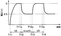
- the multiplexer 11 is connected to the third input unit 33 via the third signal line 43 together with the first input unit 31 and the second input unit 32.
- the third signal line 43 has the same configuration as the first and second signal lines 41 and 42. That is, the third signal line 43 is formed in the signal line 43 a such as a wire disposed between the connection terminal 21 of the IC chip 20 and the terminal of the third input unit 33, the connection terminal 21 and the IC chip 20. And a signal line 43b such as a wiring pattern.
- the multiplexer 11 receives the third detection voltage V3 from the third input unit 33 together with the first detection voltage V1 and the second detection voltage V2.
- the normal value of the third detection voltage V3 is 0V or 5V. That is, the normal value of the third detection voltage V3 is made equal to the first reference voltage Vref1 or the second reference voltage Vref2.
- the third detection voltage V3 corresponds to a third external voltage
- 5 V corresponds to a first voltage
- 0 V corresponds to a second voltage.
- the reference voltage input unit 14 is configured to input the third reference voltage Vref3 through the signal line 53 to the multiplexer 11 in addition to the first reference voltage Vref1 and the second reference voltage Vref2.
- the third reference voltage Vref3 is a voltage obtained by dividing the voltage of the power supply 14a, and is about 2.5V. That is, the third reference voltage Vref3 is a value between possible values of the third detection voltage V3.
- the control unit 15 has the same configuration as that of the first embodiment, but in the present embodiment, a disconnection occurs in the third signal line 43 between the third input unit 33 and the multiplexer 11.
- a third disconnection determination (hereinafter also referred to simply as a third disconnection determination) as to whether or not there is present is performed.
- FIGS. 4A and 4B showing the voltage of the capacitor 12b.
- the operation of the control unit 15 with respect to the first detection voltage V1, the second detection voltage V2, the first reference voltage Vref1, and the second reference voltage Vref2 is the same as that of the first embodiment, and hence the third detection voltage is described below. Only the relationship between V3 and the third reference voltage Vref3 will be described. In the following, an example in which the third detection voltage V3 is 5 V when the third detection voltage V3 is selected by the multiplexer 11 will be described. 4A and 4B show the voltage selected by the multiplexer 11 during each time point.
- the control unit 15 causes the multiplexer 11 to select the third detection voltage V3 and turns on the switch 12a. Thereby, the charge based on the third detection voltage V3 is accumulated in the capacitor 12b, and the capacitor 12b becomes a voltage corresponding to the third detection voltage V3. Then, at time T11a, the control unit 15 turns off the switch 12a, causes the conversion unit 13 to generate a digital signal based on the voltage of the capacitor 12b, and causes the digital signal to be input. Thereafter, predetermined processing using the digital signal is performed.
- the control unit 15 causes the multiplexer 11 to select the third reference voltage Vref3 and turns on the switch 12a.
- the capacitor 12b discharges the accumulated charge from the ground of the reference voltage input unit 14
- the third reference voltage Vref3 is obtained.
- the control unit 15 turns off the switch 12a, causes the conversion unit 13 to generate a digital signal based on the voltage of the capacitor 12b, and causes the digital signal to be input. Thereafter, predetermined processing using the digital signal is performed.
- the control unit 15 causes the multiplexer 11 to select the third detection voltage V3 and turns on the switch 12a.
- the third detection voltage V3 selected at time T13 is 5V
- the third reference voltage Vref3 is 2.5V. Therefore, when no disconnection occurs in the third signal line 43, charges corresponding to the third detection voltage V3 are accumulated in the capacitor 12b, and the capacitor 12b becomes a voltage corresponding to the third detection voltage V3.
- the control unit 15 turns off the switch 12a at time T13a, causes the conversion unit 13 to generate a digital signal based on the voltage of the capacitor 12b, and inputs the digital signal. Thereafter, predetermined processing using the digital signal is performed. Specifically, at this point, the control unit 15 executes the third disconnection determination as one of the predetermined processes.
- the capacitor 12b has a voltage corresponding to the third detection voltage V3.
- the voltage of the capacitor 12b does not change. . That is, the digital signal generated at time T12a and the digital signal generated at time T13a become the same signal. Therefore, when the digital signal generated at time T12a and the digital signal generated at time T13a are the same signal, the control unit 15 determines that the third signal line 43 is broken. And outputs a control signal to notify an external circuit or the like of the occurrence of an abnormality.
- FIG. 4B shows the voltage of the capacitor 12b when a break occurs in the third signal line 43 between time point T12 and time point T13.
- the normal value of the third detection voltage V3 is 0V or 5V
- the third reference voltage Vref3 is 2.5V. Therefore, when no disconnection occurs in the third signal line 43, a digital signal having a value different from that of the digital signal is generated before the digital signal corresponding to the third detection voltage V3 is generated. . Therefore, the control unit 15 can easily execute the third disconnection determination by determining whether the digital signal generated at the time T12a and the digital signal generated at the time T13a coincide with each other. Further, in the present embodiment, the third disconnection determination is performed by determining whether or not the digital signals coincide with each other. However, the determination is performed based on the third criterion held by the capacitor 12b of the S / H circuit 12.
- the determination is based on the presence or absence of a change in voltage between the voltage Vref3 and the third detection voltage V3.
- the control part 15 is performing 3rd disconnection determination as mentioned above. Therefore, the third disconnection determination is performed when the voltage change between the third reference voltage Vref3 and the third detection voltage V3 held by the capacitor 12b of the S / H circuit 12 is within the predetermined range. It can be said that it is determined that a break has occurred in the
- control unit 15 performs the same processing as that after time T12 after time T14.
- the third detection voltage V3 to be selected is 5 V
- the same applies to the case in which the third detection voltage to be selected is 0 V.
- the third detection voltage V3 which is one of two voltages is input through the third signal line 43, and the third reference voltage Vref3 is the third 3 is different from the detection voltage V3. Then, when the third disconnection determination is performed, the control unit 15 causes the multiplexer 11 to select the third reference voltage Vref3 before the third detection voltage V3. Therefore, the control unit 15 easily performs the third disconnection determination by determining whether or not the digital signal corresponding to the third detection voltage V3 matches the digital signal corresponding to the third reference voltage Vref3. be able to.
- disconnection determination of the third signal line 43 to which the third detection voltage V3 which is one of the two voltages is input can also be executed, and the applicable range of the detection voltage can be expanded. .
- the third reference voltage Vref3 has a value different from that of the third detection voltage V3 and is a value between the first reference voltage Vref1 and the second reference voltage Vref2. Therefore, the resistor 14b may be appropriately added to the reference voltage input unit 14 that generates the first reference voltage Vref1 and the second reference voltage Vref2, and the circuit can be prevented from being complicated.
- an abnormality determination as to whether or not an abnormality has occurred in the reference voltage input unit 14 can also be performed with respect to the first embodiment, and the other respects are the same as in the first embodiment. The description is omitted here because it is present.
- the AD converter 10 of this embodiment has the same configuration as that of the first embodiment.
- the control unit 15 of the present embodiment performs abnormality determination including whether or not an abnormality has occurred in the reference voltage input unit 14.
- the abnormality in the reference voltage input unit 14 here is a break in the signal lines 51 and 52 connecting the reference voltage input unit 14 and the multiplexer 11.
- the case is included. That is, the occurrence of abnormality in the reference voltage input unit 14 here means that a failure has occurred in the reference voltage input unit 14 and that a break has occurred in the signal lines 51 and 52. It means that at least one of them is occurring.
- the occurrence of at least one of the failure in the reference voltage input unit 14 and the disconnection of the signal line 51 is also referred to as a first abnormality, and it is determined whether the first abnormality has occurred or not. 1 It is also called an abnormality judgment.
- the occurrence of at least one of a failure in the reference voltage input unit 14 and a break in the signal line 52 is also referred to as a second abnormality, and it is determined whether a second abnormality has occurred or not. It is also called an abnormality judgment.
- the normal range of the first detection voltage V1 is 0 to 3 V
- the normal range of the second detection voltage V2 is 2 to 5 V
- the first reference voltage Vref1 is 5 V.
- the second reference voltage Vref2 will be described as being 0V.
- the first detection voltage V1 when the first detection voltage V1 is selected by the multiplexer 11 is 3V
- the second detection voltage V2 when the second detection voltage V2 is selected is 2V.
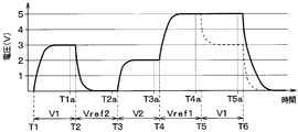
- 5A to 5C show voltages selected by the multiplexer 11 during each time point.
- control unit 15 performs the same process as at time T1, and at time T21a, performs the same process as time T1a.
- the control unit 15 causes the multiplexer 11 to select the first reference voltage Vref1, and turns on the switch 12a.
- the first detection voltage V1 selected at time T21 is 3V
- the first reference voltage Vref1 is 5V. Therefore, the charge based on the voltage of the first reference voltage Vref1 is accumulated in the capacitor 12b, and the capacitor 12b has a voltage corresponding to the first reference voltage Vref1.
- the control unit 15 turns off the switch 12a, causes the conversion unit 13 to generate a digital signal based on the charge accumulated in the capacitor, and causes the digital signal to be input. Thereafter, predetermined processing using the digital signal is performed.
- the control unit 15 causes the multiplexer 11 to select the second reference voltage Vref2, and turns on the switch 12a.
- the first reference voltage Vref1 selected at time T22 is 5V
- the second reference voltage Vref2 is 0V.
- the control unit 15 turns off the switch 12a at time T23a, causes the conversion unit 13 to generate a digital signal based on the voltage of the capacitor 12b, and inputs the digital signal.
- predetermined processing using the digital signal is performed. Specifically, at this time, the control unit 15 executes the second abnormality determination as one of the predetermined processes.
- the capacitor 12b has a voltage corresponding to the second reference voltage Vref2.
- the voltage of the capacitor 12b does not change. That is, the digital signal generated at time T22a and the digital signal generated at time T23a become the same signal. Therefore, when the digital signal generated at time T22a and the digital signal generated at time T23a are the same signal, the control unit 15 determines that the second abnormality has occurred, and the external circuit or the like Outputs a control signal to notify that the second abnormality has occurred.
- the normal range of the first detection voltage V1 is 0 to 3 V
- the second reference voltage Vref2 is 0 V. Therefore, immediately after the first detection voltage V1, the second reference voltage Vref2 is converted into a digital signal, and the digital signal corresponding to the first detection voltage V1 is compared with the digital signal corresponding to the second reference voltage Vref2. If so, the second abnormality determination may not be possible. That is, when 0 V is input as the first detection voltage V1, the first detection voltage V1 and the second reference voltage Vref2 become the same, and it can not be determined whether the second abnormality occurs. Therefore, in the present embodiment, the first reference voltage Vref1 is converted to a digital signal before the second reference voltage Vref2.
- the control unit 15 can easily execute the second abnormality determination by determining whether the digital signal generated at the time point T22a and the digital signal generated at the time point T23a coincide with each other. Further, in the present embodiment, the second abnormality determination is performed by determining whether the digital signals coincide with each other, but the determination is made based on the first reference held by the capacitor 12 b of the S / H circuit 12. It can be said that this determination is based on the presence or absence of a change in voltage between the voltage Vref1 and the second reference voltage Vref2. And the control part 15 is performing 2nd abnormality determination as mentioned above.
- the second abnormality occurs when the voltage change between the first reference voltage Vref1 and the second reference voltage Vref2 held by the capacitor 12b of the S / H circuit 12 is within a predetermined range. It can be said that it is determined that the
- control unit 15 performs processing similar to that at time T3 at time T24, and performs processing similar to that at time T3a at time T24a.
- the control unit 15 causes the multiplexer 11 to select the second reference voltage Vref2, and turns on the switch 12a.
- the second detection voltage V2 selected at time T24 is 2V
- the second reference voltage Vref2 is 0V.
- the control unit 15 turns off the switch 12a at time T25a, causes the conversion unit 13 to generate a digital signal based on the voltage of the capacitor 12b, and inputs the digital signal. Thereafter, predetermined processing using the digital signal is performed.
- the control unit 15 causes the multiplexer 11 to select the first reference voltage Vref1, and turns on the switch 12a. Thereby, the charge based on the first reference voltage Vref1 is accumulated in the capacitor 12b, and the capacitor 12b becomes a voltage corresponding to the first reference voltage Vref1. Then, the control unit 15 turns off the switch 12a at time T26a, causes the conversion unit 13 to generate a digital signal based on the voltage of the capacitor 12b, and inputs the digital signal. Thereafter, predetermined processing using the digital signal is performed. Specifically, at this time, the control unit 15 executes the first abnormality determination as one of the predetermined processes.
- the capacitor 12b has a voltage corresponding to the first reference voltage Vref1.
- the voltage of the capacitor 12b does not change. That is, the digital signal generated at time T25a and the digital signal generated at time T26a become the same signal. Therefore, when the digital signal generated at time T25a and the digital signal generated at time T26a are the same signal, the control unit 15 determines that the first abnormality has occurred, and the external circuit or the like Output a control signal to notify the error occurrence.
- FIG. 5C shows the voltage of the capacitor 12b when the first abnormality occurs between time point T23 and time point T26.
- the normal range of the second detection voltage V2 is 2 to 5 V
- the first reference voltage Vref1 is 5 V. Therefore, immediately after the second detection voltage V2, the first reference voltage Vref1 is converted to a digital signal, and the digital signal corresponding to the second detection voltage V2 is compared with the digital signal corresponding to the first reference voltage Vref1. If this is the case, the first abnormality determination may not be possible. That is, when 5 V is input as the second detection voltage V2, the second detection voltage V2 and the first reference voltage Vref1 become the same, and it can not be determined whether or not the first abnormality occurs.
- the second reference voltage Vref2 is converted to a digital signal before the first reference voltage Vref1. Then, when the first abnormality does not occur, a digital signal different from the digital signal is generated before the first reference voltage Vref1 is converted into the digital signal.
- the control unit 15 can easily execute the first abnormality determination by determining whether the digital signal generated at the time point T25a matches the digital signal generated at the time point T26a. Further, in the present embodiment, the first disconnection determination is performed by determining whether or not the digital signals coincide with each other. However, the determination is performed based on the second reference held by the capacitor 12b of the S / H circuit 12.
- the determination is based on the presence or absence of a change in voltage between the voltage Vref2 and the first reference voltage Vref1. Then, the control unit 15 executes the first abnormality determination as described above. Therefore, in the first abnormality determination, the first abnormality occurs when the voltage change between the second reference voltage Vref2 and the first reference voltage Vref1 held by the capacitor 12b of the S / H circuit 12 is within a predetermined range. It can be said that it is determined that the
- control unit 15 performs processing similar to that at time T5 at time T27, and performs processing similar to that at time T5a at time T27a. Thereafter, the control unit 15 performs the same processing as that after time T22 after time T28.
- the abnormality of the AD converter 10 can be determined with higher accuracy.
- the multiplexer 11 selects the second reference voltage Vref2 before the first reference voltage Vref1. Further, when the second abnormality determination is performed, the control unit 15 causes the multiplexer 11 to select the first reference voltage Vref1 before the second reference voltage Vref2. Therefore, the control unit 15 can easily determine the first abnormality and the second abnormality by determining whether the digital signal corresponding to the first reference voltage Vref1 matches the digital signal corresponding to the second reference voltage Vref2. Abnormality determination can be performed.
- control unit 15 changes the order of the voltages selected by the multiplexer 11 to perform the first abnormality determination and the second abnormality determination. That is, in the present embodiment, it is not necessary to add a new circuit to perform the first abnormality determination and the second abnormality determination. Therefore, in the present embodiment, the first abnormality determination and the second abnormality determination can be executed while suppressing an increase in circuit scale.
- This embodiment changes the normal range of the first detection voltage V1 and the second detection voltage V2 with respect to the first embodiment, and further performs the first abnormality determination and the second abnormality determination as in the third embodiment. It is intended to The other aspects are the same as in the first embodiment, and thus the description thereof is omitted here.
- the AD converter 10 of this embodiment has the same configuration as that of the first embodiment.
- the normal range of the first detection voltage V1 is 1 to 3 V
- the normal range of the second detection voltage V2 is 2 to 4 V. That is, the first reference voltage Vref1 and the second reference voltage Vref2 have different values from the first detection voltage V1 and the second detection voltage V2, respectively.
- the normal range of the first detection voltage V1 is 1 to 3 V
- the normal range of the second detection voltage V2 is 2 to 4 V
- the first reference voltage Vref1 is 5 V
- the second reference voltage Vref2 is 0V.
- the first detection voltage V1 when the first detection voltage V1 is selected by the multiplexer 11 is 3 V
- the second detection voltage V2 when the second detection voltage V2 is selected is An example of 2V will be described.
- 6A and 6B show the voltages selected by the multiplexer 11 during each time point.
- control unit 15 of the present embodiment is basically the same as that described in the first embodiment. Then, at time T2a, the control unit 15 executes the second abnormality determination as one of the predetermined processes.
- the capacitor 12b changes from time T2 to a voltage according to the second reference voltage Vref2.
- the second reference voltage Vref2 is selected by the multiplexer 11
- the voltage of the capacitor 12b does not change. That is, the digital signal generated at time point T1a and the digital signal generated at time point T2a become the same signal. Therefore, when the digital signal generated at the time point T1a and the digital signal generated at the time point T2a are the same signal, the control unit 15 determines that the second abnormality has occurred, and the external circuit etc. Output a control signal to notify the error occurrence.
- the normal range of the first detection voltage V1 is 1 to 3 V
- the second reference voltage Vref2 is 0 V. Therefore, when the second abnormality does not occur, the digital signal having a value different from the digital signal is generated before the digital signal corresponding to the second reference voltage Vref2 is generated. Therefore, the control unit 15 can easily execute the second abnormality determination by determining whether or not the digital signal generated at the time point T1a matches the digital signal generated at the time point T2a. And the control part 15 is performing 2nd abnormality determination as mentioned above.
- the second abnormality occurs when the voltage change between the first detection voltage V1 and the second reference voltage Vref2 held by the capacitor 12b of the S / H circuit 12 is within a predetermined range. It can be said that it is determined that the
- control unit 15 executes the first abnormality determination as one of the predetermined processes.
- control unit 15 determines that the first abnormality has occurred, and the external circuit or the like Output a control signal to notify the error occurrence.
- the normal range of the second detection voltage V2 is 2 to 4 V
- the first reference voltage Vref1 is 5 V. Therefore, when the first abnormality does not occur, a digital signal having a value different from that of the digital signal is generated before the digital signal corresponding to the first reference voltage Vref1 is generated. Therefore, the control unit 15 can easily execute the first abnormality determination by determining whether the digital signal generated at the time point T3a matches the digital signal generated at the time point T4a. Then, the control unit 15 executes the first abnormality determination as described above.
- the first abnormality occurs when the voltage change between the second detection voltage V2 held by the capacitor 12b of the S / H circuit 12 and the first reference voltage Vref1 is within a predetermined range. It can be said that it is determined that the
- the first reference voltage Vref1 and the second reference voltage Vref2 have different values from the first detection voltage V1 and the second detection voltage V2. Therefore, even if the second detection voltage V2 is selected by the multiplexer 11 before the first reference voltage Vref1, the digital signal according to the first reference voltage Vref1 and the digital signal according to the second detection voltage V2 Are different values. That is, the second detection voltage V2 used in the second disconnection determination can be used as it is. Similarly, even if the first detection voltage V1 is selected by the multiplexer 11 before the second reference voltage Vref2, a digital signal corresponding to the second reference voltage Vref2 and a digital signal corresponding to the first detection voltage V1 are used. Are different values. That is, the first detection voltage V1 used in the first disconnection determination can be used as it is.
- the second reference voltage Vref2 does not have to be selected by the multiplexer 11 to perform the first abnormality determination, and the first abnormality determination is performed.
- the reference voltage Vref1 does not have to be selected by the multiplexer 11. Therefore, according to the present embodiment, it is possible to shorten the total period required to perform all the determinations of the first disconnection determination, the second disconnection determination, the first abnormality determination, and the second abnormality determination.
- the first reference voltage Vref1 and the second reference voltage Vref2 have different values from the first detection voltage V1 and the second detection voltage V2. Therefore, even if the first reference voltage Vref1 is converted before the second detection voltage V2, the second detection voltage V2 and the first reference voltage Vref1 have different values. Therefore, the first reference voltage Vref1 may be converted before the second detection voltage V2. Similarly, the second reference voltage Vref2 may be converted before the first detection voltage V1.
- the multiplexer 11, the S / H circuit 12, the conversion unit 13, the reference voltage input unit 14, and the control unit 15 may not be mounted on the common IC chip 20.
- the reference voltage input unit 14 may not be mounted on the IC chip 20 but may be mounted on another chip. .
- the reference voltage input unit 14 may not be mounted on the IC chip 20.
- control unit 15 is not mounted on the IC chip 20, and a vehicle ECU (ie, An Engine Control Unit) may perform the function of the control unit 15 of each of the above embodiments.
- a vehicle ECU ie, An Engine Control Unit
- a plurality of control units 15 may be provided, and each control unit 15 may perform the above functions.
- a control unit that controls the multiplexer 11, a control unit that controls the S / H circuit 12, and a control unit that controls the conversion unit 13 may be separately provided.
- the conversion reference voltage is input from the reference power supply 13a to the conversion unit 13.
- the conversion unit 13 does not include the reference power supply 13a.
- a reference voltage may be input. According to this, the number of parts can be reduced, and the circuit scale can be further reduced.
- the control unit 15 uses the reference voltage input from the reference voltage input unit 14, and when the conversion unit 13 generates a digital signal according to the reference voltage, based on the digital signal, The abnormality determination of the conversion unit 13 may be performed. That is, the reference voltage input from the reference voltage input unit 14 may be used for another application.
- the reference voltage generation unit that generates the reference voltage for performing the abnormality determination of the conversion unit 13 may have a function as the reference voltage input unit 14 of each of the above embodiments. According to this, it is possible to improve the function while suppressing an increase in the number of parts.
- control unit 15 may directly read the voltage of the capacitor 12b and perform each determination based on the presence or absence of a change in the voltage of the capacitor 12b. Even when the determination is performed in this manner, it is determined that disconnection or abnormality occurs when the change in the voltage of the capacitor 12b is within a predetermined range in consideration of a detection error or the like. Is preferred.
- the resistor 14 b may not be disposed between the power supply 14 a and the multiplexer 11. Similarly, as shown in FIG. 9, the resistor 14 b may not be disposed between the ground of the reference voltage input unit 14 and the multiplexer 11. Although not particularly illustrated, the same applies to the second embodiment.
- the above embodiments may be combined as appropriate.
- the second embodiment may be combined with the third and fourth embodiments, and the third detection voltage V3 may be input from the third input unit 33.
- the storage medium or memory is a non-transitional tangible storage medium.
Landscapes
- Engineering & Computer Science (AREA)
- Theoretical Computer Science (AREA)
- Testing Of Short-Circuits, Discontinuities, Leakage, Or Incorrect Line Connections (AREA)
- Analogue/Digital Conversion (AREA)
Priority Applications (2)
| Application Number | Priority Date | Filing Date | Title |
|---|---|---|---|
| DE112018005329.6T DE112018005329T5 (de) | 2017-09-20 | 2018-09-13 | Analog-digital-wandlungsvorrichtung |
| US16/817,982 US10979061B2 (en) | 2017-09-20 | 2020-03-13 | Analog-digital conversion device |
Applications Claiming Priority (2)
| Application Number | Priority Date | Filing Date | Title |
|---|---|---|---|
| JP2017180510A JP6772993B2 (ja) | 2017-09-20 | 2017-09-20 | アナログ−デジタル変換装置 |
| JP2017-180510 | 2017-09-20 |
Related Child Applications (1)
| Application Number | Title | Priority Date | Filing Date |
|---|---|---|---|
| US16/817,982 Continuation US10979061B2 (en) | 2017-09-20 | 2020-03-13 | Analog-digital conversion device |
Publications (1)
| Publication Number | Publication Date |
|---|---|
| WO2019059104A1 true WO2019059104A1 (ja) | 2019-03-28 |
Family
ID=65809824
Family Applications (1)
| Application Number | Title | Priority Date | Filing Date |
|---|---|---|---|
| PCT/JP2018/034057 Ceased WO2019059104A1 (ja) | 2017-09-20 | 2018-09-13 | アナログ-デジタル変換装置 |
Country Status (4)
| Country | Link |
|---|---|
| US (1) | US10979061B2 (enExample) |
| JP (1) | JP6772993B2 (enExample) |
| DE (1) | DE112018005329T5 (enExample) |
| WO (1) | WO2019059104A1 (enExample) |
Cited By (2)
| Publication number | Priority date | Publication date | Assignee | Title |
|---|---|---|---|---|
| CN110824410A (zh) * | 2019-11-28 | 2020-02-21 | 深圳市锐能微科技有限公司 | 一种参数检测电路及方法 |
| CN110824411A (zh) * | 2019-11-28 | 2020-02-21 | 深圳市锐能微科技有限公司 | 一种参数检测电路及方法 |
Families Citing this family (1)
| Publication number | Priority date | Publication date | Assignee | Title |
|---|---|---|---|---|
| US11837905B2 (en) * | 2021-05-25 | 2023-12-05 | Cyberswitchingpatents, Llc | Battery charger system |
Citations (4)
| Publication number | Priority date | Publication date | Assignee | Title |
|---|---|---|---|---|
| JP2001244813A (ja) * | 2000-02-28 | 2001-09-07 | Hitachi Ltd | 入力回路、断線検出回路及び断線検出方法 |
| JP2005323273A (ja) * | 2004-05-11 | 2005-11-17 | Tokai Rika Co Ltd | A/d変換装置 |
| JP2012245943A (ja) * | 2011-05-31 | 2012-12-13 | Hitachi Automotive Systems Ltd | 制御装置 |
| JP2016025594A (ja) * | 2014-07-23 | 2016-02-08 | リンナイ株式会社 | 制御装置 |
Family Cites Families (13)
| Publication number | Priority date | Publication date | Assignee | Title |
|---|---|---|---|---|
| JPH0856160A (ja) * | 1994-08-10 | 1996-02-27 | Nissin Electric Co Ltd | Adコンバータの異常検出装置 |
| JP3597303B2 (ja) * | 1996-04-23 | 2004-12-08 | 株式会社ルネサステクノロジ | A/dコンバータのテスト方法及びテスト装置 |
| JP2003258639A (ja) * | 2002-02-27 | 2003-09-12 | Nec Microsystems Ltd | アナログ−ディジタル変換器 |
| JP2005026805A (ja) * | 2003-06-30 | 2005-01-27 | Renesas Technology Corp | 半導体集積回路 |
| JP2005167972A (ja) * | 2003-11-12 | 2005-06-23 | Denso Corp | A/d変換処理装置、その使用方法及び電子制御装置 |
| JP3861874B2 (ja) * | 2003-12-16 | 2006-12-27 | 株式会社デンソー | Ad変換器の故障検出装置 |
| JP4375331B2 (ja) * | 2005-12-26 | 2009-12-02 | 株式会社デンソー | ノックセンサ信号処理装置 |
| JP4779793B2 (ja) | 2006-05-01 | 2011-09-28 | 株式会社デンソー | Ad変換装置及び電子制御装置 |
| JP5155012B2 (ja) | 2008-05-23 | 2013-02-27 | ルネサスエレクトロニクス株式会社 | Ad変換器及びデータ処理装置 |
| US8324861B2 (en) * | 2009-03-05 | 2012-12-04 | O2Micro Inc. | Multi-channel converter with self-diagnosis functionality |
| JP2010237079A (ja) * | 2009-03-31 | 2010-10-21 | Renesas Electronics Corp | 断線検出回路及び断線検出方法 |
| JP5866001B2 (ja) * | 2012-04-27 | 2016-02-17 | 日立オートモティブシステムズ株式会社 | 電池監視装置および電池システム監視装置 |
| JP6262788B2 (ja) | 2016-03-28 | 2018-01-17 | 公益財団法人岡山県産業振興財団 | シール構造 |
-
2017
- 2017-09-20 JP JP2017180510A patent/JP6772993B2/ja active Active
-
2018
- 2018-09-13 DE DE112018005329.6T patent/DE112018005329T5/de active Granted
- 2018-09-13 WO PCT/JP2018/034057 patent/WO2019059104A1/ja not_active Ceased
-
2020
- 2020-03-13 US US16/817,982 patent/US10979061B2/en active Active
Patent Citations (4)
| Publication number | Priority date | Publication date | Assignee | Title |
|---|---|---|---|---|
| JP2001244813A (ja) * | 2000-02-28 | 2001-09-07 | Hitachi Ltd | 入力回路、断線検出回路及び断線検出方法 |
| JP2005323273A (ja) * | 2004-05-11 | 2005-11-17 | Tokai Rika Co Ltd | A/d変換装置 |
| JP2012245943A (ja) * | 2011-05-31 | 2012-12-13 | Hitachi Automotive Systems Ltd | 制御装置 |
| JP2016025594A (ja) * | 2014-07-23 | 2016-02-08 | リンナイ株式会社 | 制御装置 |
Cited By (2)
| Publication number | Priority date | Publication date | Assignee | Title |
|---|---|---|---|---|
| CN110824410A (zh) * | 2019-11-28 | 2020-02-21 | 深圳市锐能微科技有限公司 | 一种参数检测电路及方法 |
| CN110824411A (zh) * | 2019-11-28 | 2020-02-21 | 深圳市锐能微科技有限公司 | 一种参数检测电路及方法 |
Also Published As
| Publication number | Publication date |
|---|---|
| US20200220552A1 (en) | 2020-07-09 |
| JP6772993B2 (ja) | 2020-10-21 |
| DE112018005329T5 (de) | 2020-07-02 |
| JP2019057799A (ja) | 2019-04-11 |
| US10979061B2 (en) | 2021-04-13 |
Similar Documents
| Publication | Publication Date | Title |
|---|---|---|
| US20160274610A1 (en) | Electronic control device | |
| JP6291979B2 (ja) | 自己診断機能を有する入力回路 | |
| KR101445424B1 (ko) | 검출 회로 및 센서 장치 | |
| US9083367B2 (en) | Analog-to-digital converter and self-diagnosis method for analog-to-digital converter | |
| WO2019059104A1 (ja) | アナログ-デジタル変換装置 | |
| US9739822B2 (en) | Input circuit | |
| JP6838212B2 (ja) | 電子制御装置 | |
| JP6088642B2 (ja) | 複数のアナログ信号検出チャネルを有するアナログ信号入力回路 | |
| JP2016134010A (ja) | 電源監視回路 | |
| US9356590B1 (en) | Production test trimming acceleration | |
| JP6420960B2 (ja) | 電子制御装置 | |
| JP2017118180A (ja) | A/d変換装置 | |
| JP2012151941A (ja) | 昇圧システム、診断方法、及び診断プログラム | |
| JP2017106811A (ja) | 診断回路、半導体装置、車載用電子制御ユニット及び診断回路による診断方法 | |
| JP2017079427A (ja) | 電子制御装置 | |
| US7477179B2 (en) | Successive approximation A/D converter comparing analog input voltage to reference voltages | |
| JP2017063355A (ja) | 半導体装置 | |
| US11645177B2 (en) | Diagnosis circuit for making a diagnosis of a multiplexer | |
| JP2015033063A (ja) | A/dコンバータのオープン検出装置およびa/dコンバータのオープン検出方法 | |
| JP2000209090A (ja) | A/dコンバ―タ | |
| US20240230730A9 (en) | Device and method for ratiometric measurement of voltages for an analog-digital-converter | |
| JP4797961B2 (ja) | Ad変換回路 | |
| US20150073743A1 (en) | Temperature sensor | |
| JP2018128424A (ja) | 測定装置及び車載充電器 | |
| JP6598928B1 (ja) | 電子制御装置 |
Legal Events
| Date | Code | Title | Description |
|---|---|---|---|
| 121 | Ep: the epo has been informed by wipo that ep was designated in this application |
Ref document number: 18858333 Country of ref document: EP Kind code of ref document: A1 |
|
| 122 | Ep: pct application non-entry in european phase |
Ref document number: 18858333 Country of ref document: EP Kind code of ref document: A1 |