WO2019048967A1 - 半導体装置、記憶装置、及び電子機器 - Google Patents
半導体装置、記憶装置、及び電子機器 Download PDFInfo
- Publication number
- WO2019048967A1 WO2019048967A1 PCT/IB2018/056412 IB2018056412W WO2019048967A1 WO 2019048967 A1 WO2019048967 A1 WO 2019048967A1 IB 2018056412 W IB2018056412 W IB 2018056412W WO 2019048967 A1 WO2019048967 A1 WO 2019048967A1
- Authority
- WO
- WIPO (PCT)
- Prior art keywords
- transistor
- bit line
- circuit
- sense amplifier
- memory cell
- Prior art date
- Legal status (The legal status is an assumption and is not a legal conclusion. Google has not performed a legal analysis and makes no representation as to the accuracy of the status listed.)
- Ceased
Links
Images





Classifications
-
- H—ELECTRICITY
- H10—SEMICONDUCTOR DEVICES; ELECTRIC SOLID-STATE DEVICES NOT OTHERWISE PROVIDED FOR
- H10B—ELECTRONIC MEMORY DEVICES
- H10B41/00—Electrically erasable-and-programmable ROM [EEPROM] devices comprising floating gates
- H10B41/70—Electrically erasable-and-programmable ROM [EEPROM] devices comprising floating gates the floating gate being an electrode shared by two or more components
-
- G—PHYSICS
- G11—INFORMATION STORAGE
- G11C—STATIC STORES
- G11C11/00—Digital stores characterised by the use of particular electric or magnetic storage elements; Storage elements therefor
- G11C11/21—Digital stores characterised by the use of particular electric or magnetic storage elements; Storage elements therefor using electric elements
- G11C11/34—Digital stores characterised by the use of particular electric or magnetic storage elements; Storage elements therefor using electric elements using semiconductor devices
- G11C11/40—Digital stores characterised by the use of particular electric or magnetic storage elements; Storage elements therefor using electric elements using semiconductor devices using transistors
- G11C11/401—Digital stores characterised by the use of particular electric or magnetic storage elements; Storage elements therefor using electric elements using semiconductor devices using transistors forming cells needing refreshing or charge regeneration, i.e. dynamic cells
- G11C11/4063—Auxiliary circuits, e.g. for addressing, decoding, driving, writing, sensing or timing
- G11C11/407—Auxiliary circuits, e.g. for addressing, decoding, driving, writing, sensing or timing for memory cells of the field-effect type
- G11C11/409—Read-write [R-W] circuits
- G11C11/4091—Sense or sense/refresh amplifiers, or associated sense circuitry, e.g. for coupled bit-line precharging, equalising or isolating
-
- G—PHYSICS
- G11—INFORMATION STORAGE
- G11C—STATIC STORES
- G11C11/00—Digital stores characterised by the use of particular electric or magnetic storage elements; Storage elements therefor
- G11C11/21—Digital stores characterised by the use of particular electric or magnetic storage elements; Storage elements therefor using electric elements
- G11C11/34—Digital stores characterised by the use of particular electric or magnetic storage elements; Storage elements therefor using electric elements using semiconductor devices
- G11C11/40—Digital stores characterised by the use of particular electric or magnetic storage elements; Storage elements therefor using electric elements using semiconductor devices using transistors
- G11C11/401—Digital stores characterised by the use of particular electric or magnetic storage elements; Storage elements therefor using electric elements using semiconductor devices using transistors forming cells needing refreshing or charge regeneration, i.e. dynamic cells
- G11C11/403—Digital stores characterised by the use of particular electric or magnetic storage elements; Storage elements therefor using electric elements using semiconductor devices using transistors forming cells needing refreshing or charge regeneration, i.e. dynamic cells with charge regeneration common to a multiplicity of memory cells, i.e. external refresh
- G11C11/404—Digital stores characterised by the use of particular electric or magnetic storage elements; Storage elements therefor using electric elements using semiconductor devices using transistors forming cells needing refreshing or charge regeneration, i.e. dynamic cells with charge regeneration common to a multiplicity of memory cells, i.e. external refresh with one charge-transfer gate, e.g. MOS transistor, per cell
-
- G—PHYSICS
- G11—INFORMATION STORAGE
- G11C—STATIC STORES
- G11C11/00—Digital stores characterised by the use of particular electric or magnetic storage elements; Storage elements therefor
- G11C11/21—Digital stores characterised by the use of particular electric or magnetic storage elements; Storage elements therefor using electric elements
- G11C11/34—Digital stores characterised by the use of particular electric or magnetic storage elements; Storage elements therefor using electric elements using semiconductor devices
- G11C11/40—Digital stores characterised by the use of particular electric or magnetic storage elements; Storage elements therefor using electric elements using semiconductor devices using transistors
- G11C11/401—Digital stores characterised by the use of particular electric or magnetic storage elements; Storage elements therefor using electric elements using semiconductor devices using transistors forming cells needing refreshing or charge regeneration, i.e. dynamic cells
- G11C11/403—Digital stores characterised by the use of particular electric or magnetic storage elements; Storage elements therefor using electric elements using semiconductor devices using transistors forming cells needing refreshing or charge regeneration, i.e. dynamic cells with charge regeneration common to a multiplicity of memory cells, i.e. external refresh
- G11C11/405—Digital stores characterised by the use of particular electric or magnetic storage elements; Storage elements therefor using electric elements using semiconductor devices using transistors forming cells needing refreshing or charge regeneration, i.e. dynamic cells with charge regeneration common to a multiplicity of memory cells, i.e. external refresh with three charge-transfer gates, e.g. MOS transistors, per cell
-
- G—PHYSICS
- G11—INFORMATION STORAGE
- G11C—STATIC STORES
- G11C11/00—Digital stores characterised by the use of particular electric or magnetic storage elements; Storage elements therefor
- G11C11/21—Digital stores characterised by the use of particular electric or magnetic storage elements; Storage elements therefor using electric elements
- G11C11/34—Digital stores characterised by the use of particular electric or magnetic storage elements; Storage elements therefor using electric elements using semiconductor devices
- G11C11/40—Digital stores characterised by the use of particular electric or magnetic storage elements; Storage elements therefor using electric elements using semiconductor devices using transistors
- G11C11/401—Digital stores characterised by the use of particular electric or magnetic storage elements; Storage elements therefor using electric elements using semiconductor devices using transistors forming cells needing refreshing or charge regeneration, i.e. dynamic cells
- G11C11/4063—Auxiliary circuits, e.g. for addressing, decoding, driving, writing, sensing or timing
- G11C11/407—Auxiliary circuits, e.g. for addressing, decoding, driving, writing, sensing or timing for memory cells of the field-effect type
- G11C11/409—Read-write [R-W] circuits
- G11C11/4097—Bit-line organisation, e.g. bit-line layout, folded bit lines
-
- G—PHYSICS
- G11—INFORMATION STORAGE
- G11C—STATIC STORES
- G11C5/00—Details of stores covered by group G11C11/00
- G11C5/02—Disposition of storage elements, e.g. in the form of a matrix array
-
- G—PHYSICS
- G11—INFORMATION STORAGE
- G11C—STATIC STORES
- G11C5/00—Details of stores covered by group G11C11/00
- G11C5/02—Disposition of storage elements, e.g. in the form of a matrix array
- G11C5/025—Geometric lay-out considerations of storage- and peripheral-blocks in a semiconductor storage device
-
- G—PHYSICS
- G11—INFORMATION STORAGE
- G11C—STATIC STORES
- G11C5/00—Details of stores covered by group G11C11/00
- G11C5/06—Arrangements for interconnecting storage elements electrically, e.g. by wiring
- G11C5/063—Voltage and signal distribution in integrated semi-conductor memory access lines, e.g. word-line, bit-line, cross-over resistance, propagation delay
-
- H—ELECTRICITY
- H10—SEMICONDUCTOR DEVICES; ELECTRIC SOLID-STATE DEVICES NOT OTHERWISE PROVIDED FOR
- H10B—ELECTRONIC MEMORY DEVICES
- H10B12/00—Dynamic random access memory [DRAM] devices
- H10B12/30—DRAM devices comprising one-transistor - one-capacitor [1T-1C] memory cells
-
- H—ELECTRICITY
- H10—SEMICONDUCTOR DEVICES; ELECTRIC SOLID-STATE DEVICES NOT OTHERWISE PROVIDED FOR
- H10D—INORGANIC ELECTRIC SEMICONDUCTOR DEVICES
- H10D30/00—Field-effect transistors [FET]
- H10D30/60—Insulated-gate field-effect transistors [IGFET]
- H10D30/67—Thin-film transistors [TFT]
- H10D30/674—Thin-film transistors [TFT] characterised by the active materials
- H10D30/6755—Oxide semiconductors, e.g. zinc oxide, copper aluminium oxide or cadmium stannate
-
- H—ELECTRICITY
- H10—SEMICONDUCTOR DEVICES; ELECTRIC SOLID-STATE DEVICES NOT OTHERWISE PROVIDED FOR
- H10D—INORGANIC ELECTRIC SEMICONDUCTOR DEVICES
- H10D30/00—Field-effect transistors [FET]
- H10D30/60—Insulated-gate field-effect transistors [IGFET]
- H10D30/68—Floating-gate IGFETs
-
- H—ELECTRICITY
- H10—SEMICONDUCTOR DEVICES; ELECTRIC SOLID-STATE DEVICES NOT OTHERWISE PROVIDED FOR
- H10D—INORGANIC ELECTRIC SEMICONDUCTOR DEVICES
- H10D30/00—Field-effect transistors [FET]
- H10D30/60—Insulated-gate field-effect transistors [IGFET]
- H10D30/69—IGFETs having charge trapping gate insulators, e.g. MNOS transistors
-
- H—ELECTRICITY
- H10—SEMICONDUCTOR DEVICES; ELECTRIC SOLID-STATE DEVICES NOT OTHERWISE PROVIDED FOR
- H10B—ELECTRONIC MEMORY DEVICES
- H10B12/00—Dynamic random access memory [DRAM] devices
-
- H—ELECTRICITY
- H10—SEMICONDUCTOR DEVICES; ELECTRIC SOLID-STATE DEVICES NOT OTHERWISE PROVIDED FOR
- H10D—INORGANIC ELECTRIC SEMICONDUCTOR DEVICES
- H10D30/00—Field-effect transistors [FET]
- H10D30/60—Insulated-gate field-effect transistors [IGFET]
- H10D30/67—Thin-film transistors [TFT]
- H10D30/6729—Thin-film transistors [TFT] characterised by the electrodes
- H10D30/673—Thin-film transistors [TFT] characterised by the electrodes characterised by the shapes, relative sizes or dispositions of the gate electrodes
- H10D30/6733—Multi-gate TFTs
- H10D30/6734—Multi-gate TFTs having gate electrodes arranged on both top and bottom sides of the channel, e.g. dual-gate TFTs
-
- H—ELECTRICITY
- H10—SEMICONDUCTOR DEVICES; ELECTRIC SOLID-STATE DEVICES NOT OTHERWISE PROVIDED FOR
- H10D—INORGANIC ELECTRIC SEMICONDUCTOR DEVICES
- H10D30/00—Field-effect transistors [FET]
- H10D30/60—Insulated-gate field-effect transistors [IGFET]
- H10D30/67—Thin-film transistors [TFT]
- H10D30/6757—Thin-film transistors [TFT] characterised by the structure of the channel, e.g. transverse or longitudinal shape or doping profile
-
- H—ELECTRICITY
- H10—SEMICONDUCTOR DEVICES; ELECTRIC SOLID-STATE DEVICES NOT OTHERWISE PROVIDED FOR
- H10D—INORGANIC ELECTRIC SEMICONDUCTOR DEVICES
- H10D86/00—Integrated devices formed in or on insulating or conducting substrates, e.g. formed in silicon-on-insulator [SOI] substrates or on stainless steel or glass substrates
- H10D86/40—Integrated devices formed in or on insulating or conducting substrates, e.g. formed in silicon-on-insulator [SOI] substrates or on stainless steel or glass substrates characterised by multiple TFTs
- H10D86/421—Integrated devices formed in or on insulating or conducting substrates, e.g. formed in silicon-on-insulator [SOI] substrates or on stainless steel or glass substrates characterised by multiple TFTs having a particular composition, shape or crystalline structure of the active layer
- H10D86/423—Integrated devices formed in or on insulating or conducting substrates, e.g. formed in silicon-on-insulator [SOI] substrates or on stainless steel or glass substrates characterised by multiple TFTs having a particular composition, shape or crystalline structure of the active layer comprising semiconductor materials not belonging to the Group IV, e.g. InGaZnO
-
- H—ELECTRICITY
- H10—SEMICONDUCTOR DEVICES; ELECTRIC SOLID-STATE DEVICES NOT OTHERWISE PROVIDED FOR
- H10D—INORGANIC ELECTRIC SEMICONDUCTOR DEVICES
- H10D86/00—Integrated devices formed in or on insulating or conducting substrates, e.g. formed in silicon-on-insulator [SOI] substrates or on stainless steel or glass substrates
- H10D86/40—Integrated devices formed in or on insulating or conducting substrates, e.g. formed in silicon-on-insulator [SOI] substrates or on stainless steel or glass substrates characterised by multiple TFTs
- H10D86/60—Integrated devices formed in or on insulating or conducting substrates, e.g. formed in silicon-on-insulator [SOI] substrates or on stainless steel or glass substrates characterised by multiple TFTs wherein the TFTs are in active matrices
Definitions
- One embodiment of the present invention relates to a memory device and a semiconductor device using the memory device. Note that one embodiment of the present invention is not limited to the above technical field.
- a semiconductor device generally refers to a device which can function by utilizing semiconductor characteristics. It includes circuits including semiconductor elements (transistors, diodes, and the like), devices including the circuits, and the like.
- circuits including semiconductor elements (transistors, diodes, and the like), devices including the circuits, and the like.
- an electronic circuit or a chip including the electronic circuit is an example of a semiconductor device.
- the memory device, the display device, the light-emitting device, the lighting device, the electro-optical device, the electronic device, and the like are examples of the semiconductor device.
- a DRAM Dynamic Random Access Memory stores data by accumulation of charge in a capacitive element. Therefore, the smaller the off-state current of the write transistor which controls the supply of charge to the capacitor, the longer the data retention period can be secured, which is preferable because the frequency of the refresh operation can be reduced.
- a transistor including a metal oxide semiconductor (preferably, an oxide semiconductor containing In, Ga, and Zn) in a semiconductor layer is known as a type of transistor. It is known that a transistor including a metal oxide semiconductor in a semiconductor layer has extremely low off-state current.
- a transistor including a metal oxide in a semiconductor layer may be referred to as an oxide semiconductor transistor, a metal oxide transistor, an OS transistor, or the like.
- a memory device with excellent retention characteristics By using an OS transistor, a memory device with excellent retention characteristics can be provided.
- a memory device in which an OS transistor is used for a memory cell may be referred to as an oxide semiconductor memory device, a metal oxide memory device, or the like.
- Patent Document 1 describes that a metal oxide storage circuit can be miniaturized by stacking a peripheral circuit and a memory cell array.
- An object of one embodiment of the present invention is reduction in power consumption, improvement in operation speed, reduction in size, improvement in storage capacity, or simplification of a manufacturing process in a semiconductor device.
- One embodiment of the present invention is a semiconductor device including a first circuit provided with a first wiring and a first transistor, and a second circuit provided with a second transistor, and the second circuit is a semiconductor device.
- the semiconductor device is a semiconductor device which is stacked on the first circuit, the first transistor and the second transistor are electrically connected to the first wiring, and the second circuit is not provided with the routing portion of the first wiring.
- One embodiment of the present invention is a semiconductor device including a first circuit and a second circuit, and the first circuit includes a first transistor and a first wiring electrically connected to the first transistor. And the second circuit includes a conductor and a second transistor electrically connected to the first wiring through the conductor, and the conductor is provided on the lower surface of the semiconductor layer of the second transistor. It is a semiconductor device which has a portion which touches.
- the semiconductor layer of the second transistor has a metal oxide.
- ordinal numbers such as “first”, “second”, “third” and the like may be used to represent the order. Or, it may be used to avoid confusion of components. In these cases, the use of ordinal does not limit the number of components. For example, one aspect of the present invention can be described by replacing “first” with “second” or “third”.
- X and Y are functionally connected when X and Y are electrically connected, and It is assumed that the case and the case where X and Y are directly connected are disclosed in the present specification and the like. Accordingly, the present invention is not limited to a predetermined connection relationship, for example, the connection relationship shown in the figure or the sentence, and anything other than the connection relationship shown in the figure or the sentence is also disclosed in the figure or the sentence.
- X and Y each denote an object (eg, a device, an element, a circuit, a wiring, an electrode, a terminal, a conductive film, a layer, or the like).
- a transistor has three terminals called a gate, a source, and a drain.
- the gate is a control terminal that controls the conduction state of the transistor.
- Two terminals functioning as a source or a drain are input / output terminals of the transistor.
- One of the two input / output terminals is a source and the other is a drain depending on the conductivity type (n-channel type or p-channel type) of the transistor and the potential applied to the three terminals of the transistor. Therefore, in this specification and the like, the terms “source” and “drain” can be used interchangeably.
- two input / output terminals other than a gate may be called a 1st terminal, a 2nd terminal, etc.
- a node can be reworded as a terminal, a wiring, an electrode, a conductive layer, a conductor, an impurity region, or the like depending on a circuit configuration, a device structure, and the like.
- terminals, wires, and the like can be paraphrased as nodes.
- the voltage often indicates the potential difference between a certain potential and a reference potential (for example, the ground potential (GND) or the source potential). Therefore, the voltage can be reworded as a potential. Note that the potential is relative. Therefore, even if it is described as GND, it may not necessarily mean 0V.
- a reference potential for example, the ground potential (GND) or the source potential.
- membrane and layer can be interchanged with each other depending on the situation or depending on the situation.
- conductive layer to the term “conductive film”.
- insulating film to the term “insulating layer”.
- One embodiment of the present invention can reduce bit line parasitic capacitance, improve operating speed, miniaturize, increase storage capacity, or simplify a manufacturing process.
- A A block diagram showing a configuration example of DOSRAM.
- B A diagram showing a configuration example of a memory cell and a sense amplifier array.
- C A circuit diagram showing a configuration example of a memory cell.
- a to D diagrams illustrating configuration examples of bit lines.
- A, B A circuit diagram showing an example of lamination of a local cell array and a sense amplifier block.
- FIG. 6 is a circuit diagram showing a configuration example of a local cell array and a sense amplifier block. The circuit diagram which shows the lamination example of a local cell array and a sense amplifier block.
- FIG. 2 is a block diagram showing an example of the configuration of an application processor (AP) chip.
- FIG. 8 illustrates an electronic device. Sectional drawing which shows the structural example of DOSRAM. Sectional drawing which shows the structural example of DOSRAM.
- each circuit block in the block diagram shown in the drawings identifies the positional relationship for the sake of explanation, and the arrangement of the circuit block of one embodiment of the present invention is not limited to this.
- the block diagram shows that different circuit blocks realize different functions, in actual circuit blocks, they may be provided to realize different functions in the same circuit block.
- the function of each circuit block specifies the function for the sake of explanation, and even if it is shown by one circuit block, in an actual circuit block, a plurality of circuits are performed by one circuit block. It may be provided to do by block.
- DOSRAM registered trademark
- the name "DOSRAM” is derived from Dynamic Oxide Semiconductor Random Access Memory.
- DOSRAM is a memory device in which the memory cell is a 1T1C (one transistor / one capacitor) type cell and the write transistor is an OS transistor.
- FIG. 1 is a functional block diagram showing a configuration example of a DOSRAM.
- the DOSRAM 100 shown in FIG. 1 has a control circuit 102, a row circuit 104, a column circuit 105, a memory cell (MC) and a sense amplifier (SA) array 120.
- the row circuit 104 includes a decoder 111, a word line driver 112, a column selector 113, and a sense amplifier driver 114.
- the column circuit 105 includes a global sense amplifier block 115 and an input / output (I / O) circuit 116.
- the voltages VDDD, VDH, VSSS, and Vbg1, the clock signal CLK, the address signal ADDR, and the signals CE, GW, and BW are input to the DOSRAM 100.
- each circuit, each signal, and each voltage can be appropriately discarded. Alternatively, other circuits or other signals may be added.
- the structure (for example, bit length) of the input signal and the output signal of the DOSRAM 100 is set based on the operation, circuit configuration, and the like of the DOSRAM 100.
- the control circuit 102 is a logic circuit having a function of controlling the overall operation of the DOS RAM 100.
- the control circuit 102 has a function of performing a logical operation on the signals CE, GW, and BW to determine an operation, and a function of generating control signals of the row circuit 104 and the column circuit 105 so that the determined operation is performed.
- the signals CE, GW, and BW are respectively a chip enable signal, a global write enable signal, and a byte write enable signal.
- the DOSRAM 100 has a hierarchical bit line structure.
- the MC and SA array 120 has a plurality of blocks 130 and a plurality of global bit lines.
- the block 130 has a plurality of memory cells, a plurality of bit lines, and a plurality of word lines.
- N 0 is an integer of 1 or more.
- the code 130 ⁇ 0> or the like is used, and the code 130 is used to indicate an arbitrary cell block. The same applies to other elements, and a code such as ⁇ 1> is used to distinguish a plurality of elements.
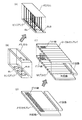
- the configuration of the MC and SA array 120, block 130 will be described with reference to FIG. 1B.
- the MC and SA array 120 has a structure in which the memory cell array 125 is stacked on the sense amplifier array 121.
- Sense amplifier array 121 has N 0 sense amplifier blocks 131, and memory cell array 125 has N 0 local cell arrays 135.
- the block 130 has a structure in which the local cell array 135 is stacked on the sense amplifier block 131.
- the local cell array 135 has a plurality of memory cells 20.
- the memory cell 20 has a transistor Tw1 and a capacitive element C1, and is electrically connected to the word line WL, the bit line BL (or BLB), the wiring BGL, and a power supply line for the voltage VSSS.
- the transistor Tw1 is an OS transistor having a back gate.
- the back gate is electrically connected to the wiring BGL.
- the voltage Vbg1 is input to the wiring BGL.
- the threshold voltage of the transistor Tw1 can be changed by the voltage Vbg1.
- a word line WL, bit lines BL and BLB, and a wiring BGL are provided in accordance with the arrangement of the memory cells 20.
- the OS transistor Since the band gap of the metal oxide is 2.5 eV or more, the OS transistor has a minimal off current. As an example, when the voltage between the source and the drain is 3.5 V at room temperature (25 ° C.), the off current per 1 ⁇ m of the channel width is less than 1 ⁇ 10 ⁇ 20 A, less than 1 ⁇ 10 ⁇ 22 A, or It can be less than 1 ⁇ 10 ⁇ 24 A. That is, the on / off current ratio of the drain current can be made to be 20 digits or more and 150 digits or less. Therefore, the memory cell 20 has a very small amount of charge leaking from the holding node via the transistor Tw1. Therefore, the DOSRAM 100 can be used as a non-volatile storage device.
- the metal oxide applied to the OS transistor is Zn oxide, Zn-Sn oxide, Ga-Sn oxide, In-Ga oxide, In-Zn oxide, In-M-Zn oxide (M is Ti, Ga, Y, Zr, La, Ce, Nd, Sn or Hf) and the like.
- oxides containing indium and zinc include aluminum, gallium, yttrium, copper, vanadium, beryllium, boron, silicon, titanium, iron, nickel, germanium, zirconium, molybdenum, lanthanum, cerium, neodymium, hafnium, tantalum, tungsten
- magnesium and the like may be included.
- the metal oxide applied to the semiconductor layer is preferably a metal oxide having a crystal part such as CAAC-OS, CAC-OS, or nc-OS.
- CAAC-OS is an abbreviation of c-axis-aligned crystalline metal oxide semiconductor.
- CAC-OS is an abbreviation of Cloud-Aligned Composite metal oxide semiconductor.
- nc-OS is an abbreviation of nanocrystalline metal oxide semiconductor.
- the CAAC-OS has c-axis orientation, and a plurality of nanocrystals are connected in the a-b plane direction to form a strained crystal structure.
- distortion shows the location where direction of the lattice arrangement
- the CAC-OS has a function of flowing electrons (or holes) serving as carriers and a function of not flowing electrons serving as carriers. By separating the function of flowing electrons and the function of not flowing electrons, both functions can be maximized. That is, by using CAC-OS in the channel formation region of the OS transistor, both high on current and extremely low off current can be realized. Thus, the OS transistor is very suitable for the write transistor of the memory cell.
- the sense amplifier block 131 is provided with a plurality of sense amplifiers 132.
- the sense amplifier 132 has a function of comparing voltages between the bit line BL and the bit line BLB, and a function of amplifying a voltage difference between the bit line BL and the bit line BLB.
- the two bit lines simultaneously compared by the sense amplifier 132 are referred to as a bit line pair.
- BL and BLB form a bit line pair. In this specification, it may be described as a bit line pair (BL, BLB).
- FIG. 2A shows a structural example of a bit line according to one embodiment of the present invention
- FIGS. 2B to 2D show comparative examples.
- the sense amplifier array and the memory cell array do not have a stacked structure, and the sense amplifier is provided in the column circuit. Therefore, in the comparative example of FIG. 2D, the bit lines have the same length as the memory cell array.
- the memory cell array is divided into a plurality of local cell arrays, and the local cell array is stacked on the sense amplifier block. Therefore, the length of the bit line provided in the local cell array can be shortened to the same length as the sense amplifier block.
- the number of memory cells per bit line hereinafter also referred to as CPB
- the CPB decreases. As the CPB is smaller, the bit line can be shortened, and hence the capacity (also referred to as bit line capacity) associated with the bit line is smaller.
- the capacitance Cs of the capacitive element C1 of the memory cell 20 can be reduced as in the conventional DRAM using a Si transistor, it is preferable in operating speed, power consumption, manufacturing yield and the like of the DOSRAM 100. Reducing the bit line capacitance leads to the reduction of capacitance Cs.
- the small capacitance Cs can simplify the structure of the capacitive element C1 and the manufacturing process thereof. Furthermore, miniaturization of the DOSRAM 100 or increase of the storage capacity is possible.
- FIG. 2B is an enlarged view of a part of the local cell array and the sense amplifier block of FIG. 2C.
- the bit line pair (BL, BLB) for connecting the sense amplifier and the memory cell can be both the local cell array and the sense amplifier block.
- BL, BLB bit line pair
- FIG. 2A in the local cell array, no bit line is routed.
- the main conduction portion between the memory cell and the sense amplifier is formed of a conductor provided in the via. That is, the bit line in the sense amplifier and the bit line in the local cell array are integrated.
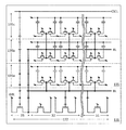
- FIG. 4 shows an example in which the CPB of the local cell array 135 is 8 and two pairs of bit lines (BL, BLB) are provided for the global bit line pair (GBL, GBLB).
- Signals EQ, EQB, SEN, SENB, and CSEL [3: 0] and a voltage Vpre are input to the sense amplifier block 131.
- Signals EQB and SENB are inverted signals of the signals EQ and SEN, respectively.
- the sense amplifier 132 has an equalizer 31, a sense amplifier 32, and a selector 33.
- Signals EQ and EQB are signals for activating the equalizer 31, and signals SEN and SENB are signals for activating the sense amplifier 32.
- the signals EQ, EQB, SEN, SENB are generated by the sense amplifier driver 114.
- sense amplifier driver 114 When local cell array 135 ⁇ j> (j is an integer from 0 to N 0 ⁇ 1) is to be accessed, sense amplifier block 131 ⁇ j> is active, and the other sense amplifier blocks 131 are inactive.
- the sense amplifier driver 114 generates signals EQ, EQB, SEN, and SENB. Such control can reduce the power consumption of the DOS RAM 100.
- the signal CSEL [3: 0] is generated by the column selector 113.
- One of four bit line pairs (BL, BLB) is made conductive to global bit line pair (GBL, GBLB) by signal CSEL [3: 0].
- global sense amplifier 140 is provided for each global bit line pair (GBL, GBLB).
- a write circuit 142 and a read circuit 143 are provided for each global bit line pair (GBL, GBLB).
- the write circuit 142 has a function of writing data to the global bit line pair (GBL, GBLB).
- the read circuit 143 has a function of holding data input to the global bit line pair (GBL, GBLB) and a function of outputting the held data.
- bit lines BL are drawn as being drawn around the sense amplifier block 131 and the local cell array 135, but as shown in FIG. 3A, the sense amplifier block 131 and the local cell array 135 are shown. Can be provided only in the local cell array 135.
- FIG. 3A corresponds to the circuit diagram of FIG. 2A.
- FIG. 3B shows a circuit diagram of FIG. 2B.
- the routing portion of the bit line BL is provided above the transistor Tw1.
- this routing portion is not provided in the local cell array 135.
- a portion shown by a dotted line represents a reduced portion of bit line BL.
- the length of the bit line BL in FIG. 3A is approximately half that in FIG. 3B.
- the bit line capacitance can be reduced by shortening the bit line.
- bit line capacitance Cbit
- Cs bit line capacitance
- the larger the Cs / Cbit the larger the voltage difference between the bit line pair obtained when data is read from the memory cell 20. Therefore, the larger the Cs / Cbit, the faster or more stable read operation can be realized.
- the capacitance Cs of the capacitive element C can be reduced by reducing the bit line capacitance Cbit. Therefore, when the capacitance value Cs of the capacitive element C1 is the same, the DOSRAM 100 has excellent read performance as compared to the conventional DRAM using a Si transistor.
- the DOSRAM 100 Since the transistor Tw1 is an OS transistor having a very small off-state current, the DOSRAM 100 has excellent retention characteristics as compared with the conventional DRAM even with a capacitance Cs smaller than that of the DRAM. Therefore, the DOSRAM 100 is preferable because the capacitance Cs of the capacitive element C1 can be made smaller.
- the local cell array 135 can have a multilayer structure.
- FIG. 5 shows an example in which the local cell array 135 is configured by the cell arrays 135a to 135c of three layers.
- the cell array 135b is provided with a routing portion of the bit line BL, and the transistor Tw1 of the cell array 135c is electrically connected to this routing portion.
- the sense amplifier 132 is shown as an example composed of a Si transistor, it may be composed of an OS transistor.
- NOSRAM Nonvolatile Oxide Semiconductor RAM
- a memory cell is configured by 2T type or 3T type gain cells, and a transistor of the memory cell is an OS transistor.
- the memory cell 22 illustrated in FIG. 6 includes three transistors Tw2, Tr2, and Ts2.
- the transistors Tw2, Tr2, and Ts2 are OS transistors having a back gate.
- the memory cell 22 may be provided with a capacitive element for holding the gate voltage of the transistor Tr2.
- the memory cell 22 is electrically connected to the write word line WWL, the read word RWL, the write bit line WBL, the read bit line RBL, and the source line SL.
- the write bit line WBL and the read bit line RBL are electrically connected to the sense amplifier.
- the structure of the bit line of this embodiment can be applied to one or both of the write bit line WBL and the read bit line RBL.
- the structure of the bit line disclosed in this embodiment can be applied to a semiconductor device formed by stacking transistors. By shortening the wiring, the parasitic capacitance of the wiring is reduced, which leads to the improvement of the performance of the semiconductor device.
- the above-described oxide semiconductor memory device can be incorporated into various processor chips such as a CPU chip, a GPU chip, an FPGA chip, and an application processor (AP) chip.
- processor chips such as a CPU chip, a GPU chip, an FPGA chip, and an application processor (AP) chip.
- AP application processor
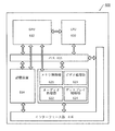
- the AP chip 600 illustrated in FIG. 7 includes a CPU (central processing unit) 610, a GPU (graphics computing unit) 612, a storage unit 614, a bus 615, an interface unit 616, a memory control unit 621, an audio processing unit 622, and a video processing unit 623. , And a display control unit 624. These integrated circuits are provided on one die. The circuits provided in the AP chip 600 are appropriately discarded depending on the application and the like. The above oxide semiconductor memory device is used for the memory device 614.
- the AP chip 600 can control various peripheral devices.
- the memory control unit 621 is provided with a memory controller, a controller for DRAM, and a controller for flash memory.
- the audio processing unit 622 processes audio data and the like.
- the video processing unit 623 is provided with a video decoder, a video encoder, an image processing circuit for a camera, and the like.
- the display control unit 624 is provided with a display controller and a multi-monitor controller.
- the memory chip 630 including the above-described oxide semiconductor memory device and the processor chip 640 incorporating the above-described oxide semiconductor memory device can be incorporated into various electronic devices.
- the memory chip 630 can be replaced with a DRAM chip or a flash memory chip.
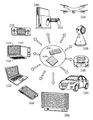
- FIG. 8 illustrates some electronic devices in which memory chip 630 and / or processor chip 640 are incorporated.
- the robot 7100 includes an illuminance sensor, a microphone, a camera, a speaker, a display, various sensors (an infrared sensor, an ultrasonic sensor, an acceleration sensor, a piezo sensor, an optical sensor, a gyro sensor, and the like), a moving mechanism, and the like.
- the processor chip 640 controls these peripherals.
- the memory chip 630 stores data acquired by the sensor.
- the microphone has a function of detecting an acoustic signal such as a user's voice and an environmental sound.
- the speaker has a function of emitting audio signals such as voice and warning sound.
- the robot 7100 can analyze an audio signal input through a microphone and emit a necessary audio signal from a speaker.
- the robot 7100 can communicate with a user using a microphone and a speaker.
- the camera has a function of imaging the periphery of the robot 7100.
- the robot 7100 has a function of moving using a moving mechanism.
- the robot 7100 can capture an image of the surroundings using a camera and analyze the image to detect the presence or absence of an obstacle when moving.
- a flying object 7120 has a propeller, a camera, a battery, and the like, and has a function to fly autonomously.
- the processor chip 640 controls these peripherals.
- image data captured by a camera is stored in the memory chip 630.
- the processor chip 640 may analyze image data to detect the presence or absence of an obstacle during movement. Further, the remaining battery capacity can be estimated by the processor chip 640 from the change in the storage capacity of the battery.
- the cleaning robot 7140 has a display disposed on the top, a plurality of cameras disposed on the side, brushes, operation buttons, various sensors, and the like. Although not shown, the cleaning robot 7140 is provided with a tire, a suction port and the like. The cleaning robot 7140 can self-propelled, detect dust, and suction dust from a suction port provided on the lower surface.
- the processor chip 640 may analyze the image captured by the camera to determine the presence or absence of an obstacle, such as a wall, furniture or steps.
- an obstacle such as a wall, furniture or steps.
- the rotation of the brush can be stopped.
- the automobile 7160 has an engine, tires, brakes, a steering device, a camera and the like.
- the processor chip 640 performs control for optimizing the traveling state of the automobile 7160 based on data such as navigation information, speed, engine state, gear selection state, and brake use frequency.
- image data captured by a camera is stored in the memory chip 630.
- the memory chip 630 and / or the processor chip 640 can be incorporated in a TV (television receiver) device 7200, a smartphone 7210, a PC (personal computer) 7220, 7230, a game machine 7240, 7260 or the like.
- a processor chip 640 incorporated in the TV set 7200 can function as an image engine.
- the processor chip 640 performs image processing such as noise removal and resolution upconversion.
- the smartphone 7210 is an example of a portable information terminal.
- the smartphone 7210 includes a microphone, a camera, a speaker, various sensors, and a display portion.
- the processor chip 640 controls these peripherals.
- the PCs 7220 and 7230 are examples of a notebook PC and a stationary PC, respectively.
- a keyboard 7232 and a monitor device 7233 can be connected to the PC 7230 wirelessly or by wire.
- the game machine 7240 is an example of a portable game machine.
- the game machine 7260 is an example of a stationary game machine.
- a controller 7262 is connected to the game machine 7260 wirelessly or by wire. Memory chip 630 and / or processor chip 640 may also be incorporated into controller 7262.
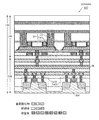
- FIG. 9 shows a cross section of a representative block 130. As described above, in block 130, the local cell array 135 is stacked on the sense amplifier block 131. 9 corresponds to the cross-sectional view of the circuit diagram of FIG. 3A.
- the sense amplifier block 131 is provided with a bit line BL and Si transistors Ta10 and Ta11.
- the Si transistors Ta10 and Ta11 have a semiconductor layer on a single crystal silicon wafer.
- the Si transistors Ta10 and Ta11 constitute a sense amplifier 132 and are electrically connected to the bit line BL.
- the two transistors Tw1 share a semiconductor layer.
- a plurality of conductors are stacked between the semiconductor layer and the bit line BL.
- the transistor Tw1 is conducted to the bit line BL by these conductors.
- Such a connection structure allows sense amplifier block 131 and local cell array 135 to share bit line BL in local cell array 135.
- the memory cell 20 can be configured by the capacitive element C1 having a small capacitance Cs.
- the capacitive element C1 may have a structure as shown in FIG. By reducing the area of the capacitive element C1, the area of the memory cell 20 can be reduced, and the DOSRAM 100 can be miniaturized.
- connection structure of the semiconductor layer and the wiring as illustrated in FIGS. 9 and 10 can be applied to various semiconductor devices configured by stacking a plurality of circuits each including a transistor group.
- the metal oxide, the insulator, the conductor, and the like in FIGS. 9 and 10 may be a single layer or a stack.
- Various film forming methods such as sputtering method, molecular beam epitaxy method (MBE method), pulse laser ablation method (PLA method), CVD method, atomic layer deposition method (ALD method), etc. can be used for these fabrications.
- the CVD method includes a plasma CVD method, a thermal CVD method, an organic metal CVD method and the like.
- the semiconductor layer of the transistor Tw1 is formed of three metal oxide layers. These metal oxide layers are preferably made of the above-described metal oxides, and more preferably made of a metal oxide containing In, Ga, and Zn.
- the metal oxide may increase the carrier density and reduce resistance by adding an element that forms an oxygen vacancy or an element that bonds to the oxygen vacancy. For example, by selectively reducing the resistance of the semiconductor layer using a metal oxide, the source region and the drain region can be provided in the semiconductor layer.
- boron or phosphorus is typically mentioned.
- hydrogen, carbon, nitrogen, fluorine, sulfur, chlorine, titanium, a rare gas or the like may be used.
- noble gases are helium, neon, argon, krypton and xenon.
- the resistance of the semiconductor layer can be selectively reduced by using a dummy gate.
- a dummy gate is provided over the semiconductor layer with the insulating layer interposed therebetween, and the above-described elements are added to the semiconductor layer using the dummy gate as a mask. Therefore, the element is added to a region of the semiconductor layer which is not overlapped with the dummy gate, and the resistance is lowered.
- the element can be added by an ion implantation method in which the ionized source gas is separated by mass separation, an ion doping method in which the ionized source gas is added without mass separation, or a plasma immersion ion implantation method.
- the conductive material used for the conductor includes a semiconductor typified by polycrystalline silicon doped with an impurity element such as phosphorus, a silicide such as nickel silicide, molybdenum, titanium, tantalum, tungsten, aluminum, copper, chromium, neodymium, scandium And metal nitrides (tantalum nitride, titanium nitride, molybdenum nitride, tungsten nitride) or the like containing the above-described metal as a component.
- an impurity element such as phosphorus
- a silicide such as nickel silicide, molybdenum, titanium, tantalum, tungsten, aluminum, copper, chromium, neodymium, scandium And metal nitrides (tantalum nitride, titanium nitride, molybdenum nitride, tungsten nitride) or the like containing the above-described
- indium tin oxide indium oxide containing tungsten oxide, indium zinc oxide containing tungsten oxide, indium oxide containing titanium oxide, indium tin oxide containing titanium oxide, indium zinc oxide, silicon oxide are added.
- Conductive materials such as indium tin oxide can be used.
- the insulating materials used for the insulator include aluminum nitride, aluminum oxide, aluminum nitride oxide, aluminum oxynitride, magnesium oxide, silicon oxide, silicon oxide, silicon nitride oxide, silicon oxynitride, gallium oxide, germanium oxide, yttrium oxide, There are zirconium oxide, lanthanum oxide, neodymium oxide, hafnium oxide, tantalum oxide, aluminum silicate and the like.
- oxynitride refers to a compound in which the content of oxygen is higher than nitrogen
- nitrided oxide refers to a compound in which the content of nitrogen is higher than oxygen.
Landscapes
- Engineering & Computer Science (AREA)
- Microelectronics & Electronic Packaging (AREA)
- Computer Hardware Design (AREA)
- Semiconductor Memories (AREA)
- Thin Film Transistor (AREA)
- Non-Volatile Memory (AREA)
- Dram (AREA)
Abstract
Description
本実施の形態では、酸化物半導体記憶装置の一例として、DOSRAM(登録商標)について説明する。なお、「DOSRAM」の名称は、Dynamic Oxide Semiconductor Random Access Memoryに由来する。“DOSRAM”とは、メモリセルが、1T1C(1トランジスタ1容量)型セルであり、かつ書込みトランジスタがOSトランジスタである記憶装置のことである。
図1は、DOSRAMの構成例を示す機能ブロック図である。図1に示すDOSRAM100は、制御回路102、行回路104、列回路105、メモリセル(MC)及びセンスアンプ(SA)アレイ120を有する。行回路104はデコーダ111、ワード線ドライバ112、列セレクタ113、センスアンプドライバ114を有する。列回路105はグローバルセンスアンプブロック115、入出力(I/O)回路116を有する。
本実施の形態では、上掲の酸化物半導体記憶装置を有する電子部品、電子機器等について説明する。
本実施の形態では、DOSRAM100の積層構造例について説明する。図9は、代表的なブロック130の断面を示している。上掲したように、ブロック130において、センスアンプブロック131にローカルセルアレイ135が積層されている。なお、図9は、図3Aの回路図の断面図に対応する。
Claims (9)
- 第1配線および第1トランジスタが設けられている第1回路と、
第2トランジスタが設けられている第2回路と、
を有する半導体装置であり、
前記第2回路は前記第1回路上に積層され、
前記第1トランジスタと前記第2トランジスタとは前記第1配線に電気的に接続され、
前記第2回路には、前記第1配線の引き回し部が設けられていないことを特徴とする半導体装置。 - 第1回路および第2回路を有する半導体装置であり、
前記第1回路は、
第1トランジスタと、
前記第1トランジスタに電気的に接続されている第1配線とを有し、
前記第2回路は、
導電体と、
前記導電体を介して、前記第1配線に電気的に接続されている第2トランジスタとを有し、
前記導電体は、前記第2トランジスタの半導体層の下面に接する部分を有することを特徴とする半導体装置。 - 請求項1または2において、
前記第2トランジスタの半導体層は、金属酸化物を有することを特徴とする半導体装置。 - 請求項1または2において、
前記第1トランジスタおよび前記第2トランジスタの半導体層は、金属酸化物を有することを特徴とする半導体装置。 - ビット線と、
前記ビット線に電気的に接続されているセンスアンプと、
前記センスアンプ上に積層されているメモリセルアレイと、
を有する記憶装置であって、
前記メモリセルアレイは、前記ビット線に電気的に接続されているメモリセルを有し、
前記メモリセルは、前記ビット線に電気的に接続されている書込みトランジスタと、前記書込みトランジスタに電気的に接続されている容量素子とを有し、
前記メモリセルアレイ内には、前記ビット線の引き回し部分が存在しないことを特徴とする記憶装置。 - 請求項5において、
前記書込みトランジスタの半導体層は、金属酸化物を有することを特徴とする記憶装置。 - センスアンプブロックと、
前記センスアンプブロック上に積層されているメモリセルアレイとを有する記憶装置であって、
前記センスアンプブロックは、
ビット線と、
前記ビット線に電気的に接続されているセンスアンプとを有し、
前記メモリセルアレイは、導電体と、メモリセルとを有し、
前記メモリセルは、
前記導電体を介して前記ビット線に電気的に接続されている書込みトランジスタと、
前記書込みトランジスタに電気的に接続されている容量素子とを有し、
前記導電体は、前記書込みトランジスタの半導体層の下面に接する部分を有することを特徴とする記憶装置。 - 請求項7において、
前記書込みトランジスタの前記半導体層は、金属酸化物を有することを特徴とする記憶装置。 - 請求項5乃至8の何れか1項に記載の記憶装置が組み込まれている電子機器。
Priority Applications (6)
| Application Number | Priority Date | Filing Date | Title |
|---|---|---|---|
| JP2019540723A JP7328146B2 (ja) | 2017-09-06 | 2018-08-24 | 記憶装置及び電子機器 |
| CN201880058030.4A CN111052350B (zh) | 2017-09-06 | 2018-08-24 | 半导体装置、存储装置及电子设备 |
| KR1020207005187A KR102707746B1 (ko) | 2017-09-06 | 2018-08-24 | 반도체 장치, 기억 장치, 및 전자 기기 |
| US16/640,206 US11074962B2 (en) | 2017-09-06 | 2018-08-27 | Semiconductor device, memory device, and electronic device |
| US17/377,757 US11657867B2 (en) | 2017-09-06 | 2021-07-16 | Semiconductor device, memory device, and electronic device |
| US18/135,779 US12230314B2 (en) | 2017-09-06 | 2023-04-18 | Semiconductor device, memory device, and electronic device |
Applications Claiming Priority (4)
| Application Number | Priority Date | Filing Date | Title |
|---|---|---|---|
| JP2017-170814 | 2017-09-06 | ||
| JP2017170814 | 2017-09-06 | ||
| JP2018034610 | 2018-02-28 | ||
| JP2018-034610 | 2018-02-28 |
Related Child Applications (2)
| Application Number | Title | Priority Date | Filing Date |
|---|---|---|---|
| US16/640,206 A-371-Of-International US11074962B2 (en) | 2017-09-06 | 2018-08-27 | Semiconductor device, memory device, and electronic device |
| US17/377,757 Continuation US11657867B2 (en) | 2017-09-06 | 2021-07-16 | Semiconductor device, memory device, and electronic device |
Publications (1)
| Publication Number | Publication Date |
|---|---|
| WO2019048967A1 true WO2019048967A1 (ja) | 2019-03-14 |
Family
ID=65633620
Family Applications (1)
| Application Number | Title | Priority Date | Filing Date |
|---|---|---|---|
| PCT/IB2018/056412 Ceased WO2019048967A1 (ja) | 2017-09-06 | 2018-08-24 | 半導体装置、記憶装置、及び電子機器 |
Country Status (5)
| Country | Link |
|---|---|
| US (3) | US11074962B2 (ja) |
| JP (1) | JP7328146B2 (ja) |
| KR (1) | KR102707746B1 (ja) |
| CN (1) | CN111052350B (ja) |
| WO (1) | WO2019048967A1 (ja) |
Cited By (4)
| Publication number | Priority date | Publication date | Assignee | Title |
|---|---|---|---|---|
| WO2020201865A1 (ja) * | 2019-03-29 | 2020-10-08 | 株式会社半導体エネルギー研究所 | 半導体装置 |
| JPWO2020234689A1 (ja) * | 2019-05-23 | 2020-11-26 | ||
| US11094360B2 (en) | 2017-10-13 | 2021-08-17 | Semiconductor Energy Laboratory Co., Ltd. | Storage device, electronic component, and electronic device |
| JP2024167372A (ja) * | 2019-07-12 | 2024-12-03 | 株式会社半導体エネルギー研究所 | 半導体装置 |
Families Citing this family (3)
| Publication number | Priority date | Publication date | Assignee | Title |
|---|---|---|---|---|
| US12205892B2 (en) | 2018-12-27 | 2025-01-21 | Semiconductor Energy Laboratory Co., Ltd. | Semiconductor device |
| US11690212B2 (en) * | 2019-06-28 | 2023-06-27 | Intel Corporation | Memory architecture at back-end-of-line |
| CN113451270B (zh) * | 2020-03-25 | 2023-12-05 | 长鑫存储技术有限公司 | 位线结构和半导体存储器 |
Citations (5)
| Publication number | Priority date | Publication date | Assignee | Title |
|---|---|---|---|---|
| JP2013065638A (ja) * | 2011-09-15 | 2013-04-11 | Elpida Memory Inc | 半導体装置 |
| JP2015084411A (ja) * | 2013-09-18 | 2015-04-30 | 株式会社半導体エネルギー研究所 | 半導体装置及びその作製方法 |
| JP2015187905A (ja) * | 2014-03-13 | 2015-10-29 | 株式会社半導体エネルギー研究所 | 半導体装置 |
| JP2015228492A (ja) * | 2014-05-09 | 2015-12-17 | 株式会社半導体エネルギー研究所 | 記憶装置及び電子機器 |
| JP2016212944A (ja) * | 2015-05-11 | 2016-12-15 | 株式会社半導体エネルギー研究所 | 半導体装置、又は該半導体装置を有する電子部品 |
Family Cites Families (18)
| Publication number | Priority date | Publication date | Assignee | Title |
|---|---|---|---|---|
| JP3603229B2 (ja) * | 1994-02-09 | 2004-12-22 | 富士通株式会社 | 半導体記憶装置 |
| JP2010192718A (ja) * | 2009-02-19 | 2010-09-02 | Toshiba Corp | 不揮発性半導体記憶装置及びその製造方法 |
| WO2012029638A1 (en) | 2010-09-03 | 2012-03-08 | Semiconductor Energy Laboratory Co., Ltd. | Semiconductor device |
| JP2012256821A (ja) * | 2010-09-13 | 2012-12-27 | Semiconductor Energy Lab Co Ltd | 記憶装置 |
| TWI539453B (zh) | 2010-09-14 | 2016-06-21 | 半導體能源研究所股份有限公司 | 記憶體裝置和半導體裝置 |
| JP5996850B2 (ja) * | 2010-10-12 | 2016-09-21 | 日東電工株式会社 | 回路付サスペンション基板およびその製造方法 |
| TWI520273B (zh) * | 2011-02-02 | 2016-02-01 | 半導體能源研究所股份有限公司 | 半導體儲存裝置 |
| JP6105266B2 (ja) * | 2011-12-15 | 2017-03-29 | 株式会社半導体エネルギー研究所 | 記憶装置 |
| JP2014170599A (ja) * | 2013-03-01 | 2014-09-18 | Toshiba Corp | 半導体記憶装置 |
| JP6405100B2 (ja) * | 2013-03-08 | 2018-10-17 | 株式会社半導体エネルギー研究所 | 半導体装置 |
| TWI767772B (zh) * | 2014-04-10 | 2022-06-11 | 日商半導體能源研究所股份有限公司 | 記憶體裝置及半導體裝置 |
| KR20170069207A (ko) * | 2014-10-10 | 2017-06-20 | 가부시키가이샤 한도오따이 에네루기 켄큐쇼 | 반도체 장치, 회로 기판, 및 전자 기기 |
| US9583177B2 (en) * | 2014-12-10 | 2017-02-28 | Semiconductor Energy Laboratory Co., Ltd. | Memory device and semiconductor device including memory device |
| WO2016092416A1 (en) * | 2014-12-11 | 2016-06-16 | Semiconductor Energy Laboratory Co., Ltd. | Semiconductor device, memory device, and electronic device |
| US9589611B2 (en) * | 2015-04-01 | 2017-03-07 | Semiconductor Energy Laboratory Co., Ltd. | Memory device, semiconductor device, and electronic device |
| US9627034B2 (en) * | 2015-05-15 | 2017-04-18 | Semiconductor Energy Laboratory Co., Ltd. | Electronic device |
| JP2017120833A (ja) * | 2015-12-28 | 2017-07-06 | 株式会社半導体エネルギー研究所 | 半導体装置およびその作製方法、半導体基板、回路基板ならびに電子機器 |
| JP7358079B2 (ja) * | 2019-06-10 | 2023-10-10 | キヤノン株式会社 | 撮像装置、撮像システムおよび半導体チップ |
-
2018
- 2018-08-24 JP JP2019540723A patent/JP7328146B2/ja active Active
- 2018-08-24 WO PCT/IB2018/056412 patent/WO2019048967A1/ja not_active Ceased
- 2018-08-24 CN CN201880058030.4A patent/CN111052350B/zh active Active
- 2018-08-24 KR KR1020207005187A patent/KR102707746B1/ko active Active
- 2018-08-27 US US16/640,206 patent/US11074962B2/en active Active
-
2021
- 2021-07-16 US US17/377,757 patent/US11657867B2/en active Active
-
2023
- 2023-04-18 US US18/135,779 patent/US12230314B2/en active Active
Patent Citations (5)
| Publication number | Priority date | Publication date | Assignee | Title |
|---|---|---|---|---|
| JP2013065638A (ja) * | 2011-09-15 | 2013-04-11 | Elpida Memory Inc | 半導体装置 |
| JP2015084411A (ja) * | 2013-09-18 | 2015-04-30 | 株式会社半導体エネルギー研究所 | 半導体装置及びその作製方法 |
| JP2015187905A (ja) * | 2014-03-13 | 2015-10-29 | 株式会社半導体エネルギー研究所 | 半導体装置 |
| JP2015228492A (ja) * | 2014-05-09 | 2015-12-17 | 株式会社半導体エネルギー研究所 | 記憶装置及び電子機器 |
| JP2016212944A (ja) * | 2015-05-11 | 2016-12-15 | 株式会社半導体エネルギー研究所 | 半導体装置、又は該半導体装置を有する電子部品 |
Cited By (14)
| Publication number | Priority date | Publication date | Assignee | Title |
|---|---|---|---|---|
| US11922987B2 (en) | 2017-10-13 | 2024-03-05 | Semiconductor Energy Laboratory Co., Ltd. | Storage device, electronic component, and electronic device |
| US11094360B2 (en) | 2017-10-13 | 2021-08-17 | Semiconductor Energy Laboratory Co., Ltd. | Storage device, electronic component, and electronic device |
| US11532340B2 (en) | 2017-10-13 | 2022-12-20 | Semiconductor Energy Laboratory Co., Ltd. | Storage device, electronic component, and electronic device |
| US12531114B2 (en) | 2019-03-29 | 2026-01-20 | Semiconductor Energy Laboratory Co., Ltd. | Semiconductor device |
| US11948626B2 (en) | 2019-03-29 | 2024-04-02 | Semiconductor Energy Laboratory Co., Ltd. | Semiconductor device comprising transistors with silicon and metal oxide channels |
| WO2020201865A1 (ja) * | 2019-03-29 | 2020-10-08 | 株式会社半導体エネルギー研究所 | 半導体装置 |
| WO2020234689A1 (ja) * | 2019-05-23 | 2020-11-26 | 株式会社半導体エネルギー研究所 | 半導体装置 |
| US11869627B2 (en) | 2019-05-23 | 2024-01-09 | Semiconductor Energy Laboratory Co., Ltd. | Semiconductor device comprising memory circuit over control circuits |
| JPWO2020234689A1 (ja) * | 2019-05-23 | 2020-11-26 | ||
| JP2024079742A (ja) * | 2019-05-23 | 2024-06-11 | 株式会社半導体エネルギー研究所 | 半導体装置 |
| JP7639207B2 (ja) | 2019-05-23 | 2025-03-04 | 株式会社半導体エネルギー研究所 | 半導体装置 |
| JP7459079B2 (ja) | 2019-05-23 | 2024-04-01 | 株式会社半導体エネルギー研究所 | 半導体装置 |
| KR102931352B1 (ko) | 2019-05-23 | 2026-02-27 | 가부시키가이샤 한도오따이 에네루기 켄큐쇼 | 반도체 장치 |
| JP2024167372A (ja) * | 2019-07-12 | 2024-12-03 | 株式会社半導体エネルギー研究所 | 半導体装置 |
Also Published As
| Publication number | Publication date |
|---|---|
| US20210343329A1 (en) | 2021-11-04 |
| US20230253031A1 (en) | 2023-08-10 |
| JPWO2019048967A1 (ja) | 2020-10-29 |
| CN111052350B (zh) | 2024-04-26 |
| KR102707746B1 (ko) | 2024-09-19 |
| US12230314B2 (en) | 2025-02-18 |
| US11074962B2 (en) | 2021-07-27 |
| KR20200050955A (ko) | 2020-05-12 |
| JP7328146B2 (ja) | 2023-08-16 |
| US11657867B2 (en) | 2023-05-23 |
| US20200185023A1 (en) | 2020-06-11 |
| CN111052350A (zh) | 2020-04-21 |
Similar Documents
| Publication | Publication Date | Title |
|---|---|---|
| JP7328146B2 (ja) | 記憶装置及び電子機器 | |
| US11062762B2 (en) | Storage device applying a cancel circuit | |
| TWI794834B (zh) | 比較電路、半導體裝置、電子元件及電子裝置 | |
| JP6866232B2 (ja) | 半導体装置、電子部品、および電子機器 | |
| US11699465B2 (en) | Memory device | |
| JP2020038977A (ja) | 記憶装置 | |
| JP2025098163A (ja) | 半導体装置 | |
| TW201812767A (zh) | 記憶體裝置及其驅動方法、半導體裝置、電子構件以及電子裝置 | |
| TW202537448A (zh) | 半導體裝置及包括該半導體裝置的電子裝置 | |
| JP2017224377A (ja) | メモリ装置、およびそれを有する半導体装置 | |
| JP2022003572A (ja) | 半導体装置 | |
| TWI724231B (zh) | 記憶體裝置及其工作方法、半導體裝置、電子構件以及電子裝置 | |
| WO2020234689A1 (ja) | 半導体装置 | |
| CN112041825A (zh) | 半导体装置 | |
| WO2018220471A1 (ja) | 記憶装置及びその動作方法 | |
| JP7225349B2 (ja) | 記憶装置 | |
| JP2019016681A (ja) | 記憶装置 |
Legal Events
| Date | Code | Title | Description |
|---|---|---|---|
| 121 | Ep: the epo has been informed by wipo that ep was designated in this application |
Ref document number: 18854206 Country of ref document: EP Kind code of ref document: A1 |
|
| ENP | Entry into the national phase |
Ref document number: 20207005187 Country of ref document: KR Kind code of ref document: A |
|
| ENP | Entry into the national phase |
Ref document number: 2019540723 Country of ref document: JP Kind code of ref document: A |
|
| NENP | Non-entry into the national phase |
Ref country code: DE |
|
| 122 | Ep: pct application non-entry in european phase |
Ref document number: 18854206 Country of ref document: EP Kind code of ref document: A1 |