WO2019038876A1 - 半導体装置 - Google Patents
半導体装置 Download PDFInfo
- Publication number
- WO2019038876A1 WO2019038876A1 PCT/JP2017/030280 JP2017030280W WO2019038876A1 WO 2019038876 A1 WO2019038876 A1 WO 2019038876A1 JP 2017030280 W JP2017030280 W JP 2017030280W WO 2019038876 A1 WO2019038876 A1 WO 2019038876A1
- Authority
- WO
- WIPO (PCT)
- Prior art keywords
- semiconductor device
- heat
- electrically connected
- inner lead
- exposed
- Prior art date
- Legal status (The legal status is an assumption and is not a legal conclusion. Google has not performed a legal analysis and makes no representation as to the accuracy of the status listed.)
- Ceased
Links
Images



Classifications
-
- H—ELECTRICITY
- H10—SEMICONDUCTOR DEVICES; ELECTRIC SOLID-STATE DEVICES NOT OTHERWISE PROVIDED FOR
- H10W—GENERIC PACKAGES, INTERCONNECTIONS, CONNECTORS OR OTHER CONSTRUCTIONAL DETAILS OF DEVICES COVERED BY CLASS H10
- H10W40/00—Arrangements for thermal protection or thermal control
- H10W40/20—Arrangements for cooling
- H10W40/22—Arrangements for cooling characterised by their shape, e.g. having conical or cylindrical projections
-
- H—ELECTRICITY
- H10—SEMICONDUCTOR DEVICES; ELECTRIC SOLID-STATE DEVICES NOT OTHERWISE PROVIDED FOR
- H10W—GENERIC PACKAGES, INTERCONNECTIONS, CONNECTORS OR OTHER CONSTRUCTIONAL DETAILS OF DEVICES COVERED BY CLASS H10
- H10W72/00—Interconnections or connectors in packages
- H10W72/20—Bump connectors, e.g. solder bumps or copper pillars; Dummy bumps; Thermal bumps
-
- H—ELECTRICITY
- H10—SEMICONDUCTOR DEVICES; ELECTRIC SOLID-STATE DEVICES NOT OTHERWISE PROVIDED FOR
- H10W—GENERIC PACKAGES, INTERCONNECTIONS, CONNECTORS OR OTHER CONSTRUCTIONAL DETAILS OF DEVICES COVERED BY CLASS H10
- H10W70/00—Package substrates; Interposers; Redistribution layers [RDL]
- H10W70/40—Leadframes
- H10W70/464—Additional interconnections in combination with leadframes
- H10W70/468—Circuit boards
-
- H—ELECTRICITY
- H10—SEMICONDUCTOR DEVICES; ELECTRIC SOLID-STATE DEVICES NOT OTHERWISE PROVIDED FOR
- H10W—GENERIC PACKAGES, INTERCONNECTIONS, CONNECTORS OR OTHER CONSTRUCTIONAL DETAILS OF DEVICES COVERED BY CLASS H10
- H10W70/00—Package substrates; Interposers; Redistribution layers [RDL]
- H10W70/40—Leadframes
- H10W70/411—Chip-supporting parts, e.g. die pads
- H10W70/413—Insulating or insulated substrates serving as die pads
-
- H—ELECTRICITY
- H10—SEMICONDUCTOR DEVICES; ELECTRIC SOLID-STATE DEVICES NOT OTHERWISE PROVIDED FOR
- H10W—GENERIC PACKAGES, INTERCONNECTIONS, CONNECTORS OR OTHER CONSTRUCTIONAL DETAILS OF DEVICES COVERED BY CLASS H10
- H10W70/00—Package substrates; Interposers; Redistribution layers [RDL]
- H10W70/40—Leadframes
- H10W70/421—Shapes or dispositions
-
- H—ELECTRICITY
- H10—SEMICONDUCTOR DEVICES; ELECTRIC SOLID-STATE DEVICES NOT OTHERWISE PROVIDED FOR
- H10W—GENERIC PACKAGES, INTERCONNECTIONS, CONNECTORS OR OTHER CONSTRUCTIONAL DETAILS OF DEVICES COVERED BY CLASS H10
- H10W70/00—Package substrates; Interposers; Redistribution layers [RDL]
- H10W70/40—Leadframes
- H10W70/421—Shapes or dispositions
- H10W70/424—Cross-sectional shapes
-
- H—ELECTRICITY
- H10—SEMICONDUCTOR DEVICES; ELECTRIC SOLID-STATE DEVICES NOT OTHERWISE PROVIDED FOR
- H10W—GENERIC PACKAGES, INTERCONNECTIONS, CONNECTORS OR OTHER CONSTRUCTIONAL DETAILS OF DEVICES COVERED BY CLASS H10
- H10W70/00—Package substrates; Interposers; Redistribution layers [RDL]
- H10W70/40—Leadframes
- H10W70/464—Additional interconnections in combination with leadframes
- H10W70/465—Bumps or wires
-
- H—ELECTRICITY
- H10—SEMICONDUCTOR DEVICES; ELECTRIC SOLID-STATE DEVICES NOT OTHERWISE PROVIDED FOR
- H10W—GENERIC PACKAGES, INTERCONNECTIONS, CONNECTORS OR OTHER CONSTRUCTIONAL DETAILS OF DEVICES COVERED BY CLASS H10
- H10W70/00—Package substrates; Interposers; Redistribution layers [RDL]
- H10W70/40—Leadframes
- H10W70/464—Additional interconnections in combination with leadframes
- H10W70/466—Tape carriers or flat leads
-
- H—ELECTRICITY
- H10—SEMICONDUCTOR DEVICES; ELECTRIC SOLID-STATE DEVICES NOT OTHERWISE PROVIDED FOR
- H10W—GENERIC PACKAGES, INTERCONNECTIONS, CONNECTORS OR OTHER CONSTRUCTIONAL DETAILS OF DEVICES COVERED BY CLASS H10
- H10W70/00—Package substrates; Interposers; Redistribution layers [RDL]
- H10W70/40—Leadframes
- H10W70/479—Leadframes on or in insulating or insulated package substrates, interposers, or redistribution layers
-
- H—ELECTRICITY
- H10—SEMICONDUCTOR DEVICES; ELECTRIC SOLID-STATE DEVICES NOT OTHERWISE PROVIDED FOR
- H10W—GENERIC PACKAGES, INTERCONNECTIONS, CONNECTORS OR OTHER CONSTRUCTIONAL DETAILS OF DEVICES COVERED BY CLASS H10
- H10W74/00—Encapsulations, e.g. protective coatings
- H10W74/10—Encapsulations, e.g. protective coatings characterised by their shape or disposition
- H10W74/111—Encapsulations, e.g. protective coatings characterised by their shape or disposition the semiconductor body being completely enclosed
-
- H—ELECTRICITY
- H10—SEMICONDUCTOR DEVICES; ELECTRIC SOLID-STATE DEVICES NOT OTHERWISE PROVIDED FOR
- H10W—GENERIC PACKAGES, INTERCONNECTIONS, CONNECTORS OR OTHER CONSTRUCTIONAL DETAILS OF DEVICES COVERED BY CLASS H10
- H10W74/00—Encapsulations, e.g. protective coatings
- H10W74/10—Encapsulations, e.g. protective coatings characterised by their shape or disposition
- H10W74/111—Encapsulations, e.g. protective coatings characterised by their shape or disposition the semiconductor body being completely enclosed
- H10W74/114—Encapsulations, e.g. protective coatings characterised by their shape or disposition the semiconductor body being completely enclosed by a substrate and the encapsulations
-
- H—ELECTRICITY
- H10—SEMICONDUCTOR DEVICES; ELECTRIC SOLID-STATE DEVICES NOT OTHERWISE PROVIDED FOR
- H10W—GENERIC PACKAGES, INTERCONNECTIONS, CONNECTORS OR OTHER CONSTRUCTIONAL DETAILS OF DEVICES COVERED BY CLASS H10
- H10W90/00—Package configurations
- H10W90/701—Package configurations characterised by the relative positions of pads or connectors relative to package parts
-
- H—ELECTRICITY
- H10—SEMICONDUCTOR DEVICES; ELECTRIC SOLID-STATE DEVICES NOT OTHERWISE PROVIDED FOR
- H10W—GENERIC PACKAGES, INTERCONNECTIONS, CONNECTORS OR OTHER CONSTRUCTIONAL DETAILS OF DEVICES COVERED BY CLASS H10
- H10W70/00—Package substrates; Interposers; Redistribution layers [RDL]
- H10W70/40—Leadframes
- H10W70/421—Shapes or dispositions
- H10W70/424—Cross-sectional shapes
- H10W70/427—Bent parts
- H10W70/429—Bent parts being the outer leads
-
- H—ELECTRICITY
- H10—SEMICONDUCTOR DEVICES; ELECTRIC SOLID-STATE DEVICES NOT OTHERWISE PROVIDED FOR
- H10W—GENERIC PACKAGES, INTERCONNECTIONS, CONNECTORS OR OTHER CONSTRUCTIONAL DETAILS OF DEVICES COVERED BY CLASS H10
- H10W72/00—Interconnections or connectors in packages
- H10W72/071—Connecting or disconnecting
- H10W72/075—Connecting or disconnecting of bond wires
- H10W72/07551—Connecting or disconnecting of bond wires characterised by changes in properties of the bond wires during the connecting
- H10W72/07552—Connecting or disconnecting of bond wires characterised by changes in properties of the bond wires during the connecting changes in structures or sizes
-
- H—ELECTRICITY
- H10—SEMICONDUCTOR DEVICES; ELECTRIC SOLID-STATE DEVICES NOT OTHERWISE PROVIDED FOR
- H10W—GENERIC PACKAGES, INTERCONNECTIONS, CONNECTORS OR OTHER CONSTRUCTIONAL DETAILS OF DEVICES COVERED BY CLASS H10
- H10W72/00—Interconnections or connectors in packages
- H10W72/50—Bond wires
- H10W72/521—Structures or relative sizes of bond wires
- H10W72/527—Multiple bond wires having different sizes
-
- H—ELECTRICITY
- H10—SEMICONDUCTOR DEVICES; ELECTRIC SOLID-STATE DEVICES NOT OTHERWISE PROVIDED FOR
- H10W—GENERIC PACKAGES, INTERCONNECTIONS, CONNECTORS OR OTHER CONSTRUCTIONAL DETAILS OF DEVICES COVERED BY CLASS H10
- H10W72/00—Interconnections or connectors in packages
- H10W72/50—Bond wires
- H10W72/531—Shapes of wire connectors
- H10W72/5363—Shapes of wire connectors the connected ends being wedge-shaped
-
- H—ELECTRICITY
- H10—SEMICONDUCTOR DEVICES; ELECTRIC SOLID-STATE DEVICES NOT OTHERWISE PROVIDED FOR
- H10W—GENERIC PACKAGES, INTERCONNECTIONS, CONNECTORS OR OTHER CONSTRUCTIONAL DETAILS OF DEVICES COVERED BY CLASS H10
- H10W72/00—Interconnections or connectors in packages
- H10W72/50—Bond wires
- H10W72/541—Dispositions of bond wires
- H10W72/5445—Dispositions of bond wires being orthogonal to a side surface of the chip, e.g. parallel arrangements
-
- H—ELECTRICITY
- H10—SEMICONDUCTOR DEVICES; ELECTRIC SOLID-STATE DEVICES NOT OTHERWISE PROVIDED FOR
- H10W—GENERIC PACKAGES, INTERCONNECTIONS, CONNECTORS OR OTHER CONSTRUCTIONAL DETAILS OF DEVICES COVERED BY CLASS H10
- H10W72/00—Interconnections or connectors in packages
- H10W72/50—Bond wires
- H10W72/541—Dispositions of bond wires
- H10W72/547—Dispositions of multiple bond wires
- H10W72/5475—Dispositions of multiple bond wires multiple bond wires connected to common bond pads at both ends of the wires
-
- H—ELECTRICITY
- H10—SEMICONDUCTOR DEVICES; ELECTRIC SOLID-STATE DEVICES NOT OTHERWISE PROVIDED FOR
- H10W—GENERIC PACKAGES, INTERCONNECTIONS, CONNECTORS OR OTHER CONSTRUCTIONAL DETAILS OF DEVICES COVERED BY CLASS H10
- H10W72/00—Interconnections or connectors in packages
- H10W72/851—Dispositions of multiple connectors or interconnections
- H10W72/853—On the same surface
- H10W72/871—Bond wires and strap connectors
-
- H—ELECTRICITY
- H10—SEMICONDUCTOR DEVICES; ELECTRIC SOLID-STATE DEVICES NOT OTHERWISE PROVIDED FOR
- H10W—GENERIC PACKAGES, INTERCONNECTIONS, CONNECTORS OR OTHER CONSTRUCTIONAL DETAILS OF DEVICES COVERED BY CLASS H10
- H10W72/00—Interconnections or connectors in packages
- H10W72/851—Dispositions of multiple connectors or interconnections
- H10W72/874—On different surfaces
- H10W72/884—Die-attach connectors and bond wires
-
- H—ELECTRICITY
- H10—SEMICONDUCTOR DEVICES; ELECTRIC SOLID-STATE DEVICES NOT OTHERWISE PROVIDED FOR
- H10W—GENERIC PACKAGES, INTERCONNECTIONS, CONNECTORS OR OTHER CONSTRUCTIONAL DETAILS OF DEVICES COVERED BY CLASS H10
- H10W72/00—Interconnections or connectors in packages
- H10W72/90—Bond pads, in general
- H10W72/921—Structures or relative sizes of bond pads
- H10W72/926—Multiple bond pads having different sizes
-
- H—ELECTRICITY
- H10—SEMICONDUCTOR DEVICES; ELECTRIC SOLID-STATE DEVICES NOT OTHERWISE PROVIDED FOR
- H10W—GENERIC PACKAGES, INTERCONNECTIONS, CONNECTORS OR OTHER CONSTRUCTIONAL DETAILS OF DEVICES COVERED BY CLASS H10
- H10W74/00—Encapsulations, e.g. protective coatings
-
- H—ELECTRICITY
- H10—SEMICONDUCTOR DEVICES; ELECTRIC SOLID-STATE DEVICES NOT OTHERWISE PROVIDED FOR
- H10W—GENERIC PACKAGES, INTERCONNECTIONS, CONNECTORS OR OTHER CONSTRUCTIONAL DETAILS OF DEVICES COVERED BY CLASS H10
- H10W90/00—Package configurations
- H10W90/701—Package configurations characterised by the relative positions of pads or connectors relative to package parts
- H10W90/731—Package configurations characterised by the relative positions of pads or connectors relative to package parts of die-attach connectors
- H10W90/734—Package configurations characterised by the relative positions of pads or connectors relative to package parts of die-attach connectors between a chip and a stacked insulating package substrate, interposer or RDL
-
- H—ELECTRICITY
- H10—SEMICONDUCTOR DEVICES; ELECTRIC SOLID-STATE DEVICES NOT OTHERWISE PROVIDED FOR
- H10W—GENERIC PACKAGES, INTERCONNECTIONS, CONNECTORS OR OTHER CONSTRUCTIONAL DETAILS OF DEVICES COVERED BY CLASS H10
- H10W90/00—Package configurations
- H10W90/701—Package configurations characterised by the relative positions of pads or connectors relative to package parts
- H10W90/751—Package configurations characterised by the relative positions of pads or connectors relative to package parts of bond wires
- H10W90/756—Package configurations characterised by the relative positions of pads or connectors relative to package parts of bond wires between a chip and a stacked lead frame, conducting package substrate or heat sink
-
- H—ELECTRICITY
- H10—SEMICONDUCTOR DEVICES; ELECTRIC SOLID-STATE DEVICES NOT OTHERWISE PROVIDED FOR
- H10W—GENERIC PACKAGES, INTERCONNECTIONS, CONNECTORS OR OTHER CONSTRUCTIONAL DETAILS OF DEVICES COVERED BY CLASS H10
- H10W90/00—Package configurations
- H10W90/701—Package configurations characterised by the relative positions of pads or connectors relative to package parts
- H10W90/761—Package configurations characterised by the relative positions of pads or connectors relative to package parts of strap connectors
- H10W90/766—Package configurations characterised by the relative positions of pads or connectors relative to package parts of strap connectors between a chip and a stacked lead frame, conducting package substrate or heat sink
Definitions
- the present invention relates to a semiconductor device, and more particularly to a semiconductor device attached to a heat sink.
- a semiconductor device configured by resin sealing after mounting a heat generating electronic component and a lead member on an insulating substrate such as a ceramic substrate is known.
- the heat generating electronic component is, for example, a semiconductor switching element or a diode.
- Such a semiconductor device is attached to a heat sink such as a heat sink or a vehicle body via the back surface of the insulating substrate, and the heat generated by the heat generating electronic component is dissipated to the heat sink through the insulating substrate.
- the outer lead of the lead member is connected to an external device such as a battery via a bus bar.
- Patent Document 1 describes a semiconductor device in which a conductive portion is joined to a ceramic base material. In this semiconductor device, an Al wire and a lead member are connected to the conductive portion.
- the heat generated in the external device connected to the above semiconductor device may be transmitted to the inside of the semiconductor device through the lead member.
- the heat-generating electronic component becomes high temperature, which may cause a failure of the semiconductor device.
- the lead member is connected to the land portion (conductive portion), and part of the heat transmitted from the external device is dissipated to the heat dissipation substrate through the insulating substrate.
- an object of the present invention is to provide a semiconductor device capable of efficiently radiating the heat propagating from the external device to the inside of the semiconductor device to the heat dissipation body while achieving cost reduction of the semiconductor device. .
- the semiconductor device is A semiconductor device attached to the heat sink, A heat generating electronic component having a first main electrode and a second main electrode; A sealing portion for sealing the heat generating electronic component; A first lead member having a first inner lead portion sealed in the sealing portion, and a first outer lead portion exposed from the sealing portion; A second lead member having a second inner lead portion electrically connected to the second main electrode and sealed in the sealing portion, and a second outer lead portion exposed from the sealing portion And
- the first inner lead portion is located between a heat radiation end portion for releasing heat transmitted from the first outer lead portion to the heat sink, the heat radiation end portion and the first outer lead portion, and And an electrical connection portion electrically connected to the first main electrode of the heat generating electronic component.
- An insulating thermally conductive base material having a first main surface and a second main surface opposite to the first main surface, and a component mounting land portion formed on the first main surface Further equipped with a substrate, The second inner lead portion of the second lead member may be electrically connected to the component mounting land portion.
- the insulating substrate further includes an isolated land portion formed on the first main surface of the insulating heat conductive substrate and electrically separated from the component mounting land portion.
- the heat radiation end of the first inner lead portion is electrically connected to the isolated land portion;
- the first main electrode and the electrical connection portion of the first inner lead portion may be electrically connected by a metal wire without interposing the isolated land portion.
- the insulating substrate further includes an isolated land portion formed on the first main surface of the insulating heat conductive substrate and electrically separated from the component mounting land portion.
- the heat radiation end of the first inner lead portion is electrically connected to the isolated land portion;
- the first main electrode and the electrical connection portion of the first inner lead portion may be electrically connected by a connector without passing through the isolated land portion.
- the insulating substrate further includes an isolated land portion formed on the first main surface of the insulating heat conductive substrate and electrically separated from the component mounting land portion.
- the heat radiation end of the first inner lead portion is electrically connected to the isolated land portion;
- the first inner lead portion may have an extended connection portion extending from the electrical connection portion and electrically connected to the first main electrode of the heat-generating electronic component.
- the heat dissipation end of the first inner lead portion may include an exposed surface exposed from the sealing portion.
- the insulating substrate further includes an exposed conductive portion formed on the second main surface of the insulating heat conductive substrate, and the exposed conductive portion is exposed from the sealing portion and exposed to the heat dissipating member. It may include a face.
- the heat dissipation end of the first inner lead portion includes an exposed surface exposed from the sealing portion
- the second inner lead portion has a component mounting portion, and the heat generating electronic component is placed on the component mounting portion so that the second main electrode is electrically connected to the component mounting portion. It may be implemented.
- the component mounting portion includes an exposed surface exposed from the sealing portion
- the semiconductor device may further include an insulating sheet attached to the sealing portion so as to cover the exposed surface of the heat radiation end portion of the first inner lead portion and the exposed surface of the component mounting portion.
- the first main electrode and the first inner lead portion may be electrically connected by a metal wire.
- the first main electrode and the first inner lead portion may be electrically connected by a connector.
- the first inner lead portion may have an extended connection portion extending from the electrical connection portion and electrically connected to the first main electrode of the heat-generating electronic component.
- the heat generating electronic component may be a semiconductor switching element further having a gate electrode.
- the first main electrode and the gate electrode may be provided on the upper surface of the heat generating electronic component, and the second main electrode may be provided on the lower surface of the heat generating electronic component.
- One of the first and second lead members may be electrically connected to the battery, and the other lead member may be electrically connected to the blinker switch.
- the first inner lead portion is located between the heat dissipation end portion for releasing the heat propagating from the first outer lead portion to the heat sink, the heat dissipation end portion and the first outer lead portion, and the heat generating electron And an electrical connection electrically connected to the first main electrode of the component.
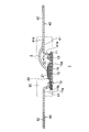
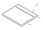
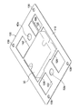
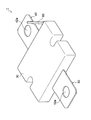
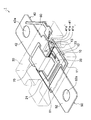
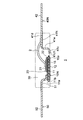
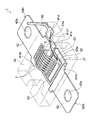
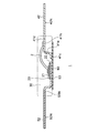
- FIG. 1 is a transparent perspective view of a semiconductor device according to a first embodiment. 1 is a cross-sectional view of a semiconductor device according to a first embodiment.
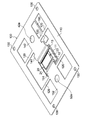
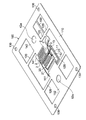
- FIG. 7 is a perspective view for illustrating the method for manufacturing the semiconductor device according to the first embodiment. It is a perspective view for demonstrating the manufacturing method of the semiconductor device which concerns on 1st Embodiment following FIG. 3A. It is a perspective view for demonstrating the manufacturing method of the semiconductor device which concerns on 1st Embodiment following FIG. 3B. It is a perspective view for demonstrating the manufacturing method of the semiconductor device which concerns on 1st Embodiment following FIG. 3C. It is a perspective view for demonstrating the manufacturing method of the semiconductor device which concerns on 1st Embodiment following FIG.
- 3D It is a perspective view for demonstrating the manufacturing method of the semiconductor device which concerns on 1st Embodiment following FIG. 3E. It is a see-through perspective view of the semiconductor device concerning a 2nd embodiment. It is a see-through perspective view of the semiconductor device concerning a 3rd embodiment. It is sectional drawing of the semiconductor device concerning 4th Embodiment. It is a see-through perspective view of the semiconductor device concerning a 5th embodiment. It is sectional drawing of the semiconductor device concerning 5th Embodiment.
- the semiconductor device 1 is a semiconductor device attached to a heat sink (not shown) such as a heat sink or a vehicle body.
- the semiconductor device 1 is a blinker relay, but the semiconductor device according to the present invention is not limited to this.
- the semiconductor device 1 includes an insulating substrate 10, a heat generating electronic component 20, a sealing portion 30, a lead member 40 (first lead member), and a lead member 50 (second lead member). ), A lead member 60 and a metal wire 2.
- the semiconductor device 1 is configured as, for example, a blinker relay. When the semiconductor device 1 is a blinker relay, one of the lead members 40 and 50 is electrically connected to a battery (not shown), and the other lead member is connected to a blinker switch (not shown). Electrically connected.
- the insulating substrate 10 is, as shown in FIG. 2, an insulating thermally conductive base material having a main surface 11a (first main surface) and a main surface 11b opposite to the first main surface (second main surface). 11, a component mounting land 12 formed on the main surface 11a, an isolated land 13 formed on the main surface 11a, and an exposed conductive portion 15 formed on the main surface 11b.
- the isolated land portion 13 is an isolated land and is electrically separated from the component mounting land portion 12.
- the exposed conductive portion 15 includes an exposed surface 15 a exposed from the sealing portion 30 and in contact with the heat dissipating member.
- the insulating substrate 10 is a ceramic substrate, but may be another insulating substrate.
- the component mounting lands 12, the isolated lands 13, and the exposed conductive portions 15 are made of a conductive material (copper in the present embodiment).
- the heat generating electronic component 20 is a device having a vertical structure, and as shown in FIGS. 1 and 2, the main electrode 21 (first main electrode) and the gate electrode 23 are provided on the upper surface, and the main electrode 22 (on the lower surface A second main electrode is provided.
- the main electrode 21 is a drain electrode
- the main electrode 22 is a source electrode.
- the heat generated by the heat generating electronic component 20 is dissipated to the heat dissipator through the component mounting land portion 12, the insulating heat conductive base 11 and the exposed conductive portion 15. Some heat is dissipated into the air through the seal 30.
- the heat generating electronic component 20 is a semiconductor switching element.
- the semiconductor switching element is, for example, a field effect transistor (Metal-Oxide-Semiconductor Field Effect Transistor: MOS FET), an Insulated Gate Bipolar Transistor (IGBT), or a thyristor.
- MOS FET Metal-Oxide-Semiconductor Field Effect Transistor
- IGBT Insulated Gate Bipolar Transistor
- the heat generating electronic component 20 may be another electronic component such as a diode.
- the heat generating electronic component 20 may be a device having a horizontal structure in which the main electrodes 21 and 22 and the gate electrode 23 are provided on the upper surface.
- the main electrode 22 and the component mounting land portion 12 are electrically connected by a metal wire, a connector or the like.
- the sealing portion 30 is made of, for example, an insulating resin material, and seals the insulating substrate 10, the heat-generating electronic component 20, the inner lead portions 41 and 51, and the metal wires 2 and 3.
- the back surface (exposed conductive portion 15) of the insulating substrate 10 is not sealed by the sealing portion 30.
- the lead member 40 has an inner lead portion 41 (first inner lead portion) sealed in the sealing portion 30, and an outer lead portion 42 (first outer lead portion) exposed from the sealing portion 30.
- the inner lead portion 41 has a heat radiation end 41 c, a vertically extending portion 41 e, and an electrical connection portion 41 d.
- the heat radiation end portion 41 c is provided at the tip of the inner lead portion 41 and configured to release the heat transmitted from the outer lead portion 42 to the heat radiating body.
- the electrical connection portion 41 d is located between the heat radiation end portion 41 c and the outer lead portion 42 and is electrically connected to the main electrode 21 of the heat-generating electronic component 20.
- the electrical connection portion 41 d is a portion sandwiched between the vertically extending portion 41 e and the outer lead portion 42.
- the vertically extending portion 41 e is provided to secure a predetermined insulation distance between the outer lead portion 42 and the heat radiating body.
- the heat radiation end 41 c of the inner lead portion 41 is electrically connected to the isolated land portion 13. Further, as shown in FIGS. 1 and 2, the main electrode 21 and the electrical connection portion 41 d of the inner lead portion 41 are electrically connected by the metal wire 2 (for example, Al wire) without interposing the isolated land portion 13. It is done. In the present embodiment, since a large current flows in the heat generating electronic component 20, a plurality of metal wires 2 are used. One end of the metal wire 2 is electrically connected to the top surface of the electrical connection portion 41 d of the inner lead portion 41 as shown in FIG.
- the metal wire 2 for example, Al wire
- the outer lead portion 42 is provided with a fixing hole 42 a used when fixing the semiconductor device 1 to the heat sink.
- the lead member 50 is electrically connected to the main electrode 22, and the inner lead portion 51 (second inner lead portion) sealed in the sealing portion 30, and the outer lead portion 52 exposed from the sealing portion 30 (second internal lead portion). A second outer lead portion).
- the inner lead portion 51 is electrically connected to the component mounting land portion 12.
- the outer lead portion 52 is provided with a fixing hole 52a used when fixing the semiconductor device 1 to the heat sink.
- the lead member 60 is electrically connected to the gate electrode 23 of the heat generating electronic component 20 via the metal wire 3 (for example, an Au wire).
- the lead member 60 is connected to a drive device (not shown) that outputs a control signal of the heat-generating electronic component 20.
- the main electrode 21 of the heat-generating electronic component 20 and the electrical connection portion 41 d of the inner lead portion 41 are electrically connected by the metal wire 2. That is, the main electrode 21 and the inner lead portion 41 are electrically connected without interposing the isolated land portion 13.
- the area of the isolated land portion 13 can be reduced as compared to the case where the metal wire 2 is connected to the isolated land portion 13.
- the cost of the insulating substrate 10 can be reduced.
- the heat dissipation end 41 c of the inner lead portion 41 is connected to the isolated land portion 13, and the heat transmitted from the outer lead portion 42 is dissipated to the heat dissipation body. That is, the heat generated in the external device and propagated into the semiconductor device 1 through the outer lead portion 42 is the heat radiation end portion 41 c of the inner lead portion 41, the isolated land portion 13, the insulating heat conductive base 11 and the exposed conductive portion 15. The heat is dissipated to the radiator through the Thus, the heat transmitted from the external device to the inside of the semiconductor device 1 can be efficiently dissipated to the heat sink. Therefore, according to the first embodiment, the cost of the semiconductor device 1 can be reduced while the cost is reduced. The heat transmitted from the device to the inside of the semiconductor device 1 can be efficiently dissipated to the heat sink.
- the insulating substrate 10 is prepared. As described above, the component mounting land 12 and the isolated land 13 are provided on the upper surface of the insulating heat conductive base 11. After preparation, claim solder (not shown) is applied to predetermined parts of the component mounting lands 12 and the isolated lands 13.
- the heat-generating electronic component 20 is mounted on the component mounting land portion 12 of the insulating substrate 10. More specifically, the heat generating electronic component 20 is mounted on the component mounting land 12 so that the main electrode 22 provided on the lower surface of the heat generating electronic component 20 is electrically connected to the component mounting land 12 via cream solder. Do.
- the lead frame 100 includes a frame portion 110, a plurality of tie bars 120, positioning holes 130 provided at four corners of the frame portion 110, lead frame terminal portions 141, 142, 151 and 152, and a lead frame gate terminal portion 160. And.
- the lead frame terminal portions 141 and 151 are portions to be the inner lead portions 41 and 51, respectively, and the lead frame terminal portions 142 and 152 are portions to be the outer lead portions 42 and 52, respectively.
- the lead frame gate terminal portion 160 is a portion to be the lead member 60.
- the lead frame terminal portions 151, 152 are provided with fixing holes 42a, 52a used when fixing the semiconductor device 1 to the heat sink.
- the lead frame 100 is placed on the insulating substrate 10. More specifically, alignment is performed such that the tip end portion of the lead frame terminal portion 141 is located on the isolated land portion 13 and the tip end portion of the lead frame terminal portion 151 is located on the component mounting land portion 12. Thereafter, through the reflow process, the heat-generating electronic component 20 is fixed to the insulating substrate 10, and the lead frame 100 is fixed to the insulating substrate 10.
- the main electrode 21 of the heat-generating electronic component 20 and the lead frame terminal portion 141 are electrically connected by a plurality of metal wires 2. Further, the gate electrode 23 of the heat-generating electronic component 20 and the lead frame gate terminal portion 160 are electrically connected by the metal wire 3.
- the metal wire 2 is an Al wire
- the metal wire 3 is an Au wire. The metal wires 2 and 3 are bonded to an object by ultrasonic vibration.
- the insulating substrate 10 the heat-generating electronic component 20, the lead frame terminal portions 141 and 151, and the metal wires 2 and 3 are sealed by transfer molding to form a sealing portion 30. .
- the back surface of the insulating substrate 10 is not sealed with resin, and the exposed conductive portion 15 is exposed.
- the frame 110 and the tie bar 120 are cut off to obtain the semiconductor device 1.
- Second Embodiment A semiconductor device 1 according to a second embodiment will be described with reference to FIG.
- a connector 70 is used in place of the metal wire 2.
- the second embodiment will be described focusing on differences from the first embodiment.
- the semiconductor device 1 includes the insulating substrate 10, the heat-generating electronic component 20, the sealing portion 30, the lead member 40, the lead member 50, and the lead member 60. , And a connector 70.
- the semiconductor device 1 includes the insulating substrate 10, the heat-generating electronic component 20, the sealing portion 30, the lead member 40, the lead member 50, and the lead member 60.
- a connector 70 is about components other than connector 70, since it is the same as that of a 1st embodiment, detailed explanation is omitted.
- the connector 70 is a conductive plate, and electrically connects the main electrode 21 of the heat-generating electronic component 20 and the electrical connection portion 41 d of the inner lead portion 41. More specifically, one end of the connector 70 is connected to the main electrode 21 via a solder, and the other end of the connector 70 is connected to the electrical connection portion 41 d of the inner lead portion 41 via a solder.
- the main electrode 21 of the heat-generating electronic component 20 and the electrical connection portion 41 d of the inner lead portion 41 are electrically connected by the connector 70. That is, the main electrode 21 and the inner lead portion 41 are electrically connected without interposing the isolated land portion 13. Further, the heat radiation end 41 c of the inner lead portion 41 is connected to the isolated land portion 13.
- the heat transmitted from the external device to the inside of the semiconductor device 1 is efficiently applied to the heat sink. Can dissipate heat.
- the connector 70 is used in place of the plurality of metal wires 2, the wire bonding step of the metal wires 2 is not necessary.
- the connector 70 is mounted on the main electrode 21 and the inner lead portion 41 via cream solder. Place and secure in the subsequent reflow process.
- the manufacturing process of the semiconductor device can be simplified, and thus the cost of the semiconductor device 1 can be further reduced.
- a semiconductor device 1 according to a third embodiment will be described with reference to FIG.
- the third embodiment not the metal wire 2 but the lead member 40 is directly connected to the main electrode 21.
- the third embodiment will be described below focusing on the differences from the first embodiment.
- the semiconductor device 1 includes the insulating substrate 10, the heat-generating electronic component 20, the sealing portion 30, the lead member 40 M, the lead member 50, and the lead member 60. And. About components other than lead member 40M, since it is the same as that of a 1st embodiment, detailed explanation is omitted.
- the lead member 40M has an inner lead portion 41M sealed in the sealing portion 30, and an outer lead portion 42 exposed from the sealing portion 30.
- the inner lead portion 41M further includes an extended connection portion 41a in addition to the heat dissipation end portion 41c and the electrical connection portion 41d.
- the extended connection portion 41 a extends from the electrical connection portion 41 d and is electrically connected to the main electrode 21 of the heat-generating electronic component 20.
- the inner lead portion 41 ⁇ / b> M is bent so that both end portions of the inner lead portion 41 ⁇ / b> M contact the isolated land portion 13.
- the shape of the inner lead portion 41M is not limited to this.
- the extended connection portion 41a of the inner lead portion 41M is electrically connected to the main electrode 21 of the heat generating electronic component 20 and the heat transmitted from the outer lead portion 42 Is dissipated to the heat dissipation body through the heat dissipation end 41 c of the inner lead portion 41. That is, the heat generated in the external device and propagated into the semiconductor device 1 through the outer lead portion 42 is dissipated to the heat dissipation body through the heat dissipation end 41 c, the isolated land portion 13, the insulating heat conductive base 11 and the exposed conductive portion 15 Be done.
- the heat transmitted from the external device to the inside of the semiconductor device 1 can be efficiently applied to the heat sink while reducing the cost of the semiconductor device 1. Can dissipate heat.
- the inner lead portion 41M is configured to be connected to both the main electrode 21 and the isolated land portion 13 without using the metal wire 2 and the connector 70.
- the manufacturing process can be simplified. Therefore, according to the third embodiment, the cost of the semiconductor device 1 can be further reduced.
- a semiconductor device 1 according to the fourth embodiment will be described with reference to FIG.
- the inner lead portion is directly connected to the heat dissipating member without interposing the insulating substrate.
- the fourth embodiment will be described below focusing on the differences with the first embodiment.
- the semiconductor device 1 includes the insulating substrate 10N, the heat-generating electronic component 20, the sealing portion 30, the lead member 40N, the lead member 50, and the lead member 60. And. Components other than the insulating substrate 10 ⁇ / b> N and the lead member 40 ⁇ / b> M are the same as those in the first embodiment, and thus detailed description will be omitted.
- the insulating substrate 10N has an insulating thermally conductive base 11 having a major surface 11a and a major surface 11b, and a component mounting land 12 formed on the major surface 11a. Since the isolated land portion 13 is not provided, the area of the insulating substrate 10N is smaller than that of the insulating substrate 10 of the first to third embodiments.
- the lead member 40N has an inner lead portion 41N sealed in the sealing portion 30, and an outer lead portion 42 exposed from the sealing portion 30.
- the heat release end 41c of the inner lead portion 41N includes an exposed surface (lower surface in FIG. 6) 41c1.
- the exposed surface 41c1 is exposed from the sealing portion 30, and is in contact with the heat sink in a state where the semiconductor device 1 is attached to the heat sink.
- the main electrode 21 and the inner lead portion 41N are electrically connected by the metal wire 2 as shown in FIG. That is, one end of the metal wire 2 is electrically connected to the main electrode 21 of the heat generating electronic component 20, and the other end of the metal wire 2 is electrically connected to the inner lead portion 41N. More specifically, the other end of the metal wire 2 is electrically connected to an electrical connection portion 41d of the inner lead portion 41N sandwiched between the vertically extending portion 41e and the outer lead portion 42.
- the inner lead portion 41N is electrically connected to the main electrode 21 of the heat generating electronic component 20 without passing through the land portion on the insulating heat conductive substrate 11.
- the heat transmitted from the outer lead portion 42 is configured to be dissipated through the heat dissipation end 41 c directly connected to the heat dissipation body. That is, the heat generated in the external device and propagated into the semiconductor device 1 through the outer lead portion 42 is dissipated to the heat sink through the heat dissipation end 41 c of the inner lead portion 41 N without passing through the insulating substrate 10 N.
- the heat transmitted into the semiconductor device 1 can be dissipated more efficiently to the heat sink because the insulating substrate is not interposed.
- the heat transmitted from the external device to the inside of the semiconductor device 1 can be efficiently dissipated to the heat dissipation body while achieving cost reduction of the semiconductor device 1.
- the area of the insulating substrate can be reduced by the amount of absence of the isolated lands, so the cost of the insulating substrate can be reduced. Therefore, according to the fourth embodiment, the cost of the semiconductor device 1 can be further reduced.
- the main electrode 21 and the inner lead portion 41N are connected by the metal wire 2.
- the present invention is not limited to this, and may be connected by a connector as in the second embodiment.
- the inner lead portion 41N may be directly connected to the main electrode 21.
- a semiconductor device 1 according to the fifth embodiment will be described with reference to FIG. 7 and FIG.
- the heat-generating electronic component is mounted on the inner lead portion without using the insulating substrate.
- the fifth embodiment will be described focusing on differences from the first embodiment.
- the semiconductor device 1 includes the heat generating electronic component 20, the sealing portion 30, the lead member 40N, the lead member 50N, the lead member 60, and the insulation. And a seat 80.
- the heat-generating electronic component 20, the sealing portion 30, and the lead member 60 are the same as in the first embodiment, and the lead member 40N is the same as in the fourth embodiment. Do.
- the lead member 50N has an inner lead portion 51N sealed in the sealing portion 30, and an outer lead portion 52 exposed from the sealing portion 30.
- the inner lead portion 51N has a component mounting portion (die pad) 53, as shown in FIG. 7 and FIG.
- the component mounting portion 53 includes an exposed surface 53 a exposed from the sealing portion 30.
- the exposed surface 53a is in contact with the heat sink in a state where the semiconductor device 1 is attached to the heat sink.
- the heat-generating electronic component 20 is mounted on the component mounting portion 53. More specifically, the heat generating electronic component 20 is mounted on the component mounting portion 53 such that the main electrode 22 is electrically connected to the component mounting portion 53 via a solder.
- the heat-generating electronic component 20 is a device having a horizontal structure, the main electrode 22 and the component mounting portion 53 are electrically connected by a metal wire, a connector, or the like.
- the insulating sheet 80 is made of an insulating material (for example, polyimide, PET or the like), and is adhered to the sealing portion 30 so as to cover the exposed surface 41c1 of the heat radiation end 41c and the exposed surface 53a of the component mounting portion 53.
- the insulating sheet 80 prevents the occurrence of a short circuit between the heat radiation end 41 c and the component mounting portion 53 in the state where the semiconductor device 1 is attached to the conductive heat radiator.
- the insulating sheet 80 is not an essential component of the semiconductor device of the present embodiment, and the insulating sheet 80 may be provided on the heat sink side.
- the inner lead portion 41N is electrically connected to the main electrode 21 of the heat generating electronic component 20 without passing through the land portion on the insulating base and the outer lead portion 42.
- the heat transmitted from the heat source is dissipated to the heat radiating body through the heat radiating end 41c. That is, the heat generated in the external device and propagated into the semiconductor device 1 through the outer lead portion 42 is dissipated to the radiator through the heat radiation end 41 c.
- the heat transmitted into the semiconductor device 1 can be dissipated more efficiently to the heat sink because the insulating substrate is not interposed.
- the heat transmitted from the external device to the inside of the semiconductor device 1 can be efficiently dissipated to the heat dissipation body while achieving cost reduction of the semiconductor device 1.
- the insulating substrate 10 since the insulating substrate 10 is not used, the parts cost and the manufacturing cost of the semiconductor device 1 can be significantly reduced.
- the main electrode 21 and the inner lead portion 41N are connected by the metal wire 2.
- the present invention is not limited to this, and may be connected by a connector as in the second embodiment.
- the inner lead portion 41N may be directly connected to the main electrode 21.
- the component mounting part 53 is exposed from the sealing part 30 in this embodiment, this invention is not limited to this, The component mounting part 53 may be embed
Landscapes
- Cooling Or The Like Of Semiconductors Or Solid State Devices (AREA)
- Engineering & Computer Science (AREA)
- Microelectronics & Electronic Packaging (AREA)
Abstract
Description
放熱体に取り付けられる半導体装置であって、
第1の主電極および第2の主電極を有する発熱電子部品と、
前記発熱電子部品を封止する封止部と、
前記封止部に封止された第1のインナーリード部、および前記封止部から露出した第1のアウターリード部を有する第1のリード部材と、
前記第2の主電極に電気的に接続され、前記封止部に封止された第2のインナーリード部、および前記封止部から露出した第2のアウターリード部を有する第2のリード部材と、を備え、
前記第1のインナーリード部は、前記第1のアウターリード部から伝播する熱を前記放熱体に逃がす放熱端部と、前記放熱端部および前記第1のアウターリード部の間に位置し且つ前記発熱電子部品の前記第1の主電極に電気的に接続される電気接続部とを有することを特徴とする。
第1の主面および前記第1の主面と反対側の第2の主面を有する絶縁性熱伝導基材と、前記第1の主面に形成された部品実装ランド部と、を有する絶縁基板をさらに備え、
前記第2のリード部材の前記第2のインナーリード部は、前記部品実装ランド部に電気的に接続されていてもよい。
前記絶縁基板は、前記絶縁性熱伝導基材の前記第1の主面に形成され、前記部品実装ランド部から電気的に分離された孤立ランド部をさらに有し、
前記第1のインナーリード部の前記放熱端部は、前記孤立ランド部に電気的に接続され、
前記第1の主電極と前記第1のインナーリード部の前記電気接続部とは、金属ワイヤーにより、前記孤立ランド部を介さずに電気的に接続されていてもよい。
前記絶縁基板は、前記絶縁性熱伝導基材の前記第1の主面に形成され、前記部品実装ランド部から電気的に分離された孤立ランド部をさらに有し、
前記第1のインナーリード部の前記放熱端部は、前記孤立ランド部に電気的に接続され、
前記第1の主電極と前記第1のインナーリード部の前記電気接続部とは、接続子により、前記孤立ランド部を介さずに電気的に接続されていてもよい。
前記絶縁基板は、前記絶縁性熱伝導基材の前記第1の主面に形成され、前記部品実装ランド部から電気的に分離された孤立ランド部をさらに有し、
前記第1のインナーリード部の前記放熱端部は、前記孤立ランド部に電気的に接続され、
前記第1のインナーリード部は、前記電気接続部から延在し且つ前記発熱電子部品の前記第1の主電極に電気的に接続する延在接続部を有してもよい。
前記第1のインナーリード部の前記放熱端部は、前記封止部から露出した露出面を含んでもよい。
前記絶縁基板は、前記絶縁性熱伝導基材の前記第2の主面に形成された露出導電部をさらに有し、前記露出導電部は、前記封止部から露出し前記放熱体と接する露出面を含んでもよい。
前記第1のインナーリード部の前記放熱端部は、前記封止部から露出した露出面を含み、
前記第2のインナーリード部は部品実装部を有しており、前記発熱電子部品は、前記第2の主電極が前記部品実装部に電気的に接続されるように前記部品実装部の上に実装されているようにしてもよい。
前記部品実装部は、前記封止部から露出した露出面を含み、
前記第1のインナーリード部の前記放熱端部の露出面および前記部品実装部の露出面を被覆するように前記封止部に貼着された絶縁シートをさらに備えてもよい。
前記第1の主電極と前記第1のインナーリード部とは、金属ワイヤーにより電気的に接続されていてもよい。
前記第1の主電極と前記第1のインナーリード部とは、接続子により電気的に接続されていてもよい。
前記第1のインナーリード部は、前記電気接続部から延在し且つ前記発熱電子部品の前記第1の主電極に電気的に接続される延在接続部を有してもよい。
前記発熱電子部品は、ゲート電極をさらに有する半導体スイッチング素子であってもよい。
前記第1の主電極および前記ゲート電極は前記発熱電子部品の上面に設けられ、前記第2の主電極は前記発熱電子部品の下面に設けられていてもよい。
前記第1のリード部材および前記第2のリード部材のうち、一方のリード部材がバッテリーに電気的に接続され、他方のリード部材がウィンカースイッチに電気的に接続されてもよい。
第1の実施形態に係る半導体装置1について図1および図2を参照して説明する。
よって、第1の実施形態によれば、半導体装置1の低コスト化を図りつつ、外部装置から半導体装置1の内部に伝播する熱を放熱体に効率的に放熱することができる。
上記の半導体装置1の製造方法について、図3A~図3Fを参照して説明する。
第2の実施形態に係る半導体装置1について図4を参照して説明する。第2の実施形態では、金属ワイヤー2に代えて接続子70を用いる。以下、第1の実施形態との相違点を中心に第2の実施形態について説明する。
第3の実施形態に係る半導体装置1について図5を参照して説明する。第3の実施形態では、金属ワイヤー2ではなく、リード部材40が主電極21に直接接続される。以下、第1の実施形態との相違点を中心に第3の実施形態について説明する。
第4の実施形態に係る半導体装置1について図6を参照して説明する。第4の実施形態では、インナーリード部が絶縁基板を介さずに、放熱体に直接接続される。以下、第1の実施形態との相違点を中心に第4の実施形態について説明する。
第5の実施形態に係る半導体装置1について図7および図8を参照して説明する。第5の実施形態では、絶縁基板を用いず、発熱電子部品はインナーリード部の上に実装される。以下、第1の実施形態との相違点を中心に第5の実施形態について説明する。
2,3 金属ワイヤー
10,10N 絶縁基板
11 絶縁性熱伝導基材
11a,11b 主面
12 部品実装ランド部
13 孤立ランド部
15 露出導電部
20 発熱電子部品
21,22 主電極
23 ゲート電極
30 封止部
40,40M,40N,50,50N,60 リード部材
41,41M,41N,51,51N インナーリード部
41a 延在接続部
41c 放熱端部
41d 電気接続部
41e 垂直延在部
42,52 アウターリード部
42a,52a 固定用孔
41c1,53a 露出面
53 部品実装部
70 接続子
80 絶縁シート
100 リードフレーム
110 枠部
120 タイバー
130 位置決め孔
141,142,151,152 リードフレーム端子部
160 リードフレームゲート端子部
Claims (15)
- 放熱体に取り付けられる半導体装置であって、
第1の主電極および第2の主電極を有する発熱電子部品と、
前記発熱電子部品を封止する封止部と、
前記封止部に封止された第1のインナーリード部、および前記封止部から露出した第1のアウターリード部を有する第1のリード部材と、
前記第2の主電極に電気的に接続され、前記封止部に封止された第2のインナーリード部、および前記封止部から露出した第2のアウターリード部を有する第2のリード部材と、を備え、
前記第1のインナーリード部は、前記第1のアウターリード部から伝播する熱を前記放熱体に逃がす放熱端部と、前記放熱端部および前記第1のアウターリード部の間に位置し且つ前記発熱電子部品の前記第1の主電極に電気的に接続される電気接続部とを有することを特徴とする半導体装置。 - 第1の主面および前記第1の主面と反対側の第2の主面を有する絶縁性熱伝導基材と、前記第1の主面に形成された部品実装ランド部と、を有する絶縁基板をさらに備え、
前記第2のリード部材の前記第2のインナーリード部は、前記部品実装ランド部に電気的に接続されていることを特徴とする請求項1に記載の半導体装置。 - 前記絶縁基板は、前記絶縁性熱伝導基材の前記第1の主面に形成され、前記部品実装ランド部から電気的に分離された孤立ランド部をさらに有し、
前記第1のインナーリード部の前記放熱端部は、前記孤立ランド部に電気的に接続され、
前記第1の主電極と前記第1のインナーリード部の前記電気接続部とは、金属ワイヤーにより、前記孤立ランド部を介さずに電気的に接続されていることを特徴とする請求項2に記載の半導体装置。 - 前記絶縁基板は、前記絶縁性熱伝導基材の前記第1の主面に形成され、前記部品実装ランド部から電気的に分離された孤立ランド部をさらに有し、
前記第1のインナーリード部の前記放熱端部は、前記孤立ランド部に電気的に接続され、
前記第1の主電極と前記第1のインナーリード部の前記電気接続部とは、接続子により、前記孤立ランド部を介さずに電気的に接続されていることを特徴とする請求項2に記載の半導体装置。 - 前記絶縁基板は、前記絶縁性熱伝導基材の前記第1の主面に形成され、前記部品実装ランド部から電気的に分離された孤立ランド部をさらに有し、
前記第1のインナーリード部の前記放熱端部は、前記孤立ランド部に電気的に接続され、
前記第1のインナーリード部は、前記電気接続部から延在し且つ前記発熱電子部品の前記第1の主電極に電気的に接続する延在接続部を有することを特徴とする請求項2に記載の半導体装置。 - 前記第1のインナーリード部の前記放熱端部は、前記封止部から露出した露出面を含むことを特徴とする請求項2に記載の半導体装置。
- 前記絶縁基板は、前記絶縁性熱伝導基材の前記第2の主面に形成された露出導電部をさらに有し、前記露出導電部は、前記封止部から露出し前記放熱体と接する露出面を含むことを特徴とする請求項2に記載の半導体装置。
- 前記第1のインナーリード部の前記放熱端部は、前記封止部から露出した露出面を含み、
前記第2のインナーリード部は部品実装部を有しており、前記発熱電子部品は、前記第2の主電極が前記部品実装部に電気的に接続されるように前記部品実装部の上に実装されていることを特徴とする請求項1に記載の半導体装置。 - 前記部品実装部は、前記封止部から露出した露出面を含み、
前記第1のインナーリード部の前記放熱端部の露出面および前記部品実装部の露出面を被覆するように前記封止部に貼着された絶縁シートをさらに備えることを特徴とする請求項8に記載の半導体装置。 - 前記第1の主電極と前記第1のインナーリード部とは、金属ワイヤーにより電気的に接続されていることを特徴とする請求項8に記載の半導体装置。
- 前記第1の主電極と前記第1のインナーリード部とは、接続子により電気的に接続されていることを特徴とする請求項8に記載の半導体装置。
- 前記第1のインナーリード部は、前記電気接続部から延在し且つ前記発熱電子部品の前記第1の主電極に電気的に接続される延在接続部を有することを特徴とする請求項8に記載の半導体装置。
- 前記発熱電子部品は、ゲート電極をさらに有する半導体スイッチング素子であることを特徴とする請求項1に記載の半導体装置。
- 前記第1の主電極および前記ゲート電極は前記発熱電子部品の上面に設けられ、前記第2の主電極は前記発熱電子部品の下面に設けられていることを特徴とする請求項13に記載の半導体装置。
- 前記第1のリード部材および前記第2のリード部材のうち、一方のリード部材がバッテリーに電気的に接続され、他方のリード部材がウィンカースイッチに電気的に接続されることを特徴とする請求項13に記載の半導体装置。
Priority Applications (5)
| Application Number | Priority Date | Filing Date | Title |
|---|---|---|---|
| CN201780016796.1A CN110959191B (zh) | 2017-08-24 | 2017-08-24 | 半导体装置 |
| US16/085,921 US11315850B2 (en) | 2017-08-24 | 2017-08-24 | Semiconductor device |
| JP2018535446A JP6602981B2 (ja) | 2017-08-24 | 2017-08-24 | 半導体装置 |
| PCT/JP2017/030280 WO2019038876A1 (ja) | 2017-08-24 | 2017-08-24 | 半導体装置 |
| GB1815305.6A GB2567746B (en) | 2017-08-24 | 2017-08-24 | Semiconductor device |
Applications Claiming Priority (1)
| Application Number | Priority Date | Filing Date | Title |
|---|---|---|---|
| PCT/JP2017/030280 WO2019038876A1 (ja) | 2017-08-24 | 2017-08-24 | 半導体装置 |
Publications (1)
| Publication Number | Publication Date |
|---|---|
| WO2019038876A1 true WO2019038876A1 (ja) | 2019-02-28 |
Family
ID=64024314
Family Applications (1)
| Application Number | Title | Priority Date | Filing Date |
|---|---|---|---|
| PCT/JP2017/030280 Ceased WO2019038876A1 (ja) | 2017-08-24 | 2017-08-24 | 半導体装置 |
Country Status (5)
| Country | Link |
|---|---|
| US (1) | US11315850B2 (ja) |
| JP (1) | JP6602981B2 (ja) |
| CN (1) | CN110959191B (ja) |
| GB (1) | GB2567746B (ja) |
| WO (1) | WO2019038876A1 (ja) |
Families Citing this family (5)
| Publication number | Priority date | Publication date | Assignee | Title |
|---|---|---|---|---|
| JP6740959B2 (ja) * | 2017-05-17 | 2020-08-19 | 株式会社オートネットワーク技術研究所 | 回路装置 |
| WO2020194480A1 (ja) * | 2019-03-25 | 2020-10-01 | 新電元工業株式会社 | 半導体装置、リードフレーム及び電源装置 |
| US11270969B2 (en) * | 2019-06-04 | 2022-03-08 | Jmj Korea Co., Ltd. | Semiconductor package |
| DE102022103310B4 (de) * | 2022-02-11 | 2024-07-11 | Semikron Danfoss GmbH | Leistungsformmodul und Leistungsmodul-Baugruppe |
| US20240222255A1 (en) * | 2022-12-30 | 2024-07-04 | Power Master Semiconductor Co., Ltd. | Semiconductor device |
Citations (5)
| Publication number | Priority date | Publication date | Assignee | Title |
|---|---|---|---|---|
| JP2006294729A (ja) * | 2005-04-07 | 2006-10-26 | Toshiba Corp | 半導体装置 |
| US20100277873A1 (en) * | 2009-03-28 | 2010-11-04 | Danfoss Silicon Power Gmbh | Method for manufacturing a rigid power module suited for high-voltage applications |
| JP2011243752A (ja) * | 2010-05-18 | 2011-12-01 | Panasonic Corp | 半導体装置の製造方法、半導体内部接続部材および半導体内部接続部材群 |
| US20150179556A1 (en) * | 2013-12-20 | 2015-06-25 | Samsung Electro-Mechanics Co., Ltd. | Semiconductor package and method of manufacturing the same |
| US20150179552A1 (en) * | 2013-12-24 | 2015-06-25 | Samsung Electro-Mechanics Co., Ltd. | Semiconductor package and manufacturing method thereof |
Family Cites Families (17)
| Publication number | Priority date | Publication date | Assignee | Title |
|---|---|---|---|---|
| JPH08222673A (ja) * | 1995-02-14 | 1996-08-30 | Toppan Printing Co Ltd | リードフレーム |
| JPH10242368A (ja) * | 1997-02-25 | 1998-09-11 | Hitachi Ltd | 半導体装置およびその製造方法ならびに半導体モジュールおよびicカード |
| KR100723454B1 (ko) * | 2004-08-21 | 2007-05-30 | 페어차일드코리아반도체 주식회사 | 높은 열 방출 능력을 구비한 전력용 모듈 패키지 및 그제조방법 |
| JP4248528B2 (ja) * | 2002-10-24 | 2009-04-02 | パナソニック株式会社 | リードフレーム及び該リードフレームを用いる樹脂封止型半導体装置の製造方法 |
| JP4319591B2 (ja) | 2004-07-15 | 2009-08-26 | 株式会社日立製作所 | 半導体パワーモジュール |
| JPWO2007026944A1 (ja) * | 2005-08-31 | 2009-03-12 | 三洋電機株式会社 | 回路装置およびその製造方法 |
| JP5332374B2 (ja) * | 2008-07-25 | 2013-11-06 | サンケン電気株式会社 | 半導体装置 |
| US8097944B2 (en) * | 2009-04-30 | 2012-01-17 | Infineon Technologies Ag | Semiconductor device |
| EP2581937B1 (en) * | 2010-06-11 | 2017-09-06 | Panasonic Intellectual Property Management Co., Ltd. | Resin-sealed semiconductor device and method for manufacturing same |
| JP5819052B2 (ja) * | 2010-09-09 | 2015-11-18 | ローム株式会社 | 半導体装置および半導体装置の製造方法 |
| US9147637B2 (en) * | 2011-12-23 | 2015-09-29 | Infineon Technologies Ag | Module including a discrete device mounted on a DCB substrate |
| JP2013258354A (ja) * | 2012-06-14 | 2013-12-26 | Denso Corp | モールドパッケージおよびその製造方法 |
| US9859250B2 (en) * | 2013-12-20 | 2018-01-02 | Cyntec Co., Ltd. | Substrate and the method to fabricate thereof |
| JP6305302B2 (ja) | 2014-10-02 | 2018-04-04 | 三菱電機株式会社 | 半導体装置およびその製造方法 |
| US9704828B2 (en) * | 2014-10-16 | 2017-07-11 | Shindengen Electric Manufacturing Co., Ltd. | Semiconductor module |
| JPWO2016162991A1 (ja) * | 2015-04-08 | 2017-08-24 | 三菱電機株式会社 | 半導体装置および半導体装置の製造方法 |
| US9997437B2 (en) * | 2015-04-28 | 2018-06-12 | Shindengen Electric Manufacturing Co., Ltd. | Power semiconductor module for improved thermal performance |
-
2017
- 2017-08-24 GB GB1815305.6A patent/GB2567746B/en active Active
- 2017-08-24 JP JP2018535446A patent/JP6602981B2/ja active Active
- 2017-08-24 WO PCT/JP2017/030280 patent/WO2019038876A1/ja not_active Ceased
- 2017-08-24 CN CN201780016796.1A patent/CN110959191B/zh active Active
- 2017-08-24 US US16/085,921 patent/US11315850B2/en active Active
Patent Citations (5)
| Publication number | Priority date | Publication date | Assignee | Title |
|---|---|---|---|---|
| JP2006294729A (ja) * | 2005-04-07 | 2006-10-26 | Toshiba Corp | 半導体装置 |
| US20100277873A1 (en) * | 2009-03-28 | 2010-11-04 | Danfoss Silicon Power Gmbh | Method for manufacturing a rigid power module suited for high-voltage applications |
| JP2011243752A (ja) * | 2010-05-18 | 2011-12-01 | Panasonic Corp | 半導体装置の製造方法、半導体内部接続部材および半導体内部接続部材群 |
| US20150179556A1 (en) * | 2013-12-20 | 2015-06-25 | Samsung Electro-Mechanics Co., Ltd. | Semiconductor package and method of manufacturing the same |
| US20150179552A1 (en) * | 2013-12-24 | 2015-06-25 | Samsung Electro-Mechanics Co., Ltd. | Semiconductor package and manufacturing method thereof |
Also Published As
| Publication number | Publication date |
|---|---|
| US20200381327A1 (en) | 2020-12-03 |
| JP6602981B2 (ja) | 2019-11-06 |
| US11315850B2 (en) | 2022-04-26 |
| CN110959191B (zh) | 2023-10-20 |
| JPWO2019038876A1 (ja) | 2019-11-07 |
| GB201815305D0 (en) | 2018-11-07 |
| GB2567746B (en) | 2022-03-16 |
| CN110959191A (zh) | 2020-04-03 |
| GB2567746A (en) | 2019-04-24 |
Similar Documents
| Publication | Publication Date | Title |
|---|---|---|
| JP5257817B2 (ja) | 半導体装置 | |
| CN102315181B (zh) | 半导体器件 | |
| US9171773B2 (en) | Semiconductor device | |
| KR101173927B1 (ko) | 반도체장치 모듈 | |
| WO2019038876A1 (ja) | 半導体装置 | |
| JP2015076562A (ja) | パワーモジュール | |
| CN104916614A (zh) | 半导体装置及其制造方法 | |
| JP3599057B2 (ja) | 半導体装置 | |
| JP4899481B2 (ja) | 外部に露出する放熱体を上部に有する樹脂封止型半導体装置の製法 | |
| JP2017123360A (ja) | 半導体モジュール | |
| CN107301987A (zh) | 半导体装置的散热结构 | |
| JP2008042041A (ja) | 半導体装置 | |
| JP2004221381A (ja) | 半導体装置 | |
| JP2013183022A (ja) | 半導体装置および半導体装置の製造方法 | |
| JP2009231685A (ja) | パワー半導体装置 | |
| JP2017005129A (ja) | 半導体装置 | |
| JP2020053623A (ja) | パワーユニット、パワーユニットの製造方法及びパワーユニットを有する電気装置 | |
| JP4797492B2 (ja) | 半導体装置 | |
| JP7050487B2 (ja) | 電子デバイス | |
| JP4861200B2 (ja) | パワーモジュール | |
| JP4649948B2 (ja) | 半導体装置 | |
| JP6771581B2 (ja) | 半導体モジュール及び半導体装置 | |
| CN115668488A (zh) | 半导体模块的安装结构 | |
| JP2020072102A (ja) | パワーユニット、パワーユニットの製造方法及びパワーユニットを有する電気装置 | |
| JP2011066281A (ja) | 発熱デバイス |
Legal Events
| Date | Code | Title | Description |
|---|---|---|---|
| ENP | Entry into the national phase |
Ref document number: 2018535446 Country of ref document: JP Kind code of ref document: A |
|
| WWE | Wipo information: entry into national phase |
Ref document number: 1815305.6 Country of ref document: GB |
|
| ENP | Entry into the national phase |
Ref document number: 201815305 Country of ref document: GB Kind code of ref document: A Free format text: PCT FILING DATE = 20170824 |
|
| 121 | Ep: the epo has been informed by wipo that ep was designated in this application |
Ref document number: 17922606 Country of ref document: EP Kind code of ref document: A1 |
|
| NENP | Non-entry into the national phase |
Ref country code: DE |
|
| 122 | Ep: pct application non-entry in european phase |
Ref document number: 17922606 Country of ref document: EP Kind code of ref document: A1 |