US11270969B2 - Semiconductor package - Google Patents
Semiconductor package Download PDFInfo
- Publication number
- US11270969B2 US11270969B2 US16/847,696 US202016847696A US11270969B2 US 11270969 B2 US11270969 B2 US 11270969B2 US 202016847696 A US202016847696 A US 202016847696A US 11270969 B2 US11270969 B2 US 11270969B2
- Authority
- US
- United States
- Prior art keywords
- chip
- lead
- pad
- edge
- semiconductor package
- Prior art date
- Legal status (The legal status is an assumption and is not a legal conclusion. Google has not performed a legal analysis and makes no representation as to the accuracy of the status listed.)
- Active, expires
Links
Images


Classifications
-
- H—ELECTRICITY
- H01—ELECTRIC ELEMENTS
- H01L—SEMICONDUCTOR DEVICES NOT COVERED BY CLASS H10
- H01L24/00—Arrangements for connecting or disconnecting semiconductor or solid-state bodies; Methods or apparatus related thereto
- H01L24/01—Means for bonding being attached to, or being formed on, the surface to be connected, e.g. chip-to-package, die-attach, "first-level" interconnects; Manufacturing methods related thereto
- H01L24/34—Strap connectors, e.g. copper straps for grounding power devices; Manufacturing methods related thereto
- H01L24/39—Structure, shape, material or disposition of the strap connectors after the connecting process
- H01L24/41—Structure, shape, material or disposition of the strap connectors after the connecting process of a plurality of strap connectors
-
- H—ELECTRICITY
- H01—ELECTRIC ELEMENTS
- H01L—SEMICONDUCTOR DEVICES NOT COVERED BY CLASS H10
- H01L23/00—Details of semiconductor or other solid state devices
- H01L23/02—Containers; Seals
- H01L23/04—Containers; Seals characterised by the shape of the container or parts, e.g. caps, walls
- H01L23/043—Containers; Seals characterised by the shape of the container or parts, e.g. caps, walls the container being a hollow construction and having a conductive base as a mounting as well as a lead for the semiconductor body
- H01L23/047—Containers; Seals characterised by the shape of the container or parts, e.g. caps, walls the container being a hollow construction and having a conductive base as a mounting as well as a lead for the semiconductor body the other leads being parallel to the base
-
- H—ELECTRICITY
- H01—ELECTRIC ELEMENTS
- H01L—SEMICONDUCTOR DEVICES NOT COVERED BY CLASS H10
- H01L23/00—Details of semiconductor or other solid state devices
- H01L23/28—Encapsulations, e.g. encapsulating layers, coatings, e.g. for protection
- H01L23/31—Encapsulations, e.g. encapsulating layers, coatings, e.g. for protection characterised by the arrangement or shape
- H01L23/3107—Encapsulations, e.g. encapsulating layers, coatings, e.g. for protection characterised by the arrangement or shape the device being completely enclosed
- H01L23/3114—Encapsulations, e.g. encapsulating layers, coatings, e.g. for protection characterised by the arrangement or shape the device being completely enclosed the device being a chip scale package, e.g. CSP
-
- H—ELECTRICITY
- H01—ELECTRIC ELEMENTS
- H01L—SEMICONDUCTOR DEVICES NOT COVERED BY CLASS H10
- H01L23/00—Details of semiconductor or other solid state devices
- H01L23/28—Encapsulations, e.g. encapsulating layers, coatings, e.g. for protection
- H01L23/31—Encapsulations, e.g. encapsulating layers, coatings, e.g. for protection characterised by the arrangement or shape
- H01L23/3107—Encapsulations, e.g. encapsulating layers, coatings, e.g. for protection characterised by the arrangement or shape the device being completely enclosed
- H01L23/3142—Sealing arrangements between parts, e.g. adhesion promotors
-
- H—ELECTRICITY
- H01—ELECTRIC ELEMENTS
- H01L—SEMICONDUCTOR DEVICES NOT COVERED BY CLASS H10
- H01L23/00—Details of semiconductor or other solid state devices
- H01L23/48—Arrangements for conducting electric current to or from the solid state body in operation, e.g. leads, terminal arrangements ; Selection of materials therefor
- H01L23/488—Arrangements for conducting electric current to or from the solid state body in operation, e.g. leads, terminal arrangements ; Selection of materials therefor consisting of soldered or bonded constructions
- H01L23/495—Lead-frames or other flat leads
- H01L23/49503—Lead-frames or other flat leads characterised by the die pad
- H01L23/49513—Lead-frames or other flat leads characterised by the die pad having bonding material between chip and die pad
-
- H—ELECTRICITY
- H01—ELECTRIC ELEMENTS
- H01L—SEMICONDUCTOR DEVICES NOT COVERED BY CLASS H10
- H01L23/00—Details of semiconductor or other solid state devices
- H01L23/48—Arrangements for conducting electric current to or from the solid state body in operation, e.g. leads, terminal arrangements ; Selection of materials therefor
- H01L23/488—Arrangements for conducting electric current to or from the solid state body in operation, e.g. leads, terminal arrangements ; Selection of materials therefor consisting of soldered or bonded constructions
- H01L23/495—Lead-frames or other flat leads
- H01L23/49517—Additional leads
- H01L23/49524—Additional leads the additional leads being a tape carrier or flat leads
-
- H—ELECTRICITY
- H01—ELECTRIC ELEMENTS
- H01L—SEMICONDUCTOR DEVICES NOT COVERED BY CLASS H10
- H01L23/00—Details of semiconductor or other solid state devices
- H01L23/48—Arrangements for conducting electric current to or from the solid state body in operation, e.g. leads, terminal arrangements ; Selection of materials therefor
- H01L23/488—Arrangements for conducting electric current to or from the solid state body in operation, e.g. leads, terminal arrangements ; Selection of materials therefor consisting of soldered or bonded constructions
- H01L23/495—Lead-frames or other flat leads
- H01L23/49541—Geometry of the lead-frame
- H01L23/49548—Cross section geometry
- H01L23/49551—Cross section geometry characterised by bent parts
-
- H—ELECTRICITY
- H01—ELECTRIC ELEMENTS
- H01L—SEMICONDUCTOR DEVICES NOT COVERED BY CLASS H10
- H01L23/00—Details of semiconductor or other solid state devices
- H01L23/48—Arrangements for conducting electric current to or from the solid state body in operation, e.g. leads, terminal arrangements ; Selection of materials therefor
- H01L23/488—Arrangements for conducting electric current to or from the solid state body in operation, e.g. leads, terminal arrangements ; Selection of materials therefor consisting of soldered or bonded constructions
- H01L23/495—Lead-frames or other flat leads
- H01L23/49541—Geometry of the lead-frame
- H01L23/49562—Geometry of the lead-frame for devices being provided for in H01L29/00
-
- H—ELECTRICITY
- H01—ELECTRIC ELEMENTS
- H01L—SEMICONDUCTOR DEVICES NOT COVERED BY CLASS H10
- H01L23/00—Details of semiconductor or other solid state devices
- H01L23/48—Arrangements for conducting electric current to or from the solid state body in operation, e.g. leads, terminal arrangements ; Selection of materials therefor
- H01L23/488—Arrangements for conducting electric current to or from the solid state body in operation, e.g. leads, terminal arrangements ; Selection of materials therefor consisting of soldered or bonded constructions
- H01L23/495—Lead-frames or other flat leads
- H01L23/49572—Lead-frames or other flat leads consisting of thin flexible metallic tape with or without a film carrier
-
- H—ELECTRICITY
- H01—ELECTRIC ELEMENTS
- H01L—SEMICONDUCTOR DEVICES NOT COVERED BY CLASS H10
- H01L24/00—Arrangements for connecting or disconnecting semiconductor or solid-state bodies; Methods or apparatus related thereto
- H01L24/01—Means for bonding being attached to, or being formed on, the surface to be connected, e.g. chip-to-package, die-attach, "first-level" interconnects; Manufacturing methods related thereto
- H01L24/10—Bump connectors ; Manufacturing methods related thereto
- H01L24/15—Structure, shape, material or disposition of the bump connectors after the connecting process
- H01L24/16—Structure, shape, material or disposition of the bump connectors after the connecting process of an individual bump connector
-
- H—ELECTRICITY
- H01—ELECTRIC ELEMENTS
- H01L—SEMICONDUCTOR DEVICES NOT COVERED BY CLASS H10
- H01L24/00—Arrangements for connecting or disconnecting semiconductor or solid-state bodies; Methods or apparatus related thereto
- H01L24/01—Means for bonding being attached to, or being formed on, the surface to be connected, e.g. chip-to-package, die-attach, "first-level" interconnects; Manufacturing methods related thereto
- H01L24/34—Strap connectors, e.g. copper straps for grounding power devices; Manufacturing methods related thereto
- H01L24/36—Structure, shape, material or disposition of the strap connectors prior to the connecting process
- H01L24/37—Structure, shape, material or disposition of the strap connectors prior to the connecting process of an individual strap connector
-
- H—ELECTRICITY
- H01—ELECTRIC ELEMENTS
- H01L—SEMICONDUCTOR DEVICES NOT COVERED BY CLASS H10
- H01L24/00—Arrangements for connecting or disconnecting semiconductor or solid-state bodies; Methods or apparatus related thereto
- H01L24/01—Means for bonding being attached to, or being formed on, the surface to be connected, e.g. chip-to-package, die-attach, "first-level" interconnects; Manufacturing methods related thereto
- H01L24/34—Strap connectors, e.g. copper straps for grounding power devices; Manufacturing methods related thereto
- H01L24/39—Structure, shape, material or disposition of the strap connectors after the connecting process
- H01L24/40—Structure, shape, material or disposition of the strap connectors after the connecting process of an individual strap connector
-
- H—ELECTRICITY
- H01—ELECTRIC ELEMENTS
- H01L—SEMICONDUCTOR DEVICES NOT COVERED BY CLASS H10
- H01L24/00—Arrangements for connecting or disconnecting semiconductor or solid-state bodies; Methods or apparatus related thereto
- H01L24/80—Methods for connecting semiconductor or other solid state bodies using means for bonding being attached to, or being formed on, the surface to be connected
- H01L24/84—Methods for connecting semiconductor or other solid state bodies using means for bonding being attached to, or being formed on, the surface to be connected using a strap connector
-
- H—ELECTRICITY
- H01—ELECTRIC ELEMENTS
- H01L—SEMICONDUCTOR DEVICES NOT COVERED BY CLASS H10
- H01L2224/00—Indexing scheme for arrangements for connecting or disconnecting semiconductor or solid-state bodies and methods related thereto as covered by H01L24/00
- H01L2224/01—Means for bonding being attached to, or being formed on, the surface to be connected, e.g. chip-to-package, die-attach, "first-level" interconnects; Manufacturing methods related thereto
- H01L2224/10—Bump connectors; Manufacturing methods related thereto
- H01L2224/15—Structure, shape, material or disposition of the bump connectors after the connecting process
- H01L2224/16—Structure, shape, material or disposition of the bump connectors after the connecting process of an individual bump connector
- H01L2224/161—Disposition
- H01L2224/16151—Disposition the bump connector connecting between a semiconductor or solid-state body and an item not being a semiconductor or solid-state body, e.g. chip-to-substrate, chip-to-passive
- H01L2224/16221—Disposition the bump connector connecting between a semiconductor or solid-state body and an item not being a semiconductor or solid-state body, e.g. chip-to-substrate, chip-to-passive the body and the item being stacked
- H01L2224/16245—Disposition the bump connector connecting between a semiconductor or solid-state body and an item not being a semiconductor or solid-state body, e.g. chip-to-substrate, chip-to-passive the body and the item being stacked the item being metallic
-
- H—ELECTRICITY
- H01—ELECTRIC ELEMENTS
- H01L—SEMICONDUCTOR DEVICES NOT COVERED BY CLASS H10
- H01L2224/00—Indexing scheme for arrangements for connecting or disconnecting semiconductor or solid-state bodies and methods related thereto as covered by H01L24/00
- H01L2224/01—Means for bonding being attached to, or being formed on, the surface to be connected, e.g. chip-to-package, die-attach, "first-level" interconnects; Manufacturing methods related thereto
- H01L2224/26—Layer connectors, e.g. plate connectors, solder or adhesive layers; Manufacturing methods related thereto
- H01L2224/28—Structure, shape, material or disposition of the layer connectors prior to the connecting process
- H01L2224/29—Structure, shape, material or disposition of the layer connectors prior to the connecting process of an individual layer connector
- H01L2224/29001—Core members of the layer connector
- H01L2224/29099—Material
- H01L2224/291—Material with a principal constituent of the material being a metal or a metalloid, e.g. boron [B], silicon [Si], germanium [Ge], arsenic [As], antimony [Sb], tellurium [Te] and polonium [Po], and alloys thereof
- H01L2224/29101—Material with a principal constituent of the material being a metal or a metalloid, e.g. boron [B], silicon [Si], germanium [Ge], arsenic [As], antimony [Sb], tellurium [Te] and polonium [Po], and alloys thereof the principal constituent melting at a temperature of less than 400°C
- H01L2224/29111—Tin [Sn] as principal constituent
-
- H—ELECTRICITY
- H01—ELECTRIC ELEMENTS
- H01L—SEMICONDUCTOR DEVICES NOT COVERED BY CLASS H10
- H01L2224/00—Indexing scheme for arrangements for connecting or disconnecting semiconductor or solid-state bodies and methods related thereto as covered by H01L24/00
- H01L2224/01—Means for bonding being attached to, or being formed on, the surface to be connected, e.g. chip-to-package, die-attach, "first-level" interconnects; Manufacturing methods related thereto
- H01L2224/26—Layer connectors, e.g. plate connectors, solder or adhesive layers; Manufacturing methods related thereto
- H01L2224/28—Structure, shape, material or disposition of the layer connectors prior to the connecting process
- H01L2224/29—Structure, shape, material or disposition of the layer connectors prior to the connecting process of an individual layer connector
- H01L2224/29001—Core members of the layer connector
- H01L2224/29099—Material
- H01L2224/291—Material with a principal constituent of the material being a metal or a metalloid, e.g. boron [B], silicon [Si], germanium [Ge], arsenic [As], antimony [Sb], tellurium [Te] and polonium [Po], and alloys thereof
- H01L2224/29101—Material with a principal constituent of the material being a metal or a metalloid, e.g. boron [B], silicon [Si], germanium [Ge], arsenic [As], antimony [Sb], tellurium [Te] and polonium [Po], and alloys thereof the principal constituent melting at a temperature of less than 400°C
- H01L2224/29116—Lead [Pb] as principal constituent
-
- H—ELECTRICITY
- H01—ELECTRIC ELEMENTS
- H01L—SEMICONDUCTOR DEVICES NOT COVERED BY CLASS H10
- H01L2224/00—Indexing scheme for arrangements for connecting or disconnecting semiconductor or solid-state bodies and methods related thereto as covered by H01L24/00
- H01L2224/01—Means for bonding being attached to, or being formed on, the surface to be connected, e.g. chip-to-package, die-attach, "first-level" interconnects; Manufacturing methods related thereto
- H01L2224/26—Layer connectors, e.g. plate connectors, solder or adhesive layers; Manufacturing methods related thereto
- H01L2224/28—Structure, shape, material or disposition of the layer connectors prior to the connecting process
- H01L2224/29—Structure, shape, material or disposition of the layer connectors prior to the connecting process of an individual layer connector
- H01L2224/29001—Core members of the layer connector
- H01L2224/29099—Material
- H01L2224/291—Material with a principal constituent of the material being a metal or a metalloid, e.g. boron [B], silicon [Si], germanium [Ge], arsenic [As], antimony [Sb], tellurium [Te] and polonium [Po], and alloys thereof
- H01L2224/29138—Material with a principal constituent of the material being a metal or a metalloid, e.g. boron [B], silicon [Si], germanium [Ge], arsenic [As], antimony [Sb], tellurium [Te] and polonium [Po], and alloys thereof the principal constituent melting at a temperature of greater than or equal to 950°C and less than 1550°C
- H01L2224/29144—Gold [Au] as principal constituent
-
- H—ELECTRICITY
- H01—ELECTRIC ELEMENTS
- H01L—SEMICONDUCTOR DEVICES NOT COVERED BY CLASS H10
- H01L2224/00—Indexing scheme for arrangements for connecting or disconnecting semiconductor or solid-state bodies and methods related thereto as covered by H01L24/00
- H01L2224/01—Means for bonding being attached to, or being formed on, the surface to be connected, e.g. chip-to-package, die-attach, "first-level" interconnects; Manufacturing methods related thereto
- H01L2224/26—Layer connectors, e.g. plate connectors, solder or adhesive layers; Manufacturing methods related thereto
- H01L2224/28—Structure, shape, material or disposition of the layer connectors prior to the connecting process
- H01L2224/29—Structure, shape, material or disposition of the layer connectors prior to the connecting process of an individual layer connector
- H01L2224/29001—Core members of the layer connector
- H01L2224/29099—Material
- H01L2224/29198—Material with a principal constituent of the material being a combination of two or more materials in the form of a matrix with a filler, i.e. being a hybrid material, e.g. segmented structures, foams
- H01L2224/29298—Fillers
- H01L2224/29299—Base material
- H01L2224/293—Base material with a principal constituent of the material being a metal or a metalloid, e.g. boron [B], silicon [Si], germanium [Ge], arsenic [As], antimony [Sb], tellurium [Te] and polonium [Po], and alloys thereof
- H01L2224/29338—Base material with a principal constituent of the material being a metal or a metalloid, e.g. boron [B], silicon [Si], germanium [Ge], arsenic [As], antimony [Sb], tellurium [Te] and polonium [Po], and alloys thereof the principal constituent melting at a temperature of greater than or equal to 950°C and less than 1550°C
- H01L2224/29339—Silver [Ag] as principal constituent
-
- H—ELECTRICITY
- H01—ELECTRIC ELEMENTS
- H01L—SEMICONDUCTOR DEVICES NOT COVERED BY CLASS H10
- H01L2224/00—Indexing scheme for arrangements for connecting or disconnecting semiconductor or solid-state bodies and methods related thereto as covered by H01L24/00
- H01L2224/01—Means for bonding being attached to, or being formed on, the surface to be connected, e.g. chip-to-package, die-attach, "first-level" interconnects; Manufacturing methods related thereto
- H01L2224/26—Layer connectors, e.g. plate connectors, solder or adhesive layers; Manufacturing methods related thereto
- H01L2224/28—Structure, shape, material or disposition of the layer connectors prior to the connecting process
- H01L2224/29—Structure, shape, material or disposition of the layer connectors prior to the connecting process of an individual layer connector
- H01L2224/29001—Core members of the layer connector
- H01L2224/29099—Material
- H01L2224/29198—Material with a principal constituent of the material being a combination of two or more materials in the form of a matrix with a filler, i.e. being a hybrid material, e.g. segmented structures, foams
- H01L2224/29298—Fillers
- H01L2224/29299—Base material
- H01L2224/293—Base material with a principal constituent of the material being a metal or a metalloid, e.g. boron [B], silicon [Si], germanium [Ge], arsenic [As], antimony [Sb], tellurium [Te] and polonium [Po], and alloys thereof
- H01L2224/29338—Base material with a principal constituent of the material being a metal or a metalloid, e.g. boron [B], silicon [Si], germanium [Ge], arsenic [As], antimony [Sb], tellurium [Te] and polonium [Po], and alloys thereof the principal constituent melting at a temperature of greater than or equal to 950°C and less than 1550°C
- H01L2224/29347—Copper [Cu] as principal constituent
-
- H—ELECTRICITY
- H01—ELECTRIC ELEMENTS
- H01L—SEMICONDUCTOR DEVICES NOT COVERED BY CLASS H10
- H01L2224/00—Indexing scheme for arrangements for connecting or disconnecting semiconductor or solid-state bodies and methods related thereto as covered by H01L24/00
- H01L2224/01—Means for bonding being attached to, or being formed on, the surface to be connected, e.g. chip-to-package, die-attach, "first-level" interconnects; Manufacturing methods related thereto
- H01L2224/26—Layer connectors, e.g. plate connectors, solder or adhesive layers; Manufacturing methods related thereto
- H01L2224/31—Structure, shape, material or disposition of the layer connectors after the connecting process
- H01L2224/32—Structure, shape, material or disposition of the layer connectors after the connecting process of an individual layer connector
- H01L2224/321—Disposition
- H01L2224/32151—Disposition the layer connector connecting between a semiconductor or solid-state body and an item not being a semiconductor or solid-state body, e.g. chip-to-substrate, chip-to-passive
- H01L2224/32221—Disposition the layer connector connecting between a semiconductor or solid-state body and an item not being a semiconductor or solid-state body, e.g. chip-to-substrate, chip-to-passive the body and the item being stacked
- H01L2224/32245—Disposition the layer connector connecting between a semiconductor or solid-state body and an item not being a semiconductor or solid-state body, e.g. chip-to-substrate, chip-to-passive the body and the item being stacked the item being metallic
-
- H—ELECTRICITY
- H01—ELECTRIC ELEMENTS
- H01L—SEMICONDUCTOR DEVICES NOT COVERED BY CLASS H10
- H01L2224/00—Indexing scheme for arrangements for connecting or disconnecting semiconductor or solid-state bodies and methods related thereto as covered by H01L24/00
- H01L2224/01—Means for bonding being attached to, or being formed on, the surface to be connected, e.g. chip-to-package, die-attach, "first-level" interconnects; Manufacturing methods related thereto
- H01L2224/34—Strap connectors, e.g. copper straps for grounding power devices; Manufacturing methods related thereto
- H01L2224/36—Structure, shape, material or disposition of the strap connectors prior to the connecting process
- H01L2224/37—Structure, shape, material or disposition of the strap connectors prior to the connecting process of an individual strap connector
- H01L2224/37001—Core members of the connector
- H01L2224/37099—Material
- H01L2224/371—Material with a principal constituent of the material being a metal or a metalloid, e.g. boron [B], silicon [Si], germanium [Ge], arsenic [As], antimony [Sb], tellurium [Te] and polonium [Po], and alloys thereof
- H01L2224/37117—Material with a principal constituent of the material being a metal or a metalloid, e.g. boron [B], silicon [Si], germanium [Ge], arsenic [As], antimony [Sb], tellurium [Te] and polonium [Po], and alloys thereof the principal constituent melting at a temperature of greater than or equal to 400°C and less than 950°C
- H01L2224/37124—Aluminium [Al] as principal constituent
-
- H—ELECTRICITY
- H01—ELECTRIC ELEMENTS
- H01L—SEMICONDUCTOR DEVICES NOT COVERED BY CLASS H10
- H01L2224/00—Indexing scheme for arrangements for connecting or disconnecting semiconductor or solid-state bodies and methods related thereto as covered by H01L24/00
- H01L2224/01—Means for bonding being attached to, or being formed on, the surface to be connected, e.g. chip-to-package, die-attach, "first-level" interconnects; Manufacturing methods related thereto
- H01L2224/34—Strap connectors, e.g. copper straps for grounding power devices; Manufacturing methods related thereto
- H01L2224/36—Structure, shape, material or disposition of the strap connectors prior to the connecting process
- H01L2224/37—Structure, shape, material or disposition of the strap connectors prior to the connecting process of an individual strap connector
- H01L2224/37001—Core members of the connector
- H01L2224/37099—Material
- H01L2224/371—Material with a principal constituent of the material being a metal or a metalloid, e.g. boron [B], silicon [Si], germanium [Ge], arsenic [As], antimony [Sb], tellurium [Te] and polonium [Po], and alloys thereof
- H01L2224/37138—Material with a principal constituent of the material being a metal or a metalloid, e.g. boron [B], silicon [Si], germanium [Ge], arsenic [As], antimony [Sb], tellurium [Te] and polonium [Po], and alloys thereof the principal constituent melting at a temperature of greater than or equal to 950°C and less than 1550°C
- H01L2224/37139—Silver [Ag] as principal constituent
-
- H—ELECTRICITY
- H01—ELECTRIC ELEMENTS
- H01L—SEMICONDUCTOR DEVICES NOT COVERED BY CLASS H10
- H01L2224/00—Indexing scheme for arrangements for connecting or disconnecting semiconductor or solid-state bodies and methods related thereto as covered by H01L24/00
- H01L2224/01—Means for bonding being attached to, or being formed on, the surface to be connected, e.g. chip-to-package, die-attach, "first-level" interconnects; Manufacturing methods related thereto
- H01L2224/34—Strap connectors, e.g. copper straps for grounding power devices; Manufacturing methods related thereto
- H01L2224/36—Structure, shape, material or disposition of the strap connectors prior to the connecting process
- H01L2224/37—Structure, shape, material or disposition of the strap connectors prior to the connecting process of an individual strap connector
- H01L2224/37001—Core members of the connector
- H01L2224/37099—Material
- H01L2224/371—Material with a principal constituent of the material being a metal or a metalloid, e.g. boron [B], silicon [Si], germanium [Ge], arsenic [As], antimony [Sb], tellurium [Te] and polonium [Po], and alloys thereof
- H01L2224/37138—Material with a principal constituent of the material being a metal or a metalloid, e.g. boron [B], silicon [Si], germanium [Ge], arsenic [As], antimony [Sb], tellurium [Te] and polonium [Po], and alloys thereof the principal constituent melting at a temperature of greater than or equal to 950°C and less than 1550°C
- H01L2224/37144—Gold [Au] as principal constituent
-
- H—ELECTRICITY
- H01—ELECTRIC ELEMENTS
- H01L—SEMICONDUCTOR DEVICES NOT COVERED BY CLASS H10
- H01L2224/00—Indexing scheme for arrangements for connecting or disconnecting semiconductor or solid-state bodies and methods related thereto as covered by H01L24/00
- H01L2224/01—Means for bonding being attached to, or being formed on, the surface to be connected, e.g. chip-to-package, die-attach, "first-level" interconnects; Manufacturing methods related thereto
- H01L2224/34—Strap connectors, e.g. copper straps for grounding power devices; Manufacturing methods related thereto
- H01L2224/36—Structure, shape, material or disposition of the strap connectors prior to the connecting process
- H01L2224/37—Structure, shape, material or disposition of the strap connectors prior to the connecting process of an individual strap connector
- H01L2224/37001—Core members of the connector
- H01L2224/37099—Material
- H01L2224/371—Material with a principal constituent of the material being a metal or a metalloid, e.g. boron [B], silicon [Si], germanium [Ge], arsenic [As], antimony [Sb], tellurium [Te] and polonium [Po], and alloys thereof
- H01L2224/37138—Material with a principal constituent of the material being a metal or a metalloid, e.g. boron [B], silicon [Si], germanium [Ge], arsenic [As], antimony [Sb], tellurium [Te] and polonium [Po], and alloys thereof the principal constituent melting at a temperature of greater than or equal to 950°C and less than 1550°C
- H01L2224/37147—Copper [Cu] as principal constituent
-
- H—ELECTRICITY
- H01—ELECTRIC ELEMENTS
- H01L—SEMICONDUCTOR DEVICES NOT COVERED BY CLASS H10
- H01L2224/00—Indexing scheme for arrangements for connecting or disconnecting semiconductor or solid-state bodies and methods related thereto as covered by H01L24/00
- H01L2224/01—Means for bonding being attached to, or being formed on, the surface to be connected, e.g. chip-to-package, die-attach, "first-level" interconnects; Manufacturing methods related thereto
- H01L2224/34—Strap connectors, e.g. copper straps for grounding power devices; Manufacturing methods related thereto
- H01L2224/39—Structure, shape, material or disposition of the strap connectors after the connecting process
- H01L2224/40—Structure, shape, material or disposition of the strap connectors after the connecting process of an individual strap connector
- H01L2224/4005—Shape
- H01L2224/4009—Loop shape
- H01L2224/40091—Arched
-
- H—ELECTRICITY
- H01—ELECTRIC ELEMENTS
- H01L—SEMICONDUCTOR DEVICES NOT COVERED BY CLASS H10
- H01L2224/00—Indexing scheme for arrangements for connecting or disconnecting semiconductor or solid-state bodies and methods related thereto as covered by H01L24/00
- H01L2224/01—Means for bonding being attached to, or being formed on, the surface to be connected, e.g. chip-to-package, die-attach, "first-level" interconnects; Manufacturing methods related thereto
- H01L2224/34—Strap connectors, e.g. copper straps for grounding power devices; Manufacturing methods related thereto
- H01L2224/39—Structure, shape, material or disposition of the strap connectors after the connecting process
- H01L2224/40—Structure, shape, material or disposition of the strap connectors after the connecting process of an individual strap connector
- H01L2224/401—Disposition
- H01L2224/40151—Connecting between a semiconductor or solid-state body and an item not being a semiconductor or solid-state body, e.g. chip-to-substrate, chip-to-passive
- H01L2224/40221—Connecting between a semiconductor or solid-state body and an item not being a semiconductor or solid-state body, e.g. chip-to-substrate, chip-to-passive the body and the item being stacked
- H01L2224/40245—Connecting between a semiconductor or solid-state body and an item not being a semiconductor or solid-state body, e.g. chip-to-substrate, chip-to-passive the body and the item being stacked the item being metallic
-
- H—ELECTRICITY
- H01—ELECTRIC ELEMENTS
- H01L—SEMICONDUCTOR DEVICES NOT COVERED BY CLASS H10
- H01L2224/00—Indexing scheme for arrangements for connecting or disconnecting semiconductor or solid-state bodies and methods related thereto as covered by H01L24/00
- H01L2224/01—Means for bonding being attached to, or being formed on, the surface to be connected, e.g. chip-to-package, die-attach, "first-level" interconnects; Manufacturing methods related thereto
- H01L2224/34—Strap connectors, e.g. copper straps for grounding power devices; Manufacturing methods related thereto
- H01L2224/39—Structure, shape, material or disposition of the strap connectors after the connecting process
- H01L2224/40—Structure, shape, material or disposition of the strap connectors after the connecting process of an individual strap connector
- H01L2224/404—Connecting portions
- H01L2224/40475—Connecting portions connected to auxiliary connecting means on the bonding areas
- H01L2224/40499—Material of the auxiliary connecting means
-
- H—ELECTRICITY
- H01—ELECTRIC ELEMENTS
- H01L—SEMICONDUCTOR DEVICES NOT COVERED BY CLASS H10
- H01L2224/00—Indexing scheme for arrangements for connecting or disconnecting semiconductor or solid-state bodies and methods related thereto as covered by H01L24/00
- H01L2224/01—Means for bonding being attached to, or being formed on, the surface to be connected, e.g. chip-to-package, die-attach, "first-level" interconnects; Manufacturing methods related thereto
- H01L2224/34—Strap connectors, e.g. copper straps for grounding power devices; Manufacturing methods related thereto
- H01L2224/39—Structure, shape, material or disposition of the strap connectors after the connecting process
- H01L2224/41—Structure, shape, material or disposition of the strap connectors after the connecting process of a plurality of strap connectors
- H01L2224/4101—Structure
- H01L2224/4103—Connectors having different sizes
-
- H—ELECTRICITY
- H01—ELECTRIC ELEMENTS
- H01L—SEMICONDUCTOR DEVICES NOT COVERED BY CLASS H10
- H01L2224/00—Indexing scheme for arrangements for connecting or disconnecting semiconductor or solid-state bodies and methods related thereto as covered by H01L24/00
- H01L2224/80—Methods for connecting semiconductor or other solid state bodies using means for bonding being attached to, or being formed on, the surface to be connected
- H01L2224/81—Methods for connecting semiconductor or other solid state bodies using means for bonding being attached to, or being formed on, the surface to be connected using a bump connector
- H01L2224/8138—Bonding interfaces outside the semiconductor or solid-state body
- H01L2224/81385—Shape, e.g. interlocking features
-
- H—ELECTRICITY
- H01—ELECTRIC ELEMENTS
- H01L—SEMICONDUCTOR DEVICES NOT COVERED BY CLASS H10
- H01L2224/00—Indexing scheme for arrangements for connecting or disconnecting semiconductor or solid-state bodies and methods related thereto as covered by H01L24/00
- H01L2224/80—Methods for connecting semiconductor or other solid state bodies using means for bonding being attached to, or being formed on, the surface to be connected
- H01L2224/83—Methods for connecting semiconductor or other solid state bodies using means for bonding being attached to, or being formed on, the surface to be connected using a layer connector
- H01L2224/838—Bonding techniques
- H01L2224/83801—Soldering or alloying
- H01L2224/83805—Soldering or alloying involving forming a eutectic alloy at the bonding interface
-
- H—ELECTRICITY
- H01—ELECTRIC ELEMENTS
- H01L—SEMICONDUCTOR DEVICES NOT COVERED BY CLASS H10
- H01L2224/00—Indexing scheme for arrangements for connecting or disconnecting semiconductor or solid-state bodies and methods related thereto as covered by H01L24/00
- H01L2224/80—Methods for connecting semiconductor or other solid state bodies using means for bonding being attached to, or being formed on, the surface to be connected
- H01L2224/83—Methods for connecting semiconductor or other solid state bodies using means for bonding being attached to, or being formed on, the surface to be connected using a layer connector
- H01L2224/838—Bonding techniques
- H01L2224/8384—Sintering
-
- H—ELECTRICITY
- H01—ELECTRIC ELEMENTS
- H01L—SEMICONDUCTOR DEVICES NOT COVERED BY CLASS H10
- H01L2224/00—Indexing scheme for arrangements for connecting or disconnecting semiconductor or solid-state bodies and methods related thereto as covered by H01L24/00
- H01L2224/80—Methods for connecting semiconductor or other solid state bodies using means for bonding being attached to, or being formed on, the surface to be connected
- H01L2224/84—Methods for connecting semiconductor or other solid state bodies using means for bonding being attached to, or being formed on, the surface to be connected using a strap connector
- H01L2224/8434—Bonding interfaces of the connector
- H01L2224/84345—Shape, e.g. interlocking features
-
- H—ELECTRICITY
- H01—ELECTRIC ELEMENTS
- H01L—SEMICONDUCTOR DEVICES NOT COVERED BY CLASS H10
- H01L2224/00—Indexing scheme for arrangements for connecting or disconnecting semiconductor or solid-state bodies and methods related thereto as covered by H01L24/00
- H01L2224/80—Methods for connecting semiconductor or other solid state bodies using means for bonding being attached to, or being formed on, the surface to be connected
- H01L2224/84—Methods for connecting semiconductor or other solid state bodies using means for bonding being attached to, or being formed on, the surface to be connected using a strap connector
- H01L2224/848—Bonding techniques
- H01L2224/84801—Soldering or alloying
-
- H—ELECTRICITY
- H01—ELECTRIC ELEMENTS
- H01L—SEMICONDUCTOR DEVICES NOT COVERED BY CLASS H10
- H01L23/00—Details of semiconductor or other solid state devices
- H01L23/28—Encapsulations, e.g. encapsulating layers, coatings, e.g. for protection
- H01L23/31—Encapsulations, e.g. encapsulating layers, coatings, e.g. for protection characterised by the arrangement or shape
- H01L23/3107—Encapsulations, e.g. encapsulating layers, coatings, e.g. for protection characterised by the arrangement or shape the device being completely enclosed
-
- H—ELECTRICITY
- H01—ELECTRIC ELEMENTS
- H01L—SEMICONDUCTOR DEVICES NOT COVERED BY CLASS H10
- H01L24/00—Arrangements for connecting or disconnecting semiconductor or solid-state bodies; Methods or apparatus related thereto
- H01L24/01—Means for bonding being attached to, or being formed on, the surface to be connected, e.g. chip-to-package, die-attach, "first-level" interconnects; Manufacturing methods related thereto
- H01L24/26—Layer connectors, e.g. plate connectors, solder or adhesive layers; Manufacturing methods related thereto
- H01L24/28—Structure, shape, material or disposition of the layer connectors prior to the connecting process
- H01L24/29—Structure, shape, material or disposition of the layer connectors prior to the connecting process of an individual layer connector
-
- H—ELECTRICITY
- H01—ELECTRIC ELEMENTS
- H01L—SEMICONDUCTOR DEVICES NOT COVERED BY CLASS H10
- H01L24/00—Arrangements for connecting or disconnecting semiconductor or solid-state bodies; Methods or apparatus related thereto
- H01L24/01—Means for bonding being attached to, or being formed on, the surface to be connected, e.g. chip-to-package, die-attach, "first-level" interconnects; Manufacturing methods related thereto
- H01L24/26—Layer connectors, e.g. plate connectors, solder or adhesive layers; Manufacturing methods related thereto
- H01L24/31—Structure, shape, material or disposition of the layer connectors after the connecting process
- H01L24/32—Structure, shape, material or disposition of the layer connectors after the connecting process of an individual layer connector
-
- H—ELECTRICITY
- H01—ELECTRIC ELEMENTS
- H01L—SEMICONDUCTOR DEVICES NOT COVERED BY CLASS H10
- H01L24/00—Arrangements for connecting or disconnecting semiconductor or solid-state bodies; Methods or apparatus related thereto
- H01L24/80—Methods for connecting semiconductor or other solid state bodies using means for bonding being attached to, or being formed on, the surface to be connected
- H01L24/81—Methods for connecting semiconductor or other solid state bodies using means for bonding being attached to, or being formed on, the surface to be connected using a bump connector
-
- H—ELECTRICITY
- H01—ELECTRIC ELEMENTS
- H01L—SEMICONDUCTOR DEVICES NOT COVERED BY CLASS H10
- H01L24/00—Arrangements for connecting or disconnecting semiconductor or solid-state bodies; Methods or apparatus related thereto
- H01L24/80—Methods for connecting semiconductor or other solid state bodies using means for bonding being attached to, or being formed on, the surface to be connected
- H01L24/83—Methods for connecting semiconductor or other solid state bodies using means for bonding being attached to, or being formed on, the surface to be connected using a layer connector
-
- H—ELECTRICITY
- H01—ELECTRIC ELEMENTS
- H01L—SEMICONDUCTOR DEVICES NOT COVERED BY CLASS H10
- H01L2924/00—Indexing scheme for arrangements or methods for connecting or disconnecting semiconductor or solid-state bodies as covered by H01L24/00
- H01L2924/01—Chemical elements
- H01L2924/01029—Copper [Cu]
-
- H—ELECTRICITY
- H01—ELECTRIC ELEMENTS
- H01L—SEMICONDUCTOR DEVICES NOT COVERED BY CLASS H10
- H01L2924/00—Indexing scheme for arrangements or methods for connecting or disconnecting semiconductor or solid-state bodies as covered by H01L24/00
- H01L2924/01—Chemical elements
- H01L2924/01047—Silver [Ag]
-
- H—ELECTRICITY
- H01—ELECTRIC ELEMENTS
- H01L—SEMICONDUCTOR DEVICES NOT COVERED BY CLASS H10
- H01L2924/00—Indexing scheme for arrangements or methods for connecting or disconnecting semiconductor or solid-state bodies as covered by H01L24/00
- H01L2924/01—Chemical elements
- H01L2924/0105—Tin [Sn]
-
- H—ELECTRICITY
- H01—ELECTRIC ELEMENTS
- H01L—SEMICONDUCTOR DEVICES NOT COVERED BY CLASS H10
- H01L2924/00—Indexing scheme for arrangements or methods for connecting or disconnecting semiconductor or solid-state bodies as covered by H01L24/00
- H01L2924/01—Chemical elements
- H01L2924/01079—Gold [Au]
-
- H—ELECTRICITY
- H01—ELECTRIC ELEMENTS
- H01L—SEMICONDUCTOR DEVICES NOT COVERED BY CLASS H10
- H01L2924/00—Indexing scheme for arrangements or methods for connecting or disconnecting semiconductor or solid-state bodies as covered by H01L24/00
- H01L2924/01—Chemical elements
- H01L2924/01082—Lead [Pb]
-
- H—ELECTRICITY
- H01—ELECTRIC ELEMENTS
- H01L—SEMICONDUCTOR DEVICES NOT COVERED BY CLASS H10
- H01L2924/00—Indexing scheme for arrangements or methods for connecting or disconnecting semiconductor or solid-state bodies as covered by H01L24/00
- H01L2924/10—Details of semiconductor or other solid state devices to be connected
- H01L2924/102—Material of the semiconductor or solid state bodies
- H01L2924/1025—Semiconducting materials
- H01L2924/1026—Compound semiconductors
- H01L2924/1032—III-V
- H01L2924/1033—Gallium nitride [GaN]
-
- H—ELECTRICITY
- H01—ELECTRIC ELEMENTS
- H01L—SEMICONDUCTOR DEVICES NOT COVERED BY CLASS H10
- H01L2924/00—Indexing scheme for arrangements or methods for connecting or disconnecting semiconductor or solid-state bodies as covered by H01L24/00
- H01L2924/10—Details of semiconductor or other solid state devices to be connected
- H01L2924/11—Device type
- H01L2924/13—Discrete devices, e.g. 3 terminal devices
- H01L2924/1304—Transistor
- H01L2924/1306—Field-effect transistor [FET]
- H01L2924/13064—High Electron Mobility Transistor [HEMT, HFET [heterostructure FET], MODFET]
-
- H—ELECTRICITY
- H01—ELECTRIC ELEMENTS
- H01L—SEMICONDUCTOR DEVICES NOT COVERED BY CLASS H10
- H01L2924/00—Indexing scheme for arrangements or methods for connecting or disconnecting semiconductor or solid-state bodies as covered by H01L24/00
- H01L2924/15—Details of package parts other than the semiconductor or other solid state devices to be connected
- H01L2924/181—Encapsulation
- H01L2924/1815—Shape
- H01L2924/1816—Exposing the passive side of the semiconductor or solid-state body
- H01L2924/18161—Exposing the passive side of the semiconductor or solid-state body of a flip chip
Definitions
- a semiconductor package includes a semiconductor chip, a lead frame (or a board), and a package body, wherein the semiconductor chip is adhered to a pad of the lead frame and is electrically connected to a lead of the lead frame by bonding a metal wire.
- the present invention provides a semiconductor package including a GaN material in which a clip may be easily adhered to a pad area, even if a size of the pad area becomes smaller, and a sufficient adhesive force between the clip and the pad area may maintain.
- the present invention also provides a semiconductor package including a GaN material in which a lead may be easily adhered to a chip pad, even if a size of the chip pad becomes smaller, and a sufficient adhesive force between the semiconductor chip and the lead may maintain.
- semiconductor package including: a lead frame comprising a pad and a lead spaced apart from the pad by a regular interval; a semiconductor chip adhered on the pad; and a clip structure electrically connecting the semiconductor chip and the lead, wherein an one end of the clip structure connected to the semiconductor chip inclines with respect to upper surfaces of chip pads of the semiconductor chip and is adhered to the upper surfaces of the chip pads of the semiconductor chip.
- An edge formed after a lower surface of the clip structure meets a cut surface of the clip structure may be adhered toward the upper surfaces of the chip pads of the semiconductor chip.
- a first angle between the lower surface and the upper surfaces of the chip pads and a second angle between the cut surface and the upper surfaces of the chip pads may be in the range of 10 to 85 degrees.
- the lower surface and the cut surface may incline at a regular angle in the edge and a cross-section of the edge cut along a longitudinal direction of the edge may be in a V shape or a U shape.
- the edge may be filled in a third adhesive layer and contact the third adhesive layer along with the lower surface and the cut surface.
- the third adhesive layer may include at least one of Sn, Pb, Ag, Cu, and Au.
- the third adhesive layer may connect the one end of the clip structure to the chip pads by using a soldering.
- the lead may include a first lead and a second lead, both of which are placed at an opposite side centering around the pad, the first lead may be electrically connected to a gate of the semiconductor chip, and the second lead may be electrically connected to a drain of the semiconductor chip.
- the pad may include at least one or more first penetration holes and the lead may include at least one or more of second penetration holes.
- the lead may include at least one or more second concaved parts interposed between the pad and the second penetration holes.
- the semiconductor chip may include a GaN semiconductor.
- the lower surface and the cut surface may incline at a regular angle in the edge and at least a part of a cross-section of the edge cut along a longitudinal direction of the edge may contact the upper surfaces of the chip pads of the semiconductor chip.
- the cross-section formed by cutting the edge may be formed to contact the upper surfaces of the chip pads of the semiconductor chip in a width direction with the rate of 0.3 to 0.5:1.
- the lower surface and the cut surface may incline at a regular angle in the edge and a cross-section of the edge cut along a longitudinal direction of the edge may be formed to be a chamfer and contacts the upper surfaces of the chip pads of the semiconductor chip.
- the edge may be filled in the third adhesive layer and thus, the lower surface, the cut surface, and at least a part of the cross-section of the edge cut along a longitudinal direction of the edge may simultaneously contact the third adhesive layer.
- a semiconductor package including: a semiconductor chip comprising one or more chip pads; one or more leads electrically connected to the chip pads; and a sealing member covering the semiconductor chip, wherein an one end of the lead inclines with respect to one surface of the chip pad and is adhered to the chip pad and an other end of the lead is exposed to the outside of the sealing member.
- FIG. 1 is a perspective view schematically illustrating a semiconductor package according to an embodiment of the present invention
- FIG. 2 is an arrangement plan of the semiconductor package of FIG. 1 according to an embodiment of the present invention
- FIG. 3 is a cross-sectional view of the semiconductor package of FIG. 1 cut along a line III-III of FIG. 2 ;
- FIG. 4 is a cross-sectional view of the semiconductor package of FIG. 1 cut along a line IV-IV of FIG. 2 ;
- FIG. 5 is a cross-sectional view illustrating an enlarged part of a semiconductor package according to another embodiment of the present invention.
- FIGS. 6 and 7 are respectively a picture illustrating one end of a clip structure adhered to an adhesive layer and its simulation view according to an embodiment of the present invention
- FIGS. 8A and 8B are perspective views schematically illustrating a semiconductor package according to another embodiment of the present invention.
- FIG. 13 is a perspective view schematically illustrating a semiconductor package according to another embodiment of the present invention.
- FIG. 14 is a cross-sectional view of the semiconductor package of FIG. 13 cut along a line XIV-XIV of FIG. 13 ;
- FIG. 15 is a perspective view of leads included in the semiconductor package of FIG. 13 ;
- FIGS. 16 and 17 are respectively a picture illustrating one end of a lead adhered to an adhesive layer and its simulation view according to another embodiment of the present invention.
- FIG. 18 is a perspective view schematically illustrating a semiconductor package according to another embodiment of the present invention.
- the semiconductor package according to an embodiment of the present invention may be used as a power amplifier for base stations of mobile communication, a power amplifier for automobiles, marine radar, and a power amplifier for air traffic control radar and is not limited thereto.
- the lead frame 100 includes a pad 101 , on which the semiconductor chip 200 is placed, and a lead 102 electrically connected to the semiconductor chip 200 .
- the pad 101 includes a first part 11 and a second part 12 , wherein the semiconductor chip 200 is directly placed on the first part 11 , and the second part 12 is placed at the opposite side centering around the first part 11 and is symmetrical.
- the first part 11 is formed to have a regular width and may be a quadrangle. Also, the width of the second part 12 may increase as the second part 12 places far apart from the first part 11 . Accordingly, a plane shape of the pad 101 may be a sandglass or a butterfly shape.
- the second part 12 includes a plurality of first penetration holes 3 , wherein the first penetration holes 3 are long holes having lengths extended in one direction and may be arranged at regular intervals.
- the first penetration holes 3 may be arranged for the lengths thereof to gradually increase according to the width of the second part 12 .
- the lead 102 includes a first lead 21 and the second lead 22 , wherein the first lead 21 is electrically connected to a gate and the second lead 22 is electrically connected to a drain.
- the first and second leads 21 and 22 may have the same plane shape or the second lead 22 electrically connected to a drain may be greater than the first lead 21 .
- the lead 102 is engaged with a concaved part SS formed according to the first part 11 and the second part 12 and the width of the lead 102 may increase as the lead 102 places far apart from the pad 101 .
- the lead 102 and the pad 101 are spaced apart from each other at a regular interval so as not to be electrically connected to each other. Accordingly, border lines where the lead 102 and the pad 101 face each other may be parallel to each other.
- the first and second penetration holes 3 and 5 are filled with an Epoxy Mold Compound (EMC) sealing material 400 and thus, a lower contact surface of the EMC sealing material 400 increases so that an adhesive force may be increased.
- EMC Epoxy Mold Compound
- inner walls of the first and second penetration holes 3 and 5 may have a step structure in order to increase an adhesive force with the EMC sealing materials 400 .
- the pad 101 and the lead 102 may respectively include a first concaved part 23 and a second concaved part 24 , wherein the first concaved part 23 may be interposed between the pad 101 and the first penetration holes 3 and the second concaved part 24 may be interposed between the pad 101 and the second penetration holes 5 .
- a first adhesive layer 31 is filled with the second concaved part 24 for adhering the clip structure 300 and a sufficient amount of an adhesive layer is formed for the clip structure 300 to strongly adhere to the first adhesive layer 31 .
- the first adhesive layer 31 is a conductive adhesive and may be formed of a solder base material including Sn or Pb, a sintering material including Ag and Cu, and an eutectic reaction material including Au.
- the semiconductor chip 200 includes a GaN semiconductor and may include a source, a GaN semiconductor layer, a gate, and a drain, wherein the source, the gate, the drain respectively include a chip pad for the source, a chip pad for the gate, and a chip pad for the drain.
- the chip pad for the source (not illustrated) is placed straightly above the pad 101 of the lead frame 100 and is electrically connected to the pad 101 through the second adhesive layer 32 . Also, each of the chip pad 41 for the gate and the chip pad 42 for the drain is electrically connected to a first lead 21 and a second lead 22 through the clip structure 300 .
- the second adhesive layer 32 is a conductive adhesive and may be formed of a solder base material including Sn or Pb, a sintering material including Ag and Cu, and an eutectic reaction material including Au.
- the clip structure 300 is a metal band having a regular width, wherein one end thereof is electrically connected to the chip pads 41 and 42 formed on the semiconductor chip 200 using a metal and the other end thereof may be electrically connected to the lead 102 .
- the clip structure 300 is bent to connect the chip pads 41 and 42 and the lead 102 , which are placed at each different height, and thus may be an arch shape.
- one end Q 1 of the clip structure 300 may incline and contact the upper surfaces of the chip pads 41 and 42 of the semiconductor chip 200 .
- the clip structure 300 inclines and contacts the upper surfaces of the chip pads 41 and 42 in such a way that an edge formed after a lower surface S 1 of the clip structure 300 meets a cut surface S 2 of the clip structure 300 is adhered toward the upper surfaces of the chip pads 41 and 42 of the semiconductor chip 200 .
- the expression “incline and contact” disclosed in the present invention denotes that the one end Q 1 of the clip structure 300 directly contacts one surfaces of the chip pads 41 and 42 of the semiconductor chip 200 and thereby, line-contact or surface-contact may be accomplished. Also, as will be described below, a third adhesive layer 33 may be used as a medium to electrically connect the one end Q 1 of the clip structure 300 to the one surfaces of the chip pads 41 and 42 of the semiconductor chip 200 (refer to drawings on the left of FIGS. 6 and 7 ).
- an interval between the one end Q 1 of the clip structure 300 that is, the edge formed after the lower surface S 1 of the clip structure 300 meets the cut surface S 2 of the clip structure 300 , and the one surfaces of the chip pads 41 and 42 of the semiconductor chip 200 may be in the range of 0 to 70 um.
- the lower surface S 1 faces and meets the cut surface S 2 to have a regular angle and to form a V shape, however, the present invention is not limited thereto.
- a part where the lower surface S 1 meets the cut surface S 2 may have a r value and thus, a part contacting the chip pads 41 and 42 may have a round shape. Even if the part has a round shape, the chip pads 41 and 42 contact a part projected most and thus, line-contact may be accomplished.
- the one end Q 1 of the clip structure 300 is partially embedded in the third adhesive layer 33 interposed between the clip structure 300 and the chip pads 41 and 42 . Accordingly, even if areas of the chip pads 41 and 42 decrease, a contact area may be sufficiently secured and thereby, an adhesive force may increase.
- An other end Q 2 of the clip structure 300 may surface-contact to the first adhesive layer 31 .
- the first adhesive layer 31 placed in the lead 102 is sufficiently filled in the second concaved part 24 and thus, may be stably fixed to the other end Q 2 of the clip structure 300 .
- the clip structure 300 is used to electrically connect the semiconductor chip 200 to the lead 102 and thus, may include Al, Cu, Au, or Ag having excellent conductivity.
- FIGS. 6 and 7 are respectively a picture illustrating the one end Q 1 of the clip structure 300 adhered to the third adhesive layer 33 and its simulation view according to an embodiment of the present invention.
- the clip structure 300 inclines with respect to the upper surfaces of the chip pads 41 and 42 and the third adhesive layer 33 contact the lower surface S 1 and the cut surface S 2 of the clip structure 300 . Accordingly, a contact area may be sufficiently secured and thereby, the clip structure 300 may be stably fixed to the chip pads 41 and 42 .
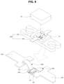
- FIGS. 8A and 8B are perspective views schematically illustrating a semiconductor package according to another embodiment of the present invention
- FIG. 9 is an exploded perspective view of the semiconductor package of FIGS. 8A and 8B
- FIGS. 10 through 12 are cross-sectional views of the semiconductor package of FIGS. 8A and 8B .
- the edge formed after the lower surface S 1 of the clip structure 300 meets the cut surface S 2 of the clip structure 300 may be adhered to face the upper surfaces of the chip pads 43 and 44 of the semiconductor chip 200 .
- a first angle ⁇ 1 between the upper surfaces of the chip pads 43 and 44 and the lower surface S 1 of the clip structure 300 and a second angle ⁇ 2 between the upper surfaces of the chip pads 43 and 44 and the cut surface S 2 of the clip structure 300 may be in the range of 10 to 85 degrees.
- the one end Q 1 of the clip structure 300 is electrically connected to the chip pads 43 and 44 and the other end of the clip structure 300 is electrically connected to the lead 104 .
- the clip structure 300 may be formed by bending.
- the lower surface S 1 and the cut surface S 2 incline at a regular angle in the edge and at least a part of a cross-section L 1 of the edge cut along a longitudinal direction of the edge may be formed to surface-contact the upper surfaces of the chip pads 43 and 44 of the semiconductor chip 200 .
- the cross-section L 1 formed by cutting the edge may be formed to contact an upper surface L 2 of the chip pad 43 and 44 of the semiconductor chip 200 in a width direction with the rate of 0.3 to 0.5:1.
- the lower surface S 1 and the cut surface S 2 incline at a regular angle in the edge and a cross-section of the edge cut along a longitudinal direction of the edge may be formed to be a chamfer. Then, the cross-section of the edge may contact the entire upper surface of the chip pads 43 and 44 of the semiconductor chip 200 .
- a part of the cross-section formed by cutting the clip structure 300 may only surface-contact the upper surfaces of the chip pads 43 and 44 or the entire cross-section may be chamfered to surface-contact the upper surfaces of the chip pads 43 and 44 .
- line-contact may be accomplished by the third adhesive layer 33 between a V shape or a U shape edge and the chip pads 41 and 42 .
- the one end Q 1 of the clip structure 300 may be electrically connected to the upper surfaces of the chip pads 43 and 44 of the semiconductor chip by using the third adhesive layer 33 as a medium.
- the conductive third adhesive layer 33 is interposed between the clip structure 300 and the chip pad 43 .
- the edge of the clip structure 300 is filled in the third adhesive layer 33 and thus, the lower surface S 1 , the cut surface S 2 , and at least a part of the cross-section of the edge cut along a longitudinal direction of the edge simultaneously contact the third adhesive layer 33 . Therefore, an electrical contact area between the clip structure 300 and the chip pads 41 and 42 may be sufficiently secured. Also, due to surface-contact between the clip structure 300 and the chip pads 43 and 44 , an electrical contact area may be sufficiently secured and a fixation area may be stably secured.
- the pad 103 may be a pad of a lead frame or a pad of a board and the lead 104 is a terminal lead.
- a lower ceramic case 51 is placed on the upper part of the pad 103 .
- the pad 103 and the lead 104 are spaced apart from each other in a regular interval by the lower ceramic case 51 .
- the semiconductor chip 200 is adhered to a part of the pad 103 exposed through an inner space of the lower ceramic case 51 by using a conductive adhesive 34 .
- the clip structure 300 is adhered to the semiconductor chip 200 and is protected by covering or molding an upper housing 52 on the upper part of the lower ceramic case 51 so that one end of the lead 104 is exposed to the outside.
- FIG. 13 is a perspective view schematically illustrating a semiconductor package 1001 according to another embodiment of the present invention
- FIG. 14 is a cross-sectional view of the semiconductor package 1001 cut along a line XIV-XIV of FIG. 13
- FIG. 15 is a perspective view of leads 700 included in the semiconductor package 1001 .
- the semiconductor package 1001 may be used as a power amplifier for base stations of mobile communication, a power amplifier for automobiles, marine radar, and a power amplifier for air traffic control radar and is not limited thereto.
- the semiconductor chip 600 includes a GaN semiconductor and may include a source, a GaN semiconductor layer, a gate, and a drain, wherein the source, the gate, the drain respectively include chip pads 511 for the source, the gate, and the drain.
- a size of the chip pad 511 may be 500 ⁇ m or below in width and 500 ⁇ m or below in length.
- the other end Q 20 of the lead 700 is exposed to the outside of the sealing member 800 , however, the present invention is not limited thereto.
- the Q 20 of the lead 700 may be disposed on a virtual plane that is the same as the side of the sealing member 800 (not illustrated).
- the first lead member 521 includes a flat part 521 a including the other end Q 20 of the lead 700 and a bending part 521 b connecting the flat part 521 a to the second lead member 522 .
- the bending part 521 b facilitates adhering of the second lead member 522 to the upper part of the chip pad 511 of the semiconductor chip 600 .
- An one end Q 10 of the second lead member 522 may incline and contact the other surface P 2 of the semiconductor chip 600 .
- the second lead member 522 inclines and contacts the upper surface of the chip pad 511 in such a way that an edge formed after an one surface S 10 of the second lead member 522 meets a cut surface S 20 of the second lead member 522 is adhered toward the upper surface of the chip pad 511 disposed on the other surface P 2 of the semiconductor chip 600 .
- the one surface S 10 of the second lead member 522 may be formed on a plane that is same as the one surface P 3 of the flat part 521 a and is a lower surface of the lead 700 .
- an interval between the one end Q 10 of the second lead member 522 that is, the edge formed after the one surface S 10 of the second lead member 522 meets the cut surface S 20 of the second lead member 522 , and the one surface of the chip pad 511 of the semiconductor chip 600 may be in the range of 0 to 70 um.
- a first angle ⁇ 10 between the upper surface of the chip pad 511 and the one surface S 10 of the second lead member 522 and a second angle ⁇ 20 between the upper surface of the chip pad 511 and the cut surface S 20 of the second lead member 522 may be in the range of 10 to 85 degrees.
- the one surface S 10 of the second lead member 522 or the cut surface S 20 of the second lead member 522 is formed to incline at a regular angle with respect to the upper surface of the chip pad 511 , the one end Q 10 of the second lead member 522 is partially embedded in the adhesive layer 530 interposed between the second lead member 522 and the chip pad 511 . Accordingly, even if the area of the chip pad 511 decreases, an inclined surface and the adhesive layer 530 formed on the one end Q 10 of the second lead member 522 may be sufficiently secure a contact surface and thereby, an adhesive force may increase.
- FIGS. 16 and 17 are respectively a picture illustrating one end of a lead adhered to an adhesive layer and its simulation view according to another embodiment of the present invention.
- the lead 700 inclines with respect to the upper surface of the chip pad 511 and the adhesive layer 530 contact the one surface S 10 and the cut surface S 2 of the lead 700 . Accordingly, a contact area may be sufficiently secured and thereby, the lead 700 may be stably fixed to the chip pad 511 .
- FIG. 18 is a perspective view schematically illustrating a semiconductor package 1002 according to another embodiment of the present invention and FIGS. 19 and 20 are cross-sectional views of the semiconductor package 1002 .
- the semiconductor package 1002 illustrated in FIGS. 18 through 20 is mostly similar to the semiconductor package 1001 illustrated in FIG. 13 and thus, only differences therebetween will be described in more detail.
- the semiconductor package 1002 of FIGS. 18 through 20 includes the semiconductor chip 600 and one or more leads 700 electrically connected to the semiconductor chip 600 .
- the one end Q 10 of the second lead member 522 contacts the one surface P 1 on the semiconductor chip 600 and thus, a part of the semiconductor chip 600 is exposed to a lower surface of the semiconductor package 1001 , that is the bottom surface.
- the semiconductor chip 600 contacts the one surface P 1 on the second lead member 522 and thus, a part of the semiconductor chip 600 is exposed to an upper surface of the semiconductor package 1002 .
- the first lead member 521 may only include a flat part without a bending part.
- the edge of the second lead member 522 may be bent toward the chip pad 511 .
- the edge formed after the one surface S 10 of the second lead member 522 meets the cut surface S 20 of the second lead member 522 may contact the chip pad 511 of the semiconductor chip 600 .
- the one surface S 10 of the second lead member 522 or the cut surface S 20 of the second lead member 522 may have an inclined surface inclined with respect to the one surface of the chip pad 511 .
- An angle between the inclined surface and the chip pad 511 may be in the range of 10 to 85 degrees.
- the second lead member 522 may be connected to the chip pad 511 through a projection 540 formed on the edge thereof without being bent or curved.
- the projection 540 may include an inclined surface SSS inclined with respect to the one surface of the chip pad 511 of the semiconductor chip 600 and a cross-section of the projection 540 may be a triangle.
- the one surface P 1 of the semiconductor chip 600 is exposed to the outside of the sealing member 800 .
- the one surface P 1 of the semiconductor chip 600 is not exposed to the outside of the sealing member 800 and instead, the one surface P 1 and the other surface P 2 may be simultaneously filled in the sealing member 800 (not illustrated).
- a number of the lead adhered to the semiconductor chip according to the embodiment of the present invention is one or more and more preferably, plural.
- the leads may be connected to each other.
- FIGS. 21 and 22 illustrate a method of manufacturing a semiconductor package according to another embodiment of the present invention.
- the semiconductor chip 600 including a GaN semiconductor and a lead member 710 including the plurality of leads 700 are prepared and the second lead member 522 is adhered on the chip pad of the semiconductor chip 600 through an adhesive layer.
- connection part 520 is cut and removed after the sealing member 800 is formed and thus, the ends of the first lead members 521 may be connected.
- the sealing member 800 is formed to surround the semiconductor chip 600 .
- the sealing member 800 is formed by using a well-known technology and thereby, detailed description of forming the sealing member 800 is omitted.
- the connection part 520 of the lead member 710 is exposed to the outside of the sealing member 800 .
- a trimming process is performed to remove the connection part 520 exposed to the outside of the sealing member 800 as in FIG. 13 , and to complete forming of the semiconductor package.
- a clip may be easily adhered to a pad area, even if a size of the pad area becomes smaller, and a sufficient adhesive force between the clip and the pad area may maintain.
- a size of a pad area may be minimized and thereby, a communication property may be improved.
- a lead may be easily adhered to a chip pad, even if a size of the chip pad becomes smaller, and a sufficient adhesive force between the lead and the chip pad may maintain.
- the semiconductor package according to another embodiment of the present invention when applied to a semiconductor package including a GaN material used in communication, a size of a chip pad may be minimized and thereby, a communication property may be improved.
Abstract
Description
Claims (18)
Priority Applications (1)
| Application Number | Priority Date | Filing Date | Title |
|---|---|---|---|
| US17/580,598 US11676931B2 (en) | 2019-06-04 | 2022-01-20 | Semiconductor package |
Applications Claiming Priority (6)
| Application Number | Priority Date | Filing Date | Title |
|---|---|---|---|
| KR10-2019-0066172 | 2019-06-04 | ||
| KR20190066172 | 2019-06-04 | ||
| KR10-2019-0079889 | 2019-07-03 | ||
| KR1020190079889A KR102327950B1 (en) | 2019-07-03 | 2019-07-03 | Semiconductor package |
| KR10-2020-0017842 | 2020-02-13 | ||
| KR1020200017842A KR102343920B1 (en) | 2019-06-04 | 2020-02-13 | Semiconductor package |
Related Child Applications (1)
| Application Number | Title | Priority Date | Filing Date |
|---|---|---|---|
| US17/580,598 Continuation US11676931B2 (en) | 2019-06-04 | 2022-01-20 | Semiconductor package |
Publications (2)
| Publication Number | Publication Date |
|---|---|
| US20200388588A1 US20200388588A1 (en) | 2020-12-10 |
| US11270969B2 true US11270969B2 (en) | 2022-03-08 |
Family
ID=73650762
Family Applications (2)
| Application Number | Title | Priority Date | Filing Date |
|---|---|---|---|
| US16/847,696 Active 2040-04-19 US11270969B2 (en) | 2019-06-04 | 2020-04-14 | Semiconductor package |
| US17/580,598 Active US11676931B2 (en) | 2019-06-04 | 2022-01-20 | Semiconductor package |
Family Applications After (1)
| Application Number | Title | Priority Date | Filing Date |
|---|---|---|---|
| US17/580,598 Active US11676931B2 (en) | 2019-06-04 | 2022-01-20 | Semiconductor package |
Country Status (1)
| Country | Link |
|---|---|
| US (2) | US11270969B2 (en) |
Cited By (2)
| Publication number | Priority date | Publication date | Assignee | Title |
|---|---|---|---|---|
| US20220148998A1 (en) * | 2019-06-04 | 2022-05-12 | Jmj Korea Co., Ltd. | Semiconductor package |
| US20220221353A1 (en) * | 2021-01-12 | 2022-07-14 | Texas Instruments Incorporated | Semiconductor force sensors |
Families Citing this family (3)
| Publication number | Priority date | Publication date | Assignee | Title |
|---|---|---|---|---|
| EP3703121B1 (en) * | 2017-10-26 | 2022-08-10 | Shindengen Electric Manufacturing Co., Ltd. | Semiconductor device and method for manufacturing semiconductor device |
| CN216054684U (en) * | 2019-03-25 | 2022-03-15 | 新电元工业株式会社 | Semiconductor device, lead frame and power supply device |
| TWI776739B (en) * | 2021-11-23 | 2022-09-01 | 南茂科技股份有限公司 | Chip package structure |
Citations (15)
| Publication number | Priority date | Publication date | Assignee | Title |
|---|---|---|---|---|
| JP2574510B2 (en) | 1989-04-17 | 1997-01-22 | 松下電器産業株式会社 | High frequency semiconductor device |
| KR20010111736A (en) | 2000-06-13 | 2001-12-20 | 김덕중 | Power module package having a insulator type heat sink attached a backside of leadframe & manufacturing method thereof |
| KR100685253B1 (en) | 1998-07-31 | 2007-02-22 | 익시스 코포레이션 | Electrically isolated power semiconductor package |
| KR20080038180A (en) | 2005-08-30 | 2008-05-02 | 페어차일드 세미컨덕터 코포레이션 | Reversible-multiple footprint package and method of manufacturing |
| US7525184B2 (en) * | 2002-07-01 | 2009-04-28 | Renesas Technology Corp. | Semiconductor device and its manufacturing method |
| JP2013219373A (en) | 2000-12-28 | 2013-10-24 | Renesas Electronics Corp | Semiconductor device |
| KR20140073241A (en) | 2012-12-06 | 2014-06-16 | 주식회사 케이이씨 | Semiconductor package and fabricating method thereof |
| JP2014143326A (en) | 2013-01-24 | 2014-08-07 | Transphorm Japan Inc | Semiconductor device, method of manufacturing semiconductor device, lead, and method of manufacturing lead |
| JP2014192292A (en) | 2013-03-27 | 2014-10-06 | Rohm Co Ltd | Semiconductor device and semiconductor device manufacturing method |
| JP2015012065A (en) | 2013-06-27 | 2015-01-19 | 株式会社デンソー | Method of manufacturing semiconductor device |
| US20150155227A1 (en) * | 2011-02-14 | 2015-06-04 | Renesas Electronics Corporation | Semiconductor device |
| KR20160033870A (en) | 2014-09-18 | 2016-03-29 | 제엠제코(주) | Semiconductor package with clip structure |
| US9704797B2 (en) * | 2011-05-18 | 2017-07-11 | Sandisk Information Technology (Shanghai) Co., Ltd. | Waterfall wire bonding |
| US10366958B2 (en) * | 2017-12-28 | 2019-07-30 | Texas Instruments Incorporated | Wire bonding between isolation capacitors for multichip modules |
| US10692917B2 (en) * | 2016-07-06 | 2020-06-23 | Kingpak Technology Inc. | Sensor package structure |
Family Cites Families (4)
| Publication number | Priority date | Publication date | Assignee | Title |
|---|---|---|---|---|
| US7057273B2 (en) * | 2001-05-15 | 2006-06-06 | Gem Services, Inc. | Surface mount package |
| WO2011155165A1 (en) * | 2010-06-11 | 2011-12-15 | パナソニック株式会社 | Resin-sealed semiconductor device and method for manufacturing same |
| WO2019038876A1 (en) * | 2017-08-24 | 2019-02-28 | 新電元工業株式会社 | Semiconductor device |
| US11270969B2 (en) * | 2019-06-04 | 2022-03-08 | Jmj Korea Co., Ltd. | Semiconductor package |
-
2020
- 2020-04-14 US US16/847,696 patent/US11270969B2/en active Active
-
2022
- 2022-01-20 US US17/580,598 patent/US11676931B2/en active Active
Patent Citations (15)
| Publication number | Priority date | Publication date | Assignee | Title |
|---|---|---|---|---|
| JP2574510B2 (en) | 1989-04-17 | 1997-01-22 | 松下電器産業株式会社 | High frequency semiconductor device |
| KR100685253B1 (en) | 1998-07-31 | 2007-02-22 | 익시스 코포레이션 | Electrically isolated power semiconductor package |
| KR20010111736A (en) | 2000-06-13 | 2001-12-20 | 김덕중 | Power module package having a insulator type heat sink attached a backside of leadframe & manufacturing method thereof |
| JP2013219373A (en) | 2000-12-28 | 2013-10-24 | Renesas Electronics Corp | Semiconductor device |
| US7525184B2 (en) * | 2002-07-01 | 2009-04-28 | Renesas Technology Corp. | Semiconductor device and its manufacturing method |
| KR20080038180A (en) | 2005-08-30 | 2008-05-02 | 페어차일드 세미컨덕터 코포레이션 | Reversible-multiple footprint package and method of manufacturing |
| US20150155227A1 (en) * | 2011-02-14 | 2015-06-04 | Renesas Electronics Corporation | Semiconductor device |
| US9704797B2 (en) * | 2011-05-18 | 2017-07-11 | Sandisk Information Technology (Shanghai) Co., Ltd. | Waterfall wire bonding |
| KR20140073241A (en) | 2012-12-06 | 2014-06-16 | 주식회사 케이이씨 | Semiconductor package and fabricating method thereof |
| JP2014143326A (en) | 2013-01-24 | 2014-08-07 | Transphorm Japan Inc | Semiconductor device, method of manufacturing semiconductor device, lead, and method of manufacturing lead |
| JP2014192292A (en) | 2013-03-27 | 2014-10-06 | Rohm Co Ltd | Semiconductor device and semiconductor device manufacturing method |
| JP2015012065A (en) | 2013-06-27 | 2015-01-19 | 株式会社デンソー | Method of manufacturing semiconductor device |
| KR20160033870A (en) | 2014-09-18 | 2016-03-29 | 제엠제코(주) | Semiconductor package with clip structure |
| US10692917B2 (en) * | 2016-07-06 | 2020-06-23 | Kingpak Technology Inc. | Sensor package structure |
| US10366958B2 (en) * | 2017-12-28 | 2019-07-30 | Texas Instruments Incorporated | Wire bonding between isolation capacitors for multichip modules |
Cited By (3)
| Publication number | Priority date | Publication date | Assignee | Title |
|---|---|---|---|---|
| US20220148998A1 (en) * | 2019-06-04 | 2022-05-12 | Jmj Korea Co., Ltd. | Semiconductor package |
| US11676931B2 (en) * | 2019-06-04 | 2023-06-13 | Jmj Korea Co., Ltd. | Semiconductor package |
| US20220221353A1 (en) * | 2021-01-12 | 2022-07-14 | Texas Instruments Incorporated | Semiconductor force sensors |
Also Published As
| Publication number | Publication date |
|---|---|
| US20220148998A1 (en) | 2022-05-12 |
| US11676931B2 (en) | 2023-06-13 |
| US20200388588A1 (en) | 2020-12-10 |
Similar Documents
| Publication | Publication Date | Title |
|---|---|---|
| US11270969B2 (en) | Semiconductor package | |
| US6507093B2 (en) | Lead frame for fabricating surface mount type semiconductor devices with high reliability | |
| KR950012921B1 (en) | Plastic mold semiconductor device | |
| US9847282B2 (en) | Semiconductor device | |
| JP4686248B2 (en) | Optical semiconductor device and optical semiconductor device manufacturing method | |
| JP2005057067A (en) | Semiconductor device and manufacturing method thereof | |
| US8742552B2 (en) | Semiconductor device | |
| JP2007049045A (en) | Semiconductor light emitting device and semiconductor device using the same | |
| JP2023073509A (en) | Semiconductor device | |
| KR100813623B1 (en) | Flexible film semiconductor package and method for manufacturing the same | |
| JP2019121698A (en) | Semiconductor device and method for manufacturing semiconductor device | |
| US11776891B2 (en) | Semiconductor device | |
| US7534661B2 (en) | Method of forming molded resin semiconductor device | |
| JPH1174439A (en) | Resin mold package | |
| JPH07147360A (en) | Surface mounting type semiconductor device | |
| JPH07147359A (en) | Surface mounting type semiconductor device | |
| KR102327950B1 (en) | Semiconductor package | |
| JP2004047715A (en) | Semiconductor connection relay member and semiconductor device | |
| JP4531073B2 (en) | Semiconductor device | |
| KR102343920B1 (en) | Semiconductor package | |
| JP2533011B2 (en) | Surface mount semiconductor device | |
| EP0849794A1 (en) | Fine pitch lead frame | |
| JP2538407B2 (en) | Surface mount semiconductor device | |
| KR100253298B1 (en) | A semiconductor package with improved solder joint reliability and a device using the same | |
| JP2023179984A (en) | Lead frame and electronic component |
Legal Events
| Date | Code | Title | Description |
|---|---|---|---|
| AS | Assignment |
Owner name: JMJ KOREA CO., LTD., KOREA, REPUBLIC OF Free format text: ASSIGNMENT OF ASSIGNORS INTEREST;ASSIGNORS:CHOI, YUN HWA;CHO, JEONGHUN;KIM, YOUNG HUN;AND OTHERS;REEL/FRAME:052385/0793 Effective date: 20200413 |
|
| FEPP | Fee payment procedure |
Free format text: ENTITY STATUS SET TO UNDISCOUNTED (ORIGINAL EVENT CODE: BIG.); ENTITY STATUS OF PATENT OWNER: SMALL ENTITY |
|
| FEPP | Fee payment procedure |
Free format text: ENTITY STATUS SET TO SMALL (ORIGINAL EVENT CODE: SMAL); ENTITY STATUS OF PATENT OWNER: SMALL ENTITY |
|
| STPP | Information on status: patent application and granting procedure in general |
Free format text: DOCKETED NEW CASE - READY FOR EXAMINATION |
|
| STPP | Information on status: patent application and granting procedure in general |
Free format text: NON FINAL ACTION MAILED |
|
| STPP | Information on status: patent application and granting procedure in general |
Free format text: FINAL REJECTION MAILED |
|
| STPP | Information on status: patent application and granting procedure in general |
Free format text: DOCKETED NEW CASE - READY FOR EXAMINATION |
|
| STPP | Information on status: patent application and granting procedure in general |
Free format text: NOTICE OF ALLOWANCE MAILED -- APPLICATION RECEIVED IN OFFICE OF PUBLICATIONS |
|
| STPP | Information on status: patent application and granting procedure in general |
Free format text: AWAITING TC RESP., ISSUE FEE NOT PAID |
|
| STCF | Information on status: patent grant |
Free format text: PATENTED CASE |