JP2015012065A - Method of manufacturing semiconductor device - Google Patents
Method of manufacturing semiconductor device Download PDFInfo
- Publication number
- JP2015012065A JP2015012065A JP2013134965A JP2013134965A JP2015012065A JP 2015012065 A JP2015012065 A JP 2015012065A JP 2013134965 A JP2013134965 A JP 2013134965A JP 2013134965 A JP2013134965 A JP 2013134965A JP 2015012065 A JP2015012065 A JP 2015012065A
- Authority
- JP
- Japan
- Prior art keywords
- semiconductor chip
- solder
- clip
- bonded
- bonded portion
- Prior art date
- Legal status (The legal status is an assumption and is not a legal conclusion. Google has not performed a legal analysis and makes no representation as to the accuracy of the status listed.)
- Pending
Links
Images


Classifications
-
- H—ELECTRICITY
- H01—ELECTRIC ELEMENTS
- H01L—SEMICONDUCTOR DEVICES NOT COVERED BY CLASS H10
- H01L24/00—Arrangements for connecting or disconnecting semiconductor or solid-state bodies; Methods or apparatus related thereto
- H01L24/01—Means for bonding being attached to, or being formed on, the surface to be connected, e.g. chip-to-package, die-attach, "first-level" interconnects; Manufacturing methods related thereto
- H01L24/34—Strap connectors, e.g. copper straps for grounding power devices; Manufacturing methods related thereto
- H01L24/36—Structure, shape, material or disposition of the strap connectors prior to the connecting process
- H01L24/37—Structure, shape, material or disposition of the strap connectors prior to the connecting process of an individual strap connector
-
- H—ELECTRICITY
- H01—ELECTRIC ELEMENTS
- H01L—SEMICONDUCTOR DEVICES NOT COVERED BY CLASS H10
- H01L24/00—Arrangements for connecting or disconnecting semiconductor or solid-state bodies; Methods or apparatus related thereto
- H01L24/01—Means for bonding being attached to, or being formed on, the surface to be connected, e.g. chip-to-package, die-attach, "first-level" interconnects; Manufacturing methods related thereto
- H01L24/34—Strap connectors, e.g. copper straps for grounding power devices; Manufacturing methods related thereto
- H01L24/39—Structure, shape, material or disposition of the strap connectors after the connecting process
- H01L24/40—Structure, shape, material or disposition of the strap connectors after the connecting process of an individual strap connector
-
- H—ELECTRICITY
- H01—ELECTRIC ELEMENTS
- H01L—SEMICONDUCTOR DEVICES NOT COVERED BY CLASS H10
- H01L24/00—Arrangements for connecting or disconnecting semiconductor or solid-state bodies; Methods or apparatus related thereto
- H01L24/80—Methods for connecting semiconductor or other solid state bodies using means for bonding being attached to, or being formed on, the surface to be connected
- H01L24/84—Methods for connecting semiconductor or other solid state bodies using means for bonding being attached to, or being formed on, the surface to be connected using a strap connector
-
- H—ELECTRICITY
- H01—ELECTRIC ELEMENTS
- H01L—SEMICONDUCTOR DEVICES NOT COVERED BY CLASS H10
- H01L2224/00—Indexing scheme for arrangements for connecting or disconnecting semiconductor or solid-state bodies and methods related thereto as covered by H01L24/00
- H01L2224/01—Means for bonding being attached to, or being formed on, the surface to be connected, e.g. chip-to-package, die-attach, "first-level" interconnects; Manufacturing methods related thereto
- H01L2224/26—Layer connectors, e.g. plate connectors, solder or adhesive layers; Manufacturing methods related thereto
- H01L2224/31—Structure, shape, material or disposition of the layer connectors after the connecting process
- H01L2224/32—Structure, shape, material or disposition of the layer connectors after the connecting process of an individual layer connector
- H01L2224/321—Disposition
- H01L2224/32151—Disposition the layer connector connecting between a semiconductor or solid-state body and an item not being a semiconductor or solid-state body, e.g. chip-to-substrate, chip-to-passive
- H01L2224/32221—Disposition the layer connector connecting between a semiconductor or solid-state body and an item not being a semiconductor or solid-state body, e.g. chip-to-substrate, chip-to-passive the body and the item being stacked
- H01L2224/32245—Disposition the layer connector connecting between a semiconductor or solid-state body and an item not being a semiconductor or solid-state body, e.g. chip-to-substrate, chip-to-passive the body and the item being stacked the item being metallic
-
- H—ELECTRICITY
- H01—ELECTRIC ELEMENTS
- H01L—SEMICONDUCTOR DEVICES NOT COVERED BY CLASS H10
- H01L2224/00—Indexing scheme for arrangements for connecting or disconnecting semiconductor or solid-state bodies and methods related thereto as covered by H01L24/00
- H01L2224/01—Means for bonding being attached to, or being formed on, the surface to be connected, e.g. chip-to-package, die-attach, "first-level" interconnects; Manufacturing methods related thereto
- H01L2224/34—Strap connectors, e.g. copper straps for grounding power devices; Manufacturing methods related thereto
- H01L2224/39—Structure, shape, material or disposition of the strap connectors after the connecting process
- H01L2224/40—Structure, shape, material or disposition of the strap connectors after the connecting process of an individual strap connector
- H01L2224/4005—Shape
- H01L2224/4009—Loop shape
- H01L2224/40095—Kinked
-
- H—ELECTRICITY
- H01—ELECTRIC ELEMENTS
- H01L—SEMICONDUCTOR DEVICES NOT COVERED BY CLASS H10
- H01L2224/00—Indexing scheme for arrangements for connecting or disconnecting semiconductor or solid-state bodies and methods related thereto as covered by H01L24/00
- H01L2224/01—Means for bonding being attached to, or being formed on, the surface to be connected, e.g. chip-to-package, die-attach, "first-level" interconnects; Manufacturing methods related thereto
- H01L2224/34—Strap connectors, e.g. copper straps for grounding power devices; Manufacturing methods related thereto
- H01L2224/39—Structure, shape, material or disposition of the strap connectors after the connecting process
- H01L2224/40—Structure, shape, material or disposition of the strap connectors after the connecting process of an individual strap connector
- H01L2224/401—Disposition
- H01L2224/40135—Connecting between different semiconductor or solid-state bodies, i.e. chip-to-chip
- H01L2224/40137—Connecting between different semiconductor or solid-state bodies, i.e. chip-to-chip the bodies being arranged next to each other, e.g. on a common substrate
-
- H—ELECTRICITY
- H01—ELECTRIC ELEMENTS
- H01L—SEMICONDUCTOR DEVICES NOT COVERED BY CLASS H10
- H01L2224/00—Indexing scheme for arrangements for connecting or disconnecting semiconductor or solid-state bodies and methods related thereto as covered by H01L24/00
- H01L2224/01—Means for bonding being attached to, or being formed on, the surface to be connected, e.g. chip-to-package, die-attach, "first-level" interconnects; Manufacturing methods related thereto
- H01L2224/34—Strap connectors, e.g. copper straps for grounding power devices; Manufacturing methods related thereto
- H01L2224/39—Structure, shape, material or disposition of the strap connectors after the connecting process
- H01L2224/40—Structure, shape, material or disposition of the strap connectors after the connecting process of an individual strap connector
- H01L2224/401—Disposition
- H01L2224/40151—Connecting between a semiconductor or solid-state body and an item not being a semiconductor or solid-state body, e.g. chip-to-substrate, chip-to-passive
- H01L2224/40221—Connecting between a semiconductor or solid-state body and an item not being a semiconductor or solid-state body, e.g. chip-to-substrate, chip-to-passive the body and the item being stacked
- H01L2224/40245—Connecting between a semiconductor or solid-state body and an item not being a semiconductor or solid-state body, e.g. chip-to-substrate, chip-to-passive the body and the item being stacked the item being metallic
-
- H—ELECTRICITY
- H01—ELECTRIC ELEMENTS
- H01L—SEMICONDUCTOR DEVICES NOT COVERED BY CLASS H10
- H01L2224/00—Indexing scheme for arrangements for connecting or disconnecting semiconductor or solid-state bodies and methods related thereto as covered by H01L24/00
- H01L2224/80—Methods for connecting semiconductor or other solid state bodies using means for bonding being attached to, or being formed on, the surface to be connected
- H01L2224/83—Methods for connecting semiconductor or other solid state bodies using means for bonding being attached to, or being formed on, the surface to be connected using a layer connector
- H01L2224/838—Bonding techniques
- H01L2224/83801—Soldering or alloying
-
- H—ELECTRICITY
- H01—ELECTRIC ELEMENTS
- H01L—SEMICONDUCTOR DEVICES NOT COVERED BY CLASS H10
- H01L2224/00—Indexing scheme for arrangements for connecting or disconnecting semiconductor or solid-state bodies and methods related thereto as covered by H01L24/00
- H01L2224/80—Methods for connecting semiconductor or other solid state bodies using means for bonding being attached to, or being formed on, the surface to be connected
- H01L2224/84—Methods for connecting semiconductor or other solid state bodies using means for bonding being attached to, or being formed on, the surface to be connected using a strap connector
- H01L2224/848—Bonding techniques
- H01L2224/84801—Soldering or alloying
-
- H—ELECTRICITY
- H01—ELECTRIC ELEMENTS
- H01L—SEMICONDUCTOR DEVICES NOT COVERED BY CLASS H10
- H01L2924/00—Indexing scheme for arrangements or methods for connecting or disconnecting semiconductor or solid-state bodies as covered by H01L24/00
- H01L2924/0001—Technical content checked by a classifier
- H01L2924/00014—Technical content checked by a classifier the subject-matter covered by the group, the symbol of which is combined with the symbol of this group, being disclosed without further technical details
-
- H—ELECTRICITY
- H01—ELECTRIC ELEMENTS
- H01L—SEMICONDUCTOR DEVICES NOT COVERED BY CLASS H10
- H01L2924/00—Indexing scheme for arrangements or methods for connecting or disconnecting semiconductor or solid-state bodies as covered by H01L24/00
- H01L2924/15—Details of package parts other than the semiconductor or other solid state devices to be connected
- H01L2924/181—Encapsulation
Abstract
Description
本発明は、はんだ接合により、リードフレームや配線基板等に半導体チップ等を実装した半導体装置の製造方法に関する。 The present invention relates to a method for manufacturing a semiconductor device in which a semiconductor chip or the like is mounted on a lead frame, a wiring board, or the like by solder bonding.
従来、はんだ接合により、リードフレーム等に半導体チップ等を接合して構成される半導体装置が知られている。この種の半導体装置の製造方法では、一般に、はんだが加熱により溶融する際に、空気を巻き込むことや、はんだがフラックスを含有する場合にはフラックスが分解ガスを発生させることにより、はんだにこれらの気体が残留してボイドが形成される。はんだにボイドが形成されると、半導体装置の接合強度や放熱性等の性能が不十分となり得るため、好ましくない。 2. Description of the Related Art Conventionally, a semiconductor device configured by bonding a semiconductor chip or the like to a lead frame or the like by solder bonding is known. In this type of semiconductor device manufacturing method, generally, when the solder is melted by heating, air is entrained, or when the solder contains a flux, the flux generates a decomposition gas. Gas remains and voids are formed. If voids are formed in the solder, the performance of the semiconductor device, such as the bonding strength and heat dissipation, may be insufficient.
はんだにおけるボイド形成を抑制する技術として、特許文献1に記載の方法が提案されている。この方法では、はんだ接合によって、リードフレームを基板に接合する際に、この方法では、リードフレームに貫通孔を設け、この貫通孔からはんだ溶融時に生じる気体を放出することにより、はんだにおけるボイド形成を抑制している。
As a technique for suppressing void formation in solder, a method described in
上記の特許文献1の方法では、ボイド抑制効果を高めるためには、リードフレームに設ける貫通孔を大きくしなければならない。しかしながら、リードフレームの強度等の問題から、貫通孔の大きさは制限される。このため、上記の特許文献1の方法では、十分なボイド抑制効果を得ることが難しい。また、上記の特許文献1の方法では、貫通孔を形成することが困難なもの(幅が短いなど孔加工をすることが困難なリードフレームなど)には適用できない。
In the method disclosed in
本発明は上記点に鑑みて、はんだ接合された部分を有する半導体装置の製造方法において、上述した貫通孔を形成することなく、はんだにおけるボイド形成が抑制される製造方法を提供することを目的とする。 In view of the above points, an object of the present invention is to provide a manufacturing method in which void formation in solder is suppressed without forming the above-described through hole in a manufacturing method of a semiconductor device having a soldered portion. To do.
上記目的を達成するため、請求項1に記載の発明では、第1のはんだ(5)により第1の被接合部(21)と半導体チップ(3)とを接合して構成される半導体装置の製造方法において、半導体チップの重心から離れた位置に荷重を加えることにより、第1のはんだを溶融させてからその固化が完了するまで、半導体チップの一面(3a)を、第1の被接合部の一面(21a)に対して傾斜した状態に維持することを特徴とする。 In order to achieve the above object, according to the first aspect of the present invention, there is provided a semiconductor device configured by joining the first joined portion (21) and the semiconductor chip (3) with the first solder (5). In the manufacturing method, by applying a load to a position away from the center of gravity of the semiconductor chip, the first surface (3a) of the semiconductor chip is melted until the solidification is completed after the first solder is melted. It maintains in the state inclined with respect to one surface (21a).
このため、溶融状態の第1のはんだ中に存在する気体(例えば、フラックスが分解して発生するガス)が、第1の被接合部の一面と半導体チップの一面との間隔が広い領域において移動し易くなる。よって、この広い領域を通じて気体が第1のはんだの外部へ放出され易くなり、固化後における第1のはんだ中にボイドが形成され難くなる。これにより、貫通孔を形成しなくても、はんだにおけるボイド形成を抑制することが可能となる。 For this reason, the gas (for example, gas generated when the flux is decomposed) present in the molten first solder moves in a region where the distance between one surface of the first bonded portion and one surface of the semiconductor chip is wide. It becomes easy to do. Therefore, gas is easily released to the outside of the first solder through this wide region, and voids are hardly formed in the first solder after solidification. This makes it possible to suppress void formation in the solder without forming a through hole.
なお、この欄および特許請求の範囲で記載した各手段の括弧内の符号は、後述する実施形態に記載の具体的手段との対応関係を示すものである。 In addition, the code | symbol in the bracket | parenthesis of each means described in this column and the claim shows the correspondence with the specific means as described in embodiment mentioned later.
以下、本発明の実施形態について図に基づいて説明する。なお、以下の各実施形態相互において、互いに同一もしくは均等である部分には、同一符号を付して説明を行う。 Hereinafter, embodiments of the present invention will be described with reference to the drawings. In the following embodiments, parts that are the same or equivalent to each other will be described with the same reference numerals.
(第1実施形態)
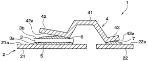
本発明の第1実施形態に係る半導体装置1について図1を参照して説明する。本実施形態に係る半導体装置1は、例えば自動車などの車両に搭載され、車両用の各種電子装置を駆動するための装置として適用される。
(First embodiment)
A
図1(a)、(b)に示すように、本実施形態に係る半導体装置1は、アイランド部21およびリード部22により構成されるリードフレーム2と、半導体チップ3と、半導体チップ3とリード部22とに接合されたクリップ4と、を備える。本実施形態に係る半導体装置1は、半導体チップ3が、第1のはんだ5を介してアイランド部21に接合され、クリップ4が、第2のはんだ6を介して半導体チップ3に接合される共に、第3のはんだ7を介してリード部22に接合された構成とされている。
As shown in FIGS. 1A and 1B, the
リードフレーム2は、導電性金属材料よりなるものであり、上述したように、 アイランド部(第1の被接合部)21およびリード部(第2の被接合部)22により構成される。アイランド部21は、半導体チップ3を積載するための薄板部材である。リード部22は、アイランド部21の周囲に配置された薄板部材である。リード部22は、クリップ4を介して半導体チップ3と電気的に接続されていると共に、図示しない配線により半導体装置1の外部と電気的に接続されている。
The
半導体チップ3は、平板状に形成された半導体集積回路であり、例えば、マイコンなどのICチップや、トランジスタなどのパワー素子や、その他の各種チップ部品等により構成される。
The
図1(a)に示すように、半導体チップ3は、その一面3aがアイランド部21の一面21aに対向するようにして配置されている。アイランド部21の一面21aと半導体チップ3の一面3aとの間には、半導体チップ3の一面3aの略全面に亘って、第1のはんだ5が設けられている。本実施形態に係る半導体装置1では、第1のはんだ5により、アイランド部21と半導体チップ3とが接合されている。
As shown in FIG. 1A, the
図1(a)に示すように、本実施形態に係る半導体装置1は、半導体チップ3の一面3aが、アイランド部21の一面21aに対して傾斜した傾斜状態とされた構成とされている。
As shown in FIG. 1A, the
クリップ4は、半導体チップ3とリード部22に接合されたものであり、金属(例えば、Cu)よりなる。図1(a)、(b)に示すように、クリップ4は、例えば板状部材を4箇所で折り曲げて形成され、両端の間に凸部41を備えた形状とされている。すなわち、クリップ4は、凸部41と、凸部41を挟んだ両端の部分のうちの一方の端部である第1部位42、および他方の端部である第2部位43と、を有して構成されている。また、本実施形態に係る半導体装置1は、クリップ4のうち第1部位42と凸部41との境界位置が、半導体チップ3の重心よりもリード部22の側に配置された構成とされている。
The
第1部位42は一面(第1の面)42aを有し、第2部位43は一面(第2の面)43aを有する。図1(a)に示すように、クリップ4の第1部位42の一面42aは、半導体チップ3のうち一面3aとは反対側の他面3bと、第2のはんだ6を介して接合されている。第2のはんだ6は、クリップ4の第1部位42の一面42aの略全面に亘って設けられている。
The
また、図1(a)に示すように、クリップ4の第2部位43の一面43aは、第3のはんだ7を介してリード部22の一面22aと接合されている。第3のはんだ7は、クリップ4の第2部位43の一面43aの略全面に亘って設けられている。このような構成により、クリップ4にて、半導体チップ3とリード部22とが物理的および電気的に接続されている。
Further, as shown in FIG. 1A, the one
本実施形態に係る半導体装置1では、クリップ4の第1部位42の一面42aが、半導体チップ3の他面3bに対して傾斜した傾斜状態となっている。また、本実施形態に係る半導体装置1では、クリップ4の第2部位43の一面43aが、リード部22の一面22aに対して傾斜した傾斜状態となっている。また、図1(a)に示すように、本実施形態に係る半導体装置1では、第1部位42の一面42aを含む平面と、第2部位43の一面43aを含む平面とが交差するように、第1部位42の一面42aおよび第2部位43の一面43aが設けられている。
In the
なお、本実施形態に係る半導体装置1では、リード部22のうち一部(外部と電気的に接続する配線が設けられる部分)を除いた部分、半導体チップ3、およびクリップ4が、図示しない被覆部(モールド樹脂など)により被覆されている。
In the
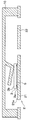
次に、本実施形態に係る半導体装置1の製造方法について、図2〜3を参照して説明する。
Next, a method for manufacturing the
まず、用意工程として、リードフレーム2(アイランド部21、リード部22)、半導体チップ3、およびクリップ4を用意する。
First, as a preparation process, the lead frame 2 (the
用意工程ののち、積載工程を行う。具体的には、まず最初に、半導体チップ3の一面3aがアイランド部21の一面21aに対向するように半導体チップ3をアイランド部21上に積載して、半導体チップ3の一面3aとアイランド部21の一面21aとを第1のはんだ5を介して接着させる。次に、クリップ4の第1部位42の一面42aが半導体チップ3の他面3bに対向すると共に、クリップ4の第2部位43の一面43aがリード部22の一面22aに対向するように、クリップ4を半導体チップ3上およびリード部22上に積載する。このとき、クリップ4のうち第1部位42と凸部41との境界位置が、半導体チップ3の重心よりもリード部22の側に配置されるように、クリップ4を半導体チップ3上およびリード部22上に積載する。そして、クリップ4の第1部位42の一面42aと半導体チップ3の他面3bとを第2のはんだ6を介して接着させ、第2部位43の一面43aとリード部22の一面22aとを第3のはんだ7を介して接着させる。
After the preparation process, the loading process is performed. Specifically, first, the
第1のはんだ5、第2のはんだ6、第3のはんだ7としては、それぞれ、例えばフラックスを含有するはんだが採用され得る。
As the
積載工程が完了したとき(はんだ溶融前)のワークは、図2に示すように、半導体チップ3の一面3aおよび他面3bがそれぞれ、アイランド部21の一面21aと略平行の状態となる。
As shown in FIG. 2, when the loading process is completed (before solder melting), the one
また、ワークは、クリップ4の第1部位42の一面42aが、アイランド部21の一面21aに対して傾斜した状態、すなわち、半導体チップ3の他面3bに対して傾斜した状態となる。より具体的には、第1部位42の一面42aは、第1部位42と凸部41との境界位置から第1部位42の端部側に向かうにつれてこの一面42aと半導体チップ3の他面3bとの間隔が広くなるように、傾斜する。また、上記境界位置が、半導体チップ3の重心よりもリード部22の側において配置された状態とされている。
Further, the work is in a state where one
さらに、ワークは、クリップ4の第2部位43の一面43aが、リード部22の一面22aに対して傾斜した状態となる。より具体的には、第2部位43の一面43aは、第2部位43と凸部41との境界位置から第2部位43の端部側に向かうにつれてこの第2部位43の一面43aとリード部22の一面22aとの間隔が広くなるように、傾斜する。
Furthermore, the workpiece is in a state in which the one
ここで、ワークにおいて、クリップ4が上述した形状とされているため、クリップ4の自重は、クリップ4のうち第1部位42と凸部41との境界位置の部分、および、クリップ4のうち凸部41と第2部位43との境界位置の部分に集中する。このクリップ4の自重が集中する2つの境界位置の一方である第1部位42と凸部41との境界位置は、上述したように、半導体チップ3の重心よりもリード部22の側に配置された状態とされている。このため、積載完了時におけるワークは、半導体チップ3の他面3bのうち半導体チップ3の重心から離れた位置に荷重(クリップ4の自重)が加えられた状態とされている。
Here, in the workpiece, since the
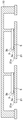
積載工程ののち、傾斜工程を行う。具体的には、第1のはんだ5、第2のはんだ6、および第3のはんだ7を溶融させることで、半導体チップ3およびクリップ4を図1に示すような状態にする。
After the loading process, the tilting process is performed. Specifically, by melting the
すなわち、第1のはんだ5を溶融させたときに、上述したように、半導体チップ3の他面3bのうち半導体チップ3の重心から離れた位置に荷重が加えられるため、半導体チップ3の一面3aがアイランド部21の一面21aに対して傾斜した状態となる。より具体的には、第1部位42の一面42aと半導体チップ3の他面3bとの間隔が広くなる方向に向かうにつれて、半導体チップ3とアイランド部21との間隔が広くなるように、半導体チップ3の一面3aがアイランド部21の一面21aに対して傾斜する。また、クリップ4の第1部位42の一面42aは、半導体チップ3が上述したように傾斜してもなお、はんだ溶融前と同様、半導体チップ3の他面3bに対して傾斜した状態を維持する。また、クリップ4の第2部位43の一面43aも、はんだ溶融前と同様、リード部22の一面22aに対して傾斜した状態を維持する。
That is, when the
なお、傾斜工程において、別途の外力(例えば、加圧機による圧力)を作用させることにより、さらに半導体チップ3が傾斜し易くなるようにしてもよい。
In the tilting step, the
傾斜工程ののち、固化工程として、半導体チップ3の一面3a、クリップ4の第1部位42の一面42a、およびクリップ4の第2部位43の一面43aのそれぞれの傾斜状態を維持した状態で、第1のはんだ5、第2のはんだ6、および第3のはんだ7の固化を完了させる。
After the tilting process, as the solidification process, the
以上のような製造方法により、本実施形態に係る半導体装置1は完成する。このような製造方法では、第1のはんだ5を溶融させてからその固化が完了するまで(傾斜工程から固化工程まで)、半導体チップ3の一面3aを、アイランド部21の一面21aに対して傾斜した状態に維持している。
The
このため、溶融状態の第1のはんだ5中に存在する気体G1(例えば、フラックスが分解して発生するガス)が、アイランド部21の一面21aと半導体チップ3の一面3aとの間隔が広い領域(リード部22に遠い側の領域)において移動し易くなる。よって、本実施形態に係る製造方法では、この広い領域を通じて気体G1が第1のはんだ5の外部へ放出され易くなり(図3の符号Y1の矢印参照)、固化後における第1のはんだ5中にボイドが形成され難くなる。
Therefore, a region where the gas G1 (for example, a gas generated by the decomposition of the flux) existing in the molten
さらに、本実施形態に係る製造方法では、クリップ4の自重により、第2のはんだ6を溶融させてからその固化が完了するまで(傾斜工程から固化工程まで)、クリップ4の第1部位42の一面42aが、半導体チップ3の他面3bに対して傾斜した状態が維持される。
Furthermore, in the manufacturing method according to the present embodiment, the
このため、溶融状態の第2のはんだ6中に存在する気体G2(例えば、フラックスが分解して発生するガス)が、半導体チップ3の他面3bとクリップ4の第1部位42の一面42aとの間隔が広い領域(リード部22に遠い側の領域)において移動し易くなる。よって、本実施形態に係る製造方法では、この広い領域を通じて気体G2が第2のはんだ6の外部へ放出され易くなり(図3の符号Y2の矢印参照)、固化後における第2のはんだ6中にボイドが形成され難くなる。
For this reason, the gas G2 (for example, a gas generated when the flux is decomposed) existing in the molten
さらに、本実施形態に係る製造方法では、第3のはんだ7を溶融させてからその固化が完了するまで(傾斜工程から固化工程まで)、クリップ4の第2部位43の一面43aが、リード部22の一面22aに対して傾斜した状態が維持される。
Furthermore, in the manufacturing method according to the present embodiment, the
このため、溶融状態の第3のはんだ7中に存在する気体G3(例えば、フラックスが分解して発生するガス)が、第2部位43の一面43aとリード部22の一面22aとの間隔が広い領域(リード部22に遠い側の領域)において移動し易くなる。よって、本実施形態に係る製造方法では、この広い領域を通じて気体G3が第3のはんだ7の外部へ放出され易くなり(図3の符号Y3の矢印参照)、固化後における第3のはんだ7中にボイドが形成され難くなる。
For this reason, the gap between the one
そして、本発明に係る製造方法では、第1のはんだ5、第2のはんだ6、および第3のはんだ7の固化が完了する前に上記傾斜した状態が解除されず、固化が完了するまで上記傾斜した状態が維持されるため、確実にボイド形成を抑制することができる。
And in the manufacturing method which concerns on this invention, before solidification of the
以上説明したように、本実施形態に係る製造方法では、第1のはんだ5を溶融させてからその固化が完了するまで(傾斜工程から固化工程まで)、半導体チップ3の一面3aを、アイランド部21の一面21aに対して傾斜した状態に維持している。
As described above, in the manufacturing method according to the present embodiment, the
このため、溶融状態の第1のはんだ5中に存在する気体G1(例えば、フラックスが分解して発生するガス)が、アイランド部21の一面21aと半導体チップ3の一面3aとの間隔が広い領域(リード部22に遠い側の領域)において移動し易くなる。よって、本実施形態に係る製造方法では、この広い領域を通じて気体G1が第1のはんだ5の外部へ放出され易くなり(図3の符号Y1の矢印参照)、固化後における第1のはんだ5中にボイドが形成され難くなる。
Therefore, a region where the gas G1 (for example, a gas generated by the decomposition of the flux) existing in the molten
(第2実施形態)
本発明の第2実施形態について図4、5を参照して説明する。本実施形態は、第1実施形態に対して、半導体装置1のクリップ4の形状および第1のはんだ5が設けられた領域を変更して、半導体装置1の製造方法における各工程の内容をそれぞれ一部変更したものある。その他に関しては第1実施形態と同様であるため、ここでは説明を省略する。
(Second Embodiment)
A second embodiment of the present invention will be described with reference to FIGS. The present embodiment is different from the first embodiment in the shape of the
本実施形態におけるクリップ4は、第1部位42の一面42aおよび第2部位43の一面43aが平行となる形状とされている。また、本実施形態では、アイランド部21と半導体チップ3とを接合する第1のはんだ5が、半導体チップ3の一面3aの全面ではなく、半導体チップ3の一面3aのうちリード部22に近い側の領域のみに設けられている。
The
本実施形態に係る半導体装置1の製造方法は、基本的には第1実施形態と同様だが、各工程の内容の一部が第1実施形態と異なる。そこで、この異なる点のみについて以下に説明する。
The manufacturing method of the
本実施形態における用意工程では、クリップ4として、第1部位42の一面42aおよび第2部位43の一面43aが平行となる形状のものを用意する。また、本実施形態における積載工程では、図4に示すように、半導体チップ3の他面3bのうちリード部22に近い側の領域のみに第1のはんだ5を設ける。そして、本実施形態における積載工程では、半導体チップ3の他面3bのうちリード部22に近い側の領域のみに設けられた第1のはんだ5を介して、クリップ4の第1部位42の一面42aと半導体チップ3とを接着する。
In the preparation process in the present embodiment, a
このような構成とすることにより、積載完了時におけるワークは、クリップ4の自重が、第1のはんだ5を介して半導体チップ3の他面3bのうちリード部22に近い側の領域のみに加えられる状態となる。すなわち、半導体チップ3の他面3bのうち半導体チップ3の重心から離れた位置に荷重(クリップ4の自重)が加えられた状態となる。このため、本実施形態における製造方法においても、図5に示すように、第1のはんだ5を溶融させてからその固化が完了するまで(傾斜工程から固化工程まで)、半導体チップ3の一面3aが、アイランド部21の一面21aに対して傾斜した状態となる。そして、本実施形態における固化工程では、この傾斜状態を維持した状態で第1のはんだ5の固化を完了させる。
By adopting such a configuration, the workpiece at the completion of loading is added only to the region where the weight of the
このため、第1実施形態の場合と同様、溶融状態の第1のはんだ5中に存在する気体G4(例えば、フラックスが分解して発生するガス)が、アイランド部21の一面21aと半導体チップ3の一面3aとの間隔が広い領域(リード部22に遠い側の領域)において移動し易くなる。よって、本実施形態に係る製造方法では、この広い領域を通じて気体G1が第1のはんだ5の外部へ放出され易く(図5の符号Y4の矢印参照)、固化後における第1のはんだ5中にボイドが形成され難くなる。
For this reason, as in the case of the first embodiment, the gas G4 (for example, a gas generated by the decomposition of the flux) present in the molten
(他の実施形態)
上記第1実施形態における傾斜方法および固化工程では、ワークにおいて、荷重(クリップ4の自重)が、半導体チップ3のうちリード部22に近い側の領域に集中して加えられるようにしていた。このような構成とすることにより、上記第1実施形態では、リード部22に近い側の領域を通じて気体G1が第1のはんだ5の外部へ放出され易くなるようにしていた。しかしながら、半導体装置1の製造方法において、荷重(クリップ4の自重)が、半導体チップ3のうちリード部22に遠い側の領域に集中して加えられるようにしてもよい。
(Other embodiments)
In the tilting method and the solidifying step in the first embodiment, a load (self-weight of the clip 4) is applied to the work in a concentrated manner in a region of the
例えば、図6、7に示す例のように、半導体装置1において、クリップ4の第1部位42の一面42aが、半導体チップ3の他面3bに対して第1実施形態の場合とは逆向きに傾斜した形状のクリップ4を採用することができる。
For example, as in the example illustrated in FIGS. 6 and 7, in the
この例においては、クリップ4の自重が、クリップ4の第1部位42の先端、つまり、第1部位42と凸部41との境界位置とは反対側の端部付近の部分に集中する。このため、この例における傾斜工程および固化工程では、クリップ4の自重が、半導体チップ3の他面3bのうちリード部22に遠い側の領域に集中して加えられることにより、半導体チップ3の一面3aをアイランド部21の一面21aに対して傾斜する。したがって、溶融状態の第1のはんだ5中に存在する気体G5(例えば、フラックスが分解して発生するガス)が、リード部22に近い側の領域において移動し易くなる。よって、この例では、この領域を通じて気体G5が第1のはんだ5の外部へ放出され易くなり(図7の符号Y5の矢印参照)、固化後における第1のはんだ5中にボイドが形成され難くなる。さらに、この例では、半導体チップ3の一面3aとアイランド部21の一面21aとの間隔が広くなるにつれて第1部位42の一面42aと半導体チップ3の他面3bとの間隔が広くなるように、クリップ4の第1部位42の一面42が傾斜する。このため、溶融状態の第2のはんだ6中に存在する気体G6(例えば、フラックスが分解して発生するガス)が、リード部22に近い側の領域において移動し易くなる。よって、この領域を通じて気体G6が第2のはんだ6の外部へ放出され易くなり(図7の符号Y6の矢印参照)、固化後における第2のはんだ6中にボイドが形成され難くなる。
In this example, the weight of the
なお、この例においても、クリップ4の第2部位43の一面43aとリード部22の一面22a、および第3のはんだ7の構成、および、ボイド抑制効果(図7の符号G7とY7を参照)については、第1実施形態等の場合と同様である。
In this example as well, the configuration of the one
また、上記第1、2実施形態などにおける傾斜工程では、ワークにおいて、クリップ4の自重が加えられるようにすることで半導体チップ3の一面3aを傾斜させていた。しかしながら、傾斜工程において、クリップ4を用いずに、治具を用いて治具による荷重が加えられるようにすることで、半導体チップ3の一面3aを傾斜させるようにしてもよい。例えば、図8、9に示す例や図10、11に示す例のように、半導体チップ3の他面3bのうち半導体チップ3の重心から離れた位置に荷重(治具10による荷重)が加えられるようにすることで、半導体チップ3の一面3aがアイランド部21の一面21aに対して傾斜するようにしてもよい。この場合、半導体装置1を構成する部材ではない治具10を用いるだけで、上述したボイド抑制効果と同様の効果(図9のG8とY8、および、図10のG9とY9を参照)を得ることができる。
Further, in the tilting process in the first and second embodiments, the one
1 半導体装置
2 リードフレーム
21 アイランド部
22 リード部
3 半導体チップ
4 クリップ
5 第1のはんだ
6 第2のはんだ
7 第3のはんだ
10 治具
DESCRIPTION OF
Claims (4)
前記第1の被接合部および前記半導体チップを用意する用意工程と、
前記用意工程ののち、前記半導体チップを前記第1の被接合部の一面上に積載して、前記半導体チップの一面と前記第1の被接合部の一面とを前記第1のはんだを介して接着させる積載工程と、
前記積載工程ののち、前記第1のはんだを溶融させ、前記半導体チップの一面が前記第1の被接合部の一面に対して傾斜した傾斜状態を形成する傾斜工程と、
前記半導体チップの一面の傾斜状態を維持した状態で前記第1のはんだの固化を完了させる固化工程と、を備え、
前記傾斜工程および前記固化工程では、前記半導体チップの他面のうち、前記半導体チップの重心から離れた位置に荷重を加えることにより、前記半導体チップの一面が前記第1の被接合部の一面に対して傾斜した傾斜状態を形成することを特徴とする半導体装置の製造方法。 It has the 1st to-be-joined part (21) which has one side (21a), the one side (3a), and the other side (3b) opposite to the one side, and the one side is one side of the 1st to-be-joined part A semiconductor chip (3) disposed opposite to the semiconductor chip, and is interposed between one surface of the first bonded portion and one surface of the semiconductor chip, and bonds the first bonded portion and the semiconductor chip. A method of manufacturing a semiconductor device comprising: a first solder (5);
A preparation step of preparing the first bonded portion and the semiconductor chip;
After the preparation step, the semiconductor chip is stacked on one surface of the first bonded portion, and the one surface of the semiconductor chip and the one surface of the first bonded portion are interposed via the first solder. A loading process for bonding;
An inclination step of melting the first solder after the loading step and forming an inclined state in which one surface of the semiconductor chip is inclined with respect to one surface of the first bonded portion;
A solidification step of completing the solidification of the first solder while maintaining an inclined state of one surface of the semiconductor chip, and
In the tilting step and the solidifying step, by applying a load to a position away from the center of gravity of the semiconductor chip among the other surfaces of the semiconductor chip, one surface of the semiconductor chip becomes one surface of the first bonded portion. A manufacturing method of a semiconductor device, wherein an inclined state inclined with respect to the semiconductor device is formed.
前記クリップは、前記半導体チップの他面に対して接合された第1の面(42a)、および、前記第2の被接合部の一面に対して接合された第2の面(43a)を有し、
前記用意工程では、さらに、前記第2の被接合部および前記クリップを用意し、
前記積載工程では、さらに、前記クリップの第1の面を前記半導体チップの他面上に積載すると共に、前記クリップの第2の面を前記第2の被接合部の一面上に積載し、
前記傾斜工程および前記固化工程では、前記半導体チップの他面のうち、前記半導体チップの重心から離れた位置に前記クリップの自重を加えることにより、前記半導体チップの一面が前記第1の被接合部の一面に対して傾斜した傾斜状態を形成することを特徴とする請求項1に記載の製造方法。 The semiconductor device includes a second bonded portion (22) having one surface (22a), and a clip (4) bonded to the semiconductor chip and the second bonded portion,
The clip has a first surface (42a) bonded to the other surface of the semiconductor chip and a second surface (43a) bonded to one surface of the second bonded portion. And
In the preparation step, the second joined portion and the clip are further prepared,
In the stacking step, the first surface of the clip is further stacked on the other surface of the semiconductor chip, and the second surface of the clip is stacked on one surface of the second bonded portion,
In the tilting step and the solidifying step, by adding the weight of the clip to a position away from the center of gravity of the semiconductor chip among the other surfaces of the semiconductor chip, one surface of the semiconductor chip becomes the first bonded portion. The manufacturing method according to claim 1, wherein an inclined state inclined with respect to one surface is formed.
前記積載工程では、さらに、前記クリップの第1の面と前記半導体チップの他面とを前記第2のはんだを介して接着させ、
前記傾斜工程では、さらに、前記第2のはんだを溶融させ、前記クリップの第1の面が、前記半導体チップの他面に対して傾斜した傾斜状態を形成し、
前記固化工程では、さらに、前記クリップの第1の面の傾斜状態を維持した状態で前記第2のはんだの固化を完了させることを特徴とする請求項2に記載の製造方法。 In the clip, the first surface is bonded to the other surface of the semiconductor chip via a second solder (6), and one surface of the semiconductor chip is the first surface in the tilting step. The first surface is in a shape that is inclined with respect to the other surface of the semiconductor chip when its own weight is applied to form an inclined state inclined with respect to one surface of the bonded portion. Is,
In the loading step, further, the first surface of the clip and the other surface of the semiconductor chip are bonded via the second solder,
In the tilting step, the second solder is further melted, and the first surface of the clip is tilted with respect to the other surface of the semiconductor chip,
The manufacturing method according to claim 2, wherein in the solidifying step, the solidification of the second solder is further completed in a state where the inclined state of the first surface of the clip is maintained.
前記積載工程では、さらに、前記クリップの第2の面と前記第2の被接合部の一面とを前記第3のはんだを介して接着させ、
前記傾斜工程では、さらに、前記第3のはんだを溶融させ、前記クリップの第2の面が、前記第2の被接合部の一面に対して傾斜した傾斜状態を形成し、
前記固化工程では、さらに、前記クリップの第2の面の傾斜状態を維持した状態で前記第3のはんだの固化を完了させることを特徴とする請求項2または3に記載の製造方法。
In the clip, the second surface is bonded to one surface of the second bonded portion via a third solder (7), and one surface of the semiconductor chip is bonded in the tilting step. An inclination in which the second surface is inclined with respect to one surface of the second bonded portion when a self-weight is applied to form an inclined state inclined with respect to the one surface of the first bonded portion. It is a shape that becomes a state,
In the loading step, further, the second surface of the clip and one surface of the second bonded portion are bonded via the third solder,
In the inclining step, the third solder is further melted, and the second surface of the clip forms an inclined state inclined with respect to one surface of the second bonded portion,
The manufacturing method according to claim 2, wherein in the solidification step, the solidification of the third solder is further completed in a state where the inclined state of the second surface of the clip is maintained.
Priority Applications (1)
| Application Number | Priority Date | Filing Date | Title |
|---|---|---|---|
| JP2013134965A JP2015012065A (en) | 2013-06-27 | 2013-06-27 | Method of manufacturing semiconductor device |
Applications Claiming Priority (1)
| Application Number | Priority Date | Filing Date | Title |
|---|---|---|---|
| JP2013134965A JP2015012065A (en) | 2013-06-27 | 2013-06-27 | Method of manufacturing semiconductor device |
Publications (1)
| Publication Number | Publication Date |
|---|---|
| JP2015012065A true JP2015012065A (en) | 2015-01-19 |
Family
ID=52304990
Family Applications (1)
| Application Number | Title | Priority Date | Filing Date |
|---|---|---|---|
| JP2013134965A Pending JP2015012065A (en) | 2013-06-27 | 2013-06-27 | Method of manufacturing semiconductor device |
Country Status (1)
| Country | Link |
|---|---|
| JP (1) | JP2015012065A (en) |
Cited By (11)
| Publication number | Priority date | Publication date | Assignee | Title |
|---|---|---|---|---|
| WO2018150556A1 (en) | 2017-02-20 | 2018-08-23 | 新電元工業株式会社 | Electronic device, and connector |
| WO2018150557A1 (en) | 2017-02-20 | 2018-08-23 | 新電元工業株式会社 | Electronic device and connector |
| WO2018150558A1 (en) | 2017-02-20 | 2018-08-23 | 新電元工業株式会社 | Electronic device, connector, and method for producing electronic device |
| WO2019082345A1 (en) | 2017-10-26 | 2019-05-02 | 新電元工業株式会社 | Semiconductor device and method for manufacturing semiconductor device |
| WO2019082344A1 (en) | 2017-10-26 | 2019-05-02 | 新電元工業株式会社 | Method for manufacturing semiconductor device |
| WO2019082343A1 (en) | 2017-10-26 | 2019-05-02 | 新電元工業株式会社 | Semiconductor device |
| KR20200139618A (en) * | 2019-06-04 | 2020-12-14 | 제엠제코(주) | Semiconductor package |
| US11069538B2 (en) | 2017-10-26 | 2021-07-20 | Shindengen Electric Manufacturing Co., Ltd. | Semiconductor device and method of manufacturing semiconductor device |
| US11270969B2 (en) | 2019-06-04 | 2022-03-08 | Jmj Korea Co., Ltd. | Semiconductor package |
| EP4064338A1 (en) * | 2021-03-22 | 2022-09-28 | Kabushiki Kaisha Toshiba | Semiconductor device |
| JP7419781B2 (en) | 2019-12-10 | 2024-01-23 | 富士電機株式会社 | semiconductor module |
-
2013
- 2013-06-27 JP JP2013134965A patent/JP2015012065A/en active Pending
Cited By (19)
| Publication number | Priority date | Publication date | Assignee | Title |
|---|---|---|---|---|
| US10896868B2 (en) | 2017-02-20 | 2021-01-19 | Shindengen Electric Manufacturing Co., Ltd. | Electronic device and connector |
| WO2018150557A1 (en) | 2017-02-20 | 2018-08-23 | 新電元工業株式会社 | Electronic device and connector |
| WO2018150558A1 (en) | 2017-02-20 | 2018-08-23 | 新電元工業株式会社 | Electronic device, connector, and method for producing electronic device |
| US11404353B2 (en) | 2017-02-20 | 2022-08-02 | Shindengen Electric Manufacturing Co., Ltd. | Electronic device, connection body, and manufacturing method for electronic device |
| WO2018150556A1 (en) | 2017-02-20 | 2018-08-23 | 新電元工業株式会社 | Electronic device, and connector |
| US10910292B2 (en) | 2017-02-20 | 2021-02-02 | Shindengen Electric Manufacturing Co., Ltd. | Electronic device and connection body |
| WO2019082344A1 (en) | 2017-10-26 | 2019-05-02 | 新電元工業株式会社 | Method for manufacturing semiconductor device |
| WO2019082343A1 (en) | 2017-10-26 | 2019-05-02 | 新電元工業株式会社 | Semiconductor device |
| US11069538B2 (en) | 2017-10-26 | 2021-07-20 | Shindengen Electric Manufacturing Co., Ltd. | Semiconductor device and method of manufacturing semiconductor device |
| US11075154B2 (en) | 2017-10-26 | 2021-07-27 | Shindengen Electric Manufacturing Co., Ltd. | Semiconductor device and method of manufacturing semiconductor device |
| US11075091B2 (en) | 2017-10-26 | 2021-07-27 | Shindengen Electric Manufacturing Co., Ltd. | Method for manufacturing semiconductor device |
| US11309232B2 (en) | 2017-10-26 | 2022-04-19 | Shindengen Electric Manufacturing Co., Ltd. | Semiconductor device |
| WO2019082345A1 (en) | 2017-10-26 | 2019-05-02 | 新電元工業株式会社 | Semiconductor device and method for manufacturing semiconductor device |
| KR20200139618A (en) * | 2019-06-04 | 2020-12-14 | 제엠제코(주) | Semiconductor package |
| KR102343920B1 (en) * | 2019-06-04 | 2021-12-29 | 제엠제코(주) | Semiconductor package |
| US11270969B2 (en) | 2019-06-04 | 2022-03-08 | Jmj Korea Co., Ltd. | Semiconductor package |
| US11676931B2 (en) | 2019-06-04 | 2023-06-13 | Jmj Korea Co., Ltd. | Semiconductor package |
| JP7419781B2 (en) | 2019-12-10 | 2024-01-23 | 富士電機株式会社 | semiconductor module |
| EP4064338A1 (en) * | 2021-03-22 | 2022-09-28 | Kabushiki Kaisha Toshiba | Semiconductor device |
Similar Documents
| Publication | Publication Date | Title |
|---|---|---|
| JP2015012065A (en) | Method of manufacturing semiconductor device | |
| JP4634230B2 (en) | Circuit boards, electronic components and electrical junction boxes | |
| KR100680022B1 (en) | Structure and method for reducing warp of substrate | |
| US20130285231A1 (en) | Semiconductor device and method for manufacturing semiconductor device | |
| JP5881829B2 (en) | Method for packaging quad flat no-lead package body and package body | |
| US9922906B2 (en) | Electronic device and manufacturing method of electronic device | |
| JPWO2007138771A1 (en) | Semiconductor device, electronic component module, and method of manufacturing semiconductor device | |
| JP6008750B2 (en) | Semiconductor device | |
| JP5343334B2 (en) | Welded structure and manufacturing method thereof | |
| JP2006060141A (en) | Printed board and mounting method for surface mounted semiconductor package using same | |
| JP2005158883A (en) | Circuit board | |
| JP6213946B2 (en) | Circuit board bonding method and semiconductor module manufacturing method | |
| JP2004281634A (en) | Method for manufacturing stacked package semiconductor device | |
| JP5889160B2 (en) | Manufacturing method of electronic equipment | |
| JP5217014B2 (en) | Power conversion device and manufacturing method thereof | |
| JP2007281292A (en) | Semiconductor device mounting structure | |
| JP4992760B2 (en) | Mounting method of semiconductor device | |
| KR101891594B1 (en) | Metal layer integrated solder, pcb integrated solder and solder bonding method including the same | |
| JP6063835B2 (en) | Semiconductor chip mounting method, semiconductor device, and mounting jig | |
| JP6147990B2 (en) | Surface mount structure and surface mount method | |
| JP6040581B2 (en) | Fuse and manufacturing method thereof | |
| JP4957649B2 (en) | Solder joint and manufacturing method thereof | |
| JP7087328B2 (en) | Electronic devices and manufacturing methods for electronic devices | |
| JP6687838B2 (en) | Semiconductor device, mounting board, and semiconductor device mounting structure | |
| JP5402410B2 (en) | Manufacturing method of electronic device |